JP3838571B2 - Method for manufacturing solid-state imaging device - Google Patents
Method for manufacturing solid-state imaging deviceDownload PDFInfo
- Publication number
- JP3838571B2 JP3838571B2JP2003293545AJP2003293545AJP3838571B2JP 3838571 B2JP3838571 B2JP 3838571B2JP 2003293545 AJP2003293545 AJP 2003293545AJP 2003293545 AJP2003293545 AJP 2003293545AJP 3838571 B2JP3838571 B2JP 3838571B2
- Authority
- JP
- Japan
- Prior art keywords
- rib
- imaging device
- state imaging
- forming member
- solid
- Prior art date
- Legal status (The legal status is an assumption and is not a legal conclusion. Google has not performed a legal analysis and makes no representation as to the accuracy of the status listed.)
- Expired - Fee Related
Links
Images


Classifications
- H—ELECTRICITY
- H10—SEMICONDUCTOR DEVICES; ELECTRIC SOLID-STATE DEVICES NOT OTHERWISE PROVIDED FOR
- H10F—INORGANIC SEMICONDUCTOR DEVICES SENSITIVE TO INFRARED RADIATION, LIGHT, ELECTROMAGNETIC RADIATION OF SHORTER WAVELENGTH OR CORPUSCULAR RADIATION
- H10F39/00—Integrated devices, or assemblies of multiple devices, comprising at least one element covered by group H10F30/00, e.g. radiation detectors comprising photodiode arrays
- H10F39/10—Integrated devices
- H10F39/12—Image sensors
- H—ELECTRICITY
- H10—SEMICONDUCTOR DEVICES; ELECTRIC SOLID-STATE DEVICES NOT OTHERWISE PROVIDED FOR
- H10F—INORGANIC SEMICONDUCTOR DEVICES SENSITIVE TO INFRARED RADIATION, LIGHT, ELECTROMAGNETIC RADIATION OF SHORTER WAVELENGTH OR CORPUSCULAR RADIATION
- H10F39/00—Integrated devices, or assemblies of multiple devices, comprising at least one element covered by group H10F30/00, e.g. radiation detectors comprising photodiode arrays
- H10F39/80—Constructional details of image sensors
- H10F39/804—Containers or encapsulations
- H—ELECTRICITY
- H01—ELECTRIC ELEMENTS
- H01L—SEMICONDUCTOR DEVICES NOT COVERED BY CLASS H10
- H01L23/00—Details of semiconductor or other solid state devices
- H—ELECTRICITY
- H01—ELECTRIC ELEMENTS
- H01L—SEMICONDUCTOR DEVICES NOT COVERED BY CLASS H10
- H01L24/00—Arrangements for connecting or disconnecting semiconductor or solid-state bodies; Methods or apparatus related thereto
- H01L24/93—Batch processes
- H01L24/95—Batch processes at chip-level, i.e. with connecting carried out on a plurality of singulated devices, i.e. on diced chips
- H01L24/97—Batch processes at chip-level, i.e. with connecting carried out on a plurality of singulated devices, i.e. on diced chips the devices being connected to a common substrate, e.g. interposer, said common substrate being separable into individual assemblies after connecting
- H—ELECTRICITY
- H01—ELECTRIC ELEMENTS
- H01L—SEMICONDUCTOR DEVICES NOT COVERED BY CLASS H10
- H01L2224/00—Indexing scheme for arrangements for connecting or disconnecting semiconductor or solid-state bodies and methods related thereto as covered by H01L24/00
- H01L2224/01—Means for bonding being attached to, or being formed on, the surface to be connected, e.g. chip-to-package, die-attach, "first-level" interconnects; Manufacturing methods related thereto
- H01L2224/42—Wire connectors; Manufacturing methods related thereto
- H01L2224/47—Structure, shape, material or disposition of the wire connectors after the connecting process
- H01L2224/48—Structure, shape, material or disposition of the wire connectors after the connecting process of an individual wire connector
- H01L2224/4805—Shape
- H01L2224/4809—Loop shape
- H01L2224/48091—Arched
- H—ELECTRICITY
- H01—ELECTRIC ELEMENTS
- H01L—SEMICONDUCTOR DEVICES NOT COVERED BY CLASS H10
- H01L2224/00—Indexing scheme for arrangements for connecting or disconnecting semiconductor or solid-state bodies and methods related thereto as covered by H01L24/00
- H01L2224/01—Means for bonding being attached to, or being formed on, the surface to be connected, e.g. chip-to-package, die-attach, "first-level" interconnects; Manufacturing methods related thereto
- H01L2224/42—Wire connectors; Manufacturing methods related thereto
- H01L2224/47—Structure, shape, material or disposition of the wire connectors after the connecting process
- H01L2224/48—Structure, shape, material or disposition of the wire connectors after the connecting process of an individual wire connector
- H01L2224/481—Disposition
- H01L2224/48151—Connecting between a semiconductor or solid-state body and an item not being a semiconductor or solid-state body, e.g. chip-to-substrate, chip-to-passive
- H01L2224/48221—Connecting between a semiconductor or solid-state body and an item not being a semiconductor or solid-state body, e.g. chip-to-substrate, chip-to-passive the body and the item being stacked
- H01L2224/48245—Connecting between a semiconductor or solid-state body and an item not being a semiconductor or solid-state body, e.g. chip-to-substrate, chip-to-passive the body and the item being stacked the item being metallic
- H01L2224/48247—Connecting between a semiconductor or solid-state body and an item not being a semiconductor or solid-state body, e.g. chip-to-substrate, chip-to-passive the body and the item being stacked the item being metallic connecting the wire to a bond pad of the item
- H—ELECTRICITY
- H01—ELECTRIC ELEMENTS
- H01L—SEMICONDUCTOR DEVICES NOT COVERED BY CLASS H10
- H01L2224/00—Indexing scheme for arrangements for connecting or disconnecting semiconductor or solid-state bodies and methods related thereto as covered by H01L24/00
- H01L2224/01—Means for bonding being attached to, or being formed on, the surface to be connected, e.g. chip-to-package, die-attach, "first-level" interconnects; Manufacturing methods related thereto
- H01L2224/42—Wire connectors; Manufacturing methods related thereto
- H01L2224/47—Structure, shape, material or disposition of the wire connectors after the connecting process
- H01L2224/49—Structure, shape, material or disposition of the wire connectors after the connecting process of a plurality of wire connectors
- H01L2224/491—Disposition
- H01L2224/4912—Layout
- H01L2224/49171—Fan-out arrangements
- H—ELECTRICITY
- H01—ELECTRIC ELEMENTS
- H01L—SEMICONDUCTOR DEVICES NOT COVERED BY CLASS H10
- H01L2224/00—Indexing scheme for arrangements for connecting or disconnecting semiconductor or solid-state bodies and methods related thereto as covered by H01L24/00
- H01L2224/73—Means for bonding being of different types provided for in two or more of groups H01L2224/10, H01L2224/18, H01L2224/26, H01L2224/34, H01L2224/42, H01L2224/50, H01L2224/63, H01L2224/71
- H01L2224/732—Location after the connecting process
- H01L2224/73251—Location after the connecting process on different surfaces
- H01L2224/73265—Layer and wire connectors
- H—ELECTRICITY
- H01—ELECTRIC ELEMENTS
- H01L—SEMICONDUCTOR DEVICES NOT COVERED BY CLASS H10
- H01L2924/00—Indexing scheme for arrangements or methods for connecting or disconnecting semiconductor or solid-state bodies as covered by H01L24/00
- H01L2924/15—Details of package parts other than the semiconductor or other solid state devices to be connected
- H01L2924/161—Cap
- H01L2924/1615—Shape
- H01L2924/16195—Flat cap [not enclosing an internal cavity]
- H—ELECTRICITY
- H01—ELECTRIC ELEMENTS
- H01L—SEMICONDUCTOR DEVICES NOT COVERED BY CLASS H10
- H01L2924/00—Indexing scheme for arrangements or methods for connecting or disconnecting semiconductor or solid-state bodies as covered by H01L24/00
- H01L2924/15—Details of package parts other than the semiconductor or other solid state devices to be connected
- H01L2924/181—Encapsulation
Landscapes
- Engineering & Computer Science (AREA)
- Computer Hardware Design (AREA)
- Microelectronics & Electronic Packaging (AREA)
- Power Engineering (AREA)
- Physics & Mathematics (AREA)
- Condensed Matter Physics & Semiconductors (AREA)
- General Physics & Mathematics (AREA)
- Solid State Image Pick-Up Elements (AREA)
- Transforming Light Signals Into Electric Signals (AREA)
Description
Translated fromJapanese本発明は、CCD等の撮像素子が筐体内に搭載された構成の固体撮像装置を製造する方法に関する。 The present invention relates to a method of manufacturing a solid-state imaging device having a configuration in which an imaging element such as a CCD is mounted in a casing.
固体撮像装置は、ビデオカメラやスチルカメラ等に広く用いられ、CCD等の撮像素子を絶縁性材料からなる基台に搭載し、受光領域を透光板で覆ったパッケージの形態で提供される。装置の小型化のため、撮像素子は、ベアチップの状態で基台に搭載される。そのような固体撮像装置の従来例として、特許文献1に記載の固体撮像装置を図9に示す。 Solid-state imaging devices are widely used in video cameras, still cameras, and the like, and are provided in the form of a package in which an imaging element such as a CCD is mounted on a base made of an insulating material and a light receiving area is covered with a light-transmitting plate. In order to reduce the size of the apparatus, the image sensor is mounted on the base in a bare chip state. As a conventional example of such a solid-state imaging device, a solid-state imaging device described in Patent Document 1 is shown in FIG.
図9において、41は筐体であり、樹脂モールドにより一体成形された基板部41aおよび枠状のリブ41bからなり、内部空間42を形成している。筐体41には、基板部41aの中央部に位置するダイパッド43、およびリブ41bの下部に位置するリード44が埋め込まれている。内部空間42の中央部に配置された撮像素子チップ45は、ダイパッド43の上面に接合されている。リード44は、リブ41bの内側の基板部41a上面において内部空間42に露出した内部端子部44aと、リブ41bの下部において基板部41a底面から露出した外部端子部44bを有する。内部端子部44aと、撮像素子チップ45のボンディングパッドとが、金属線からなるボンディングワイヤ46によって接続されている。またリブ41bの上端面に、透明なシールガラス板47が接合されて、撮像素子チップ45を保護するためのパッケージが形成されている。 In FIG. 9,
この固体撮像装置は、図示されたようにシールガラス板47の側を上方にむけた状態で回路基板上に搭載され、外部端子部44bが、回路基板上の電極と接続するために用いられる。図示しないが、シールガラス板47の上部には、撮像光学系が組み込まれた鏡筒が、撮像素子チップ45に形成された受光領域との相互位置関係を、所定精度に調整して装着される。撮像動作の際は、鏡筒に組み込まれた撮像光学系を通して、被撮像対象からの光が受光領域に集光され光電変換される。 This solid-state imaging device is mounted on a circuit board with the
このような構造の固体撮像装置は、筐体底面に露出した外部端子部44bにより回路基板上の電極と接続されるので、筐体の側面から下方に折れ曲がったアウターリードによる接続を用いた構造に比べて、パッケージの高さや占有面積が小さく、高密度実装に適している。 Since the solid-state imaging device having such a structure is connected to the electrode on the circuit board by the
図9の形状の筐体41を樹脂モールドする際に、特許文献1では、図10に示すような、上金型48と下金型49を用いる。下金型49の上面は平坦である。上金型48の下面には、リブ41bに対応する凹部48aが形成されている。凹部48aの両側には、内部空間42を形成する内側凸部48b、およびリブ41bの外側面を形成する外側凸部48cが設けられている。リード44とダイパッド43とは、リードフレーム50として一体の状態で供給され、上金型48と下金型49の間に装着される。 When the
上金型48と下金型49の間にリードフレーム50が介在することにより、上金型48の内側凸部48bと下金型49の間に、基板部41aをモールドするためのキャビティ51が形成される。その状態で樹脂の充填を行い、金型を開いて成形体を取り出した状態で、筐体41を形成する基板部41aおよびリブ41bは完成された形状を有する。すなわち、図10に示すように、上金型48の凹部48aはリブ41bの形状に完全に対応しており、成形後に更に加工が加えられることはない。リードフレーム50は、モールド後に、リブ41bの外側に位置する部分が切断される。
上述の固体撮像装置を製造する工程において、シールガラス板47をリブ41bの上端面に接合する際には、図9に示すように、リブ41bの上端面に接着材を塗布した後、シールガラス板47をリブ41bの上端面に位置決めして載置する。ところが、リブ41bの上端面は、図9に示すように平坦である。リブ41bの幅は1mm前後であるため、シールガラス板47を平坦な上端面に対して位置決めする工程は困難であり、製造効率を低下させる一因となる。 In the process of manufacturing the above-described solid-state imaging device, when the
また、シールガラス板47の位置決めの余裕度を持たせるために、リブ41bの上端面はある程度以上の幅を有することが必要である。リブ41bの幅を確保することは、筐体41の面積を小型化するための障害となる。 Further, in order to provide a margin for positioning the sealing
以上のことを考慮して、本発明は、リブの上端面に対するシールガラス板の位置決めが容易であって、しかも完成後にリブ幅が小さく、筐体を小型化することが可能な固体撮像装置の製造方法を提供することを目的とする。 In view of the above, the present invention provides a solid-state imaging device in which the sealing glass plate can be easily positioned with respect to the upper end surface of the rib, the rib width is small after completion, and the housing can be downsized. An object is to provide a manufacturing method.
上記課題を解決するために、本発明の固体撮像装置の製造方法は、基板部および矩形枠状のリブにより形成される筐体を、複数本の金属リード片とともに一体的に樹脂成形して、前記各金属リード片により内部端子部および外部端子部を形成し、前記リブの上端面に、内周に沿って低くなった低段部を設けて段差部を形成する工程と、前記筐体の内部空間内の前記基板部上に撮像素子を固定する工程と、前記撮像素子の電極と前記各金属リード片の前記内部端子部とを各々接続する工程と、前記低段部上面に接着材を充填する工程と、前記リブの前記段差部に形成された内壁の内側領域内で前記低段部の上面に載置可能な大きさの透光板を前記段差部の内壁により位置規制しながら前記低段部上面の前記接着材上に載置し接合する工程と、前記リブの前記段差部の外側に位置する部分を削除する工程とを備えたことを特徴とする。
In order to solve the above-described problem, amethod for manufacturing a solid-state imaging device accordingto the present inventionincludes integrally molding a housing formed of a substrate portion and a rectangular frame-shaped rib together with a plurality of metal lead pieces, Forming each of the metal lead pieces with an internal terminal portion and an external terminal portion, and forminga stepped portion by providing a lower stepped portion along the inner periphery on the upper end surface of the rib ;andand fixing the image pickup element to the substrate portion on theinner portionspace,a step of connecting each ofsaid internal terminal portions of the electrodes and the respective metal lead pieces of the image pickupdevice, the adhesive in the low-stage upper surface And a translucent plate of a size that can be placed on the upper surface of the low step portion within the inner region of the inner wall formed in the step portion of the rib while regulating the position by the inner wall of the step portion. Placing and bonding on the adhesive on the upper surface of the lower step, and before Characterized by comprising the step of deleting a portion located outside of the stepped portion of the rib.
また、本発明の固体撮像装置の製造方法は、基板部および矩形枠状のリブにより形成される筐体を複数個一括して、且つ前記筐体の各々に配置される複数本の金属リード片とともに一体的に樹脂成形して、前記各金属リード片により内部端子部および外部端子部を形成し、隣接する前記各筐体を形成する前記各リブを1本に合体させてリブ形成部材とするとともに、前記リブ形成部材の上端面にはその幅方向の中央部に配置され長さ方向に延在する凸部を設ける工程と、前記各筐体の内部空間内の前記基板部上にそれぞれ撮像素子を固定する工程と、前記撮像素子の電極と前記各金属リード片の前記内部端子部とを各々接続する工程と、前記リブ形成部材の前記凸部の両側に形成された低段部の上面に接着材を充填する工程と、前記リブ形成部材の前記凸部に形成された内壁の内側領域内で前記低段部の上面に載置可能な大きさの透光板を前記凸部の内壁により位置規制しながら、前記低段部上面の前記接着材上に載置し接合する工程と、前記各筐体毎に、前記基板部に直交し且つ前記各リブ形成部材の幅を2分する方向に、前記凸部を削除するように切断して、固体撮像装置を各個片に分離する工程とを備えたことを特徴とする。Also, in the method for manufacturing a solid-state imaging device according to the present invention, aplurality of casings formed by the substrate portion and the rectangular frame-shaped ribs are collectively and a plurality of metal lead pieces arranged in each of the casings. And integrally molding the resin, forming the internal terminal portion and the external terminal portion by the metal lead pieces, and combining the ribs forming the adjacent housings into one to form a rib forming member. And a step of providing a convex portion extending in the longitudinal direction at the center portion in the width direction on the upper end surface of the rib forming member, and imaging on the substrate portion in the internal space of each casing A step of fixing the device, a step of connecting the electrode of the imaging device and the internal terminal portion of each of the metal lead pieces, and an upper surface of a low step portion formed on both sides of the convex portion of the rib forming member Filling the material with adhesive and forming the ribs A translucent plate of a size that can be placed on the upper surface of the lower step portion in the inner region of the inner wall formed on the convex portion of the material is regulated by the inner wall of the convex portion, A step of placing and bonding on the adhesive material, and cutting for each case so as to delete the convex portion in a direction perpendicular to the substrate portion and dividing the width of each rib forming member into two. And a step of separating the solid-state imaging device into individual pieces .
本発明の固体撮像装置の製造方法によれば、リブの上端面に透光板を載置する際に、リブ上端面の段差部により形成された内周縁により透光板が位置規制される。従って、リブの上端面の幅を小さくしても透光板の位置決めが容易かつ確実であり、リブの幅の大きさが筐体の小型化の障害となることはない。しかも、最終的に段差部の外側部分を削除するので、位置規制のための段差部の形成が筐体の小型化に対する障害となることもない。 According to the method for manufacturing a solid-state imaging device of the present invention, when the translucent plate is placed on the upper end surface of the rib, the position of the translucent plate is regulated by the inner peripheral edge formed by the step portion on the upper end surface of the rib. Therefore, even if the width of the upper end surface of the rib is reduced, the light transmitting plate can be easily and reliably positioned, and the size of the rib does not hinder the downsizing of the housing. In addition, since the outer portion of the stepped portion is finally deleted, the formation of the stepped portion for position regulation does not become an obstacle to the downsizing of the housing.
本発明の固体撮像装置の製造方法は、複数個の固体撮像装置の製造に適用する場合、以下のようにすると効果的である。すなわち、前記複数本の金属リード片が各々配置された複数個の前記筐体を一括して成形し、その際、隣接する前記各筐体を形成する前記各リブを1本に合体させてリブ形成部材とするとともに、前記リブ形成部材の上端面にはその幅方向の中央部に配置され長さ方向に延在する凸部を設け、前記各筐体の前記内部空間内に前記撮像素子を固定し、前記撮像素子の電極と前記各内部端子部とを前記金属細線により接続した後、前記リブ形成部材の凸部の両側に形成された前記低段部の上面に接着材を充填し、前記透光板を、前記各筐体における前記リブ形成部材の凸部の側壁により位置規制しながら、前記低段部上面の前記接着材上に載置し接合した後、前記各筐体毎に、前記基板部に直交し且つ前記各リブ形成部材の幅を2分する方向に、前記凸部を削除するように切断して、前記各固体撮像装置を各個片に分離する。 The method for manufacturing a solid-state imaging device of the present invention is effective when applied to the manufacture of a plurality of solid-state imaging devices as follows. That is, a plurality of the casings each having the plurality of metal lead pieces are respectively formed, and at this time, the ribs forming the adjacent casings are combined into one rib. The rib forming member is provided with a convex portion that is disposed at the center in the width direction and extends in the length direction on the upper end surface of the rib forming member, and the imaging element is disposed in the internal space of each casing. After fixing and connecting the electrodes of the imaging device and the internal terminal portions by the fine metal wires, the upper surface of the low step portion formed on both sides of the convex portion of the rib forming member is filled with an adhesive, The translucent plate is placed on and bonded to the adhesive on the upper surface of the lower step portion while the position of the translucent plate is regulated by the side wall of the convex portion of the rib forming member in each case, , In a direction perpendicular to the substrate portion and bisecting the width of each rib forming member, Cut to remove the Kitotsu unit, it separates the respective solid-state imaging device to respective pieces.
以下、本発明の実施の形態における固体撮像装置の製造方法について、図面を参照して具体的に説明する。 Hereinafter, a method for manufacturing a solid-state imaging device according to an embodiment of the present invention will be specifically described with reference to the drawings.
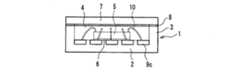
まず、この製造方法により作製される固体撮像装置の構造を、図1〜4に示す。図1は、固体撮像装置の断面図、図2は下面図、図3は側面図である。図4は、一部の要素を取り去って示した固体撮像装置の平面図である。 First, the structure of a solid-state imaging device manufactured by this manufacturing method is shown in FIGS. 1 is a cross-sectional view of a solid-state imaging device, FIG. 2 is a bottom view, and FIG. 3 is a side view. FIG. 4 is a plan view of the solid-state imaging device shown with some elements removed.
1はエポキシ樹脂等の熱硬化性または可塑性樹脂からなる筐体であり、平板状の基板部2上に矩形枠状のリブ3を配置した構造を、一体成形により作製したものである。筐体1の内部空間4に面した基板部2上に、撮像素子5が接合部材6により固定されている。リブ3の上端面には、例えばガラスからなる透光板7が接着剤8により接合され、それにより筐体1の内部空間4が封止されて、パッケージが形成されている。リブ3の高さは、例えば0.1〜1.0mmの範囲、リブ3の幅は、例えば0.1〜1.0mmに設定される。 Reference numeral 1 denotes a housing made of a thermosetting or plastic resin such as an epoxy resin, and is a structure in which a rectangular frame-
筐体1には、複数の金属リード片9が成形時に埋め込まれている。金属リード片9は、筐体1の内部空間4から外部に電気的な導出を行うための部材であり、基板部2の内部空間4側の面に露出した内部端子部9aと、基板部2の裏面の内部端子部9aと対応する位置に露出した外部端子部9bと、筐体1の外側面に露出した側面電極部9cとを有する。撮像素子5の電極(図示せず)と各金属リード片9の内部端子部9aとは、各々金属細線10により接続されている。パッケージ全体の厚みは、例えば2.0mm以下に設定される。図1の固体撮像装置から透光板7を取り去った状態の平面形状を、図4に示す。 A plurality of
図1に示されるように、金属リード片9において、内部端子部9aの位置に対応する裏面が外部端子部9bとなる。また、それらの部分において金属リード片9は基板部2と実質的に同一の厚さを有する。従って、樹脂成形時に、内部端子部9aと外部端子部9bを、上下の金型により挟持してクランプすることが可能である。それにより、内部端子部9aの面が上金型の面に押圧されて密着し、樹脂ばりの発生が抑制される。金属リード片9におけるリブ3の下部に位置する部分は、ハーフエッチにより肉薄になっており、下面が樹脂に覆われている。 As shown in FIG. 1, in the
図1および3に示されるように、筐体1の各外側面すなわちリブ3の外周面は、基板部2の面に対して実質的に直交する平面を形成している。また、透光板7の端面および側面電極部9cの表面は、筐体1の外側面と実質的に同一平面を形成している。筐体1の各外側面すなわちリブ3の内周面は、樹脂成形後の金型の抜けを容易にするため、基板部2の面から透光板7に向かって開く向きのテーパが形成されている(図示省略)。 As shown in FIGS. 1 and 3, each outer surface of the housing 1, that is, the outer peripheral surface of the
本実施の形態における固体撮像装置の製造方法は、以上のような構造を有する固体撮像装置を、効率的かつ高精度で作製可能であり、図5〜7を参照して以下に説明する工程により実施される。 The manufacturing method of the solid-state imaging device according to the present embodiment can manufacture the solid-state imaging device having the above-described structure efficiently and with high accuracy, and includes the steps described below with reference to FIGS. To be implemented.
先ず図5(a)に示すように、リードフレーム21を用意する。リードフレーム21は、図6の平面形状に示されるように、図1に示した金属リード片9を形成するためのリード部22を複数本連結したものである。各リード部22の内部端子部9aに対応する位置における厚みは、基板部2の厚みと実質的に同一に設定される。リード部22はその下面にハーフエッチにより形成された凹部23を有し、後の工程においてこの部分で切断されることにより、図1に示した金属リード片9の形状になる。 First, as shown in FIG. 5A, a
次に、図5(b)に示すように、リードフレーム21を埋め込んで、樹脂の一体成形により、基板部24およびリブ形成部材25からなる筐体26を複数個含む成型体を作製する。成形後の平面形状を、図7に示す。リード部22の上下面は、各々基板部24の上下面から露出するように埋め込まれて、各々内部端子部9aおよび外部端子部9bを形成する。リブ形成部材25は、隣接する筐体26のリブを一本に合体させたものである。リブ形成部材25の上端面の中央部には凸部25aを、リブ形成部材25の長手方向に延在するように形成する(図7参照)。したがって、凸部25aの両側に段差部が形成され、各筐体26の内部では、リブ形成部材25の上端面に低段部25bが形成される。 Next, as shown in FIG. 5B, the
次に、図5(c)に示すように、リブ形成部材25により包囲された各筐体26の内部空間内に、撮像素子5を接着材6により固定して、撮像素子5のパッド電極(図示せず)と各内部端子部9aとを金属細線10により接続する。次に、凸部25aの両側の低段部25bの上端面に、接着材28を塗布する。 Next, as shown in FIG. 5C, the
次に図5(d)に示すように、透光板7を載置して接合する。透光板7は、各筐体26に対応させた形状・寸法を有する。具体的には、透光板7の周縁が、凸部25aの側壁より内側、すなわち低段部25bの上端面に面する大きさとする。従って、透光板7を載置する際には、凸部25aの側壁により位置規制されるので、リブ形成部材25の上端面での透光板7の位置決めを容易に行うことができる。 Next, as shown in FIG.5 (d), the
透光板7が接着材28により接合された後、リブ形成部材25、リード部22および基板部24を、ダイシングブレード29により切断して、図5(e)に示すように、各固体撮像装置を形成する個片に分離する。切断は、図5(d)に示したとおり、基板部24に直交する方向であって、かつ平面形状において各リブ形成部材25の幅を2分する方向に行う。その際、リブ形成部材25における凸部25aの領域が削除されるようにする。その結果、分断されたリブ形成部材25、リード部22および基板部24により、基板部2およびリブ3からなる筐体1と、金属リード片9が形成される。また、金属リード片9の側面電極部9cが露出する。 After the
本実施の形態における製造方法によれば、リブ形成部材25の上端面に透光板7を載置する際に、凸部25aが形成する段差部の内周縁により透光板27が位置規制することができる。そのため、リブ形成部材25の上端面の幅を小さくしても透光板27の位置決めが容易かつ確実であり、リブ形成部材25の幅の大きさが筐体の小型化の障害となることはない。しかも、最終的に段差部の凸部25aを削除するので、位置規制のための凸部25aの形成が筐体の小型化に対する障害となることもない。 According to the manufacturing method in the present embodiment, when the
なお、隣接する筐体26の2本のリブが一体に形成された1本のリブ形成部材25は、1本のリブを個別に成形する場合の幅の2倍より小さい幅に設定可能である。したがって、これを図5(e)に示すように半分に切断すれば、各固体撮像装置におけるリブ3の幅は、1本のリブを個別に成形した場合に比べると小さくなり、その分、固体撮像装置の面積が縮小される。 In addition, the single
このようにしても、リブ形成部材25の幅は、透光板7を接合するための接着材の塗布には十分な範囲に確保可能である。極端な例では、個別に成形する場合の1本分の幅でリブ形成部材25を成形し、それを2分割すれば、切断後のリブ3を幅を従来例の半分にすることができる。 Even in this case, the width of the
また、リブ形成部材25を幅方向に2分して切断することにより、切断面は基板部24に垂直になる。これに対して、従来のようにリブを個別に成形する場合、リブの外側面には、成形後に金型から抜くためのテーパが形成される。従って、本実施の形態により作製されるリブは、テーパ部が存在しない分だけ、リブの幅が低減される。 Further, by cutting the
さらに、リブ形成部材25およびリード部22が同一のダイシングブレード29により一括して切断されるので、透光板7の端面、筐体1の側面および金属リード片9の端面が形成するパッケージ側面は、実質的に同一平面となり、良好な平坦度を得ることができる。したがって、光学系を収容した鏡筒を装着する際、パッケージの側面を利用して、撮像素子5の受光部に対する光学系の位置決めを高精度で行うことができる。すなわち、パッケージの側面と鏡筒の内面の当接により水平位置を容易に位置決めすることができる。なお、垂直方向の位置決めは、回路基板面と鏡筒の下面との当接により行うことができる。 Further, since the
次に、上述の製造工程の図5(b)に示した、樹脂による筐体の成形工程について、図8を参照して具体的に説明する。 Next, the molding process of the casing made of resin shown in FIG. 5B of the manufacturing process described above will be specifically described with reference to FIG.
まず図8(a)に示すように、上金型30および下金型31の間にリードフレームを配置して、リード部22の上下面を、上金型30および下金型31でクランプする。下金型31の上面は平面であるが、上金型30の下面には、リブ形成部材25(図5参照)を形成するための凹部32が設けられている。凹部32の中央部には、リブ形成部材25の凸部25aを形成するための溝部30aが設けられている。リード部22を介することにより上金型30および下金型31の間に形成された空間部33、上金型30の凹部32の空間部、およびリード部22の凹部23の空間部が、樹脂成形用のキャビティを形成する。 First, as shown in FIG. 8A, a lead frame is disposed between the
次に図8(b)に示すように、キャビティに樹脂を充填して、基板部24およびリブ形成部材25を成形する。その後図8(c)に示すように、金型を開いて、図5(b)に示したような、筐体が連結された成型体を取り出す。 Next, as shown in FIG. 8B, the
この成形工程においては、リード部22の上下面を、上金型30および下金型31でクランプすることにより、金型面とリード部22の上下面が密着した状態を安定して得ることができる。また、上金型30の凹部32の境界部は、リード部22の上面に配置される。以上の結果、成形による樹脂ばりの発生が効果的に抑制される。 In this molding step, the upper and lower surfaces of the
また、筐体の樹脂成形に際して、金型とリードフレーム21の間に、樹脂フラッシュバリの発生を抑制するための樹脂シートを介在させれば、ばりの発生をより効果的に抑制できる。 Further, when the resin molding of the housing is performed, if a resin sheet for suppressing the generation of resin flash burrs is interposed between the mold and the
以上の説明では、隣接する筐体を形成するリブを一本に合体させて形成する例を示したが、従来例において示したように、隣接する各リブを分離して形成する方法を採用する場合であっても、本実施の形態の製造方法を適用して同様の効果を得ることが可能である。 In the above description, an example in which the ribs forming the adjacent housings are combined into one is shown. However, as shown in the conventional example, a method of separately forming the adjacent ribs is adopted. Even in this case, the same effect can be obtained by applying the manufacturing method of the present embodiment.
本発明の固体撮像装置の製造方法によれば、リブの上端面に対する透光板の位置決めが容易であって、しかも完成後にリブ幅が小さく、筐体を小型化することが可能であり、ビデオカメラやスチルカメラ等に用いられる固体撮像装置の製造に有用である。 According to the method for manufacturing a solid-state imaging device of the present invention, it is easy to position the translucent plate with respect to the upper end surface of the rib, the rib width is small after completion, and the housing can be downsized. This is useful for manufacturing a solid-state imaging device used for a camera, a still camera, or the like.
1 筐体
2 基板部
3 リブ
4 内部空間
5 撮像素子
6 接合部材
7 透光版
8 接着材
9 金属リード片
9a 内部端子部
9b 外部端子部
9c 側面電極部
10 金属細線
21 リードフレーム
22 リード部
23 凹部
24 基板部
25 リブ形成部材
25a 凸部
25b 低段部
26 筐体
28 接着材
29 ダイシングブレード
30 上金型
30a 溝部
31 下金型
32 凹部
33 空間部
DESCRIPTION OF SYMBOLS 1 Housing | casing 2 Board |
Claims (2)
Translated fromJapanese前記筐体の内部空間内の前記基板部上に撮像素子を固定する工程と、
前記撮像素子の電極と前記各金属リード片の前記内部端子部とを各々接続する工程と、
前記低段部上面に接着材を充填する工程と、
前記リブの前記段差部に形成された内壁の内側領域内で前記低段部の上面に載置可能な大きさの透光板を前記段差部の内壁により位置規制しながら前記低段部上面の前記接着材上に載置し接合する工程と、
前記リブの前記段差部の外側に位置する部分を削除する工程と
を備えたことを特徴とする固体撮像装置の製造方法。A housing formed of a substrate portion and a rectangular frame-shaped rib is integrally molded with a plurality of metal lead pieces, and an internal terminal portion and an external terminal portion are formed by each of the metal lead pieces, and therib Forming a stepped portion by providing a lower stepped portion along the inner periphery on the upper end surface of
And fixing the image pickup element on the substrate portion of theinternal spaceof thehousing,
A step of respectivelyconnectingthe internal terminal portions of the electrodes and the respective metal lead pieces of the imagesensor,
Filling the lower step portion with an adhesive; and
A translucent plate of a size that can be placed on the upper surface of the lower step portion in the inner region of the inner wall formed in the step portion of the rib is positioned on the upper surface of the lower step portion while regulating the position by the inner wall of the step portion. Placing and bonding on the adhesive;and
Removingthe portion of the rib located outside the stepped portion;
A method for manufacturing a solid-state imaging device.
前記各筐体の内部空間内の前記基板部上にそれぞれ撮像素子を固定する工程と、
前記撮像素子の電極と前記各金属リード片の前記内部端子部とを各々接続する工程と、
前記リブ形成部材の前記凸部の両側に形成された低段部の上面に接着材を充填する工程と、
前記リブ形成部材の前記凸部に形成された内壁の内側領域内で前記低段部の上面に載置可能な大きさの透光板を前記凸部の内壁により位置規制しながら、前記低段部上面の前記接着材上に載置し接合する工程と、
前記各筐体毎に、前記基板部に直交し且つ前記各リブ形成部材の幅を2分する方向に、前記凸部を削除するように切断して、固体撮像装置を各個片に分離する工程と
を備えたことを特徴とする固体撮像装置の製造方法。
A plurality of housings formed by the substrate portion and the rectangular frame-shaped ribs are collectivelymolded together with a plurality of metal lead pieces arranged in each of the housings, and the respective metal leads An internal terminal portion and an external terminal portion are formed by apiece, and the ribs forming the adjacent housings are combined into one to form a rib forming member, and the width of the upper end surface of the rib forming member isa step of Ru formed a convex portion extending in placed lengthwise in the centerdirection,
Fixingan image sensor oneach of the substrate portions in the internal space of each housing;
A step of respectivelyconnectingthe internal terminal portions of the electrodes and the respective metal lead pieces of the imagesensor,
Filling the upper surface of the low step portion formed on both sides of the convex portion of the rib forming member with an adhesive;
The translucent plate having a size that can be placed on the upper surface of the low step portion in the inner region of the inner wall formed on the convex portion of the rib forming member is regulated by theinner wall of the convex portion, and the low step Placing and bonding on the adhesive on the top surface of the part;
Wherein each casing, the width of the orthogonal and each rib forming members on the substrate portion in the direction of 2 minutes, and cut to remove the protrudingportion, for separating thesolid-state imaging device to respective piecesProcess and
A method for manufacturinga solid-state imaging device.
Priority Applications (6)
| Application Number | Priority Date | Filing Date | Title |
|---|---|---|---|
| JP2003293545AJP3838571B2 (en) | 2003-08-14 | 2003-08-14 | Method for manufacturing solid-state imaging device |
| TW093122375ATW200507222A (en) | 2003-08-14 | 2004-07-27 | Method for manufacturing solid-state imaging devices |
| US10/901,850US7268016B2 (en) | 2003-08-14 | 2004-07-28 | Method for manufacturing solid-state imaging devices |
| EP04018210AEP1507295A3 (en) | 2003-08-14 | 2004-07-31 | Method for manufacturing solid-state imaging devices |
| CNA2004100562289ACN1581502A (en) | 2003-08-14 | 2004-08-05 | Method for manufacturing solid-state imaging devices |
| KR1020040063816AKR100644185B1 (en) | 2003-08-14 | 2004-08-13 | Method for manufacturing solid-state imaging devices |
Applications Claiming Priority (1)
| Application Number | Priority Date | Filing Date | Title |
|---|---|---|---|
| JP2003293545AJP3838571B2 (en) | 2003-08-14 | 2003-08-14 | Method for manufacturing solid-state imaging device |
Publications (2)
| Publication Number | Publication Date |
|---|---|
| JP2005064292A JP2005064292A (en) | 2005-03-10 |
| JP3838571B2true JP3838571B2 (en) | 2006-10-25 |
Family
ID=33562806
Family Applications (1)
| Application Number | Title | Priority Date | Filing Date |
|---|---|---|---|
| JP2003293545AExpired - Fee RelatedJP3838571B2 (en) | 2003-08-14 | 2003-08-14 | Method for manufacturing solid-state imaging device |
Country Status (6)
| Country | Link |
|---|---|
| US (1) | US7268016B2 (en) |
| EP (1) | EP1507295A3 (en) |
| JP (1) | JP3838571B2 (en) |
| KR (1) | KR100644185B1 (en) |
| CN (1) | CN1581502A (en) |
| TW (1) | TW200507222A (en) |
Families Citing this family (16)
| Publication number | Priority date | Publication date | Assignee | Title |
|---|---|---|---|---|
| US20070040231A1 (en)* | 2005-08-16 | 2007-02-22 | Harney Kieran P | Partially etched leadframe packages having different top and bottom topologies |
| KR20060004885A (en)* | 2005-12-24 | 2006-01-16 | 최현규 | Semiconductor package, manufacturing method and semiconductor package module for image sensor |
| CN100454505C (en)* | 2006-01-25 | 2009-01-21 | 矽品精密工业股份有限公司 | Semiconductor device and method for fabricating the same |
| US7990727B1 (en)* | 2006-04-03 | 2011-08-02 | Aprolase Development Co., Llc | Ball grid array stack |
| US8609978B2 (en)* | 2007-02-14 | 2013-12-17 | Flextronics Ap, Llc | Leadframe based photo voltaic electronic assembly |
| JP2008227233A (en)* | 2007-03-14 | 2008-09-25 | Matsushita Electric Ind Co Ltd | Semiconductor device manufacturing method, optical pickup module, and semiconductor device |
| JP5132957B2 (en)* | 2007-03-14 | 2013-01-30 | パナソニック株式会社 | Semiconductor device, manufacturing method thereof, and optical pickup module |
| JP2008226378A (en)* | 2007-03-14 | 2008-09-25 | Matsushita Electric Ind Co Ltd | Semiconductor device, manufacturing method thereof, and optical pickup module |
| JP2008227232A (en)* | 2007-03-14 | 2008-09-25 | Matsushita Electric Ind Co Ltd | Semiconductor device manufacturing method, semiconductor device, and optical pickup module |
| DE102007024159B3 (en)* | 2007-05-24 | 2008-11-06 | Semikron Elektronik Gmbh & Co. Kg | The power semiconductor module |
| KR100927423B1 (en)* | 2008-05-15 | 2009-11-19 | 삼성전기주식회사 | Glass cap molding package and manufacturing method thereof, and camera module |
| JP5633480B2 (en)* | 2011-06-30 | 2014-12-03 | 豊田合成株式会社 | Method for manufacturing light emitting device |
| JP2015038920A (en)* | 2013-08-19 | 2015-02-26 | ソニー株式会社 | Imaging apparatus and electronic apparatus |
| KR102403839B1 (en)* | 2016-03-08 | 2022-05-31 | 주식회사 쿠라레 | Manufacturing method of metal-clad laminate and metal-clad laminate |
| WO2019156051A1 (en)* | 2018-02-08 | 2019-08-15 | 株式会社村田製作所 | High-frequency module |
| JP7181050B2 (en)* | 2018-10-18 | 2022-11-30 | 浜松ホトニクス株式会社 | Radiation imaging device |
Family Cites Families (6)
| Publication number | Priority date | Publication date | Assignee | Title |
|---|---|---|---|---|
| JP2001077277A (en) | 1999-09-03 | 2001-03-23 | Sony Corp | Semiconductor package and its manufacture |
| US6384472B1 (en)* | 2000-03-24 | 2002-05-07 | Siliconware Precision Industries Co., Ltd | Leadless image sensor package structure and method for making the same |
| JP2002134762A (en)* | 2000-10-19 | 2002-05-10 | Shinko Electric Ind Co Ltd | Optical device and method of manufacturing the same |
| TW473951B (en)* | 2001-01-17 | 2002-01-21 | Siliconware Precision Industries Co Ltd | Non-leaded quad flat image sensor package |
| JP2002373950A (en) | 2001-06-15 | 2002-12-26 | Seiko Instruments Inc | Method for manufacturing hermetically sealed ic package |
| TW521410B (en)* | 2001-11-15 | 2003-02-21 | Siliconware Precision Industries Co Ltd | Semiconductor package article |
- 2003
- 2003-08-14JPJP2003293545Apatent/JP3838571B2/ennot_activeExpired - Fee Related
- 2004
- 2004-07-27TWTW093122375Apatent/TW200507222A/enunknown
- 2004-07-28USUS10/901,850patent/US7268016B2/ennot_activeExpired - Fee Related
- 2004-07-31EPEP04018210Apatent/EP1507295A3/ennot_activeWithdrawn
- 2004-08-05CNCNA2004100562289Apatent/CN1581502A/enactivePending
- 2004-08-13KRKR1020040063816Apatent/KR100644185B1/ennot_activeExpired - Fee Related
Also Published As
| Publication number | Publication date |
|---|---|
| EP1507295A3 (en) | 2006-05-24 |
| US20050037538A1 (en) | 2005-02-17 |
| EP1507295A2 (en) | 2005-02-16 |
| US7268016B2 (en) | 2007-09-11 |
| CN1581502A (en) | 2005-02-16 |
| KR100644185B1 (en) | 2006-11-10 |
| KR20050019056A (en) | 2005-02-28 |
| TW200507222A (en) | 2005-02-16 |
| JP2005064292A (en) | 2005-03-10 |
Similar Documents
| Publication | Publication Date | Title |
|---|---|---|
| JP3782405B2 (en) | Solid-state imaging device and manufacturing method thereof | |
| JP3782406B2 (en) | Solid-state imaging device and manufacturing method thereof | |
| JP3838572B2 (en) | Solid-state imaging device and manufacturing method thereof | |
| US7719585B2 (en) | Solid-state imaging device | |
| JP3838571B2 (en) | Method for manufacturing solid-state imaging device | |
| JP4106003B2 (en) | Method for manufacturing solid-state imaging device | |
| JP4219943B2 (en) | Solid-state imaging device | |
| JP2006332686A (en) | Solid-state imaging device | |
| JP4147171B2 (en) | Solid-state imaging device and manufacturing method thereof |
Legal Events
| Date | Code | Title | Description |
|---|---|---|---|
| A621 | Written request for application examination | Free format text:JAPANESE INTERMEDIATE CODE: A621 Effective date:20041224 | |
| A977 | Report on retrieval | Free format text:JAPANESE INTERMEDIATE CODE: A971007 Effective date:20060428 | |
| A131 | Notification of reasons for refusal | Free format text:JAPANESE INTERMEDIATE CODE: A131 Effective date:20060615 | |
| A521 | Request for written amendment filed | Free format text:JAPANESE INTERMEDIATE CODE: A523 Effective date:20060705 | |
| TRDD | Decision of grant or rejection written | ||
| A01 | Written decision to grant a patent or to grant a registration (utility model) | Free format text:JAPANESE INTERMEDIATE CODE: A01 Effective date:20060727 | |
| A61 | First payment of annual fees (during grant procedure) | Free format text:JAPANESE INTERMEDIATE CODE: A61 Effective date:20060728 | |
| R150 | Certificate of patent or registration of utility model | Free format text:JAPANESE INTERMEDIATE CODE: R150 | |
| FPAY | Renewal fee payment (event date is renewal date of database) | Free format text:PAYMENT UNTIL: 20090811 Year of fee payment:3 | |
| FPAY | Renewal fee payment (event date is renewal date of database) | Free format text:PAYMENT UNTIL: 20100811 Year of fee payment:4 | |
| FPAY | Renewal fee payment (event date is renewal date of database) | Free format text:PAYMENT UNTIL: 20110811 Year of fee payment:5 | |
| LAPS | Cancellation because of no payment of annual fees |