JP3836166B2 - Two-layer transistor and manufacturing method thereof - Google Patents
Two-layer transistor and manufacturing method thereofDownload PDFInfo
- Publication number
- JP3836166B2 JP3836166B2JP31122894AJP31122894AJP3836166B2JP 3836166 B2JP3836166 B2JP 3836166B2JP 31122894 AJP31122894 AJP 31122894AJP 31122894 AJP31122894 AJP 31122894AJP 3836166 B2JP3836166 B2JP 3836166B2
- Authority
- JP
- Japan
- Prior art keywords
- wiring
- drain
- source
- film
- tft
- Prior art date
- Legal status (The legal status is an assumption and is not a legal conclusion. Google has not performed a legal analysis and makes no representation as to the accuracy of the status listed.)
- Expired - Fee Related
Links
Images


Landscapes
- Metal-Oxide And Bipolar Metal-Oxide Semiconductor Integrated Circuits (AREA)
- Thin Film Transistor (AREA)
Description
Translated fromJapanese【0001】
【産業上の利用分野】
本発明は、ガラス等の絶縁材料、あるいはシリコンウェハー上に設けられた酸化珪素等の絶縁表面上に形成される絶縁ゲイト型電界効果トランジスタ(TFT)を用いた半導体集積回路に関する。本発明は、多層構造のトランジスタを用いた集積回路(多層型半導体集積回路、立体型半導体集積回路、3次元型半導体集積回路ともいう)に関するもので、例えば、第1層のトランジスタとして、単結晶半導体表面に設けられた電界効果トランジスタ、第2層のトランジスタとしてTFTを用いたものや、第1層および第2層のトランジスタとしてTFTを用いたものに関するものである。
【0002】
【従来の技術】
近年、半導体集積回路の集積度を向上させるため、集積回路を多層構造とした多層型集積回路が提案されている。このような多層型集積回路としては、シリコンウェファーのような単結晶基板上に第1層の半導体素子層を形成し、その上にTFTを用いて第2層の半導体素子層を形成するというものである。こうすることにより、トランジスタの面積を従来より半減することが可能となった。このような多層型集積回路は、上記の例に限らず、第1層、第2層ともTFTであってもよいし、さらに第3層、第4層の半導体素子層が設けられてもよい。
【0003】
【発明が解決しようとする課題】
しかし、これまでは第1層のトランジスタと第2層のトランジスタの接続についてはあまり考慮されることがなかった。例えば、下層のトランジスタのソース(もしくはドレイン)と上層のトランジスタのゲイト配線を接続する場合には、上層のゲイト配線を形成した後で、その上に層間絶縁物を形成して、それをエッチングして、下層のトランジスタのソースおよび上層のトランジスタのゲイト配線にコンタクトホールを形成し、このコンタクトを結ぶ配線を前記層間絶縁物上に形成していた。
【0004】
すなわち、下層のトランジスタの層間絶縁物形成後の工程は以下のようになった。
▲1▼上層のトランジスタ(TFT)の活性半導体層およびゲイト絶縁膜の形成
▲2▼TFTのゲイト配線の形成
▲3▼TFTのソース/ドレインの形成
▲4▼TFTの第1の層間絶縁物の形成
▲5▼下層のトランジスタのソースへのコンタクトホールの形成。
▲6▼TFTのゲイト配線へのコンタクトホールの形成。
▲7▼第1の層間配線の形成(下層のトランジスタのソースとTFTのゲイト配線を結ぶ)
▲8▼TFTの第2の層間絶縁物の形成
▲9▼TFTのソースもしくはドレインへのコンタクトホールの形成と第2の層間配線の形成(TFTのソースもしくはドレインから延びる配線)
【0005】
上記の例では、工程▲5▼および▲6▼において、下層のトランジスタのソースとTFTのゲイト配線とのコンタクトは同時に形成できなくはないが、現実には、下層トランジスタのソースのコンタクトホールは、下層トランジスタを覆う層間絶縁物とTFTの第1の層間絶縁物をエッチングしなければならないのに対し、TFTのゲイト配線のコンタクトホールはTFTの第1の層間絶縁物をエッチングするだけでよく、ホールの深さにして、0.3〜1μm程度の差が生じ、例えば、TFTのゲイト配線のオーバーエッチ等をもたらし、エッチング工程における歩留りを低下させる原因となった。このため、通常は、上記のように2工程に分けておこなわれた。
本発明はこのような問題点に鑑みてなされたものであり、プロセスをより簡単にすることを目的とする。
【0006】
【課題を解決するための手段】
本発明においては、下層のトランジスタのソースもしくはドレインのどちらか一方を上層のトランジスタ(TFT)のゲイト配線とコンタクトさせることによって、上記の問題を解決する。この場合、TFTのゲイト配線の終端の一方は、下層のトランジスタのソースもしくはドレインのいずれか一方である。特に、本発明においては、TFTの配線をアルミニウムを主成分とする材料によって構成し、さらに、TFTのソース/ドレインへ不純物を導入する工程もしくは導入後の工程にレーザーを用いることを特徴とする。例えば、不純物をイオン注入等の手段によってTFTの活性半導体層に導入した後、レーザーアニールをおこなう方法や、不純物を含む雰囲気(ジボランやホスフィン)中においてレーザー照射をおこなう方法(レーザードーピング)である。
【0007】
【作用】
本発明を用いて、先に示した下層のトランジスタのソースとTFTのゲイト配線の接続する場合のプロセスは以下のようになる。
▲1▼上層のトランジスタ(TFT)の活性半導体層およびゲイト絶縁膜の形成
▲2▼下層のトランジスタのソースへのコンタクトホールの形成。
▲3▼TFTのゲイト配線の(=下層トランジスタのソースへの配線)形成
▲4▼TFTのソース/ドレインの形成
▲6▼TFTの層間絶縁物の形成
▲7▼TFTのソースもしくはドレインへのコンタクトホールの形成。
▲8▼第2の層間配線の形成(TFTのソースもしくはドレインから延びる配線)
このように、コンタクトホールおよび層間絶縁物の形成の工程が省略され、歩留りが向上する。
【0008】
【実施例】
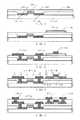
〔実施例1〕 図1に本発明の例(作製工程断面図)を示す。まず、単結晶シリコンウェハー101上面に公知のMOSプロセスによって下層のトランジスタを形成した。すなわち、フィールド絶縁物102、ゲイト熱酸化膜103、N+型多結晶シリコンのゲイト電極104、N型のソース105、ドレイン106、層間絶縁物107を形成した。ソース/ドレインは、低濃度ドレイン(LDD)を有する構成としてもよい。層間絶縁物はCVD法等によって、できるだけ平坦になるように形成し、場合によっては、化学的機械研磨(CMP)法によって、表面を平坦化してもよい。このような処理をした後、窒素雰囲気中、900〜1100℃で、1〜5時間アニールして、層間絶縁物107の表面を緻密化した。(図1(A))
【0009】
その後、プラズマCVD法やLPCVD法によってアモルファスシリコン膜を100〜5000Å、好ましくは300〜1000Å堆積し、これを、550〜600℃の還元雰囲気に4〜24時間放置して、結晶化せしめた。この工程は、レーザー照射によっておこなってもよい。そして、このようにして結晶化させたシリコン膜をパターニング・エッチングして、TFTの活性半導体層108とした。さらに、酸素雰囲気中、900〜1100℃で、1〜5時間アニールして、表面に熱酸化膜109を形成した。(図1(B))
【0010】
その後、層間絶縁物107をエッチングして、下層のトランジスタのソース105、ドレイン106にコンタクトホールを形成した。そして、厚さ1000Å〜3μmのアルミニウム(1wt%のSi、もしくは0.1〜0.3wt%のSc(スカンジウム)を含む)膜を電子ビーム蒸着法もしくはスパッタ法によって形成した。この際には、以下のような多段階の成膜プロセス(例えば、Extended Abstracts of 1993 International Conference on Solid State Devices andMaterials, Makuhari, 1993, pp180-182) を経てもよかった。すなわち、最初にジメチル・アルミニウム・ハイドライド(DMAH、AlH(CH3)2)を用いたCVD法によって、コンタクトホール部に選択的にアルミニウムを形成した。そして、コンタクトホールが完全に埋まった段階で、スパッタ法によって、全面にアルミニウムを形成した。このプロセスはマルチチャンバーシステムにおいて、連続的におこなうことができる。
【0011】
このようにして、アルミニウム膜を形成した後、これをパターニング・エッチングして、下層のトランジスタのソース配線110、ドレイン配線111、ゲイト配線112を形成した。ここで、注意しなければならないことは、図1では図示されていないが、下層のトランジスタのドレイン配線111とTFTのゲイト配線112は一体となっていることである。したがって、この段階で、下層のトランジスタのドレインとTFTのゲイト配線は電気的に接続されている。(図1(C))
【0012】
そして、イオンドーピング法によって、TFTの活性半導体層108に、ゲイト配線112をマスクとして自己整合的に不純物を注入し、P型のソース113、ドレイン114を形成した。ドーピングガスとしてはジボラン(B2H6)を用いた。その後、KrFエキシマーレーザー(波長248nm、パルス幅20nsec)を照射して、活性層中に導入された不純物イオンの活性化をおこなった。レーザーとしては、XeClエキシマーレーザー(波長308nm、パルス幅50nsec)を用いてもよかった。
【0013】
なおエキシマーレーザー以外に、他のレーザーを用いてもよいことはいうまでもない。パルスレーザーに関しては、Nd:YAGレーザー(Qスイッチパルス発振が望ましい)のごとき赤外光レーザーやその第2高調波のごとき可視光レーザーが使用できる。また、レーザー光は、基板側から照射してもよい。この場合には下に存在する珪素半導体膜を透過するレーザー光を選択する必要がある。このようにして、ソース113、ドレイン114を活性化させた。(図1(D))
【0014】
最後に、全面に層間絶縁物115として、CVD法によって酸化珪素膜を厚さ2000Å〜1μm、例えば、3000Å形成した。さらに、TFTのソース113、ドレイン114、および下層のトランジスタのソース配線110にコンタクトホールを形成し、アルミニウム配線116、117、118を2000Å〜1μm、例えば5000Åの厚さに形成した。このアルミニウム配線116〜118とコンタクトする部分との間にバリヤメタルとして、例えば窒化チタンを形成するとより一層、信頼性を向上させることができた。(図1(E))
【0015】
かくすることにより、相補型の構成を得ることができた。重要なことは、これまでの相補型FETは、多層型であっても、インバータの思想を中心としていたためPチャネルFETとNチャネルFETのゲイト電極を同時に形成していた。しかし、本発明は、相補型FETにおいて、一方のゲイト電極と他方のソースまたはドレインの配線とを金属材料で形成したものである。
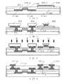
図2、図3には本実施例を用いて、フリップフロップ回路を形成する例を示す。図2(A)は、下層トランジスタのソース/ドレインおよびゲイト配線等を示す。図の左上の十文字200はマーカーを意味する。図の斜線部はソース/ドレインを表し、太線はゲイト配線を意味する。すなわち、図2(A)においては、下層トランジスタのドレイン201、202、同じくソース203、ゲイト配線206、207が示される。ソース203は、そのまま電源供給線204、205となり、接地される。(図2(A))
【0016】
図2(B)は、TFTのソース/ドレイン(活性半導体層)およびゲイト配線、コンタクトの位置等を示す。図の斜線部はソース/ドレインを表し、太線はゲイト配線を意味する。すなわち、図2(B)においては、TFTのドレイン208、209、同じくソース210、ゲイト配線213、212が示される。ソース210は、そのまま電源供給線211、212となり、外部の電源に接続される。コンタクト215は下層のトランジスタのゲイト配線206に、コンタクト216は下層のトランジスタのドレイン202に、コンタクト218は下層のトランジスタのゲイト配線207に、コンタクト217は下層のトランジスタのドレイン201に、それぞれ接続する。また、コンタクト215と216、およびコンタクト217と218が、それぞれTFTのゲイト配線213、214によって接続されるため、下層の第1のトランジスタのゲイト配線206と第2のトランジスタのドレイン202、および、下層の第2のトランジスタのゲイト配線207と第2のトランジスタのドレイン201が互いに接続される。
【0017】
図2(C)は、TFTのソース/ドレイン配線とコンタクトの位置を示す。すなわち、図2(C)においては、第1のTFTのドレイン208と第2のTFTのゲイト配線214がコンタクト221、222と配線219によって接続され、同じく、第2のTFTのドレイン209と第1のTFTのゲイト配線213がコンタクト223、224と配線220によって接続される。(図2(C))
図2から特徴的なことは、下層のトランジスタのチャネルとTFTのチャネルが60〜120°の角度をなすように配置されていることであり、こうすることにより無駄なスペースを極力無くすことができる。より集積度を高めるには、この角度は80〜100°、好ましくは90°となるようにすることが効果的である。
【0018】
図3(B)は、図2(A)および(B)を重ね合わせたものである。重なりがわるように、意図的に重なりをわずかにずらしてある。図3(C)は、図3(B)にさらに、図2(C)を重ねたものである。このようにして、図3(A)に示すようなフリップフロップ回路が得られた。図3(A)の点A、B、C、D、E、F、G、Hは、図2の216(223、224)、215、218、217(221、222)、204、205、211、212に、それぞれ対応する。
【0019】
本実施例をさらに発展させて、CMOSフリップフロップ回路を用いたスタティックRAM(SRAM)を構成した例を図4に示す。図の点線で囲まれた部分は、SRAMの1ビットセルの専有面積を示す。図3(D)は図3(A)のフリップフロップ回路に選択トランジスタを左右に付属させたSRAMの単位回路を示す。同様に本発明の構成を用いることによりセル面積をより小さくすることができる。
図4(A)は、このSRAM回路の下層トランジスタのソース/ドレインおよびゲイト配線等を示す。図の斜線部はソース/ドレインを表し、太線はゲイト配線を意味する。すなわち、図2(A)においては、下層トランジスタのドレイン401、402、選択トランジスタのソース403、404、ゲイト配線405、406、およびワード線(選択トランジスタのゲイト配線)407が示される。下層トランジスタのソースはVLの電位に保たれる。(図4(A))
【0020】
図4(B)は、TFTのソース/ドレイン(活性半導体層)およびゲイト配線、コンタクトの位置等を示す。図の斜線部はソース/ドレインを表し、太線はゲイト配線等を意味する。すなわち、図4(B)においては、TFTのドレイン408、409、ゲイト配線410、411、選択トランジスタのソース配線412、413が示される。TFTのソースは、そのままVHの電位に保たれる。ゲイト配線410、411のコンタクトの配置は、実質的には図2(B)のものと同じである。(図4(B))
【0021】
図4(C)は、TFTのソース/ドレイン配線とコンタクトの位置を示す。すなわち、図4(C)においては、第1のTFTのドレイン408と第2のTFTのゲイト配線411が配線416によって接続され、同じく、第2のTFTのドレイン409と第1のTFTのゲイト配線410が配線417によって接続される。また、ビット線(選択トランジスタのソース配線)414、415もこの層に設けられる。(図4(C))
図4(D)は、図4(A)、(B)、(C)を重ね合わせたものである。このようにして、SRAMの1ビットセルが形成される。図4に示したセルは1ビットの面積を極力少なくするようにレイアウトされたものである。
【0022】
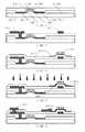
〔実施例2〕 図5に本発明の例(作製工程断面図)を示す。まず、実施例1と同様に単結晶シリコンウェハー501上にフィールド絶縁物502、ゲイト熱酸化膜503、N+型多結晶シリコンのゲイト電極504、P型のソース505、ドレイン506、層間絶縁物507を形成し、下層のトランジスタとした。
その後、アモルファスシリコン膜を100〜5000Å、好ましくは300〜1000Å堆積し、これを、550〜600℃の還元雰囲気に4〜24時間放置して、結晶化せしめた。この工程は、レーザー照射によっておこなってもよい。そして、このようにして結晶化させたシリコン膜をパターニング・エッチングして、TFTの活性半導体層508とした。さらに、酸素雰囲気中、900〜1100℃で、1〜5時間アニールして、表面に熱酸化膜509を形成した。(図5(A))
【0023】
その後、層間絶縁物507をエッチングして、下層のトランジスタのソース505、ドレイン506にコンタクトホールを形成した。そして、厚さ1000Å〜3μmのアルミニウム(1wt%のSi、もしくは0.1〜0.3wt%のSc(スカンジウム)を含む)膜を電子ビーム蒸着法もしくはスパッタ法によって形成した。そして、その表面に公知のスピンコート法によってフォトレジストを形成し、公知のフォトリソグラフィー法によって、パターニングをおこなった。そして、燐酸によって、アルミニウム膜のエッチングをおこなった。このようにして、下層のトランジスタのソース配線510、ドレイン配線511、ゲイト配線512を形成した。この際にも、下層のトランジスタのドレイン配線511とTFTのゲイト配線512は一体となっている。また、これらのアルミニウム配線上にはフォトレジストのマスク513、514、515が残存したままとなり、配線の側面はフォトレジストの側面よりも内側にある。(図5(B))
【0024】
この状態で、イオンドーピング法によって、TFTの活性半導体層508に、フォトレジスト515をマスクとして自己整合的にN型不純物(ここでは燐)を注入し、N型のソース516、ドレイン517を形成した。ここで、フォトレジスト515に対して、ゲイト電極512は距離xだけ内側にあるため、図に示したように、ゲイト電極とソース/ドレインが重ならないオフセット状態となっている。距離xは、アルミニウム配線の際のエッチング時間を加減することによって増減できる。xとしては、0.3〜5μmが好ましかった。このような構造のTFTをオフセットゲイト型TFTという。(図5(C))
【0025】
その後、フォトレジスト513〜515を剥離し、KrFエキシマーレーザー(波長248nm、パルス幅20nsec)を照射して、活性層中に導入された不純物イオンの活性化をおこなった。最後に、全面に層間絶縁物518として、CVD法によって酸化珪素膜を厚さ2000Å〜1μm、例えば、3000Å形成した。さらに、TFTのソース516、ドレイン517、および下層のトランジスタのソース配線510にコンタクトホールを形成し、アルミニウム配線519、520、521を2000Å〜1μm、例えば5000Åの厚さに形成した。(図5(D))
【0026】
本実施例ではTFTはNチャネル型であった。本来であれば、Nチャネル型のTFTでは、移動度が大きい半面、ゲイト電極に負の電圧が印加されるとソース/ドレイン間のリーク電流が増加して実用上の困難をきたすのであるが、本実施例のように、オフセット形とすることによって、ドレイン近傍の電界強度を緩和し、上記のリーク電流を抑制することができた。
実施例1(図1)の場合には、TFTとしてPチャネル型を用いたが、これは移動度が小さく、単結晶シリコン上の移動度の大きなNMOSトランジスタと組み合わせてCMOSを構成する上で問題があったが、本実施例では、下層のMOSトランジスタが移動度の小さいPMOSであり、移動度のバランスが取りやすかった。
【0027】
〔実施例3〕 図6に本発明の例(作製工程断面図)を示す。まず、実施例1と同様に単結晶シリコンウェハー601上にフィールド絶縁物602、ゲイト熱酸化膜603、N+型多結晶シリコンのゲイト電極604を形成した。そして、低濃度の燐イオンを注入して、低濃度N型不純物領域(低濃度N型ドレイン、N型LDD)605、606を形成した。
さらに、全面に絶縁被膜を形成し、これを異方性エッチングすることにより、ゲイト電極の側面に側壁604を形成した。そして、側壁をマスクとして、高濃度の砒素イオンを注入して、N型のソース608、ドレイン607を形成した。ここで、ソース608は図4の回路と同様にVLに保たれる。さらに、層間絶縁物609を形成し、下層のトランジスタとした。(図6(A))
【0028】
その後、層間絶縁物609をエッチングして、下層のトランジスタのドレイン607にコンタクトホールを形成した。そして、厚さ3000Åのアルミニウム(1wt%のSiを含む)膜によって、下層のトランジスタのドレイン配線610と上層のTFTのゲイト配線611を形成した。(図6(B))
さらに、厚さ1200Åの酸化珪素膜612を形成した。この酸化珪素膜はTFTのゲイト絶縁膜として機能する。そして、レーザー照射によって結晶化せしめた。そして、このようにして結晶化させたシリコン膜をパターニング・エッチングして、TFTの活性半導体層613とした。さらに、半導体層上に酸化珪素によって、ドーピングマスク614を形成した。(図6(C))
【0029】
この状態で、イオンドーピング法によって、TFTの活性半導体層613に、硼素イオンを注入し、P型のソース615、ドレイン616を形成した。ここで、ソース615は図4の回路と同様にVHに保たれる。(図6(D))
その後、450℃で1時間の熱アニールをおこない、TFTのソース/ドレインを活性化させた。さらに、下層のトランジスタのドレイン配線617にコンタクトホールを形成し、アルミニウム配線617、6185000Åの厚さに形成した。このようにして、図4に示すものと同等な回路を形成することができた。(図6(E))
【0030】
本実施例ではTFTをボトムゲイト型とすることにより、コンタクトホール開孔の工程を他の実施例よりも減らすことができ、歩留りを向上させるうえで効果的であった。
本発明において、アルミニウムを主成分とする金属材料を上層のトランジスタのゲイト電極として用いる方法を示した。しかし、このアルミニウムをボンディングパッドにまで延在する最上層のアルミニウムに比べて1/4〜1/2の厚さに薄くして、高精度パターンとすることは有効であった。また、この配線を下層のトランジスタのソース/ドレインと同一導電型の半導体またはタングステン等のシリサイドを用いてもよい。
【0031】
【発明の効果】
本発明によって、多層半導体集積回路を歩留り良く作製することができた。本発明に用いられるTFTは、実施例に示したような単純な構造のものだけでなく、低濃度ドレイン(LDD)を有するものや、さまざまなオフセット構造を有するものであってもよいことはいうまでもない。また、下層と上層のトランジスタの導電型は、実施例のように異種のものであっても、また、同じものであってもよい。
【図面の簡単な説明】
【図1】 実施例1によるTFTの作製工程断面図を示す。
【図2】 実施例1によるフリップフロップ回路の配置を示す。
【図3】 実施例1によるフリップフロップ回路の配置を示す。
【図4】 実施例1によるSRAMの回路配置を示す。
【図5】 実施例2によるTFTの作製工程断面図を示す。
【図6】 実施例3によるTFTの作製工程断面図を示す。
【符号の説明】
101 単結晶シリコンウェハー
102 フィールド絶縁物
103 下層のトランジスタのゲイト酸化膜
104 下層のトランジスタのゲイト配線
105 下層のトランジスタのソース
106 下層のトランジスタのドレイン
107 下層のトランジスタの層間絶縁物
108 TFTの活性半導体層
109 TFTのゲイト酸化膜
110 下層のトランジスタのソース配線
111 下層のトランジスタのドレイン配線
112 TFTのゲイト配線
113 TFTのソース
114 TFTのドレイン
115 TFTの層間絶縁物
116〜118 配線[0001]
[Industrial application fields]
The present invention relates to a semiconductor integrated circuit using an insulating gate type field effect transistor (TFT) formed on an insulating surface such as an insulating material such as glass or silicon oxide provided on a silicon wafer. The present invention relates to an integrated circuit using a multilayer transistor (also referred to as a multilayer semiconductor integrated circuit, a three-dimensional semiconductor integrated circuit, or a three-dimensional semiconductor integrated circuit). The present invention relates to a field effect transistor provided on a semiconductor surface, a transistor using a TFT as a second layer transistor, and a transistor using a TFT as a first layer and a second layer transistor.
[0002]
[Prior art]
In recent years, in order to improve the integration degree of a semiconductor integrated circuit, a multilayer integrated circuit having a multilayer structure of the integrated circuit has been proposed. As such a multilayer integrated circuit, a first semiconductor element layer is formed on a single crystal substrate such as a silicon wafer, and a second semiconductor element layer is formed thereon using a TFT. It is. In this way, the area of the transistor can be halved compared to the prior art. Such a multilayer integrated circuit is not limited to the above example, and both the first layer and the second layer may be TFTs, and third and fourth semiconductor element layers may be provided. .
[0003]
[Problems to be solved by the invention]
However, the connection between the first layer transistor and the second layer transistor has not been considered so far. For example, when connecting the source (or drain) of the lower transistor and the gate wiring of the upper transistor, after forming the upper gate wiring, an interlayer insulator is formed on the gate wiring and etched. Thus, a contact hole is formed in the source of the lower transistor and the gate wiring of the upper transistor, and a wiring connecting the contacts is formed on the interlayer insulator.
[0004]
That is, the process after the formation of the interlayer insulator of the lower-layer transistor is as follows.
(1) Formation of active semiconductor layer and gate insulating film of upper transistor (TFT) (2) Formation of gate wiring of TFT (3) Formation of source / drain of TFT (4) Formation of first interlayer insulator of TFT Formation (5) Formation of a contact hole to the source of the underlying transistor.
(6) Formation of a contact hole to the gate wiring of the TFT.
(7) Formation of the first interlayer wiring (connecting the source of the lower transistor and the gate wiring of the TFT)
(8) Formation of TFT second interlayer insulator (9) Formation of contact hole to TFT source or drain and formation of second interlayer wiring (wiring extending from TFT source or drain)
[0005]
In the above example, in steps (5) and (6), the contact between the source of the lower transistor and the gate wiring of the TFT cannot be formed simultaneously, but in reality, the contact hole of the source of the lower transistor is While the interlayer insulator covering the lower transistor and the first interlayer insulator of the TFT must be etched, the contact hole of the gate wiring of the TFT only needs to etch the first interlayer insulator of the TFT. As a result, a difference of about 0.3 to 1 [mu] m is caused, resulting in, for example, over-etching of the gate wiring of the TFT and causing a decrease in yield in the etching process. For this reason, it was usually performed in two steps as described above.
The present invention has been made in view of such problems, and aims to simplify the process.
[0006]
[Means for Solving the Problems]
In the present invention, either the source or drain of the lower transistor is brought into contact with the gate wiring of the upper transistor (TFT) to solve the above problem. In this case, one end of the gate wiring of the TFT is either the source or the drain of the lower transistor. In particular, the present invention is characterized in that the TFT wiring is made of a material mainly composed of aluminum, and a laser is used in a step of introducing impurities into the source / drain of the TFT or a step after the introduction. For example, there are a method of performing laser annealing after introducing impurities into the active semiconductor layer of the TFT by means such as ion implantation, and a method of performing laser irradiation (laser doping) in an atmosphere containing impurities (diborane or phosphine).
[0007]
[Action]
The process for connecting the source of the lower layer transistor and the gate wiring of the TFT described above using the present invention is as follows.
(1) Formation of active semiconductor layer and gate insulating film of upper transistor (TFT) (2) Formation of contact hole to source of lower transistor.
(3) Formation of TFT gate wiring (= wiring to the source of the lower layer transistor) (4) Formation of TFT source / drain (6) Formation of interlayer insulation of TFT (7) Contact to source or drain of TFT Hole formation.
(8) Formation of second interlayer wiring (wiring extending from TFT source or drain)
Thus, the process of forming the contact hole and the interlayer insulator is omitted, and the yield is improved.
[0008]
【Example】
Example 1 FIG. 1 shows an example of the present invention (production process sectional view). First, a lower layer transistor was formed on the upper surface of the single
[0009]
Thereafter, an amorphous silicon film was deposited in an amount of 100 to 5000, preferably 300 to 1000 by plasma CVD or LPCVD, and allowed to stand in a reducing atmosphere at 550 to 600 ° C. for 4 to 24 hours for crystallization. This step may be performed by laser irradiation. Then, the silicon film crystallized in this manner was patterned and etched to form an
[0010]
After that, the
[0011]
After the aluminum film was formed in this way, this was patterned and etched to form the
[0012]
Then, by ion doping, impurities were implanted in a self-aligned manner into the
[0013]
Needless to say, other lasers may be used in addition to the excimer laser. As for the pulse laser, an infrared laser such as an Nd: YAG laser (preferably Q-switch pulse oscillation) or a visible laser such as a second harmonic thereof can be used. Moreover, you may irradiate a laser beam from the board | substrate side. In this case, it is necessary to select a laser beam that passes through the underlying silicon semiconductor film. In this way, the
[0014]
Finally, a silicon oxide film having a thickness of 2000 to 1 μm, for example, 3000 μm, was formed as an
[0015]
In this way, a complementary configuration could be obtained. Importantly, even though the conventional complementary FETs are multi-layered, the gate electrode of the P-channel FET and the N-channel FET has been formed at the same time because the idea of the inverter is the center. However, according to the present invention, in the complementary FET, one gate electrode and the other source or drain wiring are formed of a metal material.
2 and 3 show an example of forming a flip-flop circuit using this embodiment. FIG. 2A shows the source / drain and gate wiring of the lower layer transistor. A
[0016]
FIG. 2B shows the source / drain (active semiconductor layer), gate wiring, contact position, and the like of the TFT. The hatched portion in the figure represents the source / drain, and the thick line represents the gate wiring. That is, in FIG. 2B, the
[0017]
FIG. 2C shows the positions of the source / drain wirings and contacts of the TFT. That is, in FIG. 2C, the
What is characteristic from FIG. 2 is that the channel of the lower-layer transistor and the channel of the TFT are arranged so as to form an angle of 60 to 120 °, so that useless space can be eliminated as much as possible. . In order to further increase the degree of integration, it is effective to make this angle 80 to 100 °, preferably 90 °.
[0018]
FIG. 3B is a superposition of FIGS. 2A and 2B. The overlap is intentionally shifted slightly so that the overlap occurs. FIG. 3C is obtained by further superimposing FIG. 2C on FIG. In this way, a flip-flop circuit as shown in FIG. 3A was obtained. Points A, B, C, D, E, F, G, and H in FIG. 3A are represented by 216 (223, 224), 215, 218, 217 (221, 222), 204, 205, and 211 in FIG. , 212 respectively.
[0019]
FIG. 4 shows an example in which this embodiment is further developed and a static RAM (SRAM) using a CMOS flip-flop circuit is configured. A portion surrounded by a dotted line in the figure indicates an exclusive area of the SRAM 1-bit cell. FIG. 3D shows an SRAM unit circuit in which selection transistors are attached to the left and right of the flip-flop circuit of FIG. Similarly, the cell area can be further reduced by using the configuration of the present invention.
FIG. 4A shows the source / drain and gate wiring of the lower layer transistor of this SRAM circuit. The hatched portion in the figure represents the source / drain, and the thick line represents the gate wiring. That is, FIG. 2A shows drains 401 and 402 of lower layer transistors, sources 403 and 404 of selection transistors, gate wirings 405 and 406, and word lines (gate wirings of selection transistors) 407. The source of the lower transistor is kept at a potential ofVL . (Fig. 4 (A))
[0020]
FIG. 4B shows the source / drain (active semiconductor layer), gate wiring, contact position, and the like of the TFT. The hatched portion in the figure represents the source / drain, and the thick line represents a gate wiring or the like. That is, FIG. 4B shows TFT drains 408 and 409, gate wirings 410 and 411, and selection transistor source wirings 412 and 413. The source of the TFT is kept at the potential of VH as it is. The arrangement of the contacts of the
[0021]
FIG. 4C shows the positions of the source / drain wirings and contacts of the TFT. That is, in FIG. 4C, the drain 408 of the first TFT and the
FIG. 4D is a superposition of FIGS. 4A, 4B, and 4C. In this way, a 1-bit cell of SRAM is formed. The cell shown in FIG. 4 is laid out so as to minimize the area of 1 bit.
[0022]
Example 2 FIG. 5 shows an example of the present invention (production process sectional view). First, as in the first embodiment, a field insulator 502, a gate
Thereafter, an amorphous silicon film was deposited to a thickness of 100 to 5000, preferably 300 to 1000, and left to stand in a reducing atmosphere at 550 to 600 ° C. for 4 to 24 hours for crystallization. This step may be performed by laser irradiation. Then, the silicon film crystallized in this way was patterned and etched to obtain an
[0023]
After that, the
[0024]
In this state, an N-type impurity (phosphorus in this case) is implanted into the TFT
[0025]
Thereafter, the
[0026]
In this embodiment, the TFT is an N-channel type. Originally, an N-channel TFT has high mobility, but when a negative voltage is applied to the gate electrode, the leakage current between the source and the drain increases, which causes practical difficulties. By using the offset type as in this example, the electric field strength in the vicinity of the drain could be relaxed and the above leakage current could be suppressed.
In the case of Example 1 (FIG. 1), a P-channel type was used as a TFT, but this has a problem in that a CMOS is formed in combination with an NMOS transistor having a low mobility and a high mobility on single crystal silicon. However, in this embodiment, the lower layer MOS transistor is a PMOS with a low mobility, and it is easy to balance the mobility.
[0027]
Example 3 FIG. 6 shows an example of the present invention (production process sectional view). First, a
Further, an insulating film was formed on the entire surface, and this was anisotropically etched to form a
[0028]
After that, the interlayer insulator 609 was etched to form a contact hole in the
Further, a
[0029]
In this state, boron ions were implanted into the
Thereafter, thermal annealing was performed at 450 ° C. for 1 hour to activate the source / drain of the TFT. Further, a contact hole was formed in the
[0030]
In this example, the bottom gate type TFT is used, so that the contact hole opening process can be reduced as compared with the other examples, which is effective in improving the yield.
In the present invention, a method in which a metal material mainly composed of aluminum is used as the gate electrode of the upper transistor is shown. However, it has been effective to make this aluminum a 1/4 to 1/2 thickness thinner than the uppermost aluminum layer extending to the bonding pad to obtain a high-precision pattern. In addition, a semiconductor having the same conductivity type as the source / drain of the lower transistor or silicide such as tungsten may be used for this wiring.
[0031]
【The invention's effect】
According to the present invention, a multilayer semiconductor integrated circuit can be manufactured with high yield. The TFT used in the present invention is not limited to a simple structure as shown in the embodiments, but may have a low concentration drain (LDD) or may have various offset structures. Not too long. Further, the conductivity types of the lower and upper transistors may be different from each other as in the embodiment or may be the same.
[Brief description of the drawings]
FIG. 1 is a cross-sectional view of a manufacturing process of a TFT according to Example 1.
FIG. 2 shows an arrangement of flip-flop circuits according to the first embodiment.
FIG. 3 shows an arrangement of flip-flop circuits according to the first embodiment.
4 shows a circuit arrangement of an SRAM according to Embodiment 1. FIG.
5 is a sectional view of a manufacturing process of a TFT according to Example 2. FIG.
6 is a cross-sectional view of a manufacturing process of a TFT according to Example 3. FIG.
[Explanation of symbols]
101
Claims (2)
Translated fromJapanese前記単結晶シリコン基板に形成された第1の酸化膜および第1の絶縁膜と、
前記第1の酸化膜上に形成された第1のゲイト配線と、
前記第1のゲイト配線上、前記第1の酸化膜上、および前記第1の絶縁膜上に形成された第2の絶縁膜と、
前記第2の絶縁膜上に形成された第2のソース領域および第2のドレイン領域を有する半導体膜と、
前記半導体膜上に形成された第2の酸化膜と、
前記第2の絶縁膜上、および前記第2の絶縁膜をエッチングすることによって形成されたコンタクトホールに形成された、第1のソース領域と接続するソース配線および第1のドレイン領域と接続するドレイン配線と、
前記第2の酸化膜上に形成された第2のゲイト配線と、
前記第2の絶縁膜上、前記第2の酸化膜上、前記ソース配線上、前記ドレイン配線上、および前記第2のゲイト配線上に形成された第3の絶縁膜と、
前記第3の絶縁膜上に形成された、前記ソース配線と接続する第1の配線、前記第2のソース領域と接続する第2の配線、および前記第2のドレイン領域と接続する第3の配線とを有し、
前記ソース配線および前記ドレイン配線は、CVD法によって前記コンタクトホールに形成されたアルミニウムおよびスパッタ法によって前記第2の絶縁膜上に形成されたアルミニウムを含み、
前記第2のゲイト配線はスパッタ法によって形成されたアルミニウムを含み、
前記第2のゲイト配線は前記ドレイン配線と一体にしてなることによって前記ドレイン配線と接続されてなり、
前記半導体膜は結晶性シリコン膜であり、
前記第2のゲイト配線を有する上層のTFT及び前記ドレイン配線と前記ソース配線とを有する下層のトランジスタからなることを特徴とする2層構造のトランジスタ。A first source region and a first drain region formed in the single crystal silicon substrate;
A first oxide film and a first insulating film formed on the single crystal silicon substrate;
A first gate wiring formed on the first oxide film;
A second insulating film formed on the first gate wiring, on the first oxide film, and on the first insulating film;
A semiconductor film having a second source region and a second drain region formed on the second insulating film;
A second oxide film formed on the semiconductor film;
A source wiring connected to the first source region and a drain connected to the first drain region formed on the second insulating film and in a contact hole formed by etching the second insulating film. Wiring and
A second gate wiring formed on the second oxide film;
A third insulating film formed on the second insulating film, on the second oxide film, on the source wiring, on the drain wiring, and on the second gate wiring;
A first wiring connected to the source wiring, a second wiring connected to the second source region, and a third wiring connected to the second drain region formed on the third insulating film. Wiring and
The source wiring and the drain wiring include aluminum formed in the contact hole by a CVD method and aluminum formed on the second insulating film by a sputtering method,
The second gate wiring includes aluminum formed by sputtering,
The second gate wiring is connected to the drain wiringby being integrated with the drain wiring,
The semiconductor film is a crystalline silicon film;
A two-layer transistor comprising an upper TFT having the second gate wiring and a lower transistor having the drain wiring and the source wiring.
前記第1の酸化膜上に第1のゲイト配線を形成し、
前記単結晶シリコン基板に第1のソース領域および第1のドレイン領域を形成し、
前記第1のゲイト配線上、前記第1の酸化膜上、および前記第1の絶縁膜上に第2の絶縁膜を形成し、
前記第2の絶縁膜上に半導体膜を形成し、
前記半導体膜を結晶化し、
前記結晶化した半導体膜をエッチングして島状の半導体膜を形成し、
前記島状の半導体膜上に第2の酸化膜を形成し、
前記第2の絶縁膜をエッチングしてコンタクトホールを形成し、
前記コンタクトホールに、前記第1のソース領域と接続するソース配線の一部および前記第1のドレイン領域と接続するドレイン配線の一部をCVD法によって形成し、
前記ソース配線の一部上、前記ドレイン配線の一部上、前記第2の絶縁膜上、および前記第2の酸化膜上にスパッタ法によってアルミニウムを含む膜を形成し、
前記アルミニウムを含む膜をエッチングして、前記ソース配線、前記ドレイン配線、および前記ドレイン配線と接続された第2のゲイト配線を形成し、
前記島状の半導体膜に不純物を注入し前記不純物を活性化することによって、前記島状の半導体膜に第2のソース領域および第2のドレイン領域を形成し、
前記ソース配線上、前記ドレイン配線上、前記第2のゲイト配線上、前記第2の絶縁膜上、および前記第2の酸化膜上に第3の絶縁膜を形成し、
前記第3の絶縁膜上に、前記ソース配線と接続する第1の配線、前記第2のソース領域と接続する第2の配線、および前記第2のドレイン領域と接続する第3の配線を形成し、
前記島状の半導体膜は結晶性シリコン膜であり、
前記第2のゲイト配線が形成された上層のTFT及び前記ドレイン配線と前記ソース配線とが形成された下層のトランジスタからなることを特徴とする2層構造のトランジスタの作製方法。Forming a first oxide film and a first insulating film on a single crystal silicon substrate;
Forming a first gate wiring on the first oxide film;
Forming a first source region and a first drain region in the single crystal silicon substrate;
Forming a second insulating film on the first gate wiring, on the first oxide film, and on the first insulating film;
Forming a semiconductor film on the second insulating film;
Crystallizing the semiconductor film;
Etching the crystallized semiconductor film to form an island-shaped semiconductor film,
Forming a second oxide film on the island-shaped semiconductor film;
Etching the second insulating film to form a contact hole;
In the contact hole, a part of a source wiring connected to the first source region and a part of a drain wiring connected to the first drain region are formed by a CVD method,
Forming a film containing aluminum on the part of the source wiring, the part of the drain wiring, the second insulating film, and the second oxide film by sputtering;
Etching the film containing aluminum to form the source wiring, the drain wiring, and a second gate wiring connected to the drain wiring;
A second source region and a second drain region are formed in the island-shaped semiconductor film by injecting impurities into the island-shaped semiconductor film and activating the impurities,
Forming a third insulating film on the source wiring, on the drain wiring, on the second gate wiring, on the second insulating film, and on the second oxide film;
A first wiring connected to the source wiring, a second wiring connected to the second source region, and a third wiring connected to the second drain region are formed on the third insulating film. And
The island-shaped semiconductor film is a crystalline silicon film,
A method for manufacturing a transistor having a two-layer structure, comprising: an upper layer TFT in which the second gate wiring is formed; and a lower transistor in which the drain wiring and the source wiring are formed.
Priority Applications (1)
| Application Number | Priority Date | Filing Date | Title |
|---|---|---|---|
| JP31122894AJP3836166B2 (en) | 1993-11-22 | 1994-11-21 | Two-layer transistor and manufacturing method thereof |
Applications Claiming Priority (3)
| Application Number | Priority Date | Filing Date | Title |
|---|---|---|---|
| JP31603893 | 1993-11-22 | ||
| JP5-316038 | 1993-11-22 | ||
| JP31122894AJP3836166B2 (en) | 1993-11-22 | 1994-11-21 | Two-layer transistor and manufacturing method thereof |
Related Child Applications (1)
| Application Number | Title | Priority Date | Filing Date |
|---|---|---|---|
| JP2006112431ADivisionJP4801488B2 (en) | 1993-11-22 | 2006-04-14 | Flip-flop circuit and static RAM using the same |
Publications (2)
| Publication Number | Publication Date |
|---|---|
| JPH07193188A JPH07193188A (en) | 1995-07-28 |
| JP3836166B2true JP3836166B2 (en) | 2006-10-18 |
Family
ID=26566634
Family Applications (1)
| Application Number | Title | Priority Date | Filing Date |
|---|---|---|---|
| JP31122894AExpired - Fee RelatedJP3836166B2 (en) | 1993-11-22 | 1994-11-21 | Two-layer transistor and manufacturing method thereof |
Country Status (1)
| Country | Link |
|---|---|
| JP (1) | JP3836166B2 (en) |
Families Citing this family (13)
| Publication number | Priority date | Publication date | Assignee | Title |
|---|---|---|---|---|
| JP4204649B2 (en) | 1996-02-05 | 2009-01-07 | 株式会社半導体エネルギー研究所 | Method for manufacturing semiconductor device |
| JP2002124639A (en)* | 2000-08-09 | 2002-04-26 | Seiko Instruments Inc | Semiconductor device and manufacturing method thereof |
| KR100418567B1 (en)* | 2001-06-14 | 2004-02-11 | 주식회사 하이닉스반도체 | 2-input NOR Gate comprising NMOS tansistor and PMOS transistor formed on different semiconductor layers |
| JP4731849B2 (en)* | 2004-07-16 | 2011-07-27 | 株式会社アドバンテスト | Manufacturing method of semiconductor integrated circuit |
| US7274072B2 (en)* | 2005-04-15 | 2007-09-25 | International Business Machines Corporation | Hybrid bulk-SOI 6T-SRAM cell for improved cell stability and performance |
| US8049253B2 (en) | 2007-07-11 | 2011-11-01 | Semiconductor Energy Laboratory Co., Ltd. | Semiconductor device and method for manufacturing the same |
| EP2491585B1 (en)* | 2009-10-21 | 2020-01-22 | Semiconductor Energy Laboratory Co. Ltd. | Semiconductor device |
| WO2011052367A1 (en)* | 2009-10-30 | 2011-05-05 | Semiconductor Energy Laboratory Co., Ltd. | Semiconductor device |
| WO2011058913A1 (en)* | 2009-11-13 | 2011-05-19 | Semiconductor Energy Laboratory Co., Ltd. | Semiconductor device and manufacturing method thereof |
| KR20190124813A (en)* | 2009-11-20 | 2019-11-05 | 가부시키가이샤 한도오따이 에네루기 켄큐쇼 | Semiconductor device |
| KR101481399B1 (en)* | 2009-12-18 | 2015-01-14 | 가부시키가이샤 한도오따이 에네루기 켄큐쇼 | Semiconductor device |
| KR101838130B1 (en)* | 2010-02-12 | 2018-03-13 | 가부시키가이샤 한도오따이 에네루기 켄큐쇼 | Semiconductor device and method for manufacturing the same |
| JP6023453B2 (en)* | 2011-04-15 | 2016-11-09 | 株式会社半導体エネルギー研究所 | Storage device |
- 1994
- 1994-11-21JPJP31122894Apatent/JP3836166B2/ennot_activeExpired - Fee Related
Also Published As
| Publication number | Publication date |
|---|---|
| JPH07193188A (en) | 1995-07-28 |
Similar Documents
| Publication | Publication Date | Title |
|---|---|---|
| JP2605008B2 (en) | Method for manufacturing semiconductor device | |
| US5218232A (en) | Semiconductor device having two-level wiring | |
| US6388296B1 (en) | CMOS self-aligned strapped interconnection | |
| JP3836166B2 (en) | Two-layer transistor and manufacturing method thereof | |
| US8263443B2 (en) | Semiconductor device and method of manufacturing the same | |
| KR100239414B1 (en) | Fabricating method of semiconductor device | |
| JP2921468B2 (en) | Semiconductor memory device | |
| US4663827A (en) | Method of manufacturing a field effect transistor | |
| US5497022A (en) | Semiconductor device and a method of manufacturing thereof | |
| JP4801488B2 (en) | Flip-flop circuit and static RAM using the same | |
| US6178110B1 (en) | Static semiconductor memory device capable of enhancing access speed | |
| US4916504A (en) | Three-dimensional CMOS inverter | |
| JPH09153610A (en) | Semiconductor device and manufacturing method thereof | |
| JP3307612B2 (en) | Method for manufacturing semiconductor device | |
| JPH06275640A (en) | Thin film transistor and its forming method | |
| JP3471252B2 (en) | Thin film transistor and method of manufacturing the same | |
| JP2827246B2 (en) | Method for manufacturing semiconductor device | |
| JP3318439B2 (en) | Semiconductor integrated circuit and manufacturing method thereof, and semiconductor device and manufacturing method thereof | |
| KR20050069366A (en) | Static random access memory device and its fabricating method | |
| JPS6138858B2 (en) | ||
| JP4010425B2 (en) | Semiconductor device and manufacturing method thereof | |
| JP3049255B2 (en) | Method for manufacturing CMIS semiconductor device | |
| JPH065696B2 (en) | Method for manufacturing semiconductor device | |
| JP2621824B2 (en) | Method for manufacturing semiconductor device | |
| JP2914052B2 (en) | Semiconductor device and manufacturing method thereof |
Legal Events
| Date | Code | Title | Description |
|---|---|---|---|
| A131 | Notification of reasons for refusal | Free format text:JAPANESE INTERMEDIATE CODE: A131 Effective date:20051213 | |
| A521 | Request for written amendment filed | Free format text:JAPANESE INTERMEDIATE CODE: A523 Effective date:20060206 | |
| A02 | Decision of refusal | Free format text:JAPANESE INTERMEDIATE CODE: A02 Effective date:20060228 | |
| A521 | Request for written amendment filed | Free format text:JAPANESE INTERMEDIATE CODE: A523 Effective date:20060321 | |
| A911 | Transfer to examiner for re-examination before appeal (zenchi) | Free format text:JAPANESE INTERMEDIATE CODE: A911 Effective date:20060602 | |
| A131 | Notification of reasons for refusal | Free format text:JAPANESE INTERMEDIATE CODE: A131 Effective date:20060620 | |
| A521 | Request for written amendment filed | Free format text:JAPANESE INTERMEDIATE CODE: A523 Effective date:20060630 | |
| TRDD | Decision of grant or rejection written | ||
| A01 | Written decision to grant a patent or to grant a registration (utility model) | Free format text:JAPANESE INTERMEDIATE CODE: A01 Effective date:20060725 | |
| A61 | First payment of annual fees (during grant procedure) | Free format text:JAPANESE INTERMEDIATE CODE: A61 Effective date:20060726 | |
| R150 | Certificate of patent or registration of utility model | Free format text:JAPANESE INTERMEDIATE CODE: R150 | |
| FPAY | Renewal fee payment (event date is renewal date of database) | Free format text:PAYMENT UNTIL: 20090804 Year of fee payment:3 | |
| FPAY | Renewal fee payment (event date is renewal date of database) | Free format text:PAYMENT UNTIL: 20090804 Year of fee payment:3 | |
| FPAY | Renewal fee payment (event date is renewal date of database) | Free format text:PAYMENT UNTIL: 20100804 Year of fee payment:4 | |
| FPAY | Renewal fee payment (event date is renewal date of database) | Free format text:PAYMENT UNTIL: 20100804 Year of fee payment:4 | |
| FPAY | Renewal fee payment (event date is renewal date of database) | Free format text:PAYMENT UNTIL: 20110804 Year of fee payment:5 | |
| FPAY | Renewal fee payment (event date is renewal date of database) | Free format text:PAYMENT UNTIL: 20110804 Year of fee payment:5 | |
| FPAY | Renewal fee payment (event date is renewal date of database) | Free format text:PAYMENT UNTIL: 20120804 Year of fee payment:6 | |
| FPAY | Renewal fee payment (event date is renewal date of database) | Free format text:PAYMENT UNTIL: 20120804 Year of fee payment:6 | |
| FPAY | Renewal fee payment (event date is renewal date of database) | Free format text:PAYMENT UNTIL: 20120804 Year of fee payment:6 | |
| FPAY | Renewal fee payment (event date is renewal date of database) | Free format text:PAYMENT UNTIL: 20130804 Year of fee payment:7 | |
| R250 | Receipt of annual fees | Free format text:JAPANESE INTERMEDIATE CODE: R250 | |
| LAPS | Cancellation because of no payment of annual fees |