JP3832415B2 - Active matrix display device - Google Patents
Active matrix display deviceDownload PDFInfo
- Publication number
- JP3832415B2 JP3832415B2JP2002298428AJP2002298428AJP3832415B2JP 3832415 B2JP3832415 B2JP 3832415B2JP 2002298428 AJP2002298428 AJP 2002298428AJP 2002298428 AJP2002298428 AJP 2002298428AJP 3832415 B2JP3832415 B2JP 3832415B2
- Authority
- JP
- Japan
- Prior art keywords
- transistor
- power supply
- circuit
- electrode
- scanning line
- Prior art date
- Legal status (The legal status is an assumption and is not a legal conclusion. Google has not performed a legal analysis and makes no representation as to the accuracy of the status listed.)
- Expired - Fee Related
Links
- 239000011159matrix materialSubstances0.000titleclaimsdescription42
- 239000003990capacitorSubstances0.000claimsdescription55
- 238000005401electroluminescenceMethods0.000description49
- 238000010586diagramMethods0.000description21
- 102100039435C-X-C motif chemokine 17Human genes0.000description11
- 101000889048Homo sapiens C-X-C motif chemokine 17Proteins0.000description11
- 229910021420polycrystalline siliconInorganic materials0.000description11
- 229920005591polysiliconPolymers0.000description11
- 208000033361autosomal recessive with axonal neuropathy 2 spinocerebellar ataxiaDiseases0.000description8
- 239000010409thin filmSubstances0.000description7
- 238000000034methodMethods0.000description6
- 230000014509gene expressionEffects0.000description4
- 239000010410layerSubstances0.000description4
- 239000004973liquid crystal related substanceSubstances0.000description4
- 239000012044organic layerSubstances0.000description3
- 239000000758substrateSubstances0.000description3
- 210000002858crystal cellAnatomy0.000description2
- 230000003071parasitic effectEffects0.000description2
- 238000013459approachMethods0.000description1
- 238000007796conventional methodMethods0.000description1
- 230000000694effectsEffects0.000description1
- 239000011368organic materialSubstances0.000description1
- 230000002093peripheral effectEffects0.000description1
- 230000000717retained effectEffects0.000description1
- 239000007787solidSubstances0.000description1
Images


Classifications
- G—PHYSICS
- G09—EDUCATION; CRYPTOGRAPHY; DISPLAY; ADVERTISING; SEALS
- G09G—ARRANGEMENTS OR CIRCUITS FOR CONTROL OF INDICATING DEVICES USING STATIC MEANS TO PRESENT VARIABLE INFORMATION
- G09G3/00—Control arrangements or circuits, of interest only in connection with visual indicators other than cathode-ray tubes
- G09G3/20—Control arrangements or circuits, of interest only in connection with visual indicators other than cathode-ray tubes for presentation of an assembly of a number of characters, e.g. a page, by composing the assembly by combination of individual elements arranged in a matrix no fixed position being assigned to or needed to be assigned to the individual characters or partial characters
- G09G3/22—Control arrangements or circuits, of interest only in connection with visual indicators other than cathode-ray tubes for presentation of an assembly of a number of characters, e.g. a page, by composing the assembly by combination of individual elements arranged in a matrix no fixed position being assigned to or needed to be assigned to the individual characters or partial characters using controlled light sources
- G09G3/30—Control arrangements or circuits, of interest only in connection with visual indicators other than cathode-ray tubes for presentation of an assembly of a number of characters, e.g. a page, by composing the assembly by combination of individual elements arranged in a matrix no fixed position being assigned to or needed to be assigned to the individual characters or partial characters using controlled light sources using electroluminescent panels
- G09G3/32—Control arrangements or circuits, of interest only in connection with visual indicators other than cathode-ray tubes for presentation of an assembly of a number of characters, e.g. a page, by composing the assembly by combination of individual elements arranged in a matrix no fixed position being assigned to or needed to be assigned to the individual characters or partial characters using controlled light sources using electroluminescent panels semiconductive, e.g. using light-emitting diodes [LED]
- G09G3/3208—Control arrangements or circuits, of interest only in connection with visual indicators other than cathode-ray tubes for presentation of an assembly of a number of characters, e.g. a page, by composing the assembly by combination of individual elements arranged in a matrix no fixed position being assigned to or needed to be assigned to the individual characters or partial characters using controlled light sources using electroluminescent panels semiconductive, e.g. using light-emitting diodes [LED] organic, e.g. using organic light-emitting diodes [OLED]
- G09G3/3225—Control arrangements or circuits, of interest only in connection with visual indicators other than cathode-ray tubes for presentation of an assembly of a number of characters, e.g. a page, by composing the assembly by combination of individual elements arranged in a matrix no fixed position being assigned to or needed to be assigned to the individual characters or partial characters using controlled light sources using electroluminescent panels semiconductive, e.g. using light-emitting diodes [LED] organic, e.g. using organic light-emitting diodes [OLED] using an active matrix
- G09G3/3233—Control arrangements or circuits, of interest only in connection with visual indicators other than cathode-ray tubes for presentation of an assembly of a number of characters, e.g. a page, by composing the assembly by combination of individual elements arranged in a matrix no fixed position being assigned to or needed to be assigned to the individual characters or partial characters using controlled light sources using electroluminescent panels semiconductive, e.g. using light-emitting diodes [LED] organic, e.g. using organic light-emitting diodes [OLED] using an active matrix with pixel circuitry controlling the current through the light-emitting element
- G—PHYSICS
- G09—EDUCATION; CRYPTOGRAPHY; DISPLAY; ADVERTISING; SEALS
- G09G—ARRANGEMENTS OR CIRCUITS FOR CONTROL OF INDICATING DEVICES USING STATIC MEANS TO PRESENT VARIABLE INFORMATION
- G09G3/00—Control arrangements or circuits, of interest only in connection with visual indicators other than cathode-ray tubes
- G09G3/20—Control arrangements or circuits, of interest only in connection with visual indicators other than cathode-ray tubes for presentation of an assembly of a number of characters, e.g. a page, by composing the assembly by combination of individual elements arranged in a matrix no fixed position being assigned to or needed to be assigned to the individual characters or partial characters
- G09G3/22—Control arrangements or circuits, of interest only in connection with visual indicators other than cathode-ray tubes for presentation of an assembly of a number of characters, e.g. a page, by composing the assembly by combination of individual elements arranged in a matrix no fixed position being assigned to or needed to be assigned to the individual characters or partial characters using controlled light sources
- G09G3/30—Control arrangements or circuits, of interest only in connection with visual indicators other than cathode-ray tubes for presentation of an assembly of a number of characters, e.g. a page, by composing the assembly by combination of individual elements arranged in a matrix no fixed position being assigned to or needed to be assigned to the individual characters or partial characters using controlled light sources using electroluminescent panels
- G—PHYSICS
- G09—EDUCATION; CRYPTOGRAPHY; DISPLAY; ADVERTISING; SEALS
- G09G—ARRANGEMENTS OR CIRCUITS FOR CONTROL OF INDICATING DEVICES USING STATIC MEANS TO PRESENT VARIABLE INFORMATION
- G09G2300/00—Aspects of the constitution of display devices
- G09G2300/08—Active matrix structure, i.e. with use of active elements, inclusive of non-linear two terminal elements, in the pixels together with light emitting or modulating elements
- G09G2300/0809—Several active elements per pixel in active matrix panels
- G09G2300/0819—Several active elements per pixel in active matrix panels used for counteracting undesired variations, e.g. feedback or autozeroing
- G—PHYSICS
- G09—EDUCATION; CRYPTOGRAPHY; DISPLAY; ADVERTISING; SEALS
- G09G—ARRANGEMENTS OR CIRCUITS FOR CONTROL OF INDICATING DEVICES USING STATIC MEANS TO PRESENT VARIABLE INFORMATION
- G09G2300/00—Aspects of the constitution of display devices
- G09G2300/08—Active matrix structure, i.e. with use of active elements, inclusive of non-linear two terminal elements, in the pixels together with light emitting or modulating elements
- G09G2300/0809—Several active elements per pixel in active matrix panels
- G09G2300/0833—Several active elements per pixel in active matrix panels forming a linear amplifier or follower
- G09G2300/0838—Several active elements per pixel in active matrix panels forming a linear amplifier or follower with level shifting
- G—PHYSICS
- G09—EDUCATION; CRYPTOGRAPHY; DISPLAY; ADVERTISING; SEALS
- G09G—ARRANGEMENTS OR CIRCUITS FOR CONTROL OF INDICATING DEVICES USING STATIC MEANS TO PRESENT VARIABLE INFORMATION
- G09G2300/00—Aspects of the constitution of display devices
- G09G2300/08—Active matrix structure, i.e. with use of active elements, inclusive of non-linear two terminal elements, in the pixels together with light emitting or modulating elements
- G09G2300/0809—Several active elements per pixel in active matrix panels
- G09G2300/0842—Several active elements per pixel in active matrix panels forming a memory circuit, e.g. a dynamic memory with one capacitor
- G09G2300/0852—Several active elements per pixel in active matrix panels forming a memory circuit, e.g. a dynamic memory with one capacitor being a dynamic memory with more than one capacitor
- G—PHYSICS
- G09—EDUCATION; CRYPTOGRAPHY; DISPLAY; ADVERTISING; SEALS
- G09G—ARRANGEMENTS OR CIRCUITS FOR CONTROL OF INDICATING DEVICES USING STATIC MEANS TO PRESENT VARIABLE INFORMATION
- G09G2300/00—Aspects of the constitution of display devices
- G09G2300/08—Active matrix structure, i.e. with use of active elements, inclusive of non-linear two terminal elements, in the pixels together with light emitting or modulating elements
- G09G2300/0809—Several active elements per pixel in active matrix panels
- G09G2300/0842—Several active elements per pixel in active matrix panels forming a memory circuit, e.g. a dynamic memory with one capacitor
- G09G2300/0861—Several active elements per pixel in active matrix panels forming a memory circuit, e.g. a dynamic memory with one capacitor with additional control of the display period without amending the charge stored in a pixel memory, e.g. by means of additional select electrodes
- G—PHYSICS
- G09—EDUCATION; CRYPTOGRAPHY; DISPLAY; ADVERTISING; SEALS
- G09G—ARRANGEMENTS OR CIRCUITS FOR CONTROL OF INDICATING DEVICES USING STATIC MEANS TO PRESENT VARIABLE INFORMATION
- G09G2310/00—Command of the display device
- G09G2310/02—Addressing, scanning or driving the display screen or processing steps related thereto
- G09G2310/0262—The addressing of the pixel, in a display other than an active matrix LCD, involving the control of two or more scan electrodes or two or more data electrodes, e.g. pixel voltage dependent on signals of two data electrodes
- G—PHYSICS
- G09—EDUCATION; CRYPTOGRAPHY; DISPLAY; ADVERTISING; SEALS
- G09G—ARRANGEMENTS OR CIRCUITS FOR CONTROL OF INDICATING DEVICES USING STATIC MEANS TO PRESENT VARIABLE INFORMATION
- G09G2320/00—Control of display operating conditions
- G09G2320/04—Maintaining the quality of display appearance
- G09G2320/043—Preventing or counteracting the effects of ageing
- G—PHYSICS
- G09—EDUCATION; CRYPTOGRAPHY; DISPLAY; ADVERTISING; SEALS
- G09G—ARRANGEMENTS OR CIRCUITS FOR CONTROL OF INDICATING DEVICES USING STATIC MEANS TO PRESENT VARIABLE INFORMATION
- G09G2330/00—Aspects of power supply; Aspects of display protection and defect management
- G09G2330/02—Details of power systems and of start or stop of display operation
- G09G2330/021—Power management, e.g. power saving
Landscapes
- Engineering & Computer Science (AREA)
- Physics & Mathematics (AREA)
- Computer Hardware Design (AREA)
- General Physics & Mathematics (AREA)
- Theoretical Computer Science (AREA)
- Control Of El Displays (AREA)
- Control Of Indicators Other Than Cathode Ray Tubes (AREA)
- Electroluminescent Light Sources (AREA)
Description
Translated fromJapanese【0001】
【発明の属する技術分野】
本発明は、表示素子を有する画素(画素回路)がマトリクス状に配置され、走査線、信号線によって画像データの書き込み、表示を行うアクティブマトリクス型表示装置に関し、特に表示素子として例えば有機エレクトロルミネセンス(electroluminescence;EL)素子を用いたアクティブマトリクス型有機EL表示装置に関する。
【0002】
【従来の技術】
アクティブマトリクス型表示装置において、画素の表示素子として、液晶セルや有機EL素子等の電気光学素子が用いられる。そのうち、有機EL素子は有機材料からなる層、即ち有機層を電極で挟み込んだ構造を持っている。この有機EL素子では、当該素子に電圧を印加することにより、陰極から電子が、陽極から正孔が有機層に注入され、その結果電子・正孔が再結合し、発光が生じる。この有機EL素子は以下のような特長を持っている。
【0003】
1)10V以下の低電圧駆動で、数100〜数10000cd/m2 の輝度が得られることから低消費電力化が可能である。
2)自発光素子であることから画像のコントラストが高く、応答速度も速いことから視認性が良く、動画表示にも適している。
3)シンプルな構造を持つ全固体型素子であり、素子の高信頼性化、薄型化が可能である。
これらの特長を持つ有機EL素子を画素の表示素子として用いた有機EL表示装置(以下、有機ELディスプレイと記す)は、次世代のフラットパネルディスプレイとして有望視されている。
【0004】
ところで、有機ELディスプレイの駆動方式として、単純マトリクス方式とアクティブマトリクス方式とが挙げられる。これらの方式のうち、アクティブマトリクス方式には、以下のような特長がある。
1)各画素における有機EL素子の発光を1フレーム期間に亘って保持できるアクティブマトリクス方式は、有機ELディスプレイの高精細化・高輝度化に適している。
2)基板(パネル)上に、薄膜トランジスタを用いた周辺回路を作成することが可能であるため、パネル外部とのインターフェイスの簡素化、パネルの高機能化が可能である。
【0005】
このアクティブマトリクス型有機ELディスプレイでは、アクティブ素子であるトランジスタには、ポリシリコンを活性層としたポリシリコン薄膜トランジスタ(Thin Film Transistor;TFT)を用いるのが一般的である。その理由は、ポリシリコンTFTは駆動能力が高く、画素サイズを小さく設計できることによって高精細化に有利だからである。このような特長を持つ反面、ポリシリコンTFTは特性のばらつきが大きいことも広く知られている。
【0006】
したがって、ポリシリコンTFTを用いる場合、その特性ばらつきを抑えること、また回路的にTFTの特性ばらつきを補償することは、ポリシリコンTFTを用いたアクティブマトリクス型有機ELディスプレイにおける大きな課題である。これは、次のような理由による。すなわち、画素の表示素子として液晶セルを用いた液晶ディスプレイでは、各画素の輝度データを電圧値によって制御する構成が採られるのに対して、有機ELディスプレイでは、各画素の輝度データを電流値によって制御する構成が採られるからである。
【0007】
ここで、アクティブマトリクス型有機ELディスプレイの概要について説明する。図11に最も簡単なアクティブマトリクス型有機ELディスプレイの構成の概略を、図12にその画素回路の回路構成をそれぞれ示す(例えば、特許文献1参照)。アクティブマトリクス型有機ELディスプレイは、m×n個の画素101がマトリクス状に配列され、これら画素101のマトリクス配列に対してデータドライバ102によって駆動されるm列分の信号線103−1〜103−mが画素列毎に、スキャンドライバ104によって駆動されるn行分の走査線105−1〜105−nが画素行毎にそれぞれ配線された構成となっている。
【0008】
また、画素(画素回路)101は、図12から明らかなように、有機EL素子110、第一,第二のトランジスタ111,112およびキャパシタ113を有する構成となっている。ここでは、第一のトランジスタ111としてNチャネルトランジスタ、第二のトランジスタ112としてPチャネルトランジスタがそれぞれ用いられている。
【0009】
第一のトランジスタ111は、ソース端が信号線103(103−1〜103−m)に、ゲート端が走査線105(105−1〜105−n)にそれぞれ接続されている。キャパシタ113は、一端が電源電圧VCC1(例えば、正電源電圧)の第一の電源線121に、他端が第一のトランジスタ111のドレイン端にそれぞれ接続されている。第二のトランジスタ112は、ソース端が第一の電源線121に、ゲート端が第一のトランジスタ111のドレイン端にそれぞれ接続されている。有機EL素子110は、アノード端が第二のトランジスタ112のドレイン端に、カソード端が電源電圧VCC2(例えば、グランド電位)の第二の電源線122にそれぞれ接続されている。
【0010】
上記構成の画素回路において、輝度データの書き込みを行う画素では、当該画素を含む画素行がスキャンドライバ104によって走査線105を介して選択されることで、その行の画素の第一のトランジスタ111がオンする。このとき、輝度データはデータドライバ102から信号線103を介して電圧で供給され、第一のトランジスタ111を通してデータ電圧を保持するキャパシタ113に書き込まれる。キャパシタ113に書き込まれた輝度データは、1フィールド期間に亘って保持される。この保持されたデータ電圧は、第二のトランジスタ112のゲート端に印加される。
【0011】
これにより、第二のトランジスタ112は、保持データにしたがって有機EL素子110を電流で駆動する。このとき、有機EL素子110の階調表現は、キャパシタ113によって保持される第二のトランジスタ112のゲート・ソース間電圧Vdata(<0)を変調することによって行われる。
【0012】
一般に、有機EL素子の輝度Loledは、当該素子に流れる電流Ioledに比例する。したがって、有機EL素子の輝度Loledと電流Ioledとの間には次式が成り立つ。
式(1)において、k=1/2・μ・Cox・W/Lである。ここで、μは第二のトランジスタ112のキャリアの移動度、Coxは第二のトランジスタ112の単位面積当たりのゲート容量、Wは第二のトランジスタ112のゲート幅、Lは第二のトランジスタ112のゲート長である。したがって、第二のトランジスタ112の移動度μ、しきい値電圧Vth(<0)のばらつきが、直接的に、有機EL素子の輝度ばらつきに影響を与えることがわかる。
【0014】
これに対して、特に、輝度ばらつきが問題になり易いしきい値電圧Vthを補償可能な画素回路として、しきい値電圧補正型画素回路が考案されている(例えば、特許文献2参照)。
【0015】
図13は、従来例に係るしきい値電圧補正型画素回路の構成を示す回路図であり、図中、図12と同等部分には同一符号を付して示している。図13から明らかなように、この従来例に係るしきい値電圧補正型画素回路は、有機EL素子110、4つのトランジスタ111,112,114,115および2つのキャパシタ113,116を有する構成となっている。なお、本画素回路を用いる有機ELディスプレイでは、スキャンドライバ104(図11参照)によって駆動される走査線として、3本の走査線105A,105B,105Cが画素行毎に配線されることになる。
【0016】
第一のトランジスタ111は、ソース端が信号線103に、ゲート端が第一の走査線105Aにそれぞれ接続されている。第一のキャパシタ116は、一端が第一のトランジスタ111のドレイン端に接続されている。第二のトランジスタ112は、ゲート端が第一のキャパシタ116の他端に、ソース端が電源電圧VCC1(例えば、正電源電圧)の第一の電源線121にそれぞれ接続されている。第二のキャパシタ113は、一端が第一の電源線121に、他端が第二のトランジスタ112のゲート端にそれぞれ接続されている。
【0017】
第三のトランジスタ114は、ゲート端が第二の走査線105Bに、ソース端が第二のトランジスタ112のゲート端に、ドレイン端が第二のトランジスタ112のドレイン端にそれぞれ接続されている。第四のトランジスタ115は、ゲート端が第三の走査線105Cに、ソース端が第二のトランジスタ112のドレイン端にそれぞれ接続されている。有機EL素子110は、アノード端が第四のトランジスタ115のドレイン端に、カソード端が電源電圧VCC2(例えば、グランド電位)の第二の電源線122にそれぞれ接続されている。
【0018】
次に、上記構成の従来例に係るしきい値電圧補正型画素回路の回路動作について、図14のタイミングチャートを用いて説明する。このタイミングチャートでは、i行目およびi+1行目の画素回路についてその駆動時のタイミング関係を示している。また、図14のタイミングチャートにおいて、「補正」はしきい値電圧補正期間を、「書込」はデータ書込期間を、「保持」はデータ保持期間をそれぞれ表している。
【0019】
本画素回路の動作では、データ書込期間に先立ってしきい値電圧補正期間が存在する。このしきい値電圧補正期間において、第一の走査線105Aを介して与えられる走査パルスSCAN1が高レベル(以下、“H”レベルと記す)になることで第一のトランジスタ111がオンし、信号線103にはデータドライバ102から固定電位Voが供給される。これにより、この固定電位Voが第一のトランジスタ111を介して第一のキャパシタ116に書き込まれる。このとき、第二の走査線105Bを介して与えられる走査パルスSCAN2も“H”レベルになるため第三のトランジスタ114がオンし、また第三の走査線105Cを介して与えられる走査パルスSCAN3が低レベル(以下、“L”レベルと記す)にあるため第四のトランジスタ115がオフ状態にある。
【0020】
この状態において、一端側の電位が固定電位Voにある第一のキャパシタ116は、その他端側から第三のトランジスタ114のソース・ドレインを介して充電される。そして、しきい値電圧補正期間が十分に長ければ、第一のキャパシタ116の他端側の電位、即ち第二のトランジスタ112のゲート・ソース間電圧は、トランジスタのしきい値電圧Vth(<0)に収束する。
【0021】
次のデータ書込期間においては、走査パルスSCAN1が“H”レベルを維持しているため第一のトランジスタ111がそのままオン状態にあり、信号線102からはデータ電位Vo+Vdata(Vdata<0)が供給される。このとき、走査パルスSCAN2が“L”レベルにあるため第三のトランジスタ114はオフしている。
【0022】
ここで、トランジスタのゲート容量、寄生容量等を無視するものとすると、第二のトランジスタ112のゲート・ソース間電圧Vgsは次式で表される。
Vgs=Vth+C1/(C1+C2)・Vdata ……(2)
なお、C1,C2は、第一,第二のキャパシタ116,113の各容量値を表している。
【0023】
式(2)を用いることで、有機EL素子110に流れる電流Ioledは、次式のように表される。
式(3)から明らかなように、有機EL素子110に流れる電流Ioledは、第二のトランジスタ112のしきい値電圧Vthに依存しないことがわかる。すなわち、従来例に係るしきい値電圧補正型画素回路を用いることで、画素毎の第二のトランジスタ112のしきい値電圧Vthを補正されていることがわかる。このことは、第二のトランジスタ112のしきい値電圧Vthのばらつきが、有機EL素子110の輝度ばらつきに影響を与えないことを意味している。
【0025】
【特許文献1】
特開平8−234683号公報
【特許文献2】
米国特許第6,229,506号明細書
【0026】
【発明が解決しようとする課題】
ところで、上述した従来例に係るしきい値電圧補正型画素回路では、しきい値電圧補正期間において、第二のトランジスタ112はソース・ゲート間電圧がしきい値電圧Vthに向けて変化するにしたがって徐々にオフ状態に近づき、これに伴って動作が緩慢になるため、第二のトランジスタ112のソース・ゲート間電圧がしきい値電圧Vthに収束するのに時間がかかる。したがって、しきい値電圧補正期間としては十分に長い時間が必要となる。
【0027】
しきい値電圧補正期間での第二のトランジスタ112のゲート電圧に関する微分方程式は、次式のように表される。
k・{Vgs(t)−Vth}2 =−Cs・dVgs/dt …(4)
式(4)において、十分なしきい値電圧補正期間として、電流が最小輝度時の1/2になる時間を考える。
【0028】
有機EL素子110の最高輝度時の電流値をImax 、第二のトランジスタ112のゲート・ソース間電圧Vgsの初期値をVinit、第二のトランジスタ112のゲート電圧の保持容量を(主に第二のキャパシタ113の容量C1)Cs、階調数をn、最高輝度時の電流値Imax を与えるゲート・ソース間電圧VgsをVgs=ΔV+Vthとすると、電流が最小輝度時の1/2であるImax /2(n−1)になるのに要する時間は次式で表される。
t=Cs・ΔV/Imax {√(2n−2)−ΔV/Vinit …(5)
【0029】
ここで、数値の一例として、Cs=1[pF]、n=64、ΔV=4、Imax =1[μA]とし、第二項は十分小さい場合を考えると、t=45[μs]である。一方、解像度(グラフィックス表示規格)VGA、走査線480本、フレーム周波数60Hzの場合、1水平期間は約30μsであり、1水平期間の間でしきい値電圧期間を終了するのが難しいことがわかる。
【0030】
このように、十分なしきい値電圧補正期間としては、VGAクラスのディスプレイでは数μs〜数10μsの時間が必要であるため、1水平期間内にしきい値電圧補正期間とデータ書込期間とを連続して行うことは難しい。換言すれば、VGAクラスの有機ELディスプレイには、従来例に係るしきい値電圧補正型画素回路を適用できないことになる。また、ディスプレイが高精細化するに連れて1水平期間は走査線数に反比例して短くなるため、より一層、十分なしきい値電圧補正期間の確保が難しくなることがわかる。
【0031】
また、従来例に係るしきい値電圧補正画素回路では、信号線103がしきい値補正期間、データ書込期間のそれぞれに相当した信号線電位、即ちしきい値補正期間では固定電位Vo、データ書込期間ではデータ電位Vdata+固定電位Voをそれぞれ供給する必要があるため、信号線駆動回路であるデータドライバ102(図11参照)の構成が複雑になり易い。
【0032】
本発明は、上記課題に鑑みてなされたものであり、その目的とするところは、しきい値電圧補正型画素回路を用いることによって表示画像の均一性を向上させながら、1水平期間の長さに関わらず十分なしきい値電圧補正期間を確保することによって高精細化を可能としたアクティブマトリクス型表示装置を提供することにある。
【0033】
【課題を解決するための手段】
本発明によるアクティブマトリクス型表示装置は、マトリクス状に複数配列された画素回路と、前記画素回路のマトリクス配列に対して列毎に配線された信号線と、前記画素回路のマトリクス配列に対して行毎に配線された第一,第二,第三および第四の走査線とを備え、画素回路の各々が、ゲート端が前記第一の走査線に、第一電極端が前記信号線にそれぞれ接続された第一のトランジスタと、一端が前記第一のトランジスタの第二電極端に接続された第一のキャパシタと、一端が前記第一のキャパシタの他端または一端に接続された第二のキャパシタと、ゲート端が前記第一のキャパシタの他端に、第一電極端が第一の電源線にそれぞれ接続された第二のトランジスタと、ゲート端が前記第二の走査線に、第一電極端が前記第二のトランジスタのゲート端に、第二電極端が前記第二のトランジスタの第二電極端にそれぞれ接続された第三のトランジスタと、ゲート端が前記第三の走査線に、第一電極端が前記第二のトランジスタの第二電極端にそれぞれ接続された第四のトランジスタと、ゲート端が前記第四の走査線に、第一電極端が第三の電源線に、第二電極端が前記第一のトランジスタの第二電極端にそれぞれ接続された第五のトランジスタと、前記第四のトランジスタの第二電極端と第二の電源線との間に接続された表示素子とを有する構成となっている。
【0034】
そして、上記構成のアクティブマトリクス型表示装置において、前記第三のトランジスタと前記第四のトランジスタとが逆導電型であり、前記第二の走査線と前記第三の走査線とが共通、または前記第四のトランジスタと前記第五のトランジスタとが逆導電型であり、前記第三の走査線と前記第四の走査線とが共通、または前記第三のトランジスタおよび前記第五のトランジスタと前記第四のトランジスタとが逆導電型であり、前記第二の走査線と前記第三の走査線と前記第四の走査線とが共通となっている。あるいは、前記第三の電源線の電源電圧が前記第一の電源線の電源電圧よりも低い、または前記第三の電源線の電源電圧が可変となっている。
また、前記第一,第四のトランジスタをオフ、前記第三,第五のトランジスタをオンとして、画素毎に前記第二のトランジスタのしきい値電圧の補正を行い、しかる後前記第一,第四のトランジスタをオン、前記第三,第五のトランジスタをオフとして、前記信号線より画素への表示データの書き込みを行うように駆動する。前記第二のトランジスタのしきい値電圧の補正を行う期間では、第五のトランジスタが第3の電源線の電源電圧を固定電位として第一のキャパシタに供給する。
【0035】
このように、しきい値電圧の補正に必要となる固定電位を、信号線とは異なる電源線から供給することで、ある画素について他画素で信号線から表示データの書き込みを行うのと並行してしきい値電圧の補正を行うことが可能になる。これより、ある画素行に注目した場合、1水平期間をデータ書込期間として設定できるとともに、その直前にしきい値電圧補正期間として任意の期間を設定できるため、しきい値電圧補正期間として十分に長い期間を確保できる。
【0036】
【発明の実施の形態】
以下、本発明の実施の形態について図面を参照して詳細に説明する。図1は、本発明の一実施形態に係るアクティブマトリクス型表示装置の構成の概略を示すブロック図である。本実施形態では、例えば画素の表示素子として有機EL素子を、能動素子としてポリシリコン薄膜トランジスタ(TFT)をそれぞれ用い、当該薄膜トランジスタを形成した基板上に有機EL素子を形成してなるアクティブマトリクス型有機ELディスプレイに適用した場合を例に採って説明するものとする。
【0037】
図1において、m×n個の画素(画素回路)11の各々は表示素子として有機EL素子を持ち、マトリクス状に配列されている。これら画素11のマトリクス配列に対し、信号線駆動回路であるデータドライバ12によって駆動されるm列分の信号線(データ線)信号線13−1〜13−mが画素列毎に配線され、また走査線駆動回路であるスキャンドライバ14によって駆動される複数系統、例えば4系統のn行分の走査線15A−1〜15A−n,15B−1〜15B−n,15C−1〜15C−n,15D−1〜15D−nが画素行毎にそれぞれ配線されている。
【0038】
上記構成のアクティブマトリクス型有機ELディスプレイにおいて、本発明では、画素11(画素回路)の具体的な回路構成およびその回路動作を特徴としている。以下に、画素11について具体的な回路例をいくつか挙げ、それらについて詳細に説明する。
【0039】
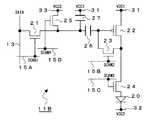
[第一回路例]
図2は、第一回路例に係る画素回路11Aの構成を示す回路図である。図2から明らかなように、本回路例に係る画素回路11Aは、有機EL素子20、5つのトランジスタ21〜25および2つのキャパシタ26,27を有する構成となっている。有機EL素子20は、発光層を含む有機層を第1、第2の電極で挟み込んだ構造となっている。
【0040】
第一乃至第五のトランジスタ21〜25は、ポリシリコンを活性層としたポリシリコン薄膜トランジスタ(TFT)である。本回路例では、これらトランジスタ21〜25のうち、第二のトランジスタ22としてPチャネルトランジスタを用い、それ以外のトランジスタ21,23〜25としてNチャネルトランジスタを用いた構成を採っている。
【0041】
第一のトランジスタ21は、ソース端が信号線13に、ゲート端が第一の走査線15Aにそれぞれ接続されている。第一のキャパシタ26は、一端(入力端)が第一のトランジスタ11のドレイン端に接続されている。第二のトランジスタ22は、ゲート端が第一のキャパシタ26の他端(出力端)に、ソース端が電源電圧VCC1(例えば、正電源電圧)の第一の電源線31にそれぞれ接続されている。
【0042】
第二のキャパシタ27は、一端が第一の電源線31に、他端が第二のトランジスタ22のゲート端にそれぞれ接続されている。第三のトランジスタ23は、ゲート端が第二の走査線15Bに、ソース端が第二のトランジスタ22のゲート端に、ドレイン端が第二のトランジスタ22のドレイン端にそれぞれ接続されている。第四のトランジスタ24は、ゲート端が第三の走査線15Cに、ソース端が第二のトランジスタ22のドレイン端にそれぞれ接続されている。
【0043】
第五のトランジスタ25は、ゲート端が第四の走査線15Dに、ソース端が電源電圧VCC3(例えば、正電源電圧)の第三の電源線33に、ドレイン端が第一のトランジスタ21のドレイン端(第一のキャパシタ26の一端)にそれぞれ接続されている。電源電圧VCC3は、電源電圧VCC1とは異なる電圧値となっている。有機EL素子20は、アノード端が第四のトランジスタ24のドレイン端に、カソード端が電源電圧VCC2(例えば、グランド電位)の第二の電源線32にそれぞれ接続されている。
【0044】
上記構成の第一回路例に係る画素回路11Aでは、同一データ線に接続された画素間で、データ書込期間としきい値電圧補正期間とが並行して存在するようにしている点を特徴としている。以下、データ書込期間およびしきい値電圧補正期間における各動作について、i行目の画素行の場合を例に挙げて図3のタイミングチャートを用いて説明する。図3のタイミングチャートにおいて、「補正」はしきい値電圧補正期間を、「書込」はデータ書込期間を、「保持」はデータ保持期間をそれぞれ表している。
【0045】
先ず、しきい値電圧補正期間において、スキャンドライバ14(図1参照)から第一の走査線15Aを介して与えられる走査パルスSCAN1(i) が“L”レベルであることによって第一のトランジスタ21がオフし、また第四の走査線15Dを介して与えられる走査パルスSCAN4(i) が“H”レベルであることによって第五のトランジスタ25がオンする。これにより、第一のキャパシタ26の入力端には、第3の電源線33から第五のトランジスタ25を通して電源電圧VCC3が固定電位Voとして供給される。
【0046】
このとき、第二の走査線15Bを介して与えられる走査パルスSCAN2(i) が“H”レベルであることによって第三のトランジスタ23がオンし、第三の走査線15Cを介して与えられる走査パルスSCAN3(i) が“L”レベルであることによって第四のトランジスタ24がオフする。これにより、第一のキャパシタ26は出力端側から第三のトランジスタ23のソース・ドレインを介して充電される。その際、しきい値電圧補正期間が十分に長ければ、第二のトランジスタ22のゲート・ソース間電圧は、トランジスタのしきい値電圧Vth(<0)に収束する。
【0047】
次のデータ書込期間に入ると、走査パルスSCAN1(i) が“H”レベルとなることで第一のトランジスタ21がオンし、走査パルスSCAN4(i) が“L”レベルとなることで第五のトランジスタ25がオフする。これにより、信号線13から第一のトランジスタ21を通してデータ電位Vo+Vdata(Vdata<0)が供給される。その際、走査パルスSCAN2(i) が“L”レベルであることによって第三のトランジスタ23はオフ状態にある。
【0048】
この第一回路例に係る画素回路11Aにおいても、先の式(2),(3)が同様に成り立つため、有機EL素子20に流れる電流Ioledは、トランジスタのしきい値電圧Vthに依存しないことがわかる。すなわち、画素毎の第二のトランジスタ22のしきい値電圧Vthが補正されていることがわかる。
【0049】
また同様に、しきい値電圧補正期間に必要な時間は、先の式(4),(5)で表される。しかし、本回路例に係る画素回路11Aにおいては、しきい値電圧補正期間における第一のキャパシタ26の入力端の信号線13との接続を第一のトランジスタ21によって制御し、電源線33との接続を第五のトランジスタ25によって制御する構成を採っている。したがって、しきい値電圧補正期間にはキャパシタ26の入力端を電源線33と接続して電源電圧VCC3を固定電位Voとして与え、データ書込期間にはキャパシタ26の入力端を信号線13に接続してデータ電位Vo+Vdataを与えることが可能となる。
【0050】
このように、キャパシタ26の入力端の接続先をしきい値電圧補正期間とデータ書込期間とで切替え制御することにより、ある画素が信号線13よりデータの書き込みを行っているデータ書込期間にあるのと並行して、別の画素を電源線33と接続することによってしきい値電圧補正期間にすることが可能である。また同時に、複数画素をしきい値電圧補正期間にすることも容易である。その結果、しきい値電圧補正期間として十分に長い期間を確保することが可能になる。
【0051】
具体的には、第一回路例に係る画素回路11Aにおいては、図3のタイミングチャートから明らかなように、ある画素行に注目した場合、1水平期間をデータ書込期間とするとともに、その直前の2水平期間をしきい値電圧補正期間としていることがわかる。また、ある時間に注目した場合、1つの画素(i行目)がデータ書込期間であるのと並行して、別の2つの画素(i+1行目とi+2行目)がしきい値電圧補正期間にあることがわかる。
【0052】
これにより、1水平期間内にしきい値電圧補正期間とデータ書込期間を持つ必要がなく、ディスプレイの高精細化と、十分に長いしきい値電圧補正期間の確保による均一性の良い表示画像を同時に実現することが可能になる。また、図3のタイミングチャートから明らかなように、信号線13は輝度データのみを順次供給すれば良いため、信号線13の駆動波形も容易であり、汎用的な液晶ディスプレイ等と同様の波形での駆動が可能である。したがって、信号線駆動回路であるデータドライバ12(図1参照)を簡単な回路構成にて実現できる。
【0053】
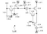
[第二回路例]
図4は、第二回路例に係る画素回路11Bの構成を示す回路図であり、図中、図2と同等部分には同一符号を付して示している。図4から明らかなように、本回路例に係る画素回路11Bも、第一回路例に係る画素回路11Aと同様に、有機EL素子20、5つのトランジスタ21〜25および2つのキャパシタ26,27を有する構成となっている。本回路例に係る画素回路11Bが、構成上、第一回路例に係る画素回路11Aと異なるのは、第二のキャパシタ27の接続位置の点だけである。
【0054】
以下に、各回路素子の接続関係について具体的に説明する。第一のトランジスタ21は、ソース端が信号線13に、ゲート端が第一の走査線15Aにそれぞれ接続されている。第一のキャパシタ26は、一端(入力端)が第一のトランジスタ11のドレイン端に接続されている。第二のトランジスタ22は、ゲート端が第一のキャパシタ26の他端(出力端)に、ソース端が電源電圧VCC1(例えば、正電源電圧)の第一の電源線31にそれぞれ接続されている。
【0055】
第二のキャパシタ27は、一端が第一の電源線31に、他端が第一のトランジスタ21のドレイン端(第一のキャパシタ26の他端)にそれぞれ接続されている。第三のトランジスタ23は、ゲート端が第二の走査線15Bに、ソース端が第二のトランジスタ22のゲート端に接続され、ドレイン端が第二のトランジスタ22のドレイン端にそれぞれ接続されている。第四のトランジスタ24は、ゲート端が第三の走査線15Cに、ソース端が第二のトランジスタ22のドレイン端にそれぞれ接続されている。
【0056】
第五のトランジスタ25は、ゲート端が第四の走査線15Dに、ソース端が電源電圧VCC3(例えば、正電源電圧)の第三の電源線33に、ドレイン端が第一のトランジスタ21のドレイン端(第一のキャパシタ26の一端)にそれぞれ接続されている。有機EL素子20は、アノード端が第四のトランジスタ24のドレイン端に、カソード端が電源電圧VCC2(例えば、グランド電位)の第二の電源線32にそれぞれ接続されている。
【0057】
上記構成の第二回路例に係る画素回路11Bにおいて、しきい値電圧補正、データ書き込みおよびデータ保持の各動作については第一回路例に係る画素回路11Aと基本的に同じである。また、第一回路例に係る画素回路11Aでは先の式(2),(3)が成り立つとしたが、第二回路例に係る画素回路11Bにおいては次式(6),(7)が成り立つ。
式(6),(7)から明らかなように、本回路例に係る画素回路11Bでも、有機EL素子20に流れる電流Ioledは、トランジスタのしきい値電圧Vthに依存しないことがわかる。すなわち、画素毎の第二のトランジスタ22のしきい値電圧Vthが補正されていることがわかる。また、データの入力電圧振幅Vdataが、そのまま第二のトランジスタ22のゲート電圧振幅となるため、信号線13の振幅を小さくすることが可能であり、低消費電力化が可能である。
【0059】
ところで、しきい値電圧補正型画素回路では、複数の走査線が必要となる。第一,第二回路例に係る画素回路11A,11Bでは、4本の走査線15A,15B,15C,15Dを用いている。しかし、このうち、第二の走査線15Bと第四の走査線15Dはしきい値電圧補正期間においてのみ第三,第五のトランジスタ23,5をオン駆動し、第三の走査線15Cはしきい値電圧補正期間においてのみ第四のトランジスタ24をオフ駆動する必要がある。したがって、これら第二,第三,第四の走査線15B,15C,15Dのうちの2本または3本全てを共通化することが可能である。
【0060】
なお、第三の走査線15Cを他の2本の走査線15B,15Dの少なくとも1本と共用するときには、第二,第三,第四の走査線15B,15C,15Dで駆動制御される第三,第四,第五のトランジスタ23,24,25のうち、第四のトランジスタ24については、第三,第五のトランジスタ23,25と逆導電型であることが必要となる。
【0061】
以下、これらの回路例に係る画素回路について説明する。以下に説明する各回路例に係る画素回路では、第二のキャパシタ27を第一のキャパシタ26の入力端側に接続した構成を採る第二回路例に係る画素回路11Bを基本形として説明する。ただし、第一回路例に係る画素回路11Aを基本形として同様に構成することも可能である。
【0062】
[第三回路例]
図5は、第三回路例に係る画素回路11Cの構成を示す回路図であり、図中、図4と同等部分については同一符号を付して示している。本回路例に係る画素回路11Cにおいては、第二の走査線15Bと第四の走査線15Dとを共通化し、共通の走査パルスSCAN2によって第三のトランジスタ23と第五のトランジスタ25とを駆動する構成を採っている。
【0063】
[第四回路例]
図6は、第四回路例に係る画素回路11Dの構成を示す回路図であり、図中、図4と同等部分については同一符号を付して示している。本回路例に係る画素回路11Dにおいては、第二の走査線15Bと第三の走査線15Cとを共通化し、共通の走査パルスSCAN2によって第三のトランジスタ23と第四のトランジスタ24とを駆動する構成を採っている。この場合、第三のトランジスタ23と第四のトランジスタ24としては逆導電型のものを用いる。本回路例では、第三のトランジスタ23としてNチャネルトランジスタを、第四のトランジスタ24としてPチャネルトランジスタをそれぞれ用いている。
【0064】
[第五回路例]
図7は、第四回路例に係る画素回路11Eの構成を示す回路図であり、図中、図4と同等部分については同一符号を付して示している。本回路例に係る画素回路11Eにおいては、第三の走査線15Cと第四の走査線15Dとを共通化し、共通の走査パルスSCAN4によって第四のトランジスタ24と第五のトランジスタ25とを駆動する構成を採っている。この場合、第四のトランジスタ24と第五のトランジスタ25としては逆導電型のものを用いる。本回路例では、第四のトランジスタ24としてPチャネルトランジスタを、第五のトランジスタ25としてNチャネルトランジスタをそれぞれ用いている。
【0065】
[第六回路例]
図8は、第六回路例に係る画素回路11Fの構成を示す回路図であり、図中、図4と同等部分については同一符号を付して示している。本回路例に係る画素回路11Fにおいては、第二の走査線15Bと第三の走査線15Cと第四の走査線15Dとを共通化し、共通の走査パルスSCAN2によって第三のトランジスタ23と第四のトランジスタ24と第五のトランジスタ25とを駆動する構成を採っている。この場合、第三,第五のトランジスタ23,25と第四のトランジスタ24としては逆導電型のものを用いる。本回路例では、第三,第五のトランジスタ23,25としてNチャネルトランジスタを、第四のトランジスタ24としてPチャネルトランジスタをそれぞれ用いている。
【0066】
上述した第三乃至第六回路例に係る画素回路11C〜11Fにおいて、しきい値電圧補正、データ書き込みおよびデータ保持の各動作については、第二回路例に係る画素回路11Bと同様である。したがって、しきい値電圧補正機能についても第二回路例に係る画素回路11Bと同様に実現されることになる。
【0067】
このように、第三乃至第六回路例に係る画素回路11C〜11Fにおいては、第二,第三,第四の走査線15B,15C,15Dのうちの2本または3本全てを共通化する構成を採っているため、走査線の削減による画素回路の小型化が可能となる。また、走査線の共通化により、スキャンドライバ14(図1参照)から出力する走査パルス数が少なくて済み、それに伴ってスキャンドライバ14の出力バッファ等の削減が可能になるため、スキャンドライバ14の構成の簡略化に寄与できる。
【0068】
なお、以上説明した第一乃至第六回路例11A〜11Fにおいて、第三の電源線33の電源電圧VCC3を第一の電源線31の電源電圧VCC1とは異なる電圧値に設定されることが前提となるが、その大小関係については特に規定されるものではない。
【0069】
[第七回路例]
図9は、第七回路例に係る画素回路11Gの構成を示す回路図であり、図中、図4と同等部分については同一符号を付して示している。本回路例に係る画素回路11Gにおいては、第一の電源線31と第三の電源線33とを共通化し、第一のキャパシタ26に対して固定電位Voとして電源電圧VCC1を与える構成を採っており、それ以外の構成については第二回路例に係る画素回路11Bと同様である。したがって、しきい値電圧補正機能についても第二回路例に係る画素回路11Bと同様に実現されることになる。
【0070】
このように、第一の電源線31と第三の電源線33とを共通化した構成を採ることにより、電源線数を削減できるため、しきい値電圧補正機能を第二回路例に係る画素回路11Bと同様に有しつつ、画素回路の小型化が可能となる。また、電源電圧が1つ減ることになるため、その分だけ電源回路の構成の簡略化に寄与できる。
【0071】
また、本回路例に係る画素回路11Gでは、第二回路例に係る画素回路11Bの回路構成を前提として、第一の電源線31と第三の電源線33とを共通化するとしたが、第一の電源線31と第三の電源線33とを共通化した上でさらに、第三回路例に係る画素回路11Cと同様に、第二の走査線15Bと第四の走査線15Dとを共通化する構成を採ることも可能である。
【0072】
なお、以上説明した各回路例11A〜11Gにおいて、第一乃至第五のトランジスタ21〜25のソース端が第一電極端に、ドレイン端が第二電極端にそれぞれ対応するものとする。第一乃至第五のトランジスタ21〜25の導電型については、上記各回路例のものに限られるものではなく、適宜逆導電型のものに変更することが可能である。
【0073】
次に、信号線13の電位の決定方法について説明する。2トランジスタの従来例に係る画素回路(図12)および第二回路例に係る画素回路11B(図4)における入力データとそのときの信号線103,13の電位との関係を図10に示す。
【0074】
従来例に係る画素回路では、信号線103の電位は電源電圧VCC1に依存するため、電源電圧VCC1が大きい場合、信号線103の電位も高くなる傾向があった。これに対して、第二回路例に係る画素回路11Bでは、式(7)が成り立つことから、輝度データが電源電圧VCC3との差分によって決定される。したがって、電源電圧VCC3を電源電圧VCC1と独立に小さく設定することが可能である。
【0075】
そして、電源電圧VCC3を電源電圧VCC1に対して極めて小さく設定することにより、信号線駆動回路であるデータドライバ12の低電圧化を図ることができるため、低消費電力化が可能になる。また、現実の画素回路では、配線間やトランジスタに多くの寄生容量が存在するため、正確な輝度データを供給することが難しい。そこで、電源電圧VCC3を可変とすることにより、正確な階調表示を行うための微調整として用いることも可能である。このことは、第三乃至第六回路例に係る画素回路11C〜11Fについても同様である。
【0076】
なお、上記実施形態においては、画素の表示素子として有機EL素子を、能動素子としてポリシリコン薄膜トランジスタをそれぞれ用い、ポリシリコン薄膜トランジスタを形成した基板上に有機EL素子を形成してなるアクティブマトリクス型有機ELディスプレイに適用する場合を例に採って説明したが、本発明はアクティブマトリクス型有機ELディスプレイへの適用に限られるものではなく、画素毎に表示素子を有し、画素内に輝度データを保持することが可能なアクティブマトリクス型表示装置全般に適用可能である。
【0077】
【発明の効果】
以上説明したように、本発明によれば、しきい値電圧の補正に必要となる固定電位を、信号線とは異なる電源線から供給するようにしたことで、1水平期間をデータ書込期間として設定できるとともに、その直前にしきい値電圧補正期間として任意の期間を設定できるため、しきい値電圧補正期間として十分に長い期間を確保できる。これにより、トランジスタのしきい値電圧ばらつきを画素毎に確実に補正できるため、輝度の均一性を向上できるとともに、ディスプレイの高精細化が可能となる。
【0078】
また、信号線駆動回路からは信号線に対して、従来技術のようにしきい値補正期間で固定電位、データ書込期間でデータ電位+固定電位をそれぞれ供給する必要がなくなり、データ電位のみを順次供給すれば良いことになるため、信号線駆動回路の構成を簡略化でき、しかも固定電位が無くなる分だけ信号線駆動回路の電源電圧を低電圧化できるため、ディスプレイ全体の低消費電力化を図ることができる。
【図面の簡単な説明】
【図1】本発明の一実施形態に係るアクティブマトリクス型表示装置の構成の概略を示すブロック図である。
【図2】第一回路例に係る画素回路の構成を示す回路図である。
【図3】第一回路例に係る画素回路の動作説明のためのタイミングチャートである。
【図4】第二回路例に係る画素回路の構成を示す回路図である。
【図5】第三回路例に係る画素回路の構成を示す回路図である。
【図6】第四回路例に係る画素回路の構成を示す回路図である。
【図7】第五回路例に係る画素回路の構成を示す回路図である。
【図8】第六回路例に係る画素回路の構成を示す回路図である。
【図9】第七回路例に係る画素回路の構成を示す回路図である。
【図10】入力データとそのときの信号線の電位との関係を示す図である。
【図11】最も簡単なアクティブマトリクス型有機ELディスプレイの構成の概略を示すブロック図である。
【図12】2トランジスタの画素回路の構成を示す回路図である。
【図13】従来例に係る画素回路の構成を示す回路図である。
【図14】従来例に係る画素回路の動作説明のためのタイミングチャートである。
【符号の説明】
11,11A,11B,11C,11D,11E,11F,11G…画素回路(画素)、12…データドライバ(信号線駆動回路)、13…信号線、14…スキャンドライバ(走査線駆動回路)、15A…第一の走査線、15B…第二の走査線、15C…第三の走査線、15D…第四の走査線、21…第一のトランジスタ、22…第二のトランジスタ、23…第三のトランジスタ、24…第四のトランジスタ、25…第五のトランジスタ、26…第一のキャパシタ、27…第二のキャパシタ、31…第一の電源線、32…第二の電源線、33…第三の電源線[0001]
BACKGROUND OF THE INVENTION
The present invention relates to an active matrix display device in which pixels (pixel circuits) having display elements are arranged in a matrix, and image data is written and displayed by scanning lines and signal lines.In placeIn particular, an active matrix organic EL display device using, for example, an organic electroluminescence (EL) element as a display elementIn placeRelated.
[0002]
[Prior art]
In an active matrix display device, an electro-optical element such as a liquid crystal cell or an organic EL element is used as a display element of a pixel. Among them, the organic EL element has a structure in which a layer made of an organic material, that is, an organic layer is sandwiched between electrodes. In this organic EL element, by applying a voltage to the element, electrons from the cathode and holes from the anode are injected into the organic layer. As a result, the electrons and holes are recombined to generate light. This organic EL element has the following features.
[0003]
1) Low voltage drive of 10V or less, hundreds to tens of thousands cd / m2 Therefore, low power consumption can be achieved.
2) Since it is a self-luminous element, the contrast of the image is high and the response speed is fast, so that the visibility is good and it is also suitable for displaying moving images.
3) It is an all solid state element with a simple structure, and the element can be made highly reliable and thin.
An organic EL display device using an organic EL element having these features as a pixel display element (hereinafter referred to as an organic EL display) is considered promising as a next-generation flat panel display.
[0004]
By the way, as a driving method of the organic EL display, there are a simple matrix method and an active matrix method. Among these methods, the active matrix method has the following features.
1) An active matrix system that can hold light emission of an organic EL element in each pixel for one frame period is suitable for high definition and high luminance of an organic EL display.
2) Since a peripheral circuit using a thin film transistor can be formed on a substrate (panel), the interface with the outside of the panel can be simplified and the function of the panel can be enhanced.
[0005]
In this active matrix organic EL display, a polysilicon thin film transistor (TFT) using polysilicon as an active layer is generally used as a transistor which is an active element. This is because the polysilicon TFT has a high driving capability and can be designed to have a small pixel size, which is advantageous for high definition. While having such features, it is well known that polysilicon TFTs have large variations in characteristics.
[0006]
Therefore, in the case of using a polysilicon TFT, it is a big problem in an active matrix type organic EL display using a polysilicon TFT to suppress the characteristic variation and to compensate for the TFT characteristic variation in a circuit. This is due to the following reason. That is, in a liquid crystal display using a liquid crystal cell as a pixel display element, the luminance data of each pixel is controlled by a voltage value, whereas in an organic EL display, the luminance data of each pixel is controlled by a current value. It is because the structure to control is taken.
[0007]
Here, an outline of the active matrix organic EL display will be described. FIG. 11 shows a schematic configuration of the simplest active matrix organic EL display, and FIG. 12 shows a circuit configuration of the pixel circuit (see, for example, Patent Document 1). In the active matrix organic EL display, m × n pixels 101 are arranged in a matrix, and signal lines 103-1 to 103-for m columns driven by the data driver 102 with respect to the matrix arrangement of the pixels 101. In this configuration, m is arranged for each pixel column, and n rows of scanning lines 105-1 to 105-n driven by the
[0008]
Further, as is apparent from FIG. 12, the pixel (pixel circuit) 101 has an organic EL element 110, first and second transistors 111 and 112, and a capacitor 113. Here, an N-channel transistor is used as the first transistor 111, and a P-channel transistor is used as the second transistor 112.
[0009]
The first transistor 111 has a source terminal connected to the signal line 103 (103-1 to 103-m) and a gate terminal connected to the scanning line 105 (105-1 to 105-n). One end of the capacitor 113 is connected to the first power supply line 121 of the power supply voltage VCC1 (for example, positive power supply voltage), and the other end is connected to the drain end of the first transistor 111. The second transistor 112 has a source terminal connected to the first power supply line 121 and a gate terminal connected to the drain terminal of the first transistor 111. The organic EL element 110 has an anode end connected to the drain end of the second transistor 112 and a cathode end connected to the second power supply line 122 of the power supply voltage VCC2 (for example, ground potential).
[0010]
In the pixel circuit having the above structure, in a pixel to which luminance data is written, a pixel row including the pixel is selected via the
[0011]
Thereby, the second transistor 112 drives the organic EL element 110 with current according to the retained data. At this time, gradation representation of the organic EL element 110 is performed by modulating the gate-source voltage Vdata (<0) of the second transistor 112 held by the capacitor 113.
[0012]
In general, the luminance Loled of the organic EL element is proportional to the current Ioled flowing through the element. Therefore, the following equation is established between the luminance Loled of the organic EL element and the current Ioled.
In Equation (1), k = 1/2 · μ · Cox · W / L. Here, μ is the carrier mobility of the second transistor 112, Cox is the gate capacitance per unit area of the second transistor 112, W is the gate width of the second transistor 112, and L is the second transistor 112. The gate length. Therefore, it can be seen that the variation in mobility μ and threshold voltage Vth (<0) of the second transistor 112 directly affects the luminance variation of the organic EL element.
[0014]
On the other hand, a threshold voltage correction type pixel circuit has been devised as a pixel circuit capable of compensating for the threshold voltage Vth in which luminance variation is likely to cause a problem (see, for example, Patent Document 2).
[0015]
FIG. 13 is a circuit diagram showing a configuration of a threshold voltage correction type pixel circuit according to a conventional example. In FIG. 13, the same parts as those in FIG. 12 are denoted by the same reference numerals. As can be seen from FIG. 13, the threshold voltage correction type pixel circuit according to this conventional example has an organic EL element 110, four
[0016]
The first transistor 111 has a source terminal connected to the
[0017]
The
[0018]
Next, the circuit operation of the threshold voltage correction type pixel circuit according to the conventional example having the above configuration will be described with reference to the timing chart of FIG. This timing chart shows the timing relationship at the time of driving the pixel circuits in the i-th and i + 1-th rows. In the timing chart of FIG. 14, “correction” represents a threshold voltage correction period, “write” represents a data write period, and “hold” represents a data hold period.
[0019]
In the operation of this pixel circuit, a threshold voltage correction period exists prior to the data writing period. In this threshold voltage correction period, the first transistor 111 is turned on when the scan pulse SCAN1 applied via the first scan line 105A becomes high level (hereinafter referred to as “H” level). A fixed potential Vo is supplied to the
[0020]
In this state, the first capacitor 116 whose one end is at the fixed potential Vo is charged via the source / drain of the
[0021]
In the next data writing period, since the scan pulse SCAN1 is maintained at the “H” level, the first transistor 111 is in an ON state, and the data potential Vo + Vdata (Vdata <0) is supplied from the signal line 102. Is done. At this time, since the scan pulse SCAN2 is at the “L” level, the
[0022]
Here, assuming that the gate capacitance, parasitic capacitance, and the like of the transistor are ignored, the gate-source voltage Vgs of the second transistor 112 is expressed by the following equation.
Vgs = Vth + C1 / (C1 + C2) · Vdata (2)
C1 and C2 represent the capacitance values of the first and second capacitors 116 and 113, respectively.
[0023]
By using the equation (2), the current Ioled flowing through the organic EL element 110 is expressed as the following equation.
As is clear from Expression (3), it can be seen that the current Ioled flowing through the organic EL element 110 does not depend on the threshold voltage Vth of the second transistor 112. That is, it can be seen that the threshold voltage Vth of the second transistor 112 for each pixel is corrected by using the threshold voltage correction type pixel circuit according to the conventional example. This means that the variation in the threshold voltage Vth of the second transistor 112 does not affect the luminance variation of the organic EL element 110.
[0025]
[Patent Document 1]
JP-A-8-234683
[Patent Document 2]
US Pat. No. 6,229,506
[0026]
[Problems to be solved by the invention]
By the way, in the threshold voltage correction type pixel circuit according to the conventional example described above, in the threshold voltage correction period, the second transistor 112 changes as the source-gate voltage changes toward the threshold voltage Vth. Since it gradually approaches the OFF state and the operation becomes slow with this, it takes time for the source-gate voltage of the second transistor 112 to converge to the threshold voltage Vth. Therefore, a sufficiently long time is required as the threshold voltage correction period.
[0027]
A differential equation related to the gate voltage of the second transistor 112 during the threshold voltage correction period is expressed as the following equation.
k · {Vgs (t) −Vth}2 = −Cs · dVgs / dt (4)
In Equation (4), as a sufficient threshold voltage correction period, consider the time during which the current is ½ that of the minimum luminance.
[0028]
The current value at the maximum luminance of the organic EL element 110 is Imax, the initial value of the gate-source voltage Vgs of the second transistor 112 is Vinit, and the holding capacity of the gate voltage of the second transistor 112 (mainly the second voltage). Capacitor 113 has capacitance C1) Cs, the number of gradations n, and the gate-source voltage Vgs that gives the current value Imax at the maximum luminance is Vgs = ΔV + Vth. The time required to become (n-1) is expressed by the following equation.
t = Cs · ΔV / Imax {√ (2n−2) −ΔV / Vinit (5)
[0029]
Here, as an example of numerical values, Cs = 1 [pF], n = 64, ΔV = 4, Imax = 1 [μA], and the second term is t = 45 [μs] considering a sufficiently small case. . On the other hand, in the case of resolution (graphics display standard) VGA, 480 scanning lines, and frame frequency of 60 Hz, one horizontal period is about 30 μs, and it is difficult to end the threshold voltage period between one horizontal period. Recognize.
[0030]
As described above, since a VGA class display requires a time of several μs to several tens of μs as a sufficient threshold voltage correction period, the threshold voltage correction period and the data writing period are continued within one horizontal period. It is difficult to do. In other words, the threshold voltage correction type pixel circuit according to the conventional example cannot be applied to the VGA class organic EL display. It can also be seen that as the display becomes higher in definition, one horizontal period becomes shorter in inverse proportion to the number of scanning lines, so that it becomes more difficult to secure a sufficient threshold voltage correction period.
[0031]
In the threshold voltage correction pixel circuit according to the conventional example, the
[0032]
The present invention has been made in view of the above problems, and an object of the present invention is to improve the uniformity of a display image by using a threshold voltage correction type pixel circuit and to increase the length of one horizontal period. Regardless of the active matrix type display device that enables high definition by ensuring a sufficient threshold voltage correction period.PlaceIt is to provide.
[0033]
[Means for Solving the Problems]
An active matrix display device according to the present invention includes a plurality of pixel circuits arranged in a matrix, signal lines wired for each column with respect to the matrix arrangement of the pixel circuits, and rows with respect to the matrix arrangement of the pixel circuits. 1st, 2nd, 3rd and 4th scanning lines wired every time, each of the pixel circuits, the gate end to the first scanning line, the first electrode end to the signal line, respectively A first transistor connected, a first capacitor having one end connected to the second electrode end of the first transistor, and a second capacitor having one end connected to the other end or one end of the first capacitor. A capacitor, a second transistor having a gate terminal connected to the other end of the first capacitor, a first electrode terminal connected to the first power line, and a gate terminal connected to the second scanning line; The electrode end is A third transistor having a second electrode terminal connected to the second electrode terminal of the second transistor, a gate terminal connected to the third scanning line, and a first electrode terminal connected to the first electrode terminal A fourth transistor connected to the second electrode end of each of the two transistors, a gate end at the fourth scanning line, a first electrode end at the third power supply line, and a second electrode end at the first electrode And a display element connected between the second electrode end of the fourth transistor and the second power supply line. Yes.
[0034]
In the active matrix display device having the above-described configuration,The third transistor and the fourth transistor are of opposite conductivity type, and the second scanning line and the third scanning line are common, or the fourth transistor and the fifth transistor are The third scanning line and the fourth scanning line are common, or the third transistor, the fifth transistor and the fourth transistor are of the reverse conductivity type, The second scanning line, the third scanning line, and the fourth scanning line are common. Alternatively, the power supply voltage of the third power supply line is lower than the power supply voltage of the first power supply line, or the power supply voltage of the third power supply line is variable.
Also,The first and fourth transistors are turned off, the third and fifth transistors are turned on, and the threshold voltage of the second transistor is corrected for each pixel.,FourthThe transistors are turned on, the third and fifth transistors are turned off, and the display line is driven to write display data to the pixels. In the period for correcting the threshold voltage of the second transistor, the fifth transistor supplies the first capacitor with the power supply voltage of the third power supply line as a fixed potential.
[0035]
In this way, by supplying a fixed potential necessary for correcting the threshold voltage from a power supply line different from the signal line, display data is written from the signal line to another pixel in parallel with a certain pixel. Thus, the threshold voltage can be corrected. Thus, when attention is paid to a certain pixel row, one horizontal period can be set as a data writing period, and an arbitrary period can be set as a threshold voltage correction period immediately before that, so that the threshold voltage correction period is sufficient. A long period can be secured.
[0036]
DETAILED DESCRIPTION OF THE INVENTION
Hereinafter, embodiments of the present invention will be described in detail with reference to the drawings. FIG. 1 is a block diagram showing an outline of the configuration of an active matrix display device according to an embodiment of the present invention. In the present embodiment, for example, an organic EL element is used as a display element of a pixel, a polysilicon thin film transistor (TFT) is used as an active element, and the organic EL element is formed on a substrate on which the thin film transistor is formed. The case where it is applied to a display will be described as an example.
[0037]
In FIG. 1, each of m × n pixels (pixel circuits) 11 has an organic EL element as a display element, and is arranged in a matrix. For the matrix arrangement of the
[0038]
In the active matrix organic EL display having the above configuration, the present invention is characterized by a specific circuit configuration and circuit operation of the pixel 11 (pixel circuit). Hereinafter, some specific circuit examples of the
[0039]
[First circuit example]
FIG. 2 is a circuit diagram showing a configuration of a pixel circuit 11A according to the first circuit example. As apparent from FIG. 2, the
[0040]
The first to
[0041]
The
[0042]
The
[0043]
The
[0044]
The pixel circuit 11A according to the first circuit example having the above configuration is characterized in that a data writing period and a threshold voltage correction period exist in parallel between pixels connected to the same data line. Yes. Hereinafter, each operation in the data writing period and the threshold voltage correction period will be described with reference to the timing chart of FIG. 3 taking the case of the i-th pixel row as an example. In the timing chart of FIG. 3, “correction” represents a threshold voltage correction period, “write” represents a data write period, and “hold” represents a data hold period.
[0045]
First, in the threshold voltage correction period, the
[0046]
At this time, when the scanning pulse SCAN2 (i) applied through the
[0047]
In the next data writing period, the scan pulse SCAN1 (i) becomes “H” level to turn on the
[0048]
Also in the pixel circuit 11A according to the first circuit example, since the previous expressions (2) and (3) are similarly established, the current Ioled flowing through the
[0049]
Similarly, the time required for the threshold voltage correction period is expressed by the above equations (4) and (5). However, in the pixel circuit 11A according to this circuit example, the connection with the
[0050]
In this way, the data writing period in which a pixel is writing data from the
[0051]
Specifically, in the pixel circuit 11A according to the first circuit example, as is clear from the timing chart of FIG. 3, when attention is paid to a certain pixel row, one horizontal period is set as the data writing period and immediately before that. It can be seen that the two horizontal periods are the threshold voltage correction period. When attention is paid to a certain time, another two pixels (i + 1th row and i + 2th row) are corrected for threshold voltage in parallel with one pixel (ith row) being in the data writing period. You can see that it is in the period.
[0052]
As a result, it is not necessary to have a threshold voltage correction period and a data writing period within one horizontal period, and a display image with good uniformity can be obtained by increasing the definition of the display and ensuring a sufficiently long threshold voltage correction period. It can be realized at the same time. Further, as apparent from the timing chart of FIG. 3, since the
[0053]
[Second circuit example]
FIG. 4 is a circuit diagram showing the configuration of the pixel circuit 11B according to the second circuit example. In FIG. 4, the same parts as those in FIG. As is apparent from FIG. 4, the pixel circuit 11B according to this circuit example includes the
[0054]
Below, the connection relationship of each circuit element is demonstrated concretely. The
[0055]
The
[0056]
The
[0057]
In the pixel circuit 11B according to the second circuit example configured as described above, the threshold voltage correction, data writing, and data holding operations are basically the same as those of the pixel circuit 11A according to the first circuit example. In the pixel circuit 11A according to the first circuit example, the previous expressions (2) and (3) are satisfied. However, in the pixel circuit 11B according to the second circuit example, the following expressions (6) and (7) are satisfied. .
As apparent from the equations (6) and (7), it can be seen that also in the pixel circuit 11B according to this circuit example, the current Ioled flowing through the
[0059]
Incidentally, a threshold voltage correction type pixel circuit requires a plurality of scanning lines. In the pixel circuits 11A and 11B according to the first and second circuit examples, four
[0060]
When the third scanning line 15C is shared with at least one of the other two scanning
[0061]
Hereinafter, pixel circuits according to these circuit examples will be described. In the pixel circuit according to each circuit example described below, the pixel circuit 11B according to the second circuit example having a configuration in which the
[0062]
[Third circuit example]
FIG. 5 is a circuit diagram showing a configuration of a pixel circuit 11C according to the third circuit example. In FIG. 5, the same parts as those in FIG. 4 are denoted by the same reference numerals. In the pixel circuit 11C according to this circuit example, the
[0063]
[Fourth circuit example]
FIG. 6 is a circuit diagram showing the configuration of the pixel circuit 11D according to the fourth circuit example. In FIG. 6, the same parts as those in FIG. 4 are denoted by the same reference numerals. In the pixel circuit 11D according to this circuit example, the
[0064]
[Fifth circuit example]
FIG. 7 is a circuit diagram showing a configuration of a pixel circuit 11E according to the fourth circuit example. In FIG. 7, the same parts as those in FIG. 4 are denoted by the same reference numerals. In the pixel circuit 11E according to this circuit example, the third scanning line 15C and the fourth scanning line 15D are shared, and the
[0065]
[Sixth circuit example]
FIG. 8 is a circuit diagram showing the configuration of the pixel circuit 11F according to the sixth circuit example. In FIG. 8, the same parts as those in FIG. 4 are denoted by the same reference numerals. In the pixel circuit 11F according to this circuit example, the
[0066]
In the pixel circuits 11C to 11F according to the third to sixth circuit examples described above, operations of threshold voltage correction, data writing, and data holding are the same as those of the pixel circuit 11B according to the second circuit example. Therefore, the threshold voltage correction function is also realized in the same manner as the pixel circuit 11B according to the second circuit example.
[0067]
As described above, in the pixel circuits 11C to 11F according to the third to sixth circuit examples, two or all of the second, third, and
[0068]
In the first to sixth circuit examples 11A to 11F described above, it is assumed that the power supply voltage VCC3 of the third power supply line 33 is set to a voltage value different from the power supply voltage VCC1 of the first
[0069]
[Seventh circuit example]
FIG. 9 is a circuit diagram showing a configuration of a pixel circuit 11G according to the seventh circuit example. In FIG. 9, the same parts as those in FIG. 4 are denoted by the same reference numerals. In the pixel circuit 11G according to this circuit example, the first
[0070]
Thus, since the number of power supply lines can be reduced by adopting a configuration in which the first
[0071]
In the pixel circuit 11G according to this circuit example, the first
[0072]
In each of the circuit examples 11A to 11G described above, the source ends of the first to
[0073]
Next, a method for determining the potential of the
[0074]
In the pixel circuit according to the conventional example, since the potential of the
[0075]
Then, by setting the power supply voltage VCC3 to be very small with respect to the power supply voltage VCC1, it is possible to reduce the voltage of the
[0076]
In the above embodiment, an organic EL element is used as a display element of a pixel, a polysilicon thin film transistor is used as an active element, and the organic EL element is formed on a substrate on which the polysilicon thin film transistor is formed. The case where the present invention is applied to a display has been described as an example. However, the present invention is not limited to application to an active matrix organic EL display, and has a display element for each pixel and holds luminance data in the pixel. The present invention can be applied to all active matrix display devices that can be used.
[0077]
【The invention's effect】
As described above, according to the present invention, the fixed potential necessary for correcting the threshold voltage is supplied from the power supply line different from the signal line, so that one horizontal period is the data writing period. Since an arbitrary period can be set immediately before the threshold voltage correction period, a sufficiently long period can be secured as the threshold voltage correction period. Thereby, the threshold voltage variation of the transistor can be reliably corrected for each pixel, so that the uniformity of luminance can be improved and the display can be made high definition.
[0078]
Further, it is not necessary to supply a fixed potential in the threshold correction period and a data potential + fixed potential in the data writing period from the signal line driving circuit to the signal line as in the conventional technique, and only the data potential is sequentially applied. Since the power supply voltage of the signal line driver circuit can be simplified and the power supply voltage of the signal line driver circuit can be reduced by the amount of no fixed potential, the power consumption of the entire display can be reduced. be able to.
[Brief description of the drawings]
FIG. 1 is a block diagram showing an outline of a configuration of an active matrix display device according to an embodiment of the present invention.
FIG. 2 is a circuit diagram illustrating a configuration of a pixel circuit according to a first circuit example.
FIG. 3 is a timing chart for explaining the operation of the pixel circuit according to the first circuit example;
FIG. 4 is a circuit diagram illustrating a configuration of a pixel circuit according to a second circuit example.
FIG. 5 is a circuit diagram illustrating a configuration of a pixel circuit according to a third circuit example.
FIG. 6 is a circuit diagram illustrating a configuration of a pixel circuit according to a fourth circuit example.
FIG. 7 is a circuit diagram showing a configuration of a pixel circuit according to a fifth circuit example.
FIG. 8 is a circuit diagram showing a configuration of a pixel circuit according to a sixth circuit example.
FIG. 9 is a circuit diagram illustrating a configuration of a pixel circuit according to a seventh circuit example.
FIG. 10 is a diagram illustrating a relationship between input data and a potential of a signal line at that time.
FIG. 11 is a block diagram showing an outline of the configuration of the simplest active matrix type organic EL display.
FIG. 12 is a circuit diagram illustrating a configuration of a two-transistor pixel circuit.
FIG. 13 is a circuit diagram illustrating a configuration of a pixel circuit according to a conventional example.
FIG. 14 is a timing chart for explaining the operation of a pixel circuit according to a conventional example.
[Explanation of symbols]
11, 11A, 11B, 11C, 11D, 11E, 11F, 11G ... Pixel circuit (pixel), 12 ... Data driver (signal line drive circuit), 13 ... Signal line, 14 ... Scan driver (scan line drive circuit), 15A ... first scanning line, 15B ... second scanning line, 15C ... third scanning line, 15D ... fourth scanning line, 21 ... first transistor, 22 ... second transistor, 23 ...
Claims (3)
Translated fromJapanese前記画素回路のマトリクス配列に対して列毎に配線された信号線と、
前記画素回路のマトリクス配列に対して行毎に配線された第一,第二,第三および第四の走査線とを備え、
前記画素回路の各々が、
ゲート端が前記第一の走査線に、第一電極端が前記信号線にそれぞれ接続された第一のトランジスタと、
一端が前記第一のトランジスタの第二電極端に接続された第一のキャパシタと、
一端が前記第一のキャパシタの他端または一端に接続された第二のキャパシタと、
ゲート端が前記第一のキャパシタの他端に、第一電極端が第一の電源線にそれぞれ接続された第二のトランジスタと、
ゲート端が前記第二の走査線に、第一電極端が前記第二のトランジスタのゲート端に、第二電極端が前記第二のトランジスタの第二電極端にそれぞれ接続された第三のトランジスタと、
ゲート端が前記第三の走査線に、第一電極端が前記第二のトランジスタの第二電極端にそれぞれ接続された第四のトランジスタと、
ゲート端が前記第四の走査線に、第一電極端が第三の電源線に、第二電極端が前記第一のトランジスタの第二電極端にそれぞれ接続された第五のトランジスタと、
前記第四のトランジスタの第二電極端と第二の電源線との間に接続された表示素子とを有し、
前記第三のトランジスタと前記第四のトランジスタとが逆導電型であり、前記第二の走査線と前記第三の走査線とが共通である
ことを特徴とするアクティブマトリクス型表示装置。A plurality of pixel circuits arranged in a matrix;
Signal lines wired for each column with respect to the matrix arrangement of the pixel circuits;
First, second, third and fourth scanning lines wired for each row with respect to the matrix arrangement of the pixel circuit,
Each of the pixel circuits
A first transistor having a gate end connected to the first scanning line and a first electrode end connected to the signal line;
A first capacitor having one end connected to the second electrode end of the first transistor;
A second capacitor having one end connected to the other end or one end of the first capacitor;
A second transistor having a gate terminal connected to the other end of the first capacitor and a first electrode terminal connected to the first power supply line;
A third transistor having a gate terminal connected to the second scanning line, a first electrode terminal connected to the gate terminal of the second transistor, and a second electrode terminal connected to the second electrode terminal of the second transistor; When,
A fourth transistor having a gate terminal connected to the third scanning line and a first electrode terminal connected to the second electrode terminal of the second transistor;
A fifth transistor having a gate end connected to the fourth scanning line, a first electrode end connected to a third power supply line, and a second electrode end connected to the second electrode end of the first transistor;
A display element connected between the second electrode end of the fourth transistor and a second power supply line;
The active matrix display device, wherein the third transistor and the fourth transistor are of a reverse conductivity type, and the second scanning line and the third scanning line are common.
前記画素回路のマトリクス配列に対して列毎に配線された信号線と、
前記画素回路のマトリクス配列に対して行毎に配線された第一,第二,第三および第四の走査線とを備え、
前記画素回路の各々が、
ゲート端が前記第一の走査線に、第一電極端が前記信号線にそれぞれ接続された第一のトランジスタと、
一端が前記第一のトランジスタの第二電極端に接続された第一のキャパシタと、
一端が前記第一のキャパシタの他端または一端に接続された第二のキャパシタと、
ゲート端が前記第一のキャパシタの他端に、第一電極端が第一の電源線にそれぞれ接続された第二のトランジスタと、
ゲート端が前記第二の走査線に、第一電極端が前記第二のトランジスタのゲート端に、第二電極端が前記第二のトランジスタの第二電極端にそれぞれ接続された第三のトランジスタと、
ゲート端が前記第三の走査線に、第一電極端が前記第二のトランジスタの第二電極端にそれぞれ接続された第四のトランジスタと、
ゲート端が前記第四の走査線に、第一電極端が第三の電源線に、第二電極端が前記第一のトランジスタの第二電極端にそれぞれ接続された第五のトランジスタと、
前記第四のトランジスタの第二電極端と第二の電源線との間に接続された表示素子とを有し、
前記第四のトランジスタと前記第五のトランジスタとが逆導電型であり、前記第三の走査線と前記第四の走査線とが共通である
ことを特徴とするアクティブマトリクス型表示装置。A plurality of pixel circuits arranged in a matrix;
Signal lines wired for each column with respect to the matrix arrangement of the pixel circuits;
First, second, third and fourth scanning lines wired for each row with respect to the matrix arrangement of the pixel circuit,
Each of the pixel circuits
A first transistor having a gate end connected to the first scanning line and a first electrode end connected to the signal line;
A first capacitor having one end connected to the second electrode end of the first transistor;
A second capacitor having one end connected to the other end or one end of the first capacitor;
A second transistor having a gate terminal connected to the other end of the first capacitor and a first electrode terminal connected to the first power supply line;
A third transistor having a gate terminal connected to the second scanning line, a first electrode terminal connected to the gate terminal of the second transistor, and a second electrode terminal connected to the second electrode terminal of the second transistor; When,
A fourth transistor having a gate terminal connected to the third scanning line and a first electrode terminal connected to the second electrode terminal of the second transistor;
A fifth transistor having a gate end connected to the fourth scanning line, a first electrode end connected to a third power supply line, and a second electrode end connected to the second electrode end of the first transistor;
A display element connected between the second electrode end of the fourth transistor and a second power supply line;
The active matrix display device, wherein the fourth transistor and the fifth transistor are of a reverse conductivity type, and the third scanning line and the fourth scanning line are common.
前記画素回路のマトリクス配列に対して列毎に配線された信号線と、
前記画素回路のマトリクス配列に対して行毎に配線された第一,第二,第三および第四の走査線とを備え、
前記画素回路の各々が、
ゲート端が前記第一の走査線に、第一電極端が前記信号線にそれぞれ接続された第一のトランジスタと、
一端が前記第一のトランジスタの第二電極端に接続された第一のキャパシタと、
一端が前記第一のキャパシタの他端または一端に接続された第二のキャパシタと、
ゲート端が前記第一のキャパシタの他端に、第一電極端が第一の電源線にそれぞれ接続された第二のトランジスタと、
ゲート端が前記第二の走査線に、第一電極端が前記第二のトランジスタのゲート端に、第二電極端が前記第二のトランジスタの第二電極端にそれぞれ接続された第三のトランジスタと、
ゲート端が前記第三の走査線に、第一電極端が前記第二のトランジスタの第二電極端にそれぞれ接続された第四のトランジスタと、
ゲート端が前記第四の走査線に、第一電極端が第三の電源線に、第二電極端が前記第一のトランジスタの第二電極端にそれぞれ接続された第五のトランジスタと、
前記第四のトランジスタの第二電極端と第二の電源線との間に接続された表示素子とを有し、
前記第三のトランジスタおよび前記第五のトランジスタと前記第四のトランジスタとが逆導電型であり、前記第二の走査線と前記第三の走査線と前記第四の走査線とが共通である
ことを特徴とするアクティブマトリクス型表示装置。A plurality of pixel circuits arranged in a matrix;
Signal lines wired for each column with respect to the matrix arrangement of the pixel circuits;
First, second, third and fourth scanning lines wired for each row with respect to the matrix arrangement of the pixel circuit,
Each of the pixel circuits
A first transistor having a gate end connected to the first scanning line and a first electrode end connected to the signal line;
A first capacitor having one end connected to the second electrode end of the first transistor;
A second capacitor having one end connected to the other end or one end of the first capacitor;
A second transistor having a gate terminal connected to the other end of the first capacitor and a first electrode terminal connected to the first power supply line;
A third transistor having a gate terminal connected to the second scanning line, a first electrode terminal connected to the gate terminal of the second transistor, and a second electrode terminal connected to the second electrode terminal of the second transistor; When,
A fourth transistor having a gate terminal connected to the third scanning line and a first electrode terminal connected to the second electrode terminal of the second transistor;
A fifth transistor having a gate end connected to the fourth scanning line, a first electrode end connected to a third power supply line, and a second electrode end connected to the second electrode end of the first transistor;
A display element connected between the second electrode end of the fourth transistor and a second power supply line;
The third transistor, the fifth transistor, and the fourth transistor are of a reverse conductivity type, and the second scanning line, the third scanning line, and the fourth scanning line are common. An active matrix display device characterized by the above.
Priority Applications (4)
| Application Number | Priority Date | Filing Date | Title |
|---|---|---|---|
| JP2002298428AJP3832415B2 (en) | 2002-10-11 | 2002-10-11 | Active matrix display device |
| US10/667,596US7057588B2 (en) | 2002-10-11 | 2003-09-23 | Active-matrix display device and method of driving the same |
| TW092126649ATWI241552B (en) | 2002-10-11 | 2003-09-26 | Active-matrix display device and method of driving the same |
| KR1020030068403AKR100963525B1 (en) | 2002-10-11 | 2003-10-01 | Active matrix display device and driving method |
Applications Claiming Priority (1)
| Application Number | Priority Date | Filing Date | Title |
|---|---|---|---|
| JP2002298428AJP3832415B2 (en) | 2002-10-11 | 2002-10-11 | Active matrix display device |
Related Child Applications (1)
| Application Number | Title | Priority Date | Filing Date |
|---|---|---|---|
| JP2006148442ADivisionJP3988793B2 (en) | 2006-05-29 | 2006-05-29 | Driving method for active matrix display device and active matrix display device |
Publications (2)
| Publication Number | Publication Date |
|---|---|
| JP2004133240A JP2004133240A (en) | 2004-04-30 |
| JP3832415B2true JP3832415B2 (en) | 2006-10-11 |
Family
ID=32064213
Family Applications (1)
| Application Number | Title | Priority Date | Filing Date |
|---|---|---|---|
| JP2002298428AExpired - Fee RelatedJP3832415B2 (en) | 2002-10-11 | 2002-10-11 | Active matrix display device |
Country Status (4)
| Country | Link |
|---|---|
| US (1) | US7057588B2 (en) |
| JP (1) | JP3832415B2 (en) |
| KR (1) | KR100963525B1 (en) |
| TW (1) | TWI241552B (en) |
Families Citing this family (353)
| Publication number | Priority date | Publication date | Assignee | Title |
|---|---|---|---|---|
| KR100637433B1 (en) | 2004-05-24 | 2006-10-20 | 삼성에스디아이 주식회사 | Light emitting display |
| US7569849B2 (en)* | 2001-02-16 | 2009-08-04 | Ignis Innovation Inc. | Pixel driver circuit and pixel circuit having the pixel driver circuit |
| CA2419704A1 (en) | 2003-02-24 | 2004-08-24 | Ignis Innovation Inc. | Method of manufacturing a pixel with organic light-emitting diode |
| JP4360121B2 (en) | 2003-05-23 | 2009-11-11 | ソニー株式会社 | Pixel circuit, display device, and driving method of pixel circuit |
| JP4062179B2 (en)* | 2003-06-04 | 2008-03-19 | ソニー株式会社 | Pixel circuit, display device, and driving method of pixel circuit |
| KR100560780B1 (en) | 2003-07-07 | 2006-03-13 | 삼성에스디아이 주식회사 | Pixel circuit of organic light emitting display device and driving method thereof |
| CA2443206A1 (en)* | 2003-09-23 | 2005-03-23 | Ignis Innovation Inc. | Amoled display backplanes - pixel driver circuits, array architecture, and external compensation |
| JP5078223B2 (en)* | 2003-09-30 | 2012-11-21 | 三洋電機株式会社 | Organic EL pixel circuit |
| JP4297438B2 (en) | 2003-11-24 | 2009-07-15 | 三星モバイルディスプレイ株式會社 | Light emitting display device, display panel, and driving method of light emitting display device |
| KR100536235B1 (en)* | 2003-11-24 | 2005-12-12 | 삼성에스디아이 주식회사 | Light emitting display device and driving method thereof |
| KR100599726B1 (en)* | 2003-11-27 | 2006-07-12 | 삼성에스디아이 주식회사 | Light emitting display device, display panel and driving method thereof |
| JP4547605B2 (en)* | 2004-01-19 | 2010-09-22 | ソニー株式会社 | Display device and driving method thereof |
| KR100560479B1 (en) | 2004-03-10 | 2006-03-13 | 삼성에스디아이 주식회사 | Light emitting display device, display panel and driving method thereof |
| JP4945063B2 (en)* | 2004-03-15 | 2012-06-06 | 東芝モバイルディスプレイ株式会社 | Active matrix display device |
| JP4665424B2 (en)* | 2004-04-08 | 2011-04-06 | ソニー株式会社 | Display device and driving method thereof |
| JP4665423B2 (en)* | 2004-04-08 | 2011-04-06 | ソニー株式会社 | Display device and driving method thereof |
| JP5121124B2 (en)* | 2005-03-28 | 2013-01-16 | 三洋電機株式会社 | Organic EL pixel circuit |
| JP4999281B2 (en)* | 2005-03-28 | 2012-08-15 | 三洋電機株式会社 | Organic EL pixel circuit |
| JP4036209B2 (en) | 2004-04-22 | 2008-01-23 | セイコーエプソン株式会社 | Electronic circuit, driving method thereof, electro-optical device, and electronic apparatus |
| JP4033166B2 (en)* | 2004-04-22 | 2008-01-16 | セイコーエプソン株式会社 | Electronic circuit, driving method thereof, electro-optical device, and electronic apparatus |
| KR100658615B1 (en)* | 2004-04-29 | 2006-12-15 | 삼성에스디아이 주식회사 | Light emitting display panel and light emitting display device |
| JP3933667B2 (en)* | 2004-04-29 | 2007-06-20 | 三星エスディアイ株式会社 | Light emitting display panel and light emitting display device |
| JP4797336B2 (en)* | 2004-05-17 | 2011-10-19 | セイコーエプソン株式会社 | Electro-optical device and electronic apparatus |
| JP4521400B2 (en)* | 2004-05-20 | 2010-08-11 | 京セラ株式会社 | Image display device |
| JP4815278B2 (en)* | 2004-05-20 | 2011-11-16 | 京セラ株式会社 | Driving method of image display device |
| US8581805B2 (en) | 2004-05-21 | 2013-11-12 | Semiconductor Energy Laboratory Co., Ltd. | Display device and driving method thereof |
| JP4879515B2 (en)* | 2004-05-21 | 2012-02-22 | 株式会社半導体エネルギー研究所 | Display device and electronic device |
| US8378930B2 (en) | 2004-05-28 | 2013-02-19 | Sony Corporation | Pixel circuit and display device having symmetric pixel circuits and shared voltage lines |
| JP4724384B2 (en)* | 2004-06-08 | 2011-07-13 | キヤノン株式会社 | Electrophoretic display element and driving method of electrophoretic display element |
| KR101080351B1 (en)* | 2004-06-22 | 2011-11-04 | 삼성전자주식회사 | Display device and driving method thereof |
| KR100636483B1 (en) | 2004-06-25 | 2006-10-18 | 삼성에스디아이 주식회사 | Transistors, manufacturing methods thereof, and light emitting display devices |
| JP4834876B2 (en)* | 2004-06-25 | 2011-12-14 | 京セラ株式会社 | Image display device |
| KR100698681B1 (en)* | 2004-06-29 | 2007-03-23 | 삼성에스디아이 주식회사 | Light emitting display |
| CA2472671A1 (en) | 2004-06-29 | 2005-12-29 | Ignis Innovation Inc. | Voltage-programming scheme for current-driven amoled displays |
| KR100649253B1 (en) | 2004-06-30 | 2006-11-24 | 삼성에스디아이 주식회사 | Light emitting display device, display panel and driving method thereof |
| JP4747528B2 (en)* | 2004-07-23 | 2011-08-17 | ソニー株式会社 | Pixel circuit and display device |
| KR100590068B1 (en) | 2004-07-28 | 2006-06-14 | 삼성에스디아이 주식회사 | Light emitting display device, display panel and pixel circuit |
| US7616177B2 (en)* | 2004-08-02 | 2009-11-10 | Tpo Displays Corp. | Pixel driving circuit with threshold voltage compensation |
| KR101087417B1 (en)* | 2004-08-13 | 2011-11-25 | 엘지디스플레이 주식회사 | Driving circuit of organic light emitting display |
| KR100570774B1 (en) | 2004-08-20 | 2006-04-12 | 삼성에스디아이 주식회사 | Memory management method for display data of light emitting display device |
| JP2006058800A (en)* | 2004-08-24 | 2006-03-02 | Tohoku Pioneer Corp | Light emitting display device, electronic equipment loaded with device, and driving method for light emitting display device |
| KR100570781B1 (en) | 2004-08-26 | 2006-04-12 | 삼성에스디아이 주식회사 | Organic electroluminescent display, display panel and driving method thereof |
| KR101130903B1 (en)* | 2004-08-31 | 2012-03-28 | 엘지디스플레이 주식회사 | Driving circuit of active matrix type organic light emitting diode device and method thereof |
| JP4160032B2 (en) | 2004-09-01 | 2008-10-01 | シャープ株式会社 | Display device and driving method thereof |
| JP2006084682A (en)* | 2004-09-15 | 2006-03-30 | Sony Corp | Pixel circuit and display device |
| JP5017773B2 (en)* | 2004-09-17 | 2012-09-05 | ソニー株式会社 | Pixel circuit, display device, and driving method thereof |
| JP4635542B2 (en)* | 2004-09-28 | 2011-02-23 | ソニー株式会社 | Pixel circuit and display device |
| KR100592636B1 (en)* | 2004-10-08 | 2006-06-26 | 삼성에스디아이 주식회사 | LED display device |
| KR100612392B1 (en) | 2004-10-13 | 2006-08-16 | 삼성에스디아이 주식회사 | Light emitting display device and light emitting display panel |
| JP4111185B2 (en) | 2004-10-19 | 2008-07-02 | セイコーエプソン株式会社 | Electro-optical device, driving method thereof, and electronic apparatus |
| TWI284869B (en)* | 2004-10-22 | 2007-08-01 | Au Optronics Corp | Pixel of display |
| KR100592644B1 (en)* | 2004-11-08 | 2006-06-26 | 삼성에스디아이 주식회사 | Light-emitting display device and driving method thereof |
| KR100687356B1 (en)* | 2004-11-12 | 2007-02-27 | 비오이 하이디스 테크놀로지 주식회사 | Organic electroluminescent display |
| KR20060054603A (en)* | 2004-11-15 | 2006-05-23 | 삼성전자주식회사 | Display device and driving method thereof |
| KR100606416B1 (en)* | 2004-11-17 | 2006-07-31 | 엘지.필립스 엘시디 주식회사 | Driving device and driving method of organic light emitting diode |
| KR100688801B1 (en) | 2004-11-22 | 2007-03-02 | 삼성에스디아이 주식회사 | Delta pixel circuit and light emitting display |
| KR100600344B1 (en)* | 2004-11-22 | 2006-07-18 | 삼성에스디아이 주식회사 | Pixel circuit and light emitting display device |
| JP4364849B2 (en)* | 2004-11-22 | 2009-11-18 | 三星モバイルディスプレイ株式會社 | Luminescent display device |
| KR100688802B1 (en) | 2004-11-22 | 2007-03-02 | 삼성에스디아이 주식회사 | Pixel and light emitting display |
| KR100600345B1 (en)* | 2004-11-22 | 2006-07-18 | 삼성에스디아이 주식회사 | Pixel circuit and light emitting display device using the same |
| KR100600346B1 (en)* | 2004-11-22 | 2006-07-18 | 삼성에스디아이 주식회사 | Light emitting display |
| JP4747565B2 (en)* | 2004-11-30 | 2011-08-17 | ソニー株式会社 | Pixel circuit and driving method thereof |
| EP1817764A4 (en)* | 2004-11-30 | 2009-08-26 | Semiconductor Energy Lab | Display device and driving method thereof, semiconductor device, and electronic apparatus |
| CA2490858A1 (en) | 2004-12-07 | 2006-06-07 | Ignis Innovation Inc. | Driving method for compensated voltage-programming of amoled displays |
| US8576217B2 (en) | 2011-05-20 | 2013-11-05 | Ignis Innovation Inc. | System and methods for extraction of threshold and mobility parameters in AMOLED displays |
| US9799246B2 (en) | 2011-05-20 | 2017-10-24 | Ignis Innovation Inc. | System and methods for extraction of threshold and mobility parameters in AMOLED displays |
| TWI402790B (en) | 2004-12-15 | 2013-07-21 | Ignis Innovation Inc | Method and system for programming, calibrating and driving a light-emitting element display |
| US20140111567A1 (en) | 2005-04-12 | 2014-04-24 | Ignis Innovation Inc. | System and method for compensation of non-uniformities in light emitting device displays |
| US8599191B2 (en) | 2011-05-20 | 2013-12-03 | Ignis Innovation Inc. | System and methods for extraction of threshold and mobility parameters in AMOLED displays |
| US9171500B2 (en) | 2011-05-20 | 2015-10-27 | Ignis Innovation Inc. | System and methods for extraction of parasitic parameters in AMOLED displays |
| US9275579B2 (en) | 2004-12-15 | 2016-03-01 | Ignis Innovation Inc. | System and methods for extraction of threshold and mobility parameters in AMOLED displays |
| US9280933B2 (en) | 2004-12-15 | 2016-03-08 | Ignis Innovation Inc. | System and methods for extraction of threshold and mobility parameters in AMOLED displays |
| US10012678B2 (en) | 2004-12-15 | 2018-07-03 | Ignis Innovation Inc. | Method and system for programming, calibrating and/or compensating, and driving an LED display |
| US10013907B2 (en) | 2004-12-15 | 2018-07-03 | Ignis Innovation Inc. | Method and system for programming, calibrating and/or compensating, and driving an LED display |
| KR100599657B1 (en)* | 2005-01-05 | 2006-07-12 | 삼성에스디아이 주식회사 | Display device and driving method thereof |
| KR100637203B1 (en)* | 2005-01-07 | 2006-10-23 | 삼성에스디아이 주식회사 | Organic electroluminescent display and its operation method |
| KR100602363B1 (en) | 2005-01-10 | 2006-07-18 | 삼성에스디아이 주식회사 | Light emission control driver and light emitting display device using the same |
| JP5081374B2 (en)* | 2005-01-17 | 2012-11-28 | 株式会社ジャパンディスプレイイースト | Image display device |
| CA2495726A1 (en) | 2005-01-28 | 2006-07-28 | Ignis Innovation Inc. | Locally referenced voltage programmed pixel for amoled displays |
| JP4923410B2 (en) | 2005-02-02 | 2012-04-25 | ソニー株式会社 | Pixel circuit and display device |
| KR101152119B1 (en)* | 2005-02-07 | 2012-06-15 | 삼성전자주식회사 | Display device and driving method thereof |
| CA2496642A1 (en) | 2005-02-10 | 2006-08-10 | Ignis Innovation Inc. | Fast settling time driving method for organic light-emitting diode (oled) displays based on current programming |
| JP4706288B2 (en)* | 2005-03-14 | 2011-06-22 | ソニー株式会社 | Pixel circuit and display device |
| JP2006251632A (en)* | 2005-03-14 | 2006-09-21 | Sony Corp | Pixel circuit and display device |
| JP2006259530A (en)* | 2005-03-18 | 2006-09-28 | Seiko Epson Corp | ORGANIC EL DEVICE, ITS DRIVE METHOD, AND ELECTRONIC DEVICE |
| US8681077B2 (en)* | 2005-03-18 | 2014-03-25 | Semiconductor Energy Laboratory Co., Ltd. | Semiconductor device, and display device, driving method and electronic apparatus thereof |
| KR100707623B1 (en) | 2005-03-19 | 2007-04-13 | 한양대학교 산학협력단 | Pixel and light emitting display device using same |
| JP2006284916A (en)* | 2005-03-31 | 2006-10-19 | Toshiba Matsushita Display Technology Co Ltd | Display device, array substrate, and driving method of display device |
| JP4857586B2 (en)* | 2005-04-05 | 2012-01-18 | セイコーエプソン株式会社 | Electronic circuit driving method and driving circuit, light emitting device, and electronic apparatus |
| JP5007491B2 (en)* | 2005-04-14 | 2012-08-22 | セイコーエプソン株式会社 | Electro-optical device and electronic apparatus |
| JP5392963B2 (en)* | 2005-04-19 | 2014-01-22 | インテレクチュアル キーストーン テクノロジー エルエルシー | Electro-optical device and electronic apparatus |
| KR101160830B1 (en)* | 2005-04-21 | 2012-06-29 | 삼성전자주식회사 | Display device and driving method thereof |
| KR100782455B1 (en)* | 2005-04-29 | 2007-12-05 | 삼성에스디아이 주식회사 | Light emitting control driving device and organic light emitting display device having same |
| JP2006317600A (en)* | 2005-05-11 | 2006-11-24 | Sony Corp | Pixel circuit |
| JP2006317696A (en)* | 2005-05-12 | 2006-11-24 | Sony Corp | Pixel circuit, display device, and method for controlling pixel circuit |
| JP4752331B2 (en)* | 2005-05-25 | 2011-08-17 | セイコーエプソン株式会社 | Light emitting device, driving method and driving circuit thereof, and electronic apparatus |
| TWI429066B (en) | 2005-06-02 | 2014-03-01 | Sony Corp | Semiconductor image sensor module and manufacturing method thereof |
| JP5355080B2 (en)* | 2005-06-08 | 2013-11-27 | イグニス・イノベイション・インコーポレーテッド | Method and system for driving a light emitting device display |
| CN100403383C (en)* | 2005-06-27 | 2008-07-16 | 友达光电股份有限公司 | Display unit, array display, display panel and method for controlling display unit |
| US8629819B2 (en)* | 2005-07-14 | 2014-01-14 | Semiconductor Energy Laboratory Co., Ltd. | Semiconductor device and driving method thereof |
| CA2518276A1 (en)* | 2005-09-13 | 2007-03-13 | Ignis Innovation Inc. | Compensation technique for luminance degradation in electro-luminance devices |
| EP1764770A3 (en)* | 2005-09-16 | 2012-03-14 | Semiconductor Energy Laboratory Co., Ltd. | Display device and driving method of display device |
| JP5057731B2 (en)* | 2005-09-16 | 2012-10-24 | 株式会社半導体エネルギー研究所 | Display device, module, and electronic device |
| JP4923505B2 (en) | 2005-10-07 | 2012-04-25 | ソニー株式会社 | Pixel circuit and display device |
| JP2007108381A (en)* | 2005-10-13 | 2007-04-26 | Sony Corp | Display device and driving method of same |
| EP1777690B1 (en)* | 2005-10-18 | 2012-08-01 | Semiconductor Energy Laboratory Co., Ltd. | Display device |
| KR101324756B1 (en) | 2005-10-18 | 2013-11-05 | 가부시키가이샤 한도오따이 에네루기 켄큐쇼 | Display device and driving method thereof |
| US8004477B2 (en) | 2005-11-14 | 2011-08-23 | Sony Corporation | Display apparatus and driving method thereof |
| JP5245195B2 (en) | 2005-11-14 | 2013-07-24 | ソニー株式会社 | Pixel circuit |
| TWI276029B (en)* | 2005-11-28 | 2007-03-11 | Chi Mei El Corp | Organic light-emitting display and voltage-driven organic light-emitting pixel |
| JP4661557B2 (en) | 2005-11-30 | 2011-03-30 | セイコーエプソン株式会社 | LIGHT EMITTING DEVICE AND ELECTRONIC DEVICE |
| JP4939045B2 (en) | 2005-11-30 | 2012-05-23 | セイコーエプソン株式会社 | LIGHT EMITTING DEVICE AND ELECTRONIC DEVICE |
| US20070126728A1 (en)* | 2005-12-05 | 2007-06-07 | Toppoly Optoelectronics Corp. | Power circuit for display and fabrication method thereof |
| US9269322B2 (en) | 2006-01-09 | 2016-02-23 | Ignis Innovation Inc. | Method and system for driving an active matrix display circuit |
| US9489891B2 (en) | 2006-01-09 | 2016-11-08 | Ignis Innovation Inc. | Method and system for driving an active matrix display circuit |
| WO2007079572A1 (en)* | 2006-01-09 | 2007-07-19 | Ignis Innovation Inc. | Method and system for driving an active matrix display circuit |
| TW200746022A (en)* | 2006-04-19 | 2007-12-16 | Ignis Innovation Inc | Stable driving scheme for active matrix displays |
| JP4240059B2 (en) | 2006-05-22 | 2009-03-18 | ソニー株式会社 | Display device and driving method thereof |
| JP2007316454A (en)* | 2006-05-29 | 2007-12-06 | Sony Corp | Image display device |
| JP4203770B2 (en) | 2006-05-29 | 2009-01-07 | ソニー株式会社 | Image display device |
| JP4736954B2 (en) | 2006-05-29 | 2011-07-27 | セイコーエプソン株式会社 | Unit circuit, electro-optical device, and electronic apparatus |
| JP4240068B2 (en) | 2006-06-30 | 2009-03-18 | ソニー株式会社 | Display device and driving method thereof |
| JP4151714B2 (en) | 2006-07-19 | 2008-09-17 | ソニー株式会社 | Display device and driving method thereof |
| JP4929891B2 (en) | 2006-07-19 | 2012-05-09 | ソニー株式会社 | Display device |
| JP5114889B2 (en) | 2006-07-27 | 2013-01-09 | ソニー株式会社 | Display element, display element drive method, display device, and display device drive method |
| JP5130667B2 (en) | 2006-07-27 | 2013-01-30 | ソニー株式会社 | Display device |
| JP4984715B2 (en) | 2006-07-27 | 2012-07-25 | ソニー株式会社 | Display device driving method and display element driving method |
| JP4203773B2 (en) | 2006-08-01 | 2009-01-07 | ソニー株式会社 | Display device |
| JP4203772B2 (en) | 2006-08-01 | 2009-01-07 | ソニー株式会社 | Display device and driving method thereof |
| JP4168290B2 (en) | 2006-08-03 | 2008-10-22 | ソニー株式会社 | Display device |
| KR100739334B1 (en) | 2006-08-08 | 2007-07-12 | 삼성에스디아이 주식회사 | Pixel, organic light emitting display device using same, and driving method thereof |
| CA2556961A1 (en) | 2006-08-15 | 2008-02-15 | Ignis Innovation Inc. | Oled compensation technique based on oled capacitance |
| JP2010501114A (en)* | 2006-08-15 | 2010-01-14 | コーニンクレッカ フィリップス エレクトロニクス エヌ ヴィ | Magnetic field generator |
| JP4211820B2 (en) | 2006-08-15 | 2009-01-21 | ソニー株式会社 | Pixel circuit, image display device and driving method thereof |
| JP2008046377A (en) | 2006-08-17 | 2008-02-28 | Sony Corp | Display device |
| JP2008046427A (en) | 2006-08-18 | 2008-02-28 | Sony Corp | Image display device |
| JP2008058853A (en) | 2006-09-04 | 2008-03-13 | Sony Corp | Display device and manufacturing method thereof |
| JP4259556B2 (en) | 2006-09-13 | 2009-04-30 | セイコーエプソン株式会社 | Electro-optical device and electronic apparatus |
| US20080062088A1 (en)* | 2006-09-13 | 2008-03-13 | Tpo Displays Corp. | Pixel driving circuit and OLED display apparatus and electrionic device using the same |
| JP4259592B2 (en) | 2006-09-13 | 2009-04-30 | セイコーエプソン株式会社 | Electro-optical device and electronic apparatus |
| JP4240097B2 (en) | 2006-09-25 | 2009-03-18 | ソニー株式会社 | Pixel circuit and display device |
| KR100822205B1 (en)* | 2006-10-16 | 2008-04-17 | 삼성에스디아이 주식회사 | Pixel circuits and organic light emitting display devices including the same |
| TWI442368B (en) | 2006-10-26 | 2014-06-21 | Semiconductor Energy Lab | Electronic device, display device, and semiconductor device, and driving method thereof |
| JP2008134625A (en)* | 2006-10-26 | 2008-06-12 | Semiconductor Energy Lab Co Ltd | Semiconductor device, display device and electronic apparatus |
| JP4415983B2 (en) | 2006-11-13 | 2010-02-17 | ソニー株式会社 | Display device and driving method thereof |
| JP5055963B2 (en) | 2006-11-13 | 2012-10-24 | ソニー株式会社 | Display device and driving method of display device |
| CN101192374B (en)* | 2006-11-27 | 2012-01-11 | 奇美电子股份有限公司 | Organic light-emitting display panel and its voltage-driven organic light-emitting pixels |
| JP2008139520A (en) | 2006-12-01 | 2008-06-19 | Sony Corp | Display device |
| KR100833753B1 (en)* | 2006-12-21 | 2008-05-30 | 삼성에스디아이 주식회사 | Organic electroluminescent display and driving method thereof |
| JP4600780B2 (en) | 2007-01-15 | 2010-12-15 | ソニー株式会社 | Display device and driving method thereof |
| CN101536070B (en)* | 2007-01-31 | 2012-01-18 | 夏普株式会社 | Pixel circuit, and display device |
| JP2008192642A (en)* | 2007-01-31 | 2008-08-21 | Tokyo Electron Ltd | Substrate processing apparatus |
| JP4300490B2 (en) | 2007-02-21 | 2009-07-22 | ソニー株式会社 | Display device, driving method thereof, and electronic apparatus |
| JP4245057B2 (en) | 2007-02-21 | 2009-03-25 | ソニー株式会社 | Display device, driving method thereof, and electronic apparatus |
| JP4297169B2 (en) | 2007-02-21 | 2009-07-15 | ソニー株式会社 | Display device, driving method thereof, and electronic apparatus |
| JP4737120B2 (en)* | 2007-03-08 | 2011-07-27 | セイコーエプソン株式会社 | Pixel circuit driving method, electro-optical device, and electronic apparatus |
| EP2369571B1 (en) | 2007-03-08 | 2013-04-03 | Sharp Kabushiki Kaisha | Display device and its driving method |
| JP5566000B2 (en)* | 2007-03-12 | 2014-08-06 | キヤノン株式会社 | Driving circuit for light emitting display device, driving method thereof, and camera |
| JP5309455B2 (en) | 2007-03-15 | 2013-10-09 | ソニー株式会社 | Display device, driving method thereof, and electronic apparatus |
| JP4306753B2 (en) | 2007-03-22 | 2009-08-05 | ソニー株式会社 | Display device, driving method thereof, and electronic apparatus |
| JP4337897B2 (en) | 2007-03-22 | 2009-09-30 | ソニー株式会社 | Display device, driving method thereof, and electronic apparatus |
| JP2008241780A (en) | 2007-03-26 | 2008-10-09 | Sony Corp | Display device and electronic equipment |
| JP5082532B2 (en) | 2007-03-26 | 2012-11-28 | ソニー株式会社 | Display device, driving method thereof, and electronic apparatus |
| JP2008241782A (en) | 2007-03-26 | 2008-10-09 | Sony Corp | Display device and driving method thereof and electronic equipment |
| US7920110B2 (en) | 2007-03-28 | 2011-04-05 | Himax Technologies Limited | Pixel circuit |
| JP5343325B2 (en) | 2007-04-12 | 2013-11-13 | ソニー株式会社 | Self-luminous display panel driving method, self-luminous display panel, and electronic device |
| JP2008286953A (en)* | 2007-05-16 | 2008-11-27 | Sony Corp | Display device, its driving method, and electronic equipment |
| JP4470960B2 (en) | 2007-05-21 | 2010-06-02 | ソニー株式会社 | Display device, driving method thereof, and electronic apparatus |
| JP2008287141A (en) | 2007-05-21 | 2008-11-27 | Sony Corp | Display device, its driving method, and electronic equipment |
| JP5309470B2 (en) | 2007-05-21 | 2013-10-09 | ソニー株式会社 | Display device, driving method thereof, and electronic apparatus |
| BRPI0813525A2 (en)* | 2007-07-11 | 2014-12-23 | Sony Corp | DISPLAY DEVICE, AND METHOD OF DRIVING A DISPLAY DEVICE. |
| JP4534170B2 (en) | 2007-09-27 | 2010-09-01 | ソニー株式会社 | Display device, driving method thereof, and electronic apparatus |
| JP4534169B2 (en) | 2007-09-27 | 2010-09-01 | ソニー株式会社 | Display device, driving method thereof, and electronic apparatus |
| JP5028207B2 (en)* | 2007-09-28 | 2012-09-19 | エルジー ディスプレイ カンパニー リミテッド | Image display device and driving method of image display device |
| WO2009050923A1 (en) | 2007-10-18 | 2009-04-23 | Sharp Kabushiki Kaisha | Current-driven display |
| JP2009116206A (en) | 2007-11-09 | 2009-05-28 | Sony Corp | El display panel and electronic device |
| JP5186888B2 (en) | 2007-11-14 | 2013-04-24 | ソニー株式会社 | Display device, driving method thereof, and electronic apparatus |
| JP4433039B2 (en) | 2007-11-14 | 2010-03-17 | ソニー株式会社 | Display device, driving method thereof, and electronic apparatus |
| KR101517110B1 (en) | 2007-11-14 | 2015-05-04 | 소니 주식회사 | DISPLAY DEVICE, METHOD OF DRIVING THE SAME, |
| JP5119889B2 (en) | 2007-11-26 | 2013-01-16 | ソニー株式会社 | Display device, driving method thereof, and electronic apparatus |
| JP5256710B2 (en)* | 2007-11-28 | 2013-08-07 | ソニー株式会社 | EL display panel |
| JP4655085B2 (en) | 2007-12-21 | 2011-03-23 | ソニー株式会社 | Display device and electronic device |
| JP5194781B2 (en) | 2007-12-26 | 2013-05-08 | ソニー株式会社 | Display device, driving method thereof, and electronic apparatus |
| JP2009157019A (en) | 2007-12-26 | 2009-07-16 | Sony Corp | Display device and electronic equipment |
| JP4483945B2 (en)* | 2007-12-27 | 2010-06-16 | ソニー株式会社 | Display device and electronic device |
| JP4715849B2 (en) | 2008-01-15 | 2011-07-06 | ソニー株式会社 | Display device, driving method thereof, and electronic apparatus |
| JP4591511B2 (en) | 2008-01-15 | 2010-12-01 | ソニー株式会社 | Display device and electronic device |
| JP4715850B2 (en) | 2008-01-15 | 2011-07-06 | ソニー株式会社 | Display device, driving method thereof, and electronic apparatus |
| JP2009175198A (en) | 2008-01-21 | 2009-08-06 | Sony Corp | El display panel and electronic apparatus |
| JP4816653B2 (en) | 2008-02-04 | 2011-11-16 | ソニー株式会社 | Display device, driving method thereof, and electronic apparatus |
| JP4438869B2 (en) | 2008-02-04 | 2010-03-24 | ソニー株式会社 | Display device, driving method thereof, and electronic apparatus |
| JP5186950B2 (en) | 2008-02-28 | 2013-04-24 | ソニー株式会社 | EL display panel, electronic device, and driving method of EL display panel |
| JP5217500B2 (en)* | 2008-02-28 | 2013-06-19 | ソニー株式会社 | EL display panel module, EL display panel, integrated circuit device, electronic apparatus, and drive control method |
| JP2009204978A (en)* | 2008-02-28 | 2009-09-10 | Sony Corp | El display panel module, el display panel, and electronic device |
| JP4760840B2 (en) | 2008-02-28 | 2011-08-31 | ソニー株式会社 | EL display panel, electronic device, and driving method of EL display panel |
| JP2009204992A (en)* | 2008-02-28 | 2009-09-10 | Sony Corp | El display panel, electronic device, and drive method of el display panel |
| JP5236324B2 (en) | 2008-03-19 | 2013-07-17 | グローバル・オーエルイーディー・テクノロジー・リミテッド・ライアビリティ・カンパニー | Display panel |
| JP4623114B2 (en)* | 2008-03-23 | 2011-02-02 | ソニー株式会社 | EL display panel and electronic device |
| JP2009244665A (en) | 2008-03-31 | 2009-10-22 | Sony Corp | Panel and driving controlling method |
| JP2009244666A (en) | 2008-03-31 | 2009-10-22 | Sony Corp | Panel and driving controlling method |
| CA2631683A1 (en)* | 2008-04-16 | 2009-10-16 | Ignis Innovation Inc. | Recovery of temporal non-uniformities in active matrix displays |
| EP2277163B1 (en) | 2008-04-18 | 2018-11-21 | Ignis Innovation Inc. | System and driving method for light emitting device display |
| JP2009265410A (en)* | 2008-04-25 | 2009-11-12 | Toshiba Mobile Display Co Ltd | Active matrix type display apparatus |
| JP5146090B2 (en)* | 2008-05-08 | 2013-02-20 | ソニー株式会社 | EL display panel, electronic device, and driving method of EL display panel |
| JP4640449B2 (en) | 2008-06-02 | 2011-03-02 | ソニー株式会社 | Display device, driving method thereof, and electronic apparatus |
| JP2010002498A (en) | 2008-06-18 | 2010-01-07 | Sony Corp | Panel and drive control method |
| CA2637343A1 (en) | 2008-07-29 | 2010-01-29 | Ignis Innovation Inc. | Improving the display source driver |
| JP5369578B2 (en)* | 2008-09-26 | 2013-12-18 | セイコーエプソン株式会社 | Pixel circuit driving method, light emitting device, and electronic apparatus |
| JP5332454B2 (en)* | 2008-09-26 | 2013-11-06 | セイコーエプソン株式会社 | Pixel circuit driving method, light emitting device, and electronic apparatus |
| JP5172963B2 (en)* | 2008-09-10 | 2013-03-27 | シャープ株式会社 | Display device and driving method thereof |
| JP5401895B2 (en)* | 2008-09-29 | 2014-01-29 | セイコーエプソン株式会社 | Pixel circuit driving method, light emitting device, and electronic apparatus |
| JP2010113229A (en) | 2008-11-07 | 2010-05-20 | Sony Corp | Display device and electronic product |
| JP2010113227A (en) | 2008-11-07 | 2010-05-20 | Sony Corp | Display device and electronic product |
| JP5446216B2 (en) | 2008-11-07 | 2014-03-19 | ソニー株式会社 | Display device and electronic device |
| JP5446217B2 (en) | 2008-11-07 | 2014-03-19 | ソニー株式会社 | Display devices and electronic devices |
| JP5228823B2 (en)* | 2008-11-17 | 2013-07-03 | ソニー株式会社 | Display device |
| JP5239773B2 (en) | 2008-11-17 | 2013-07-17 | ソニー株式会社 | Display device |
| JP5308796B2 (en)* | 2008-11-28 | 2013-10-09 | グローバル・オーエルイーディー・テクノロジー・リミテッド・ライアビリティ・カンパニー | Display device and pixel circuit |
| KR102400984B1 (en) | 2008-11-28 | 2022-05-24 | 가부시키가이샤 한도오따이 에네루기 켄큐쇼 | Semiconductor device, display device and electronic device including the same |
| US9370075B2 (en) | 2008-12-09 | 2016-06-14 | Ignis Innovation Inc. | System and method for fast compensation programming of pixels in a display |
| JP5277926B2 (en)* | 2008-12-15 | 2013-08-28 | ソニー株式会社 | Display device, driving method thereof, and electronic apparatus |
| JP5509589B2 (en) | 2008-12-17 | 2014-06-04 | ソニー株式会社 | Display device and electronic device |
| KR101525807B1 (en)* | 2009-02-05 | 2015-06-05 | 삼성디스플레이 주식회사 | Display device and driving method thereof |
| JP2010237362A (en) | 2009-03-31 | 2010-10-21 | Sony Corp | Panel, method for controlling the same, display device and electronic device |
| JP2010249935A (en) | 2009-04-13 | 2010-11-04 | Sony Corp | Display device |
| JP5293364B2 (en) | 2009-04-15 | 2013-09-18 | ソニー株式会社 | Display device and drive control method |
| JP5218269B2 (en) | 2009-05-13 | 2013-06-26 | ソニー株式会社 | Display device and drive control method |
| JP4930547B2 (en)* | 2009-05-25 | 2012-05-16 | ソニー株式会社 | Pixel circuit and driving method of pixel circuit |
| US10319307B2 (en) | 2009-06-16 | 2019-06-11 | Ignis Innovation Inc. | Display system with compensation techniques and/or shared level resources |
| CA2688870A1 (en) | 2009-11-30 | 2011-05-30 | Ignis Innovation Inc. | Methode and techniques for improving display uniformity |
| CA2669367A1 (en) | 2009-06-16 | 2010-12-16 | Ignis Innovation Inc | Compensation technique for color shift in displays |
| US9311859B2 (en) | 2009-11-30 | 2016-04-12 | Ignis Innovation Inc. | Resetting cycle for aging compensation in AMOLED displays |
| US9384698B2 (en) | 2009-11-30 | 2016-07-05 | Ignis Innovation Inc. | System and methods for aging compensation in AMOLED displays |
| JP5284198B2 (en)* | 2009-06-30 | 2013-09-11 | キヤノン株式会社 | Display device and driving method thereof |
| KR101056293B1 (en) | 2009-10-26 | 2011-08-11 | 삼성모바일디스플레이주식회사 | Pixel and organic light emitting display device using same |
| US8681082B2 (en)* | 2009-11-11 | 2014-03-25 | Sony Corporation | Display device and drive method therefor, and electronic unit |
| US8497828B2 (en) | 2009-11-12 | 2013-07-30 | Ignis Innovation Inc. | Sharing switch TFTS in pixel circuits |
| US10996258B2 (en) | 2009-11-30 | 2021-05-04 | Ignis Innovation Inc. | Defect detection and correction of pixel circuits for AMOLED displays |
| US8803417B2 (en) | 2009-12-01 | 2014-08-12 | Ignis Innovation Inc. | High resolution pixel architecture |
| CA2687631A1 (en) | 2009-12-06 | 2011-06-06 | Ignis Innovation Inc | Low power driving scheme for display applications |
| US10089921B2 (en) | 2010-02-04 | 2018-10-02 | Ignis Innovation Inc. | System and methods for extracting correlation curves for an organic light emitting device |
| CA2692097A1 (en) | 2010-02-04 | 2011-08-04 | Ignis Innovation Inc. | Extracting correlation curves for light emitting device |
| US20140313111A1 (en) | 2010-02-04 | 2014-10-23 | Ignis Innovation Inc. | System and methods for extracting correlation curves for an organic light emitting device |
| US10163401B2 (en) | 2010-02-04 | 2018-12-25 | Ignis Innovation Inc. | System and methods for extracting correlation curves for an organic light emitting device |
| US9881532B2 (en) | 2010-02-04 | 2018-01-30 | Ignis Innovation Inc. | System and method for extracting correlation curves for an organic light emitting device |
| US10176736B2 (en) | 2010-02-04 | 2019-01-08 | Ignis Innovation Inc. | System and methods for extracting correlation curves for an organic light emitting device |
| KR101142644B1 (en)* | 2010-03-17 | 2012-05-03 | 삼성모바일디스플레이주식회사 | Organic Light Emitting Display Device |
| KR101199106B1 (en)* | 2010-03-17 | 2012-11-09 | 삼성디스플레이 주식회사 | Organic Light Emitting Display Device |
| CA2696778A1 (en) | 2010-03-17 | 2011-09-17 | Ignis Innovation Inc. | Lifetime, uniformity, parameter extraction methods |
| JP2010191454A (en)* | 2010-04-02 | 2010-09-02 | Seiko Epson Corp | Light emitting device, drive method and drive circuit therefor, and electronic equipment |
| KR101093374B1 (en)* | 2010-05-10 | 2011-12-14 | 삼성모바일디스플레이주식회사 | Organic light emitting display |
| KR101162853B1 (en)* | 2010-06-01 | 2012-07-06 | 삼성모바일디스플레이주식회사 | Organic Light Emitting Display Device with Pixel and Driving Method Thereof |
| US8907991B2 (en) | 2010-12-02 | 2014-12-09 | Ignis Innovation Inc. | System and methods for thermal compensation in AMOLED displays |
| JP4947210B2 (en)* | 2010-12-03 | 2012-06-06 | ソニー株式会社 | Pixel circuit, display device, and driving method thereof |
| JP5682385B2 (en) | 2011-03-10 | 2015-03-11 | セイコーエプソン株式会社 | Electro-optical device and electronic apparatus |
| JP5982147B2 (en) | 2011-04-01 | 2016-08-31 | 株式会社半導体エネルギー研究所 | Light emitting device |
| US8922464B2 (en) | 2011-05-11 | 2014-12-30 | Semiconductor Energy Laboratory Co., Ltd. | Active matrix display device and driving method thereof |
| US9351368B2 (en) | 2013-03-08 | 2016-05-24 | Ignis Innovation Inc. | Pixel circuits for AMOLED displays |
| US9886899B2 (en) | 2011-05-17 | 2018-02-06 | Ignis Innovation Inc. | Pixel Circuits for AMOLED displays |
| CN109272933A (en) | 2011-05-17 | 2019-01-25 | 伊格尼斯创新公司 | The method for operating display |
| US9606607B2 (en) | 2011-05-17 | 2017-03-28 | Ignis Innovation Inc. | Systems and methods for display systems with dynamic power control |
| US20140368491A1 (en) | 2013-03-08 | 2014-12-18 | Ignis Innovation Inc. | Pixel circuits for amoled displays |
| US9530349B2 (en) | 2011-05-20 | 2016-12-27 | Ignis Innovations Inc. | Charged-based compensation and parameter extraction in AMOLED displays |
| US9466240B2 (en) | 2011-05-26 | 2016-10-11 | Ignis Innovation Inc. | Adaptive feedback system for compensating for aging pixel areas with enhanced estimation speed |
| US9773439B2 (en) | 2011-05-27 | 2017-09-26 | Ignis Innovation Inc. | Systems and methods for aging compensation in AMOLED displays |
| US9881587B2 (en) | 2011-05-28 | 2018-01-30 | Ignis Innovation Inc. | Systems and methods for operating pixels in a display to mitigate image flicker |
| KR101875127B1 (en)* | 2011-06-10 | 2018-07-09 | 삼성디스플레이 주식회사 | Organic Light Emitting Display Device |
| US8901579B2 (en) | 2011-08-03 | 2014-12-02 | Ignis Innovation Inc. | Organic light emitting diode and method of manufacturing |
| US9070775B2 (en) | 2011-08-03 | 2015-06-30 | Ignis Innovations Inc. | Thin film transistor |
| US8710505B2 (en) | 2011-08-05 | 2014-04-29 | Semiconductor Energy Laboratory Co., Ltd. | Semiconductor device |
| JP6050054B2 (en) | 2011-09-09 | 2016-12-21 | 株式会社半導体エネルギー研究所 | Semiconductor device |
| JP2012058748A (en)* | 2011-11-04 | 2012-03-22 | Sony Corp | Pixel circuit and display device |
| TWI494909B (en) | 2011-11-16 | 2015-08-01 | Joled Inc | A signal processing device, a signal processing method, a program and an electronic device |
| US10089924B2 (en) | 2011-11-29 | 2018-10-02 | Ignis Innovation Inc. | Structural and low-frequency non-uniformity compensation |
| US9385169B2 (en) | 2011-11-29 | 2016-07-05 | Ignis Innovation Inc. | Multi-functional active matrix organic light-emitting diode display |
| US9324268B2 (en) | 2013-03-15 | 2016-04-26 | Ignis Innovation Inc. | Amoled displays with multiple readout circuits |
| US8937632B2 (en) | 2012-02-03 | 2015-01-20 | Ignis Innovation Inc. | Driving system for active-matrix displays |
| JP5821685B2 (en) | 2012-02-22 | 2015-11-24 | セイコーエプソン株式会社 | Electro-optical device and electronic apparatus |
| TWI460704B (en)* | 2012-03-21 | 2014-11-11 | Innocom Tech Shenzhen Co Ltd | Display and driving method thereof |
| US10043794B2 (en) | 2012-03-22 | 2018-08-07 | Semiconductor Energy Laboratory Co., Ltd. | Semiconductor device and electronic device |
| US9747834B2 (en)* | 2012-05-11 | 2017-08-29 | Ignis Innovation Inc. | Pixel circuits including feedback capacitors and reset capacitors, and display systems therefore |
| US8922544B2 (en) | 2012-05-23 | 2014-12-30 | Ignis Innovation Inc. | Display systems with compensation for line propagation delay |
| KR101411619B1 (en) | 2012-09-27 | 2014-06-25 | 엘지디스플레이 주식회사 | Pixel circuit and method for driving thereof, and organic light emitting display device using the same |
| CN102930824B (en)* | 2012-11-13 | 2015-04-15 | 京东方科技集团股份有限公司 | Pixel circuit and driving method and display device |
| CN103021331B (en)* | 2012-11-30 | 2016-02-24 | 北京京东方光电科技有限公司 | A kind of pixel-driving circuit and driving method, array base palte and display device |
| US9336717B2 (en) | 2012-12-11 | 2016-05-10 | Ignis Innovation Inc. | Pixel circuits for AMOLED displays |
| US9786223B2 (en) | 2012-12-11 | 2017-10-10 | Ignis Innovation Inc. | Pixel circuits for AMOLED displays |
| CN103077680B (en)* | 2013-01-10 | 2016-04-20 | 上海和辉光电有限公司 | A kind of OLED pixel-driving circuit |
| US9830857B2 (en) | 2013-01-14 | 2017-11-28 | Ignis Innovation Inc. | Cleaning common unwanted signals from pixel measurements in emissive displays |
| CN108665836B (en) | 2013-01-14 | 2021-09-03 | 伊格尼斯创新公司 | Method and system for compensating for deviations of a measured device current from a reference current |
| CA2894717A1 (en) | 2015-06-19 | 2016-12-19 | Ignis Innovation Inc. | Optoelectronic device characterization in array with shared sense line |
| US9721505B2 (en) | 2013-03-08 | 2017-08-01 | Ignis Innovation Inc. | Pixel circuits for AMOLED displays |
| EP3043338A1 (en) | 2013-03-14 | 2016-07-13 | Ignis Innovation Inc. | Re-interpolation with edge detection for extracting an aging pattern for amoled displays |
| US9952698B2 (en) | 2013-03-15 | 2018-04-24 | Ignis Innovation Inc. | Dynamic adjustment of touch resolutions on an AMOLED display |
| WO2014174427A1 (en) | 2013-04-22 | 2014-10-30 | Ignis Innovation Inc. | Inspection system for oled display panels |
| CN105474296B (en) | 2013-08-12 | 2017-08-18 | 伊格尼斯创新公司 | A method and device for driving a display using image data |
| US9741282B2 (en) | 2013-12-06 | 2017-08-22 | Ignis Innovation Inc. | OLED display system and method |
| US9761170B2 (en) | 2013-12-06 | 2017-09-12 | Ignis Innovation Inc. | Correction for localized phenomena in an image array |
| CN104733493B (en)* | 2013-12-23 | 2019-01-04 | 昆山工研院新型平板显示技术中心有限公司 | A kind of pixel circuit and driving method and its application |
| US9502653B2 (en) | 2013-12-25 | 2016-11-22 | Ignis Innovation Inc. | Electrode contacts |
| JP2015138252A (en) | 2014-01-24 | 2015-07-30 | ソニー株式会社 | Display device and electronic apparatus |
| US10997901B2 (en) | 2014-02-28 | 2021-05-04 | Ignis Innovation Inc. | Display system |
| US10176752B2 (en) | 2014-03-24 | 2019-01-08 | Ignis Innovation Inc. | Integrated gate driver |
| DE102015206281A1 (en) | 2014-04-08 | 2015-10-08 | Ignis Innovation Inc. | Display system with shared level resources for portable devices |
| CN103971640B (en)* | 2014-05-07 | 2016-08-24 | 京东方科技集团股份有限公司 | A kind of pixel-driving circuit and driving method thereof and display device |
| CN105976758B (en)* | 2014-06-04 | 2019-01-22 | 上海天马有机发光显示技术有限公司 | A kind of the pixel compensation circuit and method of organic light emitting display |
| CN104036729B (en)* | 2014-06-09 | 2017-03-08 | 京东方科技集团股份有限公司 | Pixel-driving circuit and its driving method, display device |
| CN110246850B (en)* | 2014-07-23 | 2022-12-02 | 索尼公司 | Display device |
| KR101640192B1 (en)* | 2014-08-05 | 2016-07-18 | 삼성디스플레이 주식회사 | Display apparatus |
| JP2016075836A (en)* | 2014-10-08 | 2016-05-12 | Nltテクノロジー株式会社 | Pixel circuit, method for driving the pixel circuit, and display device |
| CA2872563A1 (en) | 2014-11-28 | 2016-05-28 | Ignis Innovation Inc. | High pixel density array architecture |
| CA2873476A1 (en) | 2014-12-08 | 2016-06-08 | Ignis Innovation Inc. | Smart-pixel display architecture |
| CA2879462A1 (en) | 2015-01-23 | 2016-07-23 | Ignis Innovation Inc. | Compensation for color variation in emissive devices |
| CA2886862A1 (en) | 2015-04-01 | 2016-10-01 | Ignis Innovation Inc. | Adjusting display brightness for avoiding overheating and/or accelerated aging |
| CA2889870A1 (en) | 2015-05-04 | 2016-11-04 | Ignis Innovation Inc. | Optical feedback system |
| CA2892714A1 (en) | 2015-05-27 | 2016-11-27 | Ignis Innovation Inc | Memory bandwidth reduction in compensation system |
| KR102375192B1 (en)* | 2015-07-03 | 2022-03-17 | 삼성디스플레이 주식회사 | Organic light emitting diode display |
| US10657895B2 (en) | 2015-07-24 | 2020-05-19 | Ignis Innovation Inc. | Pixels and reference circuits and timing techniques |
| US10373554B2 (en) | 2015-07-24 | 2019-08-06 | Ignis Innovation Inc. | Pixels and reference circuits and timing techniques |
| CN104992674A (en)* | 2015-07-24 | 2015-10-21 | 上海和辉光电有限公司 | Pixel compensation circuit |
| CA2898282A1 (en) | 2015-07-24 | 2017-01-24 | Ignis Innovation Inc. | Hybrid calibration of current sources for current biased voltage progra mmed (cbvp) displays |
| CA2900170A1 (en) | 2015-08-07 | 2017-02-07 | Gholamreza Chaji | Calibration of pixel based on improved reference values |
| KR101764729B1 (en) | 2015-08-28 | 2017-08-04 | 농업회사법인 경북대학교포도마을주식회사 | Method of manufacturing a fine dust detox drink composition and itself |
| CA2908285A1 (en) | 2015-10-14 | 2017-04-14 | Ignis Innovation Inc. | Driver with multiple color pixel structure |
| CN105139807B (en)* | 2015-10-22 | 2019-01-04 | 京东方科技集团股份有限公司 | A kind of pixel-driving circuit, display device and its driving method |
| CA2909813A1 (en) | 2015-10-26 | 2017-04-26 | Ignis Innovation Inc | High ppi pattern orientation |
| CN108885855A (en)* | 2016-01-13 | 2018-11-23 | 深圳云英谷科技有限公司 | Display device and pixel circuit |
| CN105679250B (en)* | 2016-04-06 | 2019-01-18 | 京东方科技集团股份有限公司 | A kind of pixel circuit and its driving method, array substrate, display panel and display device |
| US10586491B2 (en) | 2016-12-06 | 2020-03-10 | Ignis Innovation Inc. | Pixel circuits for mitigation of hysteresis |
| CN106910459B (en)* | 2017-04-26 | 2019-01-25 | 上海天马有机发光显示技术有限公司 | A kind of organic light emitting display panel, its driving method and display device |
| US10714018B2 (en) | 2017-05-17 | 2020-07-14 | Ignis Innovation Inc. | System and method for loading image correction data for displays |
| US11025899B2 (en) | 2017-08-11 | 2021-06-01 | Ignis Innovation Inc. | Optical correction systems and methods for correcting non-uniformity of emissive display devices |
| CN107909966B (en)* | 2017-12-08 | 2020-01-21 | 京东方科技集团股份有限公司 | Pixel driving circuit, driving method thereof and display device |
| CN109920374B (en)* | 2017-12-13 | 2020-12-22 | 京东方科技集团股份有限公司 | Pixel drive circuit and control method thereof, display panel and electronic device |
| US10971078B2 (en) | 2018-02-12 | 2021-04-06 | Ignis Innovation Inc. | Pixel measurement through data line |
| JPWO2019220275A1 (en)* | 2018-05-18 | 2021-07-08 | 株式会社半導体エネルギー研究所 | Display device and how to drive the display device |
| KR102584303B1 (en) | 2018-06-25 | 2023-10-04 | 삼성디스플레이 주식회사 | Display device |
| CN108665852A (en)* | 2018-07-23 | 2018-10-16 | 京东方科技集团股份有限公司 | Pixel circuit, driving method, organic light emitting display panel and display device |
| TWI708230B (en)* | 2018-11-20 | 2020-10-21 | 友達光電股份有限公司 | Display panel |
| WO2021020042A1 (en) | 2019-07-31 | 2021-02-04 | 京セラ株式会社 | Display device |
| CN111243479B (en) | 2020-01-16 | 2024-05-14 | 京东方科技集团股份有限公司 | Display panel, pixel circuit and driving method thereof |
| JP2021117369A (en) | 2020-01-27 | 2021-08-10 | ソニーセミコンダクタソリューションズ株式会社 | Display device |
| US11769440B2 (en) | 2020-02-27 | 2023-09-26 | Kyocera Corporation | Display device |
| CN111599314A (en)* | 2020-04-30 | 2020-08-28 | 南京中电熊猫平板显示科技有限公司 | Self-luminous display device and in-pixel compensation circuit |
| CN111489697A (en)* | 2020-06-12 | 2020-08-04 | 中国科学院微电子研究所 | Pixel circuit with voltage compensation function, driving method thereof and display panel |
| CN111564136B (en)* | 2020-07-16 | 2020-10-23 | 武汉华星光电半导体显示技术有限公司 | Pixel circuit, driving method and display panel |
| CN112017589A (en)* | 2020-09-08 | 2020-12-01 | Tcl华星光电技术有限公司 | Multi-gray-scale pixel driving circuit and display panel |
| JP7623828B2 (en)* | 2020-12-22 | 2025-01-29 | 武漢天馬微電子有限公司 | Display device |
| CN114512098B (en)* | 2020-12-28 | 2023-11-21 | 武汉天马微电子有限公司 | display device |
| TWI758045B (en)* | 2020-12-30 | 2022-03-11 | 友達光電股份有限公司 | Display device |
| CN112908258B (en)* | 2021-03-23 | 2022-10-21 | 武汉天马微电子有限公司 | Pixel driving circuit, driving method, display panel and display device |
| KR20240023033A (en) | 2021-06-21 | 2024-02-20 | 소니 세미컨덕터 솔루션즈 가부시키가이샤 | display device |
| CN115240582B (en)* | 2022-09-23 | 2022-12-13 | 昆山国显光电有限公司 | Pixel circuit, driving method thereof, and display panel |
Family Cites Families (6)
| Publication number | Priority date | Publication date | Assignee | Title |
|---|---|---|---|---|
| JP3629939B2 (en) | 1998-03-18 | 2005-03-16 | セイコーエプソン株式会社 | Transistor circuit, display panel and electronic device |
| GB2360870A (en) | 2000-03-31 | 2001-10-03 | Seiko Epson Corp | Driver circuit for organic electroluminescent device |
| JP2002351401A (en) | 2001-03-21 | 2002-12-06 | Mitsubishi Electric Corp | Self-luminous display |
| US6661180B2 (en)* | 2001-03-22 | 2003-12-09 | Semiconductor Energy Laboratory Co., Ltd. | Light emitting device, driving method for the same and electronic apparatus |
| JP4230744B2 (en) | 2001-09-29 | 2009-02-25 | 東芝松下ディスプレイテクノロジー株式会社 | Display device |
| JP3829778B2 (en)* | 2002-08-07 | 2006-10-04 | セイコーエプソン株式会社 | Electronic circuit, electro-optical device, and electronic apparatus |
- 2002
- 2002-10-11JPJP2002298428Apatent/JP3832415B2/ennot_activeExpired - Fee Related
- 2003
- 2003-09-23USUS10/667,596patent/US7057588B2/ennot_activeExpired - Lifetime
- 2003-09-26TWTW092126649Apatent/TWI241552B/ennot_activeIP Right Cessation
- 2003-10-01KRKR1020030068403Apatent/KR100963525B1/ennot_activeExpired - Fee Related
Also Published As
| Publication number | Publication date |
|---|---|
| TW200416660A (en) | 2004-09-01 |
| TWI241552B (en) | 2005-10-11 |
| JP2004133240A (en) | 2004-04-30 |
| US20040070557A1 (en) | 2004-04-15 |
| US7057588B2 (en) | 2006-06-06 |
| KR100963525B1 (en) | 2010-06-15 |
| KR20040033248A (en) | 2004-04-21 |
Similar Documents
| Publication | Publication Date | Title |
|---|---|---|
| JP3832415B2 (en) | Active matrix display device | |
| CN110520922B (en) | Display driving circuit, method, and display device | |
| KR101245218B1 (en) | Organic light emitting diode display | |
| KR102642578B1 (en) | Orgainc emitting diode display device and method for driving the same | |
| JP4915195B2 (en) | Display device | |
| US10504440B2 (en) | Pixel circuit, driving method thereof, display panel and display apparatus | |
| JP3743387B2 (en) | Active matrix display device, active matrix organic electroluminescence display device, and driving method thereof | |
| CN100545895C (en) | Display device and method for driving display device | |
| US12118941B2 (en) | Display device | |
| JP4628447B2 (en) | Semiconductor device | |
| JP2005099714A (en) | Electro-optical device, driving method of electro-optical device, and electronic apparatus | |
| CN106920515A (en) | Driving circuit of active matrix organic light emitting diode and display panel thereof | |
| JP4049085B2 (en) | Pixel circuit driving method, pixel circuit, and electronic device | |
| JP2006317696A (en) | Pixel circuit, display device, and method for controlling pixel circuit | |
| US9483978B2 (en) | Display device and method of driving the same | |
| JP2016001266A (en) | Display circuit and display device | |
| WO2020062813A1 (en) | Pixel circuit and driving method therefor, and display device | |
| JP2008051990A (en) | Display device | |
| JP2018105917A (en) | Display panel and display device | |
| JP5162807B2 (en) | Electro-optical device and electronic apparatus | |
| US11929025B2 (en) | Display device comprising pixel driving circuit | |
| US7489293B2 (en) | Pixel circuit driving method, pixel circuit, electro-optical device, and electronic apparatus | |
| JP2009048212A (en) | Electro-optical device, driving method of electro-optical device, and electronic apparatus | |
| JP3988793B2 (en) | Driving method for active matrix display device and active matrix display device | |
| JP6781176B2 (en) | Pixel circuit and display device |
Legal Events
| Date | Code | Title | Description |
|---|---|---|---|
| A621 | Written request for application examination | Free format text:JAPANESE INTERMEDIATE CODE: A621 Effective date:20040427 | |
| A977 | Report on retrieval | Free format text:JAPANESE INTERMEDIATE CODE: A971007 Effective date:20050826 | |
| A131 | Notification of reasons for refusal | Free format text:JAPANESE INTERMEDIATE CODE: A131 Effective date:20050906 | |
| A521 | Request for written amendment filed | Free format text:JAPANESE INTERMEDIATE CODE: A523 Effective date:20051107 | |
| A02 | Decision of refusal | Free format text:JAPANESE INTERMEDIATE CODE: A02 Effective date:20060328 | |
| A521 | Request for written amendment filed | Free format text:JAPANESE INTERMEDIATE CODE: A523 Effective date:20060529 | |
| A911 | Transfer to examiner for re-examination before appeal (zenchi) | Free format text:JAPANESE INTERMEDIATE CODE: A911 Effective date:20060605 | |
| TRDD | Decision of grant or rejection written | ||
| A01 | Written decision to grant a patent or to grant a registration (utility model) | Free format text:JAPANESE INTERMEDIATE CODE: A01 Effective date:20060627 | |
| A61 | First payment of annual fees (during grant procedure) | Free format text:JAPANESE INTERMEDIATE CODE: A61 Effective date:20060710 | |
| R151 | Written notification of patent or utility model registration | Ref document number:3832415 Country of ref document:JP Free format text:JAPANESE INTERMEDIATE CODE: R151 | |
| FPAY | Renewal fee payment (event date is renewal date of database) | Free format text:PAYMENT UNTIL: 20090728 Year of fee payment:3 | |
| FPAY | Renewal fee payment (event date is renewal date of database) | Free format text:PAYMENT UNTIL: 20100728 Year of fee payment:4 | |
| FPAY | Renewal fee payment (event date is renewal date of database) | Free format text:PAYMENT UNTIL: 20100728 Year of fee payment:4 | |
| FPAY | Renewal fee payment (event date is renewal date of database) | Free format text:PAYMENT UNTIL: 20110728 Year of fee payment:5 | |
| R250 | Receipt of annual fees | Free format text:JAPANESE INTERMEDIATE CODE: R250 | |
| FPAY | Renewal fee payment (event date is renewal date of database) | Free format text:PAYMENT UNTIL: 20120728 Year of fee payment:6 | |
| R250 | Receipt of annual fees | Free format text:JAPANESE INTERMEDIATE CODE: R250 | |
| FPAY | Renewal fee payment (event date is renewal date of database) | Free format text:PAYMENT UNTIL: 20130728 Year of fee payment:7 | |
| R250 | Receipt of annual fees | Free format text:JAPANESE INTERMEDIATE CODE: R250 | |
| R250 | Receipt of annual fees | Free format text:JAPANESE INTERMEDIATE CODE: R250 | |
| R250 | Receipt of annual fees | Free format text:JAPANESE INTERMEDIATE CODE: R250 | |
| R250 | Receipt of annual fees | Free format text:JAPANESE INTERMEDIATE CODE: R250 | |
| R250 | Receipt of annual fees | Free format text:JAPANESE INTERMEDIATE CODE: R250 | |
| R250 | Receipt of annual fees | Free format text:JAPANESE INTERMEDIATE CODE: R250 | |
| R250 | Receipt of annual fees | Free format text:JAPANESE INTERMEDIATE CODE: R250 | |
| R250 | Receipt of annual fees | Free format text:JAPANESE INTERMEDIATE CODE: R250 | |
| LAPS | Cancellation because of no payment of annual fees |