JP3829088B2 - Semiconductor memory device - Google Patents
Semiconductor memory deviceDownload PDFInfo
- Publication number
- JP3829088B2 JP3829088B2JP2001383554AJP2001383554AJP3829088B2JP 3829088 B2JP3829088 B2JP 3829088B2JP 2001383554 AJP2001383554 AJP 2001383554AJP 2001383554 AJP2001383554 AJP 2001383554AJP 3829088 B2JP3829088 B2JP 3829088B2
- Authority
- JP
- Japan
- Prior art keywords
- memory cell
- data
- voltage
- current
- line
- Prior art date
- Legal status (The legal status is an assumption and is not a legal conclusion. Google has not performed a legal analysis and makes no representation as to the accuracy of the status listed.)
- Expired - Lifetime
Links
Images


Classifications
- G—PHYSICS
- G11—INFORMATION STORAGE
- G11C—STATIC STORES
- G11C16/00—Erasable programmable read-only memories
- G11C16/02—Erasable programmable read-only memories electrically programmable
- G11C16/06—Auxiliary circuits, e.g. for writing into memory
- G—PHYSICS
- G11—INFORMATION STORAGE
- G11C—STATIC STORES
- G11C16/00—Erasable programmable read-only memories
- G11C16/02—Erasable programmable read-only memories electrically programmable
- G11C16/06—Auxiliary circuits, e.g. for writing into memory
- G11C16/26—Sensing or reading circuits; Data output circuits
- H—ELECTRICITY
- H10—SEMICONDUCTOR DEVICES; ELECTRIC SOLID-STATE DEVICES NOT OTHERWISE PROVIDED FOR
- H10B—ELECTRONIC MEMORY DEVICES
- H10B69/00—Erasable-and-programmable ROM [EPROM] devices not provided for in groups H10B41/00 - H10B63/00, e.g. ultraviolet erasable-and-programmable ROM [UVEPROM] devices
- G—PHYSICS
- G11—INFORMATION STORAGE
- G11C—STATIC STORES
- G11C16/00—Erasable programmable read-only memories
- G11C16/02—Erasable programmable read-only memories electrically programmable
- G11C16/04—Erasable programmable read-only memories electrically programmable using variable threshold transistors, e.g. FAMOS
- G11C16/0483—Erasable programmable read-only memories electrically programmable using variable threshold transistors, e.g. FAMOS comprising cells having several storage transistors connected in series
Landscapes
- Read Only Memory (AREA)
- Semiconductor Memories (AREA)
- Non-Volatile Memory (AREA)
Description
Translated fromJapanese【0001】
【発明の属する技術分野】
この発明は、電気的書き換え可能なメモリセルを用いた半導体記憶装置に係り、特に複数のメモリセルを直列接続してメモリセルユニットを構成する半導体記憶装置に関する。
【0002】
【従来の技術】
EEPROMのメモリセルは通常、半導体基板に電荷蓄積層と制御ゲートを積層したMISFET構造を有する。このメモリセルは、電荷蓄積層に電荷を注入した状態と、その電荷を放出した状態とのしきい値の差によりデータを不揮発に記憶する。電荷の注入、放出は、電荷蓄積層と基板チャネルとの間のトンネル絶縁膜を介してトンネル電流によって行われる。
EEPROMのなかで、複数のメモリセルを直列接続してNANDセルユニットを構成する、いわゆるNAND型EEPROMは、NOR型EEPROMと比べて選択トランジスタ数が少なくて済むことから、高密度化が可能である。
【0003】
NAND型EEPROMのデータ読み出しは、NANDセル内の選択されたメモリセルの制御ゲートにしきい値判定を行うための読み出し電圧を印加し、残りの非選択メモリセルの制御ゲートには、データによらずメモリセルをオンさせる、読み出し電圧より高いパス電圧を印加して、NANDセルを貫通する電流を検出することにより行われる。従って、非選択メモリセルのデータ状態、及び選択メモリセルのNANDセル内の位置によって、同じデータが書き込まれている場合でも読み出し電流に差が生じる。また、メモリセルの電流端子を通過した電荷量の多寡によってデータ読み出しを行うために、メモリセルの見かけ上のしきい値が変化してしまうという問題がある。
【0004】
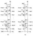
まず、選択メモリセルのデータ状態と選択メモリセルの位置に応じて読み出し電流に差が生じることを、図41〜図43を用いて具体的に説明する。図41と図42は、16個のメモリセルM0〜M15を直列接続して構成されるNANDセルユニットについて、それぞれ異なる読み出し条件を示している。NANDセルの一端は、選択トランジスタS1を介してデータ転送線(ビット線)BLに接続され、他端は選択トランジスタS2を介して基準電位となる共通ソース線SLに接続されている。各メモリセルM0〜M15の制御ゲートはそれぞれ別のデータ制御線(ワード線)WL0〜WL15に接続され、選択トランジスタS1,S2のゲートはブロック選択を行うための選択ゲート線SSL,GSLにそれぞれ接続されている。
【0005】
図41,図42では、一つのNANDセルユニットのみ示しているが、通常この様なNANDセルユニットがビット線方向、およびワード線方向に複数個配列されてメモリセルアレイが構成される。また、ビット線BLには、センスアンプ/データラッチが接続される。フラッシュメモリの場合では、ワード線方向に並んだ複数のNANDセルユニットの範囲がデータを一括消去する単位となるブロックとなる。以下では、電荷蓄積層の電子を放出したしきい値の低い状態を“1”データ(消去状態)とし、電荷蓄積層に電子を注入したしきい値の高い状態を“0”データ状態として、説明する。
【0006】
図41(a)(b)では、メモリセルM0〜M15のうちビット線BLに最も近いメモリセルM0を選択したときの読み出し電圧関係を示している。この場合、共通ソース線SLは接地電位GNDとし、ビット線BLには例えば、1V程度の正電圧VBLを与え、選択されたワード線WL0には、しきい値判定を行うための読み出し電圧Vrを、残りの非選択ワード線WL1〜WL15にはデータによらずセルをオンさせるに必要なパス電圧Vreadを与える。選択ゲート線SSL,GSLにもパス電圧Vreadを与える。
【0007】
図43は、2値データを記憶する場合のメモリセルのしきい値分布例である。“0”データのしきい値の上限Vthwとしては、例えば2V、“1”データ(消去状態)のしきい値の上限Vtheとしては−1V、またパス電圧Vreadとしては、4Vから5Vの間の電圧が用いられる。読み出し電圧Vrとしては例えば0Vが用いられる。図43には選択トランジスタS1,S2のしきい値を示したが、これらはメモリセルの書き込みしきい値上限Vthwよりも低い。従って、パス電圧Vreadを与えることにより、選択トランジスタS1,S2はコンダクタンスがメモリセルよりも大きくなり、十分導通状態を保つ。
【0008】
図41(a)は、選択メモリセルM0が“1”データであり、残りの非選択メモリセルM1〜M15も全て“1”データである場合を示しており、一方図41(b)では、選択メモリセルM0が“1”データであるが、残りの非選択メモリセルM1〜M15が全て“0”データである場合を示している。この二つのケースで、NANDセルユニットに流れる読み出し電流ID1,ID2の関係は、ID1>ID2となる。図41(b)の場合の方が図41(a)の場合よりも非選択メモリセルM1〜M15でのソース・ドレイン間の抵抗が高いためである。
【0009】
図42(a)(b)は、NANDセルの共通ソース線SLに最も近いメモリセルM15が選択された場合について、同様の読み出し電圧関係を示している。図42(a)では、全てのメモリセルM0〜M15が“1”データの場合であり、図42(b)は、選択メモリセルM15が“1”データで、残りの非選択メモリセルM0〜M14が“0”データの場合である。この場合、メモリセルM0〜M14は、VBLがVread−Vthwより小さいと活性領域(線形領域)で動作するが、図42(b)の場合の方が図42(a)の場合より直列抵抗が大きくなる。またメモリセルM15も線形領域で動作し、ドレイン・ソース間電圧は小さい。従って、図42(a),(b)の読み出し電流ID3,ID4の関係は、ID3>ID4となる。
【0010】
また、各メモリセルの基板バイアス効果を考慮すると、データ転送線BLに近いメモリセルM0には、共通ソース線SLに近いメモリセルM15より高い基板バイアスがかかり、しきい値が高くなる。従ってID2はID4より小さく、ID1はID3よりも小さくなる。
【0011】
次に、同じデータを書き込んだ場合でも、例えば、図44(a),(b)に示す消去、書き込みおよび読み出しシーケンスを経ることにより、消去状態のしきい値が上昇して観測される問題が生ずることを説明する。
【0012】
図44(a)では、まず、NANDセルユニットの全メモリセルM0〜M15が一括消去され、”1”データ状態に設定される(SE1)。その後、ステップSE2では、図41(a)の電圧関係でメモリセルM0のデータを読み出して、一定の電流レベルIthでデータが”0”か”1”かを判断する。一定電流値Ithでの判定ではなく、例えばデータ転送線をVBLにプリチャージして、浮遊状態にした後、読み出しを行って、データ転送線の電位変動をセンスアンプで検出する方法でもよい。更に、メモリセルM1からM15までに“0”データを書き込み、それらのしきい値を上昇させる(SE3)。次いで、ステップSE4で、図41(b)の電圧関係でメモリセルM0のデータを読み出し、一定の電流レベルIthでデータが”0”か”1”かを判断する。
【0013】
このようにすると、同じ消去状態のメモリセルM0でも、ステップSE2とSE4では、図41(a),(b)で説明した読み出し電流ID1,ID2の差があるから、ステップSE4では読み出し電流ID2が判定電流Ith以下となり、ステップSE2では読み出し電流ID1が判定電流Ithより大きいという事態が生じ得る。これは言い換えれば、ステップSE4の方がSE2よりも同じ電流しきい値で見た場合のしきい値分布がよりしきい値が正の方に上昇することを示しており、図43の点線と実線の状況が生じる。
【0014】
図44(b)では、まず、NANDセルユニットの全メモリセルM0〜M15が一括消去され、”1”データ状態に設定される(SE1)。その後、ステップSE2’では、図42(a)の電圧関係でメモリセルM15のデータを読み出して、一定の電流レベルIthでデータが“0”か“1”かを判断する。更に、メモリセルM0からM14までに“0”データを書き込み、それらのしきい値を上昇させる(SE3’)。次いで、ステップSE4’で、図42(b)の電圧関係でメモリセルM15のデータを読み出し、一定の電流レベルIthでデータが“0”か“1”かを判断する。
【0015】
このようにすると、同じ消去状態のメモリセルM15でも、ステップSE2’とSE4’では、図42(a),(b)で説明した読み出し電流ID3,ID4の差があるから、ステップSE4’では読み出し電流ID4が判定電流Ith以下となり、ステップSE2’では読み出し電流ID3が判定電流Ithより大きいという場合が生じる。従ってこの場合も、ステップSE4’の方がSE2’よりも同じ電流しきい値で見た場合のしきい値分布がよりしきい値が正の方に上昇し、やはり図43の点線と実線の状況が生じることになる。
【0016】
一方、同じ論理値データを読む場合に、メモリセルの読み出し電流がメモリセルの位置と、非選択メモリセルのデータによって大きく変化すると、読み出し時間の最大値を短くし、かつ、セル電流によって生ずる電磁ノイズの最大値を削減することが困難になる。これは、読み出し時間の最大値が、選択セルの読み出し電流が最も小さくなる条件で決定され、電磁ノイズの最大値は、選択セルの読み出し電流が最も大きくなる条件で決定されるからである。
【0017】
さらに、読み出しセルの電流が大きくなると、共通ソース線SLの電位の浮き上がりが大きくなり、書き込みとベリファイ読み出しを繰り返したとき、“0”データ書き込みが十分に行われなくなるという不良が生ずる(例えば、特開平11−260076号公報参照)。また、データ転送線に流れる最大電流も増大するため、電流ストレスによるエレクトロマイグレーションによる配線抵抗上昇や信頼性劣化、および、発熱増大によるトランジスタのしきい値変化やリーク電流の増大も問題となる。
【0018】
さらに、“1”データの判定しきい値が高くなると、“0”データのしきい値分布の下限と“1”データのしきい値分布の上限の差が小さくなる。この結果例えば“1”データを誤って“0”データとして読み出す誤読み出しの確率が増加する。この様な誤読み出しをなくすためには、例えば“0”データのしきい値分布をより高い方まで広げる必要が生ずる。しかしこれは、別の問題を招来する。即ち蓄積電荷の自己電界によって、高いしきい値のデータの保持特性は、低いしきい値のデータの保持特性に比べて悪いので、“0”データのしきい値分布をあまり高くすることは、十分なデータ保持特性を得ることを困難にする。またNANDセルユニットでは、非選択メモリセルにはしきい値分布の最大値よりも高い電圧を印加する必要があるため、読み出し動作を繰り返すことによって、電荷蓄積層に負の電荷が注入されてしきい値が上昇し、消去状態のしきい値の上限がより増大する。これは、データ破壊や誤読み出しの原因となる。
【0019】
【発明が解決しようとする課題】
以上述べたように、従来のNAND型EEPROMでは、データ読み出し時に、非選択メモリセルのデータ状態、および選択メモリセルのNANDセルユニット内の位置によって、読み出し電流に差があり、これが誤読み出しやデータ破壊等、EEPROMの高性能化にとって種々の問題をもたらす。
【0020】
この発明は、上記問題を解決すべくなされたもので、その目的とするところは、非選択メモリセルのデータ状態や選択メモリセルの位置による読み出し電流のばらつきを低減した半導体記憶装置を提供することにある。
【0021】
【課題を解決するための手段】
この発明に係る半導体記憶装置は、保持するデータによって電流端子間のコンダクタンスが変化し、第1の端子と第2の端子の間に複数個電流端子が直列接続された、データを電気的に再書き込み可能な複数のメモリセルと、前記第1の端子を電気的にデータ転送線に接続する第1の選択スイッチングエレメントと、前記第2の端子を基準電位線に接続する第2の選択スイッチングエレメントであるMISFETとを備えてメモリセルユニットが構成され、前記メモリセルユニットの第1及び第2の選択スイッチングエレメントを導通状態にし、選択されたメモリセルにそのデータに応じてその電流端子間を導通又は遮断状態にさせる読み出し電圧をその制御電極に印加し、前記選択されたメモリセル以外のメモリセルにそのデータによらず電流端子間を導通状態とするパス電圧をその制御電極に印加して、前記データ転送線と基準電位線との間の電流の有無又は電流の大小を検出するデータ読み出しモードを有し、前記データ読み出しモードにおいて、前記MISFETの電流端子間のコンダクタンスが、前記選択されたメモリセル以外の少なくとも一つのメモリセルについて、電流端子間のコンダクタンスを最も小さくなる状態に設定した場合のコンダクタンスより小さい状態に設定されるようにしたことを特徴とする。
【0022】
この発明に係る半導体記憶装置はまた、保持するデータによって電流端子間のコンダクタンスが変化し、第1の端子と第2の端子の間に複数個電流端子が直列接続された、データを電気的に再書き込み可能な複数のメモリセルと、前記第1の端子をデータ転送線に接続する第1の選択スイッチングエレメントであるMISFETと、前記第2の端子を電気的に基準電位線に接続する第2の選択スイッチングエレメントとを備えてメモリセルユニットが構成され、前記メモリセルユニットの第1及び第2の選択スイッチングエレメントを導通状態にし、選択されたメモリセルにそのデータに応じてその電流端子間を導通又は遮断状態にさせる読み出し電圧をその制御電極に印加し、前記選択されたメモリセル以外のメモリセルにそのデータによらず電流端子間を導通状態とするパス電圧をその制御電極に印加して、前記データ転送線と基準電位線との間の電流の有無又は電流の大小を検出するデータ読み出しモードを有し、前記データ読み出しモードにおいて、前記MISFETの電流端子間のコンダクタンスが、前記選択されたメモリセル以外の少なくとも一つのメモリセルについて、電流端子間のコンダクタンスを最も小さくなる状態に設定した場合のコンダクタンスより小さい状態に設定されるようにしたことを特徴とする。
【0023】
この発明によれば、データ読み出し時に一方の選択スイッチングエレメントのコンダクタンスを、非選択メモリセルのコンダクタンスの最小値より小さい状態に設定することによって、メモリセルユニットの非選択メモリセルのデータ状態や、選択メモリセルのメモリセルユニット内の位置によって生ずる読み出し電流のばらつき小さくすることができる。同時に、直列接続されるメモリセルの状態によるしきい値上昇量を、ほぼ0にすることができる。以上の結果、電磁ノイズ起因の誤読み出しの確率が低減され、高速読み出しが可能になる。
【0024】
この発明におけるデータ読み出しモードには具体的に、次のような態様がある。
(1)データ転送線からメモリセルユニットを介して基準電位線に読み出し電流を流すものとして、第2の選択スイッチングエレメントの制御電極の電圧を、パス電圧より低く且つ、第1の選択スイッチングエレメントの制御電極の電圧より低い第1の設定値に設定する態様。
(2)基準電位線からメモリセルユニットを介してデータ転送線に読み出し電流を流すものとして、第1の選択スイッチングエレメントの制御電極の電圧を、パス電圧より低く且つ、第2の選択スイッチングエレメントの制御電極の電圧より低い第1の設定値に設定する態様。
(3)データ転送線からメモリセルユニットを介して基準電位線に読み出し電流を流すものとして、第1の選択スイッチングエレメントの制御電極の電圧を、パス電圧より低く且つ、第2の選択スイッチングエレメントの制御電極の電圧より低い第1の設定値に設定する態様。
(4)基準電位線からメモリセルユニットを介してデータ転送線に読み出し電流を流すものとして、第2の選択スイッチングエレメントの制御電極の電圧を、パス電圧より低く且つ、第1の選択スイッチングエレメントの制御電極の電圧より低い第1の設定値に設定する態様。
【0025】
この発明において、メモリセルは例えば、半導体基板に少なくとも一つの電荷蓄積層と制御電極とを有するトランジスタ構造を有するものとする。この場合、上述したデータ読み出しモードにおけるコンダクタンスの関係は、選択スイッチングエレメント及びメモリセルを5極管動作領域で動作させる場合には、次の様に表される。即ちメモリセルのドレイン電流係数をβcell、選択スイッチングエレメントのMISFETのドレイン電流係数をβSL、メモリセルの書き込みしきい値をVthw、選択スイッチングエレメントのMISFETのしきい値をVth、パス電圧をVread、選択スイッチングエレメントのMISFETの制御電極の電圧をVGSLとして、(βSL)0.5×(VGSL−Vth)が(βcell)0.5×(Vread−Vthw)より小さくなるようにする。
また、選択スイッチングエレメント及びメモリセルを3極管動作領域で動作させる場合には、(βSL)×(VGSL−Vth)が(βcell)×(Vread−Vthw)より小さくなるようにする。
【0026】
この発明に係る半導体記憶装置はまた、保持するデータによって電流端子間のコンダクタンスが変化し、第1の端子と第2の端子の間に複数個電流端子が直列接続された、データを電気的に再書き込み可能な複数のメモリセルと、前記第1の端子を電気的にデータ転送線に接続する第1の選択スイッチングエレメントと、前記第2の端子を基準電位線に接続する第2の選択スイッチングエレメントであるMISFETとを備えてメモリセルユニットが構成され、前記メモリセルユニットの第1及び第2の選択スイッチングエレメントを導通状態にし、選択されたメモリセルにそのデータに応じてその電流端子間を導通又は遮断状態にさせる読み出し電圧をその制御電極に印加し、前記選択されたメモリセル以外のメモリセルにそのデータによらず電流端子間を導通状態とするパス電圧をその制御電極に印加して、前記データ転送線と基準電位線との間の電流の有無又は電流の大小を検出するデータ読み出しモードを有し、前記データ読み出しモードにおいて、前記第2の選択スイッチングエレメントの制御電極の電圧は、前記パス電圧より低く且つ、前記第1の選択スイッチングエレメントの制御電極の電圧より低い第1の設定値に設定されていることを特徴とする。
【0027】
この発明に係る半導体記憶装置は更に、保持するデータによって電流端子間のコンダクタンスが変化し、第1の端子と第2の端子の間に複数個電流端子が直列接続された、データを電気的に再書き込み可能な複数のメモリセルと、前記第1の端子をデータ転送線に接続する第1の選択スイッチングエレメントであるMISFETと、前記第2の端子を電気的に基準電位線に接続する第2の選択スイッチングエレメントとを備えてメモリセルユニットが構成され、前記メモリセルユニットの第1及び第2の選択スイッチングエレメントを導通状態にし、選択されたメモリセルにそのデータに応じてその電流端子間を導通又は遮断状態にさせる読み出し電圧をその制御電極に印加し、前記選択されたメモリセル以外のメモリセルにそのデータによらず電流端子間を導通状態とするパス電圧をその制御電極に印加して、前記データ転送線と基準電位線との間の電流の有無又は電流の大小を検出するデータ読み出しモードを有し、前記データ読み出しモードにおいて、前記第1の選択スイッチングエレメントの制御電極の電圧は、前記パス電圧より低く且つ、前記第2の選択スイッチングエレメントの制御電極の電圧より低い第1の設定値に設定されていることを特徴とする。
【0028】
具体的にメモリセルは、例えば半導体基板に少なくとも一つの電荷蓄積層と制御電極とを有するMISFET構造を有するものとする。この場合、データ読み出しモードにおいて、メモリセルのドレイン電流係数をβcell、選択スイッチングエレメントのMISFETのドレイン電流係数をβSL、メモリセルの書き込みしきい値をVthw、選択スイッチングエレメントのMISFETのしきい値をVth、パス電圧をVread、選択スイッチングエレメントのMISFETの制御電極の電圧をVGSLとして、(βSL)×(VGSL−Vth)が(βcell)×(Vread−Vthw)より小さくなるようにする。この様な電圧関係に設定すれば、選択スイッチングエレメントのドレイン電流係数がメモリセルのそれより大きい場合でも、選択スイッチングエレメントの一方をメモリセルよりコンダクタクスの小さい状態で動作させることが可能になる。これにより、非選択メモリセルのデータ状態や選択メモリセルの位置による読み出し電流のばらつきを小さくすることができる。
【0029】
この発明に係る半導体記憶装置は更に、保持するデータによって電流端子間のコンダクタンスが変化し、第1の端子と第2の端子の間に複数個電流端子が直列接続された、データを電気的に再書き込み可能な複数のメモリセルと、前記第1の端子を電気的にデータ転送線に接続する第1の選択スイッチングエレメントと、前記第2の端子を基準電位線に接続する第2の選択スイッチングエレメントであるMISFETとを備えてメモリセルユニットが構成され、前記メモリセルユニットの第1及び第2の選択スイッチングエレメントを導通状態にし、選択されたメモリセルにそのデータに応じてその電流端子間を導通又は遮断状態にさせる読み出し電圧をその制御電極に印加し、前記選択されたメモリセル以外のメモリセルにそのデータによらず電流端子間を導通状態とするパス電圧をその制御電極に印加して、前記データ転送線と基準電位線との間の電流の有無又は電流の大小を検出するデータ読み出しモードを有し、前記データ読み出しモードにおいて、前記メモリセルユニット内で前記基準電位線から数えて所定個数の範囲内のメモリセルが選択された場合に、前記第2の選択スイッチングエレメントの制御電極の電圧は、前記パス電圧より低く且つ、前記第1の選択スイッチングエレメントの制御電極の電圧より低い第1の設定値に設定され、前記基準電位線から数えて所定個数の範囲外のメモリセルが選択された場合に、前記第2の選択スイッチングエレメントの制御電極の電圧は、前記第1の設定値よりも高い第2の設定値に設定されるようにしたことを特徴とする。
【0030】
この発明に係る半導体記憶装置は更に、保持するデータによって電流端子間のコンダクタンスが変化し、第1の端子と第2の端子の間に複数個電流端子が直列接続された、データを電気的に再書き込み可能な複数のメモリセルと、前記第1の端子をデータ転送線に接続する第1の選択スイッチングエレメントであるMISFETと、前記第2の端子を電気的に基準電位線に接続する第2の選択スイッチングエレメントとを備えてメモリセルユニットが構成され、前記メモリセルユニットの第1及び第2の選択スイッチングエレメントを導通状態にし、選択されたメモリセルにそのデータに応じてその電流端子間を導通又は遮断状態にさせる読み出し電圧をその制御電極に印加し、前記選択されたメモリセル以外のメモリセルにそのデータによらず電流端子間を導通状態とするパス電圧をその制御電極に印加して、前記データ転送線と基準電位線との間の電流の有無又は電流の大小を検出するデータ読み出しモードを有し、前記データ読み出しモードにおいて、前記メモリセルユニット内で前記データ転送線から数えて所定個数の範囲内のメモリセルが選択された場合に、前記第1の選択スイッチングエレメントの制御電極の電圧は、前記パス電圧より低く且つ、前記第2の選択スイッチングエレメントの制御電極の電圧より低い第1の設定値に設定され、前記データ転送線から数えて所定個数の範囲外のメモリセルが選択された場合に、前記第1の選択スイッチングエレメントの制御電極の電圧は、前記第1の設定値よりも高い第2の設定値に設定されるようにしたことを特徴とする。
【0031】
この様に選択メモリセルの位置に応じて、一方の選択スイッチングエレメントの制御電極の電圧を切り換えることによって、選択メモリセルの位置に依存して生じる読み出し電流の最大値と最小値の差を小さいものとすることができる。
【0032】
この発明に係る半導体記憶装置は更に、保持するデータによって電流端子間のコンダクタンスが変化し、第1の端子と第2の端子の間に複数個電流端子が直列接続された、データを電気的に再書き込み可能な複数のメモリセルと、前記第1の端子を電気的にデータ転送線に接続する第1の選択スイッチングエレメントと、前記第2の端子を基準電位線に接続する第2の選択スイッチングエレメントとを備えてメモリセルユニットが構成され、前記メモリセルユニットの第1及び第2の選択スイッチングエレメントを導通状態にし、選択されたメモリセルにそのデータに応じてその電流端子間を導通又は遮断状態にさせる読み出し電圧をその制御電極に印加し、前記選択されたメモリセル以外のメモリセルにそのデータによらず電流端子間を導通状態とするパス電圧をその制御電極に印加して、前記データ転送線と基準電位線との間の電流の有無又は電流の大小を検出するデータ読み出しモードを有し、前記データ読み出しモードは、(1)前記データ転送線から前記メモリセルユニットを介して前記基準電位線に電流を流すものであって、前記基準電位線と前記選択されたメモリセルの間にある非選択メモリセルの制御電極に与える第1のパス電圧が、前記データ転送線と前記選択されたメモリセルの間にある非選択メモリセルの制御電極に与える第2のパス電圧よりも低く設定されるか、或いは(2)前記基準電位線から前記メモリセルユニットを介して前記データ転送線に電流を流すものであって、前記データ転送線と前記選択されたメモリセルの間にある非選択メモリセルの制御電極に与える第1のパス電圧が、前記基準電位線と前記選択されたメモリセルの間にある非選択メモリセルの制御電極に与える第2のパス電圧よりも低く設定されることを特徴とする。
【0033】
この様に、選択メモリセルよりデータ転送線側にある非選択メモリセルと基準電位線側にある非選択メモリセルに与えるパス電圧を異ならせ、読み出し電流の方向に応じてそのパス電圧の大小関係を設定することによって、非選択メモリセルでのパス電圧によるストレスを緩和することができる。また、選択メモリセルが線形動作する程度にそのしきい値が判定しきい値より大きい場合には、選択メモリセルの下流にある非選択メモリセルのコンダクタンスが低下するため、読み出し電流の最大値を抑えることができる。
【0034】
この発明に係る半導体記憶装置は更に、保持するデータによって電流端子間のコンダクタンスが変化し、第1の端子と第2の端子の間に複数個電流端子が直列接続された、データを電気的に再書き込み可能な複数のメモリセルと、前記第1の端子を電気的にデータ転送線に接続する第1の選択スイッチングエレメントと、前記第2の端子を基準電位線に接続する第2の選択スイッチングエレメントとを備えてメモリセルユニットが構成され、前記メモリセルユニットの第1及び第2の選択スイッチングエレメントを導通状態にし、選択されたメモリセルにそのデータに応じてその電流端子間を導通又は遮断状態にさせる読み出し電圧をその制御電極に印加し、前記選択されたメモリセル以外の非選択メモリセルにそのデータによらず電流端子間を導通状態とするパス電圧をその制御電極に印加して、前記データ転送線と基準電位線との間の電流の有無又は電流の大小を検出するデータ読み出しモードを有し、前記データ読み出しモードにおいて、前記選択されたメモリセルの前記メモリユニット内の位置に応じて、前記非選択メモリセルの制御電極に与えるパス電圧が切り換えられるようにしたことを特徴とする。
【0035】
具体的に、データ読み出しモードは、(1)データ転送線からメモリセルユニットを介して基準電位線に電流を流すものである場合には、選択されたメモリセルよりデータ転送線側にある非選択メモリセルの数が多くなるにつれて、パス電圧が高くなるようにし、(2)基準電位線からメモリセルユニットを介してデータ転送線に電流を流すものである場合には、選択されたメモリセルより基準電位線側にある非選択メモリセルの数が多くなるにつれて、パス電圧が高くなるようにする。
【0036】
この様に、選択メモリセルの位置に応じて、非選択メモリセルに与えるパス電圧を切り換えることによって、選択メモリセルのしきい値が論理判定しきい値より大きい場合に、非選択メモリセルでのパス電圧によるストレスを低減することができる。
【0037】
【発明の実施の形態】
以下、図面を参照して、この発明の実施の形態を説明する。
なお、以下で、トランジスタのon状態とは、トランジスタのしきい値よりも大きな電圧をゲート電極に加えて、MISFETのソース電極とドレイン電極の間が導通状態になることを示し、トランジスタのoff状態とは、トランジスタのしきい値よりも小さな電圧をゲート電極に加えて、MISFETのソース電極とドレイン電極の間が遮断状態となっていることを示す。なお、しきい値としては、ソース電極とドレイン電極とに流れる電流が、例えば、40nA×(チャネル幅W)/(ゲート長さL)となる値になったときのゲート電圧とする。また実施の形態では、通常のCMOSロジック回路の構成が簡単なため、しきい値が正であるトランジスタを例として説明し、特に言及しない場合には、例えば0.5Vから6Vの範囲のVccとなる正の電圧を制御電圧として与えた場合には、論理は“H”とし、回路がon状態となり、例えば0Vとなる電圧GNDを与えた場合には、論理は“L”とし、回路がoff状態になるとする。また、論理回路の“H”に相当する値をVccと記し、“L”に相当する値をGNDと便宜的に例として記しているが、これらはそれぞれ、電源電圧Vccに対してVcc/2以上、及びVcc/2以下の0V以上の電圧であれば、CMOS回路が動作するのでかまわない。もちろん、しきい値が負のトランジスタを用いても、ゲート電圧の可変範囲にしきい値が含まれるようにすればよいことは自明であろう。
【0038】
[実施の形態1]
図1は、実施の形態1によるNAND型EEPROMの構成を示し、図2はそのメモリセルアレイ1の構成を示している。セルアレイ1は、図2に示すように、直列接続された複数のメモリセルを含むメモリセルユニット(即ちNANDセルユニット)20をロウ方向及びカラム方向にそれぞれ複数個ずつ配列して構成される。NANDセルユニット20は、カラム方向に連続するデータ転送線(以下、ビット線という)BLとロウ方向に連続する基準電位線(以下、共通ソース線という)SLの間に接続される。メモリセルアレイ1のビット線のデータをセンスし、あるいは書き込みデータを保持するためにセンスアンプ回路4が設けられている。センスアンプ回路4はデータレジスタを兼ねており、例えばフリップフロップ回路を主体として構成される。
【0039】
センスアンプ回路4は、データ入出力バッファ7に接続されている。これらの接続は、アドレスバッファ6からのアドレス信号をデコードするカラムデコーダ5の出力によって制御され、データ入出力I/Oに与えられたデータをメモリセルアレイ1に書き込み、またメモリセルアレイ1のデータをI/Oへ読み出し可能となっている。
【0040】
メモリセルアレイ1のメモリセル選択を行うため、具体的にはデータ制御線(以下、ワード線という)WL及び選択ゲート線SSL,GSLの制御をするために、ロウデコーダ3とデータ制御線ドライバ2が設けられている。データ制御線ドライバ2は、ロウデコーダ3のデコード出力により、選択されたデータ制御線及び選択ゲート線に必要な制御電圧を与える。
【0041】
基板電位制御回路9は、セルアレイ1が形成される基板領域(通常p型ウェル)の電位を制御するために設けられている。具体的に基板電位制御回路9は、制御回路8により制御されて、データ書き込み時及びデータ読み出し時は、接地電位GNDを発生し、データ消去時に10V以上の消去電圧を発生するように構成される。
【0042】
内部電圧発生回路11は、制御回路8により制御されて、データ書き込み或いは読み出し時に、メモリセルアレイ1の選択されたメモリセルに必要な電圧を与えるための種々の内部電圧を発生するように設けられている。具体的に内部電圧発生回路11は、書き込み電圧(Vpgm)を発生するVpgm発生回路11a、書き込み時のパス電圧(Vpass)を発生するVpass発生回路11b、読み出し時のパス電圧(Vread)を発生するVread発生回路11c、読み出し時選択メモリセルに与えられる読み出し電圧(Vr)を発生するVr発生回路11d、選択トランジスタに与える制御電圧(VGSL)を発生するVGSL発生回路11eを有する。
【0043】
Vpgm発生回路11aは、データ書き込み時に選択メモリセルの制御ゲートに与えるための、電源電圧よりも昇圧された書き込み電圧Vpgmを発生する。Vpass発生回路11bは、データ書き込み時に非選択メモリセルの制御ゲートに与えるための、書き込み電圧Vpgmより低く、電源電圧より高いパス電圧Vpassを発生する。Vread発生回路11cは、データ読み出し時に非選択メモリセルの制御ゲートに与えるための、電源電圧より高いパス電圧Vreadを発生する。Vr発生回路11dは、データ読み出し時に選択メモリセルの制御ゲートに与えるしきい値判定のための読み出し電圧Vrを発生する。
【0044】
VGSL発生回路11eは、この発明において特徴的なものであり、データ読み出し時に選択トランジスタのゲートに与えるための、選択電圧VGSLを発生する。この電圧VGSLは、非選択メモリセルに与えられるパスVreadよりも低く設定される。特に、電圧VGSLを電源電圧Vcc以下にすれば、VGSL発生回路11eとして昇圧回路を必要とせず、回路面積を削減することができ、また選択トランジスタの電界ストレスを低減し、信頼性を向上することができる。
【0045】
このVGSL発生回路11eは、チップ形成後プログラム可能な電源回路として構成することが好ましい。これは、チップ間のしきい値ばらつきが存在しても、電圧VGSLをチップ毎に補正することができるためである。例えば、VGSL発生回路11eに、幾つかの電圧値に対応するヒューズ回路や不揮発性メモリ素子を内蔵し、出荷時にチップ毎のしきい値上昇量を測定し、そのデータを用いてヒューズ切断または不揮発性メモリ素子にプログラムする。これにより、ウェハダイシングを行った後でも、電圧VGSLを補正をすることができる。或いはまた、電圧VGSLを内部電源回路ではなく、外部から供給するように構成することも、チップのばらつきに対応するためには有効である。
【0046】
具体的に、書き込み電圧Vpgmは、6V以上30V以下の電圧である。書き込み時のパス電圧Vpassは、3V以上15V以下の電圧である。読み出し時のパス電圧Vreadは、1V以上9V以下の電圧である。このパス電圧Vreadは、書き込みしきい値の上限よりも1Vから3V程度高い値に設定することが、読み出し電流を十分確保し且つ、データ破壊等を防止する上で望ましい。読み出しVrは、“0”,“1”データのしきい値分布の分離幅の中間に設定する。
【0047】
ソース電圧制御回路10は、制御回路8の制御によって、メモリセルアレイ1の基準電位線である共通ソース線の電圧を書き込み、消去および読み出しに応じて制御する。図1では省略しているが、制御回路8により、センスアンプ4の活性化を制御する制御信号やビット線選択信号sel1、sel2等が出力される。
【0048】
図2に示すメモリセルアレイ1では、ワード線WL0〜WL15、及び選択ゲート線(ブロック選択線)SSL、GSLは省略しているが、破線で示すロウ方向に並ぶ全NANDセルユニット20(この範囲がデータの一括消去の範囲となるブロックとなる)で共有されている。また図2では、カラム方向(ビット線方向)、およびロウ方向(ワード線方向)にそれぞれ3つ、2×512ずつのNANDセルユニット20が配置された構造を示したが、これは一般に複数個であればよく、アドレスデコードの関係で好ましくは、2i個(iは正の整数)とする。
【0049】
カラム方向に複数のNANDセルユニット20で共有されるビット線BLxa、BLxb(x=1,2,…,512)は、図3に示すようにトランジスタQxaおよびQxbを介して、センスアンプ回路4の1つのセンスアンプSAxに接続されている。センスアンプ回路4においては、メモリセル1つよりも大きなトランジスタを必要とするため、1つのセンスアンプSAxを複数のビット線で共有し、センスアンプの占める面積を縮小している。図3では、一つのセンスアンプに接続されるビット線BLはそれぞれ2本の場合を示したが、例えば1本や4本でもよく、2n本(nは自然数)であることがアドレスデコード回路が簡略化でき望ましい。
【0050】
センスアンプ回路4は、前述のようにメモリセルのデータを読み出す働きと共に、メモリセルへの書き込みデータを一時保持するデータレジスタを兼ねている。さらに、センスアンプ回路4は、トランジスタQaxa,Qaxbを介して、データ入出力バッファ7に接続されるデータ線I/OおよびI/OBと接続されている。データ線I/OおよびI/OBは、その電圧変動によるビット線BLへの容量結合ノイズを減らすためには、セルの列方向に形成されることが望ましい。トランジスタQaxaおよびQaxbのゲートは、カラムデコーダ5の出力により制御され、これにより、データ線I/OまたはI/OBに与えられたデータをセンスアンプ回路4に読み込み、またセンスアンプ回路4からデータ線I/OまたはI/OBにデータを出力できるようになっている。
【0051】
図2において、共通ソース線SLは、セルアレイ1のロウ方向に、複数のNANDセルユニット20に共通に配設されている。更にこの共通ソース線SLをカラム方向に短絡する配線SLyが設けられて、共通ソース線SLと共に網目構造をなしている。これにより、共通ソース線SLの読み出し電流による電位上昇を抑えている。配線SLyは、メモリセルアレイ1の半導体基板上の拡散領域やデータ転送線と同層の配線層で形成されているため、その領域にはメモリセルを配置することはできない。よって、ビット線BLの線密度を配線SLyの線密度よりも大きくすることにより、セルの占有面積を確保するようにしている。
【0052】
図2の例では、512本のビット線BL毎に1つの短絡用配線SLyがされているが、配線SLyの1本あたりのビット線の本数は複数であれば構わない。この共通ソース線SLは、ソース線電圧制御回路10に電気的に接続されている。このソース線電圧制御回路10は、データ読み出し時には接地電位GNDを出力する回路である。
【0053】
センスアンプ回路4は、制御回路40から与えられる活性化信号により同時に活性化され、複数のビット線のデータを同時に読み出すことが可能となっている。トランジスタQxaのゲートは、ロウ方向に共通に制御線sel1に接続され、トランジスタQxbのゲートも同様にロウ向に共通に制御線sel2に接続されている。これにより、稠密に配置されたメモリセルアレイ1の選択を選択信号sel1およびsel2を用いて小さな配線面積で行うことができる。
【0054】
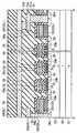
図4(a),(b)は、それぞれ、一つのNANDセルユニット20の等価回路と3つのNANDセルユニット分の平面図を示している。NANDセルユニット20は、電荷蓄積層である浮遊ゲート26を有するMISFET構造の不揮発性メモリセルM0〜M15が直列に接続され、その一端がMISFETからなる選択トランジスタS1を介してビット線にBLに接続され、他端がMISFETからなる選択トランジスタS2を介して共通ソース線SLに接続されている。メモリセルM0〜M15の制御ゲートは、ワード線28(WL0〜WL15)に接続されている。ビット線BLに沿った複数のNANDセルユニットから1つのNANDセルユニットを選択してビット線BLに接続するため、選択トランジスタS1,S2のゲート電極はそれぞれ選択ゲート線28(SSL),28(GSL)(ブロック選択線)SSL,GSLに接続されている。
【0055】
選択トランジスタS1,S2のゲートが接続される選択ゲート線SSLおよびGSLは、メモリセルの制御ゲートが接続されるワード線WL0〜WL15の浮遊ゲート26と同じ層の導電体によって、メモリセルアレイのロウ方向に連続的に形成される。なお、NANDセルユニット20には、選択ゲート線SSLおよびGSLは少なくとも1本以上あればよい。この実施の形態では、NANDセルユニット20として16=24個のメモリセルが接続されている例を示したが、ビット線およびワード線に接続されるメモリセルの数は複数であればよく、2n個(nは正の整数)であることがアドレスデコードをする上で望ましい。
【0056】
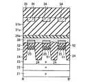
図5及び図6は、図4(b)のA−A’,B−B’,C−C’断面を示している。セルアレイは、p型シリコン基板21のn型ウェル22に形成されたp型ウェル23内に形成されている。p型ウェル23は例えば、ボロン濃度が1014cm-3から1019cm-3の間に設定されている。p型ウェル23は、n型ウェル22によってp型シリコン基板21とは分離されて、独立に電圧印加できるようになっており、これが消去時の昇圧回路負荷を減らし消費電力を抑える。
【0057】
p型ウェル23の表面に、3nmから15nmの厚さのシリコン酸化膜またはオキシナイトライド膜からなるゲート絶縁膜25を介して、例えばリンまたは砒素を濃度1018cm-3から1021cm-3の範囲で添加したポリシリコンにより、各メモリセルの浮遊ゲート26及びこれと同時に形成された選択トランジスタS1,S2のゲート電極26(SSL),26(GSL)が10nmから500nmの厚さで形成されている。ゲート絶縁膜25は、メモリセルM0〜M15と選択トランジスタS1,S2とが同じ膜厚のものを用いている。
【0058】
浮遊ゲート26は、シリコン酸化膜からなる素子分離絶縁膜24により区画された素子形成領域に形成されている。これは例えば、p型ウェル23上に全面的にゲート絶縁膜25を介して浮遊ゲート26の材料膜を堆積した後、これをパターニングし、更にp型ウェル23を例えば0.05〜0.5umの深さエッチングし、素子分離絶縁膜24を埋め込むことで形成することができる。これにより浮遊ゲート26を段差のない平面に全面形成できる。
但し浮遊ゲート26と同じ材料を用いて形成されるゲート電極26(SSL),26(GSL)は、セルアレイ1のロウ方向に連続的に形成されて、これらが選択ゲート線SSL,GSLとなる。
【0059】
浮遊ゲート26上には厚さ5nmから30nmの間のシリコン酸化膜またはオキシナイトライド膜、またはシリコン酸化膜/シリコン窒化膜/シリコン酸化膜からなるブロック絶縁膜27を介して、例えばリン、砒素、またはボロンを1017〜1021cm-3の濃度で添加したポリシリコン、または、WSi(タングステンシリサイド)とポリシリコンとのスタック構造、または、NiSi,MoSi,TiSi,CoSiとポリシリコンのスタック構造からなる制御ゲート28,28(SSL),28(GSL)が10nmから500nmの厚さで形成されている。この制御ゲート28は、セルアレイのロウ方向に連続的に形成されて、ワード線WL0〜WL15となる。また制御ゲート28(SSL),28(GSL)は同様にロウ方向に連続的に形成されて、ゲート電極26(SSL),26(GSL)と短絡されて、選択ゲート線SSL,GSLを構成する。
【0060】
この実施の形態のゲート形状では、p型ウェル23の素子形成領域の側壁が絶縁膜24で覆われているので、浮遊ゲート26を形成する前のエッチングでp型ウェル23が露出することがなく、浮遊ゲート26がp型ウェル23よりも下に来ることを防ぐことができる。よって、p型ウェル23と絶縁膜24との境界での、ゲート電界集中やしきい値低下した寄生トランジスタが生じにくい。さらに、電界集中に起因する書込みしきい値の低下現象が生じにくくなるため、より信頼性の高いトランジスタを形成することができる。
【0061】
図5に示すように、ゲート構造の上面はシリコン窒化膜29aで覆われ、両側面も例えば5nmから200nmの厚さのシリコン窒化膜(またはシリコン酸化膜)からなる側壁絶縁膜29bが形成される。そしてゲート電極に自己整合的にソース,ドレインとなるn型拡散層30が形成されている。これら拡散層30、浮遊ゲート26、および制御ゲート28により、浮遊ゲート26に蓄積された電荷量を情報量とする浮遊ゲート型EEPROMセルが形成されており、そのゲート長としては、0.5um以下0.01um以上とする。ソース,ドレインのn型拡散層30としては、例えばリンや砒素、アンチモンを表面濃度が1017cm-3から1021cm-3となるように深さ10nmから500nmの間で形成されている。さらに、これらn型拡散層30は隣接するメモリセル同士共有され、NANDセルユニットが実現されている。
【0062】
この実施の形態において、選択トランジスタS1,S2のゲート電極26(SSL),26(GSL)のゲート長(チャネル長)は、メモリセルのゲート長よりも長く、例えば、1um以下0.02um以上として形成している。これによりブロック選択時と非選択時のオンオフ比を大きく確保でき、誤書き込みや誤読み出しを防止できる。また、これら選択トランジスタS1,S2は、メモリセルと同じゲート絶縁膜25を有することが工程を削減しコストを低下させるのに望ましい。
【0063】
NANDセルユニットの両端部のn型拡散層30d,30sのうち、n型拡散層30dは、層間絶縁膜31aに埋め込まれたコンタクトプラグ32を介して中継電極33aに接続され、これが更に層間絶縁膜31bを介してビット線34に接続される。ビット線34は、タングステンやタングステンシリサイド、チタン、チタンナイトライド、アルミニウム等により形成され、セルアレイのカラム方向に連続的に配設される。もう一方のn型拡散層30sはコンタクトプラグ32を介して、中継電極33aと同時に形成された、セルアレイのロウ方向に連続する共通ソース線33bに接続されている。共通ソース線33bには、ビット線34と同じ材料を用いることができる。コンタクトプラグ32には、不純物がドープされた多結晶シリコン、タングステン、タングステンシリサイド、アルミニウム、アルミニウム、チタン、チタンナイトライド等が用いられる。
【0064】
但し、n型拡散層30sをセルアレイ1のロウ方向に連続的に形成して、これを共通ソース線SLとすることもできる。ビット線BLの上はSiO2、SiN、ポリイミド等の絶縁膜保護層35で覆われる。また、図には示していないが、ビット線BL上に、W,AlやCuからなる上部配線が形成されている。
【0065】
この様に構成されたNAND型EEPROMにおいて、この発明はデータ読み出し法に特徴を有し、これについては後に詳細に説明する。データ消去及び書き込みについては従来と同様に、例えば特開2000−76882に開示されている方法で行われる。簡単に説明すれば、データ消去は、図2に破線で示す、ワード線を共有するNANDセルブロック単位で一括消去が行われる。このとき、基板電位制御回路9から発生される昇圧された消去電圧Veraがメモリセルアレイのp型ウェルに与えられ、選択されたNANDセルブックの全ワード線を0Vとする。これにより、そのNANDセルブロック内で全メモリセルの浮遊ゲートの電子がトンネル電流により基板に放出され、しきい値の低いオール“1”状態(消去状態)になる。
【0066】
データ書き込みは、ビット線BLに書き込むべきデータに応じて例えば、Vcc(“1”データの場合、即ち書き込み禁止の場合)、Vss(“0”データの場合)を与え、これによりNANDセルチャネルをプリチャージする。高レベルにプリチャージされたNANDセルチャネルは、ビット線側選択トランジスタS1がオフになることで、フローティングになる。その後、選択されたワード線に昇圧された書き込み電圧Vpgmを与え、非選択ワード線にはパス電圧Vpassを与える。
【0067】
これにより、選択ワード線と低レベルに設定されたチャネルとの間には高電界がかかって浮遊ゲートに電子が注入されて、しきい値の高い“0”データが書かれる。フローティングの高レベルにプリチャージされたチャネルは、容量カップリングにより電位上昇して電子注入が生ぜず、“1”データ状態(消去状態)を維持する。パス電圧が与えられた非選択ワード線に沿うメモリセルでも、電子注入は生ぜず、“1”データを保持する。
【0068】
データ消去及び書き込み時には通常、消去及び書き込みを確認するためのベリファイ読み出しが行われる。即ち消去パルス印加と消去ベリファイ読み出しとを繰り返して、一定の消去しきい値範囲に追い込む。データ書き込みの場合にも、書き込みパルス印加と書き込みベリファイ読み出しとを繰り返すことにより、一定の書き込みしきい値範囲に追い込む。
【0069】
この実施の形態でのデータ読み出し動作を次に具体的に説明する。
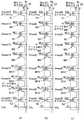
図7は、ワード線WL0を選択して、読み出し電流がビット線BLから共通ソース線SL側に流れるようにした場合のデータ読み出しタイミング図を示す。図8は、図7におけるビット線ディスチャージ期間及び引き続くセンス期間の間、選択された一つのNANDセル20に着目して、これに印加される電圧関係を示している。
【0070】
ここでは、NANDセル内のビット線BLに最も近いメモリセルM0が選択された場合を示しているが、図7及び図8では、括弧内にメモリセルM0の代わりに共通ソース線SL側のメモリセルM15が選択された場合を示している。
【0071】
データ読み出し時、データを読み出すブロックに対応するロウデコーダ3およびデータ制御線ドライバ2が活性化され、選択ゲート線SSLにパス電圧Vread、ワード線WL0に読み出しVr、残りの非選択ワード線WL1〜WL15にパス電圧Vread、選択ゲート線GSLには接地電位GNDが印加される(時刻t0)。なお、非選択のブロックの選択ゲート線SSL,GSL及びワード線WL0〜WL15は、読み出し期間中フローティング又は0Vに維持され、データの誤読み出しや破壊が生じないようにする。
【0072】
読み出し電圧Vrは、図9に示す、“0”データ書き込み後のしきい値分布の下限値をVthw2、データ消去後の“1”データのしきい値分布の上限値をVtheとして、Vthw2とVtheとの範囲内となる値である。読み出しマージンを考慮すると、Vr=(Vthw2+Vthe)/2程度とすることが、最も望ましく、例えば−0.5Vから4Vの間に設定される。特に、Vtheが負で、Vthw2が正となるように設定すれば、読み出し電圧Vrを接地電位GNDに設定でき、この場合にはVr発生回路11dが不要となるので望ましい。
【0073】
また読み出し電圧Vrとしては、接地電位GND以上の電圧となるように設定することが望ましい。これにより、データ制御線ドライバ2のワード線WL0〜WL15に接続されたトランジスタの拡散層に負電圧を印加されることが無くなり、負電圧発生回路が不要となる。よって、データ制御線ドライバ2のnチャネルMISFETが形成されたp型ウェルを接地電位GNDとして、p型基板21とn型領域で分離することなく形成することができる。これにより、データ制御線ドライバ2の回路面積を減少させることができる。さらに、負電圧が印加されないので、拡散層が順バイアスされることによる少数キャリア注入がなくなり、ラッチアップを防ぐことが可能になる。更にワード線WL0〜WL15とメモリセルアレイ1内で短絡不良が生じても、メモリセルアレイ1のp型ウェル23やn型拡散層30に負電圧が印加されることがないので、少数キャリア注入による読み出しデータ破壊が生じることもない。
【0074】
非選択ワード線WL1〜WL15及び選択ゲート線SSLに与えられるパス電圧Vreadは、Vread発生回路11cから出力され、メモリセルの“0”データのしきい値分布の上限値Vthwよりも高い電圧に設定される。
【0075】
この実施の形態では、図5に示したように、選択トランジスタS1,S2のゲート長(チャネル長)は、メモリセルM0〜M15の制御ゲートのゲート長よりも大きくなっている。一方、これらのゲート材料であるCoSiやTiSiでは、線幅が小さくなると抵抗が上昇する細線効果が存在することが知られている。よって、選択トランジスタS1,S2のゲート電極の方がメモリセルM0〜M15の制御ゲートよりも低抵抗となり、選択トランジスタS1のゲートの方がメモリセルM0〜M15の制御ゲートより高速にパス電圧Vreadまで昇圧される。また、ワード線WL0〜WL15よりも抵抗の小さい選択ゲート線GSLをビット線ディスチャージ期間に駆動することによって、並列に接続されたメモリセルの読み出しタイミングのばらつきを低減することができる。
【0076】
以上のワード線WL0〜WL15、選択ゲート線SSLの立ち上げに少し遅れて、ビット線BLをセンスアンプ回路4に内蔵された電源ノードを用いてVBLに充電する(時刻t1)。ここでVBLとしては、接地電位GND以上電源電位Vcc以下となることがセンスアンプ回路4を構成するトランジスタの信頼性をVcc程度で保証すればよいので望ましい。
【0077】
また、VBLは、センスアンプトランジスタとしてnチャネルMISFETを用いた場合には、そのしきい値以上とすることがセンスアンプ感度を向上させるのに望ましく、例えば1V程度とする。このようにすることにより、メモリセルM0が“1”、すなわち消去状態の場合には、選択トランジスタS1からメモリセルM0〜M15までのソース、ドレイン及びチャネル領域をVBLに充電する。即ちここまでは、ビット線BLおよびNANDセルユニットを充電する、ビット線(BL)プリチャージ期間である。
【0078】
このBLプリチャージ期間は、非選択ワード線が十分にパス電圧Vreadに昇圧するまでの時間以上必要であり、例えば100nSから10uSの間の時間とする。ついで、共通ソース線SL側の選択ゲート線GSLを、正の制御電圧VGSLにする(時刻t2)。制御電圧VGSLは、図9に示すように、選択トランジスタS1,S2のしきい値電圧上限Vth以上で、パス電圧Vread以下の電圧とする。これにより、メモリセルM0のしきい値がVr以下ならば、NANDセルユニットが導通状態となり、ビット線BLの電位は低下する。
【0079】
メモリセルM0のしきい値が読み出し電圧Vrより高いならば、即ち“0”データならば、メモリセルM0はオフとなり、ビット線BLの電位低下はない。つまりビット線BLは、メモリセルM0のデータ状態に応じて放電され、これがビット線(BL)ディスチャージ期間になる。このBLディスチャージ期間は、ビット線BLが十分放電するまでの時間以上必要であり、例えば100nSから100uSの間の時間とする。
【0080】
ついで、ビット線BLの電位変化を、センスアンプ回路4で判定し、データをデータラッチ内に読み出す(時刻t3)。この際、センスアンプ回路4内にビット線に対する電圧クランプ回路を備えれば、BL電位を大幅に変化させなくてもデータを高感度で読み出すことができる。センスアンプ回路は電流センス型でもよい。
【0081】
センス期間が終了した後、時刻t4で選択ゲート線GSL,SSL、ワード線WL0〜WL15、及びビット線BLの電位を初期値に戻すための、リカバリ期間に入る。
【0082】
この実施の形態では、従来例と異なり、共通ソース線SL側の選択トランジスタS2のゲートを駆動する制御電圧を、非選択ワード線に与えるパス電圧Vreadより低い電圧VGSLを用いている点がポイントである。これにより、選択トランジスタS2のコンダクタンスは、選択メモリセルM0以外の非選択メモリセルM1〜M15内の最も高いしきい値を有するメモリセルのコンダクタンスより小さくなる。
【0083】
以下にこの点を詳細に説明する。
図9は、この実施の形態でのしきい値関係を示したものである。この実施の形態では、前述したコンダクタンスの大小関係を実現するために、選択ゲート線GSLの電圧VGSLと、選択トランジスタS2のしきい値の上限(=Vth)との差ΔV2を、パス電圧Vreadとメモリセルの書き込みしきい値分布の上限Vthwとの差ΔV1よりも小さくする。
【0084】
図10は、そのゲート電圧条件において、ソースを接地した場合のメモリセルと選択トランジスタS2とのドレイン電流IDとドレイン電圧VDの特性の典型特性を示す。太い実線がメモリセルの特性を示すが、メモリセルにおいては、Vread−Vthw以上にドレイン電圧VDが上昇したところでピンチオフ領域(5極管動作領域、即ちドレイン電流が飽和する飽和領域)となる。一方、細い実線は選択トランジスタS2の特性を示すが、選択トランジスタS2においては、VGSL−Vth以上にドレイン電圧が上昇したところで飽和領域となり、それ以下のドレイン電圧では、3極管動作領域即ち線形領域となる。
【0085】
図10の破線で示しているのは、ゲートにVreadが与えられている従来例の選択トランジスタS2のドレイン電流とドレイン電圧の特性である。従来例では、0以上の任意の電流値で観測した場合のドレイン電圧は、読み出しメモリセル以外のメモリセルの方が選択トランジスタよりも大きい。これは、図43で説明したように、Vthw>Vthであること、および、選択トランジスタS2のドレイン電流係数をβSLとし、メモリセルのドレイン電流定数βcellとすると、βSL>βcellであることによる。
【0086】
ここで、ドレイン電流係数βは導電係数とも呼ばれ、MISFETのゲート長をL、チャネル幅をW、チャネル中のキャリアの平均移動度をμとし、制御ゲートから見たチャネルに対する単位面積当たりのゲート容量をCgateとした場合に、周知のように、β=(W×μ)/(Cgate×L)となる。メモリセルにおいては、制御ゲートと浮遊ゲート間容量の全容量に対する比、すなわち、カップリング比をγcr,浮遊ゲートと制御ゲート間の単位面積あたりの容量をCoxとすると、メモリセルにおける制御ゲートから見たチャネルに対する単位面積当たりのゲート容量Cgateはほぼ、Cox/γcrとなると考えればよい。
【0087】
一方、この実施の形態の構成では、選択トランジスタS2におけるゲート電極は浮遊ゲートと短絡されており、そのゲート電極から見たチャネルに対する単位面積当たりのゲート容量はCoxとなる。一般に、NANDフラッシュメモリでは、図4(b)で示すように、チャネル幅Wはメモリセルと選択トランジスタで等しく、Lgateをメモリセルのゲート長、LSLを選択トランジスタS2のゲート長として、LSL<Lgate/γcrが成立し、チャネル中のキャリアの平均移動度μは、同一のゲート絶縁膜電界ではほぼ等しいので、選択トランジスタS2とメモリセルのドレイン電流係数の関係は、下記数1となる。この実施の形態の場合、選択トランジスタS1とメモリセルの関係も同様である。
【0088】
【数1】
βSL>βcell
【0089】
一方、図10に細い実線で示す選択トランジスタS2について、ある電流値I0で観測した場合のドレイン電圧Vaは、太い実線で示すメモリセルの場合の電圧Vbより高い。言い換えれば、I0の電流を流した場合のコンダクタンスは、選択トランジスタS2の方がI0/Vaであり、メモリセルのI0/Vbよりも小さくなる。よって、メモリセルM15と選択トランジスタS2との直列接続部分を考えると、従来例では、メモリセルM15のドレインと選択トランジスタS2のソースとの間の電流は、メモリセルM15によって制限されるのに対して、この実施の形態の条件では、選択トランジスタS2によって制限される。つまりこの実施の形態では、メモリセルM15のしきい値状態によらず、選択トランジスタS2によってNANDセルの読み出し電流が支配的に制限され、均一なセル電流をメモリセルに流すことができる。
【0090】
ここで、線形領域に関しては、選択トランジスタS2のコンダクタンスID/VDは、βSL×(VGSL−Vth−VD/2)に比例し、飽和領域においては、(βSL/2)×(VGSL−Vth)2/VDに比例する。よって、選択トランジスタS2のドレイン電圧VDが上昇するほど、コンダクタンスが小さくなる。つまり、読み出し電流が増加すると、より選択トランジスタS2による電圧低下量が増大し、従来例よりもデータを読み出すセルの電流端子間の電圧が減少する負帰還がかかる。
【0091】
さらに、この効果は、単にコンダクタンスが一定である抵抗成分がメモリセルに直列に接続されているよりも大きい。よって、読み出しメモリセル以外の非選択メモリセルのデータや、読み出しセルの位置によって生ずる読み出し電流のばらつきを従来例よりも小さく抑えることができ、しきい値の上昇量の最大値を抑えることができる。
【0092】
飽和領域について選択トランジスタS2のコンダクタンスが、メモリセルのコンダクタンスよりも小さくなれば、選択トランジスタS2を飽和領域で用いることによりこの実施の形態の効果を得ることができる。その条件は、先の数1に拘わらず、下記数2を満たせばよいことになる。
【0093】
【数2】
(βSL)0.5×(VGSL−Vth)<(βcell)0.5×(Vread−Vthw)
【0094】
また、線形領域を用いた場合にも、選択トランジスタS2のコンダクタンスがメモリセルのそれより小さくなるためには、下記数3の条件を満たせばよい。
【0095】
【数3】
(βSL)×(VGSL−Vth)<(βcell)×(Vread−Vthw)
【0096】
即ち、数2及び数3の条件を満たせば、読み出し時にどの様なトランジスタ動作領域で動作させた場合にも、この実施の形態の効果が得られる。
数1に示したようにこの実施の形態の場合、βSL>βcell としているが、にも拘わらず数2又は数3を成立させるためには、下記数4の条件を満たすことがこの実施の形態の効果を得る上で必要となる。
【0097】
【数4】
(VGSL−Vth)<(Vread−Vthw)
【0098】
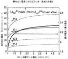
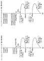
図11は、VBL=1V、Vread=5V、Vr=GND、Vthw=2V、Vthe=−1V、VSSL=5Vとし、選択トランジスタS1とS2のソース接地時で基板バイアスが0Vの場合のしきい値を0.5Vとし、βSL=2.5βcellとした場合の、電圧VGSLに対する、図41及び図42で説明した4つの読み出し状態の読み出し電流ID1〜ID4を示したものである。但し、基板バイアス効果定数を0.5[V0.5]、ドレイン電圧に対するしきい値低下量(Drain Induced Barrier Lowering定数)を0.49[V/V]としている。
【0099】
図11の右軸は、ID1〜ID4の間での、最大電流/最小電流の比を示している。従来例は、図11のVGSL=5Vの場合に相当する。電圧VGSLをVreadより低下させることにより、最大電流/最小電流の比は小さくなり上述の効果があることが判る。さらに、図中に矢印で、この実施の形態の効果が生じる電圧VGSLに対する(βSL)0.5×(VGSL−Vth)<(βcell)0.5×(Vread−Vthw)の条件を示している。
【0100】
最大電流/最小電流比が減少する効果は、ほぼ、(βSL)0.5×(VGSL−Vth)<(βcell)0.5×(Vread−Vthw)が成立する条件、すなわち、VGSL<2.4[V]で大きく増加しており、この条件で臨界的な振る舞いをすることが判る。また、従来、フラッシュNANDメモリの電源電圧Vccは2.5V以上なので、VGSLを電源電圧以下の設定にすることにより、最大電流/最小電流の比は小さくなり上述の効果が大きくなることが判る。
【0101】
図12は、図44(a)のシーケンスによるメモリセルM0の消去しきい値上昇を実線で、図44(b)のシーケンスによるメモリセルM15の消去しきい値上昇を点線で示す。これら電圧関係は、図11と同じものを用いている。電圧VGSLをパス電圧Vreadより低下させることにより、メモリセルM0およびM15のしきい値上昇量とも減少していることが明らかである。最大電流/最小電流の比を小さくする効果としきい値上昇量を小さくできる効果が両立することがわかる。
【0102】
図11の電流変化は、読み出しメモリセル以外の非選択メモリセルのデータパターンとして、最も電流値が大きなパターンと最も電流値が小さなパターンを選んでおり、他の任意のデータパターンではこの電流の最大値と最小値の間になることは明らかである。さらに、最もビット線BLに近いメモリセルM0と、最も共通ソース線SLに近いメモリセルM15の場合のみ示したが、その他のメモリセルM1〜M14についても、図11の電流の最大値と最小値の間になることも明らかであろう。言い換えれば、図11は、ランダムな順番でワード線WL0〜WL15に書き込み/読み出しした場合の最悪の読み出し電流変化量を示している。
【0103】
比較のために、電圧VGSLをパス電圧Vreadとし、読み出し電圧Vrのみを変化させることによって最大電流/最小電流の比を調整した従来例を、図13及び図14に示す。これらは図11および図12にそれぞれ対応し、VGSLとVr以外の条件は同じである。従来例では、図13のように、読み出し電圧Vrのみを上昇させると、最大電流/最小電流の比は小さくなるが、Vrに対して単調に変化し、臨界的に変化する特性は示さない。
【0104】
また、図14のように、Vrのみを上昇させると、メモリセルM0のしきい値上昇量は増加量してしまうため、メモリセルM0およびM15のしきい値上昇量を減少させることと、最大電流/最小電流比を小さくすることとは、すべて満たすことはできない。また、図13のように、読み出し電圧Vrのみを上昇させると、ID1〜ID4のなかで最大電流となるID3が上昇するため、セル電流によって生ずる電磁ノイズの最大値を削減することが困難になる。
【0105】
さらに、読み出しセルの電流が大きくなると、例えば、特開平11−260076で指摘されているように、共通ソース線SLの電位の浮き上がりが大きくなり、ベリファイ書き込み時に”1”データが”0”データに十分書き込まれない不良が生ずる。勿論、データ転送線に流れる最大電流も増大するため、電流ストレスによるエレクトロマイグレーションによる配線抵抗上昇や信頼性劣化、および、発熱増大によるトランジスタのしきい値変化やリーク電流の増大が問題となる。
【0106】
これに対してこの実施の形態では、電圧VGSLを低下させると、図11のように、ID1〜ID4のなかで最大の電流となるID3を減少させることができる。これにより、読み出し時間の最大値を一定としたままで、セル読み出し電流によって生ずる電磁ノイズの最大値を削減することができる。よって、より小さなセル電流を用いても電磁ノイズ、例えば、隣接するデータ転送線間の容量結合による電位変化の影響を受けることなく読み出しを行うことができ、高速でデータ判定をすることができ、電磁ノイズ起因の誤読み出しの確率を減少させ高信頼性を得ることができる。
【0107】
また、読み出しセルの最大電流を小さく保つことができるので、共通ソース線SLの電位の浮き上がりが小さくなり、ベリファイ書き込み時に”1”データが”0”データに十分書き込まれない不良が生じにくくなる。また、データ転送線に流れる最大電流も増大するため、電流ストレスによるエレクトロマイグレーションによる配線抵抗上昇が生じず、信頼性劣化も抑えられる。さらに、発熱増大によるトランジスタのしきい値変化やリーク電流の増大の問題も小さくすることができる。
【0108】
本発明者等は、特に、図12に黒丸で示すように、メモリセルM15を読み出す場合において、例えば電圧VGSLを低下させることにより、読み出し電圧VrをGNDに保ったままでしきい値の上昇を0とすることができることを発見した。従来例ではしきい値の上昇を0とするには、図14から明らかなように、0.3Vより遥かに高い読み出し電圧Vrでしか実現できず、ゲート判定しきい値が上昇する弊害があり、“0”データと判定しきい値との分離が困難となる。この実施の形態では、メモリセルに対する読み出し電圧VrはGNDのままなので、メモリセルの“0”データとの分離が困難となる事態は発生せず、しきい値分布を、VGSLをVreadとした場合と同じ状態に設定したままで、安定してデータ検出することができる。
【0109】
さらに、本発明者等は、メモリセル例えば、M15のしきい値上昇の成分を詳細検討の上分析し、基板バイアス効果によって読み出し電流が減少した場合、しきい値を低下させる効果があることを発見した。例えば従来例では、図42(a)から同図(b)の状態に遷移して読み出し電流が低下すると、選択トランジスタS2のコンダクタンスが、読み出しメモリセル以外の非選択メモリセルのコンダクタンスより大きいので、メモリセルM15のソース電位はほとんど変化しない。従って従来例で説明したように、ある一定の電流レベルIthでのメモリセルM15のしきい値が増大する。
【0110】
一方、本実施の形態では、選択トランジスタS2のコンダクタンスが、読み出しメモリセル以外の非選択メモリセルのコンダクタンスより小さいので、読み出し電流が低下すると、読み出しメモリセルM15のソース電位は大きく低下する。これにより、読み出し電流が減少すると、(ソース電位の減少分)+(基板バイアス効果の減少分)だけ、メモリセルM15のゲートから測定したしきい値は低下する。よって、図7,8において、選択ゲート線SSLの電圧が(VGSL+VBL)より高ければ、ビット線側の選択トランジスタS1のコンダクタンスが共通ソース線側の選択トランジスタS2のコンダクタンスより大きくなり、本実施の形態の効果が得られる。従って選択トランジスタS1のゲートをパス電圧Vreadまで昇圧する必要は必ずしも生じないことが、この解析結果から判明した。
【0111】
以上に説明した実施の形態の効果を列記すれば、次のようになる。
(a)選択トランジスタのゲート制御電圧を低くすることにより、選択メモリセルに直列接続された非選択メモリセルのデータ、および選択メモリセルの位置によって生ずる読み出し電流の変動を小さくでき、同時に、非選択メモリセルのデータ状態によるしきい値上昇量を抑えることができる。
【0112】
(b)読み出し電流の変動を小さくできることから、読み出し時間の最大値と最小値との差を小さくし、読み出しタイミングを揃えることができる。これにより、読み出し時間の最大値を一定としたままで、セル読み出し電流によって生ずる電磁ノイズの最大値を削減することができる。
【0113】
(c)従ってまた、より小さなセル電流を用いて、隣接するデータ転送線間の容量結合による電位変化の影響を受けることなく読み出しを行うことができ、高速でデータ判定をすることができるから、電磁ノイズ起因の誤読み出しの確率を減少させ高信頼性を得ることができる。
【0114】
(d)読み出しセルの最大電流を小さく保つことができるので、共通ソース線SLの電位の浮き上がりが小さくなり、“0”データ書き込み時に、十分に書き込まれない不良が生じにくくなる。
【0115】
(e)ビット線に流れる最大電流も抑えられるため、電流ストレスによるエレクトロマイグレーションによる配線抵抗上昇が生じず、信頼性劣化も抑えられる。また、発熱増大によるトランジスタのしきい値変化やリーク電流の増大も抑えられる。
【0116】
(f)読み出しセルの最大電流を小さく保つことができるので、ロウ方向に形成した共通ソース線に対して、これをカラム方向に短絡する配線の面積をセル面積より小さくしても、共通ソース線の浮きを小さくすることができる。また、カラム方向に短絡する配線の数を少なくして、メモリセルアレイのチップに対する占有率を向上させることができる。
【0117】
(g)“1”データのしきい値上限の増大が抑えられるため、“1”,“0”データのしきい値の分離電圧幅を従来より大きく確保できる。従って、電荷保持特性の劣化や温度変化によるしきい値シフトが生じても、異なるデータのしきい値分布が重なることを起因とするデータ破壊を減少させることができる。
【0118】
(h)“1”データのしきい値上限の増大が抑えられるため、その分“1”,“0”データのしきい値の分離電圧幅を従来より小さくしても、異なるデータのしきい値分布が重なることを起因とするデータ破壊を減少させることができる。これにより、“0”データのしきい値を低下させ、従ってセルのしきい値分布の最大値を従来よりも低く設定でき、書き込みに要する時間を短縮することができる。
【0119】
(i)書き込み電界を低下させても高速で書き込みが行えるので、書き込みを繰り返すことによるメモリセルのトンネル絶縁膜やONO膜の信頼性の劣化を小さくすることができる。蓄積電荷の自己電界も小さくなり、電荷の保持特性を良好に保つことができる。さらに、データを読み出す際、非選択メモリセルに印加する電圧を低下させることが可能となる。これにより、読み出し動作を繰り返すことによって電荷蓄積層に負の電荷が注入されてしきい値が上昇するという事態が抑制される。特に、“1”,“0”データのしきい値分離幅を良好に確保することができる。
【0120】
(j)読み出しを行う場合の判定しきい値と記憶データのしきい値との分離電圧幅を大きく確保できるため、誤読み出し頻度を小さくすることができ、データ読み出し判定を行うゲート駆動電圧を大きく確保できる。よって、記憶データのしきい値が判定しきい値より高い場合のデータセルを流れる電流を一定としたままで、記憶データのしきい値が判定しきい値より低い場合のデータセルを流れる電流を増大させ、読み出し速度を高速化することができる。
【0121】
(k)選択トランジスタは、チャネル長がメモリセルよりも大きく、また実質的なゲート絶縁膜厚がメモリセルよりも小さいMISFETとすることで、選択トランジスタの短チャネル効果を抑えることができる。従ってプロセス変動やドレイン電圧変動によるしきい値変動が小さく、より安定に最大電流と最小電流との比を小さくすることができる。
【0122】
(l)メモリセル数よりも選択トランジスタ数が少ないことから、メモリセルの制御ゲート幅よりも、ゲート長が長く、細線効果が小さく低抵抗の選択ゲート線を用いることができ、これが高速での読み出しを可能にする。
【0123】
(m)選択トランジスタのゲート制御電圧を低下させることができるので、選択トランジスタのゲート絶縁膜の信頼性を向上させ、選択トランジスタのゲート電圧を充放電する電力と、選択トランジスタのゲート駆動回路の面積を削減することができる。
【0124】
[実施の形態1の変形例]
図15は、共通ソース線SLからビット線BL方向に電流を流すようにした変形例のデータ読み出し動作波形であり、図16はそのときの一つのNANDセルについてビット線チャージとセンス期間の電圧関係を示している。ここでは、ワード線WL0を選択した場合について示しており、括弧で示しているのは、メモリセルM0の代わりにメモリセルM15を読み出す場合であるが、他のメモリセルM1〜M14も同様の動作で読み出せる。
【0125】
データ読み出し時、データを読み出すブロックのロウデコーダ3およびデータ制御線ドライバ2が活性化され、選択ワード線WL0に読み出し電圧Vr、非選択ワード線WL1〜WL15にパス電圧Vread、選択ゲート線GSLにパス電圧Vreadがそれぞれ印加される(時刻t1)。なお、非選択のブロックのSSL、WL0〜WL15、およびGSLは読み出し期間中フローティングまたは0Vに維持され、データの誤読み出しや破壊が生じないようにする。
【0126】
以上の電圧印加と同時に、又はこれに先立って、ソース電圧制御回路10を用いて、共通ソース線SLを例えば、GND以上Vcc以下の電圧、VSLに昇圧し、ビット線BLはGNDに放電してその後フローティングにする。ここでVSLとしては、GND以上Vcc以下となることがセンスアンプ回路を構成するトランジスタの信頼性をVcc程度で保証すればよいので望ましい。また、センスアンプトランジスタとしてnチャネルMISFETを用いた場合には、そのしきい値以上とすることがセンスアンプ感度を向上させるのに望ましく、例えば、2V程度とする。
【0127】
読み出し電圧Vrは、例えば、“0”データ書込みのしきい値の下限値をVthw2、消去後のしきい値の上限値をVtheとして、Vthw2とVtheとの範囲内となる値であり、(Vthw2+Vthe)/2程度となることが、最も読み出しマージンを得るのに望ましく、例えば−0.5Vから4Vの間に設定される。特に、Vtheが負で、Vthw2が正となるように設定すれば、VrをGNDに設定でき、Vr発生回路11dが不要となるので望ましい。
【0128】
読み出し電圧Vrとしては、GND以上の電圧となるように設定することが望ましい。これにより、データ制御線ドライバ2のワード線WL0〜WL15に接続されたトランジスタ拡散層に負電圧を印加されることが無くなり、負電圧発生回路が不要となる。よって、データ制御線ドライバ2のnチャネルMISFETが形成されたp型ウェル電圧をGNDとしp型基板21とn型ウェルで分離することなく形成することができる。よって、データ制御線ドライバ2の回路面積を減少させることができる。さらに、負電圧が印加されないので、n型拡散層が順バイアスされることによる少数キャリア注入が生じなくなり、ラッチアップを防ぐことができる。また、ワード線WL0〜WL15とメモリセルアレイ1内で短絡不良が生じても、メモリセルアレイ1のp型ウェル23やn型拡散層30に負電圧が印加されることがないので、少数キャリア注入による読み出しデータ破壊が生じることもない。
【0129】
非選択メモリセルにつながるワード線WL1〜WL15は、Vread発生回路11cから出力される、メモリセルのしきい値の最大値よりも高い電圧Vreadに設定され、共通ソース線SL側の選択ゲート線GSLにもVGSL発生回路11eからVreadが与えられる。
【0130】
本実施の形態では、選択トランジスタS1,S2のゲート電極幅は、メモリセルM0〜M15の制御ゲート電極線幅よりも大きい。一方これらのゲート電極材料であるCoSiやTiSiでは、線幅が小さくなると抵抗が上昇する細線効果が存在することが知られている。よって、この場合、選択トランジスタS1,S2の方がメモリセルM0〜M15よりもゲートが低抵抗となり、選択トランジスタS2の方がメモリセルM0〜M15より高速にVreadまで昇圧することができる。
【0131】
また、ワード線WL0〜WL15を駆動するよりも抵抗の小さい選択トランジスタS1をビット線チャージ期間に駆動することによって、並列に接続されたメモリセルの読み出しタイミングのばらつきを低減することができる。このようにすることにより、メモリセルM0が“1”、すなわち消去状態の場合には、選択トランジスタS2からメモリセルM0〜M15までのソース、ドレイン及びチャネル領域をVSLに充電する。時刻t0から時刻t1までは、共通ソース線SLおよびNANDセルユニット20を充電する共通ソース線(SL)プリチャージ期間に当たる。
【0132】
このSLプリチャージ期間は、ワード線WL1〜WL15が十分Vreadに昇圧するまでの時間以上必要であり、例えば100nSから10uSの間の時間とする。ついで、ビット線BL側の選択ゲート線SSLをVGSLなる正の制御電圧にする(時刻t2)。ここで、VGSLは、選択トランジスタS1のしきい値電圧上限Vth以上で、Vread以下の電圧とする。これにより、メモリセルM0のしきい値がVr以下ならば、共通ソース線SLとビット線BLが導通状態となり、ビット線BLの電位はGNDから上昇する。
【0133】
メモリセルM0のしきい値がVrより高いならばメモリセルM0は遮断状態となるため、ビット線BLの電位上昇はない。時刻t2からt3までは、ビット線BLをメモリセルM0のデータが“1”の場合に充電を行う、ビット線(BL)チャージ期間となる。このBLチャージ期間は、ビット線BLが十分充電するまでの時間以上必要であり、例えば100nSから100uSの間の時間とする。
【0134】
時刻t3の後、ビット線BLの電位をセンスアンプ回路4で判定し、データをデータラッチに読み出す。この際例えば、特開P2000−76882に示しているように、ビット線に対する電圧クランプ回路を用いれば、ビット線BLの電位を大幅に変化させなくてもデータを高感度で読み出すことができる。勿論、ここには、センスアンプに電流センス型の回路を用いても同様に読み出すことができるのは明らかである。時刻t3からt4までは、メモリセルM0のデータをセンスするセンス期間に当たる。さらに、SSL、WL0〜WL15、GSL,BLの電位を初期値の例えばGNDに回復するリカバリ期間が存在する。
【0135】
この変形例では、先の実施の形態と対照的に、読み出し電流の流れる方向が逆であるから、ビット線BL側の選択トランジスタS1について、そのゲート電圧を他のパス電圧Vreadより低い値VGSLにすることにより、先の実施の形態で説明したと同様の効果が得られる。
【0136】
[実施の形態2]
上記実施の形態1では、共通ソース線SL側の選択トランジスタS2を駆動する制御ゲート線GSLの印加電圧を、非選択メモリセルを駆動する非選択ワード線に印加するパス電圧Vreadより低くした。これに対して、同じEEPROM構成を用いて、ビット線BL側の選択トランジスタS1のゲート電極を駆動する選択ゲート線SSLの電圧を、非選択メモリセルを駆動する非選択ワード線に印加するパス電圧Vreadより低くした実施の形態2を次に説明する。
【0137】
図17はこの実施の形態2において、メモリセルM0が選択された場合の読み出し動作波形を先の実施の形態の図7に対応させて示し、また図18は、先の実施の形態の図8に対応する電圧関係を示している。これらの電圧関係以外は先の実施の形態と同様とする。
【0138】
データ読み出し時、データを読み出すブロックに対応するロウデコーダ3およびデータ制御線ドライバ2が活性化され、ビット線側の選択ゲート線GSLにパス電圧Vread、選択ワード線WL0に読み出し電圧Vr、残りの非選択ワード線WL1〜WL15にパス電圧Vread、共通ソース線側の選択ゲート線SSLには接地電位GNDが印加される(時刻t0)。非選択のブロックの選択ゲート線SSL,GSL及びワード線WL0〜WL15は、読み出し期間中フローティング又は0Vに維持され、データの誤読み出しや破壊が生じないようにする。
【0139】
読み出し電圧Vrは、図9に示す、“0”データ書き込み後のしきい値分布の最低値をVthw2、データ消去後の“1”データのしきい値分布の最大値をVtheとして、Vthw2とVtheとの範囲内となる値である。読み出しマージを考慮すると、Vr=(Vthw2+Vthe)/2程度とすることが、最も望ましいく、例えば−0.5Vから4Vの間に設定される。特に、Vtheが負で、Vthw2が正となるように設定すれば、読み出し電圧Vrを接地電位GNDに設定でき、この場合にはVr発生回路11dが不要となるので望ましい。
【0140】
また読み出し電圧Vrとしては、接地電位GND以上の電圧となるように設定することが望ましい。これにより、データ制御線ドライバ2のワード線WL0〜WL15に接続されたトランジスタの拡散層に負電圧を印加されることが無くなり、負電圧発生回路が不要となる。よって、データ制御線ドライバ2のnチャネルMISFETが形成されたp型ウェルを接地電位GNDとして、p型基板21とn型領域で分離することなく形成することができる。これにより、データ制御線ドライバ2の回路面積を減少させることができる。さらに、負電圧が印加されないので、拡散層が順バイアスされることによる少数キャリア注入がなくなり、ラッチアップを防ぐことが可能になる。更にワード線WL0〜WL15とメモリセルアレイ1内で短絡不良が生じても、メモリセルアレイ1のp型ウェル23やn型拡散層30に負電圧が印加されることがないので、少数キャリア注入による読み出しデータ破壊が生じることもない。
【0141】
非選択ワード線WL1〜WL15及び選択ゲート線GSLに与えられるパス電圧Vreadは、Vread発生回路11cから出力され、メモリセルの“1”データのしきい値分布の最大値よりも高い電圧に設定される。
【0142】
この実施の形態では、図5に示したように、選択トランジスタS1,S2のゲート長(チャネル長)は、メモリセルM0〜M15の制御ゲートのゲート長(チャネル長)よりも大きくなっている。一方、これらのゲート材料であるCoSiやTiSiでは、線幅が小さくなると抵抗が上昇する細線効果が存在することが知られている。よって、選択トランジスタS1,S2のゲート電極の方がメモリセルM0〜M15の制御ゲートよりも低抵抗となり、選択トランジスタS2のゲートの方がメモリセルM0〜M15の制御ゲートより高速にパス電圧Vreadまで昇圧される。また、ワード線WL0〜WL15よりも抵抗の小さい選択ゲート線SSLをビット線ディスチャージ期間に駆動することによって、並列に接続されたメモリセルの読み出しタイミングのばらつきを低減することができる。
【0143】
以上のワード線WL0〜WL15、選択ゲート線GSLの立ち上げに少し遅れて、ビット線BLをセンスアンプ回路4に内蔵された電源ノードを用いてVBLに充電する(時刻t1)。ここでVBLとしては、接地電位GND以上電源電位Vcc以下となることがセンスアンプ回路4を構成するトランジスタの信頼性をVcc程度で保証すればよいので望ましい。
【0144】
また、センスアンプトランジスタとしてnチャネルMISFETを用いた場合には、そのしきい値以上とすることがセンスアンプ感度を向上させるのに望ましく、例えば、1V程度とする。このようにすることにより、メモリセルM0が“1”、すなわち消去状態の場合には、選択トランジスタS1からメモリセルM0〜M15までのソース、ドレイン及びチャネル領域をVBLに充電する。ここまでは、ビット線BLおよびNANDセルユニットを充電する、ビット線(BL)プリチャージ期間である。
【0145】
このBLプリチャージ期間は、非選択ワード線が十分にパス電圧Vreadに昇圧するまでの時間以上必要であり、例えば100nSから10uSの間の時間とする。ついで、ビット線側の選択ゲート線SSLを、正の制御電圧VSSLにする(時刻t2)。ここで、制御電圧VSSLは、選択トランジスタS1のしきい値電圧上限Vth以上で、パス電圧Vread以下の電圧とする。これにより、メモリセルM0のしきい値がVr以下ならば、NANDセルユニットが導通状態となり、ビット線BLの電位は低下する。一方、メモリセルM0のしきい値がVrより高いならば、メモリセルM0はオフとなるため、ビット線BLの電位低下はない。即ち、ビット線BLはメモリセルM0のデータに応じて放電され、これがビット線(BL)ディスチャージ期間になる。このBLディスチャージ期間は、ビット線BLが十分放電するまでの時間以上必要であり、例えば100nSから100uSの間の時間とする。
【0146】
ついで、ビット線BLの電位変化を、センスアンプ回路4で判定し、データをデータラッチ内に読み出す(時刻t3)。この際、センスアンプ回路4内にビット線に対する電圧クランプ回路を備えれば、BL電位を大幅に変化させなくてもデータを高感度で読み出すことができる。センスアンプ回路は電流センス型でもよい。
【0147】
センス期間が終了した後、時刻t4で選択ゲート線GSL,SSL、ワード線WL0〜WL15、及びビット線BLの電位を初期値に戻すための、リカバリ期間に入る。
【0148】
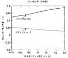
図19は、VBL=1V、Vread=5V、Vr=GND、Vthw=2V、Vthe=−1Vとし、選択トランジスタS1とS2のソース接地時で基板バイアスが0Vの場合のしきい値を0.5Vとし、βSL=2.5βcellとした場合の、電圧VSSLに対する、図41及び図42で説明した4つの読み出し状態の読み出し電流ID1〜ID4を示したものである。但し、基板バイアス効果定数を0.5[V0.5]、ドレイン電圧に対するしきい値低下量(Drain Induced Barrier Lowering定数)を0.49[V/V]としている。
【0149】
図19の右軸は、ID1〜ID4の間での、最大電流/最小電流の比を示している。従来例は、VSSL=5Vの場合に相当する。電圧VSSLをVreadより低下させることにより、最大電流/最小電流の比は小さくなり実施の形態1と同様の効果があることが判る。さらに、最大電流/最小電流比が減少する効果は、VSSL<2.5[V]で大きく増加しており、この条件で臨界的な振る舞いをすることが判る。また、従来、フラッシュNANDメモリの電源電圧Vccは2.5V以上なので、VGSLを電源電圧以下の設定にすることにより、最大電流/最小電流の比は小さくなり上述の効果が大きくなることが判る。
【0150】
図20は、図44(a)のシーケンスによるメモリセルM0の消去しきい値上昇を実線で、図44(b)のシーケンスによるメモリセルM15の消去しきい値上昇を点線で示す。これら電圧関係は、図19と同じものを用いている。電圧VSSLをパス電圧Vreadより低下させても、メモリセルM0およびM15のしきい値上昇量は殆ど変化がなく、従来のようなしきい値上昇量の増大という弊害はない。
【0151】
またこの実施の形態の場合、VSSLを低下させることにより、ID1からID4のなかで最大の電流ID3を減少させることができる。これにより、読み出し時間の最大値を一定としたままで、セル読み出し電流によって生ずる電磁ノイズの最大値を削減することができる。よって、より小さなセル電流を用いても電磁ノイズ、例えば、隣接するデータ転送線間の容量結合による電位変化の影響を受けることなく読み出しを行うことができ、高速でデータ判定をすることができ、電磁ノイズ起因の誤読み出しの確率を減少させ高信頼性を得ることができる。
【0152】
さらに、読み出しセルの最大電流を小さく保つことができるので、共通ソース線SLの電位の浮き上がりが小さくなり、ベリファイ書き込み時に”1”データが”0”データに十分書き込まれない不良が生じにくくなる。また、データ転送線に流れる最大電流も増大するため、電流ストレスによるエレクトロマイグレーションによる配線抵抗上昇が生じず、信頼性劣化も抑えられる。さらに、発熱増大によるトランジスタのしきい値変化やリーク電流の増大の問題も小さくすることができる。
【0153】
なおこの実施の形態において、共通ソース線側の選択ゲート線GSLの電圧は、ビット線側の選択ゲート線の電圧VSSLより高ければ、選択トランジスタS2のコンダクタンスが選択トランジスタS1のそれより大きくなり、効果が得られることは明らかで、選択ゲート線GSLをパス電圧Vreadまで昇圧する必要は必ずしもない。
【0154】
[実施の形態2の変形例]
図21及び図22は、この実施の形態2の変形例として、共通ソース線側からビット線側に読み出し電流を流すようにした場合の動作波形と電圧関係を、図15及び図16に対応させて示している。ここでも、ワード線WL0を選択した場合について示しており、括弧で示しているのは、メモリセルM0の代わりにメモリセルM15を読み出す場合であるが、他のメモリセルM1〜M14も同様の動作で読み出せる。
【0155】
データ読み出し時、データを読み出すブロックのロウデコーダ3およびデータ制御線ドライバ2が活性化され、選択ワード線WL0に読み出し電圧Vr、非選択ワード線WL1〜WL15にパス電圧Vread、選択ゲート線SSLにパス電圧Vreadがそれぞれ印加される(時刻t1)。なお、非選択のブロックのSSL、WL0〜WL15、およびGSLは読み出し期間中フローティングまたは0Vに維持され、データの誤読み出しや破壊が生じないようにする。
【0156】
また以上の電圧印加と同時に、又はこれに先立って、ソース電圧制御回路10を用いて、共通ソース線SLを例えば、GND以上Vcc以下の電圧、VSLに昇圧し、ビット線BLはGNDに放電してその後フローティングにする。ここでVSLとしては、GND以上Vcc以下となることがセンスアンプ回路を構成するトランジスタの信頼性をVcc程度で保証すればよいので望ましい。また、センスアンプトランジスタとしてnチャネルMISFETを用いた場合には、そのしきい値以上とすることがセンスアンプ感度を向上させるのに望ましく、例えば、2V程度とする。
【0157】
読み出し電圧Vrは、例えば、“0”データ書込み後のしきい値下限値をVthw2、“1”データのしきい値上限値をVtheとして、Vthw2とVtheとの範囲内となる値であり、(Vthw2+Vthe)/2程度となることが、最も読み出しマージンを得るのに望ましく、例えば−0.5Vから4Vの間に設定される。特に、Vtheが負で、Vthw2が正となるように設定すれば、VrをGNDに設定でき、Vr発生回路11dが不要となるので望ましい。
【0158】
また読み出し電圧Vrとしては、GND以上の電圧となるように設定することが望ましい。これにより、データ制御線ドライバ2のワード線WL0〜WL15に接続されたトランジスタ拡散層に負電圧を印加されることが無くなり、負電圧発生回路が不要となる。よって、データ制御線ドライバ2のnチャネルMISFETが形成されたp型ウェル電圧をGNDとしp型基板21とn型ウェルで分離することなく形成することができる。よって、データ制御線ドライバ2の回路面積を減少させることができる。さらに、負電圧が印加されないので、n型拡散層が順バイアスされることによる少数キャリア注入が生じなくなり、ラッチアップを防ぐことができる。また、ワード線WL0〜WL15とメモリセルアレイ1内で短絡不良が生じても、メモリセルアレイ1のp型ウェル23やn型拡散層30に負電圧が印加されることがないので、少数キャリア注入による読み出しデータ破壊が生じることもない。
【0159】
非選択メモリセルにつながるワード線WL1〜WL15は、Vread発生回路11cから出力される、メモリセルのしきい値の最大値よりも高い電圧Vreadに設定され、ビット線BL側の選択ゲート線SSLにもVreadが与えられる。
【0160】
本実施の形態では、選択トランジスタS1,S2のゲート電極幅は、メモリセルM0〜M15の制御ゲート電極線幅よりも大きい。一方これらのゲート電極材料であるCoSiやTiSiでは、線幅が小さくなると抵抗が上昇する細線効果が存在することが知られている。よって、この場合、選択トランジスタS1,S2の方がメモリセルM0〜M15よりもゲートが低抵抗となり、選択トランジスタS1の方がメモリセルM0〜M15より高速にVreadまで昇圧することができる。
【0161】
また、ワード線WL0〜WL15を駆動するよりも抵抗の小さい選択トランジスタS1をビット線チャージ期間に駆動することによって、並列に接続されたメモリセルの読み出しタイミングのばらつきを低減することができる。このようにすることにより、メモリセルM0が“1”、すなわち消去状態の場合には、選択トランジスタS2からメモリセルM0〜M15までのソース、ドレイン及びチャネル領域をVSLに充電する。即ち時刻t0から時刻t1までは、共通ソース線SLおよびNANDセルユニット20を充電する共通ソース線(SL)プリチャージ期間に当たる。
【0162】
SLプリチャージ期間は、ワード線WL1〜WL15が十分Vreadに昇圧するまでの時間以上必要であり、例えば100nSから10uSの間の時間とする。ついで、共通ソース線SL側の選択ゲート線GSLをVSSLなる正の電圧にする(時刻t2)。ここで、VSSLは、選択トランジスタS2のしきい値電圧上限Vth以上で、Vread以下の電圧とする。これにより、メモリセルM0のしきい値がVr以下ならば、共通ソース線SLとビット線BLが導通状態となり、ビット線BLの電位はGNDから上昇する。
【0163】
メモリセルM0のしきい値がVrより高い(“0”データ)ならばメモリセルM0は遮断状態となるため、ビット線BLの電位上昇はない。時刻t2からt3までは、ビット線BLをメモリセルM0のデータが“1”の場合に充電を行う、ビット線(BL)チャージ期間となる。このBLチャージ期間は、ビット線BLが十分充電するまでの時間以上必要であり、例えば100nSから100uSの間の時間とする。
【0164】
時刻t3の後、ビット線BLの電位をセンスアンプ回路4で判定し、データをデータラッチに読み出す。この際例えば、特開P2000−76882に示しているように、データ転送線に対する電圧クランプ回路を用いれば、ビット線BLの電位を大幅に変化させなくてもデータを高感度で読み出すことができる。勿論、ここには、センスアンプに電流センス型の回路を用いても同様に読み出すことができるのは明らかである。時刻t3からt4までは、メモリセルM0のデータをセンスするセンス期間に当たる。さらに、SSL、WL0〜WL15、GSL,BLの電位を初期値の例えばGNDに回復するリカバリ期間が存在する。
【0165】
この変形例では、実施の形態2と対照的に、読み出し電流の流れる方向が逆であるから、共通ソース線SL側の選択トランジスタS2について、そのゲート電圧を他のパス電圧Vreadより低い値にすることにより、上の実施の形態2で説明したと同様の効果が得られる。またこの場合、選択ゲート線SSLの電圧は(VGSL+VSL)より高ければ、選択トランジスタS1のコンダクタンスが選択トランジスタS2のコンダクタンスより大きくなり、実施の形態2の効果が得られることは明らかで、選択ゲート線SSLをVreadまで昇圧する必要は必ずしもない。
【0166】
[実施の形態3]
図23及び図24は、この発明の実施の形態3によるメモリセルアレイの構造を示している。この実施の形態ではメモリセル構造として、浮遊ゲート型ではなく、MONOS型を用いている。セルアレイの平面図は図4(b)と同じであり、図23及び図24はそれぞれ、図4(b)のA−A’断面及びB−B’断面を示している。
【0167】
セルアレイは、p型シリコン基板21のn型ウェル22に形成されたp型ウェル23内に形成されている。p型ウェル23は例えば、ボロン濃度が1014cm-3から1019cm-3の間に設定されている。p型ウェル23は、n型シリコン領域22によってp型シリコン基板21とは分離されて、独立に電圧印加できるようになっており、これが消去時の昇圧回路負荷を減らし消費電力を抑える。
【0168】
この実施の形態の場合、メモリセルM0〜M15のゲート絶縁膜は、p型ウェル23の表面に、1nmから10nmの厚さのシリコン酸化膜又はオキシナイトライド膜からなるトンネル絶縁膜25を介して、例えばSiN、SiONからなる電荷蓄積層51が3nmから50nmの厚さで形成されている。この上に、例えば、厚さ2nmから10nmの間のシリコン酸化膜からなる層間絶縁膜52を積層して、ONO構造となっている。選択トランジスタS1,S2については、メモリセルと異なる膜厚のゲート絶縁膜25(GSL),25(SSL)を有する。
【0169】
これらのゲート絶縁膜上に、多結晶シリコンからなるゲート電極28,28(GSL),28(SSL)が形成されている。これらのゲート電極は、素子領域のみに配置された第1層多結晶シリコン膜と、これに重ねてワード線WL0〜WL15及び選択ゲート線GSL,SSLとして連続する第2層多結晶シリコン層の二層構造を有する。
【0170】
この構造は、p型ウェル23上に全面的にゲート絶縁膜25を介して第1層多結晶シリコン膜を堆積した後、これをパターニングし、更にp型ウェル23を例えば0.05〜0.5umの深さエッチングし、素子分離絶縁膜24を埋め込み、その後第2層多結晶シリコン膜の堆積とパターニングを行うことで得られる。
【0171】
この実施の形態のゲート形状でも、上面はシリコン窒化膜29aで覆われ、両側面も例えば5nmから200nmの厚さのシリコン窒化膜(またはシリコン酸化膜)からなる側壁絶縁膜29bが形成される。そしてゲート電極に自己整合的にソース,ドレインとなるn型拡散層30が形成されている。メモリセルのゲート長としては、0.5um以下0.01um以上とする。ソース,ドレインのn型拡散層30としては、例えばリンや砒素、アンチモンを表面濃度が1017cm-3から1021cm-3となるように深さ10nmから500nmの間で形成されている。さらに、これらn型拡散層30は隣接するメモリセル同士共有され、NANDセルユニットが実現されている。
【0172】
この実施の形態において、選択トランジスタS1,S2のゲート電極28(SSL),28(GSL)のゲート長(チャネル長)は、メモリセルのゲート長よりも長く、例えば、1um以下0.02um以上として形成している。これによりブロック選択時と非選択時のオンオフ比を大きく確保でき、誤書き込みや誤読み出しを防止できる。
【0173】
NANDセルユニットの両端部のn型拡散層30d,30sのうち、n型拡散層30dは、層間絶縁膜31aに埋め込まれたコンタクトプラグ32を介して中継電極33aに接続され、これが更に層間絶縁膜31bを介してビット線34に接続される。ビット線34は、タングステンやタングステンシリサイド、チタン、チタンナイトライド、アルミニウム等により形成され、セルアレイのカラム方向に連続的に配設される。もう一方のn型拡散層30sはコンタクトプラグ32を介して、中継電極33aと同時に形成された、セルアレイのロウ方向に連続する共通ソース線33bに接続されている。共通ソース線33bには、ビット線34と同じ材料を用いることができる。コンタクトプラグ32には、不純物がドープされた多結晶シリコン、タングステン、タングステンシリサイド、アルミニウム、アルミニウム、チタン、チタンナイトライド等が用いられる。
【0174】
但し、n型拡散層30sをセルアレイ1のロウ方向に連続的に形成して、これを共通ソース線SLとすることもできる。ビット線BLの上はSiO2、SiN、ポリイミド等の絶縁膜保護層35で覆われる。また、図には示していないが、ビット線Bl上に、W,AlやCuからなる上部配線が形成されている。
【0175】
この実施の形態では、MONOS型セルを用いているため、先の実施の形態の浮遊ゲート型セルよりも書き込み電圧および消去電圧を低電圧化することができ、素子分離間隔を狭めゲート絶縁膜厚を薄膜化しても耐圧を維持することができる。よって、高電圧が印加される回路の面積を小さくでき、よりチップ面積を縮小することができる。また、先の実施の形態と比較して、電荷蓄積層を形成するONO膜の厚さを20nm以下に小さくでき、よりゲート形成時のアスペクトを低減でき、ゲート電極の加工形状を向上させ、層間絶縁膜28のゲート間の埋め込みも向上させることができ、より耐圧を向上させることができる。
【0176】
また、浮遊ゲート電極を形成するためのプロセスやスリット作成プロセスが不要であり、製造プロセスを短くすることができる。また、電荷蓄積層が絶縁体であって、電荷トラップに電荷が捕獲されるので、放射線に対して電荷が抜けにくく強い耐性を持たせることができる。さらに、電荷蓄積層の側壁絶縁膜が薄膜化しても、捕獲された電荷がすべて抜けてしまうことはなく良好な保持特性を維持できる。さらに、電荷畜積層と半導体素子領域とを合わせずれなく形成することができ、より均一な電荷蓄積層と半導体素子領域との容量を実現できる。これにより、メモリセルの容量ばらつきやメモリセル間の容量ばらつきを低減することができる。
【0177】
この実施の形態のセルアレイ構造を用いた場合にも、先の実施の形態1,2で説明したデータ読み出しを行うことにより、実施の形態1,2と同様の効果が得られる。
この実施の形態では選択トランジスタS1およびS2はメモリセルと異なり、電荷蓄積層のないMISFETとしたが、メモリセルと同様のMONOS構造として形成してもよい。また、メモリセルの電荷蓄積層は絶縁体により形成されているので、メモリセル間を分離する側壁絶縁膜は必ずしも必要がない。
【0178】
[実施の形態4]
次に、データ読み出しに際して、NANDセル内の選択ワード線の位置に応じて、選択トランジスタS2のゲート電極(選択ゲート線GSL)に与える電圧VGSLを切り換えるようにした実施の形態を説明する。基本的なEEPROM構成は、実施の形態1或いは実施の形態3と同様であるが、選択ゲート線GSLに与える電圧を切り換えるために、図1の構成に加えて、図25に示すように、Vread/VGSL切り換え回路12が設けられる。
【0179】
切り換え回路12の出力は、メモリセルアレイ1の選択ゲート線GSLに接続されるもので、アドレスバッファ6から出力される内部アドレスに応じて、ワード線WL15からWL(15−x)の範囲が選択された時には、電圧VGSLを出力し、ワード線WL(15−x−1)からWL0の範囲が選択された時には、電圧Vreadを出力する。ここで、xは、0以上で14以下の整数である。データ読み出し動作タイミングは、実施の形態1と変わらない。
【0180】
図26は、この実施の形態による読み出しと従来例による読み出しの場合の読み出し電流変動のワード線位置依存性を示している。具体的な読み出し条件は、基本的には実施の形態1に準じて、VBL=1V、Vread=5V、Vr=GND、Vthw=2V、Vthe=−1V、VSSL=1.8Vとしている。選択トランジスタS1,S2の.ソース接地で基板バイアスが0Vの場合のしきい値は0.5Vである。
【0181】
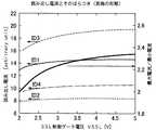
またこのデータは、共通ソース線SL側から順次書き込みと書き込みベリファイ読み出しを行った場合の、ベリファイ読み出し時の電流についてであり、○と□は従来通り、選択ゲート線GSLをVread=5Vに固定した場合である。●と■は、この実施の形態で、x=3とした場合、つまり、ワード線WL15−WL12までが選択された場合にはVGSL=1.8Vを与え、ワード線WL11−WL0までが選択された場合にはVread=5Vを与えた場合を示している。
【0182】
□と■は、選択セルより共通ソース線SL側のメモリセルがオール“1”の場合(最大セル電流)、○と●は、選択セルより共通ソース線SL側のメモリセルがオール“0”の場合(最小セル電流)である。
【0183】
図26から、ワード線WL0が選択された場合に、セル電流は最も小さくなる。これは、実施の形態で説明したように、選択セルのソース側に非選択セルが全て接続されて、大きな基板バイアスがかかるためである。そしてワード線WL15が選択された時にセル電流は最大になる。
【0184】
そしてこの実施の形態の場合、ワード線WL15を選択した場合には、選択ゲート線GSLには、Vccより低いVGSL=1.8Vを与えており、選択トランジスタS2のコンダクタンスを、Vread=5Vを与えた場合より低下させるいる結果、最大セル電流が低下している。ワード線WL0を選択した場合は、従来と同様に、選択ゲート線GSLには、Vead=5Vを与えており、従来と同じ最小セル電流を保っている。
【0185】
以上によりこの実施の形態によれば、図26に示したように、メモリセルに流れる最大電流と最小電流の差(最大電流変動幅)を小さくすることができる。これにより、読み出し時間の最大値を一定に保ったまま、読み出し電流により生じる電磁ノイズの最大値を低減することができる。よって、より小さなセル電流を用いても電磁ノイズ、例えば、隣接するデータ転送線間の容量結合による電位変化の影響を受けることなく読み出しを行うことができ、高速でデータ判定をすることができ、電磁ノイズ起因の誤読み出しの確率を減少させ高信頼性を得ることができる。
【0186】
また、読み出しセルの最大電流を小さく保つことができるので、共通ソース線SLの電位の浮き上がりが小さくなり、ベリファイ書き込み時に”1”データが”0”データに十分書き込まれない不良が生じにくくなる。また、データ転送線に流れる最大電流も増大するため、電流ストレスによるエレクトロマイグレーションによる配線抵抗上昇が生じず、信頼性劣化も抑えられる。さらに、発熱増大によるトランジスタのしきい値変化やリーク電流の増大の問題も小さくすることができる。読み出し電流の最小値は従来と同じに保つことができるので、読み出し時間の増大も生じない。
【0187】
図27は、同実施の形態での選択セル以外の非選択セルの状態による、選択セルのしきい値変動を、図26と対応させて示す。図から明らかなように、この実施の形態によると、ワード線位置によるしきい値変動の幅は、従来例より小さくなり、最小セル電流を従来例と同じに保ちながら最大セル電流を減少させる効果としきい値変動を抑える効果が両立できることがわかる。また、実施の形態では、読み出し電圧Vrは従来と同じGNDであり、“0”書き込みデータとの分離が困難になることはなく、しきい値分布を従来と同じに設定しながら、安定したデータ読み出しが可能になる。
【0188】
図26及び図27は、x=3とした場合のデータであるが、これらの図から、x=1,2,3いずれの場合も同様の効果が得られることは明らかである。
また、実施の形態1の変形例として説明したように、ビット線側の選択トランジスタS1のゲート電圧VSSLをパス電圧Vreadより低くする場合にも、この実施の形態は有効である。この場合、図25の切り換え回路12は、その出力が選択ゲート線SSLに接続されることになる。また切換回路12の切り換え制御は、アドレスバッファ6からのアドレスに応じて、ワード線WL0−WLxまでが選択されるときには、パス電圧Vreadより低いVSSLを出力し、ワード線WL(x+1)−WL15までが選択されるときには、パス電圧Vreadが出力されるようにすればよい。
【0189】
またこの実施の形態4は、メモリセル構造として、実施の形態1,3のいずれを用いた場合にももちろん有効である。
【0190】
[実施の形態5]
NAND型EEPROMにおいては、前述のように、データ読み出し時、選択セルに直列に接続された非選択セルは、しきい値に依らず導通状態を保つ必要があり、書き込みしきい値上限より高い電圧とソース電位との和を、非選択セルの制御ゲートにパス電圧印加する必要がある。このとき、パス電圧のために、非選択セルには書き込みストレスがかかり、誤書き込みが生じてしまう。この現象は、read disturbと呼ばれる。
この実施の形態5は、データ読み出しモードにおける、read disturbを抑制するに好ましい非選択セルの制御ゲートの電圧関係を規定するものである。図28はこの実施の形態5のEEPROM構成を、図1の構成と対応させて示している。図1と対応する部分は、同一符号を付して詳細な説明は省く。また、セルレイアウトや回路構成、素子構造も、実施の形態1或いは実施の形態3と同じである。
【0191】
この実施の形態において、図1と異なる点は、第1に、内部電圧発生回路11が、Vread2発生回路11fを有することである。即ち、データ読み出し時に非選択セルの制御ゲート(ワード線)に与えられるパス電圧Vreadを発生するVread発生回路11cとは別に、パス電圧Vreadよりも低いもう一つのパス電圧Vread2を発生するVread2発生回路11fが付加されている。
【0192】
第2に、図1におけるデータ制御線ドライバ2に対して、メモリセルアレイ1のブロック毎にデータ線ドライバブロック2a,2bを設けて、ロウデコーダ3は、ブロック選択を行うデコーダ3aと、ブロック内のデータ選択線制御を行うブロック内デコーダ(ブロック内データ選択線制御回路)3bにより構成していることである。ブロック内デコーダ3bは、その出力が複数のデータ選択線ドライバ2a,2bに並列に接続され、アドレスバッファ6からの入力によって、従来例でVreadを印加されていたデータ選択線の電圧を読み出し位置によって、VreadとVread2のどちらかの電圧を与えるようにする。具体的には、選択メモリセルよりソース線SL側に位置する非選択メモリセルの制御ゲート電極には、パス電圧Vread2を、選択メモリセルよりビット線BL側にある非選択メモリセルの制御ゲート電極に、パス電圧Vreadを与えるものとする。
【0193】
上述のように、ブロック内デコーダ3bの出力を複数のブロックで共有する構成を取ることにより、メモリブロックそれぞれにデータ選択線制御回路を設ける構成よりも、データ選択線制御回路の回路面積を縮小することができ、より高密度なメモリ回路が実現できる。図28では、わかりやすくするために、メモリセルアレイを破線で示すように2ブロックに分割した場合を示したが、これは2以上の勿論複数ブロックであればよく、それぞれにデータ制御線ドライバ2が形成される構成とすればよい。
【0194】
Vread2発生回路11fは、Vread発生回路11cと同様の構成とし、Vread−Vread2は、読み出し時のビット線BLと共通ソース線SLの最大電位差の絶対値であるVBL以下で且つ、0V(GND)以上とする。Vread−Vread2は、さらに望ましくは、選択メモリセルのセル電流の大小による基準電位線の電位変動の上限値、例えば0.1Vより大きく、VBL以下の範囲に設定する。これにより、共通ソース線の電位変動に依らずこの実施の形態の効果が期待できる。
【0195】
図29は、この実施の形態のデータ読み出し動作時のメモリセルブロック内の電圧関係を示す。メモリブロック内の構成については、実施の形態1と同様なので説明は省略する。ここで、16本のワード線WL0〜WL15のうち、あるワード線WLxに接続されたメモリセルを読み出す場合を考える。データ読み出し時にビット線BLから共通ソース線SLに電流を流す構成では、選択メモリセルのドレイン側にあるワード線WL0〜WL(x−1)には、パス電圧Vreadを与え、選択メモリセルのソース側にあるワード線WL(x+1)〜WL15には、パス電圧Vreadよりも低いパス電圧Vread2を与える。ここで、xは1以上で14以下の整数とする。
【0196】
具体的に、x=14、即ちワード線WL14が選択され、メモリセルM14が選択された場合の動作を、図29及び図30を用いて説明する。なお図29において、括弧内は、メモリセルM1が選択された場合の電圧関係を示している。データ読み出し時、データを読み出すブロックに対応するロウデコーダ及びデータ制御線ドライバ2が活性化され、時刻t0でビット線側の選択ゲート線SSLにパス電圧Vread、非選択ワード線WL0〜WL13にパス電圧Vread、選択ワード線WL14に読み出し電圧Vr、非選択ワード線WL15にパス電圧Vread2が与えられ、時刻t1でビット線BLがVBLにプリチャージされる。この間、ソース側の選択ゲート線GSLはGNDであり、時刻t2で、共通ソース線側の選択ゲート線GSLに、VGSLなる電圧が印加される。これにより、選択セルがデータ“0”の場合は、ビット線が放電されず、選択セルが“1”の場合はビット線放電が行われる。
【0197】
読み出し電圧Vrは、例えば、書込み後のしきい値の最低値をVthw2、消去後のしきい値の最大値をVtheとして、Vthw2とVtheとの範囲内となる値であり、(Vthw2+Vthe)/2程度となることが、最も読み出しマージンを得るのに望ましい。具体的には、Vr=−0.5V〜4Vの間に設定される。なお、非選択のブロックのSSL、WL0〜WL15、およびGSLは読み出し期間中フローティングまたは0Vに保持され、データの誤読み出しや破壊が生じないようにする。
【0198】
読み出し電圧Vrは、消去しきい値Vtheが負で、書き込みしきし値Vthw2が正となるように設定すれば、GNDに設定でき、Vr発生回路11dが不要となるので望ましい。また、読み出し電圧Vrとしては、GND以上の電圧となるように設定すれば、データ制御線ドライバ2のワード線WL0〜WL15に接続されたトランジスタの拡散層に負電圧を印加されることが無くなり、負電圧発生回路が不要となる。このため、データ制御線ドライバ2のn型MISFETが形成されたp型Well電圧をGNDとしp型基板21とn型領域で分離することなく形成することができる。これにより、データ制御線ドライバ2の回路面積を減少させることができる。さらに、負電圧が印加されないので、拡散層が順バイアスされることによる少数キャリア注入が生じなくなり、ラッチアップを防ぐことができる。
【0199】
また、ワード線WL0〜WL15とメモリセルアレイ1内で短絡不良が生じても、メモリセルアレイ1のp型Well23やn型拡散層30に負電圧が印加されることがないので、少数キャリア注入による読み出しデータ破壊が生じることもない。残りの非選択メモリセルにつながるワード線WL0〜WL13は、図30に示したように、Vread発生回路11cから出力される、(メモリセルの書込みしきい値の最大値)+VBLよりも高い電圧に設定され、ビット線側の選択線SSLにもVreadが与えられる。
【0200】
この実施の形態で特徴的なことは、データを読み出す選択セルから電流が流れ出す方向、つまり選択セルのソース側に接続された非選択セルの制御ゲート、この場合ワード線WL15には、ドレイン側での非選択セルのパス電圧Vreadよりも低いパス電圧Vread2が与えられることである。この様に非選択セルに与えるパス電圧を使い分けることによる効果を、以下、メモリセルのドレインコンダクタンスが小さい場合と大きい場合について説明する。
【0201】
選択セルのドレインコンダクタンスが非選択セルや選択トランジスタのドレインコンダクタンスよりも十分低く、選択セルが飽和領域で動作する場合には、ビット線と共通ソース線間の電圧の大部分が選択セルのソース電極とドレイン電極との間に印加される。このため、選択セルのソース電極の電位はドレイン電極の電位よりも大きく低下する。すなわち、選択メモリセルのソース側に接続された非選択メモリセルのソース,ドレインの電位は、選択メモリセルのドレイン側に接続された非選択メモリセルのソース,ドレインの電位よりも共通ソース線の電位GNDに近くなる。
【0202】
一方、最もビット線に近いメモリセルM0のソース電位はほぼVBLとなり、最も共通ソース線に近いメモリセルM15のソース電位はGNDである。従って、もし従来のように、パス電圧Vreadが全て同じであるとすると、非選択セルが全て消去状態にあるとしてその非選択セルの誤書き込みストレスは、メモリセルM0ではほぼVread−VBL、メモリセルM15ではVread−GNDとなり、メモリセルM15のセルの方が大きな誤書き込みストレスが印加される。
【0203】
これに対して、この実施の形態では、パス電圧Vread2を、パス電圧Vreadより低く、例えばVread−VBL以上と設定する。これにより、メモリセルM15の誤書き込みストレスを効果的に削減することができる。
【0204】
また、読み出しメモリセルのドレインコンダクタンスが直列非選択セルや選択スイッチングトランジスタのドレインコンダクタンスよりも十分低く、読み出しメモリセルが飽和領域で動作するものとする。この場合には、メモリセルM0に関するソースドレイン電極から測定したゲート電圧は従来例と同じくほぼVread−VBLとなり、M15よりも誤書き込みストレスが印加されることなく良好なデータ保持特性が保たれる。
【0205】
さらに、選択メモリセルのドレインコンダクタンスが非選択メモリセルのドレインコンダクタンスと同程度以上となった場合には、実施の形態1で説明したのと同様の方法によって、選択スイッチングトランジスタS2のドレインコンダクタンスを非選択セルのドレインコンダクタンスよりも小さくする。これにより、非選択メモリセルの記憶状態がいずれの場合でも、この実施の形態の構成で読み出しに伴う誤書き込みストレスをさらに削減できることを本発明者らは新たに見出した。以下にこれについて説明する。
【0206】
例えば、選択メモリセルがM14であり、非選択メモリセルM0〜M12はデータ“0”(すなわち、書き込み状態)でドレインコンダクタンスが低く、メモリセルM13,M15はデータ“1”(すなわち、消去状態)でドレインコンダクタンスが高く、選択メモリセルM14も消去状態”1”でドレインコンダクタンスが高くなっているとする。このメモリ記憶パターンにおいて、選択メモリセルのドレインコンダクタンスが、非選択セルのドレインコンダクタンスと同程度以上で且つ線形領域で動作しているとして、共通ソース線側の選択ゲート線電圧VGSLをVreadに設定したとする。
【0207】
このとき、ビット線BLと共通ソース線SL(基準電位線)との間の電位差は、ドレインコンダクタンスの低いメモリセルセル部分、すなわちメモリセルM0からM12に集中的に印加される。これにより、図29に示す選択メモリセルM14のドレインノード(即ち非選択メモリセルM13のソースノード)の電位V1もほぼGNDとなる。この結果、非選択メモリセルM13の誤書き込みストレスはVread−GNDとなり、従来例と同じ高い誤書き込み電圧ストレスが非選択メモリセルM13に印加される。
【0208】
これに対してこの実施の形態において、実施の形態1で説明したと同様に、VGSLをVccよりも低く保つと、選択スイッチング素子(MISFET)S2がセル電流が増加した場合の電流制限素子として動作する。このため、選択メモリセルのドレインコンダクタンスが直列非選択セルのドレインコンダクタンスと同程度以上となった場合、セル電流が増加し選択トランジスタS2のドレインおよびソース間の電圧降下が増加するため、非選択メモリセルM13のソースノード(図29のV1ノード)がGND以上VBL以下に上昇する。これにより、非選択メモリセルM13の誤書き込みストレスはVread−GNDよりも小さくなる。
【0209】
図30には、上述した非選択メモリセルM13のソースであるV1ノードの電位変化を、併せて示した。図30の一点鎖線は、VGSLがVcc以上の場合で、実線がVGSLがVcc以下の場合である。メモリセルM13よりも読み出し電流が流れる方向の上流に位置する非選択メモリセルM0−M12の誤書き込みストレスも当然に、従来例よりも小さくなる。
【0210】
選択トランジスタS2のドレインコンダクタンスを、選択セルのしきい値電流(しきい値電圧近傍でのセル電流)におけるドレインコンダクタンスよりも大きく、例えば3倍以上と設定すれば、しきい値電流と同程度のセル電流の場合には、ビット線BLと共通ソース線SL(基準電位線)との間の電位差は、選択セルのドレインおよびソース間に7割以上印加される。従って選択トランジスタS2によりセル電流が減少するという影響は、ごく僅かである。これは、選択トランジスタS2が単なる線形抵抗ではなく、一定電流以上で等価抵抗が非常に大きく、一定電流以下では等価抵抗が非常に小さい抵抗素子として働くことによる。従って、読み出しの最小電流は、従来例とほぼ同じく保つことができる。
【0211】
特に、セル電流の大小を電流基準値(参照電流値)と比較してデータ判定するセンス方式を用いる場合には、選択メモリセルのドレインコンダクタンスが直列非選択セルのドレインコンダクタンスと同程度以上では、しきい値電流よりも大きなセル電流となることは明白である。よって、選択トランジスタのドレインコンダクタンスが本実施の形態のように従来例よりも小さくなっても、それが選択メモリセルの電流しきい値におけるドレインコンダクタンスよりも十分大きな場合には、読み出しデータが”1”の場合のセル電流の最小値が保持され、しきい値判定には問題が生じない。勿論、同時に、バックパターンによるセル電流の増大は抑えることができるので、セル電流の変動は従来よりも抑制することができる。
【0212】
一方、この実施の形態の方法を用いることにより、メモリセルに流れる最大電流と最小電流との差を小さくすることができる。従って、読み出し時間の最大値を一定としたままで、セル読み出し電流によって生ずる電磁ノイズの最大値を削減することができる。これにより、より小さなセル電流を用いても電磁ノイズ、例えば、隣接するビット線間の容量結合による電位変化の影響を受けることなく読み出しを行うことができる。これは、高速でのデータ判定を可能とし、電磁ノイズ起因の誤読み出しの確率を減少させた高信頼性を得ることを可能とする。
【0213】
さらに、選択セルの最大電流を小さく保つことができるので、共通ソース線SLの電位の浮き上がりが小さくなる。これは、ベリファイ書き込み時に”1”データが”0”データに十分書き込まれないという不良の発生を防止する。また、ビット線に流れる最大電流も減少するため、電流ストレスによるエレクトロマイグレーションによる配線抵抗上昇が生じず、信頼性劣化も抑えられる。さらに、発熱増大によるトランジスタのしきい値変化やリーク電流の増大の問題も小さくすることができる。また、読み出し電流の最小値は従来と同じに保つことができるので、最小の読み出し電流が減少することによる読み出し時間の増大も生じない。
【0214】
さらに、選択メモリセルに直列に接続された非選択メモリセルの、読み出し時の誤書き込みストレスを低減することができるので、データの”1”データと”0”データとの電圧マージンを削減できる。よって、パス電圧Vreadをさらに下げることができるので、パス電圧Vreadを発生するための昇圧回路面積や昇圧時間を低減することができ、より信頼性の高いメモリを実現することができる。
選択ゲート線電圧VGSLをVccよりも低くした構成では、実施の形態1で説明した利点が同様に存在するのは言うまでもない。
【0215】
[実施の形態6]
図31は、本発明の実施の形態6のデータ読み出し動作時のメモリセルブロック内の構成、および電圧関係を示す。EEPROM全体の構成は、先の実施の形態5の図28と同様である。また、セルレイアウトや回路構成、素子構造も、実施の形態1或いは実施の形態3と同じである。この実施の形態6では、実施の形態5とは読み出し電流の流れる方向が異なり、この点で実施の形態1の変形例と同じになっている。複数のビット線に対してビット線数より少ないセンスアンプが用いられる場合に、図31では、一つのセンスアンプを共有するビット線BLa,BLbの部分が示されている。
【0216】
ここでは、一方のビット線BLbに接続されたメモリセルをセンスアンプで読み出し、非選択状態の他方のビット線BLaは読み出し時に例えば、共通ソース線SLと同じ電位に保つことによって、電位変動を抑制するシールド線として動作させることとする。図31では簡単のために、1つのセンスアンプに接続される2本のビット線BLa,BLbのみ示しているが、複数本のビット線が配列されて、読み出しビット線以外のビット線の少なくとも一本をシールド線とすれば、この実施の形態の効果が生じる。
【0217】
特に、シールド効果については、読み出しセルのつながった複数のビット線BLbについて、それぞれの間に少なくとも1本のシールドビット線BLaが存在する、図2で示した構成が、読み出しに伴う、ビット線の容量結合ノイズを削減するには望ましい。そしてこの実施の形態では、シールドビット線に接続されたメモリセルのread disturbも抑制することができる。
【0218】
メモリブロック内の構成については、実施の形態1と同様であるので、説明は省略する。ここでは、16本のワード線WL0〜WL15のうち、ワード線WLxにより駆動されてビット線BLbに接続されたメモリセルを読み出す場合を考える。データ読み出し時に共通ソース線SLからビット線BLへ電流を流すこの実施の形態では、選択メモリセルのドレイン側(先の実施の形態5と電流が逆であるから、共通ソース線SL側がドレインになる)にあるワード線WL(x+1)〜WL15には従来と同様にパス電圧Vreadを与え,選択メモリセルのソース側にあるワード線WL0〜WL(x−1)には、パス電圧Vreadよりも低いパス電圧Vread2を与える。
【0219】
ここで、xは1以上で14以下の整数である。図31では、x=1の場合、即ちワード線WL1によりメモリセルM1が選択された場合の電圧関係を示し、図32はその読み出し動作のタイミング図を示している。なお図31の括弧内は、メモリセルM1の代わりにメモリセルM14が選択されたときの電圧関係を示している。他のメモリセルが選択された場合も、選択セルのドレイン側とソース側の非選択セルに与えられるパス電圧の関係は、同様に設定される。
【0220】
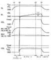
データ読み出し時、ブロック選択デコーダ3a及びブロック内選択デコーダ3bによって、データを読み出すブロックのデータ制御線ドライバ2が活性化される。まず時刻t0で、共通ソース線側の選択ゲート線GSL、非選択ワード線WL2−WL15にパス電圧Vreadを、選択ワード線WL1に読み出し電圧Vrを、非選択ワード線WL0にはパス電圧Vreadより低いパス電圧Vread2をそれぞれ与える。そして、時刻t1で、共通ソース線SL及び非選択ビット線BLaに電圧VSLを与える。その後、時刻t2でビット線側の選択ゲート線SSLに電圧VGSLを与えることにより、選択ビット線BLbは、読み出しデータに応じて、共通ソース線SL側からの電流により充電され(データ“1”のとき)、或いは充電されない(データ“0”のとき)。
【0221】
なお非選択のブロックのSSL、WL0〜WL15、およびGSLは読み出し期間中フローティングまたは0Vに保持され、データの誤読み出しや破壊が生じないようにする。
読み出し電圧Vrは、書込み後のしきい値の最低値をVthw2、消去後のしきい値の最大値をVtheとして、Vthw2とVtheとの範囲内となる値であり、(Vthw2+Vthe)/2程度となることが、最も読み出しマージンを得るのに望ましい。具体的に例えば読み出し電圧Vrは、−0.5Vから4Vの間に設定される。Vtheが負で、Vthw2が正となるように設定すれば、読み出し電圧VrをGNDに設定でき、Vr発生回路11dが不要となるので望ましい。
【0222】
また、読み出し電圧Vrとしては、GND以上の電圧となるように設定することが望ましい。これにより、データ制御線ドライバ2のワード線WL0〜WL15に接続されたトランジスタの拡散層に負電圧を印加されることが無くなり、負電圧発生回路が不要となる。更に、データ制御線ドライバ2のn型MISFETが形成されたp型Well電圧をGNDとしp型基板21とn型領域で分離することなく形成することができる。この結果、データ制御線ドライバ2の回路面積を減少させることができる。また、負電圧が印加されないので、拡散層が順バイアスされることによる少数キャリア注入が生じなくなり、ラッチアップを防ぐことができる。
【0223】
また、ワード線WL0〜WL15とメモリセルアレイ1内で短絡不良が生じても、メモリセルアレイ1のp型Well23やn型拡散層30に負電圧が印加されることがないので、少数キャリア注入による読み出しデータ破壊が生じることもない。残りの非選択メモリセルにつながるワード線WL2〜WL15は、図28に示したように、Vread発生回路11cから出力される、メモリセルの書込みしきい値の最大値よりも高い電圧に設定され、共通ソース線に接続された側の選択ゲート線GSLにもパス電圧Vreadが与えられる。
【0224】
この実施の形態で特徴的なことは、データを読み出す選択セルから電流が流れ出す方向、つまりソース側に接続された非選択セルのゲート電極、この場合ワード線WL0には、パス電圧Vreadよりも低いパス電圧Vread2が与えられることである。以下、メモリセルのドレインコンダクタンスが小さい場合と大きい場合に分けてこの実施の形態の効果を説明する。
【0225】
まず、データを読み出す選択メモリセルのドレインコンダクタンスが直列非選択セルや選択トランジスタのドレインコンダクタンスよりも十分低く、読み出しメモリセルが飽和領域で動作するものとする。このとき、ビット線と共通ソース線間の電圧の大部分が選択セルのソース電極とドレイン電極との間に印加され、選択メモリセルのソース電極の電位はドレイン電極の電位よりも大きく低下する。すなわち、選択メモリセルのソース側に接続された非選択メモリセルのソース,ドレイン電極の電位は、選択メモリセルのドレイン側に接続された非選択メモリセルのソース,ドレイン電極の電位よりも共通ソース線に与えられる電位VSLに近くなる。
【0226】
一方、最もビット線BL側に配置された非選択メモリセルM0のソース電位はほぼGNDとなり、最も共通ソース線SL側に配置された非選択メモリセルM15のソース電位はVSLとなる。もし、非選択セルが全て消去状態であるとして、これらに同じパス電圧Vreadが与えられたとすると、非選択セルの誤書き込みストレスは、メモリセルM15ではほぼVread−VSL、メモリセルM0ではVread−GNDとなり、メモリセルM0の方に大きな誤書き込みストレスがかかる。
【0227】
これに対して、この実施の形態では、例えばパス電圧Vread2を、パス電圧Vread以下でVread−VSL以上と設定することにより、非選択メモリセルM0での誤書き込みストレスを効果的に削減することができる。また、選択メモリセルのドレインコンダクタンスが直列非選択セルや選択トランジスタのドレインコンダクタンスよりも十分低く、且つ選択メモリセルが飽和領域で動作する場合には、非選択メモリセルM15に関するソース,ドレイン電極から測定したゲート電圧は従来例と同じくほぼVread−VSLとなり、従来以上に誤書き込みストレスが印加されることなく、良好なデータ保持特性が保たれる。
【0228】
さらに、選択メモリセルのドレインコンダクタンスが直列非選択セルのドレインコンダクタンスと同程度以上となった場合には、実施の形態1で説明したのと同様の方法によって、選択トランジスタS1のドレインコンダクタンスを非選択セルのドレインコンダクタンスよりも小さくするが有効である。これにより、非選択メモリセルの記憶状態がいずれの場合でも、この実施の形態の構成で誤書き込みストレスをさらに削減できることが明らかになった。以下これについて説明する。
【0229】
例えば、メモリセルM1が選択され、このとき非選択メモリセルM3−M15がデータ“0”(書き込み状態)でドレインコンダクタンスが低く、非選択メモリセルM0とM2がデータ“1”(消去状態)でドレインコンダクタンスが高い場合を考える。選択メモリセルM1は消去状態”1”であるとし、ドレインコンダクタンスが高くなっているとする。更にこの記憶パターンにおいて、選択メモリセルM1のドレインコンダクタンスが直列非選択セルのドレインコンダクタンスと同程度以上となり線形領域で動作しているとする。
【0230】
このときもし、選択ゲート線電圧VGSLをパス電圧Vreadとした場合には、ビット線BLと共通ソース線SL(基準電位線)との間の電位差は、ドレインコンダクタンスの低いセル部分、すなわち非選択セルM3−M15に集中的に印加される。これにより、図31に示す選択セルM1のドレインノード(V2ノード)もほぼGNDとなる。このため、非選択メモリセルM2の誤書き込みストレスはVread−GNDとなり、従来例と同じ高い誤書き込み電圧ストレスがメモリセルM2に印加される。
【0231】
一方、この実施の形態では、実施の形態1の変形例で説明したように、選択ゲート線電圧VGSLをVccよりも低く保つことにより、選択トランジスタS1がセル電流が増加した場合の電流制限素子として動作する。このため、選択セルのドレインコンダクタンスが直列非選択セルのドレインコンダクタンスと同程度以上となった場合、セル電流が増加して選択トランジスタS1のドレインおよびソース間の電圧降下が増加する結果、メモリセルM2のソース電位がGND以上VBL以下に上昇する。これにより、非選択メモリセルM2のソースであるV2ノードも上昇し、非選択メモリセルM2の誤書き込みストレスは常にVread−GNDよりも小さくなる。
【0232】
図32は、上述したV2ノードの変化を示している。図32の一点鎖線は、VGSLがVcc以上の場合で、実線はVGSLがVcc以下の場合である。なお、メモリセルM2よりも読み出し電流が流れる方向の上流に位置するメモリセルM2−M15の誤書き込みストレスも当然に、従来例よりも小さくなる。
【0233】
選択スイッチングトランジスタS1のドレインコンダクタンスを、データを読み出す選択セルのしきい値電流におけるドレインコンダクタンスよりも大きく、例えば3倍以上と設定すれば、しきい値電流と同程度のセル電流の場合には、ビット線BLと共通ソース線SL(基準電位線)との間の電位差は、選択セルのドレインおよびソース間に7割以上印加される。従って、選択トランジスタS1によるセル電流の減少への影響はごく僅かである。これは、選択トランジスタS1が単なる線形抵抗ではなく、一定電流以上で等価抵抗が非常に大きく、一定電流以下では等価抵抗が非常に小さい抵抗素子として働くことによる。つまり、読み出しの最小電流は、従来例とほぼ同じく保つことができる。
【0234】
特に、セル電流の大小を基準電流値と比較してデータ判定するセンス方式を用いる場合には、選択メモリセルのドレインコンダクタンスが直列非選択セルのドレインコンダクタンスと同程度以上となった場合に、しきい値電流よりも大きなセル電流となることは明白である。よって、選択スイッチングトランジスタのドレインコンダクタンスがこの実施の形態のように従来例よりも小さくなっても、選択メモリセルの電流しきい値におけるドレインコンダクタンスよりも十分大きな場合には、読み出しデータが”1”の場合のセル電流の最小値を保持されるため、しきい値判定には問題が生じない。
【0235】
同時に、バックパターンによるセル電流の増大は抑えることができるので、セル電流の変動は従来よりも抑制することができる。ここでバックパターンとは、選択セルに直列接続された非選択セルのしきい値パターン、特にビット線側の非選択セルのしきい値のパターンをいう。ビット線側にある非選択セルの書き込み/消去のデータ状態により、選択セルのドレインとビット線との間に入るコンダクタンスが決定され、これにより選択セルの読み出し電流が決定されることを、本発明者等はバックパターンの影響と呼んでいる。
【0236】
さらに、この実施の形態では、図32のように、シールドビット線BLaには、読み出し時に電位基準線SLと同じ電位VSLが印加される。よって、非選択のシールドビット線BLaに接続されたメモリセルM0’−M15’の誤書き込み電圧ストレスは、最大Vread−VSLとなり、従来例のシールドビット線BLaに接続されたメモリセルに印加されるVread−GNDよりも常に抑制することができる。そして、読み出し時に共通ソース線SLと非選択ビット線BLaは同電位に保っているので、非選択ビット線BLaがシールド線として機能し、複数のビット線BLb間の容量結合ノイズを低減できることは明らかである。
【0237】
またこの実施の形態の方法を用いることにより、メモリセルに流れる最大電流と最小電流との差を小さくすることができ、読み出し時間の最大値を一定としたままで、セル読み出し電流によって生ずる電磁ノイズの最大値を削減することができる。よって、より小さなセル電流を用いても電磁ノイズ、例えば、隣接するビット線間の容量結合による電位変化の影響を受けることなく読み出しを行うことができ、高速でデータ判定をすることができ、電磁ノイズ起因の誤読み出しの確率を減少させ高信頼性を得ることができる。
【0238】
さらに、読み出しセルの最大電流を小さく保つことができるので、電位基準線SLの電位の変動が小さくなり、ドレイン電圧変動に伴うしきい値変動が生じにくくなる。また、ビット線に流れる最大電流も減少するため、電流ストレスによるエレクトロマイグレーションによる配線抵抗上昇が生じず、信頼性劣化も抑えられる。発熱増大によるトランジスタのしきい値変化やリーク電流の増大の問題も小さくすることができる。また、読み出し電流の最小値は従来と同じに保つことができるので、最小の読み出し電流が減少することによる読み出し時間の増大も生じない。
【0239】
さらに、選択メモリセルに直列に接続された非選択メモリセルの、読み出し時の誤書き込みストレスを低減することができるので、データの”1”データと”0”データとの電圧マージンを削減できる。よって、読み出し時のパス電圧Vreadをさらに下げることができるので、パス電圧Vreadを発生する昇圧回路の面積や昇圧時間を低減することができ、より信頼性の高いメモリセルを実現することができる。この実施の形態により、実施の形態1で説明した利点や実施の形態5で説明した利点は同様に存在するのは言うまでもない。
【0240】
[実施の形態7]
図33は、この発明の実施の形態7によるNAND型EEPROMのブロック構成を示す。セルアレイ構成は、図2−8に示したものと変わらない。また素子構造として実施の形態3のものを用いうる。図33は、先の実施の形態6の図28とほぼ同様の構成であるが、VGSL発生回路の出力の切り換えを行う方式に代わって、Vread発生回路11cが、データ読み出し時に選択ページによって、少なくとも2つの異なるパス電圧Vreadを選択出力できるようになっている点に特徴がある。
【0241】
この実施の形態では、データ読み出し時の非選択メモリセルでのしきい値変動を効果的に抑制する手法を提供する。データ読み出し時、選択メモリセルに直列に接続された非選択メモリセルのコンダクタンスが書き込み/消去状態に応じて変化し、その結果として選択メモリセルのしきい値が変化する問題に対しては、原理的には、非選択メモリセルの制御ゲート電圧を上昇させて、非選択メモリセルのドレインコンダクタンスを上昇させればよい。しかし、非選択メモリセルの制御ゲート電圧を余り高くすると、非選択メモリセルは書き込みストレスが印加され、誤書き込み(read disturb)が生じてしまう。
【0242】
この実施の形態は、選択メモリセルのドレイン側に多くの“0”データの非選択メモリセルが接続される状態でのドレインコンダクタンスは低下させずに、read disturbによる非選択メモリセルでの誤書き込みを防止しながら、選択メモリセルのしきい値上昇を減少させる。これは、選択メモリセルでのしきい値上昇を一定にする条件に変更すれば、非選択メモリセルのデータが全てデータ“0”という最悪時のドレインコンダクタンスを上昇させることができるため、従来の課題を解決することができる。
【0243】
この様な目的でこの実施の形態の図33の構成においては、内部電圧発生回路11のVread発生回路11cに、その出力電圧を制御する制御入力として、アドレスバッファ6から選択ページが入力されている。ここで“ページ”とは、1つのNANDセルブロック内で、ワード線WL0〜WL15のそれぞれに接続された複数のメモリセルのグループを指す。
【0244】
図34は、Vread発生回路11cの具体的な構成を示している。リングオシレータ回路101とその発振出力により駆動されるチャージポンプ回路102とが昇圧回路を構成しており、これにより電源電圧を昇圧した高電圧であるパス電圧Vreadが発生される。チャージポンプ回路102の出力端子には、その昇圧動作を制限するための電圧(または電流)モニタ回路103が接続されている。このモニタ回路103は、パス電圧Vreadが定められた値以上に上昇した場合に、チャージポンプ回路102を停止または、駆動力を低下させる制御を行う。このモニタ回路103によって、Vread出力電圧に対して負帰還が形成され、安定した出力電圧を得られるようになっている。
【0245】
リングオシレータ101,チャージポンプ回路102及びモニタ回路103の部分には、公知の回路が用いられる(例えば、特開2000−105998公報)。また、参照電圧(又は参照電流)に応じて異なる昇圧電圧を得るための回路方式として、例えば、複数のチャージポンプ回路を備えてこれを切り換え制御する方式を用いてもよい(例えば、特開平7−111095号公報)。
【0246】
モニタ回路103は、Vread出力を分圧した値と参照電圧とを比較する比較器により構成される。モニタ回路103は、出力パス電圧Vreadを例えば抵抗によって、分圧または分流してから参照電圧や基準電圧と比較する回路を含んでもよい。このようにすることにより、例えば3V以上のVread電圧をフィードバックするモニタ回路103をVreadよりも低電圧の能動素子を用いた回路で構成することができ、より耐圧が小さく面積の小さい能動回路素子を用いることができる。よって、モニタ103の回路面積をより縮小することができる。
【0247】
参照電流を利用する場合には、モニタ回路103は、参照電流と、Vread出力を例えば抵抗分割によって分流した値とを比較器で比較することにより構成される。参照電圧発生回路は、ディジタルデータが入力される論理回路105とその出力をアナログ値に変換するD/A変換回路104を備えて構成される。D/A変換回路104の出力が、Vread電圧を設定するための参照電圧(または参照電流)値となる。
【0248】
論理回路105は、読み出し時に選択したページアドレス信号と、配線層をすべて積層後にその論理値を設定可能なトリミング設定値の二つのディジタル信号を入力として、これらの論理和を作成し出力する。トリミング設定値は、昇圧電圧を最適値に調整するためのデータであって、ウェハテストの結果に応じて例えばフューズやアンチフューズその他の不揮発性メモリに書き込み保持され、メモリの電源投入時に自動的に読み出されて、内部電圧発生回路の調整に用いられるものである。出荷テスト時に、あるページに対するVreadを設定した後は、電源遮断によらず値が保たれるようにすることがVreadを調整後一定範囲に保つため望ましい。
【0249】
図35は、論理回路105の構成例であり、全加算器201を直列接続したいわゆるマンチェスタ型加算器を構成している。A3〜A0は選択ページアドレス信号(ディジタル信号)の信号線であり、B3〜B0はトリミング設定値(ディジタル信号)の信号線である。この様なマンチェスタ型加算器に選択ページアドレス信号とトリミング設定値を入力することにより、C4〜C0には選択ページアドレスとトリミング設定値の和の値をディジタル出力することができる。
【0250】
この様に論理回路105の出力がディジタルで与えられているため、選択ページアドレスからアナログ信号を作成し、トリミング設定値ディジタル入力からアナログ信号を作成し、それらをアナログ信号として足し合わせる場合よりも、ノイズの影響を受けにくくダイナミックレンジを広く確保することができる。また、D/A変換回路104は1つでよいので、選択ページアドレスとトリミング設定値の和に対して、容易に単調性(monotonicity)が保証され、温度変化による特性変化保証も容易である。これにより、設定する電圧ステップが小さくても精度良くVread電圧を設定することができる。
【0251】
なお論理回路105において、A1、A0に例えば、選択ページの上位アドレスのみを割り当て、A3,A2をGNDとすることにより、ワード線を、WL0〜WL3、WL4〜WL7、WL8〜WL11、WL12〜WL15のようにグループに分ければ、グループ毎に異なり、各グループ内では一定のVread電圧を得るようにすることができる。このようにして、選択ページアドレスの差による電圧ステップとトリミング入力の電圧ステップを変えて割り当てることも容易にできる。さらに、選択ページのディジタル値を割り算回路で割ることにより、トリミング入力ステップの任意の整数倍を選択ページのアドレスの差による電圧ステップに割り当てることもできる。
【0252】
次にこの実施の形態におけるデータ読み出し時のメモリセル部分の電圧関係と動作について、図36を用いて説明する。図36では、ワード線WLx(xは0〜15の範囲の整数)が選択された場合のVread発生回路11cが出力するパス電圧を、Vreadxと表している。図36(a)は、最も共通ソース線SLに近いメモリセルM15が選択された場合、同図(b)は、メモリセルM2が選択された場合、同図(c)は最もビット線BLに近いメモリセルM0が選択された場合である。またこの実施の形態では、ビット線BLから共通ソース線SLに読み出し電流を流す。
【0253】
ワード線WL15が選択された図36(a)の場合は、選択メモリセルM15よりビット線BL側に最も多く非選択メモリセルが存在し、ワード線WL0が選択された図36(c)の場合は、選択メモリセルM0よりビット線側には非選択セルはない。そして、図36(a)のとき非選択セルに与えられるパス電圧Vread15と、図36(c)のとき非選択セルに与えられるパス電圧Vread0とは、Vread15>Vread0に設定される。
【0254】
図36(b)は、ワード線WL2が選択された場合であり、このとき非選択セルに与えられるパス電圧Vread2は、Vread15>Vread2>Vread0なる関係に設定される。即ちこの実施の形態では、データを読み出す選択セルよりもビット線BL側に存在する非選択セルの数の増加につれて、非選択セルに与えるパス電圧を上昇させることが特徴である。
より一般的に、ワード線WLxの位置を表す整数xについて、その整数xが任意の値i,jをとるとものとして、i>jとなる場合に、Vreadi≧Vreadjとなることが、read disturbによる消去しきい値上昇を抑制するためには望ましい。
【0255】
この実施の形態は、書き込みベリファイ読み出し動作については、一括消去された後に、共通ソース線側のメモリセルから順にデータ書き込みを行う方式を採用した場合に特に有効である。共通ソース線側のメモリセルから順に書き込みを行うと、選択セルよりも後に書き込むデータによる非選択セルの抵抗変化をドレイン側(ビット線側)のメモリセルだけ考えればよく、ソース側の非選択セルの電圧降下量は変化しないので、ソース電位変化によるしきい値変動を抑制し、選択セルのしきい値変動を小さくすることができるからである。なお、図36に示したように、選択スイッチングトランジスタS1,S2の制御電極に与える電圧はVreadxまたはVccと従来例と同じ値を用いてよいし、勿論、実施の形態6までで述べた方法も併用できる。
【0256】
読み出し選択セルに直列に接続された非選択セルの書き込み/消去状態(即ちバックパターン)に依ってコンダクタンスが変化することに起因する、選択セルのしきい値の最大変化量をΔVth、しきい値電圧を定義する電流(しきい値電流)をIthとしたとき、本発明者らは、選択セル位置を固定した場合に、図38に示すように、Ith/ΔVthが(Vread−Vthw)のほぼ線形関数となることを初めて発見し、その解析モデルを構築した。図38は具体的に、読み出し選択セルを共通ソース線に最も近いM15とし、パス電圧VreadとメモリセルM0〜M15の書き込みしきい値Vthwを様々に変化させた場合のIth/ΔVthを示している。消去しきい値Vtheは−2Vに固定し、Ithは10pA以上2uA以下の範囲内の値を用いている。またパス電圧Vreadは3Vから6Vの範囲内の値を、Vthwは0Vから4Vの範囲内の値を用いている。
【0257】
図38の特性は、次のように説明することができる。選択セルのドレインコンダクタンスが直列非選択セルや選択スイッチングトランジスタのドレインコンダクタンスよりも十分低く且つ、選択セルが飽和領域で動作する場合には、ビット線と共通ソース線の間の電圧の大部分が選択セルのドレインとソースとの間に印加されるため、選択セルのソース電極の電位はドレイン電極の電位よりも大きく低下する。選択セルよりビット線側に接続された非選択セルは、線形動作するものとすると、その一つ当たりのコンダクタンスは、しきい値Vthwの書き込み状態のとき最低であり、V0を定数として、βcell×(Vreadx−Vthw−V0)となる。ビット線側の非選択セルの全体のコンダクタンスは、ビット線側の非選択セルの数nkが増えるほど減少し、基板バイアス効果を無視すれば、ほぼβcell×(Vreadx−Vthw−V0)/nkとなる。
【0258】
非選択セルが消去状態では、そのしきい値はVtheであるから、選択セルに直列に接続されたビット線側の非選択セルの書き込み/消去状態に依ってコンダクタンスが変化することに起因する選択セルのドレイン電圧の変化量ΔVDは、下記数5のように近似できる。
【0259】
【数5】
ΔVth∝ΔVD=(Ith・nk/βcell)[1/(Vreadx-Vthw-V0)−1/(Vreadx-Vthe-V0)]〜Ith・nk/βcell・(Vreadx-Vthw-V0)
【0260】
即ち数5は、例えば、Vthw=1V,Vthe=−2Vとしたとき、中括弧内の第1項に比べて小さい第2項を無視することができ、これによりしきい値変動ΔVthが(Vreadx−Vthw−V0)に逆比例するという近似式が得られることを示している。選択セルのソース側電位は、Ithの一定電流を流している場合には変化しない。従って、ドレイン電圧によるしきい値低下効果(Drain Induced Barrier Lowering)による選択セルのしきい値低下ΔVthは、ΔVDに比例するため、図38の実験特性を説明できることになる。
【0261】
図36において、選択セルよりも上流側の直列非選択セル数nkが少ない場合には、数5から、ΔVthが小さくなる。よって、数5より、選択セルの位置xによって、(Vreadx−Vthw−V0)/nkを一定となるようにすれば、ΔVthをより一定となるようにすることができる。図37(a)はその様なパス電圧設定例を示している。即ち、Vread15>Vread14>Vread13>…>Vread1とし、これらの間隔をほぼ等間隔として、数5よりΔVthが一定となるようにしている。ここで、Vreadxは、Vthw+VBL以上となるように設定されている。Vread0については、選択セルよりもビット線側に非選択セルが存在しないため、等間隔に設定する必要はなく、Vthw以上となればよい。勿論、Vread0をVthw+VBL以上に設定しても構わない。
【0262】
この実施の形態では、すべてのメモリセルM0〜M15を一定回読み出すこととすると、Vread15と同じ一定のパス電圧を用いてすべてのセル読み出しを行う従来例よりも、セルに流れる電流の最小値を確保しながら、非選択セルのVreadストレスの総量を低減できる。ここで、あるパス電圧Vreadを与えた時のread disturbによる電荷蓄積層の蓄積量上昇をΔQ(Vread)とすると、すべてのメモリセルM0からM15までを一定kn回読み出すこととしたときの全VreadストレスはほぼΣΔQ(Vreadx)に比例する。
この実施の形態の読み出しタイミングについては、実施の形態1と同様であるので、説明は省略する。
【0263】
図37(b)は、別のパス電圧設定例を示している。ここでは、選択セルの位置xを0〜15の範囲で、15〜13,12〜10,9〜7,…のように連続する3位置ずつグループに分けて、各グループ内では同じパス電圧値を用いる。即ち、Vread15=Vread14=Vread13,Vread12=Vread11=Vread10,…,Vread3=Vread2=Vread1とする。
【0264】
このように、パス電圧Vreadをグループ化して与えても良い。一般に選択セルの位置xに対応する整数i,jを任意の1以上15以下の値として、i>jとなる場合に、Vreadi≧Vreadjとなれば、従来例に比較してread disturbによる消去しきい値上昇を抑制可能である。
このように、パス電圧Vreadをグループ化して与えると、論理加算回路を含む論理回路105とD/A変換回路104の信号ビット数を減らすことができ、より回路面積を縮小することができる。
【0265】
またこの実施の形態において、パス電圧Vreadxの設定を、read disturbによるしきい値上昇を従来例と同じ条件にする条件、つまりΣΔQ(Vreadx)を従来例と同じ条件にする条件にし、更に、選択セルの位置xに対応する整数i,jを任意の1以上15以下の値として、i>jの条件でVreadi≧Vreadjとすれば、メモリセルM15が選択された時の非選択セルのドレインコンダクタンスは従来例に比較して上昇させることができる。従って、メモリセルに流れる最大電流と最小電流との差を小さくすることができ、高速でデータ判定をすることができ、電磁ノイズ起因の誤読み出しの確率を減少させ高信頼性を得ることができる。
【0266】
また、読み出し電流の最小値を削減できるので、最小の読み出し電流によって決まる読み出し時間の減少させることができる。さらに、選択セルに直列に接続された非選択セルの、読み出し時の誤書き込みストレスを低減することができるので、データの”1”データと”0”データとの電圧マージンを削減できる。よって、異なるデータのしきい値分布が重なることに起因するデータ破壊を減少させることができる。また、削減したマージン分”0”しきい値を低下させることができ、書き込みに要する時間や、書き込み電圧、およびVread電圧上限を削減できる。よって、書き込み電圧発生回路やVread電圧発生回路の面積をより削減することができる。
【0267】
[実施の形態7の変形例]
図39は、上記実施の形態7の変形例であり、読み出し電流方向を実施の形態7とは逆に、共通ソース線SLからビット線BL側に流すようにした場合のパス電圧Vreadの設定例を、図36と対応させて、選択セルがM15、M2、M0の場合について示している。基本構成は、実施の形態7と同じであり、図33〜図35の構成はそのまま用いることができる。
【0268】
図40は、しきい値とパス電圧Vreadxの関係の例を、実施の形態7の図37と対応させて示している。実施の形態7と逆に、データを読み出す選択セルよりも共通ソース線SL側に存在する非選択セルの数の増加につれて、非選択セルのパス電圧Vreadを上昇させる。すなわち少なくとも、最もビット線BL側のメモリセルM0が選択された場合のパス電圧Vread0と、最も共通ソース線SL側のメモリセルM15が選択されたときのパス電圧Vread15の関係は、Vread0>Vread15と設定する。一般に、ワード線WLxの位置を示す整数xについて、i,jを任意の値として、i>jとなる場合に、Vreadj≧Vreadiとする。これにより、read disturbによる消去しきい値上昇を抑制することができる。
【0269】
この変形例の場合は、一括消去された後に、ビット線側のセルから順次書き込みを行う方式とした場合の書き込みベリファイ読み出し動作に特に有効である。これにより、読み出し選択セルよりも後に書き込むデータによる非選択セルの抵抗変化をドレイン側(共通ソース線側)のセルだけ考えればよく、ソース側(ビット線側)の非選択セルの電圧降下量は変化しないので、ソース電位変化によるしきい値変動を抑制し、選択セルのしきい値変動を小さくすることができる。
【0270】
なお、図39に示したように、選択トランジスタS1,S2の制御電極に与える電圧はパス電圧VreadxまたはVccと従来例と同じ値を用いてよい。勿論、実施の形態6までで述べたように、選択トランジスタのコンダクタンスを制御する方法も併用できる。
読み出しタイミングについては、実施の形態1と同様であるので、説明は省略する。
【0271】
このようにすることで、実施の形態7のすべての特徴に加えて、実施の形態6で述べたように、選択ビット線に隣接するビット線をシールドビット線とする方式を用いた場合には、シールドビット線に接続されたメモリセルでのread disturbも抑制することができる。また、Vread0と同じ電圧をVreadとしてすべてのセル読み出しに用いた従来例よりも、セルに流れる電流の最悪値は悪化させずにセルのVreadストレスの総量を低減できる。
【0272】
この発明は上記各実施の形態に限られない。例えば、上記実施の形態で説明したデータ読み出し手法は、書き込みデータのしきい値分布を揃えるためのベリファイ読み出し動作にも同様に適用することができ、これによって、書き込み直後のしきい値と読み出し時のしきい値を揃えることができ、より有効である。
【0273】
またこの発明は、読み出し電圧Vrを変化させる従来方法と組み合わせて用いることもできる。特に、読み出し電圧Vrをワード線毎に制御し、選択ゲート線GSLの電圧をVreadよりも小さくすれば、読み出し電流の最大値を従来例よりも抑制したままで、図12に示したようなメモリセルM0とM15のしきい値上昇を、各メモリセルM1〜M14についても小さくすることができる。特に、実施の形態1において、選択ゲート線GSL側から順番に書き込み/読み出しを行う場合、およびその変形例において、選択ゲート線SSL側から順番に書き込み/読み出しを行う場合には、読み出しVrを変化させることによって、実施の形態1の解析で説明したのと同じ理由により、すべてのメモリセルに対して、非読み出しセルのデータによるしきい値変化量をほぼ0とすることができ、非常に有効である。
【0274】
また上記各実施の形態は、例えば4値のしきい値を1つのメモリセルに記憶する多値メモリについても同様に適用できる。この場合、例えば4値データをしきい値の高い方から第1,第2,第3,第4のデータ状態とすれば、図9に示した“0”のしきい値上限値Vthwは、最も高いしきい値の第1データ状態のしきい値上限値と考え、しきい値Vthw2は、第3データ状態のしきい値の下限値と考えればよい。さらに、NAND型多値メモリ記憶装置の場合には、最も高いしきい値のデータ状態以外のしきい値分布について、すべてしきい値変化の問題が生じるので、2値記憶の場合よりしきい値分布間の分離幅を取る必要があるが、実施の形態1,2,3を適用することにより、より有効にしきい値分布幅を狭めることができる。
【0275】
またこの発明は、MISFET構造の不揮発性メモリセルを用いたEEPROMに限らず、原理的にメモリセルが電流の有無又は大小としてデータを不揮発に記憶するいわゆる電流読み出し型であって、これを複数個直列に接続した構成で用いられる場合に適用することが可能である。従って、残留分極によりデータを記憶する強誘電体メモリでも、或いは磁化の向きや強さでデータを記憶する強磁性体メモリでも、直列接続して同様の読み出しを行う場合には、この発明は有効である。
【0276】
また、素子分離絶縁膜や絶縁膜形成法自身は、シリコンをシリコン酸化膜やシリコン窒化膜に変換するこれら以外の方法、例えば酸素イオンを堆積したシリコンに注入する方法や、堆積したシリコンを酸化する方法を用いてもかまわない。また、電荷蓄積層は、TiO2やAl2O3、タンタル酸化膜、チタン酸ストロンチウムやチタン酸バリウム、チタン酸ジルコニウム鉛、或いはこれらのそれら積層膜を用いてもよい。
【0277】
実施の形態では、半導体基板としてp型Si基板を用いたが、n型Si基板やSOI基板を用いてもよいし、SiGe混晶、SiGeC混晶など、シリコンを含む他の単結晶半導体基板でもよい。さらに、ゲート電極は、SiGe混晶、SiGeC混晶、TiSi、NiSi、CoSi、TaSi、WSi、MoSiなどのシリサイドやポリサイド、Ti,Al,Cu,TiN,Wなどの金属を用いることができ、多結晶であってもよいし、これらの積層構造にしてもよい。また、ゲート電極にアモルファスSi、アモルファスSiGe、アモルファスSiGeCを用いることができ、これらの積層構造にしてもよい。さらに、電荷蓄積層はドット状に形成されていてもよい。
更に実施の形態ではメモリセル及び選択トランジスタ共にnチャネルの場合を説明したが、pチャネルを用いても同様に適用できる。
【0278】
【発明の効果】
以上述べたようにこの発明によれば、電流読み出し型のメモリセルを複数個直列接続してメモリセルユニットが構成される不揮発性半導体記憶装置において、選択メモリセルに直列接続された非選択メモリセルのデータ、および選択メモリセルの位置によって生ずる読み出し電流の変動を小さくでき、同時に、非選択メモリセルのデータ状態によるしきい値上昇量を抑えることができる。
【図面の簡単な説明】
【図1】この発明の実施の形態によるEEPROMの構成を示す図である。
【図2】同EEPROMのメモリセルアレイの等価回路である。
【図3】同EEPROMのセンスアンプ回路部の構成を示す図である。
【図4】同EEPROMのNANDセルユニットの等価回路とレイアウトである。
【図5】図4(b)のA−A’断面図である。
【図6】図4(b)のB−B’及びC−C’断面図である。
【図7】実施の形態によるデータ読み出し動作タイミングを示す図である。
【図8】同実施の形態によるデータ読み出し動作におけるNANDセルユニットの電圧関係を示す図である。
【図9】同実施の形態におけるデータしきい値分布と読み出し動作電圧の関係を示す図である。
【図10】同実施の形態における選択トランジスタとメモリセルのドレイン電流とドレイン電圧の関係を示す図である。
【図11】同実施の形態による読み出し電流と選択トランジスタのゲート電圧の関係を示す図である。
【図12】同実施の形態によるしきい値上昇と選択トランジスタのゲート電圧の関係を示す図である。
【図13】従来例による読み出し電流と選択トランジスタのゲート電圧の関係を示す図である。
【図14】従来例によるしきい値上昇と選択トランジスタのゲート電圧の関係を示す図である。
【図15】同実施の形態の変形例によるデータ読み出し動作タイミングを示す図である。
【図16】同変形例によるデータ読み出し動作におけるNANDセルユニットの電圧関係を示す図である。
【図17】他の実施の形態におけるデータしきい値分布と読み出し動作電圧の関係を示す図である。
【図18】同実施の形態における選択トランジスタとメモリセルのドレイン電流とドレイン電圧の関係を示す図である。
【図19】同実施の形態による読み出し電流と選択トランジスタのゲート電圧の関係を示す図である。
【図20】同実施の形態によるしきい値上昇と選択トランジスタのゲート電圧の関係を示す図である。
【図21】同実施の形態の変形例によるデータ読み出し動作タイミングを示す図である。
【図22】同変形例によるデータ読み出し動作におけるNANDセルユニットの電圧関係を示す図である。
【図23】他の実施の形態によるメモリセルアレイの断面構造を図5に対応させて示す図である。
【図24】同実施の形態のメモリセルアレイの断面構造を図6に対応させて示す図である。
【図25】他の実施の形態によるEEPROMの構成を図1に対応させて示す図である。
【図26】同実施の形態による読み出し電流のワード線位置依存性を従来例と共に示す図である。
【図27】同実施の形態によるしきい値のワード線位置依存性を従来例と共に示す図である。
【図28】他の実施の形態によるEEPROMの構成を示す図である。
【図29】同実施の形態のデータ読み出し動作におけるNANDセルユニットの電圧関係を示す図である。
【図30】同実施の形態の読み出し動作のタイミング図である。
【図31】他の実施の形態によるデータ読み出し動作におけるNANDセルユニットの電圧関係を示す図である。
【図32】同実施の形態の読み出し動作のタイミング図である。
【図33】他の実施の形態によるEEPROMの構成を示す図である。
【図34】図33におけるVread発生回路の構成を示す図である。
【図35】図34における論理回路の構成を示す図である。
【図36】同実施の形態のデータ読み出し動作におけるNANDセルユニットの電圧関係を示す図である。
【図37】同実施の形態のパス電圧Vreadの設定例を示す図である。
【図38】選択メモリセルのバックパターンによるしきい値変動の様子を示す実験データである。
【図39】同実施の形態の変形例でのデータ読み出し動作におけるNANDセルユニットの電圧関係を示す図である。
【図40】同変形例でのパス電圧Vreadの設定例を示す図である。
【図41】従来例のメモリセルM0読み出し時の電圧関係を示す図である。
【図42】従来例のメモリセルM15読み出し時の電圧関係を示す図である。
【図43】従来例のデータしきい値分布を示す図である。
【図44】従来例のしきい値変動を生じるデータ読み出し動作を説明するための図である。
【符号の説明】
1…メモリセルアレイ、2…データ制御線ドライバ、3…ロウデコーダ、4…センスアンプ回路、5…カラムデコーダ、6…アドレスバッファ、7…データ入出力バッファ、8…制御回路、9…基板電位制御回路、10…ソース線電圧制御回路、11…内部電圧発生回路、12…Vread/VGSL切り換え回路、20…NANDセルユニット、M0〜M15…メモリセル、S1,S2…選択トランジスタ、BL…データ転送線(ビット線)、WL0〜WL15…データ制御線(ワード線)、SSL,GSL…選択ゲート線、SL…共通ソース線。[0001]
BACKGROUND OF THE INVENTION
The present invention relates to a semiconductor memory device using electrically rewritable memory cells, and more particularly to a semiconductor memory device in which a plurality of memory cells are connected in series to constitute a memory cell unit.
[0002]
[Prior art]
An EEPROM memory cell usually has a MISFET structure in which a charge storage layer and a control gate are stacked on a semiconductor substrate. This memory cell stores data in a nonvolatile manner by a difference in threshold between a state in which charge is injected into the charge storage layer and a state in which the charge is released. Charges are injected and released by a tunnel current through a tunnel insulating film between the charge storage layer and the substrate channel.
Among EEPROMs, a so-called NAND type EEPROM in which a plurality of memory cells are connected in series to form a NAND cell unit has a smaller number of selection transistors than a NOR type EEPROM, and therefore can be increased in density. .
[0003]
In reading data from a NAND-type EEPROM, a read voltage for performing threshold judgment is applied to the control gate of a selected memory cell in the NAND cell, and the control gates of the remaining unselected memory cells are not affected by data. This is done by applying a pass voltage higher than the read voltage to turn on the memory cell and detecting a current passing through the NAND cell. Therefore, a difference occurs in the read current even when the same data is written depending on the data state of the non-selected memory cell and the position of the selected memory cell in the NAND cell. In addition, since data is read out depending on the amount of charge that has passed through the current terminal of the memory cell, there is a problem that the apparent threshold value of the memory cell changes.
[0004]
First, it will be specifically described with reference to FIGS. 41 to 43 that a difference occurs in the read current depending on the data state of the selected memory cell and the position of the selected memory cell. 41 and 42 show different read conditions for NAND cell units configured by connecting 16 memory cells M0 to M15 in series. One end of the NAND cell is connected to a data transfer line (bit line) BL via a selection transistor S1, and the other end is connected to a common source line SL serving as a reference potential via a selection transistor S2. The control gates of the memory cells M0 to M15 are connected to different data control lines (word lines) WL0 to WL15, respectively, and the gates of the selection transistors S1 and S2 are connected to selection gate lines SSL and GSL for performing block selection, respectively. Has been.
[0005]
41 and 42 show only one NAND cell unit. Usually, a plurality of such NAND cell units are arranged in the bit line direction and the word line direction to constitute a memory cell array. A sense amplifier / data latch is connected to the bit line BL. In the case of a flash memory, a range of a plurality of NAND cell units arranged in the word line direction is a block that is a unit for erasing data collectively. In the following, the low threshold state where electrons are discharged from the charge storage layer is referred to as “1” data (erased state), and the high threshold state where electrons are injected into the charge storage layer is referred to as “0” data state. explain.
[0006]
41A and 41B show the read voltage relationship when the memory cell M0 closest to the bit line BL is selected from the memory cells M0 to M15. In this case, the common source line SL is set to the ground potential GND, the positive voltage VBL of about 1 V is applied to the bit line BL, for example, and the read voltage Vr for performing threshold determination is applied to the selected word line WL0. The remaining unselected word lines WL1 to WL15 are supplied with a pass voltage Vread necessary to turn on the cell regardless of data. A pass voltage Vread is also applied to the select gate lines SSL and GSL.
[0007]
FIG. 43 shows an example of threshold distribution of memory cells when binary data is stored. The upper limit Vthw of the “0” data threshold is, for example, 2 V, the upper limit Vthe of the “1” data (erased state) threshold is −1 V, and the pass voltage Vread is between 4 V and 5 V. A voltage is used. For example, 0 V is used as the read voltage Vr. FIG. 43 shows the threshold values of the select transistors S1 and S2, which are lower than the write threshold upper limit Vthw of the memory cell. Therefore, by applying the pass voltage Vread, the select transistors S1 and S2 have conductances larger than that of the memory cell, and are sufficiently kept conductive.
[0008]
FIG. 41A shows a case where the selected memory cell M0 is “1” data, and all the remaining non-selected memory cells M1 to M15 are also “1” data, while FIG. In this example, the selected memory cell M0 is “1” data, but the remaining non-selected memory cells M1 to M15 are all “0” data. In these two cases, the relationship between the read currents ID1 and ID2 flowing in the NAND cell unit is ID1> ID2. This is because the resistance between the source and the drain in the non-selected memory cells M1 to M15 is higher in the case of FIG. 41B than in the case of FIG.
[0009]
42A and 42B show the same read voltage relationship when the memory cell M15 closest to the common source line SL of the NAND cells is selected. FIG. 42A shows a case where all the memory cells M0 to M15 are “1” data, and FIG. 42B shows a case where the selected memory cell M15 is “1” data and the remaining unselected memory cells M0 to M0. This is a case where M14 is “0” data. In this case, the memory cells M0 to M14 operate in the active region (linear region) when VBL is smaller than Vread−Vthw. However, the series resistance in the case of FIG. 42B is higher than that in the case of FIG. growing. The memory cell M15 also operates in the linear region, and the drain-source voltage is small. Therefore, the relationship between the read currents ID3 and ID4 in FIGS. 42A and 42B is ID3> ID4.
[0010]
Considering the substrate bias effect of each memory cell, the memory cell M0 close to the data transfer line BL is subjected to a higher substrate bias than the memory cell M15 close to the common source line SL, and the threshold value becomes high. Therefore, ID2 is smaller than ID4, and ID1 is smaller than ID3.
[0011]
Next, even when the same data is written, there is a problem that, for example, the erased state threshold is increased and observed through the erase, write, and read sequences shown in FIGS. 44 (a) and 44 (b). Explain what happens.
[0012]
In FIG. 44A, first, all the memory cells M0 to M15 of the NAND cell unit are collectively erased and set to the “1” data state (SE1). After that, in step SE2, the data of the memory cell M0 is read according to the voltage relationship of FIG. 41A, and it is determined whether the data is “0” or “1” at a constant current level Ith. Instead of the determination with the constant current value Ith, for example, a method may be used in which the data transfer line is precharged to VBL to be in a floating state, and then reading is performed to detect the potential fluctuation of the data transfer line with a sense amplifier. Further, "0" data is written into the memory cells M1 to M15, and their threshold values are raised (SE3). Next, in step SE4, the data in the memory cell M0 is read out in the voltage relationship of FIG. 41B, and it is determined whether the data is “0” or “1” at a constant current level Ith.
[0013]
In this way, even in the same erased memory cell M0, there is a difference between the read currents ID1 and ID2 described in FIGS. 41A and 41B in steps SE2 and SE4. It can be determined that the read current ID1 is larger than the determination current Ith in step SE2. In other words, the threshold distribution when step SE4 is viewed at the same current threshold value as that of SE2 indicates that the threshold value increases more positively, and the dotted line in FIG. A solid line situation occurs.
[0014]
In FIG. 44B, first, all the memory cells M0 to M15 of the NAND cell unit are collectively erased and set to the “1” data state (SE1). Thereafter, in step SE2 ', the data in the memory cell M15 is read according to the voltage relationship of FIG. 42A, and it is determined whether the data is "0" or "1" at a constant current level Ith. Further, “0” data is written into the memory cells M0 to M14, and their threshold values are raised (SE3 ′). Next, in step SE4 ', the data in the memory cell M15 is read out in the voltage relationship of FIG. 42B, and it is determined whether the data is "0" or "1" at a constant current level Ith.
[0015]
In this way, even in the same erased memory cell M15, there is a difference between the read currents ID3 and ID4 described in FIGS. 42A and 42B in steps SE2 ′ and SE4 ′. In some cases, the current ID4 becomes equal to or less than the determination current Ith, and the read current ID3 is larger than the determination current Ith in step SE2 ′. Therefore, also in this case, the threshold distribution when the step SE4 ′ is viewed at the same current threshold value as that of the SE2 ′ is higher in the threshold value, and the dotted line and the solid line in FIG. A situation will arise.
[0016]
On the other hand, when reading the same logical value data, if the read current of the memory cell changes greatly depending on the position of the memory cell and the data of the non-selected memory cell, the maximum value of the read time is shortened and the electromagnetic wave generated by the cell current is reduced. It becomes difficult to reduce the maximum value of noise. This is because the maximum value of the read time is determined under the condition that the read current of the selected cell is the smallest, and the maximum value of the electromagnetic noise is determined under the condition that the read current of the selected cell is the largest.
[0017]
Further, when the current of the read cell increases, the potential of the common source line SL rises, and when writing and verify reading are repeated, a defect that “0” data writing is not sufficiently performed occurs (for example, special characteristics). (See Kaihei 11-260076). In addition, since the maximum current flowing in the data transfer line also increases, there are problems such as an increase in wiring resistance and reliability deterioration due to electromigration due to current stress, and a change in transistor threshold and an increase in leakage current due to increased heat generation.
[0018]
Further, when the determination threshold value of “1” data is increased, the difference between the lower limit of the threshold distribution of “0” data and the upper limit of the threshold distribution of “1” data is reduced. As a result, for example, the probability of erroneous reading when “1” data is erroneously read as “0” data increases. In order to eliminate such erroneous reading, for example, it is necessary to widen the threshold distribution of “0” data to a higher level. However, this introduces another problem. That is, because the retention characteristic of high threshold data is worse than the retention characteristic of low threshold data due to the self-electric field of accumulated charges, it is difficult to make the threshold distribution of “0” data too high. It is difficult to obtain sufficient data retention characteristics. In the NAND cell unit, since it is necessary to apply a voltage higher than the maximum value of the threshold distribution to the non-selected memory cells, negative charges are injected into the charge storage layer by repeating the read operation. The threshold value increases, and the upper limit of the erased state threshold value further increases. This causes data destruction and erroneous reading.
[0019]
[Problems to be solved by the invention]
As described above, in the conventional NAND type EEPROM, when reading data, there is a difference in read current depending on the data state of the unselected memory cell and the position in the NAND cell unit of the selected memory cell. Various problems are brought about for high performance of the EEPROM such as destruction.
[0020]
The present invention has been made to solve the above problems, and an object of the present invention is to provide a semiconductor memory device in which variations in read current due to data states of unselected memory cells and positions of selected memory cells are reduced. It is in.
[0021]
[Means for Solving the Problems]
In the semiconductor memory device according to the present invention, the conductance between the current terminals changes depending on the data to be held, and a plurality of current terminals are connected in series between the first terminal and the second terminal. A plurality of writable memory cells; a first selection switching element for electrically connecting the first terminal to a data transfer line; and a second selection switching element for connecting the second terminal to a reference potential line. The memory cell unit is configured to include the MISFET, and the first and second selection switching elements of the memory cell unit are turned on, and the selected memory cell is connected between the current terminals according to the data. Alternatively, a read voltage for making a cut-off state is applied to the control electrode, and the memory cells other than the selected memory cell are not affected by the data. A data read mode for detecting the presence or absence or magnitude of current between the data transfer line and a reference potential line by applying a pass voltage to the control electrode to establish a conduction state between the current terminals; In the read mode, the conductance between the current terminals of the MISFET is set to a state smaller than the conductance when the conductance between the current terminals is set to the minimum state for at least one memory cell other than the selected memory cell. It is made to be made to be done.
[0022]
In the semiconductor memory device according to the present invention, the conductance between the current terminals varies depending on the data held, and a plurality of current terminals are connected in series between the first terminal and the second terminal. A plurality of rewritable memory cells, a MISFET that is a first selection switching element that connects the first terminal to a data transfer line, and a second that electrically connects the second terminal to a reference potential line. And a selection switching element of the memory cell unit, the first and second selection switching elements of the memory cell unit are made conductive, and the selected memory cell is connected between the current terminals according to the data. A read voltage for turning on or off is applied to the control electrode, and the memory cells other than the selected memory cell are applied with the data. A data read mode for detecting the presence or absence or magnitude of current between the data transfer line and the reference potential line by applying a pass voltage that makes the current terminal conductive between the control electrodes. In the data read mode, the conductance between the current terminals of the MISFET is smaller than the conductance when the conductance between the current terminals is set to be the smallest for at least one memory cell other than the selected memory cell. It is characterized by being set.
[0023]
According to the present invention, the data state of the non-selected memory cell of the memory cell unit or the selected state is set by setting the conductance of one selected switching element to a state smaller than the minimum value of the conductance of the non-selected memory cell when reading data. Variations in the read current caused by the position of the memory cell in the memory cell unit can be reduced. At the same time, the threshold increase amount due to the state of the memory cells connected in series can be made substantially zero. As a result, the probability of erroneous reading due to electromagnetic noise is reduced and high-speed reading is possible.
[0024]
Specifically, the data read mode in the present invention has the following modes.
(1) Assuming that a read current flows from the data transfer line to the reference potential line through the memory cell unit, the voltage of the control electrode of the second selection switching element is lower than the pass voltage and the first selection switching element A mode in which the first set value is set lower than the voltage of the control electrode.
(2) Assuming that a read current flows from the reference potential line to the data transfer line through the memory cell unit, the voltage of the control electrode of the first selection switching element is lower than the pass voltage and the second selection switching element A mode in which the first set value is set lower than the voltage of the control electrode.
(3) Assuming that a read current flows from the data transfer line to the reference potential line via the memory cell unit, the voltage of the control electrode of the first selection switching element is lower than the pass voltage and the second selection switching element A mode in which the first set value is set lower than the voltage of the control electrode.
(4) Assuming that a read current flows from the reference potential line to the data transfer line via the memory cell unit, the voltage of the control electrode of the second selection switching element is lower than the pass voltage and the first selection switching element A mode in which the first set value is set lower than the voltage of the control electrode.
[0025]
In the present invention, the memory cell has, for example, a transistor structure having at least one charge storage layer and a control electrode on a semiconductor substrate. In this case, the conductance relationship in the data read mode described above is expressed as follows when the selected switching element and the memory cell are operated in the pentode operation region. That is, let the drain current coefficient of the memory cell be βcell, The drain current coefficient of the MISFET of the selective switching element is βSLAssuming that the write threshold value of the memory cell is Vthw, the threshold value of the MISFET of the selective switching element is Vth, the pass voltage is Vread, and the voltage of the control electrode of the MISFET of the selective switching element is VGSL,SL)0.5× (VGSL−Vth) is (βcell)0.5X (Vread−Vthw).
When the selective switching element and the memory cell are operated in the triode operation region, (βSL) × (VGSL−Vth) is (βcell) × (Vread−Vthw).
[0026]
In the semiconductor memory device according to the present invention, the conductance between the current terminals varies depending on the data held, and a plurality of current terminals are connected in series between the first terminal and the second terminal. A plurality of rewritable memory cells, a first selective switching element that electrically connects the first terminal to a data transfer line, and a second selective switching that connects the second terminal to a reference potential line The memory cell unit is configured to include a MISFET as an element, the first and second selection switching elements of the memory cell unit are made conductive, and the selected memory cell is connected between its current terminals according to the data. A read voltage for turning on or off is applied to the control electrode, and the memory cells other than the selected memory cell are applied with the data. A data read mode for detecting the presence or absence or magnitude of current between the data transfer line and the reference potential line by applying a pass voltage that makes the current terminal conductive between the control electrodes. In the data read mode, the voltage of the control electrode of the second selective switching element is set to a first set value lower than the pass voltage and lower than the voltage of the control electrode of the first selective switching element. It is characterized by that.
[0027]
In the semiconductor memory device according to the present invention, the conductance between the current terminals varies depending on the data to be held, and a plurality of current terminals are connected in series between the first terminal and the second terminal. A plurality of rewritable memory cells, a MISFET that is a first selection switching element that connects the first terminal to a data transfer line, and a second that electrically connects the second terminal to a reference potential line. And a selection switching element of the memory cell unit, the first and second selection switching elements of the memory cell unit are made conductive, and the selected memory cell is connected between the current terminals according to the data. A read voltage for turning on or off is applied to the control electrode, and the memory cells other than the selected memory cell are applied with the data. A data read mode for detecting the presence or absence or magnitude of current between the data transfer line and the reference potential line by applying a pass voltage that makes the current terminal conductive between the control electrodes. In the data read mode, the voltage of the control electrode of the first selective switching element is set to a first set value lower than the pass voltage and lower than the voltage of the control electrode of the second selective switching element. It is characterized by that.
[0028]
Specifically, the memory cell has, for example, a MISFET structure having at least one charge storage layer and a control electrode on a semiconductor substrate. In this case, in the data read mode, the drain current coefficient of the memory cell is set to βcell, The drain current coefficient of the MISFET of the selective switching element is βSLAssuming that the write threshold value of the memory cell is Vthw, the threshold value of the MISFET of the selective switching element is Vth, the pass voltage is Vread, and the voltage of the control electrode of the MISFET of the selective switching element is VGSL,SL) × (VGSL−Vth) is (βcell) × (Vread−Vthw). If such a voltage relationship is set, even if the drain current coefficient of the selected switching element is larger than that of the memory cell, it becomes possible to operate one of the selected switching elements with a smaller conductance than the memory cell. Thereby, the variation in the read current due to the data state of the non-selected memory cell and the position of the selected memory cell can be reduced.
[0029]
In the semiconductor memory device according to the present invention, the conductance between the current terminals varies depending on the data to be held, and a plurality of current terminals are connected in series between the first terminal and the second terminal. A plurality of rewritable memory cells, a first selective switching element that electrically connects the first terminal to a data transfer line, and a second selective switching that connects the second terminal to a reference potential line The memory cell unit is configured to include a MISFET as an element, the first and second selection switching elements of the memory cell unit are made conductive, and the selected memory cell is connected between its current terminals according to the data. A read voltage for turning on or off is applied to the control electrode, and the memory cells other than the selected memory cell are applied with the data. A data read mode for detecting the presence or absence or magnitude of current between the data transfer line and the reference potential line by applying a pass voltage that makes the current terminal conductive between the control electrodes. In the data read mode, when a predetermined number of memory cells counted from the reference potential line are selected in the memory cell unit, the voltage of the control electrode of the second selection switching element is the pass voltage. The first set value lower than the voltage of the control electrode of the first selective switching element, and when a memory cell outside the predetermined number of ranges counted from the reference potential line is selected, The voltage of the control electrode of the second selective switching element is set to a second set value higher than the first set value.
[0030]
In the semiconductor memory device according to the present invention, the conductance between the current terminals varies depending on the data to be held, and a plurality of current terminals are connected in series between the first terminal and the second terminal. A plurality of rewritable memory cells, a MISFET that is a first selection switching element that connects the first terminal to a data transfer line, and a second that electrically connects the second terminal to a reference potential line. And a selection switching element of the memory cell unit, the first and second selection switching elements of the memory cell unit are made conductive, and the selected memory cell is connected between the current terminals according to the data. A read voltage for turning on or off is applied to the control electrode, and the memory cells other than the selected memory cell are applied with the data. A data read mode for detecting the presence or absence or magnitude of current between the data transfer line and the reference potential line by applying a pass voltage that makes the current terminal conductive between the control electrodes. In the data read mode, when a predetermined number of memory cells counted from the data transfer line are selected in the memory cell unit, the voltage of the control electrode of the first selection switching element is the pass voltage. The first set value is set to be lower and lower than the voltage of the control electrode of the second selection switching element, and when a memory cell outside the predetermined number of ranges counted from the data transfer line is selected, The voltage of the control electrode of the first selective switching element is set to a second set value higher than the first set value. .
[0031]
Thus, by switching the voltage of the control electrode of one selected switching element according to the position of the selected memory cell, the difference between the maximum value and the minimum value of the read current generated depending on the position of the selected memory cell is reduced. It can be.
[0032]
In the semiconductor memory device according to the present invention, the conductance between the current terminals varies depending on the data to be held, and a plurality of current terminals are connected in series between the first terminal and the second terminal. A plurality of rewritable memory cells, a first selective switching element that electrically connects the first terminal to a data transfer line, and a second selective switching that connects the second terminal to a reference potential line The memory cell unit is configured to include the element, the first and second selection switching elements of the memory cell unit are turned on, and the selected memory cell is connected or cut off between the current terminals according to the data. A read voltage is applied to the control electrode, and the current terminals are guided to the memory cells other than the selected memory cell regardless of the data. A data read mode for detecting the presence or absence of current between the data transfer line and the reference potential line by applying a pass voltage to be set to the control electrode, and the data read mode is ( 1) A current flows from the data transfer line to the reference potential line through the memory cell unit, and is applied to a control electrode of an unselected memory cell between the reference potential line and the selected memory cell. A first pass voltage to be applied is set lower than a second pass voltage to be applied to a control electrode of an unselected memory cell between the data transfer line and the selected memory cell, or (2) A current flows from a reference potential line to the data transfer line via the memory cell unit, and an unselected memory cell between the data transfer line and the selected memory cell The first pass voltage applied to the control electrode is set lower than the second pass voltage applied to the control electrode of an unselected memory cell between the reference potential line and the selected memory cell. To do.
[0033]
In this way, the pass voltage applied to the non-selected memory cell on the data transfer line side and the non-selected memory cell on the reference potential line side from the selected memory cell is made different, and the magnitude relationship of the pass voltage according to the direction of the read current. By setting, the stress due to the pass voltage in the non-selected memory cell can be alleviated. In addition, when the threshold value is larger than the determination threshold value to the extent that the selected memory cell operates linearly, the conductance of the non-selected memory cell downstream of the selected memory cell decreases, so the maximum value of the read current is increased. Can be suppressed.
[0034]
In the semiconductor memory device according to the present invention, the conductance between the current terminals varies depending on the data to be held, and a plurality of current terminals are connected in series between the first terminal and the second terminal. A plurality of rewritable memory cells, a first selective switching element that electrically connects the first terminal to a data transfer line, and a second selective switching that connects the second terminal to a reference potential line The memory cell unit is configured to include the element, the first and second selection switching elements of the memory cell unit are turned on, and the selected memory cell is connected or cut off between the current terminals according to the data. A read voltage to be brought into a state is applied to the control electrode, and a current terminal is applied to an unselected memory cell other than the selected memory cell regardless of the data. A data read mode for detecting the presence / absence of current between the data transfer line and the reference potential line or the magnitude of the current by applying a pass voltage to the control electrode to turn on the data in the data read mode. The pass voltage applied to the control electrode of the unselected memory cell is switched according to the position of the selected memory cell in the memory unit.
[0035]
Specifically, in the data read mode, (1) when current is passed from the data transfer line to the reference potential line through the memory cell unit, the non-selection on the data transfer line side from the selected memory cell As the number of memory cells increases, the pass voltage increases, and (2) when current flows from the reference potential line to the data transfer line through the memory cell unit, the selected memory cell The pass voltage is increased as the number of unselected memory cells on the reference potential line side increases.
[0036]
In this way, when the threshold voltage of the selected memory cell is larger than the logic determination threshold by switching the pass voltage applied to the unselected memory cell according to the position of the selected memory cell, Stress due to the pass voltage can be reduced.
[0037]
DETAILED DESCRIPTION OF THE INVENTION
Embodiments of the present invention will be described below with reference to the drawings.
In the following description, the on state of a transistor means that a voltage larger than the threshold value of the transistor is applied to the gate electrode, and the source electrode and the drain electrode of the MISFET are in a conductive state. Indicates that a voltage lower than the threshold value of the transistor is applied to the gate electrode, and the source electrode and the drain electrode of the MISFET are in a cut-off state. The threshold value is a gate voltage when the current flowing through the source electrode and the drain electrode becomes a value of, for example, 40 nA × (channel width W) / (gate length L). In the embodiment, since the configuration of a normal CMOS logic circuit is simple, a transistor having a positive threshold will be described as an example. Unless otherwise specified, for example, Vcc ranging from 0.5 V to 6 V When a positive voltage is applied as a control voltage, the logic is “H” and the circuit is turned on. For example, when a voltage GND of 0 V is applied, the logic is “L” and the circuit is turned off. Suppose that it becomes a state. In addition, a value corresponding to “H” of the logic circuit is denoted as Vcc, and a value corresponding to “L” is denoted as GND for convenience, but these values are respectively Vcc / 2 with respect to the power supply voltage Vcc. As long as the voltage is 0 V or more and Vcc / 2 or less, the CMOS circuit may be operated. Of course, it is obvious that even if a transistor having a negative threshold value is used, the threshold value may be included in the variable range of the gate voltage.
[0038]
[Embodiment 1]
FIG. 1 shows the configuration of a NAND type EEPROM according to the first embodiment, and FIG. 2 shows the configuration of the
[0039]
The
[0040]
In order to select a memory cell of the
[0041]
The substrate
[0042]
The internal
[0043]
The
[0044]
The
[0045]
The
[0046]
Specifically, the write voltage Vpgm is a voltage of 6V to 30V. The pass voltage Vpass at the time of writing is a voltage of 3V to 15V. The pass voltage Vread at the time of reading is a voltage of 1V to 9V. It is desirable to set the pass voltage Vread to a value about 1 V to 3 V higher than the upper limit of the write threshold in order to secure a sufficient read current and prevent data destruction. The read Vr is set in the middle of the separation width of the threshold distribution of “0” and “1” data.
[0047]
The source
[0048]
In the
[0049]
Bit lines BLxa, BLxb (x = 1, 2,..., 512) shared by a plurality of
[0050]
The
[0051]
In FIG. 2, the common source line SL is disposed in common to the plurality of
[0052]
In the example of FIG. 2, one short-circuiting line SLy is provided for every 512 bit lines BL, but the number of bit lines per line SLy may be plural. The common source line SL is electrically connected to the source line
[0053]
The
[0054]
FIGS. 4A and 4B are plan views of an equivalent circuit of one
[0055]
The selection gate lines SSL and GSL to which the gates of the selection transistors S1 and S2 are connected are connected in the row direction of the memory cell array by a conductor in the same layer as the floating
[0056]
5 and 6 show A-A ', B-B', and C-C 'cross-sections of FIG. The cell array is formed in a p-type well 23 formed in the n-type well 22 of the p-
[0057]
The surface of the p-
[0058]
The floating
However, the gate electrodes 26 (SSL) and 26 (GSL) formed using the same material as the floating
[0059]
On the floating
[0060]
In the gate shape of this embodiment, since the side wall of the element formation region of the p-
[0061]
As shown in FIG. 5, the upper surface of the gate structure is covered with a
[0062]
In this embodiment, the gate lengths (channel lengths) of the gate electrodes 26 (SSL) and 26 (GSL) of the selection transistors S1 and S2 are longer than the gate length of the memory cell, for example, 1 um or less and 0.02 um or more. Forming. As a result, a large on / off ratio at the time of block selection and non-selection can be secured, and erroneous writing and erroneous reading can be prevented. Further, it is desirable that the selection transistors S1 and S2 have the same
[0063]
Of the n-type diffusion layers 30d and 30s at both ends of the NAND cell unit, the n-
[0064]
However, it is also possible to form the n-
[0065]
In the NAND type EEPROM configured as described above, the present invention is characterized by a data reading method, which will be described in detail later. Data erasing and writing are performed by a method disclosed in, for example, Japanese Patent Application Laid-Open No. 2000-76882, as in the conventional case. Briefly speaking, data erasure is performed in batch erasure in units of NAND cell blocks sharing a word line, as indicated by a broken line in FIG. At this time, the boosted erase voltage Vera generated from the substrate
[0066]
For data writing, for example, Vcc (in the case of “1” data, that is, in the case of writing prohibition) and Vss (in the case of “0” data) are given in accordance with the data to be written to the bit line BL, thereby Precharge. The NAND cell channel precharged to a high level becomes floating when the bit line side select transistor S1 is turned off. Thereafter, the boosted write voltage Vpgm is applied to the selected word line, and the pass voltage Vpass is applied to the unselected word line.
[0067]
As a result, a high electric field is applied between the selected word line and the channel set to the low level, and electrons are injected into the floating gate, so that “0” data having a high threshold value is written. The channel precharged to the floating high level is increased in potential by capacitive coupling and no electron injection occurs, and the “1” data state (erased state) is maintained. Even in a memory cell along a non-selected word line to which a pass voltage is applied, electron injection does not occur and “1” data is retained.
[0068]
At the time of data erasing and writing, verify reading for confirming erasing and writing is usually performed. That is, the erase pulse application and the erase verify read are repeated to drive into a certain erase threshold range. Also in the case of data writing, by repeating the write pulse application and the write verify read, the data is driven to a certain write threshold range.
[0069]
The data read operation in this embodiment will now be specifically described.
FIG. 7 shows a data read timing chart when the word line WL0 is selected and the read current flows from the bit line BL to the common source line SL. FIG. 8 shows the relationship between voltages applied to one selected
[0070]
Here, a case where the memory cell M0 closest to the bit line BL in the NAND cell is selected is shown. However, in FIGS. 7 and 8, the memory on the common source line SL side instead of the memory cell M0 is shown in parentheses. The case where the cell M15 is selected is shown.
[0071]
At the time of data reading, the
[0072]
The read voltage Vr shown in FIG. 9 is represented by Vthw2 and Vthe, where Vthw2 is the lower limit value of the threshold distribution after writing “0” data and Vthe is the upper limit value of the threshold distribution of “1” data after erasing data. It is a value that falls within the range. Considering the read margin, it is most desirable to set Vr = (Vthw2 + Vthe) / 2, for example, between −0.5V and 4V. In particular, if Vthe is set to be negative and Vthw2 is set to be positive, the read voltage Vr can be set to the ground potential GND. In this case, the
[0073]
Further, it is desirable to set the read voltage Vr so as to be a voltage equal to or higher than the ground potential GND. As a result, a negative voltage is not applied to the diffusion layers of the transistors connected to the word lines WL0 to WL15 of the data control
[0074]
The pass voltage Vread applied to the non-selected word lines WL1 to WL15 and the selection gate line SSL is output from the
[0075]
In this embodiment, as shown in FIG. 5, the gate lengths (channel lengths) of the select transistors S1 and S2 are larger than the gate lengths of the control gates of the memory cells M0 to M15. On the other hand, it is known that these gate materials such as CoSi and TiSi have a thin line effect in which the resistance increases as the line width decreases. Therefore, the gate electrodes of the selection transistors S1 and S2 have a lower resistance than the control gates of the memory cells M0 to M15, and the gate of the selection transistor S1 reaches the pass voltage Vread faster than the control gates of the memory cells M0 to M15. Boosted. In addition, by driving the select gate line GSL having a resistance smaller than that of the word lines WL0 to WL15 during the bit line discharge period, variations in read timing of the memory cells connected in parallel can be reduced.
[0076]
The bit line BL is charged to VBL using the power supply node built in the
[0077]
Further, when an n-channel MISFET is used as a sense amplifier transistor, VBL is preferably set to a threshold value or more for improving the sense amplifier sensitivity, for example, about 1V. Thus, when the memory cell M0 is “1”, that is, in the erased state, the source, drain and channel regions from the selection transistor S1 to the memory cells M0 to M15 are charged to VBL. That is, the bit line (BL) precharge period in which the bit line BL and the NAND cell unit are charged so far.
[0078]
This BL precharge period needs to be longer than the time until the non-selected word line is sufficiently boosted to the pass voltage Vread, for example, a time between 100 nS and 10 uS. Next, the selection gate line GSL on the common source line SL side is set to the positive control voltage VGSL (time t2). As shown in FIG. 9, the control voltage VGSL is set to a voltage not lower than the threshold voltage upper limit Vth of the select transistors S1 and S2 and not higher than the pass voltage Vread. As a result, if the threshold value of the memory cell M0 is equal to or lower than Vr, the NAND cell unit becomes conductive, and the potential of the bit line BL decreases.
[0079]
If the threshold value of the memory cell M0 is higher than the read voltage Vr, that is, “0” data, the memory cell M0 is turned off and the potential of the bit line BL does not decrease. That is, the bit line BL is discharged according to the data state of the memory cell M0, and this is a bit line (BL) discharge period. This BL discharge period needs to be longer than the time until the bit line BL is sufficiently discharged, and is set to a time between 100 nS and 100 uS, for example.
[0080]
Next, the potential change of the bit line BL is determined by the
[0081]
After the sense period ends, at time t4, a recovery period for returning the potentials of the select gate lines GSL, SSL, the word lines WL0 to WL15, and the bit line BL to the initial values is entered.
[0082]
In this embodiment, unlike the conventional example, the point that the control voltage for driving the gate of the selection transistor S2 on the common source line SL side is a voltage VGSL lower than the pass voltage Vread applied to the unselected word line. is there. Thereby, the conductance of the selection transistor S2 becomes smaller than the conductance of the memory cell having the highest threshold value in the non-selected memory cells M1 to M15 other than the selected memory cell M0.
[0083]
This point will be described in detail below.
FIG. 9 shows the threshold relationship in this embodiment. In this embodiment, in order to realize the above-described magnitude relationship of conductance, the difference ΔV2 between the voltage VGSL of the selection gate line GSL and the upper limit (= Vth) of the threshold value of the selection transistor S2 is set as the pass voltage Vread. The difference ΔV1 from the upper limit Vthw of the write threshold value distribution of the memory cell is made smaller.
[0084]
FIG. 10 shows typical characteristics of the drain current ID and drain voltage VD characteristics of the memory cell and the select transistor S2 when the source is grounded under the gate voltage condition. A thick solid line indicates the characteristics of the memory cell. In the memory cell, when the drain voltage VD rises to Vread−Vthw or more, it becomes a pinch-off region (a pentode operating region, that is, a saturated region where the drain current is saturated). On the other hand, the thin solid line indicates the characteristics of the selection transistor S2. In the selection transistor S2, the saturation region is reached when the drain voltage rises above VGSL−Vth, and at the drain voltage below that, the triode operating region, that is, the linear region is obtained. It becomes.
[0085]
The broken line in FIG. 10 shows the drain current and drain voltage characteristics of the selection transistor S2 of the conventional example in which Vread is applied to the gate. In the conventional example, the drain voltage when observed at an arbitrary current value of 0 or more is larger in the memory cells other than the read memory cell than in the selection transistor. As described with reference to FIG. 43, this is because Vthw> Vth and the drain current coefficient of the selection transistor S2 is βSLAnd the drain current constant β of the memory cellcellThen βSL> ΒcellBecause it is.
[0086]
Here, the drain current coefficient β is also called a conductivity coefficient. The gate length per unit area with respect to the channel as viewed from the control gate, where the gate length of the MISFET is L, the channel width is W, the average mobility of carriers in the channel is μ. When the capacity is Cgate, β = (W × μ) / (Cgate × L) as is well known. In the memory cell, when the ratio of the capacitance between the control gate and the floating gate to the total capacitance, that is, the coupling ratio is γcr and the capacitance per unit area between the floating gate and the control gate is Cox, the memory cell is viewed from the control gate. It can be considered that the gate capacitance Cgate per unit area for the channel is almost equal to Cox / γcr.
[0087]
On the other hand, in the configuration of this embodiment, the gate electrode of the selection transistor S2 is short-circuited with the floating gate, and the gate capacitance per unit area with respect to the channel viewed from the gate electrode is Cox. In general, in the NAND flash memory, as shown in FIG. 4B, the channel width W is equal between the memory cell and the selection transistor, and LgateIs the gate length of the memory cell, LSLIs the gate length of the selection transistor S2, and LSL<Lgate/ Γcr is established, and the average mobility μ of the carriers in the channel is substantially equal in the same gate insulating film electric field. In this embodiment, the relationship between the selection transistor S1 and the memory cell is the same.
[0088]
[Expression 1]
βSL> Βcell
[0089]
On the other hand, for the selection transistor S2 indicated by the thin solid line in FIG. 10, the drain voltage Va when observed at a certain current value I0 is higher than the voltage Vb for the memory cell indicated by the thick solid line. In other words, the conductance when the current I0 flows is I0 / Va in the select transistor S2, which is smaller than I0 / Vb of the memory cell. Therefore, considering the serial connection portion of the memory cell M15 and the selection transistor S2, in the conventional example, the current between the drain of the memory cell M15 and the source of the selection transistor S2 is limited by the memory cell M15. Thus, the conditions of this embodiment are limited by the selection transistor S2. In other words, in this embodiment, regardless of the threshold state of the memory cell M15, the read current of the NAND cell is dominantly limited by the selection transistor S2, and a uniform cell current can flow to the memory cell.
[0090]
Here, regarding the linear region, the conductance ID / VD of the selection transistor S2 is βSL× (VGSL−Vth−VD / 2), and in the saturation region, (βSL/ 2) x (VGSL-Vth)2Proportional to / VD. Therefore, the conductance decreases as the drain voltage VD of the selection transistor S2 increases. That is, when the read current increases, the amount of voltage drop due to the select transistor S2 increases, and negative feedback is applied in which the voltage between the current terminals of the cells reading data is reduced as compared with the conventional example.
[0091]
Furthermore, this effect is greater than when a resistance component having a constant conductance is simply connected in series to the memory cell. Therefore, the variation in the read current caused by the data of the non-selected memory cells other than the read memory cell and the position of the read cell can be suppressed to be smaller than that of the conventional example, and the maximum value of the increase amount of the threshold can be suppressed. .
[0092]
If the conductance of the selection transistor S2 in the saturation region is smaller than the conductance of the memory cell, the effect of this embodiment can be obtained by using the selection transistor S2 in the saturation region. The condition may satisfy the following
[0093]
[Expression 2]
(ΒSL)0.5× (VGSL−Vth) <(βcell)0.5× (Vread−Vthw)
[0094]
Even when the linear region is used, in order for the conductance of the selection transistor S2 to be smaller than that of the memory cell, the following equation (3) may be satisfied.
[0095]
[Equation 3]
(ΒSL) × (VGSL−Vth) <(βcell) X (Vread-Vthw)
[0096]
That is, as long as the conditions of
In the case of this embodiment as shown in
[0097]
[Expression 4]
(VGSL−Vth) <(Vread−Vthw)
[0098]
FIG. 11 shows threshold values when VBL = 1V, Vread = 5V, Vr = GND, Vthw = 2V, Vthe = −1V, VSSL = 5V, and the substrate bias is 0V when the source of the selection transistors S1 and S2 is grounded. Is 0.5V, βSL= 2.5
[0099]
The right axis of FIG. 11 shows the ratio of the maximum current / minimum current between ID1 and ID4. The conventional example corresponds to the case of VGSL = 5V in FIG. It can be seen that by reducing the voltage VGSL below Vread, the ratio of the maximum current / minimum current becomes small and the above-mentioned effect is obtained. Furthermore, an arrow in the figure indicates (β for the voltage VGSL at which the effect of this embodiment occurs.SL)0.5× (VGSL−Vth) <(βcell)0.5The condition of × (Vread−Vthw) is shown.
[0100]
The effect of decreasing the maximum current / minimum current ratio is almost (βSL)0.5× (VGSL−Vth) <(βcell)0.5X (Vread−Vthw) is satisfied under the condition that is satisfied, that is, VGSL <2.4 [V], and it can be seen that a critical behavior occurs under this condition. Conventionally, since the power supply voltage Vcc of the flash NAND memory is 2.5 V or more, it can be seen that by setting VGSL to be equal to or lower than the power supply voltage, the ratio of the maximum current / minimum current is reduced and the above effect is increased.
[0101]
FIG. 12 shows a rise in the erase threshold of the memory cell M0 by the sequence of FIG. 44A by a solid line and a rise of the erase threshold of the memory cell M15 by the sequence of FIG. 44B by a dotted line. These voltage relationships are the same as in FIG. It is apparent that the threshold value increase amount of the memory cells M0 and M15 is decreased by decreasing the voltage VGSL below the pass voltage Vread. It can be seen that the effect of reducing the ratio of the maximum current / minimum current is compatible with the effect of reducing the threshold increase amount.
[0102]
In the current change in FIG. 11, the pattern having the largest current value and the pattern having the smallest current value are selected as the data pattern of the non-selected memory cells other than the read memory cell. Obviously it is between the value and the minimum value. Further, although only the memory cell M0 closest to the bit line BL and the memory cell M15 closest to the common source line SL are shown, the maximum and minimum values of the current in FIG. 11 are also shown for the other memory cells M1 to M14. It will be clear that it will be between. In other words, FIG. 11 shows the worst read current change amount when writing / reading the word lines WL0 to WL15 in a random order.
[0103]
For comparison, FIGS. 13 and 14 show conventional examples in which the voltage VGSL is set as the pass voltage Vread and the ratio of the maximum current / minimum current is adjusted by changing only the read voltage Vr. These correspond to FIG. 11 and FIG. 12, respectively, and the conditions other than VGSL and Vr are the same. In the conventional example, as shown in FIG. 13, when only the read voltage Vr is increased, the ratio of the maximum current / minimum current decreases, but it changes monotonously with respect to Vr and does not show a critically changing characteristic.
[0104]
Further, as shown in FIG. 14, when only Vr is increased, the threshold increase amount of the memory cell M0 is increased. Therefore, the threshold increase amount of the memory cells M0 and M15 is decreased, Reducing the current / minimum current ratio cannot be satisfied at all. Further, as shown in FIG. 13, when only the read voltage Vr is increased, ID3 which is the maximum current among ID1 to ID4 is increased, so that it is difficult to reduce the maximum value of electromagnetic noise caused by the cell current. .
[0105]
Further, when the current of the read cell increases, for example, as pointed out in Japanese Patent Laid-Open No. 11-260076, the potential of the common source line SL rises, and “1” data is changed to “0” data during verify writing. A defect that is not sufficiently written occurs. Of course, since the maximum current flowing in the data transfer line also increases, there is a problem in that the wiring resistance rises due to electromigration due to current stress, the reliability deteriorates, and the threshold value of the transistor changes due to increased heat generation and the leakage current increases.
[0106]
On the other hand, in this embodiment, when the voltage VGSL is lowered, ID3 which is the maximum current among ID1 to ID4 can be reduced as shown in FIG. Thereby, the maximum value of the electromagnetic noise caused by the cell read current can be reduced while the maximum value of the read time is kept constant. Therefore, even if a smaller cell current is used, reading can be performed without being affected by electromagnetic noise, for example, potential change due to capacitive coupling between adjacent data transfer lines, and data determination can be performed at high speed. The probability of erroneous reading due to electromagnetic noise can be reduced and high reliability can be obtained.
[0107]
In addition, since the maximum current of the read cell can be kept small, the floating of the potential of the common source line SL is reduced, and a defect in which “1” data is not sufficiently written to “0” data at the time of verify writing is less likely to occur. In addition, since the maximum current flowing through the data transfer line is increased, wiring resistance is not increased by electromigration due to current stress, and deterioration in reliability can be suppressed. In addition, problems of transistor threshold change and increase in leakage current due to increased heat generation can be reduced.
[0108]
In particular, as shown by a black circle in FIG. 12, the present inventors, for example, when reading the memory cell M15, by decreasing the voltage VGSL, for example, the threshold voltage rises to 0 while maintaining the read voltage Vr at GND. And found that you can. In the conventional example, to raise the threshold value to 0, as can be seen from FIG. 14, it can be realized only at the read voltage Vr far higher than 0.3V, and there is a problem that the gate judgment threshold value rises. , It becomes difficult to separate the “0” data from the determination threshold value. In this embodiment, since the read voltage Vr with respect to the memory cell remains GND, there is no difficulty in separating the memory cell from “0” data, and the threshold distribution is VGSL as Vread. It is possible to stably detect data while keeping the same state as.
[0109]
Further, the present inventors analyzed the threshold value rise component of a memory cell, for example M15, in detail, and found that when the read current is reduced by the substrate bias effect, the threshold value is lowered. discovered. For example, in the conventional example, when the read current decreases from the state shown in FIG. 42A to the state shown in FIG. 42B, the conductance of the select transistor S2 is larger than the conductance of non-selected memory cells other than the read memory cell. The source potential of the memory cell M15 hardly changes. Therefore, as described in the conventional example, the threshold value of the memory cell M15 at a certain constant current level Ith increases.
[0110]
On the other hand, in the present embodiment, the conductance of the select transistor S2 is smaller than the conductance of the non-selected memory cells other than the read memory cell. Therefore, when the read current decreases, the source potential of the read memory cell M15 greatly decreases. Thereby, when the read current is decreased, the threshold value measured from the gate of the memory cell M15 is decreased by (a decrease in the source potential) + (a decrease in the substrate bias effect). Therefore, in FIGS. 7 and 8, if the voltage of the selection gate line SSL is higher than (VGSL + VBL), the conductance of the selection transistor S1 on the bit line side becomes larger than the conductance of the selection transistor S2 on the common source line side. The effect is obtained. Therefore, it was found from the analysis result that it is not always necessary to boost the gate of the selection transistor S1 to the pass voltage Vread.
[0111]
The effects of the embodiment described above are listed as follows.
(A) By reducing the gate control voltage of the selected transistor, fluctuations in the read current caused by the data of the non-selected memory cells connected in series to the selected memory cell and the position of the selected memory cell can be reduced, and at the same time non-selected An increase in threshold value due to the data state of the memory cell can be suppressed.
[0112]
(B) Since the fluctuation of the read current can be reduced, the difference between the maximum value and the minimum value of the read time can be reduced and the read timing can be made uniform. Thereby, the maximum value of the electromagnetic noise caused by the cell read current can be reduced while the maximum value of the read time is kept constant.
[0113]
(C) Therefore, it is possible to perform reading without being affected by a potential change due to capacitive coupling between adjacent data transfer lines using a smaller cell current, and data can be determined at high speed. The probability of erroneous reading due to electromagnetic noise can be reduced and high reliability can be obtained.
[0114]
(D) Since the maximum current of the read cell can be kept small, the floating of the potential of the common source line SL is reduced, and a defect that is not sufficiently written is less likely to occur when “0” data is written.
[0115]
(E) Since the maximum current flowing through the bit line can also be suppressed, an increase in wiring resistance due to electromigration due to current stress does not occur, and reliability deterioration can be suppressed. Further, a change in threshold value of the transistor and an increase in leakage current due to increased heat generation can be suppressed.
[0116]
(F) Since the maximum current of the read cell can be kept small, even if the area of the wiring that short-circuits the common source line formed in the row direction in the column direction is smaller than the cell area, the common source line The float of can be reduced. Further, the number of wirings that are short-circuited in the column direction can be reduced, and the occupation ratio of the memory cell array to the chip can be improved.
[0117]
(G) Since the increase in the upper limit of the threshold value of “1” data is suppressed, it is possible to secure a larger separation voltage width of the threshold values of “1” and “0” data than in the prior art. Therefore, even when threshold shift due to deterioration of charge retention characteristics or temperature change occurs, data destruction caused by overlapping threshold distributions of different data can be reduced.
[0118]
(H) Since the increase in the upper limit of the threshold value of “1” data can be suppressed, even if the separation voltage width of the threshold value of “1” and “0” data is made smaller than that, the threshold of different data Data destruction caused by overlapping value distributions can be reduced. As a result, the threshold value of the “0” data can be lowered, so that the maximum value of the threshold value distribution of the cell can be set lower than before, and the time required for writing can be shortened.
[0119]
(I) Since writing can be performed at high speed even when the writing electric field is reduced, the deterioration of the reliability of the tunnel insulating film and ONO film of the memory cell due to repeated writing can be reduced. The self-electric field of the accumulated charge is also reduced, and the charge retention characteristic can be kept good. Furthermore, when reading data, the voltage applied to the non-selected memory cells can be reduced. This suppresses a situation in which negative charges are injected into the charge storage layer and the threshold value is increased by repeating the read operation. In particular, the threshold separation width of “1” and “0” data can be ensured satisfactorily.
[0120]
(J) Since it is possible to secure a large separation voltage width between the determination threshold value for reading and the threshold value of stored data, the frequency of erroneous reading can be reduced, and the gate drive voltage for performing data reading determination can be increased. It can be secured. Therefore, the current flowing through the data cell when the threshold value of the stored data is higher than the determination threshold value is kept constant, and the current flowing through the data cell when the threshold value of the stored data is lower than the determination threshold value is It is possible to increase the read speed.
[0121]
(K) By selecting the MISFET having a channel length larger than that of the memory cell and having a substantial gate insulating film thickness smaller than that of the memory cell, the selection transistor can suppress the short channel effect of the selection transistor. Therefore, threshold fluctuation due to process fluctuation and drain voltage fluctuation is small, and the ratio of the maximum current to the minimum current can be reduced more stably.
[0122]
(L) Since the number of select transistors is smaller than the number of memory cells, a select gate line having a gate length longer than the control gate width of the memory cell and having a small fine line effect and a low resistance can be used. Enable reading.
[0123]
(M) Since the gate control voltage of the selection transistor can be lowered, the reliability of the gate insulating film of the selection transistor is improved, the power for charging and discharging the gate voltage of the selection transistor, and the area of the gate drive circuit of the selection transistor Can be reduced.
[0124]
[Modification of Embodiment 1]
FIG. 15 is a data read operation waveform of a modified example in which current flows from the common source line SL in the direction of the bit line BL, and FIG. 16 shows the voltage relationship between the bit line charge and the sense period for one NAND cell at that time. Is shown. Here, the case where the word line WL0 is selected is shown, and the parentheses show the case where the memory cell M15 is read instead of the memory cell M0, but the other memory cells M1 to M14 operate similarly. Can be read with
[0125]
At the time of data reading, the
[0126]
Simultaneously with or prior to the above voltage application, the source
[0127]
The read voltage Vr is, for example, a value that falls within the range of Vthw2 and Vthe, where Vthw2 is the lower limit value of the threshold value for writing “0” data and Vthe is the upper limit value of the threshold value after erasure, and (Vthw2 + Vthe) ) / 2 is the most desirable for obtaining the read margin, and is set, for example, between -0.5V and 4V. In particular, if Vthe is set to be negative and Vthw2 is set to be positive, Vr can be set to GND, and the
[0128]
As the read voltage Vr, it is desirable to set the voltage to be equal to or higher than GND. As a result, a negative voltage is not applied to the transistor diffusion layers connected to the word lines WL0 to WL15 of the data control
[0129]
The word lines WL1 to WL15 connected to the non-selected memory cells are set to a voltage Vread that is output from the
[0130]
In the present embodiment, the gate electrode width of the select transistors S1 and S2 is larger than the control gate electrode line width of the memory cells M0 to M15. On the other hand, CoSi and TiSi, which are these gate electrode materials, are known to have a thin line effect in which resistance increases as the line width decreases. Therefore, in this case, the gates of the select transistors S1 and S2 have a lower resistance than the memory cells M0 to M15, and the select transistor S2 can step up to Vread faster than the memory cells M0 to M15.
[0131]
In addition, by driving the select transistor S1 having a resistance smaller than that for driving the word lines WL0 to WL15 during the bit line charging period, it is possible to reduce variations in the read timing of the memory cells connected in parallel. Thus, when the memory cell M0 is “1”, that is, in the erased state, the source, drain and channel regions from the selection transistor S2 to the memory cells M0 to M15 are charged to VSL. From time t0 to time t1, it corresponds to a common source line (SL) precharge period for charging the common source line SL and the
[0132]
This SL precharge period needs to be longer than the time required for the word lines WL1 to WL15 to be sufficiently boosted to Vread, for example, a time between 100 nS and 10 uS. Next, the selection gate line SSL on the bit line BL side is set to a positive control voltage VGSL (time t2). Here, VGSL is a voltage that is not less than the threshold voltage upper limit Vth of the selection transistor S1 and not more than Vread. Accordingly, if the threshold value of the memory cell M0 is equal to or lower than Vr, the common source line SL and the bit line BL are brought into conduction, and the potential of the bit line BL rises from GND.
[0133]
If the threshold value of the memory cell M0 is higher than Vr, the memory cell M0 is cut off, so that the potential of the bit line BL does not increase. From time t2 to t3 is a bit line (BL) charging period in which the bit line BL is charged when the data in the memory cell M0 is “1”. This BL charge period needs to be longer than the time until the bit line BL is sufficiently charged. For example, the BL charge period is a time between 100 nS and 100 uS.
[0134]
After time t3, the potential of the bit line BL is determined by the
[0135]
In this modification, in contrast to the previous embodiment, the direction in which the read current flows is opposite, so that the gate voltage of the select transistor S1 on the bit line BL side is set to a value VGSL lower than the other pass voltage Vread. By doing so, the same effect as described in the previous embodiment can be obtained.
[0136]
[Embodiment 2]
In the first embodiment, the voltage applied to the control gate line GSL that drives the selection transistor S2 on the common source line SL side is set lower than the pass voltage Vread that is applied to the non-selected word line that drives the non-selected memory cell. On the other hand, using the same EEPROM configuration, the pass voltage applied to the non-selected word line driving the non-selected memory cell using the voltage of the selection gate line SSL driving the gate electrode of the selection transistor S1 on the bit line BL side. Next, a second embodiment lower than Vread will be described.
[0137]
FIG. 17 shows a read operation waveform when memory cell M0 is selected in the second embodiment, corresponding to FIG. 7 of the previous embodiment, and FIG. 18 shows FIG. 8 of the previous embodiment. The voltage relationship corresponding to is shown. Except for these voltage relations, it is the same as the previous embodiment.
[0138]
At the time of data reading, the
[0139]
The read voltage Vr shown in FIG. 9 is represented by Vthw2 and Vthe, where Vthw2 is the minimum value of the threshold distribution after writing “0” data and Vthe is the maximum value of the threshold distribution of “1” data after erasing data. It is a value that falls within the range. In consideration of read merge, it is most desirable to set Vr = (Vthw2 + Vthe) / 2, for example, between −0.5V and 4V. In particular, if Vthe is set to be negative and Vthw2 is set to be positive, the read voltage Vr can be set to the ground potential GND. In this case, the
[0140]
Further, it is desirable to set the read voltage Vr so as to be a voltage equal to or higher than the ground potential GND. As a result, a negative voltage is not applied to the diffusion layers of the transistors connected to the word lines WL0 to WL15 of the data control
[0141]
The pass voltage Vread applied to the non-selected word lines WL1 to WL15 and the selection gate line GSL is output from the
[0142]
In this embodiment, as shown in FIG. 5, the gate lengths (channel lengths) of the select transistors S1 and S2 are larger than the gate lengths (channel lengths) of the control gates of the memory cells M0 to M15. On the other hand, it is known that these gate materials such as CoSi and TiSi have a thin line effect in which the resistance increases as the line width decreases. Therefore, the gate electrodes of the selection transistors S1 and S2 have lower resistance than the control gates of the memory cells M0 to M15, and the gate of the selection transistor S2 reaches the pass voltage Vread faster than the control gates of the memory cells M0 to M15. Boosted. In addition, by driving the select gate line SSL having a resistance smaller than that of the word lines WL0 to WL15 during the bit line discharge period, variations in read timing of the memory cells connected in parallel can be reduced.
[0143]
The bit line BL is charged to VBL using a power supply node built in the
[0144]
Further, when an n-channel MISFET is used as the sense amplifier transistor, it is desirable to increase the threshold value or more, for example, about 1V. Thus, when the memory cell M0 is “1”, that is, in the erased state, the source, drain and channel regions from the selection transistor S1 to the memory cells M0 to M15 are charged to VBL. Up to here is the bit line (BL) precharge period in which the bit line BL and the NAND cell unit are charged.
[0145]
This BL precharge period needs to be longer than the time until the non-selected word line is sufficiently boosted to the pass voltage Vread, for example, a time between 100 nS and 10 uS. Next, the selection gate line SSL on the bit line side is set to the positive control voltage VSSL (time t2). Here, the control voltage VSSL is a voltage that is not less than the threshold voltage upper limit Vth of the selection transistor S1 and not more than the pass voltage Vread. As a result, if the threshold value of the memory cell M0 is equal to or lower than Vr, the NAND cell unit becomes conductive, and the potential of the bit line BL decreases. On the other hand, if the threshold value of the memory cell M0 is higher than Vr, the memory cell M0 is turned off, so that the potential of the bit line BL does not decrease. That is, the bit line BL is discharged according to the data of the memory cell M0, and this is a bit line (BL) discharge period. This BL discharge period needs to be longer than the time until the bit line BL is sufficiently discharged, and is set to a time between 100 nS and 100 uS, for example.
[0146]
Next, the potential change of the bit line BL is determined by the
[0147]
After the sense period ends, at time t4, a recovery period for returning the potentials of the select gate lines GSL, SSL, the word lines WL0 to WL15, and the bit line BL to the initial values is entered.
[0148]
In FIG. 19, VBL = 1V, Vread = 5V, Vr = GND, Vthw = 2V, Vthe = −1V, and the threshold when the substrate bias is 0V when the source of the selection transistors S1 and S2 is grounded is 0.5V. And βSL= 2.5
[0149]
The right axis of FIG. 19 shows the ratio of maximum current / minimum current between ID1 and ID4. The conventional example corresponds to the case of VSSL = 5V. It can be seen that by reducing the voltage VSSL below Vread, the ratio of the maximum current / minimum current becomes small and the same effect as in the first embodiment is obtained. Further, the effect of decreasing the maximum current / minimum current ratio is greatly increased when VSSL <2.5 [V], and it can be seen that a critical behavior occurs under this condition. Conventionally, since the power supply voltage Vcc of the flash NAND memory is 2.5 V or more, it can be seen that by setting VGSL to be equal to or lower than the power supply voltage, the ratio of the maximum current / minimum current is reduced and the above effect is increased.
[0150]
FIG. 20 shows a rise in the erase threshold value of the memory cell M0 by the sequence of FIG. 44A by a solid line and a rise of the erase threshold value of the memory cell M15 by the sequence of FIG. 44B by a dotted line. These voltage relationships are the same as in FIG. Even if the voltage VSSL is lowered below the pass voltage Vread, the threshold increase amounts of the memory cells M0 and M15 are hardly changed, and there is no adverse effect of increasing the threshold increase amount as in the prior art.
[0151]
In the case of this embodiment, the maximum current ID3 among ID1 to ID4 can be reduced by lowering VSSL. Thereby, the maximum value of the electromagnetic noise caused by the cell read current can be reduced while the maximum value of the read time is kept constant. Therefore, even if a smaller cell current is used, reading can be performed without being affected by electromagnetic noise, for example, potential change due to capacitive coupling between adjacent data transfer lines, and data determination can be performed at high speed. The probability of erroneous reading due to electromagnetic noise can be reduced and high reliability can be obtained.
[0152]
In addition, since the maximum current of the read cell can be kept small, the floating of the potential of the common source line SL is reduced, and a defect in which “1” data is not sufficiently written to “0” data during verify writing is less likely to occur. In addition, since the maximum current flowing through the data transfer line is increased, wiring resistance is not increased by electromigration due to current stress, and deterioration in reliability can be suppressed. In addition, problems of transistor threshold change and increase in leakage current due to increased heat generation can be reduced.
[0153]
In this embodiment, if the voltage of the selection gate line GSL on the common source line side is higher than the voltage VSSL of the selection gate line on the bit line side, the conductance of the selection transistor S2 becomes larger than that of the selection transistor S1, and the effect Obviously, it is not always necessary to boost the selection gate line GSL to the pass voltage Vread.
[0154]
[Modification of Embodiment 2]
FIG. 21 and FIG. 22 show, as a modification of the second embodiment, the operation waveform and voltage relationship when a read current is passed from the common source line side to the bit line side, corresponding to FIG. 15 and FIG. It shows. Here, the case where the word line WL0 is selected is shown, and the parentheses show the case where the memory cell M15 is read instead of the memory cell M0, but the other memory cells M1 to M14 operate similarly. Can be read with
[0155]
When reading data, the
[0156]
Simultaneously with or prior to the above voltage application, the source
[0157]
The read voltage Vr is, for example, a value that falls within the range of Vthw2 and Vthe, where Vthw2 is the lower threshold value after writing “0” data, and Vthe is the upper threshold value of “1” data. Vthw2 + Vthe) / 2 is most desirable for obtaining the read margin, and is set to, for example, between −0.5V and 4V. In particular, if Vthe is set to be negative and Vthw2 is set to be positive, Vr can be set to GND, and the
[0158]
Further, it is desirable to set the read voltage Vr so as to be a voltage equal to or higher than GND. As a result, a negative voltage is not applied to the transistor diffusion layers connected to the word lines WL0 to WL15 of the data control
[0159]
The word lines WL1 to WL15 connected to the non-selected memory cells are set to a voltage Vread that is output from the
[0160]
In the present embodiment, the gate electrode width of the select transistors S1 and S2 is larger than the control gate electrode line width of the memory cells M0 to M15. On the other hand, CoSi and TiSi, which are these gate electrode materials, are known to have a thin line effect in which resistance increases as the line width decreases. Therefore, in this case, the gates of the select transistors S1 and S2 have a lower resistance than the memory cells M0 to M15, and the select transistor S1 can step up to Vread faster than the memory cells M0 to M15.
[0161]
In addition, by driving the select transistor S1 having a resistance smaller than that for driving the word lines WL0 to WL15 during the bit line charging period, it is possible to reduce variations in the read timing of the memory cells connected in parallel. Thus, when the memory cell M0 is “1”, that is, in the erased state, the source, drain and channel regions from the selection transistor S2 to the memory cells M0 to M15 are charged to VSL. That is, the period from time t0 to time t1 corresponds to a common source line (SL) precharge period for charging the common source line SL and the
[0162]
The SL precharge period needs to be longer than the time required for the word lines WL1 to WL15 to be sufficiently boosted to Vread, for example, a time between 100 nS and 10 uS. Next, the selection gate line GSL on the common source line SL side is set to a positive voltage of VSSL (time t2). Here, VSSL is a voltage not lower than the threshold voltage upper limit Vth of the selection transistor S2 and not higher than Vread. Accordingly, if the threshold value of the memory cell M0 is equal to or lower than Vr, the common source line SL and the bit line BL are brought into conduction, and the potential of the bit line BL rises from GND.
[0163]
If the threshold value of the memory cell M0 is higher than Vr ("0" data), the memory cell M0 is cut off, so that the potential of the bit line BL does not increase. From time t2 to t3 is a bit line (BL) charging period in which the bit line BL is charged when the data in the memory cell M0 is “1”. This BL charge period needs to be longer than the time until the bit line BL is sufficiently charged. For example, the BL charge period is a time between 100 nS and 100 uS.
[0164]
After time t3, the potential of the bit line BL is determined by the
[0165]
In this modification, in contrast to the second embodiment, the direction in which the read current flows is opposite. Therefore, the gate voltage of the select transistor S2 on the common source line SL side is set to a value lower than that of the other pass voltage Vread. Thus, the same effect as described in the second embodiment can be obtained. In this case, if the voltage of the selection gate line SSL is higher than (VGSL + VSL), it is clear that the conductance of the selection transistor S1 is larger than the conductance of the selection transistor S2, and the effect of the second embodiment can be obtained. It is not always necessary to boost SSL to Vread.
[0166]
[Embodiment 3]
23 and 24 show the structure of the memory cell array according to the third embodiment of the present invention. In this embodiment, the memory cell structure uses a MONOS type instead of a floating gate type. The plan view of the cell array is the same as FIG. 4B, and FIGS. 23 and 24 show the A-A ′ cross section and the B-B ′ cross section of FIG.
[0167]
The cell array is formed in a p-type well 23 formed in the n-type well 22 of the p-
[0168]
In the case of this embodiment, the gate insulating film of the memory cells M0 to M15 is provided on the surface of the p-type well 23 via a
[0169]
On these gate insulating films,
[0170]
In this structure, after a first-layer polycrystalline silicon film is deposited on the entire surface of the p-type well 23 via the
[0171]
Even in the gate shape of this embodiment, the upper surface is covered with the
[0172]
In this embodiment, the gate lengths (channel lengths) of the gate electrodes 28 (SSL) and 28 (GSL) of the selection transistors S1 and S2 are longer than the gate length of the memory cell, for example, 1 um or less and 0.02 um or more. Forming. As a result, a large on / off ratio at the time of block selection and non-selection can be secured, and erroneous writing and erroneous reading can be prevented.
[0173]
Of the n-type diffusion layers 30d and 30s at both ends of the NAND cell unit, the n-
[0174]
However, it is also possible to form the n-
[0175]
In this embodiment, since the MONOS type cell is used, the write voltage and the erase voltage can be lowered as compared with the floating gate type cell of the previous embodiment, the element isolation interval is narrowed, and the gate insulating film thickness is reduced. The breakdown voltage can be maintained even if the film thickness is reduced. Therefore, the area of the circuit to which the high voltage is applied can be reduced, and the chip area can be further reduced. In addition, compared to the previous embodiment, the thickness of the ONO film for forming the charge storage layer can be reduced to 20 nm or less, the aspect during gate formation can be further reduced, the processing shape of the gate electrode can be improved, and the interlayer The embedding between the gates of the insulating
[0176]
In addition, the process for forming the floating gate electrode and the slit creation process are unnecessary, and the manufacturing process can be shortened. In addition, since the charge storage layer is an insulator and charges are trapped in the charge traps, it is difficult to release charges against radiation, and strong resistance can be provided. Further, even if the sidewall insulating film of the charge storage layer is thinned, all the trapped charges are not lost and good holding characteristics can be maintained. Furthermore, the charge storage layer and the semiconductor element region can be formed without misalignment, and a more uniform capacity between the charge storage layer and the semiconductor element region can be realized. Thereby, the capacity variation of memory cells and the capacity variation between memory cells can be reduced.
[0177]
Even when the cell array structure of this embodiment is used, the same effect as in the first and second embodiments can be obtained by performing the data reading described in the first and second embodiments.
In this embodiment, the select transistors S1 and S2 are MISFETs having no charge storage layer unlike the memory cells, but may be formed as a MONOS structure similar to the memory cells. Further, since the charge storage layer of the memory cell is formed of an insulator, a sidewall insulating film that separates the memory cells is not necessarily required.
[0178]
[Embodiment 4]
Next, an embodiment will be described in which the voltage VGSL applied to the gate electrode (selection gate line GSL) of the selection transistor S2 is switched according to the position of the selection word line in the NAND cell when reading data. The basic EEPROM configuration is the same as that of the first or third embodiment. However, in order to switch the voltage applied to the selection gate line GSL, in addition to the configuration of FIG. 1, as shown in FIG. 25, Vread A /
[0179]
The output of the switching
[0180]
FIG. 26 shows the dependency of the read current fluctuation on the word line position in the read according to this embodiment and the read according to the conventional example. The specific read conditions are basically VBL = 1V, Vread = 5V, Vr = GND, Vthw = 2V, Vthe = −1V, and VSSL = 1.8V according to the first embodiment. The selection transistors S1, S2. When the substrate bias is 0V with the source grounded, the threshold value is 0.5V.
[0181]
This data is the current at the time of verify read when sequential write and write verify read are performed from the common source line SL side, and ◯ and □ fix the selection gate line GSL to Vread = 5V as before. Is the case. In this embodiment, when x = 3, that is, when word lines WL15-WL12 are selected, VGSL = 1.8V is applied, and word lines WL11-WL0 are selected. In this case, Vread = 5V is given.
[0182]
□ and ■ indicate that all memory cells on the common source line SL side from the selected cell are all “1” (maximum cell current), and ○ and ● indicate that all memory cells on the common source line SL side from the selected cell are “0”. (Minimum cell current).
[0183]
From FIG. 26, when the word line WL0 is selected, the cell current becomes the smallest. This is because, as described in the embodiment, all non-selected cells are connected to the source side of the selected cell, and a large substrate bias is applied. When the word line WL15 is selected, the cell current becomes maximum.
[0184]
In this embodiment, when the word line WL15 is selected, VGSL = 1.8V lower than Vcc is given to the selection gate line GSL, and the conductance of the selection transistor S2 is given Vread = 5V. As a result, the maximum cell current is reduced. When the word line WL0 is selected, Vad = 5V is applied to the selection gate line GSL as in the conventional case, and the same minimum cell current as in the conventional case is maintained.
[0185]
As described above, according to this embodiment, as shown in FIG. 26, the difference between the maximum current and the minimum current flowing through the memory cell (maximum current fluctuation range) can be reduced. Thereby, the maximum value of the electromagnetic noise generated by the read current can be reduced while the maximum value of the read time is kept constant. Therefore, even if a smaller cell current is used, reading can be performed without being affected by electromagnetic noise, for example, potential change due to capacitive coupling between adjacent data transfer lines, and data determination can be performed at high speed. The probability of erroneous reading due to electromagnetic noise can be reduced and high reliability can be obtained.
[0186]
In addition, since the maximum current of the read cell can be kept small, the floating of the potential of the common source line SL is reduced, and a defect in which “1” data is not sufficiently written to “0” data at the time of verify writing is less likely to occur. In addition, since the maximum current flowing through the data transfer line is increased, wiring resistance is not increased by electromigration due to current stress, and deterioration in reliability can be suppressed. In addition, problems of transistor threshold change and increase in leakage current due to increased heat generation can be reduced. Since the minimum value of the read current can be kept the same as the conventional value, the read time does not increase.
[0187]
FIG. 27 shows the threshold value fluctuation of the selected cell according to the state of the non-selected cells other than the selected cell in the embodiment in correspondence with FIG. As is apparent from the figure, according to this embodiment, the threshold fluctuation width depending on the word line position is smaller than that of the conventional example, and the effect of reducing the maximum cell current while keeping the minimum cell current the same as that of the conventional example. It can be seen that the effect of suppressing threshold fluctuation can be achieved at the same time. Further, in the embodiment, the read voltage Vr is the same GND as the conventional one, and separation from “0” write data is not difficult, and stable data is set while setting the threshold distribution to the same as the conventional one. Reading is possible.
[0188]
FIG. 26 and FIG. 27 show data when x = 3. From these figures, it is clear that the same effect can be obtained in any case of x = 1, 2, 3.
As described as a modification of the first embodiment, this embodiment is also effective when the gate voltage VSSL of the selection transistor S1 on the bit line side is made lower than the pass voltage Vread. In this case, the output of the switching
[0189]
The fourth embodiment is of course effective when either of the first and third embodiments is used as the memory cell structure.
[0190]
[Embodiment 5]
In the NAND-type EEPROM, as described above, when data is read, the non-selected cells connected in series to the selected cell need to maintain a conductive state regardless of the threshold value, and the voltage higher than the upper write threshold value. It is necessary to apply the pass voltage to the control gate of the non-selected cell as the sum of the source potential and the source potential. At this time, due to the pass voltage, write stress is applied to the unselected cells, and erroneous writing occurs. This phenomenon is called read disturb.
In the fifth embodiment, the voltage relationship between the control gates of the non-selected cells, which is preferable for suppressing read disturb in the data read mode, is defined. FIG. 28 shows the EEPROM configuration of the fifth embodiment in correspondence with the configuration of FIG. Parts corresponding to those in FIG. 1 are denoted by the same reference numerals and detailed description thereof is omitted. The cell layout, circuit configuration, and element structure are the same as those in the first or third embodiment.
[0191]
In this embodiment, the point different from FIG. 1 is that the internal
[0192]
Second, for the data control
[0193]
As described above, by adopting a configuration in which the output of the
[0194]
The
[0195]
FIG. 29 shows the voltage relationship in the memory cell block during the data read operation of this embodiment. Since the configuration in the memory block is the same as that of the first embodiment, the description thereof is omitted. Here, consider a case where a memory cell connected to a certain word line WLx among the 16 word lines WL0 to WL15 is read. In a configuration in which a current flows from the bit line BL to the common source line SL at the time of data reading, a pass voltage Vread is applied to the word lines WL0 to WL (x−1) on the drain side of the selected memory cell, and the source of the selected memory cell A pass voltage Vread2 lower than the pass voltage Vread is applied to the word lines WL (x + 1) to WL15 on the side. Here, x is an integer from 1 to 14.
[0196]
Specifically, the operation when x = 14, that is, the word line WL14 is selected and the memory cell M14 is selected will be described with reference to FIGS. 29 and 30. FIG. In FIG. 29, the parentheses indicate the voltage relationship when the memory cell M1 is selected. At the time of data reading, the row decoder and the data control
[0197]
The read voltage Vr is, for example, a value within the range of Vthw2 and Vthe, where Vthw2 is the minimum threshold value after writing, and Vthe is the maximum threshold value after erasure, and (Vthw2 + Vthe) / 2 It is desirable to obtain the read margin most. Specifically, it is set between Vr = −0.5V to 4V. Note that SSL, WL0 to WL15, and GSL of the non-selected blocks are floated or held at 0V during the reading period, so that erroneous reading or destruction of data does not occur.
[0198]
It is desirable that the read voltage Vr can be set to GND if the erase threshold value Vthe is negative and the write threshold value Vthw2 is positive because the
[0199]
Further, even if a short circuit failure occurs in the word lines WL0 to WL15 and the
[0200]
What is characteristic in this embodiment is that the current flows from the selected cell from which data is read, that is, the control gate of the non-selected cell connected to the source side of the selected cell, in this case, the word line WL15 has a drain side. That is, a pass voltage Vread2 lower than the pass voltage Vread of the non-selected cell is provided. The effect of using different pass voltages for the non-selected cells in this way will be described below for the case where the drain conductance of the memory cell is small and large.
[0201]
When the drain conductance of the selected cell is sufficiently lower than the drain conductance of the non-selected cell or the selected transistor, and the selected cell operates in the saturation region, most of the voltage between the bit line and the common source line is the source electrode of the selected cell. And the drain electrode. For this reason, the potential of the source electrode of the selected cell is significantly lower than the potential of the drain electrode. That is, the potential of the source and drain of the non-selected memory cell connected to the source side of the selected memory cell is higher than the potential of the source and drain of the non-selected memory cell connected to the drain side of the selected memory cell. It becomes close to the potential GND.
[0202]
On the other hand, the source potential of the memory cell M0 closest to the bit line is approximately VBL, and the source potential of the memory cell M15 closest to the common source line is GND. Therefore, if the pass voltages Vread are all the same as in the prior art, the non-selected cells are all in the erased state, and the erroneous write stress of the non-selected cells is approximately Vread-VBL in the memory cell M0. In M15, Vread-GND is set, and a larger erroneous write stress is applied to the memory cell M15.
[0203]
On the other hand, in this embodiment, the pass voltage Vread2 is set lower than the pass voltage Vread, for example, Vread−VBL or more. Thereby, the erroneous write stress of the memory cell M15 can be effectively reduced.
[0204]
Further, it is assumed that the drain conductance of the read memory cell is sufficiently lower than the drain conductance of the series non-selected cell and the selective switching transistor, and the read memory cell operates in the saturation region. In this case, the gate voltage measured from the source / drain electrode relating to the memory cell M0 is substantially Vread-VBL as in the conventional example, and better data retention characteristics are maintained without applying a write error stress than M15.
[0205]
Further, when the drain conductance of the selected memory cell becomes equal to or higher than the drain conductance of the non-selected memory cell, the drain conductance of the selective switching transistor S2 is reduced by the same method as described in the first embodiment. The drain conductance of the selected cell is made smaller. Thus, the present inventors have newly found that, regardless of the storage state of the non-selected memory cell, erroneous writing stress associated with reading can be further reduced with the configuration of this embodiment. This will be described below.
[0206]
For example, the selected memory cell is M14, the non-selected memory cells M0 to M12 are data “0” (ie, written state) and the drain conductance is low, and the memory cells M13 and M15 are data “1” (ie erased state). It is assumed that the drain conductance is high and the selected memory cell M14 is also in the erased state "1" and the drain conductance is high. In this memory storage pattern, the selection gate line voltage VGSL on the common source line side is set to Vread, assuming that the drain conductance of the selected memory cell is equal to or higher than the drain conductance of the non-selected cell and operates in the linear region. And
[0207]
At this time, the potential difference between the bit line BL and the common source line SL (reference potential line) is intensively applied to the memory cell cell portion having a low drain conductance, that is, the memory cells M0 to M12. As a result, the potential V1 of the drain node of the selected memory cell M14 shown in FIG. 29 (that is, the source node of the non-selected memory cell M13) is substantially GND. As a result, the erroneous write stress of the unselected memory cell M13 becomes Vread-GND, and the same high erroneous write voltage stress as that in the conventional example is applied to the unselected memory cell M13.
[0208]
On the other hand, in this embodiment, as described in the first embodiment, when VGSL is kept lower than Vcc, the selective switching element (MISFET) S2 operates as a current limiting element when the cell current increases. To do. For this reason, when the drain conductance of the selected memory cell becomes equal to or higher than the drain conductance of the series non-selected cell, the cell current increases and the voltage drop between the drain and source of the select transistor S2 increases. The source node (V1 node in FIG. 29) of the cell M13 rises from GND to VBL. Thereby, the erroneous write stress of the non-selected memory cell M13 becomes smaller than Vread-GND.
[0209]
FIG. 30 also shows changes in the potential of the V1 node that is the source of the non-selected memory cell M13 described above. The one-dot chain line in FIG. 30 is the case where VGSL is equal to or higher than Vcc, and the solid line is the case where VGSL is equal to or lower than Vcc. Naturally, the erroneous write stress of the unselected memory cells M0 to M12 located upstream of the memory cell M13 in the direction in which the read current flows is also smaller than that of the conventional example.
[0210]
If the drain conductance of the selection transistor S2 is larger than the drain conductance in the threshold current (cell current in the vicinity of the threshold voltage) of the selected cell, for example, three times or more, it is about the same as the threshold current. In the case of the cell current, the potential difference between the bit line BL and the common source line SL (reference potential line) is applied by 70% or more between the drain and source of the selected cell. Therefore, the influence of the cell current being reduced by the selection transistor S2 is negligible. This is because the selection transistor S2 is not a mere linear resistance, but acts as a resistance element having a very large equivalent resistance above a certain current and a very small equivalent resistance below a certain current. Therefore, the minimum read current can be kept substantially the same as in the conventional example.
[0211]
In particular, when using a sensing method for determining data by comparing the magnitude of the cell current with the current reference value (reference current value), if the drain conductance of the selected memory cell is equal to or higher than the drain conductance of the series non-selected cell, It is clear that the cell current is larger than the threshold current. Therefore, even if the drain conductance of the selection transistor is smaller than that of the conventional example as in the present embodiment, if the drain conductance is sufficiently larger than the drain conductance at the current threshold value of the selected memory cell, the read data is “1”. In this case, the minimum value of the cell current is maintained, and there is no problem in threshold determination. Of course, at the same time, an increase in the cell current due to the back pattern can be suppressed, so that the fluctuation of the cell current can be suppressed as compared with the conventional case.
[0212]
On the other hand, by using the method of this embodiment, the difference between the maximum current flowing through the memory cell and the minimum current can be reduced. Therefore, the maximum value of electromagnetic noise caused by the cell read current can be reduced while keeping the maximum value of the read time constant. Thus, even if a smaller cell current is used, reading can be performed without being affected by electromagnetic noise, for example, potential change due to capacitive coupling between adjacent bit lines. This makes it possible to determine data at high speed and to obtain high reliability in which the probability of erroneous reading due to electromagnetic noise is reduced.
[0213]
Further, since the maximum current of the selected cell can be kept small, the floating of the potential of the common source line SL is reduced. This prevents the occurrence of a defect that “1” data is not sufficiently written into “0” data during verify writing. In addition, since the maximum current flowing through the bit line is also reduced, an increase in wiring resistance due to electromigration due to current stress does not occur, and reliability deterioration can be suppressed. In addition, problems of transistor threshold change and increase in leakage current due to increased heat generation can be reduced. Further, since the minimum value of the read current can be kept the same as the conventional value, the read time does not increase due to the decrease of the minimum read current.
[0214]
Furthermore, since the erroneous write stress at the time of reading of the non-selected memory cells connected in series to the selected memory cell can be reduced, the voltage margin between “1” data and “0” data of data can be reduced. Therefore, since the pass voltage Vread can be further lowered, the booster circuit area and the boosting time for generating the pass voltage Vread can be reduced, and a more reliable memory can be realized.
Needless to say, in the configuration in which the select gate line voltage VGSL is lower than Vcc, the advantages described in the first embodiment also exist.
[0215]
[Embodiment 6]
FIG. 31 shows the configuration in the memory cell block and the voltage relationship during the data read operation of the sixth embodiment of the present invention. The entire configuration of the EEPROM is the same as that of FIG. 28 of the fifth embodiment. The cell layout, circuit configuration, and element structure are the same as those in the first or third embodiment. The sixth embodiment is different from the fifth embodiment in the direction in which the read current flows, and is the same as the modification of the first embodiment in this respect. In the case where sense amplifiers smaller than the number of bit lines are used for a plurality of bit lines, FIG. 31 shows portions of bit lines BLa and BLb sharing one sense amplifier.
[0216]
Here, the memory cell connected to one bit line BLb is read by a sense amplifier, and the other bit line BLa in the non-selected state is kept at the same potential as the common source line SL at the time of reading, for example, thereby suppressing potential fluctuations. It will be operated as a shielded wire. In FIG. 31, for the sake of simplicity, only two bit lines BLa and BLb connected to one sense amplifier are shown, but a plurality of bit lines are arranged and at least one of the bit lines other than the read bit line is arranged. If the book is a shield wire, the effect of this embodiment is obtained.
[0217]
In particular, with respect to the shielding effect, the configuration shown in FIG. 2 in which at least one shield bit line BLa exists between each of the plurality of bit lines BLb connected to the read cells is the same as that of the bit line associated with reading. It is desirable to reduce capacitive coupling noise. In this embodiment, the read disturb of the memory cell connected to the shield bit line can also be suppressed.
[0218]
Since the configuration in the memory block is the same as that of the first embodiment, description thereof is omitted. Here, a case is considered in which a memory cell driven by the word line WLx and connected to the bit line BLb among the 16 word lines WL0 to WL15 is read. In this embodiment in which a current is passed from the common source line SL to the bit line BL at the time of data reading, the drain side of the selected memory cell (since the current is opposite to that of the
[0219]
Here, x is an integer of 1 or more and 14 or less. FIG. 31 shows a voltage relationship when x = 1, that is, when the memory cell M1 is selected by the word line WL1, and FIG. 32 shows a timing diagram of the read operation. The parentheses in FIG. 31 show the voltage relationship when the memory cell M14 is selected instead of the memory cell M1. Even when another memory cell is selected, the relationship between the pass voltages applied to the non-selected cells on the drain side and the source side of the selected cell is set similarly.
[0220]
When reading data, the
[0221]
Note that SSL, WL0 to WL15, and GSL of the non-selected blocks are floated or held at 0 V during the reading period so that erroneous reading or destruction of data does not occur.
The read voltage Vr is a value within the range of Vthw2 and Vthe, where Vthw2 is the minimum threshold value after writing, and Vthe is the maximum threshold value after erasing, and is about (Vthw2 + Vthe) / 2. It is desirable to obtain the most read margin. Specifically, for example, the read voltage Vr is set between −0.5V and 4V. If Vthe is set to be negative and Vthw2 is set to be positive, the read voltage Vr can be set to GND, and the
[0222]
Further, it is desirable that the read voltage Vr is set to be a voltage equal to or higher than GND. As a result, a negative voltage is not applied to the diffusion layers of the transistors connected to the word lines WL0 to WL15 of the data control
[0223]
Further, even if a short circuit failure occurs in the word lines WL0 to WL15 and the
[0224]
What is characteristic in this embodiment is that the current flows from the selected cell from which data is read, that is, the gate electrode of the non-selected cell connected to the source side, in this case the word line WL0, is lower than the pass voltage Vread. A pass voltage Vread2 is applied. Hereinafter, the effect of this embodiment will be described separately for cases where the drain conductance of the memory cell is small and large.
[0225]
First, it is assumed that the drain conductance of the selected memory cell from which data is read is sufficiently lower than the drain conductance of the series non-selected cell and the selection transistor, and the read memory cell operates in the saturation region. At this time, most of the voltage between the bit line and the common source line is applied between the source electrode and the drain electrode of the selected cell, and the potential of the source electrode of the selected memory cell is significantly lower than the potential of the drain electrode. That is, the potential of the source and drain electrodes of the non-selected memory cell connected to the source side of the selected memory cell is more common than the potential of the source and drain electrodes of the non-selected memory cell connected to the drain side of the selected memory cell. It approaches the potential VSL applied to the line.
[0226]
On the other hand, the source potential of the non-selected memory cell M0 arranged closest to the bit line BL is almost GND, and the source potential of the non-selected memory cell M15 arranged closest to the common source line SL is VSL. If all the non-selected cells are in the erased state and are given the same pass voltage Vread, the erroneous write stress of the non-selected cells is approximately Vread-VSL in the memory cell M15 and Vread-GND in the memory cell M0. Therefore, a large erroneous write stress is applied to the memory cell M0.
[0227]
On the other hand, in this embodiment, for example, by setting the pass voltage Vread2 to be equal to or lower than the pass voltage Vread and equal to or higher than Vread−VSL, erroneous write stress in the non-selected memory cell M0 can be effectively reduced. it can. Further, when the drain conductance of the selected memory cell is sufficiently lower than the drain conductance of the series unselected cell or the selected transistor and the selected memory cell operates in the saturation region, measurement is performed from the source and drain electrodes related to the unselected memory cell M15. The gate voltage is substantially Vread-VSL as in the conventional example, and a good data retention characteristic is maintained without applying a write error stress more than in the conventional case.
[0228]
Further, when the drain conductance of the selected memory cell becomes equal to or higher than the drain conductance of the series non-selected cell, the drain conductance of the selection transistor S1 is not selected by the same method as described in the first embodiment. It is effective to make it smaller than the drain conductance of the cell. As a result, it has been clarified that the miswrite stress can be further reduced with the configuration of this embodiment regardless of the storage state of the non-selected memory cell. This will be described below.
[0229]
For example, the memory cell M1 is selected. At this time, the unselected memory cells M3 to M15 are data “0” (written state) and the drain conductance is low, and the unselected memory cells M0 and M2 are data “1” (erased state). Consider the case where the drain conductance is high. It is assumed that the selected memory cell M1 is in the erased state “1” and the drain conductance is high. Furthermore, in this memory pattern, it is assumed that the drain conductance of the selected memory cell M1 is approximately equal to or higher than the drain conductance of the series non-selected cell and operates in the linear region.
[0230]
At this time, if the selection gate line voltage VGSL is the pass voltage Vread, the potential difference between the bit line BL and the common source line SL (reference potential line) is a cell portion having a low drain conductance, that is, an unselected cell. Applied to M3-M15 intensively. As a result, the drain node (V2 node) of the selected cell M1 shown in FIG. 31 is also almost GND. For this reason, the erroneous write stress of the non-selected memory cell M2 becomes Vread-GND, and the same high erroneous write voltage stress as in the conventional example is applied to the memory cell M2.
[0231]
On the other hand, in this embodiment, as described in the modification of the first embodiment, by maintaining the selection gate line voltage VGSL lower than Vcc, the selection transistor S1 serves as a current limiting element when the cell current increases. Operate. For this reason, when the drain conductance of the selected cell becomes equal to or higher than the drain conductance of the series non-selected cell, the cell current increases and the voltage drop between the drain and the source of the select transistor S1 increases. As a result, the memory cell M2 Source potential rises from GND to VBL. As a result, the V2 node that is the source of the unselected memory cell M2 also rises, and the erroneous write stress of the unselected memory cell M2 is always smaller than Vread-GND.
[0232]
FIG. 32 shows the change of the V2 node described above. The one-dot chain line in FIG. 32 is when VGSL is Vcc or higher, and the solid line is when VGSL is Vcc or lower. Of course, the erroneous write stress of the memory cells M2-M15 located upstream of the memory cell M2 in the direction in which the read current flows is also smaller than that of the conventional example.
[0233]
If the drain conductance of the selective switching transistor S1 is larger than the drain conductance in the threshold current of the selected cell from which data is read, for example, three times or more, in the case of a cell current comparable to the threshold current, The potential difference between the bit line BL and the common source line SL (reference potential line) is applied by 70% or more between the drain and source of the selected cell. Therefore, the influence of the selection transistor S1 on the reduction of the cell current is negligible. This is because the selection transistor S1 is not a mere linear resistance, but acts as a resistance element having a very large equivalent resistance above a certain current and a very small equivalent resistance below a certain current. That is, the minimum read current can be kept substantially the same as in the conventional example.
[0234]
In particular, when using a sensing method in which data is determined by comparing the magnitude of the cell current with a reference current value, the drain conductance of the selected memory cell is approximately equal to or higher than the drain conductance of the series non-selected cell. Obviously, the cell current is larger than the threshold current. Therefore, even if the drain conductance of the selective switching transistor is smaller than that of the conventional example as in this embodiment, if the drain conductance at the current threshold value of the selected memory cell is sufficiently larger, the read data is “1”. In this case, since the minimum value of the cell current is held, there is no problem in threshold determination.
[0235]
At the same time, an increase in the cell current due to the back pattern can be suppressed, so that the fluctuation of the cell current can be suppressed as compared with the conventional case. Here, the back pattern refers to a threshold pattern of non-selected cells connected in series to the selected cell, in particular, a threshold pattern of non-selected cells on the bit line side. According to the present invention, the conductance entering between the drain of the selected cell and the bit line is determined by the write / erase data state of the non-selected cell on the bit line side, thereby determining the read current of the selected cell. They call it the influence of the back pattern.
[0236]
Furthermore, in this embodiment, as shown in FIG. 32, the same potential VSL as the potential reference line SL is applied to the shield bit line BLa at the time of reading. Therefore, the erroneous write voltage stress of the memory cells M0′-M15 ′ connected to the unselected shield bit line BLa becomes the maximum Vread−VSL, and is applied to the memory cells connected to the shield bit line BLa of the conventional example. It can always be suppressed more than Vread-GND. Since the common source line SL and the non-selected bit line BLa are kept at the same potential during reading, it is clear that the non-selected bit line BLa functions as a shield line and capacitive coupling noise between the plurality of bit lines BLb can be reduced. It is.
[0237]
In addition, by using the method of this embodiment, the difference between the maximum current flowing through the memory cell and the minimum current can be reduced, and the electromagnetic noise generated by the cell read current while keeping the maximum read time constant. The maximum value of can be reduced. Therefore, even if a smaller cell current is used, reading can be performed without being affected by electromagnetic noise, for example, potential change due to capacitive coupling between adjacent bit lines, and data can be determined at high speed. The probability of erroneous reading due to noise can be reduced and high reliability can be obtained.
[0238]
Furthermore, since the maximum current of the read cell can be kept small, the potential variation of the potential reference line SL is small, and the threshold variation due to the drain voltage variation is less likely to occur. In addition, since the maximum current flowing through the bit line is also reduced, an increase in wiring resistance due to electromigration due to current stress does not occur, and reliability deterioration can be suppressed. Problems of transistor threshold change and leakage current increase due to increased heat generation can be reduced. Further, since the minimum value of the read current can be kept the same as the conventional value, the read time does not increase due to the decrease of the minimum read current.
[0239]
Furthermore, since the erroneous write stress at the time of reading of the non-selected memory cells connected in series to the selected memory cell can be reduced, the voltage margin between “1” data and “0” data of data can be reduced. Therefore, since the pass voltage Vread at the time of reading can be further reduced, the area of the booster circuit that generates the pass voltage Vread and the boosting time can be reduced, and a more reliable memory cell can be realized. It goes without saying that the advantages described in the first embodiment and the advantages described in the fifth embodiment are also present in this embodiment.
[0240]
[Embodiment 7]
FIG. 33 shows a block configuration of a NAND type EEPROM according to the seventh embodiment of the present invention. The cell array configuration is the same as that shown in FIG. The element structure of
[0241]
This embodiment provides a technique for effectively suppressing threshold fluctuations in unselected memory cells during data reading. When reading data, the principle of the problem that the conductance of the non-selected memory cells connected in series with the selected memory cell changes according to the write / erase state and the threshold value of the selected memory cell changes as a result. Specifically, the drain gate conductance of the non-selected memory cell may be increased by increasing the control gate voltage of the non-selected memory cell. However, if the control gate voltage of the non-selected memory cell is too high, a write stress is applied to the non-selected memory cell, and an erroneous write (read disturb) occurs.
[0242]
In this embodiment, the drain conductance in the state where many non-selected memory cells of “0” data are connected to the drain side of the selected memory cell is not reduced, and erroneous writing in the non-selected memory cell by the read disturb is performed. The rise in the threshold value of the selected memory cell is reduced while preventing the above. This is because the worst-case drain conductance of all the data “0” in the non-selected memory cells can be increased by changing the condition to keep the threshold value rise in the selected memory cells constant. The problem can be solved.
[0243]
For this purpose, in the configuration of this embodiment shown in FIG. 33, the selected page is input from the
[0244]
FIG. 34 shows a specific configuration of the
[0245]
A known circuit is used for the
[0246]
The
[0247]
When the reference current is used, the
[0248]
The logic circuit 105 inputs two digital signals of a page address signal selected at the time of reading and a trimming setting value that can set the logic value after all the wiring layers are stacked, and generates and outputs a logical sum of them. The trimming setting value is data for adjusting the boost voltage to the optimum value, and is written and held in, for example, a fuse, antifuse, or other non-volatile memory according to the result of the wafer test, and automatically when the memory is turned on. It is read out and used to adjust the internal voltage generation circuit. After setting Vread for a certain page during a shipping test, it is desirable that the value be maintained regardless of power-off in order to keep Vread within a certain range after adjustment.
[0249]
FIG. 35 shows a configuration example of the logic circuit 105, which constitutes a so-called Manchester type adder in which
[0250]
Since the output of the logic circuit 105 is given digitally in this way, an analog signal is created from the selected page address, an analog signal is created from the trimming set value digital input, and these are added as an analog signal. A wide dynamic range can be secured without being affected by noise. Further, since only one D / A
[0251]
In the logic circuit 105, for example, only the upper address of the selected page is assigned to A1 and A0, and A3 and A2 are set to GND, so that the word lines are WL0 to WL3, WL4 to WL7, WL8 to WL11, WL12 to WL15. If divided into groups as described above, a different Vread voltage can be obtained in each group, depending on the group. In this way, the voltage step due to the difference in the selected page address and the voltage step of the trimming input can be changed and assigned easily. Furthermore, by dividing the digital value of the selected page by a divider circuit, an arbitrary integer multiple of the trimming input step can be assigned to the voltage step depending on the address difference of the selected page.
[0252]
Next, the voltage relationship and operation of the memory cell portion at the time of data reading in this embodiment will be described with reference to FIG. In FIG. 36, the pass voltage output from the
[0253]
In the case of FIG. 36A in which the word line WL15 is selected, in the case of FIG. 36C in which the most unselected memory cells exist on the bit line BL side from the selected memory cell M15 and the word line WL0 is selected. There are no unselected cells on the bit line side of the selected memory cell M0. The pass voltage Vread15 applied to the non-selected cell in FIG. 36A and the pass voltage Vread0 applied to the non-selected cell in FIG. 36C are set such that Vread15> Vread0.
[0254]
FIG. 36B shows the case where the word line WL2 is selected. At this time, the pass voltage Vread2 applied to the unselected cells is set to a relationship of Vread15> Vread2> Vread0. That is, this embodiment is characterized in that the pass voltage applied to the unselected cells is increased as the number of unselected cells existing on the bit line BL side from the selected cell from which data is read is increased.
More generally, regarding an integer x representing the position of the word line WLx, assuming that the integer x takes arbitrary values i and j, if i> j, Vreadi ≧ Vreadj is satisfied. It is desirable to suppress the erasure threshold rise due to.
[0255]
This embodiment is particularly effective when the write verify read operation employs a method of sequentially writing data from memory cells on the common source line side after batch erase. When writing is performed sequentially from the memory cell on the common source line side, the resistance change of the non-selected cell due to the data written after the selected cell can be considered only for the memory cell on the drain side (bit line side). This is because the voltage drop amount does not change, so that the threshold fluctuation due to the source potential change can be suppressed and the threshold fluctuation of the selected cell can be reduced. As shown in FIG. 36, the voltage applied to the control electrodes of the selective switching transistors S1 and S2 may be the same as Vreadx or Vcc as in the conventional example. Of course, the method described up to the sixth embodiment is also used. Can be used together.
[0256]
The maximum change amount of the threshold value of the selected cell due to the change in conductance depending on the write / erase state (that is, the back pattern) of the non-selected cell connected in series to the read selected cell is ΔVth, When the current defining the voltage (threshold current) is Ith, the present inventors, when the selected cell position is fixed, as shown in FIG. 38, Ith / ΔVth is approximately (Vread−Vthw). We discovered for the first time that it was a linear function and constructed an analytical model for it. FIG. 38 specifically shows Ith / ΔVth when the read selection cell is M15 closest to the common source line and the pass voltage Vread and the write threshold value Vthw of the memory cells M0 to M15 are variously changed. . The erase threshold value Vthe is fixed at −2V, and Ith is a value in the range of 10 pA to 2 uA. The pass voltage Vread uses a value in the range of 3V to 6V, and Vthw uses a value in the range of 0V to 4V.
[0257]
The characteristics of FIG. 38 can be explained as follows. When the drain conductance of the selected cell is sufficiently lower than the drain conductance of the series non-selected cell or the selected switching transistor and the selected cell operates in the saturation region, most of the voltage between the bit line and the common source line is selected. Since the voltage is applied between the drain and the source of the cell, the potential of the source electrode of the selected cell is significantly lower than the potential of the drain electrode. Assuming that the non-selected cells connected to the bit line side from the selected cell operate linearly, the conductance per one is the lowest when the threshold value Vthw is written, and βcell × (Vreadx−Vthw−V0). The overall conductance of the non-selected cells on the bit line side decreases as the number nk of non-selected cells on the bit line side increases. If the substrate bias effect is ignored, it is approximately βcell × (Vreadx−Vthw−V0) / nk. Become.
[0258]
When the non-selected cell is in the erased state, the threshold value is Vthe. Therefore, the selection is caused by the change in conductance depending on the write / erase state of the non-selected cell on the bit line side connected in series to the selected cell. The amount of change ΔVD of the drain voltage of the cell can be approximated as shown in
[0259]
[Equation 5]
ΔVth∝ΔVD = (Ith · nk / βcell) [1 / (Vreadx-Vthw-V0) -1 / (Vreadx-Vthe-V0)] to Ith · nk / βcell · (Vreadx-Vthw-V0)
[0260]
That is, in
[0261]
In FIG. 36, when the number nk of unselected cells in series upstream from the selected cell is small, ΔVth is reduced from
[0262]
In this embodiment, when all the memory cells M0 to M15 are read out a certain number of times, the minimum value of the current flowing through the cell is smaller than in the conventional example in which all the cells are read out using the same constant pass voltage as Vread15. While ensuring, the total amount of Vread stress of the non-selected cells can be reduced. Here, if the accumulation amount increase in the charge accumulation layer due to the read disturb when a certain pass voltage Vread is applied is ΔQ (Vread), all Vreads when all the memory cells M0 to M15 are read at a constant kn times are assumed. The stress is approximately proportional to ΣΔQ (Vreadx).
Since the read timing of this embodiment is the same as that of
[0263]
FIG. 37B shows another pass voltage setting example. Here, the position x of the selected cell is divided into groups of 3 consecutive positions such as 15-13, 12-10, 9-7,... In the range of 0 to 15, and the same pass voltage value in each group. Is used. That is, Vread15 = Vread14 = Vread13, Vread12 = Vread11 = Vread10,..., Vread3 = Vread2 = Vread1.
[0264]
In this way, the pass voltage Vread may be given as a group. In general, when integers i and j corresponding to the position x of the selected cell are set to an arbitrary value of 1 or more and 15 or less, and i> j, if Vreadi ≧ Vreadj, the erase by read disturb is performed as compared with the conventional example. An increase in threshold can be suppressed.
As described above, when the pass voltage Vread is given in groups, the number of signal bits of the logic circuit 105 including the logic adder circuit and the D /
[0265]
In this embodiment, the setting of the pass voltage Vreadx is set so that the threshold increase due to the read disturb is the same as that of the conventional example, that is, the condition that ΣΔQ (Vreadx) is the same as that of the conventional example, and further selected. Assuming that integers i and j corresponding to the cell position x are arbitrary 1 to 15 and Vreadi ≧ Vreadj under the condition of i> j, the drain conductance of the non-selected cell when the memory cell M15 is selected Can be raised as compared with the conventional example. Therefore, the difference between the maximum current and the minimum current flowing through the memory cell can be reduced, data can be determined at high speed, the probability of erroneous reading due to electromagnetic noise can be reduced, and high reliability can be obtained. .
[0266]
In addition, since the minimum value of the read current can be reduced, the read time determined by the minimum read current can be reduced. Further, since the erroneous write stress at the time of reading of the non-selected cells connected in series with the selected cell can be reduced, the voltage margin between “1” data and “0” data of data can be reduced. Therefore, data destruction caused by overlapping threshold distributions of different data can be reduced. Further, the “0” threshold value can be lowered by the reduced margin, and the time required for writing, the writing voltage, and the Vread voltage upper limit can be reduced. Therefore, the area of the write voltage generation circuit and the Vread voltage generation circuit can be further reduced.
[0267]
[Modification of Embodiment 7]
FIG. 39 shows a modification of the seventh embodiment, in which the read voltage direction is set from the common source line SL to the bit line BL side, as opposed to the seventh embodiment. Is shown for the case where the selected cells are M15, M2, and M0, corresponding to FIG. The basic configuration is the same as that of
[0268]
FIG. 40 shows an example of the relationship between the threshold value and the pass voltage Vreadx in correspondence with FIG. 37 of the seventh embodiment. Contrary to
[0269]
This modification is particularly effective for the write verify read operation in the case where the write is sequentially performed from the cell on the bit line side after the batch erase. Thereby, it is only necessary to consider the resistance change of the non-selected cell due to data to be written after the read selected cell only on the drain side (common source line side), and the voltage drop amount of the non-selected cell on the source side (bit line side) is Since there is no change, it is possible to suppress the threshold fluctuation due to the source potential change and to reduce the threshold fluctuation of the selected cell.
[0270]
As shown in FIG. 39, the voltage applied to the control electrodes of the select transistors S1 and S2 may use the same value as the pass voltage Vreadx or Vcc as in the conventional example. Of course, as described up to the sixth embodiment, a method of controlling the conductance of the selection transistor can be used together.
Since the read timing is the same as that in
[0271]
In this way, in addition to all the features of the seventh embodiment, as described in the sixth embodiment, when the method of using the bit line adjacent to the selected bit line as a shield bit line is used. Also, read disturb in the memory cell connected to the shield bit line can be suppressed. Further, the total amount of Vread stress of the cell can be reduced without deteriorating the worst value of the current flowing through the cell, as compared with the conventional example using the same voltage as Vread0 as Vread for reading all cells.
[0272]
The present invention is not limited to the above embodiments. For example, the data read method described in the above embodiment can be similarly applied to a verify read operation for aligning the threshold distribution of write data. It is possible to make the thresholds of the same and more effective.
[0273]
The present invention can also be used in combination with a conventional method for changing the read voltage Vr. In particular, if the read voltage Vr is controlled for each word line and the voltage of the selection gate line GSL is made smaller than Vread, the memory shown in FIG. The increase in threshold values of the cells M0 and M15 can be reduced for each of the memory cells M1 to M14. In particular, in the first embodiment, when writing / reading is sequentially performed from the selection gate line GSL side, and in the modification, when writing / reading is sequentially performed from the selection gate line SSL side, the reading Vr is changed. By doing so, for the same reason as explained in the analysis of the first embodiment, the threshold change amount due to the data of the non-read cell can be made almost zero for all the memory cells, which is very effective. It is.
[0274]
Each of the above embodiments can be similarly applied to, for example, a multi-level memory that stores a 4-value threshold value in one memory cell. In this case, for example, if the quaternary data is changed to the first, second, third and fourth data states from the higher threshold value, the threshold upper limit value Vthw of “0” shown in FIG. The threshold value Vthw2 may be considered as the lower limit value of the threshold value of the third data state. Further, in the case of a NAND type multi-level memory storage device, a problem of threshold change occurs for all threshold distributions other than the highest threshold data state. Although it is necessary to take the separation width between the distributions, the threshold distribution width can be more effectively narrowed by applying the first, second, and third embodiments.
[0275]
The present invention is not limited to an EEPROM using a non-volatile memory cell having a MISFET structure. In principle, the memory cell is a so-called current read type in which data is stored in a non-volatile manner with or without current, and a plurality of these are read out. It can be applied when used in a configuration connected in series. Therefore, the present invention is effective in the case where the same reading is performed in series even in a ferroelectric memory that stores data by remanent polarization or a ferromagnetic memory that stores data by the direction and strength of magnetization. It is.
[0276]
In addition, the element isolation insulating film and the insulating film forming method itself are other methods for converting silicon into a silicon oxide film or a silicon nitride film, for example, a method of injecting oxygen ions into the deposited silicon, or oxidizing the deposited silicon. The method may be used. The charge storage layer is made of TiO2And Al2OThreeAlternatively, a tantalum oxide film, strontium titanate, barium titanate, lead zirconium titanate, or a laminated film thereof may be used.
[0277]
In the embodiment, a p-type Si substrate is used as a semiconductor substrate. However, an n-type Si substrate or an SOI substrate may be used, and other single crystal semiconductor substrates containing silicon, such as SiGe mixed crystal and SiGeC mixed crystal, may also be used. Good. Further, the gate electrode can be made of SiGe mixed crystal, SiGeC mixed crystal, silicide such as TiSi, NiSi, CoSi, TaSi, WSi, and MoSi, and metal such as polycide, Ti, Al, Cu, TiN, and W. It may be a crystal or may be a laminated structure of these. Further, amorphous Si, amorphous SiGe, or amorphous SiGeC can be used for the gate electrode, and a stacked structure thereof may be used. Furthermore, the charge storage layer may be formed in a dot shape.
Further, although the case where both the memory cell and the selection transistor are n-channel has been described in the embodiment, the present invention can be similarly applied even when a p-channel is used.
[0278]
【The invention's effect】
As described above, according to the present invention, in a nonvolatile semiconductor memory device in which a plurality of current read type memory cells are connected in series to constitute a memory cell unit, unselected memory cells connected in series to selected memory cells. Fluctuation of the read current caused by the data and the position of the selected memory cell can be reduced, and at the same time, the threshold rise amount due to the data state of the non-selected memory cell can be suppressed.
[Brief description of the drawings]
1 is a diagram showing a configuration of an EEPROM according to an embodiment of the present invention;
FIG. 2 is an equivalent circuit of a memory cell array of the EEPROM.
FIG. 3 is a diagram showing a configuration of a sense amplifier circuit section of the EEPROM;
FIG. 4 is an equivalent circuit and layout of the NAND cell unit of the EEPROM;
FIG. 5 is a cross-sectional view taken along line A-A ′ of FIG.
6 is a cross-sectional view taken along B-B ′ and C-C ′ of FIG.
FIG. 7 is a diagram illustrating data read operation timing according to the embodiment.
FIG. 8 is a diagram showing a voltage relationship of the NAND cell unit in the data read operation according to the same embodiment;
FIG. 9 is a diagram showing a relationship between a data threshold distribution and a read operation voltage in the same embodiment.
10 is a diagram showing a relationship between a drain current and a drain voltage of the selection transistor and the memory cell in the same embodiment; FIG.
FIG. 11 is a diagram showing a relationship between a read current and a gate voltage of a selection transistor according to the same embodiment;
FIG. 12 is a diagram showing the relationship between the threshold rise and the gate voltage of a select transistor according to the same embodiment.
FIG. 13 is a diagram illustrating a relationship between a read current and a gate voltage of a selection transistor according to a conventional example.
FIG. 14 is a diagram illustrating a relationship between a threshold increase and a gate voltage of a selection transistor according to a conventional example.
FIG. 15 is a diagram showing data read operation timing according to a modification of the embodiment;
FIG. 16 is a diagram showing a voltage relationship of a NAND cell unit in a data read operation according to the modification.
FIG. 17 is a diagram showing a relationship between a data threshold distribution and a read operation voltage in another embodiment.
18 is a diagram showing the relationship between the drain current and the drain voltage of the selection transistor and the memory cell in the same embodiment; FIG.
FIG. 19 is a diagram showing a relationship between a read current and a gate voltage of a selection transistor according to the same embodiment;
FIG. 20 is a diagram showing the relationship between the threshold rise and the gate voltage of the selection transistor according to the same embodiment;
FIG. 21 is a diagram showing data read operation timing according to a modification of the embodiment;
FIG. 22 is a diagram showing a voltage relationship of the NAND cell unit in a data read operation according to the modification.
FIG. 23 is a diagram showing a cross-sectional structure of a memory cell array according to another embodiment, corresponding to FIG. 5;
24 is a view showing a cross-sectional structure of the memory cell array according to the embodiment in correspondence with FIG. 6; FIG.
FIG. 25 is a diagram showing a configuration of an EEPROM according to another embodiment corresponding to FIG. 1;
FIG. 26 is a diagram showing the dependency of the read current on the word line position together with the conventional example according to the embodiment;
FIG. 27 is a diagram showing the dependence of the threshold value on the word line position together with the conventional example according to the embodiment;
FIG. 28 is a diagram showing a configuration of an EEPROM according to another embodiment.
29 is a diagram showing a voltage relationship of the NAND cell unit in the data read operation according to the embodiment. FIG.
FIG. 30 is a timing chart of the read operation according to the embodiment.
FIG. 31 is a diagram showing a voltage relationship of a NAND cell unit in a data read operation according to another embodiment.
FIG. 32 is a timing chart of the read operation according to the embodiment.
FIG. 33 is a diagram showing a configuration of an EEPROM according to another embodiment.
34 shows a structure of a Vread generation circuit in FIG. 33. FIG.
35 shows a structure of a logic circuit in FIG. 34. FIG.
FIG. 36 is a diagram showing a voltage relationship of the NAND cell unit in the data read operation of the embodiment;
FIG. 37 is a diagram showing a setting example of a pass voltage Vread according to the same embodiment;
FIG. 38 is experimental data showing a state of threshold fluctuation due to a back pattern of a selected memory cell.
FIG. 39 is a diagram showing a voltage relationship of the NAND cell unit in the data read operation in the modification example of the embodiment;
FIG. 40 is a diagram illustrating a setting example of a pass voltage Vread in the modification.
FIG. 41 is a diagram showing a voltage relationship at the time of reading of a memory cell M0 of a conventional example.
FIG. 42 is a diagram showing a voltage relationship during reading of a memory cell M15 of a conventional example.
FIG. 43 is a diagram showing a data threshold distribution of a conventional example.
FIG. 44 is a diagram for explaining a data read operation that causes a threshold fluctuation in a conventional example;
[Explanation of symbols]
DESCRIPTION OF
Claims (38)
Translated fromJapanese前記メモリセルユニットの第1及び第2の選択スイッチングエレメントを導通状態にし、選択されたメモリセルにそのデータに応じてその電流端子間を導通又は遮断状態にさせる読み出し電圧をその制御電極に印加し、前記選択されたメモリセル以外のメモリセルにそのデータによらず電流端子間を導通状態とするパス電圧をその制御電極に印加して、前記データ転送線と基準電位線との間の電流の有無又は電流の大小を検出するデータ読み出しモードを有し、
前記データ読み出しモードにおいて、前記MISFETの電流端子間のコンダクタンスが、前記選択されたメモリセル以外の少なくとも一つのメモリセルについて、電流端子間のコンダクタンスを最も小さくなる状態に設定した場合のコンダクタンスより小さい状態に設定されるようにした
ことを特徴とする半導体記憶装置。A plurality of memory cells capable of electrically rewriting data, wherein a conductance between current terminals is changed depending on data to be held, and a plurality of current terminals are connected in series between a first terminal and a second terminal; A memory cell comprising: a first selection switching element that electrically connects the first terminal to a data transfer line; and a MISFET that is a second selection switching element that connects the second terminal to a reference potential line. Unit is configured,
The first and second selection switching elements of the memory cell unit are turned on, and a read voltage is applied to the control electrode for causing the selected memory cell to turn on or off between its current terminals according to the data. And applying a pass voltage to the control electrode to connect the current terminals to the memory cells other than the selected memory cell regardless of the data, and the current between the data transfer line and the reference potential line is applied. Has a data read mode that detects the presence or absence or magnitude of current,
In the data read mode, the conductance between the current terminals of the MISFET is smaller than the conductance when the conductance between the current terminals is set to a minimum state for at least one memory cell other than the selected memory cell. A semiconductor memory device, characterized in that it is set to
前記メモリセルユニットの第1及び第2の選択スイッチングエレメントを導通状態にし、選択されたメモリセルにそのデータに応じてその電流端子間を導通又は遮断状態にさせる読み出し電圧をその制御電極に印加し、前記選択されたメモリセル以外のメモリセルにそのデータによらず電流端子間を導通状態とするパス電圧をその制御電極に印加して、前記データ転送線と基準電位線との間の電流の有無又は電流の大小を検出するデータ読み出しモードを有し、
前記データ読み出しモードにおいて、前記MISFETの電流端子間のコンダクタンスが、前記選択されたメモリセル以外の少なくとも一つのメモリセルについて、電流端子間のコンダクタンスを最も小さくなる状態に設定した場合のコンダクタンスより小さい状態に設定されるようにした
ことを特徴とする半導体記憶装置。A plurality of memory cells capable of electrically rewriting data, wherein a conductance between current terminals is changed depending on data to be held, and a plurality of current terminals are connected in series between a first terminal and a second terminal; A memory cell comprising: a MISFET that is a first selection switching element that connects the first terminal to a data transfer line; and a second selection switching element that electrically connects the second terminal to a reference potential line. Unit is configured,
The first and second selection switching elements of the memory cell unit are turned on, and a read voltage is applied to the control electrode for causing the selected memory cell to turn on or off between its current terminals according to the data. And applying a pass voltage to the control electrode to connect the current terminals to the memory cells other than the selected memory cell regardless of the data, and the current between the data transfer line and the reference potential line is applied. Has a data read mode that detects the presence or absence or magnitude of current,
In the data read mode, the conductance between the current terminals of the MISFET is smaller than the conductance when the conductance between the current terminals is set to the minimum state for at least one memory cell other than the selected memory cell. A semiconductor memory device, characterized in that it is set to
ことを特徴とする請求項1記載の半導体記憶装置。In the data read mode, a read current flows from the data transfer line to the reference potential line via the memory cell unit, and the voltage of the control electrode of the MISFET of the second selection switching element is the path 2. The semiconductor memory device according to claim 1, wherein the semiconductor memory device is set to a first set value lower than a voltage and lower than a voltage of a control electrode of the first selective switching element.
ことを特徴とする請求項1記載の半導体記憶装置。In the data read mode, a read current flows from the reference potential line to the data transfer line through the memory cell unit, and the voltage of the control electrode of the MISFET of the second selection switching element is 2. The semiconductor memory device according to claim 1, wherein the semiconductor memory device is set to a first set value lower than a voltage and lower than a voltage of a control electrode of the first selective switching element.
ことを特徴とする請求項2記載の半導体記憶装置。In the data read mode, a read current flows from the reference potential line to the data transfer line through the memory cell unit, and the voltage of the MISFET control electrode of the first selection switching element is the pass voltage. 3. The semiconductor memory device according to claim 2, wherein the semiconductor memory device is set to a first set value that is lower and lower than the voltage of the control electrode of the second selective switching element.
ことを特徴とする請求項2記載の半導体記憶装置。In the data read mode, a read current flows from the data transfer line to the reference potential line via the memory cell unit, and the voltage of the control electrode of the MISFET of the first selection switching element is the path 3. The semiconductor memory device according to claim 2, wherein the semiconductor memory device is set to a first set value lower than a voltage and lower than a voltage of a control electrode of the second selective switching element.
前記データ読み出しモードにおいて、前記メモリセルのドレイン電流係数をβcell、前記MISFETのドレイン電流係数をβSL、前記メモリセルの書き込みしきい値をVthw、前記MISFETのしきい値をVth、前記パス電圧をVread、前記MISFETの制御電極の電圧をVGSLとして、(βSL)0.5×(VGSL−Vth)が(βcell)0.5×(Vread−Vthw)より小さくなるようにした
ことを特徴とする請求項3乃至6のいずれかに記載の半導体記憶装置。The memory cell has a transistor structure having at least one charge storage layer and a control electrode on a semiconductor substrate,
In the data read mode, the drain current coefficient of the memory cell is βcell , the drain current coefficient of the MISFET is βSL , the write threshold value of the memory cell is Vthw, the threshold value of the MISFET is Vth, and the pass voltage Wherein (βSL )0.5 × (VGSL−Vth) is smaller than (βcell )0.5 × (Vread−Vthw), where Vread is Vread and the voltage of the control electrode of the MISFET is VGSL. The semiconductor memory device according to any one of 3 to 6.
前記データ読み出しモードにおいて、前記メモリセルのドレイン電流係数をβcell、前記MISFETのドレイン電流係数をβSL、前記メモリセルの書き込みしきい値をVthw、前記MISFETのしきい値をVth、前記パス電圧をVread、前記MISFETの制御電極の電圧をVGSLとして、(βSL)×(VGSL−Vth)が(βcell)×(Vread−Vthw)より小さくなるようにした
ことを特徴とする請求項3乃至6のいずれかに記載の半導体記憶装置。The memory cell has a transistor structure having at least one charge storage layer and a control electrode on a semiconductor substrate,
In the data read mode, the drain current coefficient of the memory cell is βcell , the drain current coefficient of the MISFET is βSL , the write threshold value of the memory cell is Vthw, the threshold value of the MISFET is Vth, and the pass voltage the Vread, the voltage of the control electrode of the MISFET as VGSL, 3 through claim, characterized in that set to be smaller than(β SL) × (VGSL- Vth) is(β cell) × (Vread- Vthw) 7. The semiconductor memory device according to any one of 6.
前記メモリセルユニットの第1及び第2の選択スイッチングエレメントを導通状態にし、選択されたメモリセルにそのデータに応じてその電流端子間を導通又は遮断状態にさせる読み出し電圧をその制御電極に印加し、前記選択されたメモリセル以外のメモリセルにそのデータによらず電流端子間を導通状態とするパス電圧をその制御電極に印加して、前記データ転送線と基準電位線との間の電流の有無又は電流の大小を検出するデータ読み出しモードを有し、
前記データ読み出しモードにおいて、前記第2の選択スイッチングエレメントの制御電極の電圧は、前記パス電圧より低く且つ、前記第1の選択スイッチングエレメントの制御電極の電圧より低い第1の設定値に設定されている
ことを特徴とする半導体記憶装置。A plurality of memory cells capable of electrically rewriting data, wherein a conductance between current terminals is changed depending on data to be held, and a plurality of current terminals are connected in series between a first terminal and a second terminal; A memory cell comprising: a first selection switching element that electrically connects the first terminal to a data transfer line; and a MISFET that is a second selection switching element that connects the second terminal to a reference potential line. Unit is configured,
The first and second selection switching elements of the memory cell unit are turned on, and a read voltage is applied to the control electrode for causing the selected memory cell to turn on or off between its current terminals according to the data. And applying a pass voltage to the control electrode to connect the current terminals to the memory cells other than the selected memory cell regardless of the data, and the current between the data transfer line and the reference potential line is applied. Has a data read mode that detects the presence or absence or magnitude of current,
In the data read mode, the voltage of the control electrode of the second selective switching element is set to a first set value lower than the pass voltage and lower than the voltage of the control electrode of the first selective switching element. A semiconductor memory device.
前記メモリセルユニットの第1及び第2の選択スイッチングエレメントを導通状態にし、選択されたメモリセルにそのデータに応じてその電流端子間を導通又は遮断状態にさせる読み出し電圧をその制御電極に印加し、前記選択されたメモリセル以外のメモリセルにそのデータによらず電流端子間を導通状態とするパス電圧をその制御電極に印加して、前記データ転送線と基準電位線との間の電流の有無又は電流の大小を検出するデータ読み出しモードを有し、
前記データ読み出しモードにおいて、前記第1の選択スイッチングエレメントの制御電極の電圧は、前記パス電圧より低く且つ、前記第2の選択スイッチングエレメントの制御電極の電圧より低い第1の設定値に設定されている
ことを特徴とする半導体記憶装置。A plurality of memory cells capable of electrically rewriting data, wherein a conductance between current terminals is changed depending on data to be held, and a plurality of current terminals are connected in series between a first terminal and a second terminal; A memory cell comprising: a MISFET that is a first selection switching element that connects the first terminal to a data transfer line; and a second selection switching element that electrically connects the second terminal to a reference potential line. Unit is configured,
The first and second selection switching elements of the memory cell unit are turned on, and a read voltage is applied to the control electrode for causing the selected memory cell to turn on or off between its current terminals according to the data. And applying a pass voltage to the control electrode to connect the current terminals to the memory cells other than the selected memory cell regardless of the data, and the current between the data transfer line and the reference potential line is applied. Has a data read mode that detects the presence or absence or magnitude of current,
In the data read mode, the voltage of the control electrode of the first selective switching element is set to a first set value lower than the pass voltage and lower than the voltage of the control electrode of the second selective switching element. A semiconductor memory device.
前記データ読み出しモードにおいて、前記メモリセルのドレイン電流係数をβcell、前記MISFETのドレイン電流係数をβSL、前記メモリセルの書き込みしきい値をVthw、前記MISFETのしきい値をVth、前記パス電圧をVread、前記MISFETの制御電極の電圧をVGSLとして、(βSL)×(VGSL−Vth)が(βcell)×(Vread−Vthw)より小さくなるようにした
ことを特徴とする請求項9又は10記載の半導体記憶装置。The memory cell has a transistor structure having at least one charge storage layer and a control electrode on a semiconductor substrate,
In the data read mode, the drain current coefficient of the memory cell is βcell , the drain current coefficient of the MISFET is βSL , the write threshold value of the memory cell is Vthw, the threshold value of the MISFET is Vth, and the pass voltage Or Vread and VGSL as the voltage of the control electrode of the MISFET, wherein (βSL ) × (VGSL−Vth) is smaller than (βcell ) × (Vread−Vthw). 10. The semiconductor memory device according to 10.
前記メモリセルユニットの第1及び第2の選択スイッチングエレメントを導通状態にし、選択されたメモリセルにそのデータに応じてその電流端子間を導通又は遮断状態にさせる読み出し電圧をその制御電極に印加し、前記選択されたメモリセル以外のメモリセルにそのデータによらず電流端子間を導通状態とするパス電圧をその制御電極に印加して、前記データ転送線と基準電位線との間の電流の有無又は電流の大小を検出するデータ読み出しモードを有し、
前記データ読み出しモードにおいて、
前記メモリセルユニット内で前記基準電位線から数えて所定個数の範囲内のメモリセルが選択された場合に、前記第2の選択スイッチングエレメントの制御電極の電圧は、前記パス電圧より低く且つ、前記第1の選択スイッチングエレメントの制御電極の電圧より低い第1の設定値に設定され、
前記基準電位線から数えて所定個数の範囲外のメモリセルが選択された場合に、前記第2の選択スイッチングエレメントの制御電極の電圧は、前記第1の設定値よりも高い第2の設定値に設定されるようにした
ことを特徴とする半導体記憶装置。A plurality of memory cells capable of electrically rewriting data, wherein a conductance between current terminals is changed depending on data to be held, and a plurality of current terminals are connected in series between a first terminal and a second terminal; A memory cell comprising: a first selection switching element that electrically connects the first terminal to a data transfer line; and a MISFET that is a second selection switching element that connects the second terminal to a reference potential line. Unit is configured,
The first and second selection switching elements of the memory cell unit are turned on, and a read voltage is applied to the control electrode for causing the selected memory cell to turn on or off between its current terminals according to the data. And applying a pass voltage to the control electrode to connect the current terminals to the memory cells other than the selected memory cell regardless of the data, and the current between the data transfer line and the reference potential line is applied. Has a data read mode that detects the presence or absence or magnitude of current,
In the data read mode,
When a predetermined number of memory cells counted from the reference potential line are selected in the memory cell unit, the voltage of the control electrode of the second selection switching element is lower than the pass voltage, and A first set value lower than the voltage of the control electrode of the first selective switching element;
When a predetermined number of memory cells counted from the reference potential line are selected, the voltage of the control electrode of the second selection switching element is a second set value that is higher than the first set value. A semiconductor memory device, characterized in that it is set to
前記メモリセルユニットの第1及び第2の選択スイッチングエレメントを導通状態にし、選択されたメモリセルにそのデータに応じてその電流端子間を導通又は遮断状態にさせる読み出し電圧をその制御電極に印加し、前記選択されたメモリセル以外のメモリセルにそのデータによらず電流端子間を導通状態とするパス電圧をその制御電極に印加して、前記データ転送線と基準電位線との間の電流の有無又は電流の大小を検出するデータ読み出しモードを有し、
前記データ読み出しモードにおいて、
前記メモリセルユニット内で前記データ転送線から数えて所定個数の範囲内のメモリセルが選択された場合に、前記第1の選択スイッチングエレメントの制御電極の電圧は、前記パス電圧より低く且つ、前記第2の選択スイッチングエレメントの制御電極の電圧より低い第1の設定値に設定され、
前記データ転送線から数えて所定個数の範囲外のメモリセルが選択された場合に、前記第1の選択スイッチングエレメントの制御電極の電圧は、前記第1の設定値よりも高い第2の設定値に設定されるようにした
ことを特徴とする半導体記憶装置。A plurality of memory cells capable of electrically rewriting data, wherein a conductance between current terminals is changed depending on data to be held, and a plurality of current terminals are connected in series between a first terminal and a second terminal; A memory cell comprising: a MISFET that is a first selection switching element that connects the first terminal to a data transfer line; and a second selection switching element that electrically connects the second terminal to a reference potential line. Unit is configured,
The first and second selection switching elements of the memory cell unit are turned on, and a read voltage is applied to the control electrode for causing the selected memory cell to turn on or off between its current terminals according to the data. And applying a pass voltage to the control electrode to connect the current terminals to the memory cells other than the selected memory cell regardless of the data, and the current between the data transfer line and the reference potential line is applied. Has a data read mode that detects the presence or absence or magnitude of current,
In the data read mode,
When a predetermined number of memory cells counted from the data transfer line in the memory cell unit are selected, the voltage of the control electrode of the first selection switching element is lower than the pass voltage, and Set to a first set value lower than the voltage of the control electrode of the second selective switching element;
When a memory cell outside the predetermined number of ranges counted from the data transfer line is selected, the voltage of the control electrode of the first selection switching element is a second set value higher than the first set value. A semiconductor memory device, characterized in that it is set to
ことを特徴とする請求項1,3,4,9,12のいずれかに記載の半導体記憶装置。13. The semiconductor memory device according to claim 1, wherein a voltage of a control electrode of the first switching element is equal to the pass voltage in the data read mode.
ことを特徴とする請求項2,5,6,10,13のいずれかに記載の半導体記憶装置。14. The semiconductor memory device according to claim 2, wherein a voltage of a control electrode of the second switching element is equal to the pass voltage in the data read mode.
ことを特徴とする請求項1乃至15のいずれかに記載の半導体記憶装置。16. The semiconductor memory device according to claim 1, wherein, in the data read mode, the pass voltage is higher than a power supply voltage.
ことを特徴とする請求項3乃至15のいずれかに記載の半導体記憶装置。16. The semiconductor memory device according to claim 3, wherein, in the data read mode, the first set value is a voltage lower than a power supply voltage.
ことを特徴とする請求項12又は13に記載の半導体記憶装置。14. The semiconductor memory device according to claim 12, wherein, in the data read mode, the second set value is a voltage higher than a power supply voltage.
ことを特徴とする請求項1乃至18のいずれかに記載の半導体記憶装置。2. The data reading mode, wherein the control electrodes of the plurality of memory cells and the control electrodes of the first and second switching elements are each connected to a voltage node having a voltage of 0 V or more. The semiconductor memory device according to any one of 18.
ことを特徴とする請求項20記載の半導体記憶装置。21. The gate length of the MISFET is smaller than a value obtained by dividing the gate length of the memory cell by the ratio of the capacitance between the control electrode and the charge storage layer of the memory cell to the total capacitance. The semiconductor memory device described.
前記複数の基準電位線を短絡する、データ転送線方向が長手方向となるように形成された導電体領域が前記データ転送線より少ない線密度で配設されている
ことを特徴とする請求項1乃至19のいずれかに記載の半導体記憶装置。A plurality of memory cells each having a plurality of memory cell units connected between a plurality of parallel data transfer lines and a plurality of reference potential lines crossing the data transfer lines, and arranged in the direction of the reference potential lines Control electrodes of the first and second selection switching elements of the cell unit are respectively shared by the first and second selection control lines, and the control electrodes of the memory cells of the plurality of memory cell units arranged in the direction of the reference potential line. Commonly connected to the data control line, the memory cell array is configured,
2. The conductor region formed such that the plurality of reference potential lines are short-circuited so that a data transfer line direction is a longitudinal direction is disposed with a smaller line density than the data transfer line. 20. A semiconductor memory device according to any one of items 19 to 19.
前記メモリセルユニットの第1及び第2の選択スイッチングエレメントを導通状態にし、選択されたメモリセルにそのデータに応じてその電流端子間を導通又は遮断状態にさせる読み出し電圧をその制御電極に印加し、前記選択されたメモリセル以外のメモリセルにそのデータによらず電流端子間を導通状態とするパス電圧をその制御電極に印加して、前記データ転送線と基準電位線との間の電流の有無又は電流の大小を検出するデータ読み出しモードを有し、
前記データ読み出しモードは、前記データ転送線から前記メモリセルユニットを介して前記基準電位線に電流を流すものであって、前記基準電位線と前記選択されたメモリセルの間にある非選択メモリセルの制御電極に与える第1のパス電圧が、前記データ転送線と前記選択されたメモリセルの間にある非選択メモリセルの制御電極に与える第2のパス電圧よりも低く設定される
ことを特徴とする半導体記憶装置。A plurality of memory cells capable of electrically rewriting data, wherein a conductance between current terminals is changed depending on data to be held, and a plurality of current terminals are connected in series between a first terminal and a second terminal; A memory cell unit includes a first selection switching element that electrically connects the first terminal to a data transfer line, and a second selection switching element that connects the second terminal to a reference potential line. And
The first and second selection switching elements of the memory cell unit are turned on, and a read voltage is applied to the control electrode for causing the selected memory cell to turn on or off between its current terminals according to the data. And applying a pass voltage to the control electrode to connect the current terminals to the memory cells other than the selected memory cell regardless of the data, and the current between the data transfer line and the reference potential line is applied. Has a data read mode that detects the presence or absence or magnitude of current,
In the data read mode, a current is passed from the data transfer line to the reference potential line via the memory cell unit, and a non-selected memory cell located between the reference potential line and the selected memory cell. The first pass voltage applied to the control electrode is set to be lower than the second pass voltage applied to the control electrode of the non-selected memory cell between the data transfer line and the selected memory cell. A semiconductor memory device.
前記メモリセルユニットの第1及び第2の選択スイッチングエレメントを導通状態にし、選択されたメモリセルにそのデータに応じてその電流端子間を導通又は遮断状態にさせる読み出し電圧をその制御電極に印加し、前記選択されたメモリセル以外のメモリセルにそのデータによらず電流端子間を導通状態とするパス電圧をその制御電極に印加して、前記データ転送線と基準電位線との間の電流の有無又は電流の大小を検出するデータ読み出しモードを有し、
前記データ読み出しモードは、前記基準電位線から前記メモリセルユニットを介して前記データ転送線に電流を流すものであって、前記データ転送線と前記選択されたメモリセルの間にある非選択メモリセルの制御電極に与える第1のパス電圧が、前記基準電位線と前記選択されたメモリセルの間にある非選択メモリセルの制御電極に与える第2のパス電圧よりも低く設定される
ことを特徴とする半導体記憶装置。A plurality of memory cells capable of electrically rewriting data, wherein a conductance between current terminals is changed depending on data to be held, and a plurality of current terminals are connected in series between a first terminal and a second terminal; A memory cell unit includes a first selection switching element that electrically connects the first terminal to a data transfer line, and a second selection switching element that connects the second terminal to a reference potential line. And
The first and second selection switching elements of the memory cell unit are turned on, and a read voltage is applied to the control electrode for causing the selected memory cell to turn on or off between its current terminals according to the data. And applying a pass voltage to the control electrode to connect the current terminals to the memory cells other than the selected memory cell regardless of the data, and the current between the data transfer line and the reference potential line is applied. Has a data read mode that detects the presence or absence or magnitude of current,
In the data read mode, a current flows from the reference potential line to the data transfer line via the memory cell unit, and the non-selected memory cell located between the data transfer line and the selected memory cell The first pass voltage applied to the control electrode is set lower than the second pass voltage applied to the control electrode of the unselected memory cell between the reference potential line and the selected memory cell. A semiconductor memory device.
ことを特徴とする請求項23又は24記載の半導体記憶装置。In the read mode, a difference between the second pass voltage and the first pass voltage is set smaller than a maximum absolute value of a potential difference between the data transfer line and a reference potential line. Item 25. The semiconductor memory device according to item 23 or 24.
前記複数の基準電位線を短絡する導電体領域が前記データ転送線より少ない線密度で配設されている
ことを特徴とする請求項23乃至25のいずれかに記載の半導体記憶装置。A plurality of memory cells each having a plurality of memory cell units connected between a plurality of parallel data transfer lines and a plurality of reference potential lines crossing the data transfer lines, and arranged in the direction of the reference potential lines The control electrodes of the first and second selection switching elements of the cell unit are respectively shared by the first and second selection control lines, and the control electrodes of the plurality of memory cells arranged in the direction of the data transfer line are commonly controlled Connected to the line to form a memory cell array,
26. The semiconductor memory device according to claim 23, wherein a conductor region that short-circuits the plurality of reference potential lines is disposed with a smaller line density than the data transfer line.
ことを特徴とする請求項23記載の半導体記憶装置。In the data read mode, when the conductance between the current terminals of the second selected switching element is set to a state where the conductance between the current terminals is set to be the smallest for at least one memory cell other than the selected memory cell. 24. The semiconductor memory device according to claim 23, wherein the semiconductor memory device is set to a state smaller than conductance.
ことを特徴とする請求項24記載の半導体記憶装置。In the data read mode, when the conductance between the current terminals of the first selection switching element is set to a state where the conductance between the current terminals is set to be the smallest for at least one memory cell other than the selected memory cell. 25. The semiconductor memory device according to claim 24, wherein the semiconductor memory device is set to a state smaller than conductance.
ことを特徴とする請求項22又は26記載の半導体記憶装置。The number of sense amplifiers smaller than the number of data transfer lines is arranged for the plurality of data transfer lines, and the data transfer lines are selectively connected to the sense amplifiers. 26. The semiconductor memory device according to 26.
ことを特徴とする請求項29記載の半導体記憶装置。30. The semiconductor memory device according to claim 29, wherein in the data read mode, a fixed potential is applied to a non-selected data transfer line adjacent to a data transfer line connected to a sense amplifier.
前記メモリセルユニットの第1及び第2の選択スイッチングエレメントを導通状態にし、選択されたメモリセルにそのデータに応じてその電流端子間を導通又は遮断状態にさせる読み出し電圧をその制御電極に印加し、前記選択されたメモリセル以外の非選択メモリセルにそのデータによらず電流端子間を導通状態とするパス電圧をその制御電極に印加して、前記データ転送線と基準電位線との間の電流の有無又は電流の大小を検出するデータ読み出しモードを有し、
前記データ読み出しモードにおいて、前記選択されたメモリセルの前記メモリユニット内の位置に応じて、前記非選択メモリセルの制御電極に与えるパス電圧が切り換えられるようにした
ことを特徴とする半導体記憶装置。A plurality of memory cells capable of electrically rewriting data, wherein a conductance between current terminals is changed depending on data to be held, and a plurality of current terminals are connected in series between a first terminal and a second terminal; A memory cell unit includes a first selection switching element that electrically connects the first terminal to a data transfer line, and a second selection switching element that connects the second terminal to a reference potential line. And
The first and second selection switching elements of the memory cell unit are turned on, and a read voltage is applied to the control electrode for causing the selected memory cell to turn on or off between its current terminals according to the data. And applying a pass voltage to the non-selected memory cells other than the selected memory cell to make the current terminals conductive regardless of the data between the data transfer line and the reference potential line. It has a data read mode that detects the presence or absence of current or the magnitude of current,
2. A semiconductor memory device according to claim 1, wherein in the data read mode, a pass voltage applied to a control electrode of the non-selected memory cell is switched according to a position of the selected memory cell in the memory unit.
ことを特徴とする請求項31記載の半導体記憶装置。In the data read mode, a current is passed from the data transfer line to the reference potential line through the memory cell unit, and a non-selected memory cell located on the data transfer line side from the selected memory cell. 32. The semiconductor memory device according to claim 31, wherein the pass voltage is set higher as the number increases.
ことを特徴とする請求項31記載の半導体記憶装置。The data read mode is a mode in which current flows from the reference potential line to the data transfer line through the memory cell unit, and the non-selected memory cell on the reference potential line side from the selected memory cell. 32. The semiconductor memory device according to claim 31, wherein the pass voltage is set higher as the number increases.
電源電圧より高く且つ、参照電圧に応じて異なるパス電圧を発生する昇圧回路と、
前記メモリセルユニット内のメモリセル選択を行うアドレスデータに応答して前記参照電圧を発生させる参照電圧発生回路とを有する
ことを特徴とする請求項31乃至33のいずれかに記載の半導体記憶装置。The pass voltage generating circuit for generating the pass voltage is:
A booster circuit that generates a pass voltage that is higher than the power supply voltage and that differs depending on the reference voltage;
34. The semiconductor memory device according to claim 31, further comprising a reference voltage generation circuit that generates the reference voltage in response to address data for selecting a memory cell in the memory cell unit.
テスト結果に応じて発生するパス電圧を調整するためのトリミング設定値と前記アドレスデータとを入力して前記参照電圧に対応するディジタルデータを生成する論理回路と、
この論理回路の出力ディジタルデータをアナログ値に変換して前記参照電圧を発生する回路とを有する
ことを特徴とする請求項34記載の半導体記憶装置。The reference voltage generation circuit includes:
A logic circuit that inputs a trimming setting value for adjusting a pass voltage generated according to a test result and the address data and generates digital data corresponding to the reference voltage;
35. The semiconductor memory device according to claim 34, further comprising a circuit for converting the output digital data of the logic circuit into an analog value to generate the reference voltage.
ことを特徴とする請求項31乃至35のいずれかに記載の半導体記憶装置。36. The semiconductor according to claim 31, wherein the semiconductor cell unit has a data write mode in which data is sequentially written from a memory cell on the most downstream side of a read current after erasing data in the memory cell unit collectively. Storage device.
ことを特徴とする請求項1,2,9,10,12,13,23,24,31のいずれかに記載の半導体記憶装置。The memory cell has a floating gate transistor structure in which a floating gate is formed on a semiconductor substrate via a tunnel insulating film, and a control gate electrode is formed on the floating gate via an insulating film. 32. A semiconductor memory device according to any one of 1, 2, 9, 10, 12, 13, 23, 24, and 31.
Priority Applications (5)
| Application Number | Priority Date | Filing Date | Title |
|---|---|---|---|
| JP2001383554AJP3829088B2 (en) | 2001-03-29 | 2001-12-17 | Semiconductor memory device |
| KR10-2002-0017299AKR100441586B1 (en) | 2001-03-29 | 2002-03-29 | Semiconductor memory device |
| US10/108,574US6819592B2 (en) | 2001-03-29 | 2002-03-29 | Semiconductor memory |
| US10/920,355US6925009B2 (en) | 2001-03-29 | 2004-08-18 | Semiconductor memory |
| US11/068,228US7006379B2 (en) | 2001-03-29 | 2005-03-01 | Semiconductor memory |
Applications Claiming Priority (3)
| Application Number | Priority Date | Filing Date | Title |
|---|---|---|---|
| JP2001095512 | 2001-03-29 | ||
| JP2001-95512 | 2001-03-29 | ||
| JP2001383554AJP3829088B2 (en) | 2001-03-29 | 2001-12-17 | Semiconductor memory device |
Publications (2)
| Publication Number | Publication Date |
|---|---|
| JP2002358792A JP2002358792A (en) | 2002-12-13 |
| JP3829088B2true JP3829088B2 (en) | 2006-10-04 |
Family
ID=26612523
Family Applications (1)
| Application Number | Title | Priority Date | Filing Date |
|---|---|---|---|
| JP2001383554AExpired - LifetimeJP3829088B2 (en) | 2001-03-29 | 2001-12-17 | Semiconductor memory device |
Country Status (3)
| Country | Link |
|---|---|
| US (3) | US6819592B2 (en) |
| JP (1) | JP3829088B2 (en) |
| KR (1) | KR100441586B1 (en) |
Cited By (2)
| Publication number | Priority date | Publication date | Assignee | Title |
|---|---|---|---|---|
| US9318214B2 (en) | 2013-03-01 | 2016-04-19 | Kabushiki Kaisha Toshiba | Nonvolatile semiconductor memory device with a three-dimensional structure in which sub-blocks are independently erasable |
| US20230385509A1 (en)* | 2020-07-10 | 2023-11-30 | Taiwan Semiconductor Manufacturing Company Limited | Mixed Poly Pitch Design Solution for Power Trim |
Families Citing this family (183)
| Publication number | Priority date | Publication date | Assignee | Title |
|---|---|---|---|---|
| JP4049641B2 (en)* | 2002-09-06 | 2008-02-20 | 株式会社ルネサステクノロジ | Nonvolatile semiconductor memory device |
| US7505321B2 (en)* | 2002-12-31 | 2009-03-17 | Sandisk 3D Llc | Programmable memory array structure incorporating series-connected transistor strings and methods for fabrication and operation of same |
| US7233522B2 (en) | 2002-12-31 | 2007-06-19 | Sandisk 3D Llc | NAND memory array incorporating capacitance boosting of channel regions in unselected memory cells and method for operation of same |
| US6879505B2 (en)* | 2003-03-31 | 2005-04-12 | Matrix Semiconductor, Inc. | Word line arrangement having multi-layer word line segments for three-dimensional memory array |
| US7233024B2 (en) | 2003-03-31 | 2007-06-19 | Sandisk 3D Llc | Three-dimensional memory device incorporating segmented bit line memory array |
| JP4256198B2 (en)* | 2003-04-22 | 2009-04-22 | 株式会社東芝 | Data storage system |
| US6975542B2 (en)* | 2003-05-08 | 2005-12-13 | Micron Technology, Inc. | NAND flash memory with improved read and verification threshold uniformity |
| JP2005026589A (en)* | 2003-07-04 | 2005-01-27 | Toshiba Corp | Semiconductor memory device and manufacturing method thereof |
| US7164182B2 (en) | 2003-07-07 | 2007-01-16 | Micron Technology, Inc. | Pixel with strained silicon layer for improving carrier mobility and blue response in imagers |
| JP3884448B2 (en) | 2004-05-17 | 2007-02-21 | 株式会社東芝 | Semiconductor memory device |
| KR100500456B1 (en)* | 2003-08-13 | 2005-07-18 | 삼성전자주식회사 | Method of fabricating flash memory device and flash memory device fabricated thereby |
| JP4212444B2 (en)* | 2003-09-22 | 2009-01-21 | 株式会社東芝 | Nonvolatile semiconductor memory device |
| US6982905B2 (en)* | 2003-10-09 | 2006-01-03 | Micron Technology, Inc. | Method and apparatus for reading NAND flash memory array |
| US7355358B2 (en)* | 2003-10-23 | 2008-04-08 | Hewlett-Packard Development Company, L.P. | Configurable H-bridge circuit |
| US20050128807A1 (en)* | 2003-12-05 | 2005-06-16 | En-Hsing Chen | Nand memory array incorporating multiple series selection devices and method for operation of same |
| US7221588B2 (en)* | 2003-12-05 | 2007-05-22 | Sandisk 3D Llc | Memory array incorporating memory cells arranged in NAND strings |
| KR20050068901A (en)* | 2003-12-30 | 2005-07-05 | 동부아남반도체 주식회사 | Method for fabricating a non-volatile memory device |
| KR100539252B1 (en)* | 2004-03-08 | 2005-12-27 | 삼성전자주식회사 | Memory module capable of improving the integrity of signal transferred through data bus and command/address bus, and memory system including the same |
| US7476945B2 (en)* | 2004-03-17 | 2009-01-13 | Sanyo Electric Co., Ltd. | Memory having reduced memory cell size |
| JP4331053B2 (en)* | 2004-05-27 | 2009-09-16 | 株式会社東芝 | Semiconductor memory device |
| JP4693375B2 (en)* | 2004-08-02 | 2011-06-01 | 株式会社東芝 | Semiconductor memory device |
| JP2006060030A (en)* | 2004-08-20 | 2006-03-02 | Renesas Technology Corp | Semiconductor memory device |
| JP4417813B2 (en)* | 2004-10-01 | 2010-02-17 | 株式会社東芝 | Semiconductor memory device and memory card |
| KR100684873B1 (en)* | 2004-11-22 | 2007-02-20 | 삼성전자주식회사 | Nonvolatile Memory Device and Its Wordline Voltage Control Method |
| KR100591772B1 (en)* | 2004-12-01 | 2006-06-26 | 삼성전자주식회사 | Flash memory device and its program voltage application method |
| US7177191B2 (en)* | 2004-12-30 | 2007-02-13 | Sandisk 3D Llc | Integrated circuit including memory array incorporating multiple types of NAND string structures |
| JP4746326B2 (en)* | 2005-01-13 | 2011-08-10 | 株式会社東芝 | Nonvolatile semiconductor memory device |
| KR100672998B1 (en)* | 2005-02-14 | 2007-01-24 | 삼성전자주식회사 | Nonvolatile Memory Device, Driving Method and Forming Method thereof |
| JP4653533B2 (en)* | 2005-03-24 | 2011-03-16 | 株式会社東芝 | Semiconductor device and manufacturing method thereof |
| KR100626394B1 (en)* | 2005-06-27 | 2006-09-20 | 삼성전자주식회사 | String Select Line and Ground Select Line Bias Circuits for Improved Flash Memory Reliability |
| KR100680455B1 (en)* | 2005-06-30 | 2007-02-08 | 주식회사 하이닉스반도체 | NAD flash memory device, manufacturing method thereof and driving method thereof |
| KR100673229B1 (en)* | 2005-07-04 | 2007-01-22 | 주식회사 하이닉스반도체 | NAND flash memory device and manufacturing method thereof |
| KR100714485B1 (en)* | 2005-08-23 | 2007-05-07 | 삼성전자주식회사 | Nonvolatile semiconductor memory device |
| US7345918B2 (en)* | 2005-08-31 | 2008-03-18 | Micron Technology, Inc. | Selective threshold voltage verification and compaction |
| KR100684198B1 (en)* | 2005-09-16 | 2007-02-20 | 삼성전자주식회사 | Semiconductor device with source strapping lines |
| JP2007102865A (en)* | 2005-09-30 | 2007-04-19 | Toshiba Corp | Semiconductor integrated circuit device |
| KR100795634B1 (en) | 2005-11-11 | 2008-01-17 | 가부시끼가이샤 도시바 | Nonvolatile semiconductor memory device, data reading method and memory card |
| JP4960378B2 (en)* | 2005-12-06 | 2012-06-27 | サンディスク コーポレイション | Method for reducing read disturbance in non-volatile memory |
| US7262994B2 (en)* | 2005-12-06 | 2007-08-28 | Sandisk Corporation | System for reducing read disturb for non-volatile storage |
| US7349258B2 (en)* | 2005-12-06 | 2008-03-25 | Sandisk Corporation | Reducing read disturb for non-volatile storage |
| US7489546B2 (en)* | 2005-12-20 | 2009-02-10 | Micron Technology, Inc. | NAND architecture memory devices and operation |
| JP2007193854A (en)* | 2006-01-17 | 2007-08-02 | Toshiba Corp | Semiconductor memory device |
| JP4802040B2 (en) | 2006-01-23 | 2011-10-26 | 株式会社東芝 | Nonvolatile semiconductor memory device |
| US7499319B2 (en)* | 2006-03-03 | 2009-03-03 | Sandisk Corporation | Read operation for non-volatile storage with compensation for coupling |
| KR101015612B1 (en)* | 2006-03-03 | 2011-02-17 | 샌디스크 코포레이션 | Reading Method of Nonvolatile Storage Compensating Floating Gate Coupling |
| JP4805696B2 (en)* | 2006-03-09 | 2011-11-02 | 株式会社東芝 | Semiconductor integrated circuit device and data recording method thereof |
| JP4995264B2 (en)* | 2006-04-12 | 2012-08-08 | サンディスク コーポレイション | Reduction of program disturbance during reading |
| US7400533B2 (en)* | 2006-05-04 | 2008-07-15 | Micron Technology, Inc. | Mimicking program verify drain resistance in a memory device |
| KR101202537B1 (en) | 2006-05-12 | 2012-11-19 | 애플 인크. | Combined distortion estimation and error correction coding for memory devices |
| WO2007132453A2 (en) | 2006-05-12 | 2007-11-22 | Anobit Technologies Ltd. | Distortion estimation and cancellation in memory devices |
| WO2007132456A2 (en) | 2006-05-12 | 2007-11-22 | Anobit Technologies Ltd. | Memory device with adaptive capacity |
| US7613043B2 (en)* | 2006-05-15 | 2009-11-03 | Apple Inc. | Shifting reference values to account for voltage sag |
| US7551486B2 (en) | 2006-05-15 | 2009-06-23 | Apple Inc. | Iterative memory cell charging based on reference cell value |
| US7911834B2 (en)* | 2006-05-15 | 2011-03-22 | Apple Inc. | Analog interface for a flash memory die |
| US7701797B2 (en)* | 2006-05-15 | 2010-04-20 | Apple Inc. | Two levels of voltage regulation supplied for logic and data programming voltage of a memory device |
| US7852690B2 (en)* | 2006-05-15 | 2010-12-14 | Apple Inc. | Multi-chip package for a flash memory |
| US7639531B2 (en)* | 2006-05-15 | 2009-12-29 | Apple Inc. | Dynamic cell bit resolution |
| US7639542B2 (en)* | 2006-05-15 | 2009-12-29 | Apple Inc. | Maintenance operations for multi-level data storage cells |
| US7511646B2 (en)* | 2006-05-15 | 2009-03-31 | Apple Inc. | Use of 8-bit or higher A/D for NAND cell value |
| US7568135B2 (en) | 2006-05-15 | 2009-07-28 | Apple Inc. | Use of alternative value in cell detection |
| US8000134B2 (en)* | 2006-05-15 | 2011-08-16 | Apple Inc. | Off-die charge pump that supplies multiple flash devices |
| TWI333210B (en)* | 2006-06-01 | 2010-11-11 | Sandisk Corp | Non-volatile storage system and verify operation for non-volatile storage using different voltages |
| US7457163B2 (en)* | 2006-06-01 | 2008-11-25 | Sandisk Corporation | System for verifying non-volatile storage using different voltages |
| US7440331B2 (en)* | 2006-06-01 | 2008-10-21 | Sandisk Corporation | Verify operation for non-volatile storage using different voltages |
| US7450421B2 (en)* | 2006-06-02 | 2008-11-11 | Sandisk Corporation | Data pattern sensitivity compensation using different voltage |
| US7310272B1 (en)* | 2006-06-02 | 2007-12-18 | Sandisk Corporation | System for performing data pattern sensitivity compensation using different voltage |
| WO2007149676A2 (en)* | 2006-06-16 | 2007-12-27 | Sandisk Corporation | Method for operating non-volatile memory using temperature compensation of voltages of unselected word lines and select gates |
| US7391650B2 (en)* | 2006-06-16 | 2008-06-24 | Sandisk Corporation | Method for operating non-volatile memory using temperature compensation of voltages of unselected word lines and select gates |
| JP4945187B2 (en)* | 2006-07-31 | 2012-06-06 | 株式会社東芝 | Semiconductor memory device |
| JP2008052808A (en)* | 2006-08-24 | 2008-03-06 | Toshiba Corp | Nonvolatile semiconductor memory device, data reading method thereof, and memory card |
| US7684243B2 (en)* | 2006-08-31 | 2010-03-23 | Micron Technology, Inc. | Reducing read failure in a memory device |
| US7885112B2 (en)* | 2007-09-07 | 2011-02-08 | Sandisk Corporation | Nonvolatile memory and method for on-chip pseudo-randomization of data within a page and between pages |
| US7734861B2 (en)* | 2006-09-08 | 2010-06-08 | Sandisk Corporation | Pseudo random and command driven bit compensation for the cycling effects in flash memory |
| US7447076B2 (en)* | 2006-09-29 | 2008-11-04 | Sandisk Corporation | Systems for reverse reading in non-volatile memory with compensation for coupling |
| US7684247B2 (en)* | 2006-09-29 | 2010-03-23 | Sandisk Corporation | Reverse reading in non-volatile memory with compensation for coupling |
| US7975192B2 (en) | 2006-10-30 | 2011-07-05 | Anobit Technologies Ltd. | Reading memory cells using multiple thresholds |
| KR100855962B1 (en) | 2006-10-31 | 2008-09-02 | 삼성전자주식회사 | Read method of nonvolatile memory device and nonvolatile memory device |
| US7417904B2 (en)* | 2006-10-31 | 2008-08-26 | Atmel Corporation | Adaptive gate voltage regulation |
| KR100855963B1 (en) | 2006-10-31 | 2008-09-02 | 삼성전자주식회사 | Program, Read, and Eraser Methods of Nonvolatile Memory Devices and Nonvolatile Memory Devices |
| KR100770700B1 (en)* | 2006-11-06 | 2007-10-30 | 삼성전자주식회사 | Nonvolatile Memory Device and Manufacturing Method Thereof |
| WO2008068747A2 (en) | 2006-12-03 | 2008-06-12 | Anobit Technologies Ltd. | Automatic defect management in memory devices |
| US7518923B2 (en) | 2006-12-29 | 2009-04-14 | Sandisk Corporation | Margined neighbor reading for non-volatile memory read operations including coupling compensation |
| US7606070B2 (en)* | 2006-12-29 | 2009-10-20 | Sandisk Corporation | Systems for margined neighbor reading for non-volatile memory read operations including coupling compensation |
| US8151166B2 (en)* | 2007-01-24 | 2012-04-03 | Anobit Technologies Ltd. | Reduction of back pattern dependency effects in memory devices |
| US7450424B2 (en)* | 2007-01-31 | 2008-11-11 | Skymedi Corporation | Method for reading a memory array with a non-volatile memory structure |
| KR101444491B1 (en)* | 2007-02-07 | 2014-09-24 | 컨버전트 인텔렉츄얼 프로퍼티 매니지먼트 인코포레이티드 | Source side asymmetric precharge programming method |
| US8369141B2 (en) | 2007-03-12 | 2013-02-05 | Apple Inc. | Adaptive estimation of memory cell read thresholds |
| KR100865821B1 (en)* | 2007-03-14 | 2008-10-28 | 주식회사 하이닉스반도체 | How to Read Nonvolatile Memory Devices |
| WO2008139441A2 (en) | 2007-05-12 | 2008-11-20 | Anobit Technologies Ltd. | Memory device with internal signal processing unit |
| US8234545B2 (en) | 2007-05-12 | 2012-07-31 | Apple Inc. | Data storage with incremental redundancy |
| KR100877103B1 (en)* | 2007-06-01 | 2009-01-07 | 주식회사 하이닉스반도체 | Lead method of flash memory device to suppress read disturb |
| US7969783B2 (en)* | 2007-06-15 | 2011-06-28 | Micron Technology, Inc. | Memory with correlated resistance |
| US7986553B2 (en)* | 2007-06-15 | 2011-07-26 | Micron Technology, Inc. | Programming of a solid state memory utilizing analog communication of bit patterns |
| KR100961196B1 (en)* | 2007-06-29 | 2010-06-10 | 주식회사 하이닉스반도체 | A lead method of a flash memory device for suppressing lead disturb |
| US8259497B2 (en) | 2007-08-06 | 2012-09-04 | Apple Inc. | Programming schemes for multi-level analog memory cells |
| US7800951B2 (en)* | 2007-08-20 | 2010-09-21 | Marvell World Trade Ltd. | Threshold voltage digitizer for array of programmable threshold transistors |
| US7558117B2 (en)* | 2007-08-30 | 2009-07-07 | Kabushiki Kaisha Toshiba | Nonvolatile semiconductor memory device |
| JP4510060B2 (en) | 2007-09-14 | 2010-07-21 | 株式会社東芝 | Read / write control method for nonvolatile semiconductor memory device |
| US8174905B2 (en) | 2007-09-19 | 2012-05-08 | Anobit Technologies Ltd. | Programming orders for reducing distortion in arrays of multi-level analog memory cells |
| KR101379820B1 (en)* | 2007-10-17 | 2014-04-01 | 삼성전자주식회사 | Apparatus for multi-bit programming and memory data detection apparatus |
| US7782674B2 (en)* | 2007-10-18 | 2010-08-24 | Micron Technology, Inc. | Sensing of memory cells in NAND flash |
| US8527819B2 (en) | 2007-10-19 | 2013-09-03 | Apple Inc. | Data storage in analog memory cell arrays having erase failures |
| KR101301773B1 (en)* | 2007-10-25 | 2013-09-02 | 삼성전자주식회사 | Apparatus and method of multi-bit programming |
| US7701784B2 (en)* | 2007-11-02 | 2010-04-20 | Kabushiki Kaisha Toshiba | Semiconductor memory device which includes memory cell having charge accumulation layer and control gate |
| US8270246B2 (en) | 2007-11-13 | 2012-09-18 | Apple Inc. | Optimized selection of memory chips in multi-chips memory devices |
| KR101416740B1 (en)* | 2007-11-26 | 2014-07-09 | 삼성전자주식회사 | Flash memory device and read method thereof |
| US8225181B2 (en) | 2007-11-30 | 2012-07-17 | Apple Inc. | Efficient re-read operations from memory devices |
| US8209588B2 (en) | 2007-12-12 | 2012-06-26 | Anobit Technologies Ltd. | Efficient interference cancellation in analog memory cell arrays |
| US7995392B2 (en) | 2007-12-13 | 2011-08-09 | Kabushiki Kaisha Toshiba | Semiconductor memory device capable of shortening erase time |
| JP2009163782A (en)* | 2007-12-13 | 2009-07-23 | Toshiba Corp | Semiconductor memory device |
| US7978518B2 (en) | 2007-12-21 | 2011-07-12 | Mosaid Technologies Incorporated | Hierarchical common source line structure in NAND flash memory |
| KR101391356B1 (en)* | 2007-12-26 | 2014-05-02 | 삼성전자주식회사 | Flash memory device and read operation method thereof |
| JP5537020B2 (en)* | 2008-01-18 | 2014-07-02 | ルネサスエレクトロニクス株式会社 | Nonvolatile semiconductor memory device |
| US8156398B2 (en) | 2008-02-05 | 2012-04-10 | Anobit Technologies Ltd. | Parameter estimation based on error correction code parity check equations |
| JP2009193631A (en)* | 2008-02-14 | 2009-08-27 | Toshiba Corp | Nonvolatile semiconductor memory device |
| US8230300B2 (en) | 2008-03-07 | 2012-07-24 | Apple Inc. | Efficient readout from analog memory cells using data compression |
| US8493783B2 (en) | 2008-03-18 | 2013-07-23 | Apple Inc. | Memory device readout using multiple sense times |
| US8400858B2 (en) | 2008-03-18 | 2013-03-19 | Apple Inc. | Memory device with reduced sense time readout |
| US7848144B2 (en)* | 2008-06-16 | 2010-12-07 | Sandisk Corporation | Reverse order page writing in flash memories |
| JP5159477B2 (en)* | 2008-07-08 | 2013-03-06 | 株式会社東芝 | Nonvolatile semiconductor memory device and erase verification method thereof |
| KR101403337B1 (en)* | 2008-07-08 | 2014-06-05 | 삼성전자주식회사 | Operating method of memory device |
| US8498151B1 (en) | 2008-08-05 | 2013-07-30 | Apple Inc. | Data storage in analog memory cells using modified pass voltages |
| US8169825B1 (en) | 2008-09-02 | 2012-05-01 | Anobit Technologies Ltd. | Reliable data storage in analog memory cells subjected to long retention periods |
| US8949684B1 (en) | 2008-09-02 | 2015-02-03 | Apple Inc. | Segmented data storage |
| US8482978B1 (en) | 2008-09-14 | 2013-07-09 | Apple Inc. | Estimation of memory cell read thresholds by sampling inside programming level distribution intervals |
| US8239734B1 (en) | 2008-10-15 | 2012-08-07 | Apple Inc. | Efficient data storage in storage device arrays |
| US8713330B1 (en) | 2008-10-30 | 2014-04-29 | Apple Inc. | Data scrambling in memory devices |
| KR101490426B1 (en) | 2008-11-14 | 2015-02-06 | 삼성전자주식회사 | Nonvolatile memory device and its reading method |
| US8737129B2 (en) | 2008-11-14 | 2014-05-27 | Samsung Electronics Co., Ltd. | Nonvolatile memory device and read method thereof |
| US8208304B2 (en) | 2008-11-16 | 2012-06-26 | Anobit Technologies Ltd. | Storage at M bits/cell density in N bits/cell analog memory cell devices, M>N |
| US8248831B2 (en) | 2008-12-31 | 2012-08-21 | Apple Inc. | Rejuvenation of analog memory cells |
| US8174857B1 (en) | 2008-12-31 | 2012-05-08 | Anobit Technologies Ltd. | Efficient readout schemes for analog memory cell devices using multiple read threshold sets |
| US8924661B1 (en) | 2009-01-18 | 2014-12-30 | Apple Inc. | Memory system including a controller and processors associated with memory devices |
| JP2010170609A (en)* | 2009-01-22 | 2010-08-05 | Toshiba Corp | Nonvolatile semiconductor memory device |
| US8228701B2 (en) | 2009-03-01 | 2012-07-24 | Apple Inc. | Selective activation of programming schemes in analog memory cell arrays |
| US8259506B1 (en) | 2009-03-25 | 2012-09-04 | Apple Inc. | Database of memory read thresholds |
| US8832354B2 (en) | 2009-03-25 | 2014-09-09 | Apple Inc. | Use of host system resources by memory controller |
| US8238157B1 (en) | 2009-04-12 | 2012-08-07 | Apple Inc. | Selective re-programming of analog memory cells |
| KR101001449B1 (en)* | 2009-04-14 | 2010-12-14 | 주식회사 하이닉스반도체 | Read operation method of nonvolatile device |
| JP2011023705A (en)* | 2009-06-18 | 2011-02-03 | Toshiba Corp | Nonvolatile semiconductor memory device |
| US8479080B1 (en) | 2009-07-12 | 2013-07-02 | Apple Inc. | Adaptive over-provisioning in memory systems |
| JP5467537B2 (en)* | 2009-07-22 | 2014-04-09 | 株式会社村田製作所 | Antifuse element |
| US8495465B1 (en) | 2009-10-15 | 2013-07-23 | Apple Inc. | Error correction coding over multiple memory pages |
| US8677054B1 (en) | 2009-12-16 | 2014-03-18 | Apple Inc. | Memory management schemes for non-volatile memory devices |
| US8694814B1 (en) | 2010-01-10 | 2014-04-08 | Apple Inc. | Reuse of host hibernation storage space by memory controller |
| US8572311B1 (en) | 2010-01-11 | 2013-10-29 | Apple Inc. | Redundant data storage in multi-die memory systems |
| KR20110096414A (en)* | 2010-02-22 | 2011-08-30 | 삼성전자주식회사 | Nonvolatile Memory Device and Its Read Method |
| US8694853B1 (en) | 2010-05-04 | 2014-04-08 | Apple Inc. | Read commands for reading interfering memory cells |
| US8572423B1 (en) | 2010-06-22 | 2013-10-29 | Apple Inc. | Reducing peak current in memory systems |
| US8595591B1 (en) | 2010-07-11 | 2013-11-26 | Apple Inc. | Interference-aware assignment of programming levels in analog memory cells |
| US9104580B1 (en) | 2010-07-27 | 2015-08-11 | Apple Inc. | Cache memory for hybrid disk drives |
| US8645794B1 (en) | 2010-07-31 | 2014-02-04 | Apple Inc. | Data storage in analog memory cells using a non-integer number of bits per cell |
| US8856475B1 (en) | 2010-08-01 | 2014-10-07 | Apple Inc. | Efficient selection of memory blocks for compaction |
| US8493781B1 (en) | 2010-08-12 | 2013-07-23 | Apple Inc. | Interference mitigation using individual word line erasure operations |
| US8694854B1 (en) | 2010-08-17 | 2014-04-08 | Apple Inc. | Read threshold setting based on soft readout statistics |
| US9021181B1 (en) | 2010-09-27 | 2015-04-28 | Apple Inc. | Memory management for unifying memory cell conditions by using maximum time intervals |
| JP5017480B1 (en)* | 2011-05-02 | 2012-09-05 | 株式会社東芝 | Semiconductor memory device |
| US8843693B2 (en) | 2011-05-17 | 2014-09-23 | SanDisk Technologies, Inc. | Non-volatile memory and method with improved data scrambling |
| US8432752B2 (en)* | 2011-06-27 | 2013-04-30 | Freescale Semiconductor, Inc. | Adaptive write procedures for non-volatile memory using verify read |
| US8509001B2 (en) | 2011-06-27 | 2013-08-13 | Freescale Semiconductor, Inc. | Adaptive write procedures for non-volatile memory |
| JP2013058276A (en)* | 2011-09-07 | 2013-03-28 | Toshiba Corp | Semiconductor memory device |
| JP5254413B2 (en)* | 2011-09-22 | 2013-08-07 | 株式会社東芝 | Nonvolatile semiconductor memory device |
| US8766348B2 (en)* | 2011-12-21 | 2014-07-01 | Samsung Electronics Co., Ltd. | Semiconductor device with selectively located air gaps and method of fabrication |
| KR101903440B1 (en) | 2012-02-21 | 2018-10-02 | 삼성전자주식회사 | Nonvolatile memory device and threshold adjusting method of ground selection transistor thereof |
| KR102067755B1 (en) | 2013-02-12 | 2020-01-17 | 삼성전자주식회사 | Non-volatile memory device and control method thereof |
| JP5931822B2 (en)* | 2013-09-09 | 2016-06-08 | 株式会社東芝 | Nonvolatile semiconductor memory device |
| KR20150034552A (en)* | 2013-09-26 | 2015-04-03 | 에스케이하이닉스 주식회사 | Semiconductor memory device and operating method thereof |
| US9082502B2 (en)* | 2013-10-10 | 2015-07-14 | Sandisk Technologies Inc. | Bit line and compare voltage modulation for sensing nonvolatile storage elements |
| KR20150091895A (en)* | 2014-02-04 | 2015-08-12 | 에스케이하이닉스 주식회사 | Semiconductor device and method of operating the same |
| US9431253B1 (en)* | 2015-08-05 | 2016-08-30 | Texas Instruments Incorporated | Fabrication flow based on metal gate process for making low cost flash memory |
| JP2017059287A (en)* | 2015-09-18 | 2017-03-23 | 株式会社東芝 | Semiconductor device |
| KR102424371B1 (en)* | 2016-01-19 | 2022-07-25 | 에스케이하이닉스 주식회사 | Semiconductor memory device and operating method thereof |
| KR102429452B1 (en)* | 2016-02-02 | 2022-08-05 | 에스케이하이닉스 주식회사 | Semiconductor memory device and operating method thereof |
| US9620233B1 (en) | 2016-06-30 | 2017-04-11 | Sandisk Technologies Llc | Word line ramping down scheme to purge residual electrons |
| US9607707B1 (en) | 2016-06-30 | 2017-03-28 | Sandisk Technologies Llc | Weak erase prior to read |
| KR102673490B1 (en)* | 2016-11-28 | 2024-06-11 | 삼성전자주식회사 | Nonvolatile memory device performing partial read operation and reading method thereof |
| US11222694B1 (en)* | 2020-08-05 | 2022-01-11 | Sandisk Technologies Llc | Reference current generator control scheme for sense amplifier in NAND design |
| US20220238160A1 (en)* | 2021-01-26 | 2022-07-28 | Macronix International Co., Ltd. | Operation method of memory device |
| US11556416B2 (en) | 2021-05-05 | 2023-01-17 | Apple Inc. | Controlling memory readout reliability and throughput by adjusting distance between read thresholds |
| US11847342B2 (en) | 2021-07-28 | 2023-12-19 | Apple Inc. | Efficient transfer of hard data and confidence levels in reading a nonvolatile memory |
| US11875865B2 (en)* | 2021-12-29 | 2024-01-16 | Micron Technology, Inc. | Select gate reliability |
| KR20240008468A (en)* | 2022-07-12 | 2024-01-19 | 에스케이하이닉스 주식회사 | Memory device and operating method thereof |
| JP2024127051A (en)* | 2023-03-08 | 2024-09-20 | キオクシア株式会社 | Semiconductor memory device |
Family Cites Families (18)
| Publication number | Priority date | Publication date | Assignee | Title |
|---|---|---|---|---|
| JP2862584B2 (en) | 1989-08-31 | 1999-03-03 | 株式会社東芝 | Nonvolatile semiconductor memory device |
| JP3162564B2 (en) | 1993-08-17 | 2001-05-08 | 株式会社東芝 | Boost circuit and nonvolatile semiconductor memory device provided with boost circuit |
| US5595526A (en)* | 1994-11-30 | 1997-01-21 | Intel Corporation | Method and apparatus for endpoint detection in a chemical/mechanical process for polishing a substrate |
| KR0161410B1 (en)* | 1995-05-31 | 1999-02-01 | 김광호 | Read voltage applying method for nand type flash memory |
| KR0157342B1 (en)* | 1995-06-09 | 1998-12-01 | 김광호 | Voltage sensing method of nonvolatile semiconductor memory |
| KR0161413B1 (en)* | 1995-06-19 | 1999-02-01 | 김광호 | A non-volatile semiconductor memory device |
| US5596526A (en)* | 1995-08-15 | 1997-01-21 | Lexar Microsystems, Inc. | Non-volatile memory system of multi-level transistor cells and methods using same |
| US5822252A (en)* | 1996-03-29 | 1998-10-13 | Aplus Integrated Circuits, Inc. | Flash memory wordline decoder with overerase repair |
| US5726934A (en) | 1996-04-09 | 1998-03-10 | Information Storage Devices, Inc. | Method and apparatus for analog reading values stored in floating gate structures |
| JP3450625B2 (en) | 1997-02-10 | 2003-09-29 | 東芝マイクロエレクトロニクス株式会社 | Nonvolatile semiconductor memory device and operation method thereof |
| JP3600393B2 (en) | 1997-02-10 | 2004-12-15 | 株式会社東芝 | Semiconductor device and manufacturing method thereof |
| JP3489958B2 (en)* | 1997-03-19 | 2004-01-26 | 富士通株式会社 | Nonvolatile semiconductor memory device |
| JP3898349B2 (en) | 1997-07-29 | 2007-03-28 | 株式会社東芝 | Semiconductor memory device |
| JPH1186574A (en)* | 1997-09-12 | 1999-03-30 | Sony Corp | Non-volatile semiconductor memory |
| JP3908415B2 (en) | 1998-07-30 | 2007-04-25 | 株式会社東芝 | Semiconductor device having pump circuit |
| JP3637211B2 (en) | 1998-08-31 | 2005-04-13 | 株式会社東芝 | Semiconductor memory device |
| US6411548B1 (en) | 1999-07-13 | 2002-06-25 | Kabushiki Kaisha Toshiba | Semiconductor memory having transistors connected in series |
| JP2002133885A (en) | 2000-10-30 | 2002-05-10 | Toshiba Corp | Nonvolatile semiconductor memory device |
- 2001
- 2001-12-17JPJP2001383554Apatent/JP3829088B2/ennot_activeExpired - Lifetime
- 2002
- 2002-03-29KRKR10-2002-0017299Apatent/KR100441586B1/ennot_activeExpired - Lifetime
- 2002-03-29USUS10/108,574patent/US6819592B2/ennot_activeExpired - Lifetime
- 2004
- 2004-08-18USUS10/920,355patent/US6925009B2/ennot_activeExpired - Lifetime
- 2005
- 2005-03-01USUS11/068,228patent/US7006379B2/ennot_activeExpired - Lifetime
Cited By (3)
| Publication number | Priority date | Publication date | Assignee | Title |
|---|---|---|---|---|
| US9318214B2 (en) | 2013-03-01 | 2016-04-19 | Kabushiki Kaisha Toshiba | Nonvolatile semiconductor memory device with a three-dimensional structure in which sub-blocks are independently erasable |
| US20230385509A1 (en)* | 2020-07-10 | 2023-11-30 | Taiwan Semiconductor Manufacturing Company Limited | Mixed Poly Pitch Design Solution for Power Trim |
| US12299372B2 (en)* | 2020-07-10 | 2025-05-13 | Taiwan Semiconductor Manufacturing Company Limited | Mixed poly pitch design solution for power trim |
Also Published As
| Publication number | Publication date |
|---|---|
| KR100441586B1 (en) | 2004-07-27 |
| US20050018485A1 (en) | 2005-01-27 |
| US6819592B2 (en) | 2004-11-16 |
| US6925009B2 (en) | 2005-08-02 |
| KR20030009090A (en) | 2003-01-29 |
| US20020159315A1 (en) | 2002-10-31 |
| US20050141291A1 (en) | 2005-06-30 |
| JP2002358792A (en) | 2002-12-13 |
| US7006379B2 (en) | 2006-02-28 |
Similar Documents
| Publication | Publication Date | Title |
|---|---|---|
| JP3829088B2 (en) | Semiconductor memory device | |
| JP3884448B2 (en) | Semiconductor memory device | |
| US12148482B2 (en) | Semiconductor memory device | |
| US6958938B2 (en) | Data writing method for semiconductor memory device and semiconductor memory device | |
| US6380636B1 (en) | Nonvolatile semiconductor memory device having an array structure suitable to high-density integrationization | |
| US7411819B2 (en) | Semiconductor integrated circuit device | |
| US7471563B2 (en) | Semiconductor memory device | |
| JP2007513455A (en) | NAND memory array incorporating a plurality of serial selection devices and operation method thereof | |
| US8400837B2 (en) | Semiconductor memory device with memory cells having charge accumulation layer | |
| JP2007513456A (en) | NAND memory array incorporating multiple write pulse programming of individual memory cells and method of operation thereof | |
| JP3101570B2 (en) | Common source line control circuit for semiconductor memory device | |
| US6421272B1 (en) | Non-volatile semiconductor memory device | |
| KR100765011B1 (en) | Semiconductor integrated circuit device | |
| JP4398962B2 (en) | Data writing method for semiconductor memory device | |
| US6819615B1 (en) | Memory device having resistive element coupled to reference cell for improved reliability | |
| JP2003173689A (en) | Nonvolatile semiconductor memory device | |
| JPH0863981A (en) | Semiconductor memory device |
Legal Events
| Date | Code | Title | Description |
|---|---|---|---|
| A977 | Report on retrieval | Free format text:JAPANESE INTERMEDIATE CODE: A971007 Effective date:20060621 | |
| TRDD | Decision of grant or rejection written | ||
| A01 | Written decision to grant a patent or to grant a registration (utility model) | Free format text:JAPANESE INTERMEDIATE CODE: A01 Effective date:20060704 | |
| A61 | First payment of annual fees (during grant procedure) | Free format text:JAPANESE INTERMEDIATE CODE: A61 Effective date:20060710 | |
| R151 | Written notification of patent or utility model registration | Ref document number:3829088 Country of ref document:JP Free format text:JAPANESE INTERMEDIATE CODE: R151 | |
| FPAY | Renewal fee payment (event date is renewal date of database) | Free format text:PAYMENT UNTIL: 20090714 Year of fee payment:3 | |
| FPAY | Renewal fee payment (event date is renewal date of database) | Free format text:PAYMENT UNTIL: 20100714 Year of fee payment:4 | |
| FPAY | Renewal fee payment (event date is renewal date of database) | Free format text:PAYMENT UNTIL: 20110714 Year of fee payment:5 | |
| FPAY | Renewal fee payment (event date is renewal date of database) | Free format text:PAYMENT UNTIL: 20120714 Year of fee payment:6 | |
| FPAY | Renewal fee payment (event date is renewal date of database) | Free format text:PAYMENT UNTIL: 20130714 Year of fee payment:7 | |
| S111 | Request for change of ownership or part of ownership | Free format text:JAPANESE INTERMEDIATE CODE: R313111 | |
| R350 | Written notification of registration of transfer | Free format text:JAPANESE INTERMEDIATE CODE: R350 | |
| EXPY | Cancellation because of completion of term |