JP3828473B2 - Multilayer semiconductor device and manufacturing method thereof - Google Patents
Multilayer semiconductor device and manufacturing method thereofDownload PDFInfo
- Publication number
- JP3828473B2 JP3828473B2JP2002286515AJP2002286515AJP3828473B2JP 3828473 B2JP3828473 B2JP 3828473B2JP 2002286515 AJP2002286515 AJP 2002286515AJP 2002286515 AJP2002286515 AJP 2002286515AJP 3828473 B2JP3828473 B2JP 3828473B2
- Authority
- JP
- Japan
- Prior art keywords
- circuit
- semiconductor integrated
- integrated circuit
- chip
- defective
- Prior art date
- Legal status (The legal status is an assumption and is not a legal conclusion. Google has not performed a legal analysis and makes no representation as to the accuracy of the status listed.)
- Expired - Fee Related
Links
Images


Classifications
- H—ELECTRICITY
- H01—ELECTRIC ELEMENTS
- H01L—SEMICONDUCTOR DEVICES NOT COVERED BY CLASS H10
- H01L23/00—Details of semiconductor or other solid state devices
- H01L23/52—Arrangements for conducting electric current within the device in operation from one component to another, i.e. interconnections, e.g. wires, lead frames
- H01L23/538—Arrangements for conducting electric current within the device in operation from one component to another, i.e. interconnections, e.g. wires, lead frames the interconnection structure between a plurality of semiconductor chips being formed on, or in, insulating substrates
- H01L23/5382—Adaptable interconnections, e.g. for engineering changes
- H—ELECTRICITY
- H01—ELECTRIC ELEMENTS
- H01L—SEMICONDUCTOR DEVICES NOT COVERED BY CLASS H10
- H01L23/00—Details of semiconductor or other solid state devices
- H01L23/544—Marks applied to semiconductor devices or parts, e.g. registration marks, alignment structures, wafer maps
- H—ELECTRICITY
- H01—ELECTRIC ELEMENTS
- H01L—SEMICONDUCTOR DEVICES NOT COVERED BY CLASS H10
- H01L25/00—Assemblies consisting of a plurality of semiconductor or other solid state devices
- H01L25/03—Assemblies consisting of a plurality of semiconductor or other solid state devices all the devices being of a type provided for in a single subclass of subclasses H10B, H10D, H10F, H10H, H10K or H10N, e.g. assemblies of rectifier diodes
- H01L25/04—Assemblies consisting of a plurality of semiconductor or other solid state devices all the devices being of a type provided for in a single subclass of subclasses H10B, H10D, H10F, H10H, H10K or H10N, e.g. assemblies of rectifier diodes the devices not having separate containers
- H01L25/065—Assemblies consisting of a plurality of semiconductor or other solid state devices all the devices being of a type provided for in a single subclass of subclasses H10B, H10D, H10F, H10H, H10K or H10N, e.g. assemblies of rectifier diodes the devices not having separate containers the devices being of a type provided for in group H10D89/00
- H01L25/0657—Stacked arrangements of devices
- H—ELECTRICITY
- H01—ELECTRIC ELEMENTS
- H01L—SEMICONDUCTOR DEVICES NOT COVERED BY CLASS H10
- H01L2223/00—Details relating to semiconductor or other solid state devices covered by the group H01L23/00
- H01L2223/544—Marks applied to semiconductor devices or parts
- H01L2223/54433—Marks applied to semiconductor devices or parts containing identification or tracking information
- H01L2223/5444—Marks applied to semiconductor devices or parts containing identification or tracking information for electrical read out
- H—ELECTRICITY
- H01—ELECTRIC ELEMENTS
- H01L—SEMICONDUCTOR DEVICES NOT COVERED BY CLASS H10
- H01L2223/00—Details relating to semiconductor or other solid state devices covered by the group H01L23/00
- H01L2223/544—Marks applied to semiconductor devices or parts
- H01L2223/54473—Marks applied to semiconductor devices or parts for use after dicing
- H01L2223/5448—Located on chip prior to dicing and remaining on chip after dicing
- H—ELECTRICITY
- H01—ELECTRIC ELEMENTS
- H01L—SEMICONDUCTOR DEVICES NOT COVERED BY CLASS H10
- H01L2223/00—Details relating to semiconductor or other solid state devices covered by the group H01L23/00
- H01L2223/544—Marks applied to semiconductor devices or parts
- H01L2223/54473—Marks applied to semiconductor devices or parts for use after dicing
- H01L2223/54486—Located on package parts, e.g. encapsulation, leads, package substrate
- H—ELECTRICITY
- H01—ELECTRIC ELEMENTS
- H01L—SEMICONDUCTOR DEVICES NOT COVERED BY CLASS H10
- H01L2224/00—Indexing scheme for arrangements for connecting or disconnecting semiconductor or solid-state bodies and methods related thereto as covered by H01L24/00
- H01L2224/01—Means for bonding being attached to, or being formed on, the surface to be connected, e.g. chip-to-package, die-attach, "first-level" interconnects; Manufacturing methods related thereto
- H01L2224/10—Bump connectors; Manufacturing methods related thereto
- H01L2224/15—Structure, shape, material or disposition of the bump connectors after the connecting process
- H01L2224/16—Structure, shape, material or disposition of the bump connectors after the connecting process of an individual bump connector
- H—ELECTRICITY
- H01—ELECTRIC ELEMENTS
- H01L—SEMICONDUCTOR DEVICES NOT COVERED BY CLASS H10
- H01L2224/00—Indexing scheme for arrangements for connecting or disconnecting semiconductor or solid-state bodies and methods related thereto as covered by H01L24/00
- H01L2224/01—Means for bonding being attached to, or being formed on, the surface to be connected, e.g. chip-to-package, die-attach, "first-level" interconnects; Manufacturing methods related thereto
- H01L2224/26—Layer connectors, e.g. plate connectors, solder or adhesive layers; Manufacturing methods related thereto
- H01L2224/31—Structure, shape, material or disposition of the layer connectors after the connecting process
- H01L2224/32—Structure, shape, material or disposition of the layer connectors after the connecting process of an individual layer connector
- H01L2224/321—Disposition
- H01L2224/32135—Disposition the layer connector connecting between different semiconductor or solid-state bodies, i.e. chip-to-chip
- H01L2224/32145—Disposition the layer connector connecting between different semiconductor or solid-state bodies, i.e. chip-to-chip the bodies being stacked
- H—ELECTRICITY
- H01—ELECTRIC ELEMENTS
- H01L—SEMICONDUCTOR DEVICES NOT COVERED BY CLASS H10
- H01L2225/00—Details relating to assemblies covered by the group H01L25/00 but not provided for in its subgroups
- H01L2225/03—All the devices being of a type provided for in the same main group of the same subclass of class H10, e.g. assemblies of rectifier diodes
- H01L2225/04—All the devices being of a type provided for in the same main group of the same subclass of class H10, e.g. assemblies of rectifier diodes the devices not having separate containers
- H01L2225/065—All the devices being of a type provided for in the same main group of the same subclass of class H10
- H01L2225/06503—Stacked arrangements of devices
- H01L2225/06527—Special adaptation of electrical connections, e.g. rewiring, engineering changes, pressure contacts, layout
- H—ELECTRICITY
- H01—ELECTRIC ELEMENTS
- H01L—SEMICONDUCTOR DEVICES NOT COVERED BY CLASS H10
- H01L2924/00—Indexing scheme for arrangements or methods for connecting or disconnecting semiconductor or solid-state bodies as covered by H01L24/00
- H01L2924/0001—Technical content checked by a classifier
- H01L2924/00014—Technical content checked by a classifier the subject-matter covered by the group, the symbol of which is combined with the symbol of this group, being disclosed without further technical details
Landscapes
- Engineering & Computer Science (AREA)
- Power Engineering (AREA)
- Microelectronics & Electronic Packaging (AREA)
- Physics & Mathematics (AREA)
- Condensed Matter Physics & Semiconductors (AREA)
- General Physics & Mathematics (AREA)
- Computer Hardware Design (AREA)
- Semiconductor Integrated Circuits (AREA)
- For Increasing The Reliability Of Semiconductor Memories (AREA)
- Design And Manufacture Of Integrated Circuits (AREA)
Description
Translated fromJapanese【0001】
【発明の属する技術分野】
本発明は、複数の半導体集積回路チップが積層された積層型半導体装置及びその製造方法に関する。
【0002】
【従来の技術】
電子機器の小型化の要請に対し、複数の半導体集積回路チップ(LSIチップ)を積層した積層型半導体装置(マルチチップデバイス)が提案されている。
【0003】
積層型半導体装置を作製する場合、各チップについて個別に動作テスト等を行い、正常なチップのみを選別して積層する方法が考えられる。しかしながら、個々のチップについてテストを行うことは、テストに費やされる時間や手間の増大につながり、コストの上昇や納期の遅延といった問題が生じる。
【0004】
このような問題に対して、各チップについての個別のテストは行わずにチップを積層し、積層後にモジュール全体のテストを行うという方法も考えられる。しかしながら、積層されたチップの中に一つでも不良チップがあれば、モジュール全体としても不良となってしまう。したがって、結果的に歩留まりが低下し、コストの上昇を招くといった問題が生じる。また、チップ毎に冗長回路を設けることも考えられるが、各チップに余分な回路を設けるために無駄が多く、やはりコストの上昇につながる。
【0005】
したがって、従来は、チップを積層した状態でテストが可能であり、しかも歩留まりの低下や余分な回路の増大を防止することが可能な積層型半導体装置を得ることが困難であった。
【0006】
公知技術として、特許文献1には、一つのチップが複数の機能ブロックを有し、不良ブロックを他のチップで置き換えるという技術が開示されている。具体的には、機能ブロック毎に各機能ブロックと鏡面対象なチップを予め作製しておき、不良機能ブロック上に鏡面対象なチップを積層するというものである。しかしながら、鏡面対象チップを積層する前に予めテストを行う必要があり、時間や手間の増大につながる。また、機能ブロック毎に鏡面対象チップを作製しておかなければならず、これも時間や手間の増大につながる。
【0007】
特許文献2には、アドレス空間の一部が正常に機能しない不良チップ(パーシャルチップ)どうしを組み合わせて、積層型のDRAMを構成するという技術が開示されている。しかしながら、積層する前に予め不良チップか否かのテストを行う必要があり、時間や手間の増大につながる。
【0008】
特許文献3には、複数のDRAMチップを積層した半導体装置において、各DRAMチップに冗長回路を設けた構成が開示されている。しかしながら、チップ毎に冗長回路を設けておくため、無駄が多くなり、結果的にコストの上昇につながる。
【0009】
【特許文献1】
特許第2760188号明細書
【0010】
【特許文献2】
特開2000−349229号公報
【0011】
【特許文献3】
特開平5−283606号公報
【0012】
【発明が解決しようとする課題】
このように、複数の半導体集積回路チップを積層した積層型半導体装置が提案されているが、従来は、チップを積層した状態でテストが可能であり、しかも歩留まりの低下や余分な回路の増大を防止することが可能な積層型半導体装置を得ることが困難であった。
【0013】
本発明は、上記従来の課題を解決することが可能な積層型半導体装置及びその製造方法を提供することを目的としている。
【0014】
【課題を解決するための手段】
本発明の一態様に係る積層型半導体装置は、所定の半導体集積回路チップと、該所定の半導体集積回路チップ以外の少なくとも1以上の半導体集積回路チップとが積層された積層型半導体装置であって、前記少なくとも1以上の半導体集積回路チップは、複数の回路ブロックからなるグループを含み、前記所定の半導体集積回路チップは、前記グループのなかに不良の回路ブロックが含まれている場合に該不良の回路ブロックを特定するための不良情報を記憶する記憶部と、前記不良の回路ブロックを置き換えるための置き換え回路部と、を含むことを特徴とする。
【0015】
【発明の実施の形態】
以下、本発明の実施形態を図面を参照して説明する。
【0016】
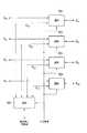
図1は、本発明の実施形態に係る積層型半導体装置の構成例を模式的に示した図である。
【0017】
本装置は、ベース基板(パッケージ基板等)10上に半導体集積回路チップ20、301及び302が積層されたものであり、それらの間にはバンプ(導電性接続部材)40が設けられている。半導体集積回路チップ20、301及び302には、それぞれ半導体基板を貫通する複数のスループラグ(図示せず)が設けられており、これらのスループラグ及びバンプ40を介して、各チップの回路間が電気的に接続されている。なお、以下の説明では便宜上、チップ20を特定チップ(所定のチップ)、チップ301及び302を非特定チップと呼ぶ場合もある。また、非特定チップの数は1以上、好ましくは2以上である。
【0018】
以下、図2、図3及び図4を参照して、半導体集積回路チップ20、301及び302の概略を説明する。
【0019】
図3(a)〜図3(c)は、半導体集積回路チップ(非特定チップ)30(図1の半導体集積回路チップ301或いは302に対応)のいくつかの態様を示した図である。
【0020】
図に示すように、チップ30は回路ブロック31a〜31dを含んで構成されている。図3(a)は、回路ブロック31a〜31dがいずれもロジック回路ブロックで構成されているチップ(ロジック系チップ)の例、図3(b)は、回路ブロック31a〜31dがいずれもメモリ回路ブロックで構成されているチップ(メモリ系チップ)の例、図3(c)は、回路ブロック31a及び31bがロジック回路ブロックで、回路ブロック31c及び31dがメモリ回路ブロックで構成されているチップ(混在チップ)の例である。なお、ロジック回路ブロックは、ロジック回路の組み合わせによって所定の動作を行うよう構成されたものであり、メモリ回路ブロックは、アドレス情報によって選択されるメモリセルが配列した構造を有するものである。
【0021】
図3(a)〜図3(c)に示した各非特定チップ30は、任意の組み合わせで積層可能である。すなわち、ロジック系チップのみ、メモリ系チップのみ、混在チップのみといったように、同種のチップのみを積層したものでもよいし、異種のチップを組み合わせて積層したものでもよい。
【0022】
1又は2以上の非特定チップ30にロジック回路ブロック及びメモリ回路ブロックの双方が含まれている場合、ロジック回路ブロックからなるグループとメモリ回路ブロックからなるグループとに分けられる。ロジック回路ブロックのグループに含まれる各回路ブロックは、通常は互いに異なった回路構成であり、互いに異なった回路動作が行われる。メモリ回路ブロックのグループに含まれる各回路ブロックは、互いに異なった回路構成であってもよいが、通常は互いに等価な回路構成(実質的に同一の回路構成)になっている。なお、例えばDRAMブロックとEEPROMブロックといったように、異種のメモリ回路ブロックが含まれている場合には、DRAMブロック及びEEPROMブロックそれぞれのグループ内において、各回路ブロックが互いに等価な回路構成になっている。
【0023】
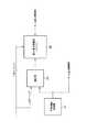
図2は、半導体集積回路チップ(特定チップ)20の内部構成例を示したブロック図である。
【0024】
半導体集積回路チップ20内には、不良情報記憶部21、置き換え回路部22及び、置き換え回路部22の制御等を行う制御部23が含まれている。
【0025】
不良情報記憶部21は、チップ301或いは302に不良回路ブロックが含まれている場合に、該不良回路ブロックを特定するための不良情報を記憶するものである。例えば、不良情報記憶部21には、不良回路ブロックのアドレス情報が記憶される。また、不良回路ブロックが存在しない場合には、その旨を記憶するようにしてもよい。
【0026】
不良情報記憶部21には、例えば不揮発性の記憶素子を用いることができる。この不揮発性の記憶素子には、電気的に書き込み可能なものを用いてもよいが、本実施形態では、外部からのレーザービームによって溶断されるヒューズを用いている。ヒューズ部は、レーザービームを照射することが可能な位置に配置されており、本例では、図1に示すように、チップ20がチップ301及び302とオーバーラップしない領域内にヒューズ部21aが配置されている。なお、ヒューズ部21aは、レーザービームを照射可能な位置に配置されていればよく、例えば特定チップ20を最上層に配置した場合には、特定チップ20表面の所望の位置にヒューズ部21aを配置することも可能である。
【0027】
置き換え回路部22は、チップ301或いは302に不良回路ブロックが含まれている場合に、不良回路ブロックを置き換えるために用いられる。ロジック回路ブロックの置き換え用としては、外部からプログラム可能なプログラマブル回路、例えばFPGA(Field Programmable Gate Array)が用いられる。チップ301或いは302に不良のロジック回路ブロックが含まれている場合には、置き換え回路部22には該不良のロジック回路ブロックと等価な回路が作製(プログラム)されている。チップ301或いは302に不良のロジック回路ブロックが含まれていない場合には、プログラムされない状態が維持されている。メモリ回路ブロック置き換え用の置き換え回路部22では、メモリ回路ブロックと等価な回路がチップ積層前に予め形成されている。
【0028】
図4は、半導体集積回路チップ(非特定チップ)30の内部構成例を示したブロック図である。
【0029】
回路ブロック31a〜31dは入出力制御部32に接続されており、入出力制御部32では、チップ20内の不良情報記憶部21からの不良情報に基づいて、回路ブロック31a〜31dとチップ20内の置き換え回路部22との間の入出力関係を制御する。すなわち、回路ブロック31a〜31dの中に不良回路ブロックが含まれている場合には、不良回路ブロックに入力すべき信号は入出力制御部32を介して置き換え回路部22に送られ、また、置き換え回路部22から入出力制御部32を介して送られてきた信号が不良回路ブロックから出力されるべき信号の代わりに出力信号として用いられる。
【0030】
図5は、図4に示した入出力制御部32について、その具体例を示したブロック図である。
【0031】
図5に示すように、入出力制御部32には、回路ブロック31aと回路ブロック31a外の回路との間に設けられた選択部32a、回路ブロック31bと回路ブロック31b外の回路との間に設けられた選択部32b、回路ブロック31cと回路ブロック31c外の回路との間に設けられた選択部32c、回路ブロック31dと回路ブロック31d外の回路との間に設けられた選択部32d、及び、選択部32a〜32dとチップ20内の置き換え回路部22との間に設けられた選択部32rが含まれている。各選択部32a、32b、32c、32d及び32rには、チップ20内の不良情報記憶部21からの不良情報が選択信号として入力している。
【0032】
例えば、回路ブロック31aが不良である場合を想定して説明する。この場合には、選択回路32aでは、不良情報記憶部21からの不良情報に基づき、回路ブロック31aに対する入出力信号Sa1を非選択状態にし、置き換え回路部22に対する入出力信号Sa2を選択状態にする。その結果、回路ブロック31aに入力すべき信号Sa3は、信号Sa2として選択部32rを介して置き換え回路部22に送られる。また、回路ブロック31aから本来出力されるべき信号の代わりに、置き換え回路部22から選択部32rを介して送られてきた信号Sa2が、出力信号Sa3として回路ブロック31a外の回路に供給される。回路ブロック31a以外の正常な回路ブロック31b、31c及び31dについては、それぞれ信号Sb1、Sc1及びSd1が選択される。なお、回路ブロック31a〜31dのいずれも不良でない場合には、選択部32a〜32dは信号Sa1〜Sd1を選択し、置き換え回路部22に対する信号の送受は行われない。
【0033】
なお、図5に示した入出力制御部の構成は、ロジック回路ブロック及びメモリ回路ブロックいずれについても、それらの入力部、出力部及び入出力部(例えばメモリブロックのI/O端子のように入力と出力が共通であるもの)に対して適用可能である。ただし、メモリ回路ブロック及びその置き換え回路に対するアドレス信号入力については、図5に示したような構成とは異なる構成を採用することも可能である。
【0034】
図6は、そのような構成を採用した場合の、チップ20内の構成例を示したブロック図である。
【0035】
本例では、回路ブロック(メモリ回路ブロック)31a〜31dのブロック選択信号として、アドレス信号の上位ビット(本例では2ビット)を用いている。アドレス信号は、非特定チップに入力してメモリ回路ブロックの選択及びメモリ回路ブロックに含まれるメモリセルの選択に用いられる他、特定チップ20にも入力している。そして、チップ20の不良情報記憶部21には、不良回路ブロックのアクセスに用いられるビット情報(本例では2ビット)が不良情報として記憶される。
【0036】
外部からアドレス信号が供給されると、その上位ビットは、図2に示した制御部23に含まれる選択部24に送られる。アドレス信号の上位ビットが不良情報記憶部21に記憶されている不良回路ブロックのアドレスと一致した場合、すなわち不良回路ブロックをアクセスするためのアドレス信号が送られてきた場合には、選択部24によって置き換え回路部22が選択される。置き換え回路部22にはアドレス信号の下位ビットが入力しているため、置き換え回路部22では指定されたアドレスに対応したメモリセルが選択され、選択されたメモリセルに対してデータの書き込みや読み出しが行われる。置き換え回路部22の入出力部は、図4に示した入出力制御部32に接続されており、データの送受は入出力制御部32を介して行われる。
【0037】
この場合、その一部の上位ビットをメモリ回路ブロックを選択する信号情報としたアドレス信号を特定チップ20にも供給するとともに、不良回路ブロックを選択するための信号情報を不良情報として記憶しておくことで、アドレス信号入力に対しては図5に示したような回路を設けないですむ。また、アドレス信号とは別にメモリ回路ブロックを選択するブロック選択信号が入力される場合についても、アドレス信号入力及びブロック選択信号入力に対して、図5に示したような回路を設けない構成を採用可能である。
【0038】
次に、本実施形態に係る積層型半導体装置の製造方法を、図7に示したフローチャートを参照して説明する。なお、本例では、積層型半導体装置にロジック回路ブロック及びメモリ回路ブロックの両方が含まれている場合を想定して説明を行う。
【0039】
まず、各半導体集積回路チップをベース基板上に積層する(S1)。続いて、チップが積層された状態でモジュール全体のテストを行う(S2)。次に、テスト結果に基づいて不良の有無を判断する(S3)。不良がない場合には、後述する最終テストへと移行する。不良がある場合には、不良情報記憶部21に不良情報を書き込む(S4)。次に、不良がロジック回路ブロックの不良であるか否かを判断する(S5)。ロジック回路ブロックの不良でない場合、すなわちメモリ回路ブロックの不良である場合には、後述する最終テストへと移行する。ロジック回路ブロックの不良である場合には、不良ロジック回路ブロックと等価な回路を置き換え回路部22に作製する。例えば、置き換え回路部22にFPGAを用いた場合には、不良ロジック回路ブロックと等価な回路をFPGAにプログラムすればよい(S6)。その後、最終テストを行い、モジュール全体の最終的な良否を判定する(S7)。
【0040】
以上のように、本実施形態によれば、所定のチップ(特定チップ)に、他のチップ(非特定チップ)の不良回路ブロックを特定するための情報を記憶する記憶部と、不良回路ブロックを置き換えるための置き換え回路部を設けている。そのため、チップを積層した状態でモジュール全体のテストを行い、不良回路ブロックが検出された場合には、置き換え回路部を用いることで不良回路ブロックを救済することができる。したがって、テストに費やされる時間や手間を低減することができるとともに、モジュール全体の歩留まりを向上させることができる。また、所定のチップに設けた置き換え回路部を他のチップで共用することができるため、置き換え用の回路を最小限に抑えることが可能となる。したがって、納期の遅延やコストの上昇を防止することが可能な優れた積層型半導体装置を得ることが可能である。
【0041】
以上、本発明の実施形態を説明したが、本発明は上記実施形態に限定されるものではなく、その趣旨を逸脱しない範囲内において種々変形して実施することが可能である。さらに、上記実施形態には種々の段階の発明が含まれており、開示された構成要件を適宜組み合わせることによって種々の発明が抽出され得る。例えば、開示された構成要件からいくつかの構成要件が削除されても、所定の効果が得られるものであれば発明として抽出され得る。
【0042】
【発明の効果】
本発明によれば、チップを積層した状態でテストが可能で、しかも歩留まりの低下や余分な回路の増大を防止することが可能な優れた積層型半導体装置を得ることができる。
【図面の簡単な説明】
【図1】本発明の実施形態に係る積層型半導体装置の構成例を模式的に示した図である。
【図2】本発明の実施形態に係り、半導体集積回路チップ(特定チップ)の内部構成例を示したブロック図である。
【図3】本発明の実施形態に係り、半導体集積回路チップ(非特定チップ)のいくつかの態様を示した図である。
【図4】本発明の実施形態に係り、半導体集積回路チップ(非特定チップ)の内部構成例を示したブロック図である。
【図5】図4に示した入出力制御部の具体例を示したブロック図である。
【図6】本発明の実施形態に係り、半導体集積回路チップ(特定チップ)の内部構成例を示したブロック図である。
【図7】本発明の実施形態に係る積層型半導体装置の製造方法を示したフローチャートである。
【符号の説明】
10…ベース基板
20、30、301、302…半導体集積回路チップ
21…不良情報記憶部
21a…ヒューズ部
22…置き換え回路部
23…制御部
24…選択部
31a〜31d…回路ブロック
32…入出力制御部
40…バンプ
32a〜32d、32r…選択部[0001]
BACKGROUND OF THE INVENTION
The present invention relates to a stacked semiconductor device in which a plurality of semiconductor integrated circuit chips are stackedand a manufacturing method thereof .
[0002]
[Prior art]
In response to a demand for downsizing electronic devices, a stacked semiconductor device (multi-chip device) in which a plurality of semiconductor integrated circuit chips (LSI chips) are stacked has been proposed.
[0003]
When manufacturing a stacked semiconductor device, a method is conceivable in which an operation test or the like is individually performed for each chip, and only normal chips are selected and stacked. However, performing a test on each chip leads to an increase in time and labor required for the test, causing problems such as an increase in cost and a delay in delivery time.
[0004]
For such a problem, a method of stacking chips without performing individual tests for each chip and testing the entire module after stacking is also conceivable. However, if there is even one defective chip among the stacked chips, the entire module will be defective. As a result, there arises a problem that the yield decreases and the cost increases. Although it is conceivable to provide a redundant circuit for each chip, it is wasteful to provide an extra circuit for each chip, which also leads to an increase in cost.
[0005]
Therefore, conventionally, it has been difficult to obtain a stacked semiconductor device that can be tested in a state where chips are stacked, and that can prevent a decrease in yield and an increase in extra circuits.
[0006]
As a known technique, Patent Document 1 discloses a technique in which one chip has a plurality of functional blocks and a defective block is replaced with another chip. Specifically, each functional block and a specular target chip are prepared in advance for each functional block, and the specular target chip is stacked on the defective functional block. However, it is necessary to perform a test in advance before stacking the mirror surface target chips, which leads to an increase in time and labor. In addition, a mirror surface target chip must be prepared for each functional block, which also increases time and labor.
[0007]
Japanese Patent Application Laid-Open No. 2004-228561 discloses a technique in which a stacked DRAM is configured by combining defective chips (partial chips) in which part of an address space does not function normally. However, it is necessary to test whether the chip is defective before stacking, leading to an increase in time and labor.
[0008]
Patent Document 3 discloses a configuration in which a redundant circuit is provided in each DRAM chip in a semiconductor device in which a plurality of DRAM chips are stacked. However, since a redundant circuit is provided for each chip, waste is increased, resulting in an increase in cost.
[0009]
[Patent Document 1]
Japanese Patent No. 2760188 Specification
[Patent Document 2]
JP 2000-349229 A
[Patent Document 3]
JP-A-5-283606 [0012]
[Problems to be solved by the invention]
As described above, a stacked semiconductor device in which a plurality of semiconductor integrated circuit chips are stacked has been proposed. Conventionally, a test can be performed in a state in which chips are stacked, and the yield is reduced and the number of extra circuits is increased. It has been difficult to obtain a stacked semiconductor device that can be prevented.
[0013]
An object of the present invention is to provide a stacked semiconductor deviceand a method formanufacturing the same that can solve the above-described conventional problems.
[0014]
[Means for Solving the Problems]
A stacked semiconductor device according to an aspect of the present invention is a stacked semiconductor device in which a predetermined semiconductor integrated circuit chip and at least one semiconductor integrated circuit chip other than the predetermined semiconductor integrated circuit chip are stacked. The at least one semiconductor integrated circuit chip includes a group of a plurality of circuit blocks, and the predetermined semiconductor integrated circuit chip has a defective circuit block when the defective circuit block is included in the group. It includes a storage unit for storing defect information for specifying a circuit block, and a replacement circuit unit for replacing the defective circuit block.
[0015]
DETAILED DESCRIPTION OF THE INVENTION
Embodiments of the present invention will be described below with reference to the drawings.
[0016]
FIG. 1 is a diagram schematically showing a configuration example of a stacked semiconductor device according to an embodiment of the present invention.
[0017]
In this apparatus, semiconductor integrated
[0018]
The outline of the semiconductor integrated
[0019]
FIGS. 3A to 3C are diagrams showing some aspects of the semiconductor integrated circuit chip (non-specific chip) 30 (corresponding to the semiconductor integrated
[0020]
As shown in the figure, the
[0021]
Each
[0022]
When one or more
[0023]
FIG. 2 is a block diagram illustrating an internal configuration example of the semiconductor integrated circuit chip (specific chip) 20.
[0024]
The semiconductor integrated
[0025]
The defect
[0026]
For example, a nonvolatile storage element can be used for the defect
[0027]
The
[0028]
FIG. 4 is a block diagram illustrating an internal configuration example of the semiconductor integrated circuit chip (non-specific chip) 30.
[0029]
The circuit blocks 31 a to 31 d are connected to the input /
[0030]
FIG. 5 is a block diagram showing a specific example of the input /
[0031]
As shown in FIG. 5, the input /
[0032]
For example, the case where the
[0033]
Note that the configuration of the input / output control unit shown in FIG. 5 is such that the input unit, the output unit, and the input / output unit (such as the I / O terminal of the memory block) are input to both the logic circuit block and the memory circuit block. And the output is common). However, for the address signal input to the memory circuit block and its replacement circuit, a configuration different from the configuration shown in FIG. 5 can be adopted.
[0034]
FIG. 6 is a block diagram showing a configuration example in the
[0035]
In this example, the upper bits (2 bits in this example) of the address signal are used as block selection signals for the circuit blocks (memory circuit blocks) 31a to 31d. The address signal is input to the non-specific chip and used to select the memory circuit block and the memory cell included in the memory circuit block, and is also input to the
[0036]
When an address signal is supplied from the outside, the upper bits are sent to the
[0037]
In this case, an address signal in which some of the upper bits are signal information for selecting a memory circuit block is supplied to the
[0038]
Next, a method for manufacturing the stacked semiconductor device according to this embodiment will be described with reference to the flowchart shown in FIG. In this example, the description is given assuming that the stacked semiconductor device includes both a logic circuit block and a memory circuit block.
[0039]
First, each semiconductor integrated circuit chip is stacked on a base substrate (S1). Subsequently, the entire module is tested with the chips stacked (S2). Next, it is determined whether there is a defect based on the test result (S3). If there is no defect, the process proceeds to the final test described later. If there is a defect, the defect information is written in the defect information storage unit 21 (S4). Next, it is determined whether or not the failure is a failure of the logic circuit block (S5). If the logic circuit block is not defective, that is, if the memory circuit block is defective, the process proceeds to the final test described later. If the logic circuit block is defective, a circuit equivalent to the defective logic circuit block is formed in the
[0040]
As described above, according to the present embodiment, a predetermined chip (specific chip) includes a storage unit that stores information for specifying a defective circuit block of another chip (non-specific chip), and a defective circuit block. A replacement circuit unit for replacement is provided. Therefore, when the entire module is tested in a state where chips are stacked and a defective circuit block is detected, the defective circuit block can be relieved by using the replacement circuit unit. Therefore, it is possible to reduce the time and labor required for the test and improve the yield of the entire module. Further, since the replacement circuit portion provided in a predetermined chip can be shared by other chips, the replacement circuit can be minimized. Therefore, it is possible to obtain an excellent stacked semiconductor device capable of preventing a delay in delivery date and an increase in cost.
[0041]
Although the embodiments of the present invention have been described above, the present invention is not limited to the above-described embodiments, and various modifications can be made without departing from the spirit of the present invention. Furthermore, the above embodiments include inventions at various stages, and various inventions can be extracted by appropriately combining the disclosed constituent elements. For example, even if several constituent requirements are deleted from the disclosed constituent requirements, the invention can be extracted as an invention as long as a predetermined effect can be obtained.
[0042]
【The invention's effect】
According to the present invention, it is possible to obtain an excellent stacked semiconductor device that can be tested in a state where chips are stacked, and that can prevent a decrease in yield and an increase in extra circuits.
[Brief description of the drawings]
FIG. 1 is a diagram schematically showing a configuration example of a stacked semiconductor device according to an embodiment of the present invention.
FIG. 2 is a block diagram showing an internal configuration example of a semiconductor integrated circuit chip (specific chip) according to the embodiment of the present invention.
FIG. 3 is a diagram showing some aspects of a semiconductor integrated circuit chip (non-specific chip) according to the embodiment of the present invention.
FIG. 4 is a block diagram showing an internal configuration example of a semiconductor integrated circuit chip (non-specific chip) according to the embodiment of the present invention.
5 is a block diagram showing a specific example of the input / output control unit shown in FIG. 4. FIG.
FIG. 6 is a block diagram showing an internal configuration example of a semiconductor integrated circuit chip (specific chip) according to the embodiment of the present invention.
FIG. 7 is a flowchart showing a method for manufacturing a stacked semiconductor device according to an embodiment of the present invention.
[Explanation of symbols]
10 ...
Claims (13)
Translated fromJapanese前記少なくとも2以上の半導体集積回路チップは、複数の回路ブロックからなるグループを含み、
前記所定の半導体集積回路チップは、前記グループのなかに不良の回路ブロックが含まれている場合に該不良の回路ブロックを特定するための不良情報を記憶する記憶部と、前記記憶部に記憶された不良情報に基づき該不良情報により特定される不良の回路ブロックを置き換えるための置き換え回路部と、を含む
ことを特徴とする積層型半導体装置。A stacked semiconductor device in which a predetermined semiconductor integrated circuit chip and at least two or more semiconductor integrated circuit chips other than the predetermined semiconductor integrated circuit chip are stacked,
The at least two or more semiconductor integrated circuit chips include a group consisting of a plurality of circuit blocks,
The predetermined semiconductor integrated circuit chip is stored in the storage unit for storing defect information for specifying the defective circuit block when the defective circuit block is included in the group, and thestorage unit. And a replacement circuit unit for replacinga defective circuit blockspecified by the defect information based on the defect information .
前記少なくとも1以上の半導体集積回路チップは、複数の回路ブロックからなるグループを含み、
前記所定の半導体集積回路チップは、前記グループのなかに不良の回路ブロックが含まれている場合に該不良の回路ブロックを特定するための不良情報を記憶する記憶部と、前記記憶部に記憶された不良情報に基づき該不良情報により特定される不良の回路ブロックを置き換えるための置き換え回路部と、を含み、
前記記憶部はヒューズ部を含み、該ヒューズ部は外部からエネルギービームを照射可能な所定位置に配置され、
前記所定位置は、前記所定の半導体集積回路チップが前記少なくとも1以上の半導体集積回路チップとオーバーラップしない領域に含まれる
ことを特徴とする積層型半導体装置。A stacked semiconductor device in which a predetermined semiconductor integrated circuit chip and at least one semiconductor integrated circuit chip other than the predetermined semiconductor integrated circuit chip are stacked,
The at least one semiconductor integrated circuit chip includes a group of a plurality of circuit blocks;
The predetermined semiconductor integrated circuit chip is stored in the storage unit for storing defect information for specifying the defective circuit block when the defective circuit block is included in the group, and thestorage unit. A replacement circuit unit for replacinga defective circuit blockspecified by the defect information based on the defect information ,
The storage unit includes a fuse unit, and the fuse unit is disposed at a predetermined position where an energy beam can be irradiated from the outside.
The predetermined position is included in a region where the predetermined semiconductor integrated circuit chip does not overlap with the at least one semiconductor integrated circuit chip.
ことを特徴とする請求項1又は2に記載の積層型半導体装置。The stacked semiconductor device according to claim 1, wherein the circuit block included in the group is a logic circuit block.
ことを特徴とする請求項3に記載の積層型半導体装置。The stacked semiconductor device according to claim 3, wherein the replacement circuit section includes a circuit equivalent to the defective circuit block.
ことを特徴とする請求項3に記載の積層型半導体装置。The stacked semiconductor device according to claim 3, wherein the replacement circuit unit is capable of forming an equivalent circuit for each of the circuit blocks included in the group.
ことを特徴とする請求項1又は2に記載の積層型半導体装置。The stacked semiconductor device according to claim 1, wherein the circuit block included in the group is a memory circuit block.
ことを特徴とする請求項6に記載の積層型半導体装置。The stacked semiconductor device according to claim 6, wherein the circuit blocks included in the group have circuits equivalent to each other.
ことを特徴とする請求項7に記載の積層型半導体装置。The stacked semiconductor device according to claim 7, wherein the replacement circuit unit includes a circuit equivalent to a circuit block included in the group.
ことを特徴とする請求項6に記載の積層型半導体装置。The predetermined semiconductor integrated circuit chip further includes a selection unit that selects the replacement circuit unit based on defect information from the storage unit and information for accessing the defective circuit block. Item 7. The stacked semiconductor device according to Item 6.
ことを特徴とする請求項1に記載の積層型半導体装置。The at least two or more semiconductor integrated circuit chips further include an input / output control unit that controls an input / output relationship between a circuit block included in the group and the replacement circuit unit based on defect information from the storage unit. The stacked semiconductor device according to claim 1, further comprising:
ことを特徴とする請求項2に記載の積層型半導体装置。The at least one semiconductor integrated circuit chip further includes an input / output control unit that controls an input / output relationship between a circuit block included in the group and the replacement circuit unit based on defect information from the storage unit. The stacked semiconductor device according to claim 2, further comprising:
前記少なくとも1以上の半導体集積回路チップは、複数の回路ブロックからなるグループを含み、
前記所定の半導体集積回路チップは、前記グループのなかに不良の回路ブロックが含まれている場合に該不良の回路ブロックを特定するための不良情報を記憶する記憶部と、前記記憶部に記憶された不良情報に基づき該不良情報により特定される不良の回路ブロックを置き換えるための置き換え回路部と、を含み、
前記所定の半導体集積回路チップと前記少なくとも1以上の半導体集積回路チップを積層する工程と、
前記所定の半導体集積回路チップと前記少なくとも1以上の半導体集積回路チップが積層された状態で積層されたモジュールのテストを行う工程と、
前記テスト結果に基づいて不良の回路ブロックの有無を判断する工程と、
不良の回路ブロックがあると判断された場合に、該不良の回路ブロックを特定するための不良情報を前記記憶部に記憶し、且つ不良の回路ブロックを前記置き換え回路部で置き換える工程と、
を備えたことを特徴とする積層型半導体装置の製造方法。A method of manufacturing a stacked semiconductor device in which a predetermined semiconductor integrated circuit chip and at least one semiconductor integrated circuit chip other than the predetermined semiconductor integrated circuit chip are stacked,
The at least one semiconductor integrated circuit chip includes a group of a plurality of circuit blocks;
The predetermined semiconductor integrated circuit chip is stored in the storage unit for storing defect information for specifying the defective circuit block when the defective circuit block is included in the group, and thestorage unit. A replacement circuit unit for replacinga defective circuit blockspecified by the defect information based on the defect information ,
Laminating the predetermined semiconductor integrated circuit chip and the at least one semiconductor integrated circuit chip;
Testing a module in which the predetermined semiconductor integrated circuit chip and the at least one semiconductor integrated circuit chip are stacked; and
Determining the presence or absence of defective circuit blocks based on the test results;
When it is determined that there is a defective circuit block, storing defect information for specifying the defective circuit block in the storage unit, and replacing the defective circuit block with the replacement circuit unit;
A method for manufacturing a stacked semiconductor device, comprising:
前記所定位置は、前記所定の半導体集積回路チップが前記少なくとも1以上の半導体集積回路チップとオーバーラップしない領域に含まれる
ことを特徴とする請求項12に記載の積層型半導体装置の製造方法。The storage unit includes a fuse unit, and the fuse unit is disposed at a predetermined position where an energy beam can be irradiated from the outside.
The method of manufacturing a stacked semiconductor device according to claim 12, wherein the predetermined position is included in a region where the predetermined semiconductor integrated circuit chip does not overlap with the at least one semiconductor integrated circuit chip.
Priority Applications (4)
| Application Number | Priority Date | Filing Date | Title |
|---|---|---|---|
| JP2002286515AJP3828473B2 (en) | 2002-09-30 | 2002-09-30 | Multilayer semiconductor device and manufacturing method thereof |
| TW092126387ATWI230395B (en) | 2002-09-30 | 2003-09-24 | Lamination type semiconductor device |
| CNA031600840ACN1490874A (en) | 2002-09-30 | 2003-09-26 | Stacked Semiconductor Devices |
| US10/673,192US6812557B2 (en) | 2002-09-30 | 2003-09-30 | Stacked type semiconductor device |
Applications Claiming Priority (1)
| Application Number | Priority Date | Filing Date | Title |
|---|---|---|---|
| JP2002286515AJP3828473B2 (en) | 2002-09-30 | 2002-09-30 | Multilayer semiconductor device and manufacturing method thereof |
Publications (2)
| Publication Number | Publication Date |
|---|---|
| JP2004128014A JP2004128014A (en) | 2004-04-22 |
| JP3828473B2true JP3828473B2 (en) | 2006-10-04 |
Family
ID=32279546
Family Applications (1)
| Application Number | Title | Priority Date | Filing Date |
|---|---|---|---|
| JP2002286515AExpired - Fee RelatedJP3828473B2 (en) | 2002-09-30 | 2002-09-30 | Multilayer semiconductor device and manufacturing method thereof |
Country Status (4)
| Country | Link |
|---|---|
| US (1) | US6812557B2 (en) |
| JP (1) | JP3828473B2 (en) |
| CN (1) | CN1490874A (en) |
| TW (1) | TWI230395B (en) |
Families Citing this family (20)
| Publication number | Priority date | Publication date | Assignee | Title |
|---|---|---|---|---|
| US6780696B1 (en)* | 2000-09-12 | 2004-08-24 | Alien Technology Corporation | Method and apparatus for self-assembly of functional blocks on a substrate facilitated by electrode pairs |
| US7056810B2 (en)* | 2002-12-18 | 2006-06-06 | Semiconductor Energy Laboratory Co., Ltd. | Method for manufacturing semiconductor apparatus, and semiconductor apparatus and electric appliance |
| US7287177B2 (en)* | 2003-12-04 | 2007-10-23 | International Business Machines Corporation | Digital reliability monitor having autonomic repair and notification capability |
| US20050144524A1 (en)* | 2003-12-04 | 2005-06-30 | International Business Machines Corporation | Digital reliability monitor having autonomic repair and notification capability |
| US7078792B2 (en)* | 2004-04-30 | 2006-07-18 | Atmel Corporation | Universal interconnect die |
| US8074082B2 (en)* | 2004-10-08 | 2011-12-06 | Aprolase Development Co., Llc | Anti-tamper module |
| EP1840964A1 (en)* | 2006-03-31 | 2007-10-03 | Irvine Sensors Corp. | Semiconductor device with protected access |
| DE102007007566B4 (en)* | 2007-02-15 | 2012-08-23 | Qimonda Ag | Semiconductor device system, memory module, and method of operating a semiconductor device system |
| TWI470762B (en)* | 2007-07-27 | 2015-01-21 | 尼康股份有限公司 | Laminated semiconductor device |
| US8679861B2 (en)* | 2007-11-29 | 2014-03-25 | International Business Machines Corporation | Semiconductor chip repair by stacking of a base semiconductor chip and a repair semiconductor chip |
| US8597960B2 (en)* | 2008-03-04 | 2013-12-03 | International Business Machines Corporation | Semiconductor chip stacking for redundancy and yield improvement |
| US8384417B2 (en) | 2008-09-10 | 2013-02-26 | Qualcomm Incorporated | Systems and methods utilizing redundancy in semiconductor chip interconnects |
| JP2010080801A (en)* | 2008-09-29 | 2010-04-08 | Hitachi Ltd | Semiconductor device |
| KR101013565B1 (en) | 2009-06-29 | 2011-02-14 | 주식회사 하이닉스반도체 | Laminated Semiconductor Packages |
| US8063654B2 (en)* | 2009-07-17 | 2011-11-22 | Xilinx, Inc. | Apparatus and method for testing of stacked die structure |
| JP2014071932A (en)* | 2012-10-01 | 2014-04-21 | Toppan Printing Co Ltd | Multi-chip memory module |
| GB2511087A (en)* | 2013-02-22 | 2014-08-27 | Ibm | System for electrical testing and manufacturing a 3D chip stack and method |
| US9170296B2 (en) | 2013-08-06 | 2015-10-27 | Globalfoundries U.S.2 Llc | Semiconductor device defect monitoring using a plurality of temperature sensing devices in an adjacent semiconductor device |
| WO2017126014A1 (en)* | 2016-01-18 | 2017-07-27 | ウルトラメモリ株式会社 | Layered semiconductor device, and production method therefor |
| CN114402297A (en)* | 2019-09-16 | 2022-04-26 | 赛灵思公司 | Redundancy scheme for multi-chip stacking apparatus |
Family Cites Families (15)
| Publication number | Priority date | Publication date | Assignee | Title |
|---|---|---|---|---|
| GB1487945A (en)* | 1974-11-20 | 1977-10-05 | Ibm | Semiconductor integrated circuit devices |
| JPS61111561A (en)* | 1984-10-05 | 1986-05-29 | Fujitsu Ltd | semiconductor equipment |
| US4954875A (en)* | 1986-07-17 | 1990-09-04 | Laser Dynamics, Inc. | Semiconductor wafer array with electrically conductive compliant material |
| JP2760188B2 (en) | 1991-11-08 | 1998-05-28 | 日本電気株式会社 | Semiconductor integrated circuit |
| JPH05283606A (en) | 1992-04-03 | 1993-10-29 | Hitachi Ltd | Semiconductor device |
| US5426072A (en)* | 1993-01-21 | 1995-06-20 | Hughes Aircraft Company | Process of manufacturing a three dimensional integrated circuit from stacked SOI wafers using a temporary silicon substrate |
| US5698895A (en)* | 1994-06-23 | 1997-12-16 | Cubic Memory, Inc. | Silicon segment programming method and apparatus |
| US6486528B1 (en)* | 1994-06-23 | 2002-11-26 | Vertical Circuits, Inc. | Silicon segment programming apparatus and three terminal fuse configuration |
| JP2001102479A (en) | 1999-09-27 | 2001-04-13 | Toshiba Corp | Semiconductor integrated circuit device and method of manufacturing the same |
| JP3249805B2 (en) | 2000-01-01 | 2002-01-21 | 株式会社日立製作所 | Semiconductor device |
| JP3779524B2 (en) | 2000-04-20 | 2006-05-31 | 株式会社東芝 | Multi-chip semiconductor device and memory card |
| US6353264B1 (en)* | 2000-07-18 | 2002-03-05 | Trw Inc. | Pseudomonolithic wafer scale module |
| JP2002110865A (en) | 2000-09-27 | 2002-04-12 | Toshiba Corp | Circuit device |
| JP2002305286A (en)* | 2001-02-01 | 2002-10-18 | Mitsubishi Electric Corp | Semiconductor modules and electronic components |
| US6737738B2 (en)* | 2002-07-16 | 2004-05-18 | Kingston Technology Corporation | Multi-level package for a memory module |
- 2002
- 2002-09-30JPJP2002286515Apatent/JP3828473B2/ennot_activeExpired - Fee Related
- 2003
- 2003-09-24TWTW092126387Apatent/TWI230395B/ennot_activeIP Right Cessation
- 2003-09-26CNCNA031600840Apatent/CN1490874A/enactivePending
- 2003-09-30USUS10/673,192patent/US6812557B2/ennot_activeExpired - Lifetime
Also Published As
| Publication number | Publication date |
|---|---|
| TW200411721A (en) | 2004-07-01 |
| US20040129939A1 (en) | 2004-07-08 |
| CN1490874A (en) | 2004-04-21 |
| US6812557B2 (en) | 2004-11-02 |
| TWI230395B (en) | 2005-04-01 |
| JP2004128014A (en) | 2004-04-22 |
Similar Documents
| Publication | Publication Date | Title |
|---|---|---|
| JP3828473B2 (en) | Multilayer semiconductor device and manufacturing method thereof | |
| US8040745B2 (en) | Stacked memory and fuse chip | |
| US6624506B2 (en) | Multichip semiconductor device and memory card | |
| TW564526B (en) | Laminated type semiconductor device | |
| US6649931B2 (en) | Semiconductor wafer, semiconductor chip, semiconductor device and method for manufacturing semiconductor device | |
| TWI503834B (en) | Methods and system for storage of repair data | |
| US7779311B2 (en) | Testing and recovery in a multilayer device | |
| EP3472708B1 (en) | Shared error detection and correction memory | |
| JPH11219598A (en) | Semiconductor storage device | |
| JP5481444B2 (en) | Semiconductor device | |
| US7706198B2 (en) | Multi-chip and repairing method based on remaining redundancy cells | |
| US8853847B2 (en) | Stacked chip module with integrated circuit chips having integratable and reconfigurable built-in self-maintenance blocks | |
| US7404117B2 (en) | Component testing and recovery | |
| US8659018B2 (en) | Semiconductor device and integrated semiconductor device | |
| JP5247827B2 (en) | Memory circuit stack manufacturing method, memory circuit addressing method, and corresponding stack and apparatus | |
| KR100900599B1 (en) | Semiconductor memory device and method of testing the same | |
| KR20190069782A (en) | Stacked Memory Apparatus Using Base Die Spare Cell and Repair Method Thereof | |
| JP2003059286A (en) | Semiconductor device | |
| JPH10289595A (en) | Semiconductor memory device and method of manufacturing the same | |
| JP5559616B2 (en) | Semiconductor memory device | |
| US6295236B1 (en) | Semiconductor memory of the random access type with a bus system organized in two planes | |
| JP3198546B2 (en) | Semiconductor device having redundant memory cells | |
| US20250037785A1 (en) | Stacked memory and manufacturing method therefor | |
| JPH11177059A (en) | Semiconductor memory device | |
| US20100135153A1 (en) | Redundant signal transmission |
Legal Events
| Date | Code | Title | Description |
|---|---|---|---|
| A977 | Report on retrieval | Free format text:JAPANESE INTERMEDIATE CODE: A971007 Effective date:20041020 | |
| A131 | Notification of reasons for refusal | Free format text:JAPANESE INTERMEDIATE CODE: A131 Effective date:20041102 | |
| A521 | Request for written amendment filed | Free format text:JAPANESE INTERMEDIATE CODE: A523 Effective date:20050104 | |
| A131 | Notification of reasons for refusal | Free format text:JAPANESE INTERMEDIATE CODE: A131 Effective date:20051004 | |
| A521 | Request for written amendment filed | Free format text:JAPANESE INTERMEDIATE CODE: A523 Effective date:20051019 | |
| TRDD | Decision of grant or rejection written | ||
| A01 | Written decision to grant a patent or to grant a registration (utility model) | Free format text:JAPANESE INTERMEDIATE CODE: A01 Effective date:20060704 | |
| A61 | First payment of annual fees (during grant procedure) | Free format text:JAPANESE INTERMEDIATE CODE: A61 Effective date:20060706 | |
| R151 | Written notification of patent or utility model registration | Ref document number:3828473 Country of ref document:JP Free format text:JAPANESE INTERMEDIATE CODE: R151 | |
| FPAY | Renewal fee payment (event date is renewal date of database) | Free format text:PAYMENT UNTIL: 20090714 Year of fee payment:3 | |
| FPAY | Renewal fee payment (event date is renewal date of database) | Free format text:PAYMENT UNTIL: 20100714 Year of fee payment:4 | |
| FPAY | Renewal fee payment (event date is renewal date of database) | Free format text:PAYMENT UNTIL: 20110714 Year of fee payment:5 | |
| FPAY | Renewal fee payment (event date is renewal date of database) | Free format text:PAYMENT UNTIL: 20120714 Year of fee payment:6 | |
| FPAY | Renewal fee payment (event date is renewal date of database) | Free format text:PAYMENT UNTIL: 20130714 Year of fee payment:7 | |
| S111 | Request for change of ownership or part of ownership | Free format text:JAPANESE INTERMEDIATE CODE: R313111 | |
| R350 | Written notification of registration of transfer | Free format text:JAPANESE INTERMEDIATE CODE: R350 | |
| LAPS | Cancellation because of no payment of annual fees |