JP3822976B2 - Semiconductor device and manufacturing method thereof - Google Patents
Semiconductor device and manufacturing method thereofInfo
- Publication number
- JP3822976B2 JP3822976B2JP05527298AJP5527298AJP3822976B2JP 3822976 B2JP3822976 B2JP 3822976B2JP 05527298 AJP05527298 AJP 05527298AJP 5527298 AJP5527298 AJP 5527298AJP 3822976 B2JP3822976 B2JP 3822976B2
- Authority
- JP
- Japan
- Prior art keywords
- semiconductor layer
- cleavage
- semiconductor
- substrate
- semiconductor device
- Prior art date
- Legal status (The legal status is an assumption and is not a legal conclusion. Google has not performed a legal analysis and makes no representation as to the accuracy of the status listed.)
- Expired - Lifetime
Links
- 239000004065semiconductorSubstances0.000titleclaimsdescription308
- 238000004519manufacturing processMethods0.000titleclaimsdescription37
- 238000003776cleavage reactionMethods0.000claimsdescription194
- 230000007017scissionEffects0.000claimsdescription194
- 239000000758substrateSubstances0.000claimsdescription104
- 238000000034methodMethods0.000claimsdescription41
- 150000001875compoundsChemical class0.000claimsdescription19
- 150000004767nitridesChemical class0.000claimsdescription18
- 238000001312dry etchingMethods0.000claimsdescription13
- 238000010030laminatingMethods0.000claimsdescription8
- 229910052594sapphireInorganic materials0.000description57
- 239000010980sapphireSubstances0.000description57
- 229910002704AlGaNInorganic materials0.000description26
- 238000005253claddingMethods0.000description21
- 238000005530etchingMethods0.000description18
- 230000003287optical effectEffects0.000description14
- 230000015572biosynthetic processEffects0.000description5
- 238000007796conventional methodMethods0.000description4
- 238000003754machiningMethods0.000description4
- 239000000463materialSubstances0.000description4
- 238000001020plasma etchingMethods0.000description4
- 230000035882stressEffects0.000description4
- 230000005669field effectEffects0.000description3
- 238000000992sputter etchingMethods0.000description3
- IJGRMHOSHXDMSA-UHFFFAOYSA-NAtomic nitrogenChemical compoundN#NIJGRMHOSHXDMSA-UHFFFAOYSA-N0.000description2
- 229910052782aluminiumInorganic materials0.000description2
- 238000005336crackingMethods0.000description2
- 239000013078crystalSubstances0.000description2
- 230000007423decreaseEffects0.000description2
- 230000000694effectsEffects0.000description2
- 229910052733galliumInorganic materials0.000description2
- 230000001771impaired effectEffects0.000description2
- 229910052738indiumInorganic materials0.000description2
- -1GaNChemical compound0.000description1
- GYHNNYVSQQEPJS-UHFFFAOYSA-NGalliumChemical compound[Ga]GYHNNYVSQQEPJS-UHFFFAOYSA-N0.000description1
- 229910004298SiO 2Inorganic materials0.000description1
- XAGFODPZIPBFFR-UHFFFAOYSA-NaluminiumChemical compound[Al]XAGFODPZIPBFFR-UHFFFAOYSA-N0.000description1
- 229910052785arsenicInorganic materials0.000description1
- 229910052796boronInorganic materials0.000description1
- 238000005229chemical vapour depositionMethods0.000description1
- 239000011248coating agentSubstances0.000description1
- 238000000576coating methodMethods0.000description1
- 229910052681coesiteInorganic materials0.000description1
- 229910052906cristobaliteInorganic materials0.000description1
- 238000009826distributionMethods0.000description1
- 230000005684electric fieldEffects0.000description1
- 238000000407epitaxyMethods0.000description1
- 230000002349favourable effectEffects0.000description1
- 229910052737goldInorganic materials0.000description1
- 229910021478group 5 elementInorganic materials0.000description1
- APFVFJFRJDLVQX-UHFFFAOYSA-Nindium atomChemical compound[In]APFVFJFRJDLVQX-UHFFFAOYSA-N0.000description1
- 238000001459lithographyMethods0.000description1
- 229910052751metalInorganic materials0.000description1
- 239000002184metalSubstances0.000description1
- 238000012986modificationMethods0.000description1
- 230000004048modificationEffects0.000description1
- 229910052759nickelInorganic materials0.000description1
- 229910052757nitrogenInorganic materials0.000description1
- 230000005693optoelectronicsEffects0.000description1
- 238000000059patterningMethods0.000description1
- 229910052698phosphorusInorganic materials0.000description1
- 239000000377silicon dioxideSubstances0.000description1
- VYPSYNLAJGMNEJ-UHFFFAOYSA-Nsilicon dioxideInorganic materialsO=[Si]=OVYPSYNLAJGMNEJ-UHFFFAOYSA-N0.000description1
- 229910052682stishoviteInorganic materials0.000description1
- 230000008646thermal stressEffects0.000description1
- 230000007704transitionEffects0.000description1
- 229910052905tridymiteInorganic materials0.000description1
- 229910052720vanadiumInorganic materials0.000description1
- 238000001039wet etchingMethods0.000description1
- 229910052984zinc sulfideInorganic materials0.000description1
Images


Classifications
- H—ELECTRICITY
- H10—SEMICONDUCTOR DEVICES; ELECTRIC SOLID-STATE DEVICES NOT OTHERWISE PROVIDED FOR
- H10D—INORGANIC ELECTRIC SEMICONDUCTOR DEVICES
- H10D62/00—Semiconductor bodies, or regions thereof, of devices having potential barriers
- H10D62/40—Crystalline structures
- H10D62/405—Orientations of crystalline planes
- H—ELECTRICITY
- H01—ELECTRIC ELEMENTS
- H01S—DEVICES USING THE PROCESS OF LIGHT AMPLIFICATION BY STIMULATED EMISSION OF RADIATION [LASER] TO AMPLIFY OR GENERATE LIGHT; DEVICES USING STIMULATED EMISSION OF ELECTROMAGNETIC RADIATION IN WAVE RANGES OTHER THAN OPTICAL
- H01S5/00—Semiconductor lasers
- H01S5/02—Structural details or components not essential to laser action
- H01S5/0201—Separation of the wafer into individual elements, e.g. by dicing, cleaving, etching or directly during growth
- H01S5/0202—Cleaving
- H—ELECTRICITY
- H01—ELECTRIC ELEMENTS
- H01S—DEVICES USING THE PROCESS OF LIGHT AMPLIFICATION BY STIMULATED EMISSION OF RADIATION [LASER] TO AMPLIFY OR GENERATE LIGHT; DEVICES USING STIMULATED EMISSION OF ELECTROMAGNETIC RADIATION IN WAVE RANGES OTHER THAN OPTICAL
- H01S5/00—Semiconductor lasers
- H01S5/02—Structural details or components not essential to laser action
- H01S5/0206—Substrates, e.g. growth, shape, material, removal or bonding
- H01S5/0213—Sapphire, quartz or diamond based substrates
- H—ELECTRICITY
- H01—ELECTRIC ELEMENTS
- H01S—DEVICES USING THE PROCESS OF LIGHT AMPLIFICATION BY STIMULATED EMISSION OF RADIATION [LASER] TO AMPLIFY OR GENERATE LIGHT; DEVICES USING STIMULATED EMISSION OF ELECTROMAGNETIC RADIATION IN WAVE RANGES OTHER THAN OPTICAL
- H01S5/00—Semiconductor lasers
- H01S5/30—Structure or shape of the active region; Materials used for the active region
- H01S5/32—Structure or shape of the active region; Materials used for the active region comprising PN junctions, e.g. hetero- or double- heterostructures
- H01S5/323—Structure or shape of the active region; Materials used for the active region comprising PN junctions, e.g. hetero- or double- heterostructures in AIIIBV compounds, e.g. AlGaAs-laser, InP-based laser
- H01S5/32308—Structure or shape of the active region; Materials used for the active region comprising PN junctions, e.g. hetero- or double- heterostructures in AIIIBV compounds, e.g. AlGaAs-laser, InP-based laser emitting light at a wavelength less than 900 nm
- H01S5/32341—Structure or shape of the active region; Materials used for the active region comprising PN junctions, e.g. hetero- or double- heterostructures in AIIIBV compounds, e.g. AlGaAs-laser, InP-based laser emitting light at a wavelength less than 900 nm blue laser based on GaN or GaP
- H—ELECTRICITY
- H10—SEMICONDUCTOR DEVICES; ELECTRIC SOLID-STATE DEVICES NOT OTHERWISE PROVIDED FOR
- H10H—INORGANIC LIGHT-EMITTING SEMICONDUCTOR DEVICES HAVING POTENTIAL BARRIERS
- H10H20/00—Individual inorganic light-emitting semiconductor devices having potential barriers, e.g. light-emitting diodes [LED]
- H10H20/01—Manufacture or treatment
- H10H20/011—Manufacture or treatment of bodies, e.g. forming semiconductor layers
- H10H20/013—Manufacture or treatment of bodies, e.g. forming semiconductor layers having light-emitting regions comprising only Group III-V materials
- H10H20/0133—Manufacture or treatment of bodies, e.g. forming semiconductor layers having light-emitting regions comprising only Group III-V materials with a substrate not being Group III-V materials
- H10H20/01335—Manufacture or treatment of bodies, e.g. forming semiconductor layers having light-emitting regions comprising only Group III-V materials with a substrate not being Group III-V materials the light-emitting regions comprising nitride materials
Landscapes
- Physics & Mathematics (AREA)
- Condensed Matter Physics & Semiconductors (AREA)
- General Physics & Mathematics (AREA)
- Electromagnetism (AREA)
- Optics & Photonics (AREA)
- Semiconductor Lasers (AREA)
- Dicing (AREA)
- Led Devices (AREA)
Description
Translated fromJapanese【0001】
【発明の属する技術分野】
この発明は、半導体装置およびその製造方法に関し、特に、劈開により共振器端面を形成するようにした半導体レーザのような半導体装置に適用して好適なものである。
【0002】
【従来の技術】
ガリウム(Ga)、アルミニウム(Al)、インジウム(In)などのIII族元素と窒素(N)のV族元素とからなる窒化物系III−V族化合物半導体、例えば、GaN、AlGaN、GaInNなどは直接遷移型半導体であり、かつ、AlGaInAsやAlGaInPなど、既に実用化されている半導体レーザに用いられている半導体よりバンドギャップが大きいため、発光波長が400nm帯の短波長半導体レーザや、紫外乃至緑色で発光可能な発光ダイオード(LED)などの半導体発光素子など、高集積、高密度の光ディスク再生装置に用いられる光源やフルカラー表示素子に用いられる光素子などへの広い応用が期待されている。また、この窒化物系III−V族化合物半導体は、高電界における飽和電子速度が大きいことなどから高出力、高周波の電界効果トランジスタ(FET)など電子走行素子の材料としても注目されている。
【0003】
この窒化物系III−V族化合物半導体を用いた半導体レーザ、発光ダイオード、FETなどは、例えばサファイア(Al2O3)基板などの基板上に窒化物系III−V族化合物半導体をエピタキシャル成長させることにより製造される。
【0004】
ところで、一般に、半導体レーザにおいては、共振器端面を形成する必要がある。AlGaInAs系、AlGaInP系またはInP系の半導体レーザにおいては、基板やその上に成長される半導体層が劈開性を有しており、その劈開面を半導体レーザの共振器端面とする場合が多い。
【0005】
一方、窒化物系III−V族化合物半導体は、その結晶構造が六方晶系のウルツァイト構造であるという性質上、一般に、安定な劈開面を得ることが難しい。また、この窒化物系III−V族化合物半導体を用いた半導体レーザは、上述のようにサファイア基板上に窒化物系III−V族化合物半導体を成長させることにより製造される場合が多く、サファイア基板が劈開性を有していないため、劈開面を共振器端面とする半導体レーザの形成が難しかった。
【0006】
ここで、例えば特開平8−222807号公報および特開平9−172223号公報には、サファイア基板およびその上に積層されたIII−V族化合物半導体からなる半導体層を劈開することにより共振器端面を形成するようにした、GaN系半導体レーザの製造方法が開示されている。
【0007】
すなわち、この従来のGaN系半導体レーザの製造方法においては、図8に示すように、c面のサファイア基板101上に、有機金属化学気相成長(MOCVD)法により、GaNバッファ層102、n型GaNコンタクト層103、n型AlGaNクラッド層104、GaN/GaInN多重量子井戸構造の活性層105、p型AlGaNクラッド層106およびp型GaNコンタクト層107を順次成長させる。
【0008】
次に、p型GaNコンタクト層107上に所定のストライプ形状のレジストパターン(図示せず)を形成した後、このレジストパターンをマスクとして反応性イオンエッチング(RIE)法によりn型GaNコンタクト層103の厚さ方向の途中の深さまでエッチングする。これにより、n型GaNコンタクト層103の上層部、n型AlGaNクラッド層104、活性層105、p型AlGaNクラッド層106およびp型GaNコンタクト層107が、一方向に延びる所定のメサ形状にパターニングされる。符号108は、このメサ部を示す。
【0009】
次に、レジストパターンを除去した後、p型GaNコンタクト層107上にp側電極(図示せず)を形成するとともに、エッチングされた部分のn型GaNコンタクト層103上にn側電極(図示せず)を形成する。
【0010】
次に、上述のようにしてレーザ構造が形成されたウェハ状のサファイア基板101を裏面側からラッピングすることにより、サファイア基板101の厚さを150μm程度にする。次に、共振器端面を形成すべき、例えば(11−20)面にあたる位置のサファイア基板101の裏面に、この(11−20)面と平行な方向に延在する直線状の劈開補助溝109を形成する。ここで、メサ部108の延在する方向と平行な方向、したがって、共振器長方向には、複数の劈開補助溝109を、最終的に製造されるGaN系半導体レーザの共振器長とほぼ同一間隔で周期的に形成する。
【0011】
次に、劈開補助溝109に沿ってサファイア基板101をその上の半導体層とともにバー状に劈開することにより、両共振器端面を形成し、さらに、このバーをチップ化する。以上により、目的とするGaN系半導体レーザが製造される。
【0012】
この従来のGaN系半導体レーザの製造方法によれば、レーザ構造を構成する半導体層にエッチングにより共振器端面を形成する場合に比べて、光学特性に優れた劈開面(疑似劈開面)からなる共振器端面を形成することができる。
【0013】
【発明が解決しようとする課題】
しかしながら、上述の従来のGaN系半導体レーザの製造方法では、次のような問題があった。
【0014】
すなわち、通常、半導体レーザの光共振器長は1mm以下、特に0.2〜0.7mm程度の範囲に設計されることが多い。しかしながら、この値まで光共振器長を小さくするためには、ラッピングによりサファイア基板101の厚さを小さくする必要があり、例えばサファイア基板101の厚さを150μm以下にしないと、サファイア基板101およびその上の半導体層が劈開補助溝109に沿って割れにくくなるため、所望の位置に光学的平坦性の良好な共振器端面を形成することが困難であった。
【0015】
また、サファイア基板101は化学的に安定なため、この上に形成される窒化物系III−V族化合物半導体からなる半導体層、またはSiO2膜やSiN膜などの絶縁膜に対して選択的にエッチングすることが難しい。したがって、結晶成長表面や裏面の一部を保護してサファイア基板101だけを化学的に加工することは困難である。このため、サファイア基板101に劈開補助溝109を形成するためには、ダイシングやスクライブなど機械加工を行う必要があり、また、この場合、劈開補助溝109のパターン精度や微細加工に問題があった。
【0016】
しかるにサファイア基板101は、その厚さの減少に伴い強度が低下するため、サファイア基板101の厚さを小さくした場合、例えばダイサーやスクライバーを用いてサファイア基板101の裏面に劈開補助溝109を形成する際に、サファイア基板101が表面まで割れたり、欠けたりする可能性が高くなり、この場合も、良好な共振器端面を形成することができなくなるという問題があった。また、このようなサファイア基板101の割れ欠け防止などのため、ラッピング後のサファイア基板101の厚さや、劈開補助溝109形成後の劈開補助溝109の部分におけるサファイア基板101の厚さを制御し、サファイア基板101の厚さ分布のばらつきを小さくする必要もでてきた。さらに、サファイア基板101の厚さを小さくする程、サファイア基板101とこの上に成長される半導体層との熱膨張係数の差から生じる熱応力や、ラッピングなどのダメージにより、基板の反りが大きくなり、取り扱いが難しくなる問題があった。
【0017】
したがって、この発明の目的は、基板上に積層された半導体層に劈開面からなる端面を形成し、この際、劈開性が無いか、劈開が困難か、または、半導体層と異なる劈開方位を有する基板を用いた場合や、半導体装置の寸法を1mm以下と小さくしたい場合であっても、半導体層に良好な劈開面を制御性良く安定に形成することができる半導体装置およびその製造方法を提供することにある。
【0018】
【課題を解決するための手段】
上記目的を達成するために、この発明の第1の発明は、
基板上に劈開性を有する半導体層が積層され、
半導体層は劈開面からなる端面を有する半導体装置において、
半導体層の端面は、基板上に半導体層を積層し、半導体層にメサ部を形成した後、半導体層のうち、端面の光出射領域または光入射領域となる部分以外のメサ部からメサ部以外の部分にまたがって劈開補助溝をドライエッチングにより形成し、この劈開補助溝から半導体層および基板を劈開することにより形成されたものである
ことを特徴とするものである。
【0021】
この発明の第2の発明は、
基板上に劈開性を有する半導体層が積層され、
半導体層は劈開面からなる端面を有する半導体装置において、
半導体層の端面は、基板上に半導体層を積層し、半導体層にメサ部を形成した後、半導体層のうち、メサ部以外の部分の少なくとも一部にメサ部を両側から挟み込むように劈開補助溝をドライエッチングにより形成し、メサ部は両側が劈開補助溝と同一直線上でV字状にくびれた平面形状を有し、劈開補助溝から半導体層および基板を劈開することにより形成されたものである
ことを特徴とするものである。
【0023】
この発明の第3の発明は、
基板上に劈開性を有する半導体層が積層され、半導体層は劈開面からなる端面を有する半導体装置の製造方法において、
基板上に半導体層を積層する工程と、
半導体層にメサ部を形成する工程と、
半導体層のうち、端面の光出射領域または光入射領域となる部分以外のメサ部からメサ部以外の部分にまたがって劈開補助溝をドライエッチングにより形成する工程と、
劈開補助溝から半導体層および基板を劈開することにより、半導体層に端面を形成する工程と
を有することを特徴とするものである。
この発明の第4の発明は、
基板上に劈開性を有する半導体層が積層され、半導体層は劈開面からなる端面を有する半導体装置の製造方法において、
基板上に半導体層を積層する工程と、
半導体層にメサ部を形成する工程と、
半導体層のうち、メサ部以外の部分の少なくとも一部にメサ部を両側から挟み込むように劈開補助溝をドライエッチングにより形成する工程と、
劈開補助溝から半導体層および基板を劈開することにより、半導体層に端面を形成する工程とを有し、
メサ部は両側が劈開補助溝と同一直線上でV字状にくびれた平面形状を有することを特徴とするものである。
【0024】
この発明において、劈開補助溝の断面形状は、例えば矩形状であってもよいが、半導体層および基板を劈開する際の劈開位置の規定や工程を容易に行う観点から、この劈開補助溝の断面形状は、例えばV字状、U字状、または延長方向に平行な一側面を垂直面とする形状など、劈開の際にその底部に応力集中が生じやすい形状であることが好ましい。
【0025】
この発明において、端面の主要部となる部分は、半導体装置の種類によって異なる。例えば、半導体層の端面を通じて光出射または光入射が行われるような半導体装置、具体的には、半導体レーザまたは発光ダイオードなどの半導体発光装置や、フォトディテクターなどの半導体受光装置のような光半導体装置においては、端面の主要部とは、光出射領域または光入射領域となる部分のことを言い、より好適には、さらにその近傍の部分を含む部分のことを言う。一方、電界効果トランジスタなどの電子走行素子、または複数の電子走行素子を集積した半導体集積回路などにおいては、例えばチップ化したときの構造上の中央部のことを言う。
【0026】
この発明において、半導体装置が、端面に光出射領域または光入射領域を有する光半導体装置である場合は、この光半導体装置の特性を損なわないようにする観点から、劈開補助溝は、端面の光出射領域または光入射領域となる部分以外に形成される。なお、この場合、第1の発明、第3の発明および第5の発明においては、劈開補助溝を、端面の光出射領域または光入射領域となる部分の直上の部分に、光出射領域または光入射領域となる部分に達しないように形成するようにしてもよい。
【0027】
この発明においては、半導体層の材料として、例えば、Ga、Al、InおよびBからなる群より選ばれた少なくとも一種類のIII族元素と、少なくともNを含み、場合によってさらにAsまたはPを含むV族元素とからなる窒化物系III−V族化合物半導体を用いることができる。この窒化物系III−V族化合物半導体の具体例を挙げると、GaN、AlGaN、GaInN、AlGaInNなどである。また、この発明においては、基板として、例えば劈開性が無いか、劈開が困難か、または、この上に積層される半導体層と異なる劈開方位を有するものを用いることができる。このような基板の具体例を挙げると、上述の窒化物系III−V族化合物半導体を用いた半導体レーザなどの半導体装置において用いられるサファイア基板などである。
【0028】
この発明の第3の発明、第4の発明、第5の発明および第6の発明においては、劈開補助溝は、半導体層の劈開面と平行な方向に延在することが好ましく、また、劈開補助溝を、半導体層の劈開面と垂直な方向に、ほぼ同一間隔で周期的に形成することが好ましい。
【0029】
上述のように構成されたこの発明の第1の発明、第3の発明および第5の発明によれば、端面を形成すべき部分における半導体層のうち、端面の主要部となる部分以外の部分の少なくとも一部に劈開補助溝を形成していることにより、半導体層における劈開位置を規定しやすく、しかも、この劈開補助溝から半導体層および基板を劈開することができるので、基板および半導体層の劈開を、劈開補助溝が形成された位置で、容易にかつ確実に行うことができる。このため、劈開性が無いか、劈開が困難か、または、この上の半導体層と異なる劈開方位を有する基板を用いた場合や、半導体装置の寸法を例えば1mm以下と小さく規定したい場合であっても、半導体層における劈開位置を規定しつつ、この半導体層に良好な劈開面からなる端面を安定に形成することができる。しかも、この場合、端面の主要部となる部分以外の部分に劈開補助溝を形成するようにしているため、製造すべき半導体装置の特性を何ら損なうことなく、半導体層に劈開面を形成することができる。
【0030】
上述のように構成されたこの発明の第2の発明、第4の発明および第6の発明によれば、端面を形成すべき部分における半導体層の少なくとも一部に、pn接合をまたぐ深さで劈開補助溝を形成するようにしていることにより、半導体層における劈開位置を規定しやすく、しかも、この劈開補助溝から半導体層および基板を劈開することができるので、基板および半導体層の劈開を、劈開補助溝が形成された位置で、容易にかつ確実に行うことができる。このため、劈開性が無いか、劈開が困難か、または、この上の半導体層と異なる劈開方位を有する基板を用いた場合や、半導体装置の寸法を例えば1mm以下と小さく規定したい場合であっても、半導体層における劈開位置を規定しつつ、この半導体層に良好な劈開面からなる端面を安定に形成することができる。また、この場合、pn接合に達しない深さで劈開補助溝を形成する場合に比べて、半導体層のより深い所まで劈開補助溝が形成されることから、基板および半導体層の劈開をより容易に行うことができる。
【0031】
また、この発明においては、半導体層に劈開補助溝を形成するようにしていることにより、この劈開補助溝をウェハプロセスによるドライエッチング技術を用いて形成することができる。このため、劈開補助溝を良好なパターン精度で形成するこができ、劈開補助溝を破線状にするなど微細加工を行うこともできる。また、従来のようにダイシングやスクライブなど機械加工を伴う工程を必要としないため、基板の厚さが小さく強度が強くない場合であっても、劈開補助溝の形成に係わる基板の割れ欠けの問題が生じない。
【0032】
【発明の実施の形態】
以下、この発明の実施形態について図面を参照しながら説明する。なお、実施形態の全図において、同一または対応する部分には同一の符号を付す。
【0033】
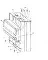
図1は、この発明の第1の実施形態によるGaN系半導体レーザの斜視図である。
【0034】
図1に示すように、この第1の実施形態によるGaN系半導体レーザにおいては、例えばc面のサファイア基板1上にレーザ構造を構成する複数の半導体層が積層された半導体層2が設けられている。この半導体層2は、GaN、AlGaN、GaInNなどの窒化物系III−V族化合物半導体からなる。また、この半導体層2は、pn接合を含んでいる。この半導体層2に設けられた共振器端面3(図1においては、前方の共振器端面のみが図示されている)は、窒化物系III−V族化合物半導体の劈開面である(11−20)面により構成されている。このGaN系半導体レーザにおいて、これらの共振器端面3は、ウェハ状のサファイア基板1上に半導体層2を積層した後、半導体層2の所定部分に劈開補助溝4を形成し、この劈開補助溝4から半導体層2およびサファイア基板1を劈開することにより形成されたものである。
【0035】
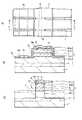
以下に、この第1の実施形態によるGaN系半導体レーザの詳細について、図2を参照して、その製造方法とともに説明する。ここで、図2Aは、このGaN系半導体レーザの製造の一工程におけるウェハの平面図、図2Bは、図2AのB−B線に沿った断面図、図2Cは、図2AのC−C線に沿った断面図である。
【0036】
図2に示すように、このGaN系半導体レーザの製造方法においては、例えば、c面のサファイア基板1上にMOCVD法により、レーザ構造を構成する半導体層2として、GaNバッファ層5、n型GaNコンタクト層6、n型AlGaNクラッド層7、GaN/GaInN多重量子井戸構造の活性層8、p型AlGaNクラッド層9およびp型GaNコンタクト層10を順次成長させる。ここで、GaNバッファ層5の厚さは例えば2μm、n型GaNコンタクト層6の厚さは例えば2μm、n型AlGaNクラッド層8の厚さは例えば0.5μm、p型AlGaNクラッド層9の厚さは例えば0.5μm、p型GaNコンタクト層10の厚さは例えば0.2μmである。
【0037】
次に、p型GaNコンタクト層10上に所定のストライプ形状のレジストパターン(図示せず)を形成した後、このレジストパターンをマスクとしてウエットエッチング法によりp型AlGaNクラッド層9の厚さ方向の途中の深さまでエッチングする。これによって、p型AlGaNクラッド層9の上層部およびp型GaNコンタクト層10が、一方向に延びる所定のリッジストライプ形状にパターニングされる。
【0038】
次に、このエッチングに用いたレジストパターンを除去し、p型AlGaNクラッド層9およびp型GaNコンタクト層10上に、リッジストライプ部11の延在する方向と平行な方向に延びる所定のストライプ形状のレジストパターン(図示せず)を形成した後、このレジストパターンをマスクとして例えばRIE法によりn型GaNコンタクト層6の厚さ方向の途中の深さまでエッチングすることにより溝を形成する。これにより、n型GaNコンタクト層6の上層部、n型AlGaNクラッド層7、活性層8およびp型AlGaNクラッド層9の下層部が、リッジストライプ部11の延在する方向と平行な方向に延在する所定のメサ形状にパターニングされる。
【0039】
なお、ここでは、レーザ構造を構成する半導体層2の劈開性を考慮して、c面のサファイア基板1上に成長された半導体層2に形成される共振器端面3が、半導体層2の劈開しやすい劈開面である(11−20)面にあたるように、予め、リッジストライプ部11およびメサ部12を形成する方位を決めておく。
【0040】
次に、このエッチングに用いたレジストパターンを除去した後、例えばCVD法により全面にSiO2膜のような絶縁層13を形成する。次に、リソグラフィーおよびエッチングにより、リッジストライプ部11の上側の部分における絶縁層13に開口13aを形成するとともに、溝の上側の所定部分における絶縁層13に開口13bを形成する。絶縁層13に形成されたこれらの開口13aおよび13bは、リッジストライプ部11およびメサ部12の延在する方向と平行な方向に延在する所定のストライプ形状を有する。
【0041】
次に、絶縁層13に形成された開口13aの部分におけるp型AlGaNクラッド層9の上層部およびp型GaNコンタクト層10上に、例えばNi/Ti/AuまたはNi/Pt/Auからなるp側電極14を形成するとともに、絶縁層13に形成された開口13bの部分におけるn型GaNコンタクト層6上に、例えばTi/Al/Pt/Auからなるn側電極15を形成する。
【0042】
次に、上述のようにしてウェハ状のサファイア基板1上にレーザ構造を形成した後、共振器端面3を形成すべき部分における半導体層2のうち、リッジストライプ部11およびメサ部12に対応する部分以外の部分、具体的には、メサ部12の両側の溝に対応する部分の一部を、例えばイオンミリング法のようなドライエッチング法により、例えばGaNバッファ層5の厚さ方向の途中の深さまでエッチングすることにより、この部分に、半導体層2の(11−20)面と平行な方向に延在する所定のストライプ状の劈開補助溝4を形成する。すなわち、この第1の実施形態においては、共振器端面3を形成すべき部分における半導体層2のうち、リッジストライプ部11およびメサ部12に対応する部分以外の部分に、メサ部12を両側から挟むようにして劈開補助溝4を形成する。図2C中、この劈開補助溝4を形成するためのエッチングによって除去された部分を、一点鎖線で示す。この場合、この劈開補助溝4は、後に共振器端面3となる部分のうち、光出射領域に対応する部分やpn接合の存在する部分には形成されておらず、GaN系半導体レーザの特性を何ら損なうものではない。図3は、この劈開補助溝4が形成された状態のウェハを示す斜視図である。
【0043】
ここで、この劈開補助溝4は、後に行われる劈開の際に、半導体層2およびサファイア基板1を、この劈開補助溝4に沿って容易にかつ確実に劈開することができるように、次のように構成されている。
【0044】
すなわち、この劈開補助溝4は、例えばV字型の断面形状を有し、後に行われる劈開の際に、その底部に応力集中が起こりやすいようにされている。上述のイオンミリング法では、エッチング異方性がないことや、エッチングマスクとなるレジストパターンとの選択性が小さいことなどの理由により、条件によって、このようなV字状の断面形状を有する劈開補助溝4を容易に形成することができる。また、この劈開補助溝4は、半導体層2の(11−20)面と平行な方向に延在する直線状の底部を有している。また、この劈開補助溝4の延長方向の先端部は、半導体層2の劈開位置の規定に有利に働くように、例えばV字状の平面形状を有している。なお、後に行われる劈開によって形成される共振器端面3の平坦性を良好にする観点から、同一部分の劈開に用いられる劈開補助溝4、特にその底部および延長方向の先端部は、同一直線上に存在することが好ましい。
【0045】
また、この第1の実施形態においては、後述のように、この劈開補助溝4に沿って共振器端面3が形成されることから、リッジストライプ部11およびメサ部12の延在する方向と平行な方向、したがって、最終的に製造されるGaN系半導体レーザの共振器長方向には、複数の劈開補助溝4が、最終的に製造されるGaN系半導体レーザの共振器長とほぼ同一間隔で、周期的に形成される。
【0046】
次に、上述のように半導体層2の所定部分に劈開補助溝4を形成した後、サファイア基板1を裏面側からラッピングすることにより、このサファイア基板1の厚さを例えば50〜150μm程度にする。
【0047】
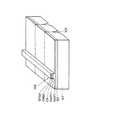
次に、ウェハ状のサファイア基板1をその上の半導体層2などとともに、劈開補助溝4に沿ってバー状に劈開することにより、半導体層2に両共振器端面3を形成する。この際、この第1の実施形態においては、次のようにしてサファイア基板1および半導体層2の劈開を行う。図4は、この第1の実施形態において、サファイア基板1および半導体層2を劈開補助溝4に沿って劈開するとき劈開方法を説明するための断面図である。図4においては、図2Bおよび図2Cと直交する方向の断面が示されている。
【0048】
すなわち、図4に示すように、この第1の実施形態においては、サファイア基板1および半導体層2を劈開補助溝4に沿って劈開する際に、例えば円形ローラー(図示せず)などの補助を用いて、劈開補助溝4が存在する側、したがって、半導体層2が積層された側の主面が凸となるような向きにサファイア基板1をたわませ、劈開補助溝4の底部に応力を集中させ、この劈開補助溝4から半導体層2およびサファイア基板1を劈開することにより、バーまたはチップ21を得るようにしている。
【0049】
ここで、サファイア基板1をいずれの方向に反らせても劈開は可能であるが、上述のように、劈開補助溝4が存在する側の主面が凸となるような向きにサファイア基板1を反らせ劈開を行っているのは、このようにした方が、これと反対の向きにサファイア基板1を反らせて劈開を行う場合よりも、半導体層2およびサファイア基板1が、所定の位置で割れやすくなるためである。
【0050】
上述のようにして、サファイア基板1および半導体層2をバー状に劈開し、半導体層2に劈開面からなる共振器端面3を形成した後、必要に応じて共振器端面3に端面コーティングを施し、さらに、この後、このバーをチップ化する。このチップ化は、ダイシングやスクライブによりバーを分離することにより行ってもよく、あるいは、予め、半導体層2の所定部分に、例えば共振器端面3となる半導体層2の(11−20)面に垂直な方向に延在する劈開補助溝を形成しておき、バーをこの劈開補助溝に沿って劈開することにより行ってもよい。
【0051】
以上のようにして、目的とするGaN系半導体レーザを完成させる。ここで、図2A中、一点鎖線によって囲まれた部分が、最終的に製造されるGaN系半導体レーザの一つのレーザチップに対応する。
【0052】
上述のように構成されたこの第1の実施形態によれば、サファイア基板1上にレーザ構造を構成する窒化物系III−V族化合物半導体からなる半導体層2を積層した後、共振器端面3を形成すべき部分における半導体層2の所定部分に劈開補助溝4を形成し、この劈開補助溝4から半導体層2およびサファイア基板1を劈開するようにしていることにより、半導体層2における劈開位置を規定しやすく、半導体層2およびサファイア基板1を容易にかつ確実に劈開することができる。このため、劈開性の無いサファイア基板1を用いた場合であっても、この上に積層された半導体層2に、光学的平坦性の優れた劈開面からなる共振器端面3を安定に形成することができ、しかも、共振器長を例えば1mm以下と小さくする場合であっても、そのような良好な共振器端面3を有するGaN系半導体レーザを、所望の共振器長で実現することができる。
【0053】
また、この第1の実施形態によれば、共振器端面3を形成すべき部分における半導体層2のうち、光出射領域となるリッジストライプ部11に対応する部分や、pn接合の存在するメサ部12に対応する部分以外の部分に劈開補助溝4を形成するようにしており、この部分では、劈開補助溝4をどの様な深さに形成しても、GaN系半導体レーザの特性は何ら損なわれないので、劈開補助溝4の形成する際の制御が容易であるという利点も有する。
【0054】
また、この第1の実施形態によれば、半導体層2に劈開補助溝4を形成し、劈開の際に、この半導体層2が積層された側の主面が凸になるようにサファイア基板1を反らせていることにより、劈開が半導体層2側から生じ、半導体層2における劈開位置の規定や、半導体層2に良好な劈開面を形成するのに有利である上に、半導体層2が積層された側の主面が凹になるようにサファイア基板1を反らせた場合に起こる可能性がある問題、具体的には、例えば、半導体層2、特にその最表面が圧縮され、これに起因して、半導体層2の表面付近がつぶれたり平坦性が劣化したりするという問題が生じないという利点も有する。
【0055】
さらに、この第1の実施形態によれば、劈開補助溝4は、イオンミリング法のようなウェハプロセスにおけるドライエッチング技術を用いて形成することができるため、劈開補助溝4を良好なパターン精度および寸法精度で形成することができ、また、例えば劈開補助溝4の平面パターンを破線状にするなど、素子構造に応じた微細加工を行うことも可能である。また、このように劈開補助溝4をドライエッチング技術を用いて形成することにより、従来のように、劈開補助溝の形成にダイシングやスクライブなどの機械加工を必要としないので、この機械加工の応力やダメージによるウェハの割れ欠けなどが発生しないという利点も有する。
【0056】
次に、この発明の第2の実施形態について説明する。図5は、この第2の実施形態によるGaN系半導体レーザの製造方法を説明するための平面図および断面図である。ここで、図5Aは、このGaN系半導体レーザの製造の一工程におけるウェハの平面図、図5Bは、図5AのB−B線に沿った断面図、図5Cは、図5AのC−C線に沿った断面図である。
【0057】
図5に示すように、この第2の実施形態においては、第1の実施形態と同様に工程を進めて、p型AlGaNクラッド層9の上層部およびp型GaNコンタクト層10を所定のリッジストライプ形状にパターニングする工程まで行う。
【0058】
次に、p型AlGaNクラッド層9およびp型GaNコンタクト層10上に、リッジストライプ部11の延在する方向と平行な方向に延在し、かつ、メサ部12の共振器端面3を形成すべき部分に対応する部分にV字状のくびれを有する所定のストライプ形状のレジストパターン(図示せず)を形成する。次に、このレジストパターンをマスクとしてRIE法により、n型GaNコンタクト層6の厚さ方向の途中の深さまでエッチングすることにより溝を形成する。これによって、n型GaNコンタクト層6の上層部、n型AlGaNクラッド層7、活性層8およびp型AlGaNクラッド層9の下層部が、リッジストライプ部11の延在する方向と平行な方向に延在する所定のメサ形状にパターニングされる。このメサ部12は、共振器端面3を形成すべき部分で両側がV字状にくびれた平面形状を有する。ただし、このメサ部12のくびれ12aの先端部は、リッジストライプ部11に達しないものとする。ここで、このメサ部12の互いに向かい合うくびれ12aの先端部同士を結ぶ直線は、後に共振器端面3となる半導体層2の(11−20)面と平行であることが好ましい。
【0059】
次に、第1の実施形態と同様に工程を進めて、p側電極14およびn側電極15の形成まで行った後、第1の実施形態と同様に、共振器端面3を形成すべき部分における半導体層2のうち、メサ部12の両側の溝に対応する部分の一部を、GaNバッファ層5の厚さ方向の途中の深さまでエッチングすることにより、この部分に、半導体層2の(11−20)面と平行な方向に延在する所定のストライプ状の劈開補助溝4を形成する。図5Cに、この劈開補助溝4を形成するためのエッチングによって除去された部分を、一点鎖線で示す。ここで、後に行われる劈開によって形成される共振器端面3の平坦性を良好にする観点から、同一部分の劈開に用いられる劈開補助溝4の底部および先端部、ならびに、メサ部12のくびれ12aの先端部は、同一直線上に存在することが好ましい。
【0060】
この後、第1の実施形態と同様に工程を進めて、目的とするGaN系半導体レーザを完成させる。ここで、図5A中、一点鎖線によって囲まれた部分が、最終的に製造されるGaN系半導体レーザの一つのレーザチップに対応する。
【0061】
この第2の実施形態の上記以外の構成は、第1の実施形態と同様であるので、説明を省略する。
【0062】
この第2の実施形態によれば、第1の実施形態と同様な利点を得ることができる。なお、この第2の実施形態においては、メサ部12が、共振器端面3を形成すべき部分で内側にくびれている分だけ、このメサ部12の両側に、第1の実施形態よりも先端部同士を近接させて劈開補助溝4を形成することができる。このため、共振器端面3を形成すべき部分における半導体層2のうち、劈開補助溝4の存在する部分の比率を、第1の実施形態に比べて大きくすることができるので、半導体層2およびサファイア基板1の劈開をより容易に行うことができる。また、メサ部12のうち、共振器端面3を形成すべき部分がV字状にくびれていることによっても劈開がより容易となる上に、半導体層2における劈開位置の規定もより容易となる。
【0063】
次に、この発明の第3の実施形態について説明する。図6は、この第3の実施形態によるGaN系半導体レーザの製造方法を説明するための平面図および断面図である。ここで、図6Aは、このGaN系半導体レーザの製造の一工程におけるウェハの平面図、図6Bは、図6AのB−B線に沿った断面図、図6Cは、図6AのC−C線に沿った断面図である。
【0064】
図6に示すように、この第3の実施形態においては、劈開補助溝4を、共振器端面3を形成すべき部分における半導体層2のうち、リッジストライプ部11に対応する部分以外の部分、具体的には、メサ部12に対応する部分の一部と、メサ部12の両側の溝に対応する部分とに、リッジストライプ部11を両側から挟むようにして形成する。
【0065】
すなわち、この第3の実施形態においては、第1の実施形態と同様に工程を進めて、p側電極14およびn側電極15の形成まで行った後、共振器端面3を形成すべき部分における半導体層2のうち、リッジストライプ部11に対応する部分以外の部分、具体的には、リッジストライプ部11の両側のメサ部12に対応する部分の一部と、メサ部12の両側の溝に対応する部分とを、例えばGaNバッファ層5の厚さ方向の途中の深さまでエッチングすることにより、この部分に、半導体層2の(11−20)面と平行な方向に延在する所定のストライプ状の劈開補助溝4を形成する。図6C中、劈開補助溝4を形成するためのエッチングによって除去された部分を、一点鎖線で示す。ここで、この劈開補助溝4は、メサ部12に対応する部分において、半導体層2のpn接合をまたぐ深さになっているが、この劈開補助溝4は、光出射領域となる部分には形成されていないので、このGaN系半導体レーザの特性を何ら損なうものではない。
【0066】
この後、第1の実施形態と同様に工程を進めて、目的とするGaN系半導体レーザを完成させる。図6A中、一点鎖線によって囲まれた部分が、最終的に製造されるGaN系半導体レーザの一つのレーザチップに対応する。
【0067】
この第3の実施形態によれば、第1の実施形態と同様の利点を得ることができる。なお、この第3の実施形態においては、共振器端面3を形成すべき部分における半導体層2に形成された劈開補助溝4が、メサ部12に対応する部分の一部まで延在しているため、リッジストライプ部11の両側に、第1の実施形態よりも先端部同士を近接させて劈開補助溝4を形成することができる。このため、共振器端面3を形成すべき部分における半導体層2のうち、劈開補助溝4の存在する部分の比率を、第1の実施形態に比べて大きくすることができるので、半導体層2およびサファイア基板1の劈開をより容易に行うことができる。
【0068】
次に、この発明の第4の実施形態について説明する。図7は、この第4の実施形態によるGaN系半導体レーザの製造方法を説明するための平面図および断面図である。ここで、図7Aは、このGaN系半導体レーザの製造の一工程におけるウェハの平面図、図7Bは、図7AのB−B線に沿った断面図、図7Cは、図7AのC−C線に沿った断面図である。
【0069】
図7に示すように、この第4の実施形態においては共振器端面3を形成すべき部分における半導体層2のうち、メサ部12の両側の溝に対応する部分に一部に、メサ部12を両側から挟むようにして劈開補助溝4を形成するとともに、リッジストライプ部11およびメサ部12に対応する部分にも劈開補助溝4を形成するようにしている。
【0070】
すなわち、この第4の実施形態においては、第1の実施形態と同様に工程を進めて、n側電極14およびp側電極15の形成まで行った後、共振器端面3を形成すべき部分における半導体層2のうち、メサ部12の両側の溝に対応する部分の一部を、GaNバッファ層5の厚さ方向の途中の深さまでエッチングすることにより、この部分に、メサ部12を両側から挟むようにして劈開補助溝4を形成するとともに、リッジストライプ部11に対応する部分をp型GaNコンタクト層10の厚さ方向の途中の深さまでエッチングし、それ以外のメサ部12に対応する部分をp型AlGaNクラッド層9の厚さ方向の途中の深さまでエッチングすることにより、リッジストライプ部11およびメサ部12に対応する部分にも劈開補助溝4を形成する。図7C中、この劈開補助溝4を形成するためのエッチングによって除去された部分を、一点鎖線で示す。
【0071】
ここで、リッジストライプ部11およびメサ部12に対応する部分に形成された劈開補助溝4は、劈開の際にその底部に応力集中が生じやすいように、例えばV字状の断面形状を有することが好ましい。なお、リッジストライプ部11に対応する部分に形成された劈開補助溝4の底部は、p型GaNコンタクト層10の厚さ方向の途中の深さに留められ、それ以外のメサ部12に対応する部分に形成された劈開補助溝4の底部は、p型AlGaNクラッド層9の厚さ方向の途中の深さに留められており、したがって、このリッジストライプ部11およびメサ部12に対応する部分に形成された劈開補助溝4は、光出射領域に到達する深さとはなっていないので、GaN系半導体レーザの特性を何ら損なうものではない。また、このリッジストライプ部11およびメサ部12に対応する部分における劈開補助溝4は、素子構造の都合などで、リッジストライプ部11およびメサ部12に対応する部分の一部のみに形成するようにしてもよい。
【0072】
この後、第1の実施形態と同様に工程を進めて、目的とするGaN系半導体レーザを完成させる。ここで、図7A中、一点鎖線によって囲まれた部分が、最終的に製造されるGaN系半導体レーザの一つのレーザチップに対応する。
【0073】
この第4の実施形態の上記以外の構成は、第1の実施形態と同様であるので、説明を省略する。
【0074】
この第4の実施形態によれば、第1の実施形態と同様の利点を得ることができる。なお、この第4の実施形態においては、劈開補助溝4がリッジストライプ部11およびメサ部12に対応する部分にも形成されており、したがって、共振器端面3を形成すべき部分に形成されている劈開補助溝4の比率が、第1の実施形態の場合よりも大きくされているため、サファイア基板1および半導体層2の劈開をより容易に行うことができる。
【0075】
以上この発明の実施形態について具体的に説明したが、この発明は、上述の実施形態に限定されるものではなく、この発明の技術的思想に基づく各種の変形が可能である。例えば、実施形態において挙げた数値、材料、構造、製造プロセスなどはあくまで例にすぎず、これに限定されるものではない。
【0076】
また、上述の第1〜第4の実施形態においては、劈開補助溝4の断面形状をV字状としているが、この劈開補助溝4の断面形状は、U字状、延長方向に平行な一側面を垂直面とする形状であってもよく、または、矩形状であってもよい。
【0077】
また、上述の第1〜第4の実施形態においては、メサ部12に対応する部分の両側における劈開補助溝4は、例えば、n型GaNコンタクト層6の厚さ方向の途中の深さまでエッチングすることにより形成してもよく、あるいは、GaNバッファ層5とサファイア基板1との界面までエッチングすることにより形成してもよい。また、第4の実施形態においては、リッジストライプ部11およびメサ部12に対応する部分における劈開補助溝4のうち、リッジストライプ部11に対応する部分以外の部分は、p型AlGaNクラッド層9を越えてエッチングすることにより形成してもよい。
【0078】
また、上述の第1〜第4の実施形態においては、窒化物系III−V族化合物半導体からなる半導体層2の成長にMOCVD法を用いているが、この半導体層2の成長には例えば分子線エピタキシー(MBE)法を用いてもよい。
【0079】
また、上述の第1〜第4の実施形態においては、この発明をリッジストライプ構造のGaN系半導体レーザに適用した場合について説明したが、この発明は、電極ストライプ構造のGaN系半導体レーザに適用することも可能である。
【0080】
また、上述の第1〜第4の実施形態においては、この発明をDH構造(Double Heterostructure)の半導体レーザに適用した場合について説明したが、この発明は、SCH構造(Separate Confinement Heterostructuer)の半導体レーザは勿論、発光ダイオードに適用することも可能であり、さらに、これらの半導体レーザや発光ダイオードのような半導体発光装置以外にも、フォトディテクタなどの半導体受光装置に適用することも可能である。
【0081】
さらに、この発明は、劈開性が無いか、劈開が困難か、あるいは、その上に成長される半導体層と異なる劈開方位を有する基板上に、劈開性を有する半導体層が成長された半導体装置において、半導体層に劈開面を形成する際の共通の技術であるので、この発明は、上記した半導体発光装置および半導体受光装置のような光半導体装置に留まらず、電界効果トランジスタなどの電子走行素子、または、複数の電子走行素子を集積した半導体集積回路、さらには、同一基板上に電子走行素子と光半導体装置とを集積した光電子集積回路など、半導体装置全般に適用することが可能であり、特に、チップサイズを微細寸法に規定したい半導体装置に適用した場合、顕著な効果を奏するものである。また、この発明は、窒化物系III−V族化合物半導体以外に、種々の材料を用いた半導体装置に適用することができる。
【0082】
【発明の効果】
以上のように、この発明の第1の発明、第3の発明および第5の発明によれば、端面を形成すべき部分における半導体層のうち、端面の主要部となる部分以外の部分の少なくとも一部に劈開補助溝を形成していることにより、また、この発明の第2の発明、第4の発明および第6の発明によれば、端面を形成すべき部分における半導体層の少なくとも一部に、pn接合をまたぐ深さで劈開補助溝を形成していることにより、半導体層における劈開位置を規定しやすく、しかも、この劈開補助溝から半導体層および基板を劈開することができるので、基板および半導体層の劈開を、劈開補助溝が形成された位置で、容易にかつ確実に行うことができる。このため、劈開性が無いか、劈開が困難か、または、この上の半導体層と異なる劈開方位を有する基板を用いた場合や、半導体装置の寸法を例えば1mm以下と小さく規定したい場合であっても、半導体層における劈開位置を規定しつつ、この半導体層に良好な劈開面からなる端面を制御性良く安定に形成することができ、これによって、光学的平坦性が良好な劈開面からなり、光学特性に優れた共振器端面を有する半導体レーザを実現することができる。
【0083】
また、この発明によれば、劈開補助溝を、ウェハプロセスによるドライエッチング技術を用いて形成することができるため、従来のようにダイシングやスクライブなどの機械加工によって劈開補助溝を形成する手法に比較して、劈開補助溝のパターン精度や微細加工性に優れ、また、機械的ダメージによるウェハの割れ欠けなどの問題が生じないため、安定して半導体装置を製造することができる。
【図面の簡単な説明】
【図1】 この発明の第1の実施形態によるGaN系半導体レーザの斜視図である。
【図2】 この発明の第1の実施形態によるGaN系半導体レーザの製造方法を説明するための平面図および断面図である。
【図3】 この発明の第1の実施形態によるGaN系半導体レーザの製造方法を説明するための斜視図である。
【図4】 この発明の第1の実施形態によるGaN系半導体レーザの製造方法を説明するための断面図である。
【図5】 この発明の第2の実施形態によるGaN系半導体レーザの製造方法を説明するための平面図および断面図である。
【図6】 この発明の第3の実施形態によるGaN系半導体レーザの製造方法を説明するための平面図および断面図である。
【図7】 この発明の第4の実施形態によるGaN系半導体レーザの製造方法を説明するための平面図および断面図である。
【図8】 従来のGaN系半導体レーザの製造方法を説明するための斜視図である。
【符号の説明】
1・・・サファイア基板、2・・・半導体層、3・・・共振器端面、4・・・劈開補助溝、5・・・GaNバッファ層、6・・・n型GaNコンタクト層、7・・・n型AlGaNクラッド層、8・・・活性層、9・・・p型AlGaNクラッド層、10・・・p型GaNコンタクト層、11・・・リッジストライプ部、12・・・メサ部、12a・・・くびれ、13・・・絶縁層、13a,13b・・・開口、14・・・p側電極、15・・・n側電極[0001]
BACKGROUND OF THE INVENTION
The present invention relates to a semiconductor device and a method for manufacturing the same.To the lawIn particular, a semiconductor device such as a semiconductor laser in which a cavity end face is formed by cleavage.In placeIt is suitable for application.
[0002]
[Prior art]
Nitride III-V compound semiconductors composed of group III elements such as gallium (Ga), aluminum (Al), indium (In) and the like and group V elements of nitrogen (N), such as GaN, AlGaN, GaInN, etc. Since it is a direct transition semiconductor and has a larger band gap than semiconductors already used in semiconductor lasers such as AlGaInAs and AlGaInP, a short wavelength semiconductor laser having an emission wavelength of 400 nm, ultraviolet to green Widely applied to light sources used in highly integrated and high-density optical disk playback devices, optical devices used in full-color display elements, and the like, such as light-emitting diodes (LEDs) that can emit light at low temperatures. The nitride III-V compound semiconductor is also attracting attention as a material for an electron transit device such as a high-power, high-frequency field effect transistor (FET) because of its high saturation electron velocity in a high electric field.
[0003]
Semiconductor lasers, light emitting diodes, FETs, and the like using this nitride III-V compound semiconductor are, for example, sapphire (Al2OThree) It is manufactured by epitaxially growing a nitride III-V compound semiconductor on a substrate such as a substrate.
[0004]
By the way, in general, in a semiconductor laser, it is necessary to form a resonator end face. In an AlGaInAs-based, AlGaInP-based, or InP-based semiconductor laser, a substrate and a semiconductor layer grown on the substrate have a cleavage property, and the cleavage plane is often used as a resonator end surface of the semiconductor laser.
[0005]
On the other hand, nitride III-V compound semiconductors generally have a crystal structure of a hexagonal wurtzite structure, so that it is generally difficult to obtain a stable cleavage plane. Further, the semiconductor laser using the nitride III-V compound semiconductor is often manufactured by growing a nitride III-V compound semiconductor on the sapphire substrate as described above. However, it has been difficult to form a semiconductor laser having a cleavage plane as a cavity end face.
[0006]
Here, for example, in Japanese Patent Laid-Open Nos. 8-222807 and 9-172223, a resonator end face is formed by cleaving a sapphire substrate and a semiconductor layer made of a III-V group compound semiconductor laminated thereon. A method of manufacturing a GaN-based semiconductor laser that is formed is disclosed.
[0007]
That is, in this conventional method for manufacturing a GaN-based semiconductor laser, as shown in FIG. 8, a GaN
[0008]
Next, after forming a resist pattern (not shown) having a predetermined stripe shape on the p-type
[0009]
Next, after removing the resist pattern, a p-side electrode (not shown) is formed on the p-type
[0010]
Next, the thickness of the
[0011]
Next, the
[0012]
According to this conventional method for manufacturing a GaN-based semiconductor laser, a resonance consisting of a cleaved surface (pseudo-cleaved surface) with excellent optical characteristics as compared with the case where a cavity end face is formed by etching in a semiconductor layer constituting a laser structure. A vessel end face can be formed.
[0013]
[Problems to be solved by the invention]
However, the conventional GaN semiconductor laser manufacturing method described above has the following problems.
[0014]
That is, the optical resonator length of a semiconductor laser is usually designed to be 1 mm or less, particularly in the range of about 0.2 to 0.7 mm. However, in order to reduce the optical resonator length to this value, it is necessary to reduce the thickness of the
[0015]
Further, since the
[0016]
However, since the strength of the
[0017]
Accordingly, an object of the present invention is to form an end face made of a cleavage plane in a semiconductor layer laminated on a substrate, and at this time, there is no cleavage property, cleavage is difficult, or the cleavage direction is different from that of the semiconductor layer. A semiconductor device capable of stably forming a good cleavage surface in a semiconductor layer with good controllability even when a substrate is used or when the size of the semiconductor device is desired to be as small as 1 mm or less, and a method for manufacturing the sameThe lawIt is to provide.
[0018]
[Means for Solving the Problems]
In order to achieve the above object, the first invention of the present invention provides:
A semiconductor layer having a cleavage property is stacked on the substrate,
In the semiconductor device having a semiconductor layer having an end face made of a cleavage plane,
The end face of the semiconductor layer is laminated on the substrate.After the mesa portion is formed in the semiconductor layer, a cleavage assisting groove is formed from the mesa portion other than the portion that becomes the light emitting region or the light incident region on the end surface to the portion other than the mesa portion in the semiconductor layer.It is formed by dry etching and cleaving the semiconductor layer and the substrate from this cleavage assisting groove.
It is characterized by this.
[0021]
No. 1 of this invention2The invention of
A semiconductor layer having a cleavage property is stacked on the substrate,
In the semiconductor device having a semiconductor layer having an end face made of a cleavage plane,
As for the end face of the semiconductor layer, after laminating the semiconductor layer on the substrate and forming the mesa portion on the semiconductor layer, the cleaving assistance is performed so that the mesa portion is sandwiched from both sides of at least a part of the semiconductor layer other than the mesa portion. Grooves are formed by dry etching, and the mesa has a planar shape that is constricted in a V shape on both sides on the same straight line as the cleavage assisting groove, and is formed by cleaving the semiconductor layer and the substrate from the cleavage assisting groove. Is
It is characterized by this.
[0023]
The third invention of the present invention is:
In a method for manufacturing a semiconductor device, a semiconductor layer having a cleavage property is laminated on a substrate, and the semiconductor layer has an end face made of a cleavage plane.
Laminating a semiconductor layer on a substrate;
Forming a mesa portion in the semiconductor layer;
A step of forming a cleavage assisting groove by dry etching across a portion other than the mesa portion from the mesa portion other than the portion that becomes the light emitting region or the light incident region of the end surface of the semiconductor layer;
Forming an end face in the semiconductor layer by cleaving the semiconductor layer and the substrate from the cleavage assist groove;
It is characterized by having.
No. 1 of this invention4The invention of
In a method for manufacturing a semiconductor device, a semiconductor layer having a cleavage property is laminated on a substrate, and the semiconductor layer has an end face made of a cleavage plane.
Laminating a semiconductor layer on a substrate;
Forming a mesa portion in the semiconductor layer;
Forming a cleavage assisting groove by dry etching so as to sandwich the mesa portion from both sides in at least a part of the semiconductor layer other than the mesa portion;
Cleaving the semiconductor layer and the substrate from the cleavage assisting groove to form an end face in the semiconductor layer,
The mesa portion is characterized in that both sides have a planar shape constricted in a V shape on the same straight line as the cleavage assisting groove.
[0024]
In this invention, the cross-sectional shape of the cleavage assisting groove may be rectangular, for example, but from the viewpoint of easily defining the cleavage position and the process when cleaving the semiconductor layer and the substrate, the section of the cleavage assisting groove The shape is preferably a V-shaped, U-shaped, or a shape in which one side parallel to the extending direction is a vertical surface, such that stress concentration is likely to occur at the bottom during cleavage.
[0025]
In the present invention, the main part of the end face differs depending on the type of semiconductor device. For example, a semiconductor device in which light is emitted or incident through the end face of the semiconductor layer, specifically, an optical semiconductor device such as a semiconductor light emitting device such as a semiconductor laser or a light emitting diode, or a semiconductor light receiving device such as a photodetector. In, the main portion of the end face refers to a portion that becomes a light emitting region or a light incident region, and more preferably a portion that includes a portion in the vicinity thereof. On the other hand, in an electron transit element such as a field effect transistor, or a semiconductor integrated circuit in which a plurality of electron transit elements are integrated, for example, it refers to the central portion of the structure when formed into a chip.
[0026]
In the present invention, when the semiconductor device is an optical semiconductor device having a light emitting region or a light incident region on the end face, the cleavage assisting groove is formed on the end face from the viewpoint of not impairing the characteristics of the optical semiconductor device. It is formed in a portion other than a portion that becomes an emission region or a light incident region. In this case, in the first invention, the third invention, and the fifth invention, the cleavage assisting groove is formed in the light emitting region or the light in the portion immediately above the portion that becomes the light emitting region or the light incident region on the end face. You may make it form so that the part used as an incident area may not be reached.
[0027]
In the present invention, the material of the semiconductor layer includes, for example, at least one group III element selected from the group consisting of Ga, Al, In, and B, at least N, and optionally V or As or P. A nitride III-V compound semiconductor composed of a group element can be used. Specific examples of the nitride III-V compound semiconductor include GaN, AlGaN, GaInN, and AlGaInN. In the present invention, for example, a substrate that does not have cleavage property, is difficult to cleave, or has a cleavage direction different from that of the semiconductor layer laminated thereon can be used. A specific example of such a substrate is a sapphire substrate used in a semiconductor device such as a semiconductor laser using the nitride III-V compound semiconductor described above.
[0028]
In the third invention, the fourth invention, the fifth invention and the sixth invention of this invention, it is preferable that the cleavage assisting groove extends in a direction parallel to the cleavage plane of the semiconductor layer. It is preferable that the auxiliary grooves are periodically formed at substantially the same interval in a direction perpendicular to the cleavage plane of the semiconductor layer.
[0029]
According to the first, third, and fifth aspects of the present invention configured as described above, the semiconductor layer in the portion where the end surface is to be formed, except for the portion that becomes the main portion of the end surface By forming the cleavage assisting groove in at least a part of the substrate, it is easy to define the cleavage position in the semiconductor layer, and the semiconductor layer and the substrate can be cleaved from the cleavage assisting groove. The cleavage can be easily and reliably performed at the position where the cleavage assist groove is formed. For this reason, there is no cleaving, it is difficult to cleave, or when a substrate having a cleavage orientation different from that of the semiconductor layer above is used, or when it is desired to define the size of the semiconductor device as small as 1 mm or less, for example. However, it is possible to stably form an end face made of a good cleavage plane in the semiconductor layer while defining the cleavage position in the semiconductor layer. In addition, in this case, since the cleavage assist groove is formed in a portion other than the main portion of the end face, the cleavage plane is formed in the semiconductor layer without impairing the characteristics of the semiconductor device to be manufactured. Can do.
[0030]
According to the second, fourth, and sixth aspects of the present invention configured as described above, at least a part of the semiconductor layer in the portion where the end face is to be formed has a depth across the pn junction. By forming the cleavage assisting groove, the cleavage position in the semiconductor layer can be easily defined, and the semiconductor layer and the substrate can be cleaved from the cleavage assisting groove. It can be carried out easily and reliably at the position where the cleavage assisting groove is formed. For this reason, there is no cleaving, it is difficult to cleave, or when a substrate having a cleavage orientation different from that of the semiconductor layer above is used, or when it is desired to define the size of the semiconductor device as small as 1 mm or less, for example. However, it is possible to stably form an end face made of a good cleavage plane in the semiconductor layer while defining the cleavage position in the semiconductor layer. In this case, the cleavage assisting groove is formed deeper in the semiconductor layer than in the case where the cleavage assisting groove is formed at a depth that does not reach the pn junction, so that the cleavage of the substrate and the semiconductor layer is easier. Can be done.
[0031]
In the present invention, since the cleavage assisting groove is formed in the semiconductor layer, the cleavage assisting groove can be formed using a dry etching technique based on a wafer process. For this reason, the cleavage assisting groove can be formed with good pattern accuracy, and fine processing such as making the cleavage assisting groove into a broken line shape can also be performed. In addition, since there is no need for machining steps such as dicing and scribing as in the past, even if the substrate thickness is small and the strength is not strong, there is a problem of chipping of the substrate related to the formation of the cleavage assist groove. Does not occur.
[0032]
DETAILED DESCRIPTION OF THE INVENTION
Hereinafter, embodiments of the present invention will be described with reference to the drawings. In all the drawings of the embodiments, the same or corresponding parts are denoted by the same reference numerals.
[0033]
FIG. 1 is a perspective view of a GaN semiconductor laser according to the first embodiment of the present invention.
[0034]
As shown in FIG. 1, in the GaN-based semiconductor laser according to the first embodiment, for example, a
[0035]
The details of the GaN-based semiconductor laser according to the first embodiment will be described below together with its manufacturing method with reference to FIG. Here, FIG. 2A is a plan view of the wafer in one step of manufacturing the GaN-based semiconductor laser, FIG. 2B is a cross-sectional view taken along the line BB of FIG. 2A, and FIG. 2C is a cross-sectional view of FIG. It is sectional drawing along a line.
[0036]
As shown in FIG. 2, in this GaN semiconductor laser manufacturing method, for example, a
[0037]
Next, after forming a resist pattern (not shown) having a predetermined stripe shape on the p-type
[0038]
Next, the resist pattern used in this etching is removed, and a predetermined stripe shape extending in a direction parallel to the extending direction of the
[0039]
Here, in consideration of the cleaving property of the
[0040]
Next, after removing the resist pattern used for this etching, the entire surface is
[0041]
Next, on the upper layer portion of the p-type
[0042]
Next, after the laser structure is formed on the wafer-
[0043]
Here, the cleavage assisting groove 4 is formed in the following manner so that the
[0044]
In other words, the cleavage assisting groove 4 has, for example, a V-shaped cross-sectional shape, and stress concentration is likely to occur at the bottom when cleavage is performed later. In the above-described ion milling method, the cleavage assist having such a V-shaped cross-sectional shape depending on conditions due to lack of etching anisotropy and low selectivity with a resist pattern serving as an etching mask. The groove 4 can be easily formed. The cleavage assisting groove 4 has a linear bottom extending in a direction parallel to the (11-20) plane of the
[0045]
In the first embodiment, since the resonator end face 3 is formed along the cleavage assisting groove 4 as will be described later, the
[0046]
Next, after forming the cleavage assisting groove 4 in a predetermined portion of the
[0047]
Next, both the resonator end faces 3 are formed in the
[0048]
That is, as shown in FIG. 4, in the first embodiment, when the
[0049]
Here, the
[0050]
As described above, the
[0051]
As described above, the target GaN semiconductor laser is completed. Here, in FIG. 2A, a portion surrounded by a one-dot chain line corresponds to one laser chip of a GaN-based semiconductor laser that is finally manufactured.
[0052]
According to the first embodiment configured as described above, after laminating the
[0053]
Further, according to the first embodiment, in the
[0054]
Further, according to the first embodiment, the cleavage assisting groove 4 is formed in the
[0055]
Furthermore, according to the first embodiment, the cleavage assisting groove 4 can be formed by using a dry etching technique in a wafer process such as an ion milling method. It can be formed with dimensional accuracy, and fine processing according to the element structure can be performed, for example, the planar pattern of the cleavage assisting groove 4 is made into a broken line shape. Further, by forming the cleavage assisting groove 4 by using the dry etching technique in this way, the machining assisting groove is not required to be machined such as dicing or scribe to form the cleavage assisting groove. In addition, there is an advantage that the wafer is not broken or chipped due to damage.
[0056]
Next explained is the second embodiment of the invention. FIGS. 5A and 5B are a plan view and a cross-sectional view for explaining the manufacturing method of the GaN-based semiconductor laser according to the second embodiment. Here, FIG. 5A is a plan view of the wafer in one step of manufacturing the GaN-based semiconductor laser, FIG. 5B is a cross-sectional view taken along line BB in FIG. 5A, and FIG. 5C is a cross-sectional view along CC in FIG. It is sectional drawing along a line.
[0057]
As shown in FIG. 5, in the second embodiment, the process proceeds in the same manner as in the first embodiment, and the upper layer portion of the p-type
[0058]
Next, on the p-type
[0059]
Next, the process proceeds in the same manner as in the first embodiment, and after forming the p-
[0060]
Thereafter, the process proceeds in the same manner as in the first embodiment to complete the target GaN-based semiconductor laser. Here, in FIG. 5A, a portion surrounded by a one-dot chain line corresponds to one laser chip of a GaN-based semiconductor laser that is finally manufactured.
[0061]
Since the other configuration of the second embodiment is the same as that of the first embodiment, description thereof is omitted.
[0062]
According to the second embodiment, the same advantages as those of the first embodiment can be obtained. In the second embodiment, the tip of the
[0063]
Next explained is the third embodiment of the invention. FIGS. 6A and 6B are a plan view and a cross-sectional view for explaining a method for manufacturing a GaN-based semiconductor laser according to the third embodiment. Here, FIG. 6A is a plan view of the wafer in one step of manufacturing the GaN-based semiconductor laser, FIG. 6B is a cross-sectional view taken along line BB of FIG. 6A, and FIG. 6C is a cross-sectional view of FIG. It is sectional drawing along a line.
[0064]
As shown in FIG. 6, in the third embodiment, the cleavage assisting groove 4 is formed in a portion other than the portion corresponding to the
[0065]
That is, in the third embodiment, the process proceeds in the same manner as in the first embodiment until the formation of the p-
[0066]
Thereafter, the process proceeds in the same manner as in the first embodiment to complete the target GaN-based semiconductor laser. In FIG. 6A, a part surrounded by a one-dot chain line corresponds to one laser chip of a GaN-based semiconductor laser that is finally manufactured.
[0067]
According to the third embodiment, the same advantages as those of the first embodiment can be obtained. In the third embodiment, the cleavage assisting groove 4 formed in the
[0068]
Next explained is the fourth embodiment of the invention. 7A and 7B are a plan view and a cross-sectional view for explaining a method for manufacturing a GaN-based semiconductor laser according to the fourth embodiment. Here, FIG. 7A is a plan view of the wafer in one step of manufacturing this GaN-based semiconductor laser, FIG. 7B is a cross-sectional view taken along line BB in FIG. 7A, and FIG. 7C is a cross-sectional view along CC in FIG. It is sectional drawing along a line.
[0069]
As shown in FIG. 7, in the fourth embodiment, a portion of the
[0070]
That is, in the fourth embodiment, the process proceeds in the same manner as in the first embodiment until the formation of the n-
[0071]
Here, the cleavage assisting groove 4 formed in the portion corresponding to the
[0072]
Thereafter, the process proceeds in the same manner as in the first embodiment to complete the target GaN-based semiconductor laser. Here, in FIG. 7A, the part surrounded by the alternate long and short dash line corresponds to one laser chip of the GaN-based semiconductor laser that is finally manufactured.
[0073]
Since the configuration of the fourth embodiment other than the above is the same as that of the first embodiment, description thereof is omitted.
[0074]
According to the fourth embodiment, the same advantages as those of the first embodiment can be obtained. In the fourth embodiment, the cleavage assisting grooves 4 are also formed in the portions corresponding to the
[0075]
Although the embodiments of the present invention have been specifically described above, the present invention is not limited to the above-described embodiments, and various modifications based on the technical idea of the present invention are possible. For example, the numerical values, materials, structures, manufacturing processes, and the like given in the embodiments are merely examples, and the present invention is not limited to these.
[0076]
In the first to fourth embodiments described above, the cross-sectional shape of the cleavage assisting groove 4 is V-shaped. The cross-sectional shape of the cleavage assisting groove 4 is U-shaped, one parallel to the extending direction. The side surface may be a vertical surface or a rectangular shape.
[0077]
In the first to fourth embodiments described above, the cleavage assisting grooves 4 on both sides of the portion corresponding to the
[0078]
In the first to fourth embodiments described above, the MOCVD method is used for the growth of the
[0079]
In the first to fourth embodiments, the case where the present invention is applied to a GaN-based semiconductor laser having a ridge stripe structure has been described. However, the present invention is applied to a GaN-based semiconductor laser having an electrode stripe structure. It is also possible.
[0080]
In the above first to fourth embodiments, the case where the present invention is applied to a semiconductor laser having a DH structure (Double Heterostructure) has been described. However, the present invention relates to a semiconductor laser having an SCH structure (Separate Confinement Heterostructuer). Needless to say, the present invention can be applied to a light emitting diode, and besides a semiconductor light emitting device such as a semiconductor laser or a light emitting diode, it can also be applied to a semiconductor light receiving device such as a photodetector.
[0081]
Furthermore, the present invention relates to a semiconductor device in which a semiconductor layer having a cleavage property is grown on a substrate that has no cleavage property, is difficult to cleave, or has a cleavage orientation different from that of a semiconductor layer grown thereon. Since this is a common technique for forming a cleavage plane in a semiconductor layer, the present invention is not limited to an optical semiconductor device such as the semiconductor light emitting device and the semiconductor light receiving device described above, but an electron transit element such as a field effect transistor, Or, it can be applied to semiconductor devices in general, such as a semiconductor integrated circuit in which a plurality of electron transit elements are integrated, and an optoelectronic integrated circuit in which an electron transit element and an optical semiconductor device are integrated on the same substrate. When applied to a semiconductor device in which the chip size is desired to be defined as a fine size, a remarkable effect can be obtained. Further, the present invention can be applied to semiconductor devices using various materials other than the nitride-based III-V compound semiconductor.
[0082]
【The invention's effect】
As described above, according to the first invention, the third invention, and the fifth invention of the present invention, at least a portion of the semiconductor layer in the portion where the end face is to be formed, other than the main portion of the end face. According to the second, fourth and sixth aspects of the present invention, at least a part of the semiconductor layer in the portion where the end face is to be formed In addition, since the cleavage assisting groove is formed at a depth across the pn junction, the cleavage position in the semiconductor layer can be easily defined, and the semiconductor layer and the substrate can be cleaved from the cleavage assisting groove. Further, the cleavage of the semiconductor layer can be easily and reliably performed at the position where the cleavage assisting groove is formed. For this reason, there is no cleaving, it is difficult to cleave, or when a substrate having a cleavage orientation different from that of the semiconductor layer above is used, or when it is desired to define the size of the semiconductor device as small as 1 mm or less, for example. In addition, while defining the cleavage position in the semiconductor layer, it is possible to stably and stably form an end face made of a good cleavage surface in this semiconductor layer, thereby comprising a cleavage surface with good optical flatness, A semiconductor laser having a resonator end face with excellent optical characteristics can be realized.
[0083]
In addition, according to the present invention, the cleavage assist groove can be formed by using a dry etching technique based on a wafer process, so that it is compared with a conventional method of forming the cleavage assist groove by machining such as dicing or scribing. As a result, the cleaving assist groove has excellent pattern accuracy and fine processability, and does not suffer from problems such as cracking of the wafer due to mechanical damage. Therefore, a semiconductor device can be manufactured stably.
[Brief description of the drawings]
FIG. 1 is a perspective view of a GaN semiconductor laser according to a first embodiment of the invention.
FIGS. 2A and 2B are a plan view and a cross-sectional view for explaining a method for manufacturing a GaN-based semiconductor laser according to the first embodiment of the invention. FIGS.
FIG. 3 is a perspective view for explaining the method for manufacturing the GaN-based semiconductor laser according to the first embodiment of the invention.
FIG. 4 is a cross-sectional view for explaining the method for manufacturing the GaN-based semiconductor laser according to the first embodiment of the invention.
5A and 5B are a plan view and a cross-sectional view for explaining a GaN semiconductor laser manufacturing method according to a second embodiment of the invention.
6A and 6B are a plan view and a cross-sectional view for explaining a GaN semiconductor laser manufacturing method according to a third embodiment of the invention.
7A and 7B are a plan view and a cross-sectional view for explaining a GaN-based semiconductor laser manufacturing method according to a fourth embodiment of the invention.
FIG. 8 is a perspective view for explaining a conventional method of manufacturing a GaN-based semiconductor laser.
[Explanation of symbols]
DESCRIPTION OF
Claims (16)
Translated fromJapanese上記半導体層は劈開面からなる端面を有する半導体装置において、In the semiconductor device having an end face made of a cleavage plane, the semiconductor layer
上記半導体層の上記端面は、上記基板上に上記半導体層を積層し、上記半導体層にメサ部を形成した後、上記半導体層のうち、上記端面の光出射領域または光入射領域となる部分以外の上記メサ部から上記メサ部以外の部分にまたがって劈開補助溝をドライエッチングにより形成し、この劈開補助溝から上記半導体層および上記基板を劈開することにより形成されたものであるThe end surface of the semiconductor layer is a portion other than a portion of the semiconductor layer that becomes a light emitting region or a light incident region after the semiconductor layer is stacked on the substrate and a mesa portion is formed on the semiconductor layer. A cleavage assisting groove is formed by dry etching from the mesa part to a part other than the mesa part, and the semiconductor layer and the substrate are cleaved from the cleavage assisting groove.
ことを特徴とする半導体装置。A semiconductor device.
上記半導体層は劈開面からなる端面を有する半導体装置において、In the semiconductor device having an end face made of a cleavage plane, the semiconductor layer
上記半導体層の上記端面は、上記基板上に上記半導体層を積層し、上記半導体層にメサ部を形成した後、上記半導体層のうち、上記メサ部以外の部分の少なくとも一部に上記メサ部を両側から挟み込むように劈開補助溝をドライエッチングにより形成し、上記メサ部は両側が上記劈開補助溝と同一直線上でV字状にくびれた平面形状を有し、上記劈開補助溝から上記半導体層および上記基板を劈開することにより形成されたものであるThe end surface of the semiconductor layer is formed by laminating the semiconductor layer on the substrate and forming a mesa portion on the semiconductor layer, and then forming the mesa portion on at least a part of the semiconductor layer other than the mesa portion. The cleaved auxiliary groove is formed by dry etching so as to sandwich the film from both sides, and the mesa portion has a planar shape that is constricted in a V shape on both sides on the same straight line as the cleaved auxiliary groove. Formed by cleaving the layer and the substrate
ことを特徴とする半導体装置。A semiconductor device.
上記基板上に上記半導体層を積層する工程と、Laminating the semiconductor layer on the substrate;
上記半導体層にメサ部を形成する工程と、Forming a mesa portion in the semiconductor layer;
上記半導体層のうち、上記端面の光出射領域または光入射領域となる部分以外の上記メサ部から上記メサ部以外の部分にまたがって劈開補助溝をドライエッチングにより形成する工程と、A step of forming, by dry etching, a cleavage assisting groove extending from the mesa portion other than the portion that becomes the light emitting region or the light incident region of the end face to the portion other than the mesa portion, of the semiconductor layer;
上記劈開補助溝から上記半導体層および上記基板を劈開することにより、上記半導体層に上記端面を形成する工程とForming the end face in the semiconductor layer by cleaving the semiconductor layer and the substrate from the cleavage assisting groove;
を有することを特徴とする半導体装置の製造方法。A method for manufacturing a semiconductor device, comprising:
上記基板上に上記半導体層を積層する工程と、Laminating the semiconductor layer on the substrate;
上記半導体層にメサ部を形成する工程と、Forming a mesa portion in the semiconductor layer;
上記半導体層のうち、上記メサ部以外の部分の少なくとも一部に上記メサ部を両側から挟み込むように劈開補助溝をドライエッチングにより形成する工程と、Forming a cleavage assisting groove by dry etching so as to sandwich the mesa part from both sides in at least a part of the semiconductor layer other than the mesa part;
上記劈開補助溝から上記半導体層および上記基板を劈開することにより、上記半導体層に上記端面を形成する工程とを有し、Cleaving the semiconductor layer and the substrate from the cleavage assisting groove to form the end face in the semiconductor layer,
上記メサ部は両側が上記劈開補助溝と同一直線上でV字状にくびれた平面形状を有することを特徴とする半導体装置の製造方法。The method for manufacturing a semiconductor device, wherein the mesa portion has a planar shape with both sides constricted in a V shape on the same straight line as the cleavage assisting groove.
Priority Applications (9)
| Application Number | Priority Date | Filing Date | Title |
|---|---|---|---|
| JP05527298AJP3822976B2 (en) | 1998-03-06 | 1998-03-06 | Semiconductor device and manufacturing method thereof |
| US09/260,138US6278173B1 (en) | 1998-03-06 | 1999-03-01 | Semiconductor device, its manufacturing method and substrate for manufacturing a semiconductor device |
| TW088103248ATW437134B (en) | 1998-03-06 | 1999-03-03 | Semiconductor device, its manufacturing method and substrate for manufacturing a semiconductor device |
| MYPI99000819AMY122220A (en) | 1998-03-06 | 1999-03-05 | Semiconductor device, its manufacturing method and substrate for manufacturing a semiconductor device |
| CNB991056116ACN100541815C (en) | 1998-03-06 | 1999-03-05 | Semiconductor device, manufacturing method thereof, and substrate for manufacturing semiconductor device |
| KR1019990007473AKR100681987B1 (en) | 1998-03-06 | 1999-03-06 | Semiconductor device, manufacturing method thereof and substrate for manufacturing semiconductor device |
| SG1999001313ASG77227A1 (en) | 1998-03-06 | 1999-03-06 | Semiconductor device its manufacturing method and substrate for manufacturing a semiconductor device |
| US09/712,392US6482666B1 (en) | 1998-03-06 | 2000-11-14 | Semiconductor device, its manufacturing method and substrate for manufacturing a semiconductor device |
| US09/840,199US6455342B2 (en) | 1998-03-06 | 2001-04-23 | Semiconductor device, its manufacturing method and substrate for manufacturing a semiconductor device |
Applications Claiming Priority (1)
| Application Number | Priority Date | Filing Date | Title |
|---|---|---|---|
| JP05527298AJP3822976B2 (en) | 1998-03-06 | 1998-03-06 | Semiconductor device and manufacturing method thereof |
Publications (2)
| Publication Number | Publication Date |
|---|---|
| JPH11251265A JPH11251265A (en) | 1999-09-17 |
| JP3822976B2true JP3822976B2 (en) | 2006-09-20 |
Family
ID=12993975
Family Applications (1)
| Application Number | Title | Priority Date | Filing Date |
|---|---|---|---|
| JP05527298AExpired - LifetimeJP3822976B2 (en) | 1998-03-06 | 1998-03-06 | Semiconductor device and manufacturing method thereof |
Country Status (7)
| Country | Link |
|---|---|
| US (3) | US6278173B1 (en) |
| JP (1) | JP3822976B2 (en) |
| KR (1) | KR100681987B1 (en) |
| CN (1) | CN100541815C (en) |
| MY (1) | MY122220A (en) |
| SG (1) | SG77227A1 (en) |
| TW (1) | TW437134B (en) |
Families Citing this family (47)
| Publication number | Priority date | Publication date | Assignee | Title |
|---|---|---|---|---|
| JP2000323789A (en)* | 1999-05-11 | 2000-11-24 | Nec Corp | Window-type semiconductor laser and manufacture |
| JP2001094212A (en)* | 1999-09-24 | 2001-04-06 | Sanyo Electric Co Ltd | Semiconductor device and method of manufacturing the same |
| US6614056B1 (en)* | 1999-12-01 | 2003-09-02 | Cree Lighting Company | Scalable led with improved current spreading structures |
| US6653663B2 (en)* | 1999-12-06 | 2003-11-25 | Matsushita Electric Industrial Co., Ltd. | Nitride semiconductor device |
| JP4060511B2 (en)* | 2000-03-28 | 2008-03-12 | パイオニア株式会社 | Method for separating nitride semiconductor device |
| JP3889933B2 (en)* | 2001-03-02 | 2007-03-07 | シャープ株式会社 | Semiconductor light emitting device |
| JP4066681B2 (en)* | 2001-03-21 | 2008-03-26 | 日亜化学工業株式会社 | Light emitting device and method for manufacturing light emitting device |
| JP2002289955A (en)* | 2001-03-23 | 2002-10-04 | Sharp Corp | Semiconductor laser element, manufacturing method therefor and optical information reproducing device |
| JP3912044B2 (en)* | 2001-06-06 | 2007-05-09 | 豊田合成株式会社 | Method for manufacturing group III nitride compound semiconductor light emitting device |
| JP2003017791A (en) | 2001-07-03 | 2003-01-17 | Sharp Corp | Nitride semiconductor device and method for manufacturing the nitride semiconductor device |
| GB0124427D0 (en)* | 2001-10-11 | 2001-12-05 | Eblana Photonics Ltd | A method of manufacturing a semiconductor device |
| JP3878868B2 (en) | 2002-03-01 | 2007-02-07 | シャープ株式会社 | GaN-based laser element |
| SG130935A1 (en)* | 2002-06-26 | 2007-04-26 | Agency Science Tech & Res | Method of cleaving gan/sapphire for forming laser mirror facets |
| JP2004336040A (en)* | 2003-04-30 | 2004-11-25 | Osram Opto Semiconductors Gmbh | Method for manufacturing a plurality of semiconductor chips and electronic semiconductor substrate |
| JP2005005649A (en)* | 2003-06-16 | 2005-01-06 | Mitsubishi Electric Corp | Manufacturing method of GaN-based semiconductor optical device |
| US7052978B2 (en)* | 2003-08-28 | 2006-05-30 | Intel Corporation | Arrangements incorporating laser-induced cleaving |
| JP4800974B2 (en)* | 2004-01-20 | 2011-10-26 | ビノプティクス・コーポレイション | Optical device and method of manufacturing an integrated laser and detector for bidirectional optical operation on a single chip |
| US7599453B2 (en)* | 2005-04-21 | 2009-10-06 | Telefonaktiebolaget L M Ericsson (Publ) | Doppler spread estimation for OFDM systems |
| JP4948307B2 (en)* | 2006-07-31 | 2012-06-06 | 三洋電機株式会社 | Semiconductor laser device and manufacturing method thereof |
| JP4832221B2 (en) | 2006-09-01 | 2011-12-07 | パナソニック株式会社 | Manufacturing method of semiconductor laser device |
| CN100544014C (en)* | 2006-09-13 | 2009-09-23 | 海立尔股份有限公司 | LED structure |
| US7910395B2 (en)* | 2006-09-13 | 2011-03-22 | Helio Optoelectronics Corporation | LED structure |
| KR101262386B1 (en) | 2006-09-25 | 2013-05-08 | 엘지이노텍 주식회사 | Method for manufacturing nitride semiconductor light emitting device |
| JP5277762B2 (en)* | 2007-07-18 | 2013-08-28 | 日亜化学工業株式会社 | Nitride semiconductor laser device manufacturing method and nitride semiconductor laser device |
| US7838316B2 (en)* | 2007-07-18 | 2010-11-23 | Nichia Corporation | Method for manufacturing a nitride semiconductor laser element and a nitride semiconductor laser element |
| US8198639B2 (en)* | 2007-09-03 | 2012-06-12 | Rohm Co., Ltd. | Method of manufacturing light emitting device with a pair of ridge protection electrodes |
| KR100957437B1 (en)* | 2007-12-17 | 2010-05-11 | 삼성엘이디 주식회사 | Separation method of semiconductor laser diode |
| JP2009200478A (en)* | 2008-01-21 | 2009-09-03 | Sanyo Electric Co Ltd | Semiconductor laser device and method of manufacturing the same |
| JP5658433B2 (en)* | 2009-02-16 | 2015-01-28 | シャープ株式会社 | Nitride semiconductor wafer and method for manufacturing nitride semiconductor device |
| KR101064006B1 (en)* | 2009-03-03 | 2011-09-08 | 엘지이노텍 주식회사 | Light emitting element |
| CN102473799A (en)* | 2009-07-09 | 2012-05-23 | 加利福尼亚大学董事会 | Structure for improving the mirror facet cleaving yield of (Ga,Al,In,B)N laser diodes grown on nonpolar or semipolar (Ga,Al,In,B)N substrates |
| JP2011119630A (en)* | 2009-10-30 | 2011-06-16 | Sony Corp | Optical device |
| JP5289360B2 (en) | 2010-03-08 | 2013-09-11 | 株式会社東芝 | Semiconductor laser device |
| US8675704B2 (en)* | 2010-04-29 | 2014-03-18 | Sri International | Single ridge N-P-N diode laser |
| KR101109231B1 (en)* | 2010-07-08 | 2012-01-30 | 삼성전기주식회사 | Printed circuit board and vibration motor including same |
| JP5803457B2 (en)* | 2011-09-08 | 2015-11-04 | 三菱電機株式会社 | Method for manufacturing laser diode element |
| JP5451724B2 (en)* | 2011-12-08 | 2014-03-26 | ソニー株式会社 | Manufacturing method of semiconductor laser device |
| CN104185710B (en) | 2012-03-13 | 2016-04-13 | 德尔塔阀门公司 | toilet with overflow protection |
| JP5624166B2 (en)* | 2013-02-05 | 2014-11-12 | シャープ株式会社 | Nitride semiconductor wafer |
| US9488777B2 (en) | 2013-09-11 | 2016-11-08 | Oracle International Corporation | Back-side etching and cleaving of substrates |
| DE102013220641A1 (en)* | 2013-10-14 | 2015-04-16 | Osram Opto Semiconductors Gmbh | Semiconductor laser with unilaterally broadened Ridgestruktur |
| US9356422B2 (en)* | 2014-02-26 | 2016-05-31 | Applied Optoelectronics, Inc. | Scribe etch process for semiconductor laser chip manufacturing |
| JP6402549B2 (en)* | 2014-09-10 | 2018-10-10 | 日亜化学工業株式会社 | Semiconductor laser device, manufacturing method thereof, and manufacturing method of semiconductor laser device |
| CN107851563B (en)* | 2015-07-07 | 2021-07-30 | 三菱电机株式会社 | Manufacturing method of semiconductor element |
| JP6636357B2 (en)* | 2016-02-23 | 2020-01-29 | スタンレー電気株式会社 | Semiconductor light emitting device and method of manufacturing the same |
| US12087577B2 (en)* | 2018-05-17 | 2024-09-10 | The Regents Of The University Of California | Method for dividing a bar of one or more devices |
| US20230253761A1 (en)* | 2020-06-12 | 2023-08-10 | Nichia Corporation | Laser diode element and method for manufacturing same |
Family Cites Families (6)
| Publication number | Priority date | Publication date | Assignee | Title |
|---|---|---|---|---|
| US3805123A (en) | 1972-12-12 | 1974-04-16 | Itt | Arrangement for adhesively joining heat-dissipating circuit components to heat sinks and method of making them |
| US5593815A (en)* | 1989-07-31 | 1997-01-14 | Goldstar Co., Ltd. | Cleaving process in manufacturing a semiconductor laser |
| ID16181A (en)* | 1995-12-25 | 1997-09-11 | Sony Corp | SEMI TOOLS CONDUCTORS WITH SURFACE SURFACE |
| JPH09298339A (en)* | 1996-04-30 | 1997-11-18 | Rohm Co Ltd | Manufacture of semiconductor laser |
| US5972730A (en)* | 1996-09-26 | 1999-10-26 | Kabushiki Kaisha Toshiba | Nitride based compound semiconductor light emitting device and method for producing the same |
| US6185238B1 (en)* | 1997-02-21 | 2001-02-06 | Kabushiki Kaisha Toshiba | Nitride compound semiconductor laser and its manufacturing method |
- 1998
- 1998-03-06JPJP05527298Apatent/JP3822976B2/ennot_activeExpired - Lifetime
- 1999
- 1999-03-01USUS09/260,138patent/US6278173B1/ennot_activeExpired - Lifetime
- 1999-03-03TWTW088103248Apatent/TW437134B/ennot_activeIP Right Cessation
- 1999-03-05MYMYPI99000819Apatent/MY122220A/enunknown
- 1999-03-05CNCNB991056116Apatent/CN100541815C/ennot_activeExpired - Lifetime
- 1999-03-06SGSG1999001313Apatent/SG77227A1/enunknown
- 1999-03-06KRKR1019990007473Apatent/KR100681987B1/ennot_activeExpired - Lifetime
- 2000
- 2000-11-14USUS09/712,392patent/US6482666B1/ennot_activeExpired - Lifetime
- 2001
- 2001-04-23USUS09/840,199patent/US6455342B2/ennot_activeExpired - Lifetime
Also Published As
| Publication number | Publication date |
|---|---|
| CN100541815C (en) | 2009-09-16 |
| US6482666B1 (en) | 2002-11-19 |
| MY122220A (en) | 2006-03-31 |
| KR19990077668A (en) | 1999-10-25 |
| SG77227A1 (en) | 2000-12-19 |
| TW437134B (en) | 2001-05-28 |
| JPH11251265A (en) | 1999-09-17 |
| CN1231533A (en) | 1999-10-13 |
| US6455342B2 (en) | 2002-09-24 |
| US6278173B1 (en) | 2001-08-21 |
| US20010013608A1 (en) | 2001-08-16 |
| KR100681987B1 (en) | 2007-02-15 |
Similar Documents
| Publication | Publication Date | Title |
|---|---|---|
| JP3822976B2 (en) | Semiconductor device and manufacturing method thereof | |
| US8198637B2 (en) | Nitride semiconductor laser and method for fabricating the same | |
| KR100763829B1 (en) | Semiconductor laser device, and method of manufacturing the same | |
| US5727008A (en) | Semiconductor light emitting device, semiconductor laser device, and method of fabricating semiconductor light emitting device | |
| US20110124140A1 (en) | Semiconductor laser device and manufacturing method thereof | |
| KR101375433B1 (en) | Method for manufacturing nitride semiconductor laser device and nitride semiconductor laser device | |
| JPH10335750A (en) | Semiconductor substrate and semiconductor device | |
| JP5471256B2 (en) | Semiconductor device, semiconductor wafer, semiconductor wafer manufacturing method, semiconductor device manufacturing method | |
| US20090122822A1 (en) | Semiconductor device having trench extending perpendicularly to cleaved plane and manufacturing method of the same | |
| JP4040192B2 (en) | Manufacturing method of semiconductor light emitting device | |
| JP2953326B2 (en) | Method of manufacturing gallium nitride based compound semiconductor laser device | |
| JPH10270802A (en) | Nitride III-V compound semiconductor device and method of manufacturing the same | |
| US7183585B2 (en) | Semiconductor device and a method for the manufacture thereof | |
| JP5273459B2 (en) | Manufacturing method of semiconductor laser | |
| JPH1041586A (en) | Method of forming light emissive end face of semiconductor light emitting element | |
| US20060209395A1 (en) | Semiconductor laser and method for manufacturing the same | |
| JP4847682B2 (en) | Nitride semiconductor device and manufacturing method thereof | |
| JP4613395B2 (en) | Semiconductor laser device and manufacturing method thereof | |
| JP2002261370A (en) | Method of preparing nitride-based semiconductor element | |
| JP2008311547A (en) | Semiconductor laser device and manufacturing method | |
| JP2000114666A (en) | Semiconductor light emitting element and manufacturing method | |
| EP1026799B1 (en) | Semiconductor laser and fabricating method therefor | |
| JP5610032B2 (en) | Manufacturing method of semiconductor laser | |
| JP4964026B2 (en) | Nitride semiconductor laser device fabrication method | |
| JP2000183463A (en) | Semiconductor laser and its manufacturing method |
Legal Events
| Date | Code | Title | Description |
|---|---|---|---|
| A131 | Notification of reasons for refusal | Free format text:JAPANESE INTERMEDIATE CODE: A131 Effective date:20040224 | |
| A521 | Request for written amendment filed | Free format text:JAPANESE INTERMEDIATE CODE: A523 Effective date:20040426 | |
| A02 | Decision of refusal | Free format text:JAPANESE INTERMEDIATE CODE: A02 Effective date:20041012 | |
| A521 | Request for written amendment filed | Free format text:JAPANESE INTERMEDIATE CODE: A523 Effective date:20041111 | |
| RD04 | Notification of resignation of power of attorney | Free format text:JAPANESE INTERMEDIATE CODE: A7424 Effective date:20041222 | |
| RD03 | Notification of appointment of power of attorney | Free format text:JAPANESE INTERMEDIATE CODE: A7423 Effective date:20050106 | |
| A521 | Request for written amendment filed | Free format text:JAPANESE INTERMEDIATE CODE: A523 Effective date:20050112 | |
| A911 | Transfer to examiner for re-examination before appeal (zenchi) | Free format text:JAPANESE INTERMEDIATE CODE: A911 Effective date:20050117 | |
| A912 | Re-examination (zenchi) completed and case transferred to appeal board | Free format text:JAPANESE INTERMEDIATE CODE: A912 Effective date:20050210 | |
| A521 | Request for written amendment filed | Free format text:JAPANESE INTERMEDIATE CODE: A523 Effective date:20060526 | |
| A61 | First payment of annual fees (during grant procedure) | Free format text:JAPANESE INTERMEDIATE CODE: A61 Effective date:20060626 | |
| FPAY | Renewal fee payment (event date is renewal date of database) | Free format text:PAYMENT UNTIL: 20090630 Year of fee payment:3 | |
| FPAY | Renewal fee payment (event date is renewal date of database) | Free format text:PAYMENT UNTIL: 20100630 Year of fee payment:4 | |
| FPAY | Renewal fee payment (event date is renewal date of database) | Free format text:PAYMENT UNTIL: 20100630 Year of fee payment:4 | |
| FPAY | Renewal fee payment (event date is renewal date of database) | Free format text:PAYMENT UNTIL: 20110630 Year of fee payment:5 | |
| FPAY | Renewal fee payment (event date is renewal date of database) | Free format text:PAYMENT UNTIL: 20120630 Year of fee payment:6 | |
| FPAY | Renewal fee payment (event date is renewal date of database) | Free format text:PAYMENT UNTIL: 20130630 Year of fee payment:7 | |
| R250 | Receipt of annual fees | Free format text:JAPANESE INTERMEDIATE CODE: R250 | |
| R250 | Receipt of annual fees | Free format text:JAPANESE INTERMEDIATE CODE: R250 | |
| R250 | Receipt of annual fees | Free format text:JAPANESE INTERMEDIATE CODE: R250 | |
| R250 | Receipt of annual fees | Free format text:JAPANESE INTERMEDIATE CODE: R250 | |
| R250 | Receipt of annual fees | Free format text:JAPANESE INTERMEDIATE CODE: R250 | |
| EXPY | Cancellation because of completion of term |