JP3822707B2 - IC card - Google Patents
IC cardDownload PDFInfo
- Publication number
- JP3822707B2 JP3822707B2JP11809497AJP11809497AJP3822707B2JP 3822707 B2JP3822707 B2JP 3822707B2JP 11809497 AJP11809497 AJP 11809497AJP 11809497 AJP11809497 AJP 11809497AJP 3822707 B2JP3822707 B2JP 3822707B2
- Authority
- JP
- Japan
- Prior art keywords
- unit
- circuit unit
- data
- sense amplifier
- connection
- Prior art date
- Legal status (The legal status is an assumption and is not a legal conclusion. Google has not performed a legal analysis and makes no representation as to the accuracy of the status listed.)
- Expired - Fee Related
Links
Images


Classifications
- G—PHYSICS
- G06—COMPUTING OR CALCULATING; COUNTING
- G06K—GRAPHICAL DATA READING; PRESENTATION OF DATA; RECORD CARRIERS; HANDLING RECORD CARRIERS
- G06K19/00—Record carriers for use with machines and with at least a part designed to carry digital markings
- G06K19/06—Record carriers for use with machines and with at least a part designed to carry digital markings characterised by the kind of the digital marking, e.g. shape, nature, code
- G06K19/067—Record carriers with conductive marks, printed circuits or semiconductor circuit elements, e.g. credit or identity cards also with resonating or responding marks without active components
- G06K19/07—Record carriers with conductive marks, printed circuits or semiconductor circuit elements, e.g. credit or identity cards also with resonating or responding marks without active components with integrated circuit chips
- G—PHYSICS
- G07—CHECKING-DEVICES
- G07F—COIN-FREED OR LIKE APPARATUS
- G07F7/00—Mechanisms actuated by objects other than coins to free or to actuate vending, hiring, coin or paper currency dispensing or refunding apparatus
- G07F7/08—Mechanisms actuated by objects other than coins to free or to actuate vending, hiring, coin or paper currency dispensing or refunding apparatus by coded identity card or credit card or other personal identification means
- G07F7/10—Mechanisms actuated by objects other than coins to free or to actuate vending, hiring, coin or paper currency dispensing or refunding apparatus by coded identity card or credit card or other personal identification means together with a coded signal, e.g. in the form of personal identification information, like personal identification number [PIN] or biometric data
- G07F7/1008—Active credit-cards provided with means to personalise their use, e.g. with PIN-introduction/comparison system
- G—PHYSICS
- G06—COMPUTING OR CALCULATING; COUNTING
- G06K—GRAPHICAL DATA READING; PRESENTATION OF DATA; RECORD CARRIERS; HANDLING RECORD CARRIERS
- G06K17/00—Methods or arrangements for effecting co-operative working between equipments covered by two or more of main groups G06K1/00 - G06K15/00, e.g. automatic card files incorporating conveying and reading operations
- G—PHYSICS
- G06—COMPUTING OR CALCULATING; COUNTING
- G06K—GRAPHICAL DATA READING; PRESENTATION OF DATA; RECORD CARRIERS; HANDLING RECORD CARRIERS
- G06K19/00—Record carriers for use with machines and with at least a part designed to carry digital markings
- G06K19/06—Record carriers for use with machines and with at least a part designed to carry digital markings characterised by the kind of the digital marking, e.g. shape, nature, code
- G06K19/067—Record carriers with conductive marks, printed circuits or semiconductor circuit elements, e.g. credit or identity cards also with resonating or responding marks without active components
- G06K19/07—Record carriers with conductive marks, printed circuits or semiconductor circuit elements, e.g. credit or identity cards also with resonating or responding marks without active components with integrated circuit chips
- G06K19/0723—Record carriers with conductive marks, printed circuits or semiconductor circuit elements, e.g. credit or identity cards also with resonating or responding marks without active components with integrated circuit chips the record carrier comprising an arrangement for non-contact communication, e.g. wireless communication circuits on transponder cards, non-contact smart cards or RFIDs
- G—PHYSICS
- G06—COMPUTING OR CALCULATING; COUNTING
- G06K—GRAPHICAL DATA READING; PRESENTATION OF DATA; RECORD CARRIERS; HANDLING RECORD CARRIERS
- G06K19/00—Record carriers for use with machines and with at least a part designed to carry digital markings
- G06K19/06—Record carriers for use with machines and with at least a part designed to carry digital markings characterised by the kind of the digital marking, e.g. shape, nature, code
- G06K19/067—Record carriers with conductive marks, printed circuits or semiconductor circuit elements, e.g. credit or identity cards also with resonating or responding marks without active components
- G06K19/07—Record carriers with conductive marks, printed circuits or semiconductor circuit elements, e.g. credit or identity cards also with resonating or responding marks without active components with integrated circuit chips
- G06K19/073—Special arrangements for circuits, e.g. for protecting identification code in memory
- G—PHYSICS
- G06—COMPUTING OR CALCULATING; COUNTING
- G06K—GRAPHICAL DATA READING; PRESENTATION OF DATA; RECORD CARRIERS; HANDLING RECORD CARRIERS
- G06K7/00—Methods or arrangements for sensing record carriers, e.g. for reading patterns
- G06K7/0008—General problems related to the reading of electronic memory record carriers, independent of its reading method, e.g. power transfer
- G—PHYSICS
- G06—COMPUTING OR CALCULATING; COUNTING
- G06Q—INFORMATION AND COMMUNICATION TECHNOLOGY [ICT] SPECIALLY ADAPTED FOR ADMINISTRATIVE, COMMERCIAL, FINANCIAL, MANAGERIAL OR SUPERVISORY PURPOSES; SYSTEMS OR METHODS SPECIALLY ADAPTED FOR ADMINISTRATIVE, COMMERCIAL, FINANCIAL, MANAGERIAL OR SUPERVISORY PURPOSES, NOT OTHERWISE PROVIDED FOR
- G06Q20/00—Payment architectures, schemes or protocols
- G06Q20/30—Payment architectures, schemes or protocols characterised by the use of specific devices or networks
- G06Q20/34—Payment architectures, schemes or protocols characterised by the use of specific devices or networks using cards, e.g. integrated circuit [IC] cards or magnetic cards
- G06Q20/341—Active cards, i.e. cards including their own processing means, e.g. including an IC or chip
- G—PHYSICS
- G07—CHECKING-DEVICES
- G07F—COIN-FREED OR LIKE APPARATUS
- G07F7/00—Mechanisms actuated by objects other than coins to free or to actuate vending, hiring, coin or paper currency dispensing or refunding apparatus
- G07F7/08—Mechanisms actuated by objects other than coins to free or to actuate vending, hiring, coin or paper currency dispensing or refunding apparatus by coded identity card or credit card or other personal identification means
- G07F7/0806—Details of the card
- G07F7/0813—Specific details related to card security
- G07F7/082—Features insuring the integrity of the data on or in the card
- G—PHYSICS
- G11—INFORMATION STORAGE
- G11C—STATIC STORES
- G11C11/00—Digital stores characterised by the use of particular electric or magnetic storage elements; Storage elements therefor
- G11C11/21—Digital stores characterised by the use of particular electric or magnetic storage elements; Storage elements therefor using electric elements
- G11C11/34—Digital stores characterised by the use of particular electric or magnetic storage elements; Storage elements therefor using electric elements using semiconductor devices
- G11C11/40—Digital stores characterised by the use of particular electric or magnetic storage elements; Storage elements therefor using electric elements using semiconductor devices using transistors
- G11C11/41—Digital stores characterised by the use of particular electric or magnetic storage elements; Storage elements therefor using electric elements using semiconductor devices using transistors forming static cells with positive feedback, i.e. cells not needing refreshing or charge regeneration, e.g. bistable multivibrator or Schmitt trigger
- G11C11/413—Auxiliary circuits, e.g. for addressing, decoding, driving, writing, sensing, timing or power reduction
- G11C11/417—Auxiliary circuits, e.g. for addressing, decoding, driving, writing, sensing, timing or power reduction for memory cells of the field-effect type
- G11C11/419—Read-write [R-W] circuits
- G—PHYSICS
- G11—INFORMATION STORAGE
- G11C—STATIC STORES
- G11C16/00—Erasable programmable read-only memories
- G11C16/02—Erasable programmable read-only memories electrically programmable
- G11C16/06—Auxiliary circuits, e.g. for writing into memory
- G11C16/22—Safety or protection circuits preventing unauthorised or accidental access to memory cells
- G—PHYSICS
- G11—INFORMATION STORAGE
- G11C—STATIC STORES
- G11C7/00—Arrangements for writing information into, or reading information out from, a digital store
- G—PHYSICS
- G11—INFORMATION STORAGE
- G11C—STATIC STORES
- G11C7/00—Arrangements for writing information into, or reading information out from, a digital store
- G11C7/06—Sense amplifiers; Associated circuits, e.g. timing or triggering circuits
- G11C7/065—Differential amplifiers of latching type
- G—PHYSICS
- G11—INFORMATION STORAGE
- G11C—STATIC STORES
- G11C7/00—Arrangements for writing information into, or reading information out from, a digital store
- G11C7/06—Sense amplifiers; Associated circuits, e.g. timing or triggering circuits
- G11C7/08—Control thereof
- G—PHYSICS
- G11—INFORMATION STORAGE
- G11C—STATIC STORES
- G11C7/00—Arrangements for writing information into, or reading information out from, a digital store
- G11C7/24—Memory cell safety or protection circuits, e.g. arrangements for preventing inadvertent reading or writing; Status cells; Test cells
Landscapes
- Engineering & Computer Science (AREA)
- General Physics & Mathematics (AREA)
- Physics & Mathematics (AREA)
- Theoretical Computer Science (AREA)
- Computer Security & Cryptography (AREA)
- Microelectronics & Electronic Packaging (AREA)
- Computer Hardware Design (AREA)
- Computer Networks & Wireless Communication (AREA)
- Business, Economics & Management (AREA)
- General Business, Economics & Management (AREA)
- Strategic Management (AREA)
- Artificial Intelligence (AREA)
- Computer Vision & Pattern Recognition (AREA)
- Accounting & Taxation (AREA)
- General Engineering & Computer Science (AREA)
- Storage Device Security (AREA)
- Read Only Memory (AREA)
- Static Random-Access Memory (AREA)
Description
Translated fromJapanese【0001】
【発明の属する技術分野】
本発明は、データ読み出し/書き込み装置とのデータの授受を行うICカードに関する。
【0002】
【従来の技術】
データ読み出し/書き込み装置とのデータの授受を行うICカードとして、データ読み出し/書き込み装置と電気的に接続してデータの授受を行う接触型のICカードと、データ読み出し/書き込み装置とのデータの授受を電波などの非接触媒体を使用して行う、非接触型のICカードがあった。図7は、従来の非接触型のICカードの例を示した概略のブロック図である。
【0003】
図7において、非接触型のICカード(以下、単にICカードと呼ぶ)100は、データ読み出し/書き込み装置(以下、リーダライタと呼ぶ)101との間で電波の授受を行うアンテナ回路部102と、データの変復調を行う変復調回路部103と、シリアルデータをパラレルデータに変換すると共にパラレルデータをシリアルデータに変換する入出力回路部104と、E2PROMで形成された不揮発性メモリ部105とセンスアンプ回路部106を備えたメモリ回路部107とを備えている。更に、ICカード100は、入出力回路部104及びメモリ回路部107の制御を行う制御回路部108と、アンテナ回路部102で受信した電波を整流して各回路に電源として供給する内部電源回路部109と、入出力回路部104、メモリ回路部107及び制御回路部108を接続するバス110とを備えている。
【0004】
図8は、センスアンプ回路部106の回路例を示した図であり、図8で示した回路は、本願発明の出願人が、先に特願平7−1304号の明細書で提案した回路である。図8において、不揮発性メモリ部105のメモリセル121に接続されたビット線122の寄生容量123への充電速度が、メモリセル121に電荷が蓄積されている場合と蓄積されていない場合とで異なる。
【0005】
このことから、所定の容量のコンデンサ124を設け、読み出し時において、電流供給部125のnチャネル型MOSトランジスタ126及び127から供給される電流に対する、寄生容量123とコンデンサ124との充電速度を比較して、メモリセル121に蓄積された電荷の有無、すなわち、メモリセル121に格納されたデータの2値のレベルを、検出すると共に読み出すことができる。なお、不揮発性メモリ部105が8ビット構成の場合、上記センスアンプ回路部106は、図8で示したセンスアンプ回路を各ビットに対応して8個有しており、図8では、その内の1つを示している。
【0006】
上記のような構成において、制御回路部108は、リーダライタ101による不揮発性メモリ部105へのアクセス時にリーダライタ101から入力されるパスワードと、あらかじめ不揮発性メモリ部105に格納されたパスワードとの比較を行う。制御回路部108は、パスワードが一致すると、リーダライタ101から入力されたコマンドに従って不揮発性メモリ部105に対するアクセスを行い、パスワードが一致しなかった場合は、不揮発性メモリ部105に対するアクセスを行わず、所定のエラー処理を行う。このように、リーダライタ101は、パスワードが一致しないと不揮発性メモリ部105にアクセスすることができない。
【0007】
【発明が解決しようとする課題】
ここで、センスアンプ回路部106は、他の各回路部よりも動作電源電圧の範囲が小さく、すなわち、センスアンプ回路部106の動作電源電圧の下限値が他の回路部よりも高いため、内部電源回路部109から供給される電源電圧が低下した場合、センスアンプ回路部106のみ動作せず、その他の回路部は動作しているといった状態が起きる。このとき、センスアンプ回路部106の出力は「H」レベルとなり、例えば不揮発性メモリ部105が8ビット構成である場合、センスアンプ回路部106における各センスアンプ回路の出力はすべて「H」レベルとなる。このような状態で、リーダライタ101からパスワードの照合が行われた場合、センスアンプ回路部106の出力がすべて「H」レベルであることから、不揮発性メモリ部105にあらかじめ格納したパスワードに関係なく、パスワードはFFということになる。
【0008】
ICカード100の電源は、内部電源回路部109によって外部からの電波を整流して供給されており、例えば、リーダライタ101にICカード100を近づけたり遠ざけたりすることによって、ICカード内の電源電圧を容易に変えることができる。このことから、電源電圧を低下させてセンスアンプ回路部106のみが動作しない状態にし、パスワードFFでパスワードの照合を完了させた後、各センスアンプ回路部106が動作する範囲まで電源電圧を上昇させることによって、不揮発性メモリ部105に対してアクセスが行えるようになる。このため、パスワードを知らなくても不揮発性メモリ部105にアクセスが行えるようになり、データの機密性を保持することができなくなるという問題があった。
【0009】
このような問題は、非接触型のICカードのみに発生するものではなく、接触型のICカードにおいても、ICカードに供給する電源電圧を低下させてメモリ部におけるセンスアンプ回路部のみが動作しない状態になると、同じような問題が起きる。
本発明は、上記のような問題を解決するためになされたものであり、メモリに格納されたデータの機密性を高めることができるICカードを得ることを目的とする。
【0010】
【課題を解決するための手段】
本第1の発明に係るICカードは、データ読み出し/書き込み装置とのデータの授受を行うICカードにおいて、
データ読み出し/書き込み装置とのインタフェースを行うインタフェース部と、
複数のメモリセルで形成され、データを格納するメモリ部と、
該メモリ部の選択されたメモリセルのデータを読み出すセンスアンプ回路部と、
該センスアンプ回路部がメモリ部からのデータ読み出しを完了したか否かの検出を行い、該データ読み出しの完了を検出すると、読み出しが完了したことを示す読み出し完了信号を出力する読み出し完了検出部と、
上記インタフェース部を介して入力されるデータ読み出し/書き込み装置からのコマンドに従って、上記メモリ部及びセンスアンプ回路部の動作制御を行い、上記メモリ部に格納されたデータの読み出しに際して、読み出し完了検出部から読み出し完了信号が出力されない場合、所定のエラー処理を行う制御回路部とを備え、
上記センスアンプ回路部は、
極性の異なる2つのトランジスタが直列に接続され、該各トランジスタの接続部が出力端をなすと共に該各トランジスタの制御電極が接続されて入力端をなす、一方の出力端が他方の入力端に接続されるようにループ状に接続された第1及び第2の各インバータ回路と、
一端が所定の電圧に接続され、選択されたメモリセルに接続されたビット線の寄生容量よりも容量の大きいコンデンサと、
一端が上記所定の電圧に接続された上記寄生容量の他端に対して、第1のインバータ回路の出力端と第2のインバータ回路の入力端との接続部である第1の接続部への接続制御を行うと共に、上記コンデンサの他端に対して、第1のインバータ回路の入力端と第2のインバータ回路の出力端との接続部である第2の接続部への接続制御を行う接続制御部と、
を備え、
上記接続制御部は、上記メモリ部からのデータ読み出し停止時に、上記第1及び第2の各接続部を上記所定の電圧に接続してそれぞれ同じ論理レベルにし、上記メモリ部からデータを読み出す場合は、上記第1及び第2の各接続部に対する上記所定の電圧への接続を遮断すると共に、上記選択されたメモリセルに接続されたビット線の寄生容量の他端を上記第1の接続部に接続すると共に、上記コンデンサの他端を上記第2の接続部に接続し、上記選択されたメモリセルに接続されたビット線の寄生容量は上記第1のインバータ回路を介して充電されると共に、上記コンデンサは上記第2のインバータ回路を介して充電され、上記読み出し完了検出部は、上記第1及び第2の各接続部の論理レベルが異なる状態になると、所定の読み出し完了信号を出力するものである。
【0011】
本第2の発明に係るICカードは、第1の発明において、上記制御回路部は、読み出し完了検出部から読み出し完了信号が出力されない場合、動作を停止すると共に、所定の処理を行わない限り復帰しないものである。
【0012】
本第3の発明に係るICカードは、第1の発明において、上記制御回路部は、読み出し完了検出部から読み出し完了信号が出力されない場合、リセットをかけて初期状態に戻るものである。
【0014】
本第4の発明に係るICカードは、データ読み出し/書き込み装置とのデータの授受を行うICカードにおいて、
データ読み出し/書き込み装置とのインタフェースを行うインタフェース部と、
複数のメモリセルで形成され、データを格納するメモリ部と、
該メモリ部の選択されたメモリセルのデータを読み出すセンスアンプ回路部と、
上記インタフェース部を介して入力されるデータ読み出し/書き込み装置からのコマンドに従って、上記メモリ部及びセンスアンプ回路部の動作制御を行う制御回路部とを備え、
上記センスアンプ回路部は、
極性の異なる2つのトランジスタが直列に接続され、該各トランジスタの接続部が出力端をなすと共に該各トランジスタの制御電極が接続されて入力端をなす、一方の出力端が他方の入力端に接続されるようにループ状に接続された第1及び第2の各インバータ回路と、
一端が所定の電圧に接続され、選択されたメモリセルに接続されたビット線の寄生容量よりも容量の大きいコンデンサと、
一端が上記所定の電圧に接続された上記寄生容量の他端に対して、第1のインバータ回路の出力端と第2のインバータ回路の入力端との接続部である第1の接続部への接続制御を行うと共に、上記コンデンサの他端に対して、第1のインバータ回路の入力端と第2のインバータ回路の出力端との接続部である第2の接続部への接続制御を行う接続制御部と、
を備え、
上記接続制御部は、上記メモリ部からのデータ読み出し停止時に、上記第1及び第2の各接続部を上記所定の電圧に接続してそれぞれ同じ論理レベルにし、上記メモリ部からデータを読み出す場合は、上記第1及び第2の各接続部に対する上記所定の電圧への接続を遮断すると共に、上記選択されたメモリセルに接続されたビット線の寄生容量の他端を上記第1の接続部に接続すると共に、上記コンデンサの他端を上記第2の接続部に接続し、上記選択されたメモリセルに接続されたビット線の寄生容量は上記第1のインバータ回路を介して充電されると共に、上記コンデンサは上記第2のインバータ回路を介して充電され、上記制御回路部は、センスアンプ回路部よりも動作電源電圧の下限値が高くなるように形成されるものである。
【0015】
本第5の発明に係るICカードは、第4の発明において、上記制御回路部は、クロック信号を生成するクロック生成部を備え、該クロック生成部で生成されたクロック信号を基にして動作し、クロック生成部は、上記センスアンプ回路部よりも動作電源電圧の下限値が高くなるように形成されるものである。
【0016】
本第6の発明に係るICカードは、第4の発明において、上記制御回路部は、マスクROMを有するマイコンで形成され、該マスクROMに格納されたプログラムに従って動作し、マスクROMは、上記センスアンプ回路部よりも動作電源電圧の下限値が高くなるように形成されるものである。
【0017】
【発明の実施の形態】
次に、図面に示す実施の形態に基づいて、本発明を詳細に説明する。
実施の形態1.
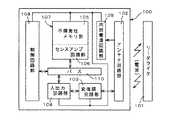
図1は、本発明の実施の形態1におけるICカードの例を示した概略のブロック図である。
【0018】
図1において、非接触型のICカード(以下、単にICカードと呼ぶ)1は、データ読み出し/書き込み装置(以下、リーダライタと呼ぶ)2との間で電波の授受を行うアンテナ回路部3と、データの変復調を行う変復調回路部4と、シリアルデータをパラレルデータに変換すると共にパラレルデータをシリアルデータに変換する入出力回路部5と、E2PROMで形成された不揮発性メモリ部6とセンスアンプ回路部7を備えたメモリ回路部8とを備えている。
【0019】
更に、ICカード1は、センスアンプ回路部7が不揮発性メモリ部6からのデータ読み出しが完了したか否かの検出を行う読み出し完了検出部9と、入出力回路部5及びメモリ回路部8の制御を行う制御回路部10と、アンテナ回路部3で受信した電波を整流して各回路部に電源として供給する内部電源回路部11と、入出力回路部5、メモリ回路部8、読み出し完了検出部9及び制御回路部10を接続するバス12とを備えている。なお、アンテナ回路部3、変復調回路部4及び入出力回路部5はインタフェース部をなし、不揮発性メモリ部6はメモリ部をなす。
【0020】
アンテナ回路部3は、変復調回路部4及び内部電源回路部11にそれぞれ接続され、変復調回路部4は、入出力回路部5に接続されている。また、入出力回路部5、メモリ回路部8、読み出し完了検出部9及び制御回路部10はバス12で接続され、内部電源回路部11は、変復調回路部4、入出力回路部5、メモリ回路部8、読み出し完了検出部9及び制御回路部10にそれぞれ接続されている。
【0021】
このような構成において、リーダライタ2は、常時、電波を発信しており、アンテナ回路部3は、リーダライタ2からの電波を受信し、該受信した電波を電気信号に変換して変復調回路部4及び内部電源回路部11に出力する。内部電源回路部11は、入力された電気信号の整流を行い各回路部に出力して電源供給を行う。リーダライタ2は、ICカード1にデータを送信しない場合は、無変調の電波を発信しており、データを送信する場合、該データを搬送波に変調させて含ませた電波を発信する。
【0022】
リーダライタ2からICカード1にデータが送信された場合、変復調回路部4は、アンテナ回路部3から入力された電気信号の復調を行ってデータの抽出を行い、抽出したデータを入出力回路部5に出力する。入出力回路部5は、変復調回路部4から入力されたシリアルデータをパラレルデータに変換してバス12に出力する。制御回路部10は、リーダライタ2から発信されたコマンドに従って動作し、メモリ回路部8の動作制御を行う。
【0023】
また、メモリ回路部8に格納されたデータをリーダライタ2に送信する場合、制御回路部10は、メモリ回路部8に対して所望のデータの読み出し動作を行わせ、該読み出しを行ったデータをバス12を介して入出力回路部5にパラレルデータで出力し、入出力回路部5は入力されたパラレルデータをシリアルデータに変換して変復調回路部4に出力する。変復調回路部4は、入力されたシリアルデータを搬送波に変調させて含ませる変調動作を行った後、該変調した信号をアンテナ回路部3に出力し、アンテナ回路部3は、入力された変調信号を電波にして送信する。
【0024】
次に、図2は、センスアンプ回路部7及び読み出し完了検出部9の例を示した回路図である。なお、図2では、複数あるセンスアンプの内の1つを示している。図2において、センスアンプ回路部7は、pチャネル型MOSトランジスタ(以下、pMOSトランジスタと呼ぶ)21〜23、nチャネル型MOSトランジスタ(以下、nMOSトランジスタと呼ぶ)24〜29、インバータ回路30,31及びコンデンサ32で形成されたセンスアンプ20を有している。また、読み出し完了検出部9は、センスアンプ回路部7の各センスアンプに対応する2入力のOR回路をそれぞれ有しており、図2では、センスアンプ20に対応する2入力のOR回路40を示している。
【0025】
センスアンプ20において、pMOSトランジスタ21及びnMOSトランジスタ24でインバータ回路33が形成され、pMOSトランジスタ22及びnMOSトランジスタ25でインバータ回路34が形成されている。インバータ回路33において、pMOSトランジスタ21及びnMOSトランジスタ24の各ドレインは接続されて出力をなすと共に、pMOSトランジスタ21及びnMOSトランジスタ24の各ゲートは接続されて入力をなし、nMOSトランジスタ24のソースは接地されている。同様に、インバータ回路34において、pMOSトランジスタ22及びnMOSトランジスタ25の各ドレインは接続されて出力をなすと共に、pMOSトランジスタ22及びnMOSトランジスタ25の各ゲートは接続されて入力をなし、nMOSトランジスタ25のソースは接地されている。
【0026】
インバータ回路33の出力はインバータ回路34の入力に接続されて該接続部をaとすると共に、インバータ回路33の入力はインバータ回路34の出力に接続されて該接続部をbとし、インバータ回路33及び34で差動増幅器35を形成している。pMOSトランジスタ21及び22の各ソースは、それぞれpMOSトランジスタ23のドレインに接続され、pMOSトランジスタ23のソースは電源端子VDDに接続されている。また、データの読み出し時に制御回路部10から「H」レベルの信号が入力される駆動信号入力端子36は、インバータ回路30を介してpMOSトランジスタ23、nMOSトランジスタ26及び27の各ゲートに接続されると共に、nMOSトランジスタ28及び29の各ゲートにそれぞれ接続されている。
【0027】
nMOSトランジスタ26及び28の各ドレインは、接続部aに接続されており、nMOSトランジスタ26のソースは接地されている。nMOSトランジスタ28のソースはデータ入力端子37を介して不揮発性メモリ部6のビット線45に接続されると共に、不揮発性メモリ部6においてビット線45にはE2PROMの多数のメモリセルに接続されているが、ここでは、その中の1つであるメモリセル46を代表して示している。メモリセル46のドレインはビット線45に接続され、メモリセル46のソースは接地され、ビット線45には、寄生容量47が存在している。
【0028】
また、nMOSトランジスタ27及び29の各ドレインは、接続部bに接続されており、nMOSトランジスタ27のソースは接地され、nMOSトランジスタ29のソースはコンデンサ32を介して接地されている。更に、接続部aは、読み出し完了検出部9におけるOR回路40の一方の入力に接続され、接続部bは、OR回路40の他方の入力に接続されると共にインバータ回路31の入力に接続され、インバータ回路31の出力は出力端子38に接続され、該出力端子38はセンスアンプ20の出力をなすと共にセンスアンプ回路部7の出力をなす。また、OR回路40の出力は読み出し完了検出部9の出力をなし、バス12を介して制御回路部10に接続されている。
【0029】
次に、センスアンプ回路部7の動作を説明する。制御回路部10は、センスアンプ回路部7を動作させないとき、駆動信号入力端子36に「L」レベルの信号を出力しており、pMOSトランジスタ23はオフすると共に、nMOSトランジスタ26及び27はオンすることから、接続部a及びbは共に「L」レベルとなる。このため、読み出し完了検出部9におけるOR回路40の出力は「L」レベルとなる。次に、駆動信号入力端子36に「H」レベルの信号が入力されると、nMOSトランジスタ26及び27がオフすることから、接続部a及びbは共にフローティング状態となる。更に、pMOSトランジスタ23、nMOSトランジスタ28及び29がオンすることから、pMOSトランジスタ21及び22がオンして、コンデンサ32及び寄生容量47への充電が始まる。
【0030】
ここで、メモリセル46のフローティングゲートに電荷が存在している場合、すなわち、メモリセル46に「L」レベルのデータが格納されている場合、データ入力端子37に接続されている選択されたメモリセル46にメモリセル電流Ieが流れることから、メモリセル46は導通状態となる。このため、寄生容量47を充電する速さよりもコンデンサ32を充電する速さの方が速く、コンデンサ32の充電完了時に、接続部bが先に「H」レベルとなることから、pMOSトランジスタ21がオフすると共にnMOSトランジスタ24がオンする。
【0031】
この結果、接続部aが「L」レベルに固定されることから、pMOSトランジスタ22がオンしnMOSトランジスタ25がオフして、接続部bは「H」レベルに固定される。接続部aが「L」レベルに固定されると共に、接続部bが「H」レベルに固定されることから、読み出し完了検出部9におけるOR回路40の出力は「H」レベルとなり、出力端子38は「L」レベルとなる。
【0032】
次に、メモリセル46のフローティングゲートに電荷が存在していない場合、すなわち、メモリセル46に「H」レベルのデータが格納されている場合、データ入力端子37に接続されている選択されたメモリセル46にメモリセル電流Ieが流れないことから、メモリセル46は非導通状態となる。更に、寄生容量47よりもコンデンサ32の容量の方が大きいため、コンデンサ32を充電する速さよりも寄生容量47を充電する速さの方が速く、寄生容量47の充電完了時に、接続部aが先に「H」レベルとなることから、pMOSトランジスタ22がオフすると共にnMOSトランジスタ25がオンする。
【0033】
この結果、接続部bが「L」レベルに固定されることから、pMOSトランジスタ21がオンしnMOSトランジスタ24がオフし、接続部aは「H」レベルに固定される。接続部aが「H」レベルに固定されると共に、接続部bが「L」レベルに固定されることから、読み出し完了検出部9のOR回路40の出力は「H」レベルとなり、出力端子38は「H」レベルとなる。
【0034】
これらのことから、不揮発性メモリ部6に格納されているデータを読み出す場合、制御回路部10によって駆動信号入力端子36が「H」レベルとなり、メモリセル46に格納されたデータが出力端子38から読み出されると共に、読み出し完了検出部9のOR回路40の出力が「H」レベルとなって、読み出しが完了したことを示し、該「H」レベルの信号が読み出し完了信号をなす。また、OR回路40の出力が「L」レベルの時は、読み出しが完了していないことを示している。制御回路部10は、読み出し完了検出部9におけるOR回路40の出力レベルによってセンスアンプ回路部7によるデータの読み出しが完了したか否かを判定する。
【0035】
ここで、図3は、ICカード1とリーダライタ2との間で行われるデータ授受の例を示した図である。図3において、ICカード1からデータを読み出す場合、リーダライタ2は、リードコマンドRCMDの後にパスワードを付加したデータをICカード1に送信する。ICカード1は、リーダライタ2から送信されたパスワードとあらかじめ不揮発性メモリ部6に格納されたパスワードとの照合を行い、一致するとリードコマンドRCMDを実行して不揮発性メモリ部6から読み出したデータをリーダライタ2に送信する。
【0036】
次に、ICカード1にデータを書き込む場合、リーダライタ2は、ライトコマンドWCMDの後にパスワードを付加し、更にパスワードの後に書き込むデ−タを付加したデータをICカード1に送信する。ICカード1は、リーダライタ2から送信されたパスワードとあらかじめ不揮発性メモリ部6に格納されたパスワードとの照合を行い、一致するとライトコマンドWCMDを実行してリーダライタ2から送信された書き込みデータを不揮発性メモリ部6に書き込んだ後、リーダライタ2に書き込み完了信号を出力する。
【0037】
このように、リーダライタ2は、ICカード1に対する読み出し及び書き込みのコマンドを送信する場合、該コマンドの後に必ずパスワードを付加して送信し、ICカード1は、リーダライタ2から送信されてきたパスワードが不揮発性メモリ部6内に格納されたパスワードと一致したときのみ、リーダライタ2からのコマンドに従って、不揮発性メモリ部6からのデータの読み出し及び書き込みを行う。上記パスワ−ドの照合は制御回路部10内に設けられたパスワード照合部50で行われる。
【0038】
図4は、パスワード照合部50の例を示した概略の回路図である。なお、図4では、不揮発性メモリ部6が8ビット構成の場合を例にして示している。
図4において、パスワード照合部50は、パスワード照合回路51〜58と8入力のOR回路59で形成されており、各パスワード照合回路51〜58の構成はそれぞれ同じであるので、パスワード照合回路51を例にして説明する。なお、図4ではパスワード照合回路53〜56を省略している。パスワード照合回路51は、比較回路61、2入力のOR回路62,63及びDフリップフロップ64で形成されている。
【0039】
OR回路62は、一方の入力が反転入力となっており、他方の入力が非反転入力となっている。OR回路62の反転入力は、センスアンプ回路部7におけるOR回路40の出力に接続され、非反転入力は、比較回路61の出力に接続されている。OR回路63において、一方の入力はOR回路62の出力に、他方の入力はDフリップフロップ64の非反転出力Qに、出力はDフリップフロップ64のD入力にそれぞれ接続されている。
【0040】
また、Dフリップフロップ64のクロックパルス入力Tは反転入力になっており、不揮発性メモリ部6からデータの読み出しを行っていることを示す、例えばここではデータの読み出しを行っている間は「H」レベルとなり、それ以外は「L」レベルとなる読み出し信号が制御回路部10によって入力される。Dフリップフロップ64のリセット入力Rにおいても反転入力になっており、パスワードの比較を行っている間、「H」レベルの信号が制御回路部10によって入力され、Dフリップフロップ64の非反転出力QはOR回路59の入力の1つに接続されている。なお、図4において、OR回路62の反転入力に入力される信号をeとし、Dフリップフロップ64において、クロックパルス入力Tに入力される信号をfとし、リセット入力Rに入力される信号をgとし、OR回路59から出力される信号をhとして示している。
【0041】
比較回路61の一方の入力には、不揮発性メモリ部6から読み出されたパスワードを形成する1ビットのデータが入力され、比較回路61の他方の入力にはリーダライタ2から送信されたパスワードを形成する1ビットのデータが入力される。例えば、不揮発性メモリ部6から読み出されたパスワードが8ビットのデータD0〜D7で形成され、該データD0〜D7に対応するリーダライタ2から入力されたパスワードの8ビットデータをDa0〜Da7とすると、比較回路61の一方の入力には1ビットデータD0が入力され、比較回路61の他方の入力には1ビットデータDa0が入力される。比較回路61は、データD0とデータDa0との比較を行い、一致しなかった場合のみ出力から「H」レベルの不一致信号を出力し、その他のときは、出力が「L」レベルになる。
【0042】
図5は、パスワード照合回路51におけるパスワードが一致しているときの動作例を示したタイミングチャートであり、図5を参照しながらパスワード照合部50の動作を説明する。なお、図5では、不揮発性メモリ部6に格納されたパスワードをPWとし、リーダライタ2から入力されたパスワードをPWaとして示しており、パスワードPW及びPWaはそれぞれ複数のバイトデータからなり、、8ビットデータを1バイトデータとして示している。以下、パスワードPWの1バイト分のデータD0〜D7及び、パスワードPWaの1バイト分のデータDa0〜Da7を例にして説明する。
【0043】
センスアンプ回路部7によるデータの読み出しが完了した場合、読み出し完了検出部9におけるOR回路40の出力は「H」レベルとなり、OR回路62の反転入力に「H」レベルの信号が入力されることから、比較回路61による比較結果、すなわち比較回路61の出力レベルに応じてOR回路62の出力のレベルが変化する。比較回路61による比較の結果、一致した場合、比較回路61の出力は「L」レベルとなり、OR回路62の出力は「L」レベルとなる。
【0044】
ここで、パスワードの読み出しが行われて、クロックパルス入力Tが「H」レベルに立ち上がるとDフリップフロップ64の非反転出力Qは「L」レベルとなる。同様にして、パスワード照合回路52〜58の各比較回路によって1ビットデータD1〜D8とDa1〜Da8との比較が行われ、パスワード照合回路52〜58の各Dフリップフロップの非反転出力Qがすべて「L」レベルであれば、OR回路59の出力は「L」レベルとなり、照合エラーが発生せず正常であることを示し、制御回路部10は、リーダライタ2からパスワードと共に送信されてきたコマンドに従って動作する。
【0045】
また、比較回路61による比較結果が不一致であった場合、比較回路61の出力は「H」レベルとなり、OR回路62の出力は「H」レベルとなって、Dフリップフロップ64の非反転出力は「H」レベルとなる。この結果、OR回路59の出力は「H」レベルとなって照合エラーが発生したことを示す。このように、パスワード照合回路51〜58の各Dフリップフロップの非反転出力のいずれか1つでも「H」レベルである場合、OR回路59の出力は「H」レベルとなって照合エラーが発生したことを示す。
【0046】
このことから、制御回路部10は、所定の照合エラー処理、例えばパスワードと共に送信されてきた読み出し又は書き込み等のコマンドの実行を行わず、リーダライタ2に照合エラーが発生したことを示す所定の照合エラー信号をバス12に出力する。バス12に出力された照合エラー信号は、入出力回路部5でシリアルデータに変換された後、変復調回路部4で変調されてアンテナ回路部3から発信される。なお、所定の照合エラー処理として、リーダライタ2に照合エラー信号を出力せず、パスワードと共に送信されてきた読み出し又は書き込み等のコマンドの実行を行わずに、リーダライタ2からの新たなコマンドの送信を待つようにしてもよい。
【0047】
一方、センスアンプ回路部7によるデータの読み出しが完了していない場合、読み出し完了検出部9におけるOR回路40の出力は「L」レベルであり、OR回路62の反転入力に「L」レベルの信号が入力されることから、比較回路61の比較結果に関係なくOR回路62の出力は「H」レベルになり、OR回路63の出力も「H」レベルになって、Dフリップフロップ64の非反転出力Qは「H」レベルとなる。この結果、OR回路59の出力は「H」レベルとなって照合エラーが発生したことを示し、制御回路部10は、所定の照合エラー処理を行う。
【0048】
ここで、内部電源回路部11からの電源電圧が低下し、センスアンプ回路部7のみが動作を停止した状態において、制御回路部10がパスワードの照合を行うために不揮発性メモリ部6に格納されたパスワードを読み出す場合、制御回路部10から「H」レベルの信号が駆動信号入力端子36に入力され、nMOSトランジスタ28及び29が共にオンすることから、センスアンプ20の接続部a及びbはそれぞれ「L」レベルとなる。このため、読み出し完了検出部9におけるOR回路40の出力は「L」レベルとなって、読み出しが完了していないことを示しており、制御回路部10は、上記のようなパスワードが一致しなかったときと同じ照合エラー処理を行う。
【0049】
上記においては、制御回路部10は、照合エラー処理として、リーダライタ2からパスワードと共に送信されてきたコマンドの処理を行わず、次の新たなコマンドがリーダライタ2から送信されるのを待つコマンド待ちの状態になったが、照合エラー処理として制御回路部10の動作を停止させ、所定のリセット動作を行わない限り復帰しないようにしてもよい。このようにすることによって、ICカード1の不揮発性メモリ部6に対する外部からの不正なアクセスをより確実に防止することができ、ICカードのセキュリティ機能を更に高めることができる。
【0050】
また、OR回路59の出力信号を制御回路部10のリセット信号として使用してもよく、照合エラーが発生してOR回路59の出力が「H」レベルになると、制御回路部10にリセットがかかり、制御回路部10は、強制的に初期状態に戻ってコマンド待ちとなる。このようにすることによって、ICカード1がどのようにすると照合エラー処理が行われるかが分かり難くなり、ICカード1のセキュリティ機能を更に一層高めることができる。
【0051】
このように、本発明の実施の形態1におけるICカードは、制御回路部10によるパスワード照合時に、センスアンプ回路が動作していない状態、特に内部電源回路部11から供給される電源電圧低下によるセンスアンプ回路の動作停止状態を検出することができ、不揮発性メモリ部6にあらかじめ格納されたパスワードが、正常に読み出された否かを検出することができる。このことから、不揮発性メモリ部6にあらかじめ格納されたパスワードが、正常に読み出されていないことを検出すると、所定のエラー処理を行い不揮発性メモリ部6への不正なアクセスを防止することができる。このため、電源電圧の低下時にセンスアンプ回路部のみが動作しない状態における、不正なパスワードの照合が行われることを防止してICカードのセキュリティ機能を高めることができ、ICカードに格納されたデータの機密性を高めることができる。
【0052】
実施の形態2.
実施の形態1においては、内部電源回路部11から供給される電源電圧低下によるセンスアンプ回路部7のみが動作停止した状態において所定のエラー処理を行ってパスワードの照合が行われないようにした。しかし、制御回路部10の動作電源電圧の範囲がセンスアンプ回路部7よりも小さくなる、すなわち、制御回路部10の動作電源電圧の下限値がセンスアンプ回路部7よりも高くなるようにして、内部電源回路部11から供給される電源電圧が低下した場合、センスアンプ回路部7よりも先に制御回路部10が動作しないようにしてもよく、このようにしたものを本発明の実施の形態2とする。
【0053】
図6は、本発明の実施の形態2におけるICカードの例を示した概略のブロック図である。なお、図6において、図1と同じもの同じ符号で示しており、ここではその説明を省略すると共に、図1との相違点のみ説明する。
図6における図1との相違点は、図1の読み出し完了検出部9をなくし、図1の制御回路部10の回路構成を変えたことから図1の制御回路部10を制御回路部71とし、これらに伴って、図1のICカード1をICカード75としたことにある。
【0054】
図6において、ICカード75は、アンテナ回路部3と、変復調回路部4と、入出力回路部5と、不揮発性メモリ部6とセンスアンプ回路部7を備えたメモリ回路部8とを備えている。更に、ICカード75は、入出力回路部5及びメモリ回路部8の制御を行う制御回路部71と、内部電源回路部11と、入出力回路部5、メモリ回路部8及び制御回路部71を接続するバス12とを備えている。アンテナ回路部3は、変復調回路部4及び内部電源回路部11にそれぞれ接続され、変復調回路部4は、入出力回路部5に接続されている。また、入出力回路部5、メモリ回路部8及び制御回路部71はバス12で接続され、内部電源回路部11は、変復調回路部4、入出力回路部5、メモリ回路部8及び制御回路部71にそれぞれ接続されている。
【0055】
このような構成において、リーダライタ2からICカード1にデータが送信された場合、制御回路部71は、リーダライタ2から送信されたコマンドに従って動作し、メモリ回路部8の動作制御を行う。また、メモリ回路部8に格納されたデータをリーダライタ2に送信する場合、制御回路部71は、メモリ回路部8に対して所望のデータの読み出し動作を行わせ、該読み出しを行ったデータをバス12を介して入出力回路部5にパラレルデータで出力する。
【0056】
制御回路部71は、内部にクロック信号を生成して出力するクロック生成部81を備えており、該クロック生成部81で生成されたクロック信号を基にして動作している。クロック生成部81は、クロック信号を生成するクロック生成回路部82とバッファ回路部83とで形成されており、クロック生成回路部82で生成されたクロック信号はバッファ回路部83を介して制御回路部71内に出力される。クロック生成部81からクロック信号が出力されなくなると、制御回路部71は動作を停止する。
【0057】
ここで、制御回路部71の動作電源電圧の範囲はセンスアンプ回路部7よりも小さく、すなわち、制御回路部71は、動作電源電圧の下限値がセンスアンプ回路部7よりも高くなるように形成されている。具体的には、クロック生成部81におけるバッファ回路部83は、動作電源電圧の下限値をセンスアンプ回路部7よりも高くなるように形成されている。このようにすることによって、内部電源回路部11から供給される電源電圧が低下した場合、ICカード75内でバッファ回路部83が最も高い電源電圧で動作しなくなり、これに伴って、制御回路部71の動作が停止する。
【0058】
また、制御回路部71がマイコンで形成されている場合、該マイコンは、内蔵されたマスクROMに格納されているプログラムに従って動作する。従って、マイコンは、マスクROMが動作しなくなると動作を停止し、制御回路部71は動作を停止する。ここで、マイコンに内蔵されているマスクROMは、動作電源電圧の範囲がセンスアンプ回路部7よりも小さくなるように、すなわち、動作電源電圧の下限値をセンスアンプ回路部7よりも高くなるように形成されている。このようにすることによって、内部電源回路部11から供給される電源の電圧が低下した場合、ICカード75内でマスクROMが最も高い電源電圧で動作しなくなり、これに伴って、マイコンの動作が停止し制御回路部71の動作が停止する。
【0059】
このように、本発明の実施の形態2におけるICカードは、制御回路部71において、動作電源電圧の範囲を小さくして動作電源電圧の下限値がセンスアンプ回路部7よりも高くなるようにした。このことから、内部電源回路部11から供給される電源電圧低下時に、センスアンプ回路部7のみが動作停止状態になることをなくし、不正なパスワードの照合が行われないようにすることができる。このため、電源電圧の低下時にセンスアンプ回路部7のみが動作を停止し、不正なパスワードの照合が行われることを防止してICカードのセキュリティ機能を高めることができ、ICカードに格納されたデータの機密性を高めることができる。
【0060】
なお、上記実施の形態1及び実施の形態2においては、非接触型のICカードを例にして説明したが、本発明はこれに限定するものではなく、接触型のICカードにおいても適用することができる。接触型のICカードの場合、アンテナ回路部3をリーダライタ2に電気的に接続するためのコネクタに置き換え、変復調回路部4及び入出回路部5をリーダライタ2とのインタフェースを行うインタフェース回路部に置き換え、内部電源回路部11がなくリーダライタ2から直接電源が供給される以外は実施の形態1及び実施の形態2で示した非接触型のICカードと同様であるのでその説明を省略する。なお、このような接触型のICカードカードにおいては、上記コネクタ及びインタフェース回路部がインタフェース部をなす。
【0061】
【発明の効果】
第1の発明に係るICカードは、制御回路部によるパスワード照合時に、読み出し完了検出部によって、センスアンプ回路部が動作していない状態、特に電源電圧低下によるセンスアンプ回路部の動作停止状態を検出することができ、メモリ部にあらかじめ格納されたパスワードが、正常に読み出されたか否かを検出することができる。このことから、メモリ部にあらかじめ格納されたパスワードが、正常に読み出されていないことを検出すると、所定のエラー処理を行いメモリ部への不正なアクセスを防止することができる。このため、電源電圧の低下時にセンスアンプ回路部のみが動作しない状態における、不正なパスワードの照合が行われることを防止してICカードのセキュリティ機能を高めることができ、ICカードに格納されたデータの機密性を高めることができる。
具体的には、上記センスアンプ回路部の接続制御部は、上記メモリ部からのデータ読み出し停止時に、上記第1及び第2の各接続部を上記所定の電圧に接続してそれぞれ同じ論理レベルにし、上記メモリ部からデータを読み出す場合は、上記第1及び第2の各接続部に対する上記所定の電圧への接続を遮断すると共に、上記選択されたメモリセルに接続されたビット線の寄生容量の他端を上記第1の接続部に接続すると共に、上記コンデンサの他端を上記第2の接続部に接続し、上記選択されたメモリセルに接続されたビット線の寄生容量は上記第1のインバータ回路を介して充電されると共に、上記コンデンサは上記第2のインバータ回路を介して充電され、上記読み出し完了検出部は、上記第1及び第2の各接続部の論理レベルが異なる状態になると、所定の読み出し完了信号を出力する。このようにすることによって、制御回路部によるパスワード照合時に、センスアンプ回路部が動作していない状態、特に電源電圧低下によるセンスアンプ回路部の動作停止状態を検出することができ、メモリ部にあらかじめ格納されたパスワードが、正常に読み出された否かを検出することができる。このことから、メモリ部にあらかじめ格納されたパスワードが、正常に読み出されていないことを検出すると、所定のエラー処理を行いメモリ部への不正なアクセスを防止することができる。このため、電源電圧の低下時にセンスアンプ回路部のみが動作しない状態で、不正なパスワードの照合が行われることを防止してICカードのセキュリティ機能を高めることができ、ICカードに格納されたデータの機密性を高めることができる。
【0062】
第2の発明に係るICカードは、第1の発明において、具体的には、上記制御回路部は、読み出し完了検出部から読み出し完了信号が出力されない場合、動作を停止すると共に、所定の処理を行わない限り復帰しないようにした。このようにすることによって、ICカードのメモリ部に対する外部からの不正なアクセスをより確実に防止することができ、ICカードのセキュリティ機能を更に高めることができる。
【0063】
第3の発明に係るICカードは、第1の発明において、具体的には、上記制御回路部は、読み出し完了検出部から読み出し完了信号が出力されない場合、リセットをかけて初期状態に戻るようにした。このようにすることによって、ICカードがどのようにすると照合エラー処理が行われるかが分かり難くなり、ICカードのセキュリティ機能を更に一層高めることができる。
【0065】
第4の発明に係るICカードは、制御回路部における動作電源電圧の範囲を小さくして動作電源電圧の下限値がセンスアンプ回路部よりも高くなるようにした。このことから、電源電圧低下時に、センスアンプ回路部のみが動作停止状態になることをなくし、不正なパスワードの照合が行われないようにすることができる。このため、電源電圧の低下時にセンスアンプ回路部のみが動作を停止し、不正なパスワードの照合が行われることを防止してICカードのセキュリティ機能を高めることができ、ICカードに格納されたデータの機密性を高めることができる。
【0066】
第5の発明に係るICカードは、第4の発明において、具体的には、上記制御回路部は、クロック信号を生成するクロック生成部を備え、該クロック生成部で生成されたクロック信号を基にして動作し、クロック生成部は、上記センスアンプ回路部よりも動作電源電圧の下限値が高くなるように形成される。このようにすることによって、電源電圧低下時に、センスアンプ回路部のみが動作停止状態になることをなくし、不正なパスワードの照合が行われないようにすることができる。このため、電源電圧の低下時にセンスアンプ回路部のみが動作を停止し、不正なパスワードの照合が行われることを防止してICカードのセキュリティ機能を高めることができ、ICカードに格納されたデータの機密性を高めることができる。
【0067】
第6の発明に係るICカードは、第4の発明において、具体的には、上記制御回路部は、マスクROMを有するマイコンで形成されると共に、該マスクROMに格納されたプログラムに従って動作し、マスクROMは、上記センスアンプ回路部よりも動作電源電圧の下限値が高くなるように形成される。このようにすることによって、電源電圧低下時に、センスアンプ回路部のみが動作停止状態になることをなくし、不正なパスワードの照合が行われないようにすることができる。このため、電源電圧の低下時にセンスアンプ回路部のみが動作を停止し、不正なパスワードの照合が行われることを防止してICカードのセキュリティ機能を高めることができ、ICカードに格納されたデータの機密性を高めることができる。
【図面の簡単な説明】
【図1】 本発明の実施の形態1におけるICカードの例を示した概略のブロック図である。
【図2】 図1のセンスアンプ回路部7及び読み出し完了検出部9の例を示した回路図である。
【図3】 ICカード1とリーダライタ2との間で行われるデータ授受の例を示した図である。
【図4】 パスワード照合部50の例を示した概略の回路図である。
【図5】 図4のパスワード照合回路51におけるパスワードが一致しているときの動作例を示したタイミングチャートである。
【図6】 本発明の実施の形態2におけるICカードの例を示した概略のブロック図である。
【図7】 非接触型のICカードの従来例を示した概略のブロック図である。
【図8】 図7のセンスアンプ回路部106の例を示した回路図である。
【符号の説明】
1,75 ICカード、 2 リーダライタ、 3 アンテナ回路部、 4 変復調回路部、 5 入出力回路部、 6 不揮発性メモリ部、 7 センスアンプ回路部、 8 メモリ回路部、 9 読み出し完了検出部、 10,71 制御回路部、 11 内部電源回路部、 12 バス、 50 パスワード照合部、 51〜58 パスワード照合回路、 81 クロック生成部[0001]
BACKGROUND OF THE INVENTION
The present invention relates to an IC card that exchanges data with a data read / write device.
[0002]
[Prior art]
As an IC card for exchanging data with a data read / write device, a contact type IC card that is electrically connected to the data read / write device to exchange data, and data exchange with the data read / write device There has been a non-contact type IC card that uses a non-contact medium such as radio waves. FIG. 7 is a schematic block diagram showing an example of a conventional non-contact type IC card.
[0003]
In FIG. 7, a non-contact type IC card (hereinafter simply referred to as an IC card) 100 includes an
[0004]
FIG. 8 is a diagram showing a circuit example of the sense
[0005]
From this, a
[0006]
In the above configuration, the
[0007]
[Problems to be solved by the invention]
Here, the sense
[0008]
The power of the
[0009]
Such a problem does not occur only in the non-contact type IC card, and even in the contact type IC card, the power supply voltage supplied to the IC card is lowered and only the sense amplifier circuit unit in the memory unit does not operate. When it comes to the situation, the same problem occurs.
The present invention has been made to solve the above problems, and an object of the present invention is to obtain an IC card that can enhance the confidentiality of data stored in a memory.
[0010]
[Means for Solving the Problems]
The IC card according to the first aspect of the present invention is an IC card for exchanging data with a data reading / writing device.
An interface unit for interfacing with a data read / write device;
A memory unit that is formed of a plurality of memory cells and stores data;
A sense amplifier circuit unit for reading data of a selected memory cell of the memory unit;
A read completion detection unit that detects whether or not the sense amplifier circuit unit has completed reading data from the memory unit, and outputs a read completion signal indicating completion of reading when the completion of the data reading is detected; ,
The operation of the memory unit and the sense amplifier circuit unit is controlled in accordance with a command from the data read / write device input via the interface unit, and when the data stored in the memory unit is read, the read completion detection unit When a read completion signal is not output, a control circuit unit that performs predetermined error processing is provided.
The sense amplifier circuit section is
Different polarityTwoTransistors connected in series,For each transistorThe connection portion forms an output end and the control electrode of each transistor is connected to form an input end.One output is connected to the other inputFirst and second inverter circuits connected in a loop; and
A capacitor having one end connected to a predetermined voltage and a capacitance larger than the parasitic capacitance of the bit line connected to the selected memory cell;
With respect to the other end of the parasitic capacitance, one end of which is connected to the predetermined voltage, to the first connection portion that is a connection portion between the output end of the first inverter circuit and the input end of the second inverter circuit A connection for performing connection control and performing connection control to the second connection portion, which is a connection portion between the input terminal of the first inverter circuit and the output terminal of the second inverter circuit, with respect to the other end of the capacitor. A control unit;
With
When the data connection from the memory unit is stopped, the connection control unit connects the first and second connection units to the predetermined voltage to set the same logic level and reads data from the memory unit. The first and second connection portions are disconnected from the predetermined voltage, and the other end of the parasitic capacitance of the bit line connected to the selected memory cell is connected to the first connection portion. And connecting the other end of the capacitor to the second connection portion, and the parasitic capacitance of the bit line connected to the selected memory cell is charged via the first inverter circuit, The capacitor is charged via the second inverter circuit, and the read completion detection unit has a logic level of each of the first and second connection units.DifferentWhen the state is reached, a predetermined read completion signal is output.
[0011]
The IC card according to the second invention is the IC card according to the first invention, wherein the control circuit unit stops the operation when the read completion signal is not output from the read completion detection unit, and returns unless a predetermined process is performed. It is something that does not.
[0012]
In the IC card according to the third invention, in the first invention, the control circuit unit resets and returns to the initial state when no read completion signal is output from the read completion detection unit.
[0014]
Book number4The IC card according to the present invention is an IC card that exchanges data with a data reading / writing device.
An interface unit for interfacing with a data read / write device;
A memory unit that is formed of a plurality of memory cells and stores data;
A sense amplifier circuit unit for reading data of a selected memory cell of the memory unit;
A control circuit unit that controls the operation of the memory unit and the sense amplifier circuit unit according to a command from the data read / write device input via the interface unit,
The sense amplifier circuit section is
Two transistors with different polarities are connected in series, and the connection part of each transistor forms an output terminal and the control electrode of each transistor is connected to form an input terminal. One output terminal is connected to the other input terminal. Each of the first and second inverter circuits connected in a loop as described above,
A capacitor having one end connected to a predetermined voltage and a capacitance larger than the parasitic capacitance of the bit line connected to the selected memory cell;
With respect to the other end of the parasitic capacitance, one end of which is connected to the predetermined voltage, to the first connection portion that is a connection portion between the output end of the first inverter circuit and the input end of the second inverter circuit A connection for performing connection control and performing connection control to the second connection portion, which is a connection portion between the input terminal of the first inverter circuit and the output terminal of the second inverter circuit, with respect to the other end of the capacitor. A control unit;
With
When the data connection from the memory unit is stopped, the connection control unit connects the first and second connection units to the predetermined voltage to set the same logic level and reads data from the memory unit. The first and second connection portions are disconnected from the predetermined voltage, and the other end of the parasitic capacitance of the bit line connected to the selected memory cell is connected to the first connection portion. And connecting the other end of the capacitor to the second connection portion, and the parasitic capacitance of the bit line connected to the selected memory cell is charged via the first inverter circuit, The capacitor is charged via the second inverter circuit,The control circuit section is formed so that the lower limit value of the operating power supply voltage is higher than that of the sense amplifier circuit section.
[0015]
Book number5The IC card according to the invention is4In the invention, the control circuit unit includes a clock generation unit that generates a clock signal, and operates based on the clock signal generated by the clock generation unit. The clock generation unit is more than the sense amplifier circuit unit. It is formed so that the lower limit value of the operating power supply voltage is increased.
[0016]
Book number6The IC card according to the invention is4In the present invention, the control circuit section is formed by a microcomputer having a mask ROM and operates according to a program stored in the mask ROM. The mask ROM has a lower lower limit value of the operating power supply voltage than the sense amplifier circuit section. It is formed as follows.
[0017]
DETAILED DESCRIPTION OF THE INVENTION
Next, the present invention will be described in detail based on the embodiments shown in the drawings.
FIG. 1 is a schematic block diagram showing an example of an IC card according to
[0018]
In FIG. 1, a non-contact type IC card (hereinafter simply referred to as an IC card) 1 includes an antenna circuit unit 3 that exchanges radio waves with a data read / write device (hereinafter referred to as a reader / writer) 2. A modulation / demodulation circuit unit 4 for modulating / demodulating data, an input /
[0019]
Further, the
[0020]
The antenna circuit unit 3 is connected to the modulation / demodulation circuit unit 4 and the internal power supply circuit unit 11, and the modulation / demodulation circuit unit 4 is connected to the input /
[0021]
In such a configuration, the reader / writer 2 constantly transmits radio waves, and the antenna circuit unit 3 receives radio waves from the reader / writer 2 and converts the received radio waves into electrical signals to modulate / demodulate circuit units. 4 and the internal power supply circuit unit 11. The internal power supply circuit unit 11 rectifies the input electric signal and outputs it to each circuit unit to supply power. When the reader / writer 2 does not transmit data to the
[0022]
When data is transmitted from the reader / writer 2 to the
[0023]
Further, when data stored in the
[0024]
Next, FIG. 2 is a circuit diagram illustrating an example of the sense amplifier circuit unit 7 and the read completion detection unit 9. Note that FIG. 2 shows one of a plurality of sense amplifiers. 2, the sense amplifier circuit unit 7 includes p-channel MOS transistors (hereinafter referred to as pMOS transistors) 21 to 23, n-channel MOS transistors (hereinafter referred to as nMOS transistors) 24 to 29,
[0025]
In the
[0026]
The output of the
[0027]
The drains of the
[0028]
The drains of the
[0029]
Next, the operation of the sense amplifier circuit unit 7 will be described. When the control circuit unit 10 does not operate the sense amplifier circuit unit 7, it outputs an “L” level signal to the drive
[0030]
Here, when charge is present in the floating gate of the
[0031]
As a result, since the connection portion a is fixed at the “L” level, the
[0032]
Next, when there is no electric charge in the floating gate of the
[0033]
As a result, since the connection portion b is fixed at the “L” level, the
[0034]
Therefore, when reading data stored in the
[0035]
Here, FIG. 3 is a diagram showing an example of data exchange performed between the
[0036]
Next, when writing data to the
[0037]
As described above, when the reader / writer 2 transmits a read / write command to the
[0038]
FIG. 4 is a schematic circuit diagram showing an example of the
In FIG. 4, the
[0039]
OR
[0040]
Further, the clock pulse input T of the D flip-
[0041]
One input of the
[0042]
FIG. 5 is a timing chart showing an operation example when the passwords in the
[0043]
When the reading of data by the sense amplifier circuit unit 7 is completed, the reading completion detection unit 9OR circuitThe output of 40 becomes “H” level.OR circuitSince an “H” level signal is input to the inverting input of 62, the comparison result by the
[0044]
Here, when the password is read and the clock pulse input T rises to the “H” level, the non-inverted output Q of the D flip-
[0045]
If the comparison result by the
[0046]
Therefore, the control circuit unit 10 does not execute a predetermined verification error process, for example, a read or write command transmitted together with the password, and indicates that a verification error has occurred in the reader / writer 2. An error signal is output to the
[0047]
On the other hand, when the data read by the sense amplifier circuit unit 7 is not completed, the read completion detection unit 9OR circuitThe output of 40 is “L” level,OR circuitSince an “L” level signal is input to the inverting input of 62, the comparison result of the
[0048]
Here, in a state where the power supply voltage from the internal power supply circuit unit 11 has dropped and only the sense amplifier circuit unit 7 has stopped operating, the control circuit unit 10 is stored in the
[0049]
In the above, the control circuit unit 10 does not process the command transmitted with the password from the reader / writer 2 as the verification error process, but waits for the next new command to be transmitted from the reader / writer 2. However, the operation of the control circuit unit 10 may be stopped as a verification error process and may not be restored unless a predetermined reset operation is performed. By doing so, unauthorized access from the outside to the
[0050]
Also,OR circuit59 output signal may be used as a reset signal for the control circuit unit 10, and a collation error occurs.OR circuitWhen the output of 59 becomes “H” level, the control circuit unit 10 is reset, and the control circuit unit 10 forcibly returns to the initial state and waits for a command. By doing so, it becomes difficult to understand how the
[0051]
As described above, in the IC card according to the first embodiment of the present invention, when the password verification by the control circuit unit 10 is performed, the sense amplifier circuit is not operating, in particular, sensing due to a decrease in power supply voltage supplied from the internal power supply circuit unit 11. The operation stop state of the amplifier circuit can be detected, and it can be detected whether or not the password stored in advance in the
[0052]
Embodiment 2. FIG.
In the first embodiment, password verification is not performed by performing a predetermined error process in a state where only the sense amplifier circuit unit 7 is stopped due to a power supply voltage drop supplied from the internal power supply circuit unit 11. However, the range of the operating power supply voltage of the control circuit unit 10 is smaller than that of the sense amplifier circuit unit 7, that is, the lower limit value of the operating power supply voltage of the control circuit unit 10 is higher than that of the sense amplifier circuit unit 7, When the power supply voltage supplied from the internal power supply circuit unit 11 is lowered, the control circuit unit 10 may not be operated before the sense amplifier circuit unit 7, and this is the embodiment of the present invention. 2.
[0053]
FIG. 6 is a schematic block diagram showing an example of an IC card according to Embodiment 2 of the present invention. In FIG. 6, the same reference numerals as those in FIG. 1 are used, and the description thereof will be omitted here, and only differences from FIG. 1 will be described.
6 differs from FIG. 1 in that the read completion detection unit 9 in FIG. 1 is eliminated and the circuit configuration of the control circuit unit 10 in FIG. 1 is changed, so that the control circuit unit 10 in FIG. Accordingly, the
[0054]
In FIG. 6, an
[0055]
In such a configuration, when data is transmitted from the reader / writer 2 to the
[0056]
The
[0057]
Here, the range of the operating power supply voltage of the
[0058]
When the
[0059]
As described above, in the IC card according to the second embodiment of the present invention, in the
[0060]
In the first embodiment and the second embodiment, the non-contact type IC card has been described as an example. However, the present invention is not limited to this, and the present invention is also applicable to a contact type IC card. Can do. In the case of a contact type IC card, the antenna circuit unit 3 is replaced with a connector for electrically connecting to the reader / writer 2, and the modulation / demodulation circuit unit 4 and the input /
[0061]
【The invention's effect】
In the IC card according to the first aspect of the invention, when the password is verified by the control circuit unit, the read completion detection unit detects a state in which the sense amplifier circuit unit is not operating, particularly an operation stop state of the sense amplifier circuit unit due to a power supply voltage drop. The password stored in advance in the memory unit can be read successfullyOrWhether or not can be detected. From this, when it is detected that the password stored in advance in the memory unit is not normally read, predetermined error processing can be performed to prevent unauthorized access to the memory unit. For this reason, it is possible to improve the security function of the IC card by preventing unauthorized password verification in the state where only the sense amplifier circuit unit does not operate when the power supply voltage is lowered, and the data stored in the IC card Can increase confidentiality.
In particular,The connection control unit of the sense amplifier circuit unit connects the first and second connection units to the predetermined voltage when the data reading from the memory unit is stopped, and sets the same logic level. When reading data, the first and second connection portions are disconnected from the predetermined voltage, and the other end of the parasitic capacitance of the bit line connected to the selected memory cell is connected to the first connection portion. And the other end of the capacitor is connected to the second connection portion, and the parasitic capacitance of the bit line connected to the selected memory cell is connected via the first inverter circuit. When being charged, the capacitor is charged via the second inverter circuit, and the read completion detection unit is in a state where the logic levels of the first and second connection units are different. Outputs a predetermined read completion signal. By doing so, it is possible to detect a state in which the sense amplifier circuit unit is not operating, particularly an operation stop state of the sense amplifier circuit unit due to a power supply voltage drop, at the time of password verification by the control circuit unit. It is possible to detect whether or not the stored password has been successfully read. From this, when it is detected that the password stored in advance in the memory unit is not normally read, predetermined error processing can be performed to prevent unauthorized access to the memory unit. For this reason, it is possible to improve the security function of the IC card by preventing unauthorized password verification in the state where only the sense amplifier circuit unit does not operate when the power supply voltage is lowered, and the data stored in the IC card Can increase confidentiality.
[0062]
In the IC card according to the second invention, in the first invention, specifically, the control circuit unit stops the operation and performs predetermined processing when the read completion signal is not output from the read completion detection unit. It was made not to return unless it did. By doing so, unauthorized access from the outside to the memory unit of the IC card can be prevented more reliably, and the security function of the IC card can be further enhanced.
[0063]
In the IC card according to the third invention, in the first invention, specifically, the control circuit unit resets and returns to the initial state when the read completion signal is not output from the read completion detection unit. did. By doing so, it is difficult to understand how the IC card performs the verification error process, and the security function of the IC card can be further enhanced.
[0065]
First4In the IC card according to the present invention, the range of the operating power supply voltage in the control circuit section is reduced so that the lower limit value of the operating power supply voltage is higher than that in the sense amplifier circuit section. Therefore, when the power supply voltage is lowered, only the sense amplifier circuit unit is prevented from being stopped, and illegal password verification can be prevented. For this reason, only the sense amplifier circuit unit stops operating when the power supply voltage is lowered, and it is possible to improve the security function of the IC card by preventing unauthorized password verification, and the data stored in the IC card Can increase confidentiality.
[0066]
First5The IC card according to the invention is4Specifically, the control circuit unit includes a clock generation unit that generates a clock signal, and operates based on the clock signal generated by the clock generation unit. It is formed so that the lower limit value of the operating power supply voltage is higher than that of the amplifier circuit section. By doing so, it is possible to prevent only the sense amplifier circuit unit from being stopped when the power supply voltage is lowered, and to prevent unauthorized password verification. For this reason, only the sense amplifier circuit unit stops operating when the power supply voltage is lowered, and it is possible to improve the security function of the IC card by preventing unauthorized password verification, and the data stored in the IC card Can increase confidentiality.
[0067]
First6The IC card according to the invention is4Specifically, the control circuit unit is formed by a microcomputer having a mask ROM and operates according to a program stored in the mask ROM, and the mask ROM operates more than the sense amplifier circuit unit. It is formed so that the lower limit value of the power supply voltage is increased. By doing so, it is possible to prevent only the sense amplifier circuit unit from being stopped when the power supply voltage is lowered, and to prevent unauthorized password verification. For this reason, only the sense amplifier circuit unit stops operating when the power supply voltage is lowered, and it is possible to improve the security function of the IC card by preventing unauthorized password verification, and the data stored in the IC card Can increase confidentiality.
[Brief description of the drawings]
FIG. 1 is a schematic block diagram showing an example of an IC card in
2 is a circuit diagram illustrating an example of a sense amplifier circuit unit 7 and a read completion detection unit 9 in FIG. 1;
FIG. 3 is a diagram showing an example of data exchange performed between the
4 is a schematic circuit diagram showing an example of a
5 is a timing chart showing an operation example when passwords in the
FIG. 6 is a schematic block diagram showing an example of an IC card in Embodiment 2 of the present invention.
FIG. 7 is a schematic block diagram showing a conventional example of a non-contact type IC card.
8 is a circuit diagram illustrating an example of the sense
[Explanation of symbols]
1, 75 IC card, 2 reader / writer, 3 antenna circuit section, 4 modulation / demodulation circuit section, 5 input / output circuit section, 6 nonvolatile memory section, 7 sense amplifier circuit section, 8 memory circuit section, 9 read completion detection section, 10 , 71 control circuit unit, 11 internal power supply circuit unit, 12 bus, 50 password verification unit, 51-58 password verification circuit, 81 clock generation unit
Claims (6)
Translated fromJapaneseデータ読み出し/書き込み装置とのインタフェースを行うインタフェース部と、
複数のメモリセルで形成され、データを格納するメモリ部と、
該メモリ部の選択されたメモリセルのデータを読み出すセンスアンプ回路部と、
該センスアンプ回路部がメモリ部からのデータ読み出しを完了したか否かの検出を行い、該データ読み出しの完了を検出すると、読み出しが完了したことを示す読み出し完了信号を出力する読み出し完了検出部と、
上記インタフェース部を介して入力されるデータ読み出し/書き込み装置からのコマンドに従って、上記メモリ部及びセンスアンプ回路部の動作制御を行い、上記メモリ部に格納されたデータの読み出しに際して、読み出し完了検出部から読み出し完了信号が出力されない場合、所定のエラー処理を行う制御回路部とを備え、
上記センスアンプ回路部は、
極性の異なる2つのトランジスタが直列に接続され、該各トランジスタの接続部が出力端をなすと共に該各トランジスタの制御電極が接続されて入力端をなす、一方の出力端が他方の入力端に接続されるようにループ状に接続された第1及び第2の各インバータ回路と、
一端が所定の電圧に接続され、選択されたメモリセルに接続されたビット線の寄生容量よりも容量の大きいコンデンサと、
一端が上記所定の電圧に接続された上記寄生容量の他端に対して、第1のインバータ回路の出力端と第2のインバータ回路の入力端との接続部である第1の接続部への接続制御を行うと共に、上記コンデンサの他端に対して、第1のインバータ回路の入力端と第2のインバータ回路の出力端との接続部である第2の接続部への接続制御を行う接続制御部と、
を備え、
上記接続制御部は、上記メモリ部からのデータ読み出し停止時に、上記第1及び第2の各接続部を上記所定の電圧に接続してそれぞれ同じ論理レベルにし、上記メモリ部からデータを読み出す場合は、上記第1及び第2の各接続部に対する上記所定の電圧への接続を遮断すると共に、上記選択されたメモリセルに接続されたビット線の寄生容量の他端を上記第1の接続部に接続すると共に、上記コンデンサの他端を上記第2の接続部に接続し、上記選択されたメモリセルに接続されたビット線の寄生容量は上記第1のインバータ回路を介して充電されると共に、上記コンデンサは上記第2のインバータ回路を介して充電され、上記読み出し完了検出部は、上記第1及び第2の各接続部の論理レベルが異なる状態になると、所定の読み出し完了信号を出力することを特徴とするICカード。In an IC card that exchanges data with a data read / write device,
An interface unit for interfacing with a data read / write device;
A memory unit that is formed of a plurality of memory cells and stores data;
A sense amplifier circuit unit for reading data of a selected memory cell of the memory unit;
A read completion detection unit that detects whether or not the sense amplifier circuit unit has completed reading data from the memory unit, and outputs a read completion signal indicating completion of reading when the completion of the data reading is detected; ,
The operation of the memory unit and the sense amplifier circuit unit is controlled in accordance with a command from the data read / write device input via the interface unit, and when the data stored in the memory unit is read, the read completion detection unit When a read completion signal is not output, a control circuit unit that performs predetermined error processing is provided.
The sense amplifier circuit section is
Two transistors having different polarities are connected in series, forming an input end is connected to the control electrode of each of the transistors with connection portionsof therespective transistors constituting an output terminal,connected one output terminal to the other input terminal Each of the first and second inverter circuits connected in a loopas described above ,
A capacitor having one end connected to a predetermined voltage and a capacitance larger than the parasitic capacitance of the bit line connected to the selected memory cell;
With respect to the other end of the parasitic capacitance, one end of which is connected to the predetermined voltage, to the first connection portion that is a connection portion between the output end of the first inverter circuit and the input end of the second inverter circuit A connection for performing connection control and performing connection control to the second connection portion, which is a connection portion between the input terminal of the first inverter circuit and the output terminal of the second inverter circuit, with respect to the other end of the capacitor. A control unit;
With
When the data connection from the memory unit is stopped, the connection control unit connects the first and second connection units to the predetermined voltage to set the same logic level and reads data from the memory unit. The first and second connection portions are disconnected from the predetermined voltage, and the other end of the parasitic capacitance of the bit line connected to the selected memory cell is connected to the first connection portion. And connecting the other end of the capacitor to the second connection portion, and the parasitic capacitance of the bit line connected to the selected memory cell is charged via the first inverter circuit, the capacitor is charged through the second inverter circuit, the read completion detection unit, when the first and second logic levels of each connection part is adifferent state, complete predetermined read IC card and outputs the No..
データ読み出し/書き込み装置とのインタフェースを行うインタフェース部と、
複数のメモリセルで形成され、データを格納するメモリ部と、
該メモリ部の選択されたメモリセルのデータを読み出すセンスアンプ回路部と、
上記インタフェース部を介して入力されるデータ読み出し/書き込み装置からのコマンドに従って、上記メモリ部及びセンスアンプ回路部の動作制御を行う制御回路部とを備え、
上記センスアンプ回路部は、
極性の異なる2つのトランジスタが直列に接続され、該各トランジスタの接続部が出力端をなすと共に該各トランジスタの制御電極が接続されて入力端をなす、一方の出力端が他方の入力端に接続されるようにループ状に接続された第1及び第2の各インバータ回路と、
一端が所定の電圧に接続され、選択されたメモリセルに接続されたビット線の寄生容量よりも容量の大きいコンデンサと、
一端が上記所定の電圧に接続された上記寄生容量の他端に対して、第1のインバータ回路の出力端と第2のインバータ回路の入力端との接続部である第1の接続部への接続制御を行うと共に、上記コンデンサの他端に対して、第1のインバータ回路の入力端と第2のインバータ回路の出力端との接続部である第2の接続部への接続制御を行う接続制御部と、
を備え、
上記接続制御部は、上記メモリ部からのデータ読み出し停止時に、上記第1及び第2の各接続部を上記所定の電圧に接続してそれぞれ同じ論理レベルにし、上記メモリ部からデータを読み出す場合は、上記第1及び第2の各接続部に対する上記所定の電圧への接続を遮断すると共に、上記選択されたメモリセルに接続されたビット線の寄生容量の他端を上記第1の接続部に接続すると共に、上記コンデンサの他端を上記第2の接続部に接続し、上記選択されたメモリセルに接続されたビット線の寄生容量は上記第1のインバータ回路を介して充電されると共に、上記コンデンサは上記第2のインバータ回路を介して充電され、上記制御回路部は、センスアンプ回路部よりも動作電源電圧の下限値が高くなるように形成されることを特徴とするICカード。In an IC card that exchanges data with a data read / write device,
An interface unit for interfacing with a data read / write device;
A memory unit that is formed of a plurality of memory cells and stores data;
A sense amplifier circuit unit for reading data of a selected memory cell of the memory unit;
A control circuit unit that controls the operation of the memory unit and the sense amplifier circuit unit according to a command from the data read / write device input via the interface unit,
The sense amplifier circuit section is
Two transistors with different polarities are connected in series, and the connection part of each transistor forms an output terminal and the control electrode of each transistor is connected to form an input terminal. One output terminal is connected to the other input terminal. Each of the first and second inverter circuits connected in a loop as described above,
A capacitor having one end connected to a predetermined voltage and a capacitance larger than the parasitic capacitance of the bit line connected to the selected memory cell;
With respect to the other end of the parasitic capacitance, one end of which is connected to the predetermined voltage, to the first connection portion that is a connection portion between the output end of the first inverter circuit and the input end of the second inverter circuit A connection for performing connection control and performing connection control to the second connection portion, which is a connection portion between the input terminal of the first inverter circuit and the output terminal of the second inverter circuit, with respect to the other end of the capacitor. A control unit;
With
When the data connection from the memory unit is stopped, the connection control unit connects the first and second connection units to the predetermined voltage to set the same logic level and reads data from the memory unit. The first and second connection portions are disconnected from the predetermined voltage, and the other end of the parasitic capacitance of the bit line connected to the selected memory cell is connected to the first connection portion. And connecting the other end of the capacitor to the second connection portion, and the parasitic capacitance of the bit line connected to the selected memory cell is charged via the first inverter circuit, the capacitor is charged through the second inverter circuit, the control circuit unit, characterized in that it is formed as the lower limit value of the operating power supply voltage than the sense amplifier circuit portion is higher C card.
Priority Applications (5)
| Application Number | Priority Date | Filing Date | Title |
|---|---|---|---|
| JP11809497AJP3822707B2 (en) | 1997-05-08 | 1997-05-08 | IC card |
| KR1019970057287AKR100263395B1 (en) | 1997-05-08 | 1997-10-31 | IC card |
| US08/962,839US5896325A (en) | 1997-05-08 | 1997-11-03 | IC card with error processing unit for sense amplifiers |
| TW086117240ATW382107B (en) | 1997-05-08 | 1997-11-17 | IC card |
| CN97122966ACN1108588C (en) | 1997-05-08 | 1997-11-28 | IC card |
Applications Claiming Priority (1)
| Application Number | Priority Date | Filing Date | Title |
|---|---|---|---|
| JP11809497AJP3822707B2 (en) | 1997-05-08 | 1997-05-08 | IC card |
Publications (3)
| Publication Number | Publication Date |
|---|---|
| JPH10307896A JPH10307896A (en) | 1998-11-17 |
| JPH10307896A5 JPH10307896A5 (en) | 2004-12-16 |
| JP3822707B2true JP3822707B2 (en) | 2006-09-20 |
Family
ID=14727859
Family Applications (1)
| Application Number | Title | Priority Date | Filing Date |
|---|---|---|---|
| JP11809497AExpired - Fee RelatedJP3822707B2 (en) | 1997-05-08 | 1997-05-08 | IC card |
Country Status (5)
| Country | Link |
|---|---|
| US (1) | US5896325A (en) |
| JP (1) | JP3822707B2 (en) |
| KR (1) | KR100263395B1 (en) |
| CN (1) | CN1108588C (en) |
| TW (1) | TW382107B (en) |
Families Citing this family (21)
| Publication number | Priority date | Publication date | Assignee | Title |
|---|---|---|---|---|
| KR100473308B1 (en)* | 1995-01-31 | 2005-03-14 | 가부시끼가이샤 히다치 세이사꾸쇼 | Nonvolatile memory device |
| JP3667920B2 (en)* | 1997-02-21 | 2005-07-06 | ローム株式会社 | IC card |
| JP2000165375A (en) | 1998-11-30 | 2000-06-16 | Hitachi Ltd | Information processing device, IC card |
| US6618789B1 (en) | 1999-04-07 | 2003-09-09 | Sony Corporation | Security memory card compatible with secure and non-secure data processing systems |
| US6955299B1 (en)* | 1999-12-17 | 2005-10-18 | Centre For Wireless Communications Of National University Of Singapore | System and method for using a smart card |
| JP2001306316A (en)* | 2000-04-21 | 2001-11-02 | Sharp Corp | Control circuit and semiconductor device using the same |
| EP1158384B1 (en)* | 2000-05-22 | 2005-04-27 | Infineon Technologies AG | Security data processing unit and method therefor |
| US7185145B2 (en)* | 2001-06-04 | 2007-02-27 | Renesas Technology Corp. | Memory card |
| JP3898481B2 (en)* | 2001-10-03 | 2007-03-28 | 富士通株式会社 | Semiconductor memory device |
| JP4680918B2 (en) | 2003-05-30 | 2011-05-11 | プリヴァリス・インコーポレーテッド | System and method for assignment and use of media content subscription service privileges |
| US7267266B2 (en)* | 2003-07-10 | 2007-09-11 | Rouille David W | Security system |
| GB2427330A (en)* | 2003-12-08 | 2006-12-20 | Innovision Res & Tech Plc | Data storage devices |
| GB2413195A (en)* | 2004-04-17 | 2005-10-19 | Hewlett Packard Development Co | A memory tag and reader with password protection of tag memory |
| WO2006104354A1 (en) | 2005-03-30 | 2006-10-05 | Samsung Electronics Co., Ltd. | Rf-id tag reading system for using password and method thereof |
| WO2007145366A1 (en) | 2006-06-15 | 2007-12-21 | Kabushiki Kaisha Toshiba | Portable electronic device and control method thereof |
| RU2541846C2 (en) | 2008-12-15 | 2015-02-20 | Кардлаб Апс | Rfid tag |
| KR101042349B1 (en)* | 2008-12-22 | 2011-06-17 | 한국전자통신연구원 | Semiconductor chip with security function and its operation method |
| EP3035230A1 (en) | 2014-12-19 | 2016-06-22 | Cardlab ApS | A method and an assembly for generating a magnetic field |
| AU2015366215A1 (en) | 2014-12-19 | 2017-07-20 | Cardlab Aps | A method and an assembly for generating a magnetic field and a method of manufacturing an assembly |
| EP3082071A1 (en) | 2015-04-17 | 2016-10-19 | Cardlab ApS | Device for and method of outputting a magnetic field |
| EP4095728A1 (en) | 2021-05-26 | 2022-11-30 | Thales DIS France SA | Secure applet access protection |
Family Cites Families (3)
| Publication number | Priority date | Publication date | Assignee | Title |
|---|---|---|---|---|
| JP3083187B2 (en)* | 1991-09-30 | 2000-09-04 | 富士通株式会社 | Key management method of electronic wallet system |
| JPH0877787A (en)* | 1994-06-28 | 1996-03-22 | Matsushita Electric Ind Co Ltd | Semiconductor device |
| JPH08190799A (en)* | 1995-01-09 | 1996-07-23 | Mitsubishi Denki Semiconductor Software Kk | Sense amplifier circuit |
- 1997
- 1997-05-08JPJP11809497Apatent/JP3822707B2/ennot_activeExpired - Fee Related
- 1997-10-31KRKR1019970057287Apatent/KR100263395B1/ennot_activeExpired - Fee Related
- 1997-11-03USUS08/962,839patent/US5896325A/ennot_activeExpired - Lifetime
- 1997-11-17TWTW086117240Apatent/TW382107B/ennot_activeIP Right Cessation
- 1997-11-28CNCN97122966Apatent/CN1108588C/ennot_activeExpired - Fee Related
Also Published As
| Publication number | Publication date |
|---|---|
| KR100263395B1 (en) | 2000-08-01 |
| TW382107B (en) | 2000-02-11 |
| US5896325A (en) | 1999-04-20 |
| JPH10307896A (en) | 1998-11-17 |
| KR19980086408A (en) | 1998-12-05 |
| CN1199206A (en) | 1998-11-18 |
| CN1108588C (en) | 2003-05-14 |
Similar Documents
| Publication | Publication Date | Title |
|---|---|---|
| JP3822707B2 (en) | IC card | |
| US7377442B2 (en) | Multi-mode integrated circuit devices including mode detection and methods of operating the same | |
| CN104239265B (en) | storage device | |
| US6809952B2 (en) | Semiconductor integrated circuit, radio frequency identification transponder, and non-contact IC card | |
| KR100391876B1 (en) | Data storage media | |
| US7815110B2 (en) | Methods for controlling access to data stored in smart cards and related devices | |
| JP4124692B2 (en) | Nonvolatile semiconductor memory device | |
| JP2007317170A (en) | Ic module and cellular phone | |
| JPS62164187A (en) | Test program startup method | |
| CN213027505U (en) | Power package | |
| JP2000030475A (en) | Semiconductor memory device | |
| US7233525B2 (en) | Method of converting contents of flash memory cells in the presence of leakage | |
| CN1659659B (en) | Recovery device, method for a smart card and a data carrier | |
| JP4359346B2 (en) | Circuit and method for measuring negative threshold voltage of non-volatile memory cell | |
| JP3922501B2 (en) | Power supply device and card-like storage medium | |
| JP2004297779A (en) | Wireless communication IC and wireless communication information storage medium using the same | |
| US20110025472A1 (en) | Connection port system | |
| CN113539320B (en) | Storage units, storage devices and related identification labels | |
| CN100405074C (en) | Test terminal negation circuit | |
| US20100277281A1 (en) | Rfid tag and method for driving the same | |
| CN114503200B (en) | Method and system for reliable and secure memory erase | |
| CN213241208U (en) | NVM read-write equipment of non-contact IC card chip | |
| KR100734168B1 (en) | Secure data storage with memory card interface | |
| KR101061342B1 (en) | Connect port system | |
| JP2024064165A (en) | Electronic information storage medium, IC chip, non-contact IC card, processing method, and program |
Legal Events
| Date | Code | Title | Description |
|---|---|---|---|
| A521 | Request for written amendment filed | Free format text:JAPANESE INTERMEDIATE CODE: A523 Effective date:20040107 | |
| A621 | Written request for application examination | Free format text:JAPANESE INTERMEDIATE CODE: A621 Effective date:20040107 | |
| A977 | Report on retrieval | Free format text:JAPANESE INTERMEDIATE CODE: A971007 Effective date:20050905 | |
| A131 | Notification of reasons for refusal | Free format text:JAPANESE INTERMEDIATE CODE: A131 Effective date:20051011 | |
| A521 | Request for written amendment filed | Free format text:JAPANESE INTERMEDIATE CODE: A523 Effective date:20051129 | |
| A131 | Notification of reasons for refusal | Free format text:JAPANESE INTERMEDIATE CODE: A131 Effective date:20051227 | |
| A521 | Request for written amendment filed | Free format text:JAPANESE INTERMEDIATE CODE: A523 Effective date:20060223 | |
| A131 | Notification of reasons for refusal | Free format text:JAPANESE INTERMEDIATE CODE: A131 Effective date:20060425 | |
| A521 | Request for written amendment filed | Free format text:JAPANESE INTERMEDIATE CODE: A523 Effective date:20060523 | |
| TRDD | Decision of grant or rejection written | ||
| A01 | Written decision to grant a patent or to grant a registration (utility model) | Free format text:JAPANESE INTERMEDIATE CODE: A01 Effective date:20060620 | |
| A61 | First payment of annual fees (during grant procedure) | Free format text:JAPANESE INTERMEDIATE CODE: A61 Effective date:20060623 | |
| R150 | Certificate of patent or registration of utility model | Free format text:JAPANESE INTERMEDIATE CODE: R150 | |
| FPAY | Renewal fee payment (event date is renewal date of database) | Free format text:PAYMENT UNTIL: 20100630 Year of fee payment:4 | |
| FPAY | Renewal fee payment (event date is renewal date of database) | Free format text:PAYMENT UNTIL: 20110630 Year of fee payment:5 | |
| FPAY | Renewal fee payment (event date is renewal date of database) | Free format text:PAYMENT UNTIL: 20110630 Year of fee payment:5 | |
| S111 | Request for change of ownership or part of ownership | Free format text:JAPANESE INTERMEDIATE CODE: R313115 | |
| FPAY | Renewal fee payment (event date is renewal date of database) | Free format text:PAYMENT UNTIL: 20110630 Year of fee payment:5 | |
| R350 | Written notification of registration of transfer | Free format text:JAPANESE INTERMEDIATE CODE: R350 | |
| LAPS | Cancellation because of no payment of annual fees |