JP3822632B2 - Transmission circuit, reception circuit, clock extraction circuit, data transmission method and data transmission system - Google Patents
Transmission circuit, reception circuit, clock extraction circuit, data transmission method and data transmission systemDownload PDFInfo
- Publication number
- JP3822632B2 JP3822632B2JP2006515326AJP2006515326AJP3822632B2JP 3822632 B2JP3822632 B2JP 3822632B2JP 2006515326 AJP2006515326 AJP 2006515326AJP 2006515326 AJP2006515326 AJP 2006515326AJP 3822632 B2JP3822632 B2JP 3822632B2
- Authority
- JP
- Japan
- Prior art keywords
- circuit
- information
- data
- serial data
- signal
- Prior art date
- Legal status (The legal status is an assumption and is not a legal conclusion. Google has not performed a legal analysis and makes no representation as to the accuracy of the status listed.)
- Expired - Lifetime
Links
Images


Classifications
- H—ELECTRICITY
- H04—ELECTRIC COMMUNICATION TECHNIQUE
- H04L—TRANSMISSION OF DIGITAL INFORMATION, e.g. TELEGRAPHIC COMMUNICATION
- H04L25/00—Baseband systems
- H04L25/38—Synchronous or start-stop systems, e.g. for Baudot code
- H04L25/40—Transmitting circuits; Receiving circuits
- H04L25/49—Transmitting circuits; Receiving circuits using code conversion at the transmitter; using predistortion; using insertion of idle bits for obtaining a desired frequency spectrum; using three or more amplitude levels ; Baseband coding techniques specific to data transmission systems
- H—ELECTRICITY
- H04—ELECTRIC COMMUNICATION TECHNIQUE
- H04L—TRANSMISSION OF DIGITAL INFORMATION, e.g. TELEGRAPHIC COMMUNICATION
- H04L7/00—Arrangements for synchronising receiver with transmitter
- H04L7/02—Speed or phase control by the received code signals, the signals containing no special synchronisation information
- H04L7/033—Speed or phase control by the received code signals, the signals containing no special synchronisation information using the transitions of the received signal to control the phase of the synchronising-signal-generating means, e.g. using a phase-locked loop
- H—ELECTRICITY
- H03—ELECTRONIC CIRCUITRY
- H03L—AUTOMATIC CONTROL, STARTING, SYNCHRONISATION OR STABILISATION OF GENERATORS OF ELECTRONIC OSCILLATIONS OR PULSES
- H03L7/00—Automatic control of frequency or phase; Synchronisation
- H03L7/06—Automatic control of frequency or phase; Synchronisation using a reference signal applied to a frequency- or phase-locked loop
- H03L7/08—Details of the phase-locked loop
- H03L7/085—Details of the phase-locked loop concerning mainly the frequency- or phase-detection arrangement including the filtering or amplification of its output signal
- H03L7/087—Details of the phase-locked loop concerning mainly the frequency- or phase-detection arrangement including the filtering or amplification of its output signal using at least two phase detectors or a frequency and phase detector in the loop
- H—ELECTRICITY
- H03—ELECTRONIC CIRCUITRY
- H03L—AUTOMATIC CONTROL, STARTING, SYNCHRONISATION OR STABILISATION OF GENERATORS OF ELECTRONIC OSCILLATIONS OR PULSES
- H03L7/00—Automatic control of frequency or phase; Synchronisation
- H03L7/06—Automatic control of frequency or phase; Synchronisation using a reference signal applied to a frequency- or phase-locked loop
- H03L7/08—Details of the phase-locked loop
- H03L7/085—Details of the phase-locked loop concerning mainly the frequency- or phase-detection arrangement including the filtering or amplification of its output signal
- H03L7/091—Details of the phase-locked loop concerning mainly the frequency- or phase-detection arrangement including the filtering or amplification of its output signal the phase or frequency detector using a sampling device
- H—ELECTRICITY
- H03—ELECTRONIC CIRCUITRY
- H03L—AUTOMATIC CONTROL, STARTING, SYNCHRONISATION OR STABILISATION OF GENERATORS OF ELECTRONIC OSCILLATIONS OR PULSES
- H03L7/00—Automatic control of frequency or phase; Synchronisation
- H03L7/06—Automatic control of frequency or phase; Synchronisation using a reference signal applied to a frequency- or phase-locked loop
- H03L7/08—Details of the phase-locked loop
- H03L7/10—Details of the phase-locked loop for assuring initial synchronisation or for broadening the capture range
- H03L7/113—Details of the phase-locked loop for assuring initial synchronisation or for broadening the capture range using frequency discriminator
- H—ELECTRICITY
- H03—ELECTRONIC CIRCUITRY
- H03M—CODING; DECODING; CODE CONVERSION IN GENERAL
- H03M9/00—Parallel/series conversion or vice versa
- H—ELECTRICITY
- H04—ELECTRIC COMMUNICATION TECHNIQUE
- H04L—TRANSMISSION OF DIGITAL INFORMATION, e.g. TELEGRAPHIC COMMUNICATION
- H04L25/00—Baseband systems
- H04L25/38—Synchronous or start-stop systems, e.g. for Baudot code
- H04L25/40—Transmitting circuits; Receiving circuits
- H04L25/45—Transmitting circuits; Receiving circuits using electronic distributors
- H—ELECTRICITY
- H04—ELECTRIC COMMUNICATION TECHNIQUE
- H04L—TRANSMISSION OF DIGITAL INFORMATION, e.g. TELEGRAPHIC COMMUNICATION
- H04L25/00—Baseband systems
- H04L25/38—Synchronous or start-stop systems, e.g. for Baudot code
- H04L25/40—Transmitting circuits; Receiving circuits
- H04L25/49—Transmitting circuits; Receiving circuits using code conversion at the transmitter; using predistortion; using insertion of idle bits for obtaining a desired frequency spectrum; using three or more amplitude levels ; Baseband coding techniques specific to data transmission systems
- H04L25/4902—Pulse width modulation; Pulse position modulation
- H—ELECTRICITY
- H03—ELECTRONIC CIRCUITRY
- H03K—PULSE TECHNIQUE
- H03K7/00—Modulating pulses with a continuously-variable modulating signal
- H03K7/10—Combined modulation, e.g. rate modulation and amplitude modulation
Landscapes
- Engineering & Computer Science (AREA)
- Computer Networks & Wireless Communication (AREA)
- Signal Processing (AREA)
- Physics & Mathematics (AREA)
- Spectroscopy & Molecular Physics (AREA)
- Theoretical Computer Science (AREA)
- Dc Digital Transmission (AREA)
- Synchronisation In Digital Transmission Systems (AREA)
Description
Translated fromJapanese本発明は、パラレルなデジタルデータをシリアライズして伝送する送信回路および受信回路並びに送信回路に用いるエンコーダ回路、並びにそれらを用いたデータ伝送方法およびデータ伝送システムに関する。The present invention relates to a transmission circuit and a reception circuit for serializing and transmitting parallel digital data, an encoder circuit used for the transmission circuit, a data transmission method and a data transmission system using them.
また、本発明は、パラレルなデジタルデータをシリアライズして伝送されるシリアルデータ伝送システムの受信回路に関し、詳しくはシリアルデータ伝送システムの受信ユニットにおけるクロック復元位相同期回路(CDRPLL回路:Clock Data Recovery Phase Locked Loop回路、クロック抽出回路とも言う。)に関する。The present invention also relates to a receiving circuit of a serial data transmission system in which parallel digital data is serialized and transmitted, and more specifically, a clock recovery phase synchronization circuit (CDRPLL circuit: Clock Data Recovery Phase Locked) in a receiving unit of the serial data transmission system. Loop circuit and clock extraction circuit).
近年、装置間のデジタルデータの伝送においては、より高速にシリアル伝送を行いたいという要望が高まってきている。デジタルデータのシリアル伝送は、デジタルデータのパラレル伝送と比較して装置間を接続する配線を極力少なくすることができ、配線ケーブルおよびコネクタの小型化が図れるだけではなく、配線間の相互干渉によるクロストーク等を低減できる等の特徴がある。In recent years, there has been an increasing demand for serial transmission at higher speeds in digital data transmission between devices. Compared with parallel transmission of digital data, serial transmission of digital data can reduce the number of wirings connecting between devices as much as possible. Not only can the wiring cables and connectors be reduced in size, but also crosstalk due to mutual interference between the wirings. The feature is that talk and the like can be reduced.
一般に、デジタルデータのシリアル伝送において、送信ユニット側は、パラレルに供給されるデジタルデータをシリアルなデジタルデータに変換して受信ユニットへ送信する。一方、受信ユニット側では、受信したシリアルなデジタルデータをパラレルなデジタルデータへ復元する。In general, in serial transmission of digital data, the transmission unit side converts digital data supplied in parallel into serial digital data and transmits it to the reception unit. On the other hand, on the receiving unit side, the received serial digital data is restored to parallel digital data.
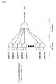
ここで、図65を参照する。図65は、パラレルなデジタルデータをシリアライズして伝送させるシリアルデータ伝送システムのシステム構成を示す図である。(1)電気/DC結合、(2)電気/AC結合、(3)光のいずれにおいても、送信ユニットに入力させるパラレルデータは、エンコーダで所定のエンコードされた後、シリアライザにおいてシリアルデータに変換され、増幅されて伝送される。受信ユニットで受信されたシリアルデータは、増幅された後CDRPLL回路でパラレルデータに変換され、デコーダでデコードされる。DC結合は簡易であると同時に、直流分を含めた低周波成分の伝送が可能であり、AC結合は、送信側と受信側とをDC的にアイソレーションできるメリットがある。光通信は、高速且つ長距離伝送が可能となるメリットがある。Reference is now made to FIG. FIG. 65 is a diagram showing a system configuration of a serial data transmission system that serializes and transmits parallel digital data. In any of (1) electrical / DC coupling, (2) electrical / AC coupling, and (3) light, parallel data to be input to the transmission unit is subjected to predetermined encoding by an encoder and then converted to serial data by a serializer. Amplified and transmitted. The serial data received by the receiving unit is amplified, converted to parallel data by the CDRPLL circuit, and decoded by the decoder. The DC coupling is simple, and at the same time, low frequency components including a direct current component can be transmitted. The AC coupling has an advantage that the transmission side and the reception side can be isolated in a DC manner. Optical communication has an advantage that high-speed and long-distance transmission is possible.
これらいずれの場合も、送信ユニット側および受信ユニット側でそれぞれ同期を取って復元動作が行われるが、同期が所定の範囲から逸脱すると正確なデジタルデータの復元はできなくなる。このため同期ずれが発生した場合は、同期の再調整が必要となる。特許文献1に、同期ずれが発生した場合、送信側に対し、コモンモードでリファレンスクロックの送信要求を送り、受信側で、要求したリファレンスクロックを受信すると位相比較モードから周波数比較モードへ切り替えて再調整するクロック復元回路の記載がある。In either of these cases, the restoration operation is performed by synchronizing on the transmission unit side and the reception unit side, respectively, but if the synchronization deviates from a predetermined range, accurate digital data cannot be restored. For this reason, when synchronization loss occurs, readjustment of synchronization is necessary. In
また、アクティブマトリクス型の液晶ディスプレイやプラズマディスプレイにおいて、デジタルデータはシリアル伝送されている(例えば、特許文献1参照)。ここで、この従来のシリアル伝送について図66および図67を参照しながら説明する。In active matrix liquid crystal displays and plasma displays, digital data is serially transmitted (see, for example, Patent Document 1). Here, this conventional serial transmission will be described with reference to FIGS. 66 and 67. FIG.
アクティブマトリクス型の液晶ディスプレイに用いられる画像データは、図66に示すように、RGBそれぞれの色データRx/Gx/BxとDE(DATA ENABLE)/Hsync(水平同期データ)/Vsync(垂直同期データ)からなる同期データとからなっている。画像データのソースからは、アクティブ期間には色データが出力され、ブランキング期間には同期データが出力される。なお、アクティブ期間即ちDE=“Hi”の期間においては、HsyncおよびVsyncは、“High”のままで変化しない。As shown in FIG. 66, the image data used in the active matrix type liquid crystal display is RGB color data Rx / Gx / Bx and DE (DATA ENABLE) / Hsync (horizontal synchronization data) / Vsync (vertical synchronization data). It consists of synchronous data consisting of From the source of image data, color data is output during the active period, and synchronous data is output during the blanking period. In the active period, that is, the period of DE = “Hi”, Hsync and Vsync remain “High” and do not change.
図67には、当該特許文献2に開示されているデジタルデータのシリアル伝送技術における、mビットの画像データをnビットのデータに符号化する方法の概略が示されている。この従来の符号化方法においては、同期データを送信しない場合(図67(A))と同期データを送信する場合(図67(B))とに場合分けして、mビットの画像データの符号化を行っている。FIG. 67 shows an outline of a method for encoding m-bit image data into n-bit data in the digital data serial transmission technique disclosed in
この従来の符号化において、同期データを送信しない場合(図67(A))は、画素毎のmビットの画像データを、同一論理ビットがk個以上連続しないnビットのシリアルな画像データに変換(encode)して時分割多重化して送信する。また、同期データを送信する場合(図67(B))は、画素毎のmビットの画像データを、時分割多重化し、同一論理ビットがk個連続した特定ビット列を含み(n−m)ビットでなる直列コードを付加することにより、シリアルな画像データに変換して時分割多重化して送信する。ここで、m、n、kは、それぞれ、m<n且つk<(n−m)という条件を満たしている。こうすることにより、パラレルに供給される画像データおよび同期データを送受信を中断させずに一つの伝送路によって送受信することができる。
ところが特許文献1の方法では、受信ユニット側にコモンモードドライバおよび送信側にコモンモード電圧検出回路を必要とするため、これらの付加回路の寄生容量、ノイズ等により伝送路の品質を下げる要因となる等の問題があった。またこの方法を光通信に応用する場合には、双方向の通信が必要なため、光ファイバを2本使うかWDM(波長多重)伝送を行う必要があり、いずれもコストアップの要因となる。However, since the method of
また、上述のような従来のシステムにおいては、送信ユニットと受信ユニットとの間ではトレーニング信号及びアクノレッジ信号を利用したシェイクハンド動作を行う必要があった。さらに、従来のシステムにおいて、受信ユニット側のCDRにおいて復元できるクロック周波数は一般に所定の狭い周波数範囲に限られていた。これは、受信ユニットのクロック抽出回路が、内蔵している水晶発振器や外部発振器からのクロック入力を基準クロックとして用いており、クロック抽出回路は、この基準クロックの近傍の周波数範囲のみしかクロックを抽出できないことによる。したがって、送信ユニット側からのシリアルデータの伝送レートが変化した場合は、受信側がクロック抽出できないためデータの復元ができないという問題があった。In the conventional system as described above, it is necessary to perform a shake hand operation using a training signal and an acknowledge signal between the transmission unit and the reception unit. Further, in the conventional system, the clock frequency that can be restored in the CDR on the receiving unit side is generally limited to a predetermined narrow frequency range. This is because the clock extraction circuit of the receiving unit uses the clock input from the built-in crystal oscillator or external oscillator as the reference clock, and the clock extraction circuit extracts the clock only in the frequency range near this reference clock. It can't be done. Therefore, when the transmission rate of serial data from the transmission unit side changes, there is a problem that data cannot be restored because the receiving side cannot extract the clock.
また、特許文献2に記載の符号化方法においては、以下に説明するとおり、シリアルデータをパラレルデータに変換する際のクロックの復元(抽出)におけるエラーの発生を十分に低減することはできなかった。In addition, in the encoding method described in
1シンボルのシリアルデータにライズエッジが複数存在すると、受信ユニット側でパラレル化する際、クロックの復元が元通りにできない可能性がある。ここで、1シンボルとは、入力されるデータと同周期またはその整数倍の周期のライズエッジもしくはフォールエッジで区切られているシリアルデータのブロックを言う。If there are a plurality of rise edges in one symbol of serial data, there is a possibility that the clock cannot be restored when parallelized on the receiving unit side. Here, one symbol refers to a block of serial data that is delimited by a rise edge or a fall edge having the same period as the input data or a period that is an integral multiple of the same period.
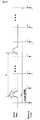
ここで、クロックの復元について説明する。図1に、1シンボルをデータA1、A2、A3・・・で構成するシリアルデータA(図1(A))および1シンボルをデータB1で構成するシリアルデータB(図1(B))から受信ユニット側においてクロックを復元するタイミングチャートを示す。図1(A)に示されるシリアルデータAには、1シンボル内に複数のライズエッジ(Rise Edge)およびフォールエッジ(Fall Edge)が存在する。一方、図1(B)に示されるシリアルデータBには、1シンボル内にライズエッジおよびフォールエッジがそれぞれ1つだけ存在する。Here, the clock restoration will be described. In FIG. 1, serial data A (FIG. 1 (A)) consisting of one symbol of data A1, A2, A3... 4 shows a timing chart for restoring a clock on the unit side. In the serial data A shown in FIG. 1A, a plurality of rise edges and fall edges exist within one symbol. On the other hand, the serial data B shown in FIG. 1B has only one rise edge and one fall edge in one symbol.
ここで、シリアルデータAからクロックを復元するために同期をとるタイミングをポイントA1即ちデータのライズエッジと設定した場合であっても、データの波形劣化やジッタ等の影響によりポイントA1でのクロック復元の同期がとれないことが起こり得る。すなわち、ポイントA1でのクロック復元の同期がとれない場合、ライズエッジであるポイントA2、A3等設定外のポイントにおいてクロックの復元の同期がとられてしまうことになり、正常なクロック復元ができなくなる。これは、シリアルデータAのように1シンボル内に複数のライズエッジが存在することにより起こり得るものである。Here, even when the timing to synchronize to restore the clock from the serial data A is set as the point A1, that is, the rise edge of the data, the clock restoration at the point A1 is caused by the influence of the waveform deterioration of the data, jitter, etc. May not be synchronized. That is, if the clock recovery at the point A1 cannot be synchronized, the clock recovery is synchronized at points other than the setting such as the points A2 and A3 which are rise edges, and normal clock recovery cannot be performed. . This can occur due to the presence of a plurality of rising edges in one symbol like the serial data A.
ここで、図2(A)および(B)を参照してより詳細に説明する。図2(A)に、デジタルデータC1〜C6を含むシリアルデータCを示す。一方、図2(B)に、シリアルデータCとはデータの構成が異なる、デジタルデータD1およびD2を含むシリアルデータDを示す。なお、ここでは、両シリアルデータの時間スケールは同じとする。Here, it demonstrates in detail with reference to FIG. 2 (A) and (B). FIG. 2A shows serial data C including digital data C1 to C6. On the other hand, FIG. 2B shows serial data D including digital data D1 and D2, which has a data configuration different from that of serial data C. Here, the time scale of both serial data is the same.
シリアルデータCにおけるデジタルデータC1〜C6、シリアルデータDにおけるデジタルデータD1およびD2において、C3のパルス幅とD1のパルス幅とを比較すると、C3に比べD1のパルス幅が長い。したがって、シリアルデータCのライズエッジおよびフォールエッジの数は、シリアルデータDのライズエッジよりも多くなっている。In the digital data C1 to C6 in the serial data C and the digital data D1 and D2 in the serial data D, the pulse width of D1 is longer than that of C3 when the pulse width of C3 is compared with the pulse width of D1. Therefore, the number of rise edges and fall edges of serial data C is larger than that of serial data D.
図2(A)に示すシリアルデータCにおける各デジタルデータC1〜C6の遷移近傍(ライズエッジまたはフォールエッジ近傍)では、デジタルデータの波形劣化、またはジッタ等の影響により、サンプリングエラーが発生する確率が高くなる。一方、図2(B)に示すシリアルデータDにおける各デジタルデータD1およびD2においては、それぞれのデータ長が比較的長く、データが同符号を持続する時間が比較的長いため、サンプリングエラーが発生する確率が非常に低くなる。言い換えると、シリアルデータのサンプリングエラーを低減するためには、デジタルデータのライズエッジが少なくなるようなデータ構成が望ましい。In the vicinity of the transition of each digital data C1 to C6 (near the rise edge or fall edge) in the serial data C shown in FIG. 2A, there is a probability that a sampling error will occur due to the waveform deterioration of the digital data or the influence of jitter. Get higher. On the other hand, in each of the digital data D1 and D2 in the serial data D shown in FIG. 2B, the data length is relatively long, and the time for which the data maintains the same sign is relatively long, so that a sampling error occurs. The probability is very low. In other words, in order to reduce serial data sampling errors, it is desirable to have a data configuration that reduces the rise edge of digital data.
本発明者らは、上述の従来から知られているシリアル伝送技術において、シリアルデータにライズエッジが1シンボル内に複数存在すると、ライズエッジをシンボルの区切りと誤認し、誤同期を起こすことがあり、このことがシリアルデータをパラレルデータに変換する際のクロックの復元におけるエラーの発生を十分に低減する障害となっていると考えた。In the above-described conventional serial transmission technology, the present inventors may misrecognize a rise edge as a symbol delimiter when a plurality of rise edges are present in one symbol and cause false synchronization. This is considered to be an obstacle to sufficiently reduce the occurrence of errors in clock recovery when converting serial data to parallel data.
図1(B)に示すような1シンボル内にライズエッジが1つしか存在しないシリアルデータBからクロックを復元する場合においては、クロックを復元するために同期をとるタイミングをポイントB1と設定すると、データの波形劣化やジッタ等の影響があっても、1シンボル内にライズエッジが1つしか存在しないので、クロックの復元にエラーが発生する可能性が低減される。In the case where the clock is restored from the serial data B in which only one rise edge exists in one symbol as shown in FIG. 1B, if the timing for synchronizing to restore the clock is set as point B1, Even if there is an influence of data waveform degradation, jitter, or the like, there is only one rise edge in one symbol, so the possibility of an error in clock recovery is reduced.
そこで、本発明は、上述の問題を鑑みてなされたものであり、受信ユニット側でリファレンスクロックを必要とせず且つシェイクハンド動作を必要としない簡易で高速なシリアルデータの伝送を行うことができるシリアルデータ伝送システムを提供するものである。また、本発明は、送信ユニット側のシリアルデータの伝送レートが変化しても受信ユニット側において、その変化に追随できるシリアルデータ伝送システムを提供するものである。Therefore, the present invention has been made in view of the above-described problems, and does not require a reference clock on the receiving unit side and can perform simple and high-speed serial data transmission that does not require a shake hand operation. A data transmission system is provided. The present invention also provides a serial data transmission system capable of following the change on the receiving unit side even if the transmission rate of serial data on the transmitting unit side changes.
また、本発明は、同期データをパルス幅変調することにより、シリアルデータ内のライズエッジを1つのみにし、クロックを復元する際のエラーを低減した信頼性の高いデジタルデータの伝送を実現することができるデータ伝送方法、その送信回路および受信回路並びにデータ伝送システムを提供するものである。In addition, the present invention realizes highly reliable digital data transmission by reducing the error when restoring the clock by using only one rising edge in the serial data by performing pulse width modulation on the synchronous data. A data transmission method, a transmission circuit and a reception circuit thereof, and a data transmission system are provided.
また、本発明は、受信ユニットの電圧制御発振回路の周波数をキャプチャレンジ内に入れるために、従来は必要であったリファレンスクロックを必要とせず、且つ双方向通信も必要としない、図65のいずれの構成においても適用可能な、クロック復元位相同期回路を提供することを目的とする。In addition, the present invention does not require a reference clock, which is necessary in the past, and does not require bidirectional communication in order to put the frequency of the voltage controlled oscillation circuit of the receiving unit within the capture range. An object of the present invention is to provide a clock recovery phase synchronization circuit that can be applied to the above configuration.
本発明は、第1の情報と第2の情報とをそれぞれ第1の期間と第2の期間とにおいて交互に周期的に伝送するデジタルデータ伝送方法であって、前記第1の期間における前記第1の情報の単位時間あたりの情報量は、前記第2の期間における前記第2の情報の単位時間あたりの情報量よりも多く、前記第1の期間における前記第1の情報は、最小のパルス幅のn倍を1シンボルとするシリアルデータとして伝送され、前記第2の期間における前記第2の情報は、パルス幅変調されたシリアルデータとして伝送されることを特徴とする。The present invention is a digital data transmission method for transmitting first information and second information alternately and periodically in a first period and a second period, respectively, wherein the first information and the second information are transmitted in the first period. The information amount per unit time of one information is larger than the information amount per unit time of the second information in the second period, and the first information in the first period is a minimum pulse. The second information is transmitted as serial data that is pulse-width-modulated, and is transmitted as serial data with n times the width as one symbol.
また、本発明は、第1の情報と第2の情報とをそれぞれ第1の期間と第2の期間とにおいて交互に周期的にシリアル伝送する伝送システムであって、前記第2の情報を、順にシリアル化して1シンボルのシリアルデータとしたときに前記第1の情報をシリアル化したときのシリアルデータの最小パルス幅のn倍の周期のパルス幅変調信号となるようにエンコードする第2のエンコーダと、前記第1の情報を、順にシリアル化したときの1シンボルのシリアルデータが前記パルス幅変調信号と相違するようにエンコードする第1のエンコーダと、前記エンコードされた前記第1の情報を前記1シンボルのシリアルデータに変換し、前記エンコードされた前記第2の情報を前記1シンボルの前記パルス幅変調信号であるシリアルデータに変換し、前記第1の情報の1シンボルシリアルデータと前記第2の情報の1シンボルシリアルデータとを交互に周期的にシリアル化するシリアル化回路と、前記シリアル化されたデータを伝送する伝送路と、前記伝送路を伝送した第1の情報のシリアルデータ又は前記第2の情報のシリアルデータからこれらシリアルデータにおける基準クロックを抽出するクロック抽出回路と、前記第1の情報のシリアルデータと前記第2の情報のシリアルデータとのデータの前記相違に基づき、前記第1の情報のシリアルデータと前記第2の情報のシリアルデータとを判別する情報判別回路と、前記分離された前記第1の情報のシリアルデータを前記第1のエンコーダに対応して前記第1の情報にデコードする第1のデコーダと、前記分離された前記第2の情報のシリアルデータを前記第2のエンコーダに対応して前記第2の情報にデコードする第2のデコーダと、を含み、前記第1の期間に伝送する前記第1の情報の単位時間当たりの情報量は、前記第2の期間に伝送する前記第2の情報の単位時間当たりの情報量よりも多いことを特徴とする。The present invention is also a transmission system for serially transmitting the first information and the second information alternately in the first period and the second period, respectively, wherein the second information is A second encoder that serially encodes the first information so that it becomes a pulse width modulation signal having a period of n times the minimum pulse width of the serial data when serializing the first information when serial data is made into one symbol. A first encoder that encodes serial data of one symbol when the first information is serialized differently from the pulse width modulation signal, and the encoded first information Converting into serial data of one symbol, converting the encoded second information into serial data that is the pulse width modulation signal of the one symbol, A serializing circuit that alternately and periodically serializes the 1-symbol serial data of the first information and the 1-symbol serial data of the second information; a transmission path for transmitting the serialized data; A clock extraction circuit for extracting a reference clock in the serial data from the serial data of the first information or the second data of the second information transmitted through the transmission line; the serial data of the first information; and the second information An information discriminating circuit for discriminating between the serial data of the first information and the serial data of the second information based on the difference between the serial data and the serial data of the first information; Corresponding to the first encoder, the first decoder for decoding the first information, and the separated second information A second decoder that decodes real data into the second information corresponding to the second encoder, and the amount of information per unit time of the first information transmitted in the first period is The amount of information per unit time of the second information transmitted in the second period is larger.
また、本発明は、第1の情報と第2の情報とをそれぞれ第1の期間と第2の期間とにおいて交互に周期的にシリアル伝送する伝送システムであって、前記第2の情報を、順にシリアル化して1シンボルのシリアルデータとしたときに前記第1の情報をシリアル化したときのシリアルデータの最小パルス幅のn倍の周期パルス幅変調信号となるようにエンコードする第2のエンコーダと、前記第1の情報を、順にシリアル化したときの1シンボルのシリアルデータが前記パルス幅変調信号と相違するようにエンコードする第1のエンコーダと、前記エンコードされた前記第1の情報を前記1シンボルのシリアルデジタルデータに変換し、前記エンコードされた前記第2の情報を前記1シンボルの前記パルス幅変調信号であるシリアルデータに変換し、前記第1の情報の1シンボルシリアルデータと前記第2の情報の1シンボルシリアルデータとを交互に周期的にシリアル化するシリアル化回路と、前記シリアル化されたデータを伝送する伝送路と、前記伝送路を伝送した第1の情報のシリアルデータ又は前記第2の情報のシリアルデータからこれらシリアルデータにおける基準クロックを抽出するクロック抽出回路と、を備え、前記クロック抽出回路は、電圧制御回路、前記シリアルデータと電圧制御発振回路の出力の位相を比較する位相比較回路、前記電圧制御回路の制御電圧を生成するループフィルタからなる位相比較ループと、前記シリアルデータを前記電圧制御発振回路で生成された多相クロックでサンプリングするサンプリング回路と、前記1シンボルのシリアルデータの周波数と前記電圧制御発振回路の発振周波数とを比較して、電圧制御発振回路の発振周波数を前記1シンボルのシリアルデータの周波数にあわせる周波数制御回路であって、前記電圧制御発振回路で作られた前記1シンボルの期間中のシリアル信号中のライズエッジの数が0か1かそれ以外か判定するエッジ数判定回路と、ライズエッジの数が0か、周波数制御回路がディゼイブルされた場合にリセットされ所定の時間間隔でタイマ信号を出力するタイマとを有し、ライズエッジの数が0の場合に電圧制御発振回路の発振周波数を下げ、タイマからタイマ信号が出力された場合には、電圧制御発振回路の周波数を上げるように制御を行う周波数制御回路と、前記周波数制御回路の出力を受けて、前記ループフィルタに電流パルスを出力するチャージポンプと、前記位相比較回路から周波数比較モード要求信号が入力された場合には、周波数制御回路をイネーブル、位相比較回路をディゼイブルし、ライズエッジもしくはフォールエッジの数が1の場合が所定の数以上続いたことを検出して、前記電圧制御発振回路の出力周波数が前記位相比較ループのキャプチャレンジ内であることを判定し、周波数制御回路をディゼイブル、位相比較回路をイネーブルするモード切り替え回路を有するクロック抽出回路と、前記第1の情報のシリアルデータと前記第2の情報のシリアルデータとのデータの前記相違に基づき、前記第1の情報のシリアルデータと前記第2の情報のシリアルデータとを識別する情報判別回路と、前記分離された前記第1の情報のシリアルデータを前記第1のエンコーダに対応して前記第1の情報にデコードする第1のデコーダと、前記分離された前記第2の情報のシリアルデータを前記第2のエンコーダに対応して前記第2の情報にデコードする第2のデコーダと、を含むことを特徴とする。The present invention is also a transmission system for serially transmitting the first information and the second information alternately in the first period and the second period, respectively, wherein the second information is A second encoder that serially encodes the first information so that it becomes a periodic pulse width modulation signal that is n times the minimum pulse width of the serial data when serializing the first information when serialized to one symbol; The first information is encoded such that serial data of one symbol when serialized in order is different from the pulse width modulation signal, and the encoded first information is the first information. The data is converted into serial digital data of symbols, and the encoded second information is converted into serial data which is the pulse width modulation signal of the one symbol. A serialization circuit that alternately and periodically serializes the 1-symbol serial data of the first information and the 1-symbol serial data of the second information; and a transmission path that transmits the serialized data; A clock extracting circuit for extracting a reference clock in the serial data from the serial data of the first information or the serial data of the second information transmitted through the transmission path, and the clock extracting circuit includes a voltage control circuit. A phase comparison circuit that compares the phase of the serial data and the output of the voltage controlled oscillation circuit, a phase comparison loop that includes a loop filter that generates a control voltage of the voltage control circuit, and the serial data is generated by the voltage controlled oscillation circuit A sampling circuit for sampling with the multi-phase clock, and the serial data of the one symbol A frequency control circuit that compares a wave number with an oscillation frequency of the voltage controlled oscillation circuit and adjusts the oscillation frequency of the voltage controlled oscillation circuit to the frequency of the serial data of the one symbol, and is made by the voltage controlled oscillation circuit This is reset when the number of rising edges in the serial signal during the period of one symbol is 0, 1 or not, and the number of rising edges is 0 or the frequency control circuit is disabled. And a timer that outputs a timer signal at a predetermined time interval. When the number of rise edges is 0, the oscillation frequency of the voltage controlled oscillation circuit is lowered, and when the timer signal is output from the timer, the voltage controlled oscillation is performed. A frequency control circuit that performs control to increase the frequency of the circuit, and a channel that receives an output of the frequency control circuit and outputs a current pulse to the loop filter. When the frequency comparison mode request signal is input from the stage pump and the phase comparison circuit, the frequency control circuit is enabled, the phase comparison circuit is disabled, and the number of rise edges or fall edges is 1 or more when a predetermined number A clock having a mode switching circuit that detects that the voltage control oscillation circuit detects that the output frequency is within the capture range of the phase comparison loop, disables the frequency control circuit, and enables the phase comparison circuit Based on the difference between the data of the extraction circuit and the serial data of the first information and the serial data of the second information, the serial data of the first information and the serial data of the second information are identified And an information discriminating circuit that performs serial data of the separated first information on the first encoder. Correspondingly, a first decoder that decodes the first information, and a second decoder that decodes the separated serial data of the second information into the second information corresponding to the second encoder. And a decoder.
また、本発明は、第1の情報と第2の情報とをそれぞれ第1の期間と第2の期間とにおいて交互に周期的にシリアル伝送するための送信回路であって、前記第2の情報を、順にシリアル化して1シンボルのシリアルデータとしたときに前記第1の情報をシリアル化したときのシリアルデータの最小パルス幅のn倍の周期のパルス幅変調信号となるようにエンコードする第2のエンコーダと、前記第1の情報を、順にシリアル化したときの1シンボルのシリアルデータが前記パルス幅変調信号と相違するようにエンコードする第1のエンコーダと、前記エンコードされた前記第1の情報を前記1シンボルのシリアルデータに変換し、前記エンコードされた前記第2の情報を前記1シンボルの前記パルス幅変調信号であるシリアルデータに変換するシリアル化回路と、を備える。Further, the present invention is a transmission circuit for serially transmitting the first information and the second information alternately in the first period and the second period, respectively, wherein the second information Are encoded so as to be a pulse width modulation signal having a cycle of n times the minimum pulse width of the serial data when the first information is serialized when serialized into serial data of one symbol. The encoder, the first encoder that encodes serial data of one symbol when the first information is serialized differently from the pulse width modulation signal, and the encoded first information. Is converted into serial data of one symbol, and the encoded second information is converted into serial data which is the pulse width modulation signal of the one symbol. Comprising a serial circuit, the.
また、前記第1のエンコーダは、前記1シンボルのシリアルデータ中に2つ以上のライズエッジを有するようにエンコードし、前記第2のエンコーダは、前記1シンボルのシリアルデータ中に1つのライズエッジのみを前記1シンボルの始点から一定位置に配されるようにエンコードするようにしてもよい。The first encoder encodes the serial data of one symbol so as to have two or more rising edges, and the second encoder encodes only one rising edge in the serial data of one symbol. May be encoded so as to be arranged at a fixed position from the starting point of the one symbol.
また、前記第1のエンコーダは、入力と出力との対応関係を複数有する組み合わせ論理回路と、少なくとも前記入力される第1の情報を評価し、この評価に基づいた判定信号を出力する判定回路とを備え、前記組み合わせ論理回路は、前記判定信号に応じて選択された前記対応関係のエンコードを行うとともに、この選択された前記対応関係を識別するためのエンコードビットを前記出力に付与するようにしてもよい。The first encoder includes a combinational logic circuit having a plurality of correspondences between inputs and outputs, a determination circuit that evaluates at least the input first information, and outputs a determination signal based on the evaluation. And the combinational logic circuit encodes the correspondence selected in accordance with the determination signal, and gives an encoded bit for identifying the selected correspondence to the output. Also good.
また、前記対応関係は、第1の対応関係と第2の対応関係とを含み、前記第1の対応関係は、前記入力と出力とが等しい関係であり、前記第2の対応関係は、前記入力に対して出力を2ビットおきに符号反転する関係であるようにしてもよい。In addition, the correspondence relationship includes a first correspondence relationship and a second correspondence relationship, and the first correspondence relationship is a relationship in which the input and the output are equal, and the second correspondence relationship is The relationship may be such that the output is inverted every two bits with respect to the input.
また、前記判定回路は、前記第1の情報を単純シリアル変換したときに、ライズエッジ数が0である場合には、前記組み合わせ論理回路に前記第2の対応関係を選択させる判定信号を出力する。The determination circuit outputs a determination signal for causing the combinational logic circuit to select the second correspondence when the number of rise edges is 0 when the first information is subjected to simple serial conversion. .
また、前記判定回路は、前記第1の情報を単純シリアル変換し、その前後に互いに符号の異なるスタートビットとストップビットとを付加したときに、ライズエッジ数が1である場合には、前記組み合わせ論理回路に前記第2の対応関係を選択させる判定信号を出力する。The determination circuit performs simple serial conversion on the first information, and adds a start bit and a stop bit having different signs before and after the first information. A determination signal for causing the logic circuit to select the second correspondence relationship is output.
また、前記判定回路は、前記組み合わせ論理回路に、前記複数の対応関係のうちエンコード後の前記1シンボルのシリアルデータにおける同符号連続数が、前記1シンボルのシリアルデータのビット数の2分の1に1を加えた値より小さくなる前記対応関係を選択させる判定信号を出力する。In addition, the determination circuit may cause the combinational logic circuit that the number of consecutive same-symbols in the serial data of one symbol after encoding among the plurality of correspondences is half of the number of bits of the serial data of one symbol. A determination signal for selecting the correspondence relationship that is smaller than a value obtained by adding 1 to is output.
また、前記判定回路は、前記組み合わせ論理回路に、前記複数の対応関係のうちエンコード後のデータの対称関係にあるデータのそれぞれの累積数の差を、最も小さくさせる前記対応関係を選択させる判定信号を出力する。In addition, the determination circuit causes the combinational logic circuit to select the correspondence relationship that minimizes the difference in the cumulative number of each of the plurality of correspondence relationships in the symmetrical relationship of the encoded data. Is output.
また、前記判定回路は、前記組み合わせ論理回路に、前記複数の対応関係のうちエンコード後のデータの対称関係にあるデータの累積数を、最も小さくさせる前記対応関係を選択させる判定信号を出力することを特徴とする。In addition, the determination circuit outputs a determination signal that causes the combinational logic circuit to select the correspondence relationship that minimizes the cumulative number of data in the symmetrical relationship of the encoded data among the plurality of correspondence relationships. It is characterized by.
また、前記判定回路は、主情報伝送周波数、EMI量、前記1シンボルのシリアルデジタルデータ及び前記パルス幅変調信号のSN比又はエラーレートのうち少なくとも一つを含む情報を評価し、その評価に応じた判定信号を出力するようにしてもよい。The determination circuit evaluates information including at least one of a main information transmission frequency, an EMI amount, the serial digital data of the one symbol, and an SN ratio or an error rate of the pulse width modulation signal, and according to the evaluation. The determination signal may be output.
また、前記ライズエッジをフォールエッジに置き換えても良い。The rise edge may be replaced with a fall edge.
また、前記第2のエンコーダは、前記第2の情報を、順にシリアル化したときに前記ライズエッジを始点とし、フォールエッジまでの同符号期間とするようにエンコードするようにしてもよい。The second encoder may encode the second information so that when the serialized information is sequentially serialized, the rising edge is the starting point and the same sign period is applied until the fall edge.
また、本発明は、第2の情報のシリアルデータであって、第1の情報の1シンボルのシリアルデータの最小パルス幅のn倍の周期のパルス幅変調信号である1シンボルのシリアルデータ化された第2の情報のシリアルデータと、第1の情報のシリアルデータであって、1シンボルのシリアルデータが前記パルス幅変調信号と相違するようにシリアル化された第1の情報のシリアルデータと、が交互に周期的にシリアル伝送された信号を受信するための受信回路であって、前記第1の情報のシリアルデータ又は前記第2の情報のシリアルデータからこれらシリアルデータにおける基準クロックを抽出するクロック抽出回路と、前記第1の情報のシリアルデータと前記第2の情報のシリアルデータとのデータの前記相違に基づき、前記第1の情報のシリアルデータと前記第2の情報のシリアルデータとを判別する情報判別回路と、前記判別された前記第1の情報のシリアルデータを前記第1のエンコーダに対応して前記第1の情報にデコードする第1のデコーダと、前記分離された前記第2の情報のシリアルデータを前記第2のエンコーダに対応して前記第2の情報にデコードする第2のデコーダと、を備えることを特徴とする。Also, the present invention converts the serial data of the second information into serial data of one symbol that is a pulse width modulation signal having a period n times as long as the minimum pulse width of the serial data of one symbol of the first information. Serial data of the second information, serial data of the first information, and serial data of the first information serialized so that one symbol of serial data is different from the pulse width modulation signal, Is a receiving circuit for receiving a signal periodically and alternately transmitted, and extracts a reference clock in the serial data of the first information or the serial data of the second information. Based on the difference between the extraction circuit and the serial data of the first information and the serial data of the second information, the first information An information discriminating circuit for discriminating serial data and serial data of the second information, and decoding the discriminated serial data of the first information into the first information corresponding to the first encoder A first decoder; and a second decoder that decodes the separated serial data of the second information into the second information corresponding to the second encoder.
また、前記第1の情報のシリアルデータは、エンコードモードを識別するエンコードビットを含み、前記第1のデコーダは、前記エンコードビットに応じたデコードを行う。The serial data of the first information includes an encode bit for identifying an encode mode, and the first decoder performs decoding according to the encode bit.
また、前記情報判別回路は、前記シリアルデータの1シンボル中におけるライズエッジ数に応じて前記第1の情報のシリアルデータと前記第2の情報のシリアルデータとを識別する。The information discriminating circuit discriminates between the serial data of the first information and the serial data of the second information according to the number of rising edges in one symbol of the serial data.
また、本発明は、第1のデジタルデータおよび第2のデジタルデータを1シンボルのシリアルデジタルデータに変換し受信回路へ送信するデジタルデータ送信回路であって、前記第2のデジタルデータを常に上位ビットの値が下位ビットの値以上であるデジタルデータにエンコードして前記1シンボルにライズエッジを1つのみ生成するエンコーダと、前記第1のデジタルデータ又は前記エンコードされた前記第2のデジタルデータを選択信号に基づき選択するスイッチ回路と、前記スイッチ回路の出力信号および前記選択信号をシリアルに変換するシリアル化回路と、を有する。According to another aspect of the present invention, there is provided a digital data transmission circuit for converting first digital data and second digital data into serial digital data of one symbol and transmitting the serial digital data to a receiving circuit, wherein the second digital data is always converted into upper bits. An encoder that encodes digital data whose value is equal to or greater than the value of the lower bits to generate only one rise edge in the one symbol, and selects the first digital data or the encoded second digital data A switch circuit that selects based on the signal; and a serialization circuit that converts the output signal of the switch circuit and the selection signal into serial.
また、本発明のデジタルデータ受信回路は、第1のシリアルデジタルデータを第1のデジタルデータおよび選択信号にパラレルに変換し、且つ1シンボルにライズエッジを1つだけ有する第2のシリアルデジタルデータを第2のデジタルデータおよび前記選択信号にパラレルに変換するパラレル化回路と、前記第2のデジタルデータをデコードし、第2のスイッチ回路へ出力するデコーダ回路と、前記第1のデジタルデータを前記選択信号に基づき選択し出力する第1のスイッチ回路と、前記デコードされた前記第2のデジタルデータを前記選択信号に基づき選択し出力する前記第2のスイッチ回路と、を有する。Also, the digital data receiving circuit of the present invention converts the first serial digital data into the first digital data and the selection signal in parallel, and the second serial digital data having only one rise edge per symbol. A parallel circuit for converting the second digital data and the selection signal into parallel, a decoder circuit for decoding the second digital data and outputting the second digital data to a second switch circuit, and the selection of the first digital data A first switch circuit that selects and outputs based on a signal; and the second switch circuit that selects and outputs the decoded second digital data based on the selection signal.
また、本発明は、第1のデジタルデータおよび第2のデジタルデータを1シンボルのシリアルデジタルデータに変換し受信回路へ送信するデジタルデータ送信回路であって、前記第1のデジタルデータをDCバランス処理して1シンボルに2以上のライズエッジを生成する第1のエンコーダと、前記第2のデジタルデータを常に上位ビットの値が下位ビットの値以上であるデジタルデータにエンコードして1シンボルにライズエッジを1つのみ生成する第2のエンコーダと、前記DCバランス処理された前記第1のデジタルデータ又は前記エンコードされた前記第2のデジタルデータを選択信号に基づき選択するスイッチ回路と、前記スイッチ回路の出力信号をシリアルに変換するシリアル化回路と、を有する。The present invention is also a digital data transmission circuit that converts the first digital data and the second digital data into serial digital data of one symbol and transmits the serial digital data to the reception circuit, and the first digital data is subjected to DC balance processing. A first encoder that generates two or more rise edges in one symbol, and the second digital data is always encoded into digital data in which the value of the upper bit is greater than or equal to the value of the lower bit, and the rise edge into one symbol A first encoder that generates only one of the first digital data that has been DC balanced, or a switch circuit that selects the encoded second digital data based on a selection signal; and And a serialization circuit for converting the output signal into serial.
また、本発明の受信回路は、1シンボルにライズエッジを2以上有する第1のシリアルデジタルデータを第1のデジタルデータにパラレルに変換し、且つ1シンボルにライズエッジを1つだけ有する第2のシリアルデジタルデータを第2のデジタルデータにパラレルに変換するパラレル化回路と、前記第1のデジタルデータをデコードし、第1のスイッチ回路へ出力する第1のデコーダ回路と、前記第2のデジタルデータをデコードし、第2のスイッチ回路へ出力するデコーダ回路と、前記第1のデジタルデータおよび前記第2のデジタルデータの前記ライズエッジの数を判定し、前記ライズエッジの数が1である場合と2以上である場合とで異なる選択信号を出力する判定回路と、前記デコードされた前記第1のデジタルデータを前記選択信号に基づき選択し出力する第1のスイッチ回路と、前記デコードされた前記第2のデジタルデータを前記選択信号に基づき選択し出力する前記第2のスイッチ回路と、を有する。The receiving circuit according to the present invention converts the first serial digital data having two or more rising edges in one symbol into parallel to the first digital data, and the second serial signal having only one rising edge in one symbol. A parallelizing circuit that converts serial digital data into second digital data in parallel; a first decoder circuit that decodes the first digital data and outputs the first digital data to a first switch circuit; and the second digital data When the number of rise edges of the first digital data and the second digital data is determined and the number of rise edges is 1, A determination circuit that outputs a selection signal that is different depending on whether the number is two or more, and the selection of the decoded first digital data Having a first switch circuit selects and outputs, based on the item, and a second switch circuit selects and outputs, based on the decoded second digital data and the selection signal.
また、本発明は、送信側ユニットにおいてパラレルに入力される第1のデジタルデータおよび第2のデジタルデータを1シンボルのシリアルデジタルデータに変換し、受信側ユニットへ送信するデジタルデータ伝送方法であって、第1の期間においては、前記第1のデジタルデータおよび選択信号を第1のシリアルデジタルデータに変換し前記受信側ユニットへ送信し、第2の期間においては、前記第2のデジタルデータを常に上位ビットの値が下位ビットの値以上であるようにエンコードして1シンボルにライズエッジを1つのみ生成し、且つ第2のシリアルデジタルデータに変換し前記受信側ユニットへ送信することを特徴とする。The present invention also relates to a digital data transmission method for converting first digital data and second digital data inputted in parallel in a transmission side unit into serial digital data of one symbol and transmitting the serial digital data to the reception side unit. In the first period, the first digital data and the selection signal are converted into first serial digital data and transmitted to the receiving unit, and in the second period, the second digital data is always transmitted. Encoding so that the value of the upper bit is greater than or equal to the value of the lower bit to generate only one rise edge in one symbol, converting it to second serial digital data, and transmitting it to the receiving side unit To do.
また、本発明は、送信側ユニットにおいてパラレルに入力される第1のデジタルデータおよび第2のデジタルデータを1シンボルのシリアルデジタルデータに変換し、受信側ユニットへ送信するデジタルデータ伝送方法であって、第1の期間においては、前記第1のデジタルデータをDCバランス処理し、前記DCバランス処理された前記第1のデジタルデータを第1のシリアルデジタルデータに変換し前記受信側ユニットへ送信し、第2の期間においては、前記第2のデジタルデータを常に上位ビットの値が下位ビットの値以上であるようにエンコードして1シンボルにライズエッジを1つのみ生成し、且つ第2のシリアルデジタルデータに変換し前記受信側ユニットへ送信することを特徴とする。The present invention also relates to a digital data transmission method for converting first digital data and second digital data inputted in parallel in a transmission side unit into serial digital data of one symbol and transmitting the serial digital data to the reception side unit. In the first period, the first digital data is subjected to DC balance processing, the first digital data subjected to the DC balance processing is converted into first serial digital data, and transmitted to the receiving unit. In the second period, the second digital data is always encoded such that the value of the upper bit is greater than or equal to the value of the lower bit to generate only one rise edge per symbol, and the second serial digital The data is converted into data and transmitted to the receiving side unit.
また、本発明のデータ伝送システムは、送信側ユニットにおいてパラレルに入力される第1のデジタルデータおよび第2のデジタルデータを1シンボルのシリアルデジタルデータに変換し受信側ユニットへ送信するデジタルデータ伝送システムであって、前記第2のデジタルデータを常に上位ビットの値が下位ビットの値以上であるデジタルデータにエンコードして前記1シンボルにライズエッジを1つのみ生成するエンコーダと、前記第1のデジタルデータ又は前記エンコードされた前記第2のデジタルデータを選択信号に基づき選択する第1のスイッチ回路と、前記第1のスイッチ回路の出力信号のうち前記第1のデジタルデータおよび前記選択信号をシリアルに変換し第1のシリアルデジタルデータを生成し、且つ前記第1のスイッチ回路の出力信号のうち前記エンコードされた前記第2のデジタルデータおよび前記選択信号をシリアルに変換し第2のシリアルデジタルデータを生成するシリアル化回路と、を有する前記送信側ユニットと、前記第1のシリアルデジタルデータを前記第1のデジタルデータおよび前記選択信号にパラレルに変換し、且つ前記第2のシリアルデジタルデータを前記エンコードされた前記第2のデジタルデータおよび前記選択信号にパラレルに変換するパラレル化回路と、前記エンコードされた前記第2のデジタルデータをデコードし、第3のスイッチ回路へ出力するデコーダ回路と、前記第1のデジタルデータを前記選択信号に基づき選択し出力する第2のスイッチ回路と、前記デコードされた前記第2のデジタルデータを前記選択信号に基づき選択し出力する前記第3のスイッチ回路と、を有するデジタルデータ受信回路と、を有する受信側ユニットと、を有する。Also, the data transmission system of the present invention is a digital data transmission system that converts first digital data and second digital data that are input in parallel in the transmission side unit into serial digital data of one symbol and transmits the serial digital data to the reception side unit. An encoder that always encodes the second digital data into digital data in which the value of the upper bit is greater than or equal to the value of the lower bit to generate only one rise edge in the one symbol, and the first digital A first switch circuit for selecting data or the encoded second digital data based on a selection signal; and the first digital data and the selection signal out of the output signals of the first switch circuit are serialized Converting to generate first serial digital data, and said first switch A serializing circuit that serially converts the encoded second digital data and the selection signal of the output signal of the path to generate second serial digital data; and the first unit Parallel to convert the serial digital data into the first digital data and the selection signal in parallel, and convert the second serial digital data into the encoded second digital data and the selection signal in parallel. A decoder circuit for decoding the encoded second digital data and outputting it to a third switch circuit; and a second switch for selecting and outputting the first digital data based on the selection signal A circuit and the decoded second digital data based on the selection signal. It has a third switching circuit for selecting and outputting a digital data receiving circuit having a receiving side unit having, a.
また、本発明は、送信側ユニットにおいてパラレルに入力される第1のデジタルデータおよび第2のデジタルデータを1シンボルのシリアルデジタルデータに変換し受信側ユニットへ送信するデジタルデータ伝送システムであって、前記第1のデジタルデータをDCバランス処理して1シンボルに2以上のライズエッジを生成する第1のエンコーダと、前記第2のデジタルデータを常に上位ビットの値が下位ビットの値以上であるデジタルデータにエンコードして1シンボルにライズエッジを1つのみ生成する第2のエンコーダと、前記DCバランス処理された前記第1のデジタルデータ又は前記エンコードされた前記第2のデジタルデータを第1の選択信号に基づき選択する第1のスイッチ回路と、前記第1のスイッチ回路の出力信号のうち前記DCバランス処理された前記第1のデジタルデータをシリアルに変換し第1のシリアルデジタルデータを生成し、且つ前記第1のスイッチ回路の出力信号のうち前記エンコードされた前記第2のデジタルデータをシリアルに変換し第2のシリアルデジタルデータを生成するシリアル化回路と、を有する前記送信側ユニットと、前記第1のシリアルデジタルデータを前記DCバランス処理された前記第1のデジタルデータにパラレルに変換し、且つ前記第2のシリアルデジタルデータを前記エンコードされた前記第2のデジタルデータにパラレルに変換するパラレル化回路と、前記DCバランス処理された前記第1のデジタルデータをデコードし、第2のスイッチ回路へ出力する第1のデコーダ回路と、前記エンコードされた前記第2のデジタルデータをデコードし、第3のスイッチ回路へ出力するデコーダ回路と、前記DCバランス処理された前記第1のデジタルデータおよび前記デコードされた前記第2のデジタルデータの前記ライズエッジの数を判定し、前記ライズエッジの数が1である場合と2以上である場合とで異なる第2の選択信号を出力する判定回路と、前記デコードされた前記第1のデジタルデータを前記第2の選択信号に基づき選択し出力する第2のスイッチ回路と、前記デコードされた前記第2のデジタルデータを前記第2の選択信号に基づき選択し出力する前記第3のスイッチ回路と、を有する受信側ユニットと、を有する。The present invention also relates to a digital data transmission system for converting first digital data and second digital data input in parallel in a transmission side unit into serial digital data of one symbol and transmitting it to the reception side unit, A first encoder that performs DC balance processing on the first digital data to generate two or more rising edges in one symbol; and a digital in which the value of the upper bit is always greater than or equal to the value of the lower bit of the second digital data A second encoder that encodes the data and generates only one rise edge per symbol; and a first selection of the first digital data that has been DC balanced or the encoded second digital data A first switch circuit selected based on the signal and an output signal of the first switch circuit; The first digital data subjected to the DC balance processing is converted into serial data to generate first serial digital data, and the encoded second digital data is output from the output signal of the first switch circuit. A serializing circuit that converts the data into serial data to generate second serial digital data; and converts the first serial digital data into the first digital data subjected to DC balance processing in parallel. And a parallelizing circuit for converting the second serial digital data into the encoded second digital data in parallel; and decoding the first digital data subjected to the DC balance processing; A first decoder circuit for outputting to the switch circuit; and the encoded second decoder circuit A decoder circuit that decodes digital data and outputs the decoded data to a third switch circuit; and determines the number of rise edges of the first digital data subjected to the DC balance processing and the decoded second digital data. A determination circuit that outputs a second selection signal that differs depending on whether the number of rise edges is 1 or more than 2; and the decoded first digital data is used as the second selection signal. A receiving-side unit comprising: a second switch circuit that selects and outputs based on the second switch circuit; and the third switch circuit that selects and outputs the decoded second digital data based on the second selection signal; Have
また、本発明は、電圧制御回路、シリアルデータと電圧制御発振回路の出力の位相を比較する位相比較回路、前記電圧制御回路の制御電圧を生成するループフィルタからなる位相比較ループと、前記シリアルデータを前記電圧制御発振回路で生成された多相クロックでサンプリングするサンプリング回路と、前記シリアルデータの周波数と前記電圧制御発振回路の発振周波数を比較して、電圧制御発振回路の発振周波数をシリアルデータの周波数にあわせる周波数制御回路であって、前記電圧制御発振回路で作られた1シンボル分の期間中のシリアル信号中のライズエッジの数が0か1かそれ以外か判定するエッジ数判定回路と、ライズエッジの数が0か、周波数制御回路がディゼイブルされた場合にリセットされ所定の時間間隔でタイマ信号を出力するタイマとを具備し、ライズエッジの数が0の場合に電圧制御発振回路の発振周波数を下げ、タイマからタイマ信号が出力された場合には、電圧制御発振回路の周波数を上げるように制御を行う周波数制御回路と、前記周波数制御回路の出力を受けて、前記ループフィルタに電流パルスを出力するチャージポンプと、前記位相比較回路から周波数比較モード要求信号が入力された場合には、周波数制御回路をイネーブル、位相比較回路をディゼイブルし、ライズエッジの数が1の場合が所定の数以上続いたことを検出して、前記電圧制御発振回路の出力周波数が前記位相比較ループのキャプチャレンジ内であることを判定し、周波数制御回路をディゼイブル、位相比較回路をイネーブルするモード切り替え回路と、を具備することを特徴とする。The present invention also provides a voltage control circuit, a phase comparison circuit that compares the phases of serial data and the output of the voltage control oscillation circuit, a phase comparison loop that includes a loop filter that generates a control voltage of the voltage control circuit, and the serial data A sampling circuit that samples the multi-phase clock generated by the voltage controlled oscillation circuit, and the frequency of the serial data and the oscillation frequency of the voltage controlled oscillation circuit are compared to determine the oscillation frequency of the voltage controlled oscillation circuit of the serial data. An edge number determination circuit for determining whether the number of rise edges in a serial signal in a period of one symbol generated by the voltage controlled oscillation circuit is 0, 1 or other, a frequency control circuit adapted to a frequency; When the number of rise edges is 0 or the frequency control circuit is disabled, it is reset and the timer signal is transmitted at a predetermined time interval. And a timer for outputting the voltage, the oscillation frequency of the voltage controlled oscillation circuit is decreased when the number of rise edges is 0, and the frequency of the voltage controlled oscillation circuit is increased when a timer signal is output from the timer. A frequency control circuit that performs control, a charge pump that receives an output of the frequency control circuit and outputs a current pulse to the loop filter, and a frequency comparison mode request signal from the phase comparison circuit, the frequency The control circuit is enabled, the phase comparison circuit is disabled, and it is detected that the number of rise edges is 1 or more, and the output frequency of the voltage controlled oscillation circuit is within the capture range of the phase comparison loop. And a mode switching circuit for disabling the frequency control circuit and enabling the phase comparison circuit. And it features.
また、前記エッジ数判定回路は、エッジ数ゼロの判定を、前記サンプリングされた信号中のライズエッジ数の計数結果がゼロを示す出力と、前記シリアルデータから直接判断した結果ライズエッジが存在しないことを示す出力との論理積によりエッジ数ゼロの判定するようにしてもよい。In addition, the edge number determination circuit determines that the number of edges is zero, the output indicating that the number of rise edges in the sampled signal is zero, and the result of direct determination from the serial data is that there is no rise edge. It may be determined that the number of edges is zero based on a logical product with an output indicating.
また、前記周波数制御回路は、前記電圧制御発振回路の発振周波数を上げることよりも、下げることを優先して行うようにしてもよい。Further, the frequency control circuit may perform the lowering priority than increasing the oscillation frequency of the voltage controlled oscillation circuit.
また、前記チャージポンプは、前記周波数制御回路からアップ信号を受けた場合に充電するトータルの電荷量が、前記周波数制御回路からダウン信号を受けた場合に放電するトータルの電荷量よりも大きいようにしてもよい。The charge pump may be configured such that a total charge amount charged when receiving an up signal from the frequency control circuit is larger than a total charge amount discharging when receiving a down signal from the frequency control circuit. May be.
また、前記チャージポンプは、前記周波数制御回路からアップ信号を受けた場合に充電する充電パルスの数が、前記周波数制御回路からダウン信号を受けた場合に放電する放電パルスの数よりも多いことが好適である。The charge pump may have a larger number of charge pulses to be charged when receiving an up signal from the frequency control circuit than a number of discharge pulses to be discharged when receiving a down signal from the frequency control circuit. Is preferred.
また、前記チャージポンプは、前記周波数制御回路からアップ信号を受けた場合に充電する充電パルスの電流が、前記周波数制御回路からダウン信号を受けた場合に放電する放電パルスの電流より大きいことが好適である。In the charge pump, it is preferable that a charge pulse current to be charged when receiving an up signal from the frequency control circuit is larger than a discharge pulse current to be discharged when receiving a down signal from the frequency control circuit. It is.
また、本発明は、第1の情報がエンコードされた1シンボルのシリアルデジタルデータと、第2の情報が前記1シンボルのシリアルデジタルデータと異なるようにエンコードされ、前記1シンボルのシリアルデジタルデータを構成するデジタルデータのパルス幅のn倍の周期でパルス幅変調されたパルス幅変調信号であって、前記1シンボル中にライズエッジ又はフォールエッジを1つのみ有し、前記ライズエッジ又はフォールエッジは、前記1シンボルのフレーム端から一定位置に配されるパルス幅変調信号と、が交互に周期的にシリアル伝送された信号からクロックを抽出するクロック抽出回路であって、前記1シンボル中の前記ライズエッジ又はフォールエッジの周期に基づいて前記クロックを抽出することを特徴とする。Further, the present invention is configured to encode one symbol of serial digital data encoded with first information and second information encoded so as to be different from the one symbol of serial digital data. A pulse width modulation signal that is pulse width modulated with a period of n times the pulse width of the digital data to be processed, and has only one rise edge or fall edge in the one symbol, A clock extraction circuit that extracts a clock from a signal that is serially transmitted alternately and periodically with a pulse width modulation signal arranged at a fixed position from a frame end of the one symbol, the rise edge in the one symbol Alternatively, the clock is extracted based on the period of the fall edge.
また、本発明のクロック抽出回路は、電圧制御発振器と、入力データ列と前記電圧制御発振器からの出力信号との位相差に応じた位相差信号を出力する位相比較器と、前記入力データ列と前記電圧制御発振器からの出力信号との周波数差に応じた周波数差信号を出力する周波数比較器と、前記位相差信号又は周波数差信号を選択するモード切替回路と、を備え、前記電圧制御発振器の発振周波数は、前記モード切替回路によって選択された前記位相差信号又は前記周波数差信号に基づき制御される。The clock extraction circuit of the present invention includes a voltage controlled oscillator, a phase comparator that outputs a phase difference signal corresponding to a phase difference between an input data string and an output signal from the voltage controlled oscillator, and the input data string. A frequency comparator that outputs a frequency difference signal corresponding to a frequency difference from an output signal from the voltage controlled oscillator, and a mode switching circuit that selects the phase difference signal or the frequency difference signal. The oscillation frequency is controlled based on the phase difference signal or the frequency difference signal selected by the mode switching circuit.
また、前記周波数差比較器は、前記電圧制御発振器からの出力信号の1シンボル周期中の入力データエッジ数が0であるか1であるかを判定し、判定結果に応じたエッジ数判定信号を出力するエッジ数判定回路と、前記エッジ数が0であり且つ前記位相差信号が選択されている場合にリセットされる、所定の時間間隔でタイマ信号を出力するタイマと、前記エッジ数判定信号と、前記タイマ信号とに基づき前記電圧制御発振器の発振周波数を制御する周波数制御回路と、を備え、前記タイマの前記所定の時間間隔は、前記従情報が伝送される時間間隔よりも長く、前記周波数制御回路は、前記エッジ数が0の場合には、前記電圧制御発振器の発振周波数を下げ、前記タイマ信号が出力された場合には、前記電圧制御発振器の発振周波数を上げ、前記モード切替回路は、前記エッジ数が1である判定結果を所定の回数だけ連続して得られた場合に前記位相差信号を選択する。The frequency difference comparator determines whether the number of input data edges in one symbol period of the output signal from the voltage controlled oscillator is 0 or 1, and outputs an edge number determination signal according to the determination result. An edge number determination circuit to output; a timer that outputs a timer signal at a predetermined time interval that is reset when the edge number is 0 and the phase difference signal is selected; and the edge number determination signal; A frequency control circuit that controls an oscillation frequency of the voltage controlled oscillator based on the timer signal, wherein the predetermined time interval of the timer is longer than a time interval in which the sub information is transmitted, The control circuit decreases the oscillation frequency of the voltage controlled oscillator when the number of edges is 0, and increases the oscillation frequency of the voltage controlled oscillator when the timer signal is output. The mode switching circuit, the select phase difference signal when the number of edges is obtained continuously a predetermined number of times the determination result is 1.
また、本発明のクロック抽出回路は、入力データをサンプリングし、サンプリングデータを出力するサンプラ回路を備え、前記エッジ数判定回路は、前記入力データに基づいて前記入力データ列のエッジの有無を検出し、エッジ有無情報を出力するエッジ検出回路を有し、前記エッジ数判定回路は、前記サンプリングデータと前記エッジ有無情報に基づいてエッジ数を判定する。The clock extraction circuit of the present invention includes a sampler circuit that samples input data and outputs the sampling data, and the edge number determination circuit detects the presence or absence of an edge of the input data string based on the input data. And an edge detection circuit that outputs edge presence / absence information, and the edge number determination circuit determines the number of edges based on the sampling data and the edge presence / absence information.
また、本発明のクロック抽出回路は、微調周波数比較回路を備え、前記微調周波数比較回路は、1シンボル中のライズエッジの位置のシンボル毎の変化量に応じて前記発振器の発振信号の周波数と前記1フレーム中の前記ライズエッジの周期に基づく周波数との周波数ずれ量を算出し、前記周波数ずれ量に応じた制御信号を前記前記電圧制御発振器に出力する。The clock extraction circuit of the present invention includes a fine frequency comparison circuit, and the fine frequency comparison circuit determines the frequency of the oscillation signal of the oscillator according to the amount of change of the position of the rise edge in one symbol for each symbol. A frequency shift amount with respect to a frequency based on the period of the rise edge in one frame is calculated, and a control signal corresponding to the frequency shift amount is output to the voltage controlled oscillator.
また、微調周波数比較回路は、前記1シンボルにおけるスタートビットとストップビットとを推定する推定回路を備え、前記スタートビット及び前記ストップビットの1シンボル毎の変化量に応じて前記電圧制御発振器の前記発振信号の周波数と前記1シンボル中の前記ライズエッジの周期に基づく周波数との周波数ずれ量を導出し、前記周波数ずれ量に応じた制御信号を前記電圧制御発振器に出力するようにしてもよい。The fine frequency comparison circuit includes an estimation circuit for estimating a start bit and a stop bit in the one symbol, and the oscillation of the voltage controlled oscillator according to a change amount of the start bit and the stop bit for each symbol. A frequency shift amount between the frequency of the signal and a frequency based on the period of the rise edge in the one symbol may be derived, and a control signal corresponding to the frequency shift amount may be output to the voltage controlled oscillator.
本発明によると、ブランキング期間中において、シリアルデータの1シンボルあたりのライズエッジの数が1つのみに固定されているため、シリアルデータからクロックを抽出する際の波形の劣化によるエラーの低減を図ることができ、安定したデータの伝送を実現することができる。According to the present invention, since the number of rise edges per symbol of serial data is fixed to one during the blanking period, errors due to waveform deterioration when extracting clocks from serial data can be reduced. Therefore, stable data transmission can be realized.
また、本発明のデジタルデータ伝送システムによれば、送信ユニットから受信ユニットへのシリアルデジタルデータを一対の配線(光ファイバを含む)を用いた簡単な構成をもって高速なシリアルデジタルデータの伝送を行うことができる。そして、従来送信ユニットと受信ユニットとの間で行われていたトレーニング信号及びアクノレッジ信号を利用したシェイクハンド動作を必要としないという優れた効果を奏する。なお、光ファイバを用いる場合は、従来から、トレーニング信号、アクノレッジ信号といったシェイクハンド時に必要な双方向通信を行うことが困難であったので、本発明によると、シェイクハンド動作が不要となり、配線に光ファイバを用いる場合は、顕著な効果を奏する。According to the digital data transmission system of the present invention, serial digital data from the transmission unit to the reception unit can be transmitted at high speed with a simple configuration using a pair of wires (including optical fibers). Can do. And the outstanding effect that the shake hand operation | movement using the training signal and the acknowledge signal which were conventionally performed between the transmission unit and the receiving unit is not required is produced. In the case of using an optical fiber, it has conventionally been difficult to perform bidirectional communication necessary for a shake hand such as a training signal and an acknowledge signal. When an optical fiber is used, a remarkable effect is achieved.
また、本発明のデジタルデータ伝送システムは、ブランキング期間(通常、Hsync、Vsync)に周波数の低いデータ(音声データ等)を送信することができる。In addition, the digital data transmission system of the present invention can transmit low-frequency data (such as audio data) during the blanking period (usually Hsync, Vsync).
また、本発明のデジタルデータ伝送システムによれば、シリアルデジタルデータにクロックが埋め込まれているので、受信ユニットのクロック抽出回路に水晶発振器や外部発振器からのクロック入力を必要とせず、シリアルデジタルデータによる画像サイズが変化しても自動的に追随でき、又プラグ・アンド・プレイにも対応できるという効果を奏する。Further, according to the digital data transmission system of the present invention, since the clock is embedded in the serial digital data, the clock extraction circuit of the receiving unit does not require a clock input from a crystal oscillator or an external oscillator, and the serial digital data is used. Even if the image size changes, it is possible to automatically follow, and it is possible to cope with plug and play.
また、本発明によれば、受信ユニットにリファレンスクロックを必要とせず、且つ受信側から送信側へ逆方向の伝送を行う必要がないため、受信側にコモンモードドライバおよび送信側にコモンモード電圧検出回路を必要としないことで、伝送システムのコストアップ要因と伝送路の品質を下げる要因とを解消したクロック復元位相同期回路を提供することが可能となる。Further, according to the present invention, since no reference clock is required for the receiving unit and there is no need to perform reverse transmission from the receiving side to the transmitting side, a common mode driver is detected on the receiving side and a common mode voltage is detected on the transmitting side. By eliminating the need for a circuit, it is possible to provide a clock recovery phase locked loop circuit that eliminates factors that increase the cost of transmission systems and factors that lower the quality of transmission lines.
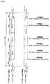
[図1]1シンボル内にライズエッジが複数存在する場合および1シンボル内にライズエッジが1つだけ複数存在するシリアルデータの図である。
[図2]データ長の異なるデジタルデータを示した図である。
[図3]本発明の一実施形態のデジタルデータ送信回路および受信回路並びにデジタルデータ伝送方法およびデジタルデータ伝送システムの概念を示す図である。
[図4]本発明の一実施形態のシリアルデータの概要を示す図である。
[図5]本発明の一実施態様における送信ユニットの回路構成を示す図である。
[図6]本発明の一実施形態における第1のエンコーダ回路2504aの回路ブロック図である。
[図7]本発明の一実施形態における組み合わせ論理回路2504a−1の回路構成を示す図である。
[図8]本発明の一実施態様における第1のエンコーダ回路の回路図及び動作テーブルである。
[図9]本発明の一実施例のエンコード方法のフローチャートである。
[図10]本発明の一実施態様における受信ユニットの回路構成を示す図である。
[図11]本発明の一実施形態における第1のデコーダ回路2524aの回路図である。
[図12]本発明の一実施形態における第2のデコーダ回路2524bの回路図である。
[図13]本発明の一実施形態における第1/第2のデコーダ判別回路2524cの回路図である。
[図14]本発明の一実施形態におけるデコード方法のフローチャートである。
[図15]本発明の一実施形態におけるDEフィルタの回路図及び動作説明図である。
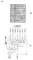
[図16]本発明の受信回路であるクロック抽出回路の回路構成を示すハードウエアブロック図である。
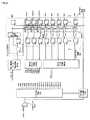
[図17]画像表示の1ライン分のシリアルデータ構成図である。
[図18]ブランキング期間中のシリアルデータの立ち上がりの数と、電圧制御発振器の周Tvcoとの関係図である。
[図19]アクティブ期間中のシリアルデータの立ち上がり数と、電圧制御発振器の周期との関係図である。
[図20]クロックの抽出のプロセスを示すフローチャートである。
[図21]電圧制御発振回路の回路構成を示すハードウエアブロックと各クロック間のタイミングを示す図である。
[図22]サンプラの入出力信号のシリアルデータとサブクロックとのタイミングチャート、およびサンプリング結果のタイミングチャートである。
[図23]エッジ数判定回路の回路構成を示すハードウエアブロック図である。
[図24]エッジ検出回路の回路構成を示すハードウエアブロック図と入出力信号のタイミングチャートである。
[図25]周波数差検出回路の回路構成を示すハードウエアブロック図である。
[図26]タイマの回路構成を示すハードウエアブロック図と各信号のタイミングチャートである。
[図27]チャージポンプの構成を示す回路ブロック図である。
[図28]制御回路の回路構成を示すハードウエアブロック図、そのタイミングチャートおよび制御動作状態遷移図である。
[図29]クロック抽出のプロセスでの電圧制御発振器の周波数の時間変化である。
[図30]デジタルデータをシリアル伝送した際に生じるデータエラーを説明した図である。
[図31]データエラーが生じないデジタルデータのシリアル伝送を説明した図である。
[図32]本発明の一実施例のエンコード方法のフローチャートである。
[図33]本発明の一実施例におけるエンコーダ回路の回路構成図である。
[図34]本発明の一実施例における評価関数の回路構成図である。
[図35]本発明の一実施例のエンコード方法のフローチャートである。
[図36]本発明の一実施例のクロック復元位相同期回路2600の回路構成を示すハードウエアブロック図である。
[図37]本発明の一実施例における微調周波数比較回路80の回路ブロック図である。
[図38]本発明の一実施例のエッジ抽出回路80aの回路構成を示す図である。
[図39]本発明の一実施例のStart/Stop推定回路80bの回路構成を示す図である。
[図40]本発明の一実施例の周波数検出回路80cの回路構成を示す図である。
[図41]本発明の一実施例の送信ユニット3000の概略構成図である。
[図42]本発明の一実施例のCRD検出回路3000の回路構成を示す図である。
[図43]本発明の一実施例の第1のエンコーダ回路の回路構成を示す図である。
[図44]本発明の一実施例のシリアルデジタルデータを示す図である。
[図45]本発明の一実施例を示す図である。
[図46]本発明の一実施例を示す図である。
[図47]本発明の一実施例における送信ユニットを示す図である。
[図48]本発明の一実施例におけるエンコーダ回路を示す図である。
[図49]本発明の一実施例における受信ユニットを示す図である。
[図50]本発明の一実施例におけるデコーダ回路を示す図である。
[図51]本本発明の一実施例における送信ユニットを示す図である。
[図52]本発明の一実施例を示す図である。
[図53]本発明の一実施例のシリアルデジタルデータを示す図である。
[図54]本発明の一実施例における受信ユニットを示す図である。
[図55]本発明の一実施例におけるDEフィルタを示す図である。
[図56]本発明の一実施例のシリアルデジタルデータを示す図である。
[図57]本発明の一実施例を示す図である。
[図58]本発明の一実施例におけるDCバランスエンコーダ回路を示す図である。
[図59]本発明の一実施例を示す図である。
[図60]本発明の一実施例を示す図である。
[図61]本発明の一実施例における送信ユニットを示す図である。
[図62]本発明の一実施例における受信ユニットを示す図である。
[図63]本発明の一実施例のシリアルデジタルデータを示す図である。
[図64]本発明の一実施例におけるクロック抽出回路を示す図である。
[図65]シリアルデータ伝送システムのシステム構成例を示す図である。
[図66]アクティブマトリクス型の液晶ディスプレイに用いられる画像データの構成を示す図である。
[図67]従来のデジタルデータのシリアル伝送を示す図である。
[図68]本発明の一実施例のシリアルデジタルデータを示す図である。
[図69]本発明の一実施例のシリアルデジタルデータを示す図である。
[図70]本発明の一実施例におけるシリアルデータとサンプリングクロックとの関係を示すタイミングチャートである。FIG. 1 is a diagram of serial data when there are a plurality of rise edges in one symbol and when there is only one rise edge in one symbol.
FIG. 2 is a diagram showing digital data having different data lengths.
FIG. 3 is a diagram showing a concept of a digital data transmission circuit and reception circuit, a digital data transmission method, and a digital data transmission system according to an embodiment of the present invention.
FIG. 4 is a diagram showing an outline of serial data according to an embodiment of the present invention.
FIG. 5 is a diagram showing a circuit configuration of a transmission unit in one embodiment of the present invention.
FIG. 6 is a circuit block diagram of a
FIG. 7 is a diagram showing a circuit configuration of a
FIG. 8 is a circuit diagram and an operation table of the first encoder circuit in one embodiment of the present invention.
FIG. 9 is a flowchart of an encoding method according to an embodiment of the present invention.
FIG. 10 is a diagram showing a circuit configuration of a receiving unit in one embodiment of the present invention.
FIG. 11 is a circuit diagram of a
FIG. 12 is a circuit diagram of a
FIG. 13 is a circuit diagram of a first / second
FIG. 14 is a flowchart of a decoding method according to an embodiment of the present invention.
FIG. 15 is a circuit diagram and an operation explanatory diagram of a DE filter in one embodiment of the present invention.
FIG. 16 is a hardware block diagram showing a circuit configuration of a clock extraction circuit which is a receiving circuit of the present invention.
FIG. 17 is a serial data configuration diagram for one line of image display.
FIG. 18 is a relationship diagram between the number of rising serial data during the blanking period and the frequency Tvco of the voltage controlled oscillator.
FIG. 19 is a diagram showing the relationship between the number of rising serial data during the active period and the period of the voltage controlled oscillator.
FIG. 20 is a flowchart showing a clock extraction process.
FIG. 21 is a diagram showing a timing between a hardware block showing a circuit configuration of a voltage controlled oscillation circuit and each clock.
FIG. 22 is a timing chart of serial data of input / output signals of a sampler and a sub clock, and a timing chart of sampling results.
FIG. 23 is a hardware block diagram showing a circuit configuration of an edge number determination circuit.
FIG. 24 is a hardware block diagram showing a circuit configuration of an edge detection circuit and a timing chart of input / output signals.
FIG. 25 is a hardware block diagram showing a circuit configuration of a frequency difference detection circuit.
FIG. 26 is a hardware block diagram showing a circuit configuration of a timer and a timing chart of each signal.
FIG. 27 is a circuit block diagram showing a configuration of a charge pump.
FIG. 28 is a hardware block diagram showing a circuit configuration of a control circuit, a timing chart thereof, and a control operation state transition diagram.
FIG. 29 is a time variation of the frequency of the voltage controlled oscillator in the clock extraction process.
FIG. 30 is a diagram for explaining a data error that occurs when digital data is serially transmitted.
FIG. 31 is a diagram illustrating serial transmission of digital data in which no data error occurs.
FIG. 32 is a flowchart of an encoding method according to an embodiment of the present invention.
FIG. 33 is a circuit configuration diagram of an encoder circuit in an embodiment of the present invention.
FIG. 34 is a circuit configuration diagram of an evaluation function in one embodiment of the present invention.
FIG. 35 is a flowchart of an encoding method according to an embodiment of the present invention.
FIG. 36 is a hardware block diagram showing a circuit configuration of a clock recovery phase synchronization circuit 2600 according to an embodiment of the present invention.
FIG. 37 is a circuit block diagram of a fine tuning
FIG. 38 is a diagram showing a circuit configuration of an edge extraction circuit 80a according to an embodiment of the present invention.
FIG. 39 is a diagram showing a circuit configuration of a start /
FIG. 40 is a diagram showing a circuit configuration of a frequency detection circuit 80c according to an embodiment of the present invention.
FIG. 41 is a schematic configuration diagram of a transmission unit 3000 according to an embodiment of the present invention.
FIG. 42 is a diagram showing a circuit configuration of a CRD detection circuit 3000 according to an embodiment of the present invention.
FIG. 43 is a diagram showing a circuit configuration of a first encoder circuit according to an embodiment of the present invention.
FIG. 44 is a diagram showing serial digital data according to one embodiment of the present invention.
FIG. 45 is a diagram showing an example of the present invention.
FIG. 46 is a diagram showing an example of the present invention.
FIG. 47 is a diagram showing a transmission unit in an embodiment of the present invention.
FIG. 48 is a diagram showing an encoder circuit in one embodiment of the present invention.
FIG. 49 is a diagram showing a receiving unit in an embodiment of the present invention.
FIG. 50 is a diagram showing a decoder circuit in one embodiment of the present invention.
FIG. 51 is a diagram showing a transmission unit in an embodiment of the present invention.
FIG. 52 is a diagram showing an example of the present invention.
FIG. 53 is a diagram showing serial digital data according to one embodiment of the present invention.
FIG. 54 is a diagram showing a receiving unit in an embodiment of the present invention.
FIG. 55 is a diagram showing a DE filter in one embodiment of the present invention.
FIG. 56 is a diagram showing serial digital data according to one embodiment of the present invention.
FIG. 57 is a diagram showing an example of the present invention.
FIG. 58 is a diagram showing a DC balance encoder circuit in one embodiment of the present invention.
FIG. 59 is a diagram showing an example of the present invention.
FIG. 60 is a diagram showing an example of the present invention.
FIG. 61 is a diagram showing a transmission unit in an embodiment of the present invention.
FIG. 62 is a diagram showing a receiving unit in an embodiment of the present invention.
FIG. 63 is a diagram showing serial digital data according to one embodiment of the present invention.
FIG. 64 is a diagram showing a clock extraction circuit in one embodiment of the present invention.
FIG. 65 is a diagram showing a system configuration example of a serial data transmission system.
FIG. 66 is a diagram showing a structure of image data used for an active matrix type liquid crystal display.
FIG. 67 is a diagram showing conventional serial transmission of digital data.
FIG. 68 is a diagram showing serial digital data according to one embodiment of the present invention.
FIG. 69 is a diagram showing serial digital data according to one embodiment of the present invention.
FIG. 70 is a timing chart showing the relationship between serial data and a sampling clock in one embodiment of the present invention.
401 送信ユニット
402 シリアル化回路
403 位相同期回路
404 エンコーダ回路
405 スイッチ回路
406 出力バッファ
411 入力色データ
412 入力同期データ
414 入力クロック
415 シリアルデータ
421 受信ユニット
422 パラレル化回路
423 クロック抽出回路
424 デコーダ回路
425 スイッチ回路
426 スイッチ回路
427 入力バッファ
431 出力色データ
432 出力同期データ
434 出力クロック
2501 送信ユニット
2502 シリアル化回路
2503 位相同期回路
2504 エンコーダ回路
2505 スイッチ回路
2506 出力バッファ
2511 入力色データ
2512 入力同期データ
2514 入力クロック
2515 シリアルデータ
2521 受信ユニット
2522 パラレル化回路
2523 クロック抽出回路
2524 デコーダ回路
2525 スイッチ回路
2526 スイッチ回路
2527 入力バッファ
2531 出力色データ
2532 出力同期データ
2534 出力クロック
10 位相比較回路
20 ループフィルタ
30 電圧制御発振器
40 サンプラ
50 周波数比較回路
51 エッジ数判定回路
52 周波数差検出回路
53 タイマ
60 チャージポンプ
70 制御回路
200 受信回路(クロック復元位相同期回路)
300 シリアルデータ
PLLCLK PLLクロック
SUBCLK サブクロック
DetCLK エッジ検出クロック
NEDG0 ライズエッジ数0
NEDG1 ライズエッジ数1
FQDEN 周波数比較イネーブル信号
PHDEN 位相比較イネーブル信号
FQDRQ 周波数比較要求信号
TIM 1ラインスキャン以上の時間を示す信号
CLK システムクロックタイマ401 transmission unit 402
300 Serial data PLLCLK PLL clock SUBCLK Sub clock DetCLK Edge detection clock NEDG0 Number of rising
NEDG1 Number of
FQDEN Frequency comparison enable signal PHDEN Phase comparison enable signal FQRQ Frequency comparison request signal TIM Signal indicating time longer than one line scan CLK System clock timer
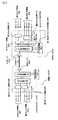
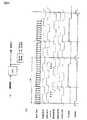
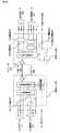
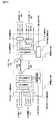
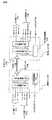
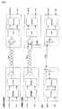
以下、本発明を実施するための最良の形態(以下、実施形態という)について、図面に基づいて説明する。図3に、本実施の形態に係るデータ送信回路および受信回路、並びにそれらを用いたデータ伝送方法およびそのシステムを示す。この送信回路は、送信用LSIとしてパッケージされ、またこの受信回路は、受信用LSIとしてパッケージされ得る。Hereinafter, the best mode for carrying out the present invention (hereinafter referred to as an embodiment) will be described with reference to the drawings. FIG. 3 shows a data transmission circuit and reception circuit according to the present embodiment, and a data transmission method and system using them. The transmission circuit can be packaged as a transmission LSI, and the reception circuit can be packaged as a reception LSI.
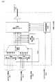
送信ユニット(送信回路)2501は、第1の入力情報2511(本実施の形態においては、入力色データ(RI5〜RI0、GI5〜GI0、BI5〜BI0))、および第2の入力情報2512(入力同期データ(HsyncI(入力水平同期データ)、VsyncI(入力垂直同期データ)、CTRLI(入力コントロール))、第1の入力情報と第2の入力情報の切替信号DEI(入力選択信号(入力データネーブル))をシリアル化したシリアルデータ2515を受信ユニット2521に送信する。このシリアルデータ2515には、入力クロック2514の情報が埋め込まれている。The transmission unit (transmission circuit) 2501 includes first input information 2511 (in this embodiment, input color data (RI5 to RI0, GI5 to GI0, BI5 to BI0)) and second input information 2512 (input). Synchronization data (HsyncI (input horizontal synchronization data), VsyncI (input vertical synchronization data), CTRLI (input control)), switching signal DEI (input selection signal (input data enable)) between the first input information and the second input information ) Is serialized 2515 is transmitted to the receiving unit 2521. In this
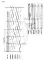
受信ユニット(受信回路)2521は、送信ユニット2501から送信されたシリアルデータ2515を受信し、パラレル化して、第1の出力情報2531(出力色データ(RO5〜RO0、GO5〜GO0、BO5〜BO0))、第2の出力情報2532(HsyncO(出力水平同期データ)、VsyncO(出力垂直同期データ)、CTRLO(出力コントロール)、DEO(出力選択信号(出力データネーブル)))および出力クロック2534に復元して出力する。The reception unit (reception circuit) 2521 receives the
送信ユニット2501は、シリアル化回路2502(Serializer)、位相同期回路2503(PLL回路:Phase Locked Loop回路)、第1のエンコーダ回路2504a(Encoder1)及び第2のエンコーダ回路2504b(Encoder2)、スイッチ回路2505並びに出力バッファ2506(Output Buffer)を有している。The transmission unit 2501 includes a serialization circuit 2502 (Serializer), a phase synchronization circuit 2503 (PLL circuit: Phase Locked Loop circuit), a
また、受信ユニット2521は、パラレル化回路2522(De−serializer)、クロック抽出回路(CDRPLL回路:Clock Data Recovery Phase Locked Loop回路)2523、第1のデコーダ回路2524a(Decoder1)及び第2のデコーダ回路2524b(Decoder2)、第1のスイッチ回路2525及び第2のスイッチ回路2526並びに入力バッファ2527(Input Buffer)を有している。なお、出力バッファ2506および入力バッファ2527は必要に応じて設ければよい。また、本実施形態においては、第1の入力情報2511である入力色データについては、RGB各色のデータが、それぞれ6ビットである例を示しているが、本発明は、8ビットのRGBデータや10ビットのRGBデータ等にも適用でき、本発明は特定のRGBデータビット数に限定されない。また、受信ユニット2521において、第1のデコーダ回路2524a、第2のデコーダ回路2524b、第1のスイッチ回路2525及び第2のスイッチ回路2526は、これらの回路が協調して第1の出力情報2531及び第2の出力情報2532を分離、生成する機能を果たすので、これらの回路を併せて情報分離回路と言うこともある。なお、第1の入力情報2511は第2の出力情報2531に対応しており、第2の入力情報2512は第2の出力情報2532に対応している。The receiving unit 2521 includes a parallelization circuit 2522 (De-serializer), a clock extraction circuit (CDRPLL circuit: Clock Data Recovery Phase Locked Loop circuit) 2523, a
送信ユニット2501においては、第1の入力情報2511及び第2の入力情報2512である入力同期データが、それぞれ、第1のエンコーダ回路2504a及び第2のエンコーダ回路2504bに入力され、エンコードされる。スイッチ回路2505は、DEIを入力選択信号として使用し、DEIがHighの場合は第1のエンコーダ回路2504aによってエンコードされた第1の情報2511を選択し、DEIがLowの場合は第2のエンコーダ回路2504bによってエンコードされた第2の情報2512を選択してシリアル化回路2502へ出力する。入力クロック2514は位相同期回路2503で多相クロックに変換され、シリアル化回路2502はこの多相クロックを用いてスイッチ回路2505の出力をシリアル化しシリアルデータ2515を生成し、出力バッファ2506を通して出力する。In the transmission unit 2501, the input synchronization data as the
送信ユニット2501の第2のエンコーダ回路2504bは、第2の情報(HSYNCI、VSYNCIおよびCTRLI)をエンコードする。その際、第2のエンコーダ回路2504bは、データを順にシリアル化(単純シリアル化)した際に1シンボル内で時間的に先に来る信号をMSBとすると、MSBの値がLSBの値以上となるようにエンコードし、スイッチ回路2505へ出力する。第2の情報期間(本実施形態においては、ブランキング期間(DEI=“Low”)のとき、第2のエンコーダ回路2504bの出力データがスイッチ回路2505によって選択され、シリアル化回路2502によりMSBからLSBに順次シリアル化されて出力される。従って、DEIがLowの場合、シリアル化回路2502によりシリアル化されたデータは、1シンボルにおいて時間的に早い方が高いレベルになっているため、シンボルの切り替わり時のみライズエッジが生じることになる。The
また、送信ユニット2501の第1のエンコーダ回路2504aは、第1の入力情報2511を複数のモード(入力を出力に対応させる対応関係)のうち何れかのモードでエンコードし、スイッチ回路2505へ出力する。第1の情報期間(本実形態においては、アクティブ期間(DEI=“High”))のとき、第1のエンコーダ回路2504aの出力データがスイッチ回路2505によって選択され、シリアル化回路2502によりMSBからLSBに順次シリアル化されて出力される。この第1のエンコーダ2504aにおけるエンコード方法については、後述する。In addition, the
受信ユニット2521においては、まず、クロック抽出回路2523がシリアルデータ2515から出力クロック(CLKO)2534及び多相クロックを復元する。次に、パラレル化回路2522は多相クロックによりシリアルデータ2515をパラレル信号に変換する。このパラレル信号は第1のデコーダ回路2524a、第2のデコーダ回路2524b及び第1/第2のデコーダ判別回路2524cに入力され、デコードされる。第1のスイッチ回路2525は、DEIがHighの時にアクティブとなり、第1のデコーダ回路2524aの出力パラレルデータを第1の出力情報2531(出力色データ(RO5〜RO0、GO5〜GO0、BO5〜BO0))として出力し、DEIがLowの時はLowレベルを出力する。また、第2のスイッチ回路2526は、DEIがLowの時にアクティブとなり、第2のデコーダ回路2524bの出力パラレルデータを第2の出力情報2532(出力同期データ)として出力する。また、DEIがHighの時には出力を保持することが好ましい。これは、DEがHighの期間中に同期データは変化しないためである。In the receiving unit 2521, first, the
次に図4を参照して、本実施形態のデジタルデータ伝送システムのパラレルデータのエンコード方法について説明する。図4(A)および(B)に、パラレルで入力された第1の情報である各6ビットの入力色データ(RI5〜RI0、GI5〜GI0、BI5〜BI0)及び第2の情報である入力同期データ(HsyncI、VsyncI、CTRLIが、送信ユニット2501においてエンコードされ、シリアル化されたシリアルデータ2515の信号波形の例を示す。Next, a parallel data encoding method of the digital data transmission system of this embodiment will be described with reference to FIG. 4 (A) and 4 (B), 6-bit input color data (RI5 to RI0, GI5 to GI0, BI5 to BI0) as first information input in parallel and input as second information are shown in FIG. An example of a signal waveform of
図4(A)に示すように、DEI=“Low”即ちブランキング期間において、シリアルデータ2515の21ビットで構成される1シンボルは、MSBであるスタートビット(Start)とLSBであるストップビット(Stop)の間にHsyncI、VsyncIおよびCTRLIの情報が埋め込まれている。このHsyncI、VsyncIおよびCTRLIの3ビットの情報は、エンコーダ回路2504において、順にシリアル化された後にパルス幅変調(PWM)データとなるようにエンコードされる。すなわち、スタートビットを“High”としたときには、HsyncI、VsyncIおよびCTRLIの3ビットの情報を“High”ビットパルスの時間幅に変調する。図4(A)に示す例では、2ビット幅を単位として0から7(0から14ビット幅)のパルス幅変調を行っている。図4(A)では、この14ビット幅のパルス幅変調信号を、1シンボルのMSBのスタートビットから4ビット目から埋め込んでいる例を示したが、スタートビットのレベルと同じレベルのビットから開始し、1シンボルの終了までに14ビット幅が収まればどのビットから埋め込むものとしてもよい。例えば、1シンボルのMSBのスタートビットから4ビット目からPWMデータを埋め込んだ場合には、1シンボルの終端部にはストップビットを含めてPWMデータでないビットが3ビット存在する。この終端部の3ビットは、ストップビットと同じ“Low”レベルである。このようにシリアル化されたシリアルデータ2515は、図4(A)に示すように1シンボル中のライズエッジが1つしか存在しないデータ構成となる。以上、スタートビットが“High”で、ストップビットが“Low”で、PWM変調データが“High”のパルス幅である例を説明したが、1シンボル中のライズエッジが1つしか存在しないデータ構成とできれば、スタートビット、ストップビット、およびPWM変調ビットのレベルはこの例に限らない。すなわち、例えばスタートビットが“Low”、ストップビットが“High”、およびPWM変調ビットが“Low”としたシリアルデータであっても、1シンボル中のライズエッジが1つしか存在しないデータを構成することができ、このようなシリアルデータも本発明のシステムに用いることができる。また、図4(A)に示す例では、PWMデータを2ビット単位で構成するものとしたが、PWMデータは2ビット以外の単位、例えば1ビット幅単位で構成しても良い。なお、DEI=“Low”の場合は、第1の入力情報を構成するデジタルデータのパルス幅の21倍の周期で、第2の入力情報がパルス幅変調されることになる。As shown in FIG. 4A, in the DEI = “Low”, that is, in the blanking period, one symbol composed of 21 bits of the
HsyncI、VsyncIおよびCTRLIの情報が埋め込まれたPWM信号以外の2パターンには、他の情報を埋め込むこともできる。たとえばこの2パターンに音声情報を埋め込むことも可能である。Other information can be embedded in two patterns other than the PWM signal in which the information of HsyncI, VsyncI, and CTRLI is embedded. For example, audio information can be embedded in these two patterns.
次に、DEI=“High”即ちアクティブ期間においては、図4(B)に示すようにシリアルデータ2515の1シンボルは、スタートビット(Start)、エンコードされた第1の入力情報(RI5〜RI0、GI5〜GI0、BI5〜BI0)からなるシリアルデジタルデータD<17:0>、及び1ビットのエンコードビットEn(エンコードモード識別情報とも言う。)、およびストップビット(Stop)の順でシリアライズされたデータによって構成されている。DEI=“High”の場合に、1シンボル中のライズエッジが2つ以上存在するシリアルデータとするために、第1のエンコーダ回路2504aは、第1の入力情報を、図4(B)に示すように、アクティブ1モード(ACTV symbol/1)及びアクティブ2モード(ACTV symbol/2)の何れかのモードでエンコードし、シリアル化させる。本実施例においては、1シンボル中のライズエッジの数、即ち遷移の数が2以上になるように、アクティブ1モードとアクティブ2モードの何れかのエンコードモードが選択される。Next, in DEI = “High”, that is, in the active period, as shown in FIG. 4B, one symbol of the
本実施例においては、図4(B)に示すとおり、シリアルデータ2515において、2通りのいずれのエンコードモードによりエンコードされたデータであるかを区別するために、エンコードビットを有する。本実施例では、エンコードビットの一例として、アクティブ1モードでエンコードされた場合は、ストップビット(stop)の前にエンコードビット(En)としてデータ“1”が付加され、またアクティブ2モードでエンコードされた場合は、ストップビット(stop)の前にエンコードビット(En)としてデータ“0”が付加されるようにし、アクティブ1モードでエンコードされたデータとアクティブ2モードでエンコードされたデータとを判別できるようにしている。In the present embodiment, as shown in FIG. 4B, the
また、本発明において、DEI=“Low”の場合は、1シンボル中のライズエッジの数が1であるので、DEI=“High”の場合は、1シンボル中のライズエッジの数が1とならないようにアクティブ1モードとアクティブ2モードとの何れかのエンコードモードが選択され、シリアルデータが作成される。In the present invention, when DEI = “Low”, the number of rise edges in one symbol is 1. Therefore, when DEI = “High”, the number of rise edges in one symbol is not 1. As described above, either the active 1 mode or the active 2 mode is selected, and serial data is created.
図4に示すとおり、本実施形態においては、アクティブ2モードによってエンコードされたシリアルデータは、アクティブ1モードによってエンコードされたシリアルデータに対して、2ビット毎に2ビットずつ反転させる構成を採っている。即ち、アクティブ1モードによってエンコードされたシリアルデータD<17:0>に対して、アクティブ2モードによってエンコードされたシリアルデータは、D<D17,D16,反転D15,反転D14,D13,D12,・・・D5,D4,反転D3,反転D2,D1,D0>といった構成を採る。なお、アクティブ1モードとアクティブ2モードによるエンコードの方法は、これに限定されるわけではなく、1シンボル中のライズエッジ即ち遷移の数が2以上となるようなエンコード方法が適用され得る。As shown in FIG. 4, in this embodiment, the serial data encoded in the active 2 mode is configured to invert 2 bits every 2 bits with respect to the serial data encoded in the active 1 mode. . That is, serial data encoded by the active 2 mode is D <D17, D16, inversion D15, inversion D14, D13, D12,... With respect to the serial data D <17: 0> encoded by the active 1 mode. -D5, D4, inversion D3, inversion D2, D1, D0> are adopted. The encoding method in the active 1 mode and the active 2 mode is not limited to this, and an encoding method in which the number of rise edges, that is, transitions in one symbol is 2 or more can be applied.
(送信ユニット)
ここで、図5を用いて本発明のデジタルデータ伝送システムの送信ユニット2501の構成及び各構成要素の接続構成について説明する。図5に示すとおり、スイッチ回路2505には、第1のエンコーダ回路2504a及び第2のエンコーダ回路2504bからの出力が入力される。スイッチ回路2505は、20個のマルチプレクサを有している。なお、図5に示すとおり、本実施形態においては、第1のエンコーダ回路2404aからの18ビット(ENCD1〜18)の出力と、第2のエンコーダ回路2504bからの7ビットの出力がスイッチ回路2505に入力される。(Transmission unit)
Here, the configuration of the transmission unit 2501 of the digital data transmission system of the present invention and the connection configuration of each component will be described with reference to FIG. As shown in FIG. 5, the output from the
次に図6を参照する。図6は、本実施形態における第1のエンコーダ回路2504aの回路ブロック図を示す。第1のエンコーダ回路2504aは、組み合わせ論理回路2504a−1及び判定回路2504a−2を有している。第1の入力情報2511(D<17:0>)は、組み合わせ論理回路2504a−1及び判定回路2504a−2へ入力される。判定回路2504a−2は、第1の入力情報2511に基づき、アクティブ1モード及びアクティブ2モードのうち何れのモードで第1の入力情報2511をエンコードするかを判定し、この判定に基づいた判定信号を出力する。本実施形態において、判定回路2504a−2が出力する判定信号は、組み合わせ論理回路2504a−1にアクティブ1モードのエンコードをさせる場合には“High”レベルの信号であり、アクティブ2モードのエンコードをさせる場合には“Low”レベルの信号としている。この判定信号は、エンコードビットEnとしても用いられる。組み合わせ論理回路2504a−1は、第1の入力情報2511を、判定信号に応じてアクティブ1モード又はアクティブ2モードでエンコードし、出力する。また、判定回路2504a−2は、第1の入力情報2511のみからではなく、第1の情報の伝送周波数、EMI量、第1の情報の1シンボルのシリアルデジタルデータ及び第2の情報のパルス幅変調信号のSN比又はエラーレートのうち少なくとも一つに基づいて評価するようにしてもよい。この場合、判定回路2504a−2は、第1の入力情報以外に、これらの情報を取得する。このような構成をとることにより、第1のエンコーダ回路2505aは、第1の情報の伝送周波数、EMI量、第1の情報の1シンボルのシリアルデジタルデータ及び第2の情報のパルス幅変調信号のSN比又はエラーレートが良くなるモードでエンコードを行うことができ、総合的に伝送特性を向上させることができる。Reference is now made to FIG. FIG. 6 shows a circuit block diagram of the
なお、本実施の形態においては、第1のエンコーダ回路2504aは、アクティブ1モード及びアクティブ2モードの2つのモードのうち何れかのモードによってデータをエンコードするようにしているが、本発明においては、これに限定されるわけではなく、組み合わせ論理回路2504aは、2以上のエンコードモード(例えば、n個のモード)を有し、そのうち何れかのモードでデータをエンコードするようにしてもよい。この場合、判定回路2504a−2は、(log2n)ビットの判定信号を生成し、組み合わせ論理回路2504a−1に出力することになる。ここで、エンコードモードの相違は、入力と出力との対応関係が相違していることを意味する。したがって、エンコードモードが異なれば、入力と出力との対応関係が異なっている。In the present embodiment, the
次に図7を参照し、第1のエンコーダ回路2504aの組み合わせ論理回路2504a−1の回路構成について説明する。組み合わせ論理回路2504a−1は、第1の入力情報2511のビット数に対応した数の排他的論理和回路(XOR回路)及びスイッチ回路を有している。各スイッチ回路には、アクティブ1モードに対応したデータ及びアクティブ2モードに対応したデータが入力される。各スイッチ回路は、判定回路2504a−2からの判定信号によって、アクティブ1モードに対応したデータ又はアクティブ2モードに対応したデータを選択し、各XOR回路へ出力する。各XOR回路には、第1の入力情報2511及び各スイッチ回路からの出力が入力され、各XOR回路によって論理演算される。各XOR回路の出力は第1のスイッチ回路2525へ入力される。Next, a circuit configuration of the
次に、図8(A)および(B)を参照し、第2のエンコーダ回路2504bの動作について説明する。図8(A)に、本実施形態の第2のエンコーダ回路2504bの回路構成及びその7ビットの出力(SYNC[0]〜SYNC[6])を示す。また、図8(B)には、本実施形態の第2のエンコーダ回路2504bに入力されるHsync、VsyncおよびCTRLIとその出力データ(SYNC[0]〜SYNC[6])のデータテーブルが示されている。Next, the operation of the
図8(B)のデータテーブルに示すとおり、第2のエンコーダ回路2504bからの出力データ(SYNC[0]〜SYNC[6])は、入力データHsync、VsyncおよびCTRLIを入力したときに、遷移の数が制限された形となっている。言い換えると、最上位ビット(MSB)をHsyncI、最下位ビット(LSB)をCTRLIとする3ビットのデータ{Hsync、Vsync、CTRLI}を7ビットのデータ{SYNC[0](最上位ビット)〜SYNC[6](最下位ビット)}にエンコードする際に、当該3ビットのデータが1増す毎に、当該7ビットのデータの最上位ビットから順に“High”データが出力され続けるようにエンコードする。さらに言い換えると、7ビットのデータ{SYNC[0](最上位ビット)〜SYNC[6](最下位ビット)}において常に上位ビットの値が下位ビットの値以上であるデータが出力されるようにエンコードする。このような出力形態は一般的には“Thermo−Code(サーモコード)”と言われており、このようなエンコードは“Thermo−Code(サーモコード)”型のエンコード、また、このようなエンコーダは“Thermo−Code”型のエンコーダと言われている。As shown in the data table of FIG. 8B, the output data (SYNC [0] to SYNC [6]) from the
本発明のデータ伝送方法およびそのシステムにおける第2のエンコーダ回路2504bは、サーモコード型の出力形態をとる。なお、第2のエンコーダ回路2504bの回路構成については、図8(A)に示すものに限定されるわけではなく、サーモコード型の出力形態をとる回路構成であれば如何なる回路構成をとってもよい。かくして、1シンボル内にライズエッジが1つのみ生成される。The
ここで、再度図5を参照する。第1のエンコーダ回路2404aからの出力データ(ENCD1〜19)並びに第2のエンコーダ回路2404bからの出力データ(SYNC[0]〜SYNC[6])及びDEI(入力データイネーブル)は、スイッチ回路2505へ入力される。スイッチ回路2505は、入力されるDEIに基づき、DEI=“High”のときは、第1のエンコーダ回路2404aからの出力データ(ENCD1〜19)を選択し、また、DEI=“Low”のときは、第2のエンコーダ回路2404bからの出力データ(SYNC[0]〜SYNC[6])を選択して、シリアル回路2502にデータ(SR0〜SR19)を出力する。Here, FIG. 5 will be referred to again. Output data (ENCD1 to 19) from the first encoder circuit 2404a, output data (SYNC [0] to SYNC [6]) and DEI (input data enable) from the second encoder circuit 2404b are sent to the
位相同期回路2503は、入力クロック2514に基づき位相の異なる複数のクロックを形成し、シリアル化回路2502へ出力する。The
シリアル化回路2502は、入力されるデータ(SR0〜SR19)を位相同期回路2503から入力される位相の異なる複数のクロックに基づきシリアル化し、シリアルデータ2515を形成し、出力バッファ2506を通して受信ユニット2521へ出力する。このシリアルデータ2515の形成において、1シンボルの先頭に“High”のスタートビットと、後尾に“Low”のストップビットを形成するために、シリアル化回路2502には、“High”レベルと“Low”レベルの信号が入力される。The
ここで、本実施形態のデータ伝送システムにおける入力情報に応じたエンコードモードの仕分けについて、図9を参照しながら詳細に説明する。図9に、本実施形態に係るエンコードモードの仕分け方法のフローチャートを示す。Here, the sorting of the encoding mode according to the input information in the data transmission system of the present embodiment will be described in detail with reference to FIG. FIG. 9 shows a flowchart of an encoding mode sorting method according to the present embodiment.
まず、入力情報(パラレルデータ)のDEIが“High”か“Low”か判断する(ステップS1)。ステップS1において、DEI=“Low”の場合は、第2の情報(HsyncI、VsyncIおよびCTRLI)を、順にシリアル化したときにパルス幅変調(PWM)信号となるようにエンコードする。このエンコードによれば、シリアル化した後に、1シンボル中のライズエッジの数が1つしか存在しないデータ構成をとるようにできる(ステップS2)。以上により第2の情報のデータのエンコードが終了する(ステップS3)。First, it is determined whether the DEI of the input information (parallel data) is “High” or “Low” (step S1). In step S1, when DEI = “Low”, the second information (HsyncI, VsyncI and CTRLI) is encoded so as to become a pulse width modulation (PWM) signal when serialized in order. According to this encoding, after serialization, it is possible to adopt a data configuration in which there is only one rise edge in one symbol (step S2). Thus, the encoding of the second information data is completed (step S3).
ステップS1において、DEI=“High”の場合は、入力色データ(RI5〜RI0、GI5〜GI0、BI5〜BI0)をエンコードする際、アクティブ1モードでエンコードし、その前後に互いに符号の異なるスタートビットとストップビットとを付加したシリアル化をすると1シンボル中にライズエッジの数が1つとなるかどうかを判断し(ステップS4)、1シンボル中にライズエッジの数が1つとなる場合は、第1の情報(RI5〜RI0、GI5〜GI0、BI5〜BI0)をアクティブ2モードでエンコードし(ステップS5)、データのエンコードを終了する(ステップS6)。一方、1シンボル中にライズエッジの数が2つ以上となる場合は、ステップ7の処理を行う。ステップ7においては、第1の情報(RI5〜RI0、GI5〜GI0、BI5〜BI0)をエンコードする際、アクティブ2モードでエンコードし、その前後に互いに符号の異なるスタートビットとストップビットとを付加したシリアル化をすると1シンボル中にライズエッジの数が1つとなるかどうかを判断し(ステップS7)、1シンボル中にライズエッジの数が1つとなる場合は、第1の情報(RI5〜RI0、GI5〜GI0、BI5〜BI0)をアクティブ1モードでエンコードし(ステップS8)、データのエンコードを終了し(ステップS9)、1シンボル中にライズエッジの数が2つ以上となる場合は、ステップS10の処理を行う。In step S1, when DEI = “High”, the input color data (RI5 to RI0, GI5 to GI0, BI5 to BI0) are encoded in the active 1 mode, and before and after the start bits having different signs. When the serialization with the stop bit added is performed, it is determined whether or not the number of rise edges is one in one symbol (step S4). (RI5 to RI0, GI5 to GI0, BI5 to BI0) are encoded in the active 2 mode (step S5), and the data encoding is terminated (step S6). On the other hand, if the number of rise edges in one symbol is two or more, the process of
以上、第1の情報である入力色データを単純シリアル変換し、その前後に互いに符号の異なるスタートビットとストップビットとを付加したときに、ライズエッジ数が1であるかについて評価を行い、判定するものとしたが、スタートビットとストップビットとを考慮せず、第1の情報である入力色データを単純シリアル変換した場合のシリアルデータを評価してもよい。この場合、ライズエッジの数が0であるか否か判定することになる。As described above, when the input color data, which is the first information, is subjected to simple serial conversion, and the start bit and stop bit having different signs are added before and after the evaluation, it is evaluated whether or not the number of rise edges is 1. However, the serial data when the input color data as the first information is subjected to simple serial conversion may be evaluated without considering the start bit and the stop bit. In this case, it is determined whether or not the number of rise edges is zero.
ステップS10においては、アクティブ1モード又はアクティブ2モードの何れのモードでエンコードするかを所定の評価関数によって評価し、その評価に基づいてアクティブ1モードでエンコードする(ステップS8)か、アクティブ2モードでエンコードする(ステップS5)か判定する。このエンコードにより第1の情報のデータのエンコードが完了する(ステップS9又はステップS6)。なお、ステップS10においては、アクティブ1モード又はアクティブ2モード何れのモードでエンコードした場合であっても、DEI=“Low”である場合のシリアルデータ(ライズエッジの数が1つ)と同一にはならない。In step S10, whether the active 1 mode or the active 2 mode is encoded is evaluated by a predetermined evaluation function. Based on the evaluation, encoding is performed in the active 1 mode (step S8) or in the active 2 mode. It is determined whether to encode (step S5). This encoding completes the encoding of the first information data (step S9 or step S6). Note that in step S10, even if encoding is performed in either the active 1 mode or the active 2 mode, it is the same as the serial data (the number of rise edges is 1) when DEI = “Low”. Don't be.
以上のようなエンコード処理を行うことによって、DEI=“Low”の場合と、DEI=“High”の場合におけるエンコードされたデータからなるシリアルデータは、1シンボル中のライズエッジの数が1つであるか(DEI=“Low”の場合)又は1シンボル中のライズエッジの数が2つ以上であるか(DEI=“High”の場合)が明確に区別される。By performing the encoding process as described above, serial data composed of encoded data in the case of DEI = “Low” and DEI = “High” has one rise edge in one symbol. It is clearly discriminated whether there is (when DEI = “Low”) or the number of rise edges in one symbol is two or more (when DEI = “High”).
以上のように、パラレルで入力される第1の情報2511及び第2の情報2512がエンコードされた後、シリアル化され、シリアルデータ2515として送信ユニット2501から受信ユニット2521へ伝送される。このようにシリアル化されたシリアルデータの伝送において、第1の情報2511のシリアルデータの1シンボルを伝送する期間を第1の期間といい、第2の情報2512のシリアルデータの1シンボルを伝送する期間を第2の期間という。したがって、第1の期間における第1の情報の単位時間あたりの情報量は、第2の期間における第2の情報の単位時間あたりの情報量よりも多くなっている。As described above, the
以上、図3に示す本実施形態においては、シリアル化回路2502の前段にスイッチ回路2505を配置し、先にスイッチ回路2505が、第1のエンコーダ回路2504aによってエンコードされた第1の情報2511と第2のエンコーダ回路2504bによってエンコードされた第2の情報2512とをDEIに基づいて選択した後、シリアル化回路2502がこれら選択されたデータを順にシリアル化する構成とした。一方、シリアル化回路2502をスイッチ回路2505の前段に配置し、第1のエンコーダ回路2504aによってエンコードされた第1の情報2511と第2のエンコーダ回路2504bによってエンコードされた第2の情報2512とをシリアル化回路2502においてそれぞれシリアル化した後、スイッチ回路2505が第1の情報のシリアルデータと第2のシリアルデータとを交互に周期的にシリアル化する構成とすることもできる。As described above, in the present embodiment shown in FIG. 3, the
(受信ユニット)
図10に、本実施形態の受信ユニット2521の構成を示す。送信ユニット2501から出力されたシリアルデータ2515は、入力バッファ2527を通してパラレル化回路2522およびクロック抽出回路2523へ入力される。クロック抽出回路2523は、シリアルデータ2515からクロックを抽出し、出力クロック2534および位相の異なる複数のクロックを復元する。パラレル化回路2522は、クロック抽出回路2523によって復元された位相の異なる複数のクロックに基づき、シリアルデータ2515をパラレル化し、その出力データ(DSR0〜DSR20)を第1のデコーダ回路2524a、第2のデコーダ回路2524b及び第1/第2のデコーダ判別回路2524cへ出力する。第1のデコーダ回路2524aには、第1の入力情報2511に対応する出力データ(DSR1〜19)が入力され、第2のデコーダ回路2524bには、出力データ(本実施形態においては、DSR4、DSR6、DSR8、DSR10、DSR12、DSR14、DSR16)が入力される。また、第1/第2のデコーダ判別回路2524cには、出力データ(DSR1〜19)が入力される。各デコーダ回路2524a、2524bは、入力されたデータをデコードし、それぞれ、第1の入力情報2511及び第2の入力情報に対応するデータをスイッチ回路2525、2526へ出力する。(Receiving unit)
FIG. 10 shows the configuration of the receiving unit 2521 of this embodiment.
なお、受信ユニット2521は、図10に示すように、DEフィルタ2540及びフリップフロップ回路2541を備えるようにしても良い。この場合、第1/第2のデコーダ判別回路2524cの出力データは、DEフィルタ2540で処理され、その出力が第1のスイッチ回路2525及び第2のスイッチ回路2526へ入力される。なお、DEフィルタ2540の動作は後に詳細に説明する。Note that the receiving unit 2521 may include a DE filter 2540 and a flip-
ここで、本実施形態の第1のデコーダ回路2524aについて図11を参照して説明する。図11に、本実施形態に係る第1のデコーダ回路2524aの回路構成図を示す。エンコードビット(En)に対応するDSR<19>が、“Low”=0の場合、アクティブ2モードによるエンコード方法に対応させた所定のデータ(マスク″001100・・・・″)とDSR<1:18>の排他的論理和(XOR)をとり、D<17:0>を第1のスイッチ回路2525へ出力する。また、DSR<19>が“High”=1の場合、アクティブ1モードのエンコードに対応してDSR<1:18>をそのままD<17:0>として第1のスイッチ回路2525へ出力する。Here, the
次に、本実施形態の第2のデコーダ回路2524bの回路構成について図12を用いて説明する。第2のデコーダ回路2524bは、12個のNOR回路、1つのNAND回路および2つのインバータ回路を有している。なお、第2のデコーダ回路2524bは、“Thermo−code”化された同期信号をデコードする回路構成であればよく、図12に示す回路構成に限定されるわけではない。Next, the circuit configuration of the
次に、図13を参照し、第1/第2のデコーダ判別回路2524cの回路構成について説明する。第1/第2のデコーダ判別回路2524cは、パラレル化回路2522からの出力データ(DSR1〜19)が入力される18個のAND回路(1st stage)とそれらの出力が入力されるOR回路(2nd stage)を有している。1st stageでは、DSR<1>からDSR<19>までの各ビット間にライズエッジがあるかどうかを判定する。2nd stageでは、1st stageの出力に1つでもHighがあればDEI=“High”と判断してHigh”(=“1”)のDEOを出力し、1st stageの出力にHighが1つもなければDEI=“Low”と判定し“Low”(=“0”)のDEOを出力する。同期がとれている状態では、DSR<20>とDSR<0>は、それぞれ、ストップビット(Stop)、スタートビット(Start)であるから、この間にライズエッジが1個あることは確定しているため、結局、第1/第2のデコーダ判別回路2524cにおいては、1シンボル中にライズエッジが1個あるか、それ以上あるかを判定していることになる。Next, the circuit configuration of the first / second
ここで、図14を参照し、本実施形態の受信ユニット2521におけるデコード方法をフローチャートを用いて説明する。まず、パラレル化回路2522によってパラレル化された1シンボルのデータ中にライズエッジの数が1であるかどうかを判断する(ステップS1)。ライズエッジの数が1である場合は、この1シンボルのデータは、第2の情報(同期信号(HsyncI、VsyncI、CTRLI))であるので、第2のデコーダ回路2524bは、これら第2の情報をデコードし(ステップS2)、データのデコードが終了する(ステップS3)。一方、ライズエッジの数が2以上である場合は、この1シンボルのデータは第1の情報(色データ信号(RI5〜RI0、GI5〜GI0、BI5〜BI0))であり、さらにエンコードビット(En)のデータが“1”であるか“0”であるかを判断する(ステップS4)。第1のデコーダ回路2524aは、エンコードビット(En)のデータが“1”である場合に、パラレル化された1シンボルのデータをアクティブ1モードのエンコードに対応したアクティブ1モードでデコードし(ステップS5)、エンコードビット(En)のデータが“0”である場合は、パラレル化された1シンボルのデータをアクティブ2モードのエンコードに対応したアクティブ2モードでデコードし(ステップS7)、デコードが終了する(ステップS6、S8)。Here, with reference to FIG. 14, the decoding method in the receiving unit 2521 of this embodiment is demonstrated using a flowchart. First, it is determined whether or not the number of rise edges is 1 in the data of one symbol parallelized by the parallelizing circuit 2522 (step S1). When the number of rise edges is 1, the data of one symbol is the second information (synchronization signals (HsyncI, VsyncI, CTRLI)), and therefore the
再度図10を参照する。第1のスイッチ回路2525は、第1のデコーダ回路2524aから入力されるデータを、クロック抽出回路2523から入力される位相の異なる複数のクロックに基づき選択し、フリップフロップ回路2542へ出力する。また、第2のスイッチ回路2526は、第2のデコーダ回路2524bから入力されるデータを、クロック抽出回路2523から入力される位相の異なる複数のクロックに基づき選択し、フリップフロップ回路2542へ出力する。フリップフロップ回路2542は、19個のフリップフロップから成り、第1の出力情報(RO5〜RO0、GO5〜GO0、BO5〜BO0)及び第2の出力情報(HsyncO、YsyncO、CTRLO)を出力する。Refer to FIG. 10 again. The first switch circuit 2525 selects the data input from the
このようにして、送信ユニット2501にパラレルに入力される第1の情報2511、第2の情報2512、DEIおよび入力クロック2514は、シリアル化された後送信される。受信ユニット2521で受信されたシリアルデータは、パラレル化された後、デコードされ、第1の出力情報2531、第2の出力情報2532、DEOおよび出力クロック2534に復元されて出力される。In this way, the
次に、図15を用いてDEフィルタ2540の動作について説明する。図15(A)に、DEフィルタ2540の回路構成を示し、図15(B)に、DEフィルタ2540におけるデータ(DE0、DE1、DE2、DEO)のタイミングチャートを示す。本実施形態に係るDEフィルタ2540は、1つのOR回路及び3つのAND回路からなる多数決回路2540a及び3つのフリップフロップを有している。Next, the operation of the DE filter 2540 will be described with reference to FIG. FIG. 15A shows a circuit configuration of the DE filter 2540, and FIG. 15B shows a timing chart of data (DE0, DE1, DE2, DEO) in the DE filter 2540. The DE filter 2540 according to the present embodiment has a majority circuit 2540a composed of one OR circuit and three AND circuits, and three flip-flops.
DEI信号は、1ビット分だけのパルス幅の信号ではなく、数ビット続く信号である。従って、DEI信号に1ビット分だけのパルスがあればそれは真のデータでは無く、エラーである。DEフィルタ2540はこのエラーを除去する。DEフィルタ2540はDEIを遅延させるためのフリップフロップ回路と多数決回路2540aで構成される。多数決回路2540aは3つの入力のうちで1が多ければ1を、0が多ければ0を出力する。図15(B)に示した波形例では、太線で示したエラーを多数決回路2540でフィルタしている。図15(A)に示す回路構成をとることにより、DEフィルタ2540に入力されるDEOにシリアルデータの1ビットのパルス幅のエラーを含んでいても、当該エラーを除去したDEOを出力することができる。以上、フリップフロップを直列に2段接続し、1ビット周期ずつタイミングをシフトさせた3つの信号(DE0,DE1,DE2)の多数決を採るものとしたが、信号の多数決は3つに限られない。例えば、フリップフロップを直列に4段接続し、1ビット周期ずつタイミングをシフトさせた5つの信号の多数決を採るものとしてもよい。The DEI signal is not a signal having a pulse width of one bit but a signal that lasts several bits. Therefore, if there is a pulse of only one bit in the DEI signal, it is not true data but an error. The DE filter 2540 eliminates this error. The DE filter 2540 includes a flip-flop circuit for delaying the DEI and a majority circuit 2540a. The majority voting
(クロック抽出回路)
以下画像データの伝送を例に、図を用いて本発明の受信回路の実施例を詳細に説明する。図16は、本発明の受信回路であるクロック復元位相同期回路(クロック抽出回路)の回路構成を示すハードウエアブロック図である。このクロック抽出回路は、図3におけるクロック抽出回路2523に相当する。図17は、送信側の送信ユニットで、パラレルの画像データがシリアルデータ化されて送信される、シリアルデータ構成を示す図である。最初に、図16に示されるクロック復元位相同期回路への入力信号であるシリアルデータのデータ構成を説明する。図17は、画像表示における1ラインをスキャンするに必要なシリアルデータ構成を示し、任意の1ライン期間(tLine)は、ブランキング期間(tSync)およびアクティブ期間(tActive)から成っている。いずれにおいても、スタート/ストップの1/0で区切られた21ビットが、1シンボルとして伝送される。位相同期に必要な位相比較は、このスタート/ストップを手がかりに行われる。(Clock extraction circuit)
In the following, an embodiment of the receiving circuit of the present invention will be described in detail with reference to the drawings, taking image data transmission as an example. FIG. 16 is a hardware block diagram showing a circuit configuration of a clock recovery phase synchronization circuit (clock extraction circuit) which is a receiving circuit of the present invention. This clock extraction circuit corresponds to the
入力データのブランキング期間(tSync)において、シリアルデータ300の1シンボルは、スタートビット(Start)、エンコードされた水平同期データ(HsyncI)、垂直同期データ(VsyncI)およびコントロールデータ(CTRLI)、およびストップビット(Stop)の順でシリアライズされたデータによって構成されている。具体的には、ブランキング期間中のシリアルデータは、ライズエッジの周期が一定で、フォールエッジがHsync、VsyncおよびCTRLIによって変化するパルス幅変調された形になっている。In the blanking period (tSync) of the input data, one symbol of the
一方、アクティブ期間(tActive)においては、シリアルデータ300の1シンボルは、スタートビット(Start)、カラーデータビット(R、G、B各6ビット)の18ビットをエンコードした19ビット、およびストップビット(Stop)の順で、21ビットがシリアライズされたデータとして構成されている。なおR、G、Bデータのエンコードは、シンボル内のライズエッジが2以上になるように行われた後、シリアライズされている。本実施例においてシリアルデータを構成するカラーデータは、それぞれ6ビットのRGBデータであるとしたが、これに限定されるわけではない。On the other hand, in the active period (tActive), one symbol of the
送信ユニット側から送られてきたこのシリアルデータを、受信ユニット側でパラレルデータに変換する際のクロックの復元について、次に説明する。図18は、ブランキング期間におけるシリアルデータ300の1シンボル周期(To)内のシリアルデータの立ち上がり(ライズエッジ)の数と、後述する電圧制御発振器の周期(Tvco)との関係を示す図である。シリアルデータ300における1シンボル中のライズエッジは、1つしか存在しないようにデータ構成が取られているため、Toに比べてTvcoが短い場合、即ち電圧制御発振器の周波数(fvco)がToの周波数(fo)より高い場合は、Tvco内のライズエッジの数(NEDG)は1または0となる。fvco=foの場合は、NEDG=1となり、fvco<foの場合は、NEDG=1または2となる。従って、fvcoとfoとの大小関係をNEDGを評価することで場合分けすることができる。Next, the restoration of the clock when the serial data sent from the transmission unit side is converted into parallel data on the reception unit side will be described. FIG. 18 is a diagram showing the relationship between the number of rises (rise edges) of serial data within one symbol period (To) of the
図19は、アクティブ期間におけるシリアルデータ300の1シンボル周期(To)内のシリアルデータの立ち上がり(ライズエッジ)の数と、後述する電圧制御発振器の周期(Tvco)との関係を示す図である。シリアルデータ300における1シンボル中のライズエッジは、To>Tvcoの場合、即ち電圧制御発振器の周波数(fvco)がToの周波数(fo)より高い場合は、ライズエッジの数(NEDG)は1以上または0以上となる。fvco=foの場合は、NEDG=1以上となり、fvco<foの場合は、NEDG=1以上または2以上となる。従って、アクティブ期間においては、NEDGだけからfvcoとfoとの大小関係を判断できない。FIG. 19 is a diagram showing the relationship between the number of rises (rise edges) of serial data within one symbol period (To) of the
以上の説明を基にして、周波数差を以下のように判別できる。
(1)NEDG=0であれば、fvco>fo
(2)NEDG=1がある程度連続すれば、fvco≒fo(連続する数をNとすれば、fvcoとfoの差≒fo/Nとなる。実施例においては、N=30〜50とする)
(3)ブランキング期間を経過したにもかかわらず、(1)、(2)が起きなければ、fvco<fo(これは、後述するtTME期間中に必ずブランキングを経るように、tLineよりも十分長いtTMEを設定することによる)Based on the above description, the frequency difference can be determined as follows.
(1) If NEDG = 0, fvco> fo
(2) If NEDG = 1 continues to some extent, fvco≈fo (if the number of consecutive is N, the difference between fvco and fo≈fo / N. In the embodiment, N = 30 to 50)
(3) If (1) and (2) do not occur even though the blanking period has elapsed, fvco <fo (this is more than tLine so that blanking is always performed during the tTME period described later). (By setting a sufficiently long tTME)
図20は、図18、図19で説明したfvcoのfoとの大小関係と、NEDGとの関係を基にクロックの復元を行うプロセスを示すフローチャートである。受信したシリアルデータを、後述する電圧制御発振回路で生成されたサンプリングパルスでサンプリングする(ステップ100)。次にサンプリング結果に基づきTvco内のシリアルデータのライズエッジの数をカウントし、NEDG=0か否かを判断する(ステップ110)。NEDG=0でなければ、NEDG=1の連続数(NNEDG1)が所定の数値(NNEDG1th)以上か否かを判断する(ステップ120)。NNEDG1が所定の数値以上の場合は位相比較ループのキャプチャレンジに入ったと判断し、位相比較を開始する(ステップ130)。ステップ110においてNEDG=0であれば、fvcoが高いと判断し、電圧制御発振回路の周波数を下げ、タイマおよびNNEDG1をリセットし、再びサンプリングを続ける(ステップ140、ステップ170およびステップ100)。ステップ120においてNEDG=1の連続数が所定の数値を超えていない場合は、タイマが所定の時間(tTIM)を超えたか否かを判断する(ステップ150)。所定の時間を超えた場合は、fvcoがfoより低いことを意味するため、fvcoを上げ、タイマおよびNNEDG1をリセットし、再びサンプリングを続ける(ステップ140、ステップ170およびステップ100)。ステップ150において所定の時間を超えない場合は、ステップ100へ帰る。FIG. 20 is a flowchart showing a process for restoring a clock based on the relationship between fvco and fo described with reference to FIGS. 18 and 19 and the relationship with NEDG. The received serial data is sampled with a sampling pulse generated by a voltage controlled oscillation circuit described later (step 100). Next, the number of rise edges of the serial data in Tvco is counted based on the sampling result, and it is determined whether NEDG = 0 (step 110). If NEDG = 0 is not satisfied, it is determined whether or not the number of consecutive NEDG = 1 (NENEDG1) is equal to or greater than a predetermined numerical value (NENEDG1th) (step 120). If NNEDG1 is equal to or greater than a predetermined value, it is determined that the capture range of the phase comparison loop has been entered, and phase comparison is started (step 130). If NEDG = 0 in
このクロック復元プロセスフローの実施例を図16に戻り説明する。図16のクロック復元位相同期回路200の位相比較回路10、ループフィルタ20および電圧制御発振器(VCO)30で構成される位相比較ループにおいて、電圧制御発振器30で生成されるサブクロックを分周したPLLクロック(PLLCLK)と、入力されたシリアルデータのシンボルマーク(スタートビットおよびストップビット)とが一致するように制御をかける。この位相比較ループが動作するためには、PLLクロックの周波数fvcoが、シンボルの周波数foに十分近いこと、つまり、キャプチャレンジ内にある必要がある。位相比較モードに入るに当たり、サンプラ40、周波数比較回路50、チャージポンプ60、ループフィルタ20および電圧制御発振回路30の周波数比較ループにおいて、シリアルデータのライズエッジの数をカウントし、NEDGを求め、電圧制御発振器の基本クロック(fvco)が位相比較ループのキャプチャレンジ内に入るように制御を行う。An embodiment of the clock restoration process flow will be described with reference to FIG. In the phase comparison loop constituted by the
この周波数比較ループ制御モードについて説明する。送信されたシリアルデータをサンプリングするため、電圧制御発振回路30はサンプリングのためのサブクロックを生成する。図21は、ロックした状態における電圧制御発振回路30の回路構成ハードウエアブロック図と各クロック間のタイミングチャートである。電圧制御発振回路30は2倍のオーバーサンプリングを行うために、1シンボルに対して2×21=42相のサブクロック(SUBCLK)を出力する。ところで、本実施形態において電圧制御発振回路30の発振器で42相の多相クロックを作るのは回路面積等の問題のため、発振器で14相のサブクロックを作り、これを1シンボルの3倍の周波数で発振させている。また、入力されたシリアルデータのシンボルマーク(スタートビットおよびストップビット)の周期と一致するように制御されるPLLクロック(PLLCLK)は、デバイダー・ロジック回路において、サブクロックの1つを3分周して生成される。後述するエッジ検出回路でTvco内のエッジの有無の判定に用いるエッジ検出クロック(DetCLK)も同様に分周、論理処理されることで生成される。図21(b)は、サブクロック(0)〜サブクロック(13)の14相のサブクロックが、シリアルデータに対して位相比較ループが働いてロックされた場合のタイミング関係を示している。簡単のため、以下、電圧制御発振回路30の出力を3分周した周期をTvcoとし、その逆数をfvcoとして説明する。This frequency comparison loop control mode will be described. In order to sample the transmitted serial data, the voltage controlled
図16のサンプラ(パラレル化回路)40は、図21で説明したサブクロックを用いて、入力されたシリアルデータをサンプリングする。図22は、シリアルデータとサンプリングのサブクロックとのタイミング関係、およびサンプリング結果のタイミング関係を示した図である。14相から成る各サブクロックが、1シンボル周期あたり3回サンプリングすることで、21ビットの2倍である42相のサンプリングを実現していることが分かる。The sampler (parallelization circuit) 40 in FIG. 16 samples the input serial data using the subclock described in FIG. FIG. 22 is a diagram illustrating a timing relationship between serial data and a sampling sub-clock, and a timing relationship between sampling results. It can be seen that the sampling of 42 phases, which is twice 21 bits, is realized by sampling each subclock consisting of 14 phases three times per symbol period.
周波数比較回路50において、このサンプリング結果を基に、電圧制御発振器30の基本周波数(fvco)とブランキング期間の1シンボル周期(To)の周波数(fo)との関係を比較し、fo≒fvcoとなるようチャージポンプ60を介してループフィルタ20へ制御信号を送り、電圧制御発振回路30のfvcoを制御する。The
周波数比較回路50は、サンプリングされたライズエッジ数をカウントし、1か0かそれ以外かを場合分けするエッジ数判定回路51、1ライン期間(tLine)を超える時間のタイミングパルスを作るタイマ53、及びその場合分けとタイマ出力とを基にfvcoとfoとの差を検出する周波数差検出回路52から成る。The
図23は、エッジ数判定回路51の回路構成を示すハードウエアブロック図である。図22で示したサンプリング結果の信号SMPD(0)〜SMPD(42)の各々が、正および反転信号として隣接する論理積回路にそれぞれ入力される。例えば図22に示す波形例において、SMPD(14)、(15)、(16)のサンプル結果の信号はそれぞれ0、0、1となる。これを論理積回路に入力すると、第16番目の論理積回路の入力が共に1であるため、EDG(15)の出力は1となる。1シンボル周期に対してEDG(0〜20)が1となるのはこれのみであるため、図23−bのライズエッジ数が1の判定回路(NEDG1)の論理和回路によりハイレベルが出力される。FIG. 23 is a hardware block diagram illustrating a circuit configuration of the edge
図23(a)においてサンプリング結果が全て0であれば、EDG(0〜20)は全て0となり、否定論理和回路により出力(NEDGOS)は1となる。この場合、サンプリング結果だけから判断すると、電圧制御発振回路30の発振器の基本周波数が非常に遅い場合は、図70に示すようにサブクロックの間隔がシリアルデータの1ビットのパルス幅Tbitより長くなるため、サンプリング時にライズエッジを取り損ない、ライズエッジを検出できない場合が出てくる。この誤判断を避けるためエッジ検出回路(EDGDET)により、シリアルデータから直接ライジングエッジの有無を判定した結果(EDGDETX)との論理積を取ってライズエッジ数0の判定をする。In FIG. 23A, if the sampling results are all 0, EDG (0 to 20) is all 0 and the output (NEDGOS) is 1 by the negative OR circuit. In this case, judging from only the sampling result, when the fundamental frequency of the oscillator of the voltage controlled
ここで、エッジ検出回路(EDGDET)について説明する。図24は、エッジ検出回路(EDGDET)の回路構成を示すハードウエアブロック図と入出力信号のタイミングチャートである。図24(a)において、エッジ検出回路にはシリアルデータと図21で示したエッジ検出クロック(DetCLK)とが入力され、Tvcoの期間中のシリアルデータのライズエッジの有無を検出する。エッジ検出クロックは、Tvcoの同期の信号である。図24(b)にタイムチャートを示す。フリップフロップFF1の出力EDGDET0は、シリアルデータのライズエッジを検出すると“High”になる。FF1は、DetCLKが“High”になる毎にリセットされるため、EDGDET0はDetCLKが“Low”の期間中のライズエッジの有無を表している。FF2では、EDGDET0をDetCLKのライズエッジでラッチすることにより判断を確定させる。この信号を反転させてEDGDETXとして出力する。図24(b)に示すように、DetCLKが“Low”期間中にシリアルデータにライズエッジがある場合には、次の期間のEDGDETXは“Low”になり、ライズエッジがない場合は次の期間のEDGDETXは“High”になる。Here, the edge detection circuit (EDGDET) will be described. FIG. 24 is a hardware block diagram showing a circuit configuration of an edge detection circuit (EDGDET) and a timing chart of input / output signals. In FIG. 24A, serial data and the edge detection clock (DetCLK) shown in FIG. 21 are input to the edge detection circuit, and the presence or absence of a rising edge of the serial data during the period of Tvco is detected. The edge detection clock is a Tvco synchronization signal. FIG. 24B shows a time chart. The output EGDDET0 of the flip-flop FF1 becomes “High” when the rising edge of the serial data is detected. Since FF1 is reset every time DetCLK becomes “High”, EGDDETO represents the presence or absence of a rising edge during the period when DetCLK is “Low”. In FF2, the determination is confirmed by latching EGDDET0 at the rising edge of DetCLK. This signal is inverted and output as EGDDETX. As shown in FIG. 24B, when there is a rising edge in the serial data while the DetCLK is “Low”, the EGDDETX in the next period is “Low”, and when there is no rising edge, the next period EDGDETX becomes “High”.
以上によりエッジ数判定回路51から、ライズエッジ数の判定結果であるNEDG0およびNEDG1がそれぞれ出力され、NEDG0は周波数差検出回路52およびタイマ53に、NEDG1は制御回路70に入力される。図25は、周波数差検出回路52の回路構成を示す回路ブロック図である。NEDG0が入力されるということは、電圧制御発振回路30の発振器が発生する基本クロックの周波数が高いことを意味する。従って、周波数差検出回路52はこれを受けて、後述する制御回路70からの周波数制御モードにあることを示す信号(FQDEN)との論理積を取って、図16のチャージポンプ60へ周波数を下げるための周波数ダウン信号を出力する。As described above, NEDG0 and NEDG1, which are the determination results of the rising edge number, are output from the edge
また、NEDG0にもならず、NEDG1が所定の回数以上連続せず、且つその状態が1ラインスキャン以上の時間が経過することは、基本クロックの周波数が低いことを意味する。従って周波数差検出回路52は、NEDG0のローレベルの反転信号、制御回路70からの位相制御モードに入れないために周波数制御モードを維持するための信号(FQDEN)と次に説明するタイマ53からの所定の時間信号との論理積を取って、周波数を上げるための周波数アップ信号を出力する。図25の回路は、ダウン信号を優先した調停回路になっている。これはダウンの判定の方が、アップよりも確度が高いためである(NEDG=0であれば、必ずfvco>foと判定できるため)。Further, if NEDG1 does not become NEDG0 and does not continue for more than a predetermined number of times, and the state has elapsed for one line scan or more, this means that the frequency of the basic clock is low. Therefore, the frequency
図26は、タイマの回路構成を示すハードウエアブロック図と各信号のタイミングチャートである。図26(a)において、1ライン以上の時間が経過したことを示す信号を出力するためのタイマ53は、発振器のクロック(OSCCLK)をカウントして所定の時間(TIM0)を生成し、エッジ検出して、図17の1ラインスキャン時間(tLine)以上の時間を示す信号(TIM)を生成する。発振器は、周波数制御モードにあることを示す信号(FQDEN)をイネーブル信号(Enable)とし、カウンタは、FQDENとNEDG0の反転信号との論理積をリセット信号(RSTn)として用いている。TIM信号の間隔は1ラインより十分長ければよいため、TIM信号の周期にはあまり高い時間精度を要求されない。したがって、発振器は、RC発振器またはセラミック発振器など精度が低いものを使用しても構わない。それぞれの時間関係を、図26(b)のタイミングチャートに示す。FIG. 26 is a hardware block diagram showing a circuit configuration of the timer and a timing chart of each signal. In FIG. 26 (a), a
図27は、チャージポンプ60の回路構成を示す回路ブロック図である。チャージポンプ60は、周波数差検出回路52の出力を受けて、図16のループフィルタ20へ周波数の制御を行う充放電電流パルスを出力する。この電流パルスは、電圧制御発振回路30のクロック(CLK)を基にパルス発生回路で生成される。周波数を上げるアップ信号は、ダウン信号より頻度が低いため、アップ信号が入力された場合は、ダウン信号で放電するよりも多く充電するようにする。例えば図27では、パルスストレッチャによりアップ信号を伸長しているが、充電電流を放電電流より大きくしてもかまわない。充電電流パルスと伸長されたアップ信号の論理積で充電電流パルスが、またダウン信号との論理積で放電電流パルスが生成され、ループフィルタ20へ出力される。電圧制御発振回路30は、ループフィルタ20の電圧に応じた周波数で発振する。このように、アップ信号が入力された場合に、ダウン信号で放電するよりも多く充電する、および、充電電流を放電電流より大きくすることにより、電圧制御発振回路30の発振周波数を速やかにキャプチャレンジに入れることができる。FIG. 27 is a circuit block diagram showing a circuit configuration of the
図28は、制御回路70の構成を示す回路ブロック図、そのタイミングチャートおよび制御動作を示す状態遷移図である。図28(a)において、制御回路70はエッジ数判定回路51のNEDG1信号を受け、その連続数をカウンタでカウントし、所定の数値を超えるとCNEDG1を出力する。カウンタの後段にはステートマシンが接続されており、このCNEDG1と電源投入時あるいは位相比較ループが引き込みできなくなった場合に位相比較回路10から出力される信号(FQDRQ)とを受けて、位相比較イネーブル信号(PHDEN)および周波数制御イネーブル信号(FQDEN)を生成し、PHDENを位相比較回路10へ、FQDENを周波数差検出回路52およびタイマ53へ出力し、位相比較ループと周波数比較回路とを切り替える。図28(c)は、ステートマシンの状態遷移図である。FIG. 28 is a circuit block diagram showing a configuration of the
図28(b)において、FQDRQによりFQDENが立ち上がり、周波数制御モードにクロック復元位相同期回路200を設定する。カウンタにおいて、NEDG1の数が所定の数値を超えるとCNEDG1の信号が立ち上がり、FQDENをリセットすると共にPHDENを立ち上げ、位相比較制御モードにクロック復元位相同期回路200を設定する。この状態遷移の様子を図28(c)に示す。In FIG. 28B, FQDEN rises due to FQRQ, and the clock recovery phase synchronization circuit 200 is set to the frequency control mode. In the counter, when the number of NEDG1 exceeds a predetermined value, the signal of CNEDG1 rises, FQDEN is reset and PHDEN is raised, and the clock restoration phase synchronization circuit 200 is set to the phase comparison control mode. This state transition is shown in FIG.
図29は、起動からロックするまでの電圧制御発振器30の周波数変化を示したものである。最初は周波数比較モードになっており、電圧制御発振器30の基本周波数(fvco)が周波数比較回路50により制御されて、ブランキング期間の1シンボル周期(To)の周波数(fo)に漸近し、キャプチャレンジに入り、ロックされる。fvcoがfoに対して著しく低い場合は、タイマ53の設定する時間間隔ごとに周波数が高められる。foを超えると、NEDG=0の検出ごとに周波数は低くなる。ある時点で、NEDG=1が連続すると、制御回路70に検出され、この数が所定の数値を超えるとキャプチャレンジに入ったと判断され、位相制御モードに移行し、位相比較回路10によりロックされる。FIG. 29 shows the frequency change of the voltage controlled
以上説明したように、本発明によればシリアルデータのみから基準クロックを抽出できる。従来、キャプチャレンジまでの周波数合わせに必要であったリファレンスクロックを必要とせず、また、受信側から送信側へ逆方向の伝送を行う必要もない。従って、簡易な構成で伝送システムを構成することができ、低コストで高い品質のデータ伝送を行うことができる。またこれまでに説明した機能実現手段は本発明を限定するものではなく、当該機能を実現できる手段であれば、どのような回路または装置であっても良く、機能の一部をソフトウエアで実現することも可能である。As described above, according to the present invention, the reference clock can be extracted from only the serial data. Conventionally, there is no need for a reference clock that has been necessary for frequency matching up to the capture range, and there is no need to perform reverse transmission from the reception side to the transmission side. Therefore, a transmission system can be configured with a simple configuration, and high-quality data transmission can be performed at low cost. The function realizing means described so far is not intended to limit the present invention, and any circuit or device may be used as long as it can realize the function, and a part of the function is realized by software. It is also possible to do.
また、以上説明したとおり、本実施形態に係るデータ伝送システムは、色信号と同期信号を明確に区別しながら、シリアル伝送することができ、受信側でクロックの抽出を確実に行うことができる。そして、従来送信ユニットと受信ユニットとの間で行われていたトレーニング信号及びアクノレッジ信号を利用したシェイクハンド動作を必要としないという優れた効果を奏する。Further, as described above, the data transmission system according to the present embodiment can perform serial transmission while clearly distinguishing the color signal and the synchronization signal, and can reliably extract the clock on the receiving side. And the outstanding effect that the shake hand operation | movement using the training signal and the acknowledge signal which were conventionally performed between the transmission unit and the receiving unit is not required is produced.
また、本実施形態に係る本発明のデジタルデータ伝送システムは、送信ユニットから受信ユニットへのシリアルデジタルデータを一対の配線(光ファイバーを含む)で行うことができる。本発明を光ファイバ伝送に適用させる場合、送信ユニット2501において、出力バッファ2506に替わりE/O変換素子を配置して、電気シリアル信号を光シリアル信号に変換して光伝送路に光信号を出力し、受信ユニット2521において、入力バッファ2527に替わりO/E変換素子を配置して、光シリアル信号を電気シリアル信号に変換して後続の処理を行う構成とする。光ファイバ伝送においては、送受信システムを含む伝送路1本当たりのコストが高い。したがって、本発明を光ファイバ伝送に用いる場合は、従来光ファイバ伝送において必須であった、トレーニング信号、アクノレッジ信号といったシェイクハンドをするための双方向通信を行う必要がなくなるため、ファイバ本数を増やす必要が無く、顕著な低コスト化効果を奏する。Further, the digital data transmission system of the present invention according to the present embodiment can perform serial digital data from the transmission unit to the reception unit through a pair of wires (including an optical fiber). When the present invention is applied to optical fiber transmission, an E / O conversion element is arranged in the transmission unit 2501 in place of the
また、本実施形態に係るデータ伝送システムにおいて、第2の情報としてHsync、Vsync、CTRLを第2の期間(ブランキング期間)に伝送させる例について説明したが、第2の情報として伝送できるのはHsync、Vsync、CTRLに限られず、第2の情報として、第1の情報と比べて単位時間あたりの情報量の少ない情報(例えば音声データ、文字情報等)を伝送することもできる。In the data transmission system according to the present embodiment, the example in which Hsync, Vsync, and CTRL are transmitted as the second information in the second period (blanking period) has been described. However, the second information can be transmitted as the second information. Not limited to Hsync, Vsync, and CTRL, information (eg, voice data, character information, etc.) having a smaller information amount per unit time than the first information can be transmitted as the second information.
また、本実施形態に係る本発明のデジタルデータ伝送システムは、受信ユニットのクロック抽出回路に水晶発振器や外部発振器からのクロック入力を必要としないため、シリアルデジタルデータによる画像サイズが変化しても自動的に追随でき、又プラグ・アンド・プレイにも対応できるという効果を奏する。In addition, the digital data transmission system of the present invention according to the present embodiment does not require a clock input from a crystal oscillator or an external oscillator to the clock extraction circuit of the receiving unit, so that even if the image size due to serial digital data changes, it is automatically The effect is that it can be followed as well as plug-and-play.
また、上記実施形態において、シリアルデータのライズエッジに着目した実施形態について説明したが、フォールエッジに着目し、上記実施形態におけるライズエッジとフォールエッジとを相互に置き換えても本発明を実施することができ、同じ効果を奏することができる。In the above embodiment, the embodiment focusing on the rising edge of serial data has been described. However, focusing on the falling edge, the present invention can be implemented even if the rising edge and the falling edge in the above embodiment are replaced with each other. Can produce the same effect.
本実施例においては、上述の実施形態で説明した本発明のデジタルデータ伝送システムの第1のエンコーダ回路2504aの別の例について説明する。なお、他の構成については、上述の実施形態に記載の構成と同様であるので、ここでは説明を省略する。In this example, another example of the
図30を参照する。図30は、デジタルデータをシリアル伝送した際に生じるデータエラーの一例を示す図である。本発明のようなデータ伝送システムにおいては、一対の配線又はケーブルによって高速にシリアルデジタルデータが伝送されるため、配線長又はケーブル長を長くし長距離伝送を行う場合や、配線又はケーブルの特性が悪い場合は、デジタルデータの波形がなまり、ISI(Intersymbol Interference)によるビットエラーが生じやすくなる。このデータエラーは、図30に示すとおり、暫くの期間Highレベルのデータの伝送が行われた後、Lowレベルのデータの伝送が伝送される場合に顕著に顕れる。図30に示すようなデータの伝送を行う場合、受信ユニット側において、データの波形がしきい値を超えることができず、データエラーが生じてしまう。Refer to FIG. FIG. 30 is a diagram illustrating an example of a data error that occurs when digital data is serially transmitted. In a data transmission system such as the present invention, serial digital data is transmitted at high speed by a pair of wirings or cables. Therefore, when long-distance transmission is performed by increasing the wiring length or cable length, the characteristics of the wiring or cable are If it is bad, the waveform of the digital data is distorted and bit errors due to ISI (Intersymbol Interference) are likely to occur. As shown in FIG. 30, this data error becomes prominent when low level data is transmitted after high level data is transmitted for a period of time. When data transmission as shown in FIG. 30 is performed, the data waveform cannot exceed the threshold value on the receiving unit side, resulting in a data error.
本発明者らは、上述の問題を検討した結果、図31に示すように、同符号のデータを一定数以上連続させないようにすることよって、データ波形のなまりを抑制することができ、データエラーを防止することができることに気づいた。As a result of studying the above-described problem, the present inventors have been able to suppress data waveform rounding by preventing data having the same sign from continuing a certain number or more, as shown in FIG. I noticed that you can prevent.
そこで、本発明者らは、上述の問題を解決すべく、デジタルデータ伝送において、配線やケーブルの特性に左右されることなく、エラーの発生を抑制したシリアルデジタルデータの長距離伝送を提供することができるエンコード方法を開発した。Therefore, in order to solve the above-mentioned problems, the present inventors provide long-distance transmission of serial digital data in which the occurrence of errors is suppressed in digital data transmission regardless of the characteristics of wiring and cables. Developed an encoding method that can
図32を参照する。図32に、本実施例のデジタルデータ伝送システムの送信側ユニットの第1のエンコーダ回路2504aにおけるエンコード方法のフローチャートを示す。まず、第1の情報D<17:0>が入力される(ステップS1)。次に、特定の評価関数によって、第1の情報D<17:0>をエンコード後シリアル化したシリアルデータの同符号連続数を予測評価する。本実施例において、同符号連続数が11以上となるか否かを評価するものとしている(ステップS2)。Refer to FIG. FIG. 32 shows a flowchart of an encoding method in the
ここで、評価を行う判定回路としては、例えば、図34に示す4つのAND回路と1つのNOR回路を組み合わせた回路を用いることができる。この判定回路に基づいて第1の情報のシリアル化後のシリアルデータの予測評価を行い、後述するエンコードモードの切替を行うことにより、シリアルデータの同符号連続数を10以下にすることができる。この判定回路では、第1の情報D<17:0>をD<8:0>、D<10:7>、およびD<17:9>の3つのブロックに分けて判定を行っている。1シンボルの中央のD<10:7>の4ビットが全て同符号であれば、Enが“High”となり、D<8:0>、およびD<17:9>においてそれぞれ全て“1”であれば、Enが“High”となる。中央のD<10:7>4ビットで全て同符号であるか否かの判定を行っているので、連続数が11以上と評価された場合に、後述するように2ビットごとに反転させることにより中央のD<10:7>4ビットで確実に遷移を生成することができる。なお、本実施例においては、この判定回路と組み合わせ論理回路におけるエンコードモードの切替によって、エンコード後シリアル化したシリアルデータの同符号連続性が11(シリアルデジタルデータ長18(ビット)/2+2=11)以上とならないようにしたが、判定回路と組み合わせ論理回路のエンコードモードとの組み合わせはこれに限定されるわけではない。例えば、シリアルデジタルデータ長がmビットであれば、同符号連続数が(n/2+2)となるように評価関数および論理回路のエンコードモードを組み合わせる。Here, for example, a circuit combining four AND circuits and one NOR circuit shown in FIG. 34 can be used as the determination circuit for performing the evaluation. Based on this determination circuit, predictive evaluation of serial data after serialization of the first information is performed, and by switching an encoding mode to be described later, the number of consecutive serial codes of serial data can be reduced to 10 or less. In this determination circuit, the first information D <17: 0> is divided into three blocks D <8: 0>, D <10: 7>, and D <17: 9> for determination. If all 4 bits of D <10: 7> in the center of one symbol have the same sign, En becomes “High”, and D <8: 0> and D <17: 9> are all “1”. If there is, En becomes “High”. Since it is determined whether or not the center D <10: 7> 4 bits are all the same sign, when the number of continuations is evaluated as 11 or more, it is inverted every 2 bits as will be described later. Thus, a transition can be reliably generated with the central D <10: 7> 4 bits. In the present embodiment, the serial continuity of serial data after encoding is 11 (serial digital data length 18 (bits) / 2 + 2 = 11) by switching the encoding mode in the determination circuit and the combinational logic circuit. However, the combination of the determination circuit and the encoding mode of the combinational logic circuit is not limited to this. For example, if the serial digital data length is m bits, the evaluation function and the encoding mode of the logic circuit are combined so that the number of consecutive same codes is (n / 2 + 2).
上記説明した評価関数によって、エンコード後シリアル化したシリアルデータの同符号連続数が11以上にならない(10以下になる)と予測評価された場合は、判定信号としてエンコードビット(En)を“High”とし、D<17:0>をそのまま出力するエンコードを行い(ステップS3)、エンコードが完了する(ステップS5)。一方、判定信号としてのエンコードビット(En)を“Low”とした場合は、パラレル入力D<17:0>のうちD<15,14,11,10,7,6,3,2>を反転させたデータを出力データとし(ステップS4)、エンコードが完了する(ステップS6)。その後、シリアル化回路2502は、パラレルデータD<17:0>+Enをシリアル化し、シリアルデジタルデータとして受信ユニット2521に対して送信する。なお、シリアル化回路2502は、エンコード後のデータをシリアル化する際に、シリアルデータの1シンボルの先頭に“High”のスタートビットと、後尾に“Low”のストップビットを付与する。When the evaluation function described above predicts that the serial number of serial data after serialization after encoding will not be 11 or more (becomes 10 or less), the encoding bit (En) is set to “High” as a determination signal. And encoding for outputting D <17: 0> as it is (step S3), and the encoding is completed (step S5). On the other hand, when the encode bit (En) as the determination signal is “Low”, D <15, 14, 11, 10, 7, 6, 3, 2> of the parallel input D <17: 0> is inverted. The processed data is used as output data (step S4), and the encoding is completed (step S6). Thereafter, the
図33には、本実施例における第1のエンコーダ回路2504aの回路構成図が示されている。判定回路2504a−2には、パラレルな18ビットの入力色データD<17:0>がそのまま入力される。また、入力色データD<17:0>のうちD<17,16,13,12,9,8,5,4,1,0>が各XOR回路1の一方の入力端に入力され、また入力色データD<17:0>のうちD<15,14,11,10,7,6,3,2>が各XOR回路2の一方の入力端に入力される。各XOR回路1の他方の入力端には“Low”が、また各XOR回路2の他方の入力端には判定回路の出力である判定信号が入力される。各XOR回路2は、判定回路2504a−2の判定信号が“High”の場合、D<15,14,1,10,7,6,3,2>をそのまま出力し、判定回路2504a−2の判定信号が“Low”の場合、D<15,14,1,10,7,6,3,2>をそれぞれ反転して出力する。この判定信号は、データイネーブル(En)としても用いられる。そして、各XOR回路1の出力と各XOR回路2の出力とを加え、18ビットの出力データを形成する。以上のように図33に示す第1のエンコーダ回路2504aの回路構成によれば、図32に示すフローチャートのエンコードを実現することができる。FIG. 33 shows a circuit configuration diagram of the
本実施例のエンコード方法を用いることによって、同符号のデータが一定数以上連続しないシリアルデータを形成することができる。したがって、このエンコード方法を用いてシリアル化したシリアルデータを伝送することにより、受信デジタル信号の判定において、伝送路の特性等に起因するデータ波形のなまりの影響を抑制することができ、結果としてデータエラーレートを改善できるという効果を奏する。By using the encoding method of this embodiment, it is possible to form serial data in which data of the same sign does not continue for a certain number or more. Therefore, by transmitting serial data serialized using this encoding method, it is possible to suppress the influence of the rounding of the data waveform due to the characteristics of the transmission path in the determination of the received digital signal, and as a result The effect is that the error rate can be improved.
実施例2は、上述の実施形態で説明したデータ伝送システムのエンコード方法の別の例である。なお、他の構成については、上述の実施形態に記載の構成と同様であるので、ここでは説明を省略する。Example 2 is another example of the encoding method of the data transmission system described in the above embodiment. Since other configurations are the same as the configurations described in the above-described embodiment, the description thereof is omitted here.
本実施例において、特徴的なことは送信ユニット2501がDCバランス回路を備え、シリアルデータのDCバランスをとるようにエンコードを行うということである。このDCバランス回路は、エンコード後のデータの“High”(=1)の累計と“Low”(=0)の累計とをカウントし、そのカウント数に応じた信号を評価関数にフィードバックする。このフィードバックは、評価関数にエンコード後のデータの“High”(=1)の累計と“Low”(=0)の累計とが同数に収束するように、エンコードモードの選択をさせるものである。このようなDCバランス回路の機能をDCバランス処理という。In this embodiment, what is characteristic is that the transmission unit 2501 includes a DC balance circuit, and encodes so that serial data is DC balanced. This DC balance circuit counts the accumulated “High” (= 1) and the accumulated “Low” (= 0) of the encoded data, and feeds back a signal corresponding to the counted number to the evaluation function. This feedback causes the evaluation function to select the encoding mode so that the accumulated “High” (= 1) and the accumulated “Low” (= 0) of the encoded data converge to the same number. Such a function of the DC balance circuit is called DC balance processing.
ここで、本実施例のデータ伝送システムにおけるエンコード方法について、図35を参照しながら詳細に説明する。図35に、本実施例におけるエンコード方法のフローチャートを示す。Here, the encoding method in the data transmission system of the present embodiment will be described in detail with reference to FIG. FIG. 35 shows a flowchart of the encoding method in the present embodiment.
まず、入力されたDEIが“High”であるか“Low”であるかが判断される(ステップS1)。DEI=“Low”の場合は、第2の情報(HsyncI、VsyncIおよびCTRLI)をパルス幅変調(PWM)し、1シンボル中のライズエッジの数が1つしか存在しないデータ構成をとるようにし(ステップS2)、第2の情報のエンコードが終了する(ステップS3)。First, it is determined whether the input DEI is “High” or “Low” (step S1). When DEI = “Low”, the second information (HsyncI, VsyncI, and CTRLI) is subjected to pulse width modulation (PWM) so as to have a data configuration in which there is only one rise edge in one symbol ( In step S2), the encoding of the second information is completed (step S3).
一方、ステップS1において、DEI=“High”の場合は、第1の情報(入力色データ(RI5〜RI0、GI5〜GI0、BI5〜BI0))をアクティブ1モードでエンコードしシリアル化するとライズエッジの数が1となるかどうかを判断し(ステップS4)、ライズエッジの数が1となる場合は、入力色データ(RI5〜RI0、GI5〜GI0、BI5〜BI0)をアクティブ2モードでエンコードし(ステップS5)、第1の情報のエンコードを終了する(ステップS6)。ここで、アクティブ2モードでエンコードされたデータがDCバランス回路へ入力され、そのデータ中の“High”の数と“Low”の数の累積がカウントされる(ステップ10)。一方、入力色データ(RI5〜RI0、GI5〜GI0、BI5〜BI0)をアクティブ1モードでエンコードしシリアル化するとライズエッジの数が1とならない場合は、ステップ7の処理を行う。On the other hand, if DEI = “High” in step S1, the first information (input color data (RI5 to RI0, GI5 to GI0, BI5 to BI0)) is encoded in the active 1 mode and serialized, and the rise edge is detected. It is determined whether or not the number is 1 (step S4). When the number of rise edges is 1, the input color data (RI5 to RI0, GI5 to GI0, BI5 to BI0) is encoded in the active 2 mode ( Step S5), the encoding of the first information is terminated (Step S6). Here, the data encoded in the active 2 mode is input to the DC balance circuit, and the accumulation of the number of “High” and the number of “Low” in the data is counted (step 10). On the other hand, if the number of rise edges is not 1 when the input color data (RI5 to RI0, GI5 to GI0, BI5 to BI0) is encoded and serialized in the active 1 mode, the process of
ステップ7においては、入力色データ(RI5〜RI0、GI5〜GI0、BI5〜BI0)をアクティブ2モードでエンコードしシリアル化するとライズエッジの数が1つとなるかどうかを判断し(ステップS7)、ライズエッジの数が1つとなる場合は、入力色データ(RI5〜RI0、GI5〜GI0、BI5〜BI0)をアクティブ1モードでエンコードし(ステップS8)、第1の情報のエンコードを終了する(ステップS9)。ここで、アクティブ1モードでエンコードされたデータがDCバランス回路へ入力され、DCバランス回路は、そのデータ中の“High”の数と“Low”の数の累積をカウントする(ステップ10)。一方、入力色データ(RI5〜RI0、GI5〜GI0、BI5〜BI0)をアクティブ2モードでエンコードしシリアル化するとライズエッジの数が1とならない場合は、ステップS11の処理を行う。In
ステップS11においては、アクティブ1モード又はアクティブ2モード何れのモードでエンコードするかを所定の評価関数に基づいて評価しし、アクティブ1モードでエンコードする(ステップS8)か、アクティブ2モードでエンコードする(ステップS5)かが選択される。選択されたエンコードモードにより、第1の情報のエンコードが行われ、第1の情報のエンコードが完了する(ステップS9又はステップS6)。ステップS11において、この評価関数には、DCバランス回路からエンコード後のデータ中の“High”の累積数と“Low”の累積数とが入力される。評価関数は、エンコード後のデータの“High”の数の累計と“Low”の数の累計とが同数に収束するように、アクティブ1モードでエンコードするか又はアクティブ2モードエンコードするかを選択する。なお、ステップS11においては、アクティブ1モード又はアクティブ2モード何れのモードで第1の情報をエンコードした場合であっても、DEI=“Low”である場合のシリアルデータ(ライズエッジの数が1つ)と同一にはならない。In step S11, whether the active 1 mode or the active 2 mode is encoded is evaluated based on a predetermined evaluation function, and the active 1 mode is encoded (step S8) or the active 2 mode is encoded (step S8). Step S5) is selected. The first information is encoded according to the selected encoding mode, and the encoding of the first information is completed (step S9 or step S6). In step S11, the cumulative number of “High” and the cumulative number of “Low” in the encoded data are input to this evaluation function from the DC balance circuit. The evaluation function selects whether to encode in the active 1 mode or the active 2 mode so that the cumulative number of “High” and the cumulative number of “Low” in the encoded data converge to the same number. . In step S11, even if the first information is encoded in either the active 1 mode or the active 2 mode, the serial data when DEI = “Low” (the number of rise edges is one). ) Is not the same.
以上、DCバランス回路は、第1の情報のエンコード後のデータの“High”の累積数と“Low”の数の累積数をカウントするものとしたが、DCバランス回路は、第1の情報のエンコード後のデータのみではなく、少なくともスタートビットおよびストップビット並びにEnビットのいずれかを含めて累積数をカウントするものとしても良い。この場合、シリアル化回路において、スタートビットおよびストップビット並びにEnビットを、“High”とするか“Low”とするか予め決められているので、DCバランス回路は、これらの情報を予め記憶しておくことにより、スタートビットおよびストップビット並びにEnビットを含めて累積数をカウントすることができる。さらにDCバランス回路に第2の情報のエンコード後のデータを入力させて、第2の情報のエンコード後のデータ並びに第2の情報の1シンボルのスタートビット及びストップビット等も含めて“High”の累積数と“Low”の数の累積数をカウントし、シリアル伝送されるシリアルデータ2515全体のDCバランスをとるようにすることも好ましい。As described above, the DC balance circuit counts the cumulative number of “High” and “Low” of the encoded data of the first information, but the DC balance circuit does not count the first information. The cumulative number may be counted including at least one of the start bit, the stop bit, and the En bit as well as the encoded data. In this case, since the start bit, the stop bit, and the En bit are set to “High” or “Low” in the serialization circuit in advance, the DC balance circuit stores these pieces of information in advance. Thus, the cumulative number including the start bit, stop bit, and En bit can be counted. Further, the encoded data of the second information is input to the DC balance circuit, and the “high” data including the encoded data of the second information and the start bit and stop bit of one symbol of the second information are included. It is also preferable that the cumulative number of the cumulative number and the number of “Low” is counted so as to balance the DC of the entire
以上のようなエンコード処理を行うことによって、DEI=“Low”の場合と、DEI=“High”の場合におけるエンコードされたデータからなるシリアルデータは、ライズエッジの数が1つであるか(DEI=“Low”の場合)又はライズエッジの数が2つ以上であるか(DEI=“High”の場合)が明確に区別される。By performing the encoding process as described above, the serial data including the encoded data in the case of DEI = “Low” and the case of DEI = “High” has one rise edge (DEI). = “Low”) or whether the number of rise edges is two or more (when DEI = “High”).
また、以上のような処理を行うことにより、パラレルで入力される第1の情報である入力色データ2511及び第2の情報である入力同期データ2512がエンコードされた後、シリアル化され、シリアルデータ2515として送信ユニット2501から受信ユニット2521へ伝送される。本実施例によれば、シリアルデータ2515の“High”の累積数と“Low”の累積数とが同数に収束するようにDCバランス処理がされているから、シリアルデータ2515のDCバランスを保持することができる。Further, by performing the above processing, the
受信ユニット2521において、入力されたシリアルデータ2515は、パラレル化回路2522によってパラレル化され、デコーダ回路2524へ入力される。受信ユニット2521の動作については、上述の実施形態と同様であるので、ここでの説明は省略する。In the receiving unit 2521, the input
以上説明したように、本実施例に係るデジタルデータ伝送システムにおけるエンコード方法及びデコード方法を用いることによって、色信号と同期信号を明確に区別しながら、シリアル伝送することができ、受信側におけるクロックの抽出を確実に行うことができる。As described above, by using the encoding method and the decoding method in the digital data transmission system according to the present embodiment, it is possible to perform serial transmission while clearly distinguishing the color signal and the synchronization signal, and the clock on the receiving side can be transmitted. Extraction can be performed reliably.
また、本実施例に係るデータ伝送システムは、送信ユニットから受信ユニットへのシリアルデジタルデータを一対の配線(光ファイバを含む)で行うことができる。そして、従来送信ユニットと受信ユニットとの間で行われていたトレーニング信号及びアクノレッジ信号を利用したシェイクハンド動作を必要としないから、簡単な構成でデータ伝送システムを構成することができるという優れた効果を奏する。特に、光ファイバ伝送に応用する場合は、トレーニング信号、アクノレッジ信号といったシェイクハンド時に必要な双方向通信システムを構成する必要がないのでシステムを大幅に低コスト化することができる。In addition, the data transmission system according to the present embodiment can perform serial digital data from the transmission unit to the reception unit through a pair of wires (including an optical fiber). And since the shake hand operation using the training signal and the acknowledge signal that has been conventionally performed between the transmission unit and the reception unit is not required, the data transmission system can be configured with a simple configuration. Play. In particular, in the case of application to optical fiber transmission, it is not necessary to configure a bidirectional communication system such as a training signal and an acknowledge signal that is necessary for a shake hand, so that the cost of the system can be greatly reduced.
また、本実施例に係る本発明のデジタルデータ伝送システムは、ブランキング期間(通常、Hsync、Vsync)に周波数の低いデータ(音声データ等)を送信することができる。Further, the digital data transmission system of the present invention according to the present embodiment can transmit low frequency data (audio data, etc.) during the blanking period (usually Hsync, Vsync).
また、本実施例に係るデータ伝送システムは、受信ユニットのクロック抽出回路に水晶発振器や外部発振器からのクロック入力を必要とせず、シリアルデジタルデータからクロックを確実に抽出することができる。このため、データの異なる伝送レート、例えば、画像データにおける異なる画像サイズに対応して、データの異なる伝送レートからもそのデータからクロックを確実に抽出することができ、プラグ・アンド・プレイ等にも対応できるという効果を奏する。Further, the data transmission system according to the present embodiment does not require a clock input from a crystal oscillator or an external oscillator in the clock extraction circuit of the receiving unit, and can reliably extract a clock from serial digital data. For this reason, it is possible to reliably extract a clock from data at different transmission rates, for example, from different transmission rates of data, corresponding to different image sizes in image data, and for plug and play etc. The effect that it can respond is produced.
実施例3は、上述の実施形態のデータ伝送システムにおけるクロック復元位相同期回路(クロック抽出回路)の別の例である。Example 3 is another example of the clock recovery phase synchronization circuit (clock extraction circuit) in the data transmission system of the above-described embodiment.
図36を参照する。図36は、本発明の受信回路であるクロック復元位相同期回路(クロック抽出回路)2600の回路構成を示すハードウエアブロック図である。本実施例のクロック抽出回路2600は、上述の実施形態において説明したクロック抽出回路2523において、更に微調周波数比較回路80を備えるものである。なお、上述の実施形態において説明した構成要素と同じ構成要素については、ここでは説明を省略する。Refer to FIG. FIG. 36 is a hardware block diagram showing a circuit configuration of a clock recovery phase synchronization circuit (clock extraction circuit) 2600 which is a reception circuit of the present invention. The clock extraction circuit 2600 of the present example is the same as the
本実施例のクロック復元位相同期回路2600は、周波数比較回路50により電圧制御発振器30の周波数調整(周波数粗調整)が行われた後、位相比較回路10による電圧制御発振器30の周波数調整(位相調整)が行われる前に、微調周波数比較回路80によって、電圧制御発振器30のより細かな周波数調整(周波数微調整)を行うこの微調周波数比較回路80を備えることにより、電圧制御発振回路30の発振周波数の微調整を行うことができ、周波数比較回路50における発振周波数の調整後、そのまま位相比較回路10による発振周波数の調整を行う場合と比較して、発振周波数の収束時間を短くすることができる。In the clock restoration phase synchronization circuit 2600 of this embodiment, after the
図37を参照する。図37は、本実施例における微調周波数比較回路80の回路ブロック図を示す。微調周波数比較回路80は、エッジ抽出回路80a、Start/Stop推定回路80b、周波数検出回路80cを有している。Refer to FIG. FIG. 37 shows a circuit block diagram of the fine-tuning
サンプラ(サンプリング回路)40は、電圧制御発振回路30で生成されたサンプリングパルスを用いて、送信ユニットから送信されてくるシリアルデータ300をサンプリングし、パラレルデータ301(Deserialized Data)を生成する。図37に示すとおり、パラレルデータ301は、まず、微調周波数比較回路80のエッジ抽出回路80aに入力される。エッジ抽出回路80aは、入力されたパラレルデータ301に基づき、エッジ・フラグ(Edge Flag)80dを生成する。ここでは、ライズエッジが存在するビット間のエッジ・フラグ(Edge Flag)80dにフラグが立つ(Highとなる)。そして、エッジ抽出回路80は、エッジ・フラグ(Edge Flag)80dをStart/Stop推定回路80bへ出力する。Start/Stop推定回路80bは、入力されたエッジ・フラグ(Edge Flag)80dに基づき、スタート/ストップ・フラグ(Start/Stop Flag)80eを生成し、周波数検出回路80cに出力する。周波数検出回路80cは、入力されたスタート/ストップ・フラグ(Start/Stop Flag)80eに基づき、電圧制御発振回路30の発振信号の周波数と、1シンボル中のシリアルデータのライズエッジの周期との周波数のずれを検出し、この周波数のずれに応じた制御信号をチャージポンプ60b及びループフィルタ20を介して電圧制御発振回路30へ出力する。The sampler (sampling circuit) 40 samples the
ここで、図38に、本実施例の微調周波数比較回路80のエッジ抽出回路80aが、エッジ・フラグ(Edge Flag)80dを生成する様子をエッジ抽出回路80aの回路構成とともに示す。図38は、シリアルデータ300とパラレルデータ301(Deserialized Data<0>〜<20>)との対応関係を示す。なお、前の1シンボルのシリアルデータ300をパラレル化した最終のデータ(Privious Deserialized Data<20>)も、現在の1シンボルのシリアルデータ300をパラレル化したパラレルデータ301(Deserialized Data<0>〜<20>)とともにエッジ抽出回路80aに入力される。Here, FIG. 38 shows how the edge extraction circuit 80a of the fine-tuning
図38に示すとおり、サンプラ40によってサンプリングされたパラレルデータ301は、エッジ抽出回路80aを構成する各AND回路に入力される。エッジ抽出回路80aは、入力されたパラレルデータ301に基づき、エッジ・フラグ(Edge Flag<0>〜<20>)80dを生成する。このエッジ・フラグ(Edge Flag<0>〜<20>)80dの中には、スタートビット(Start)及びストップビット(Stop)の境界に対応する、データ“High”を有するスタート/ストップ・フラグ(Start/Stop Flag)が存在する。As shown in FIG. 38, the
生成されたエッジ・フラグ(Edge Flag<0>〜<20>)80dは、Start/Stop推定回路80bに入力される。図39には、本実施例におけるStart/Stop推定回路80bの回路構成が示されている。Start/Stop推定回路80bは、AND回路80b−1、フリップフロップ回路80b−2及びOR回路80b−3を有している。Start/Stop推定回路80bは、エッジ・フラグ(Edge Flag<0>〜<20>)80dの中からスタート/ストップ・フラグ(Start/Stop Flag)に相当するものを推定する。The generated edge flag (Edge Flag <0> to <20>) 80d is input to the Start /
Start/Stop推定回路80bにおいて、電圧制御発振回路30の発振信号の周波数とシリアルデータ300の周波数が同じならば、スタート/ストップ・フラグ(Start/Stop Flag)の位置には常にエッジ・フラグが立つことになる。また、両者の周波数が多少ずれていれば、スタート/ストップ・フラグ(Start/Stop Flag)の位置は少しずつずれることになる。そこで、前回(1シンボル前)の推定結果の前後数ビットを現在の1シンボルのうちスタート/ストップ・フラグ(Start/Stop Flag)が存在しそうな位置としてマスクとし、現在のエッジ・フラグ(Edge Flag<0>〜<20>)と論理積(AND)をとることにより、現在のスタート/ストップ・フラグ(Start/Stop Flag)の位置、即ちスタート/ストップ・フラグ(Start/Stop Flag<0>〜<20>)の何れのフラグが立っているかを推定できる。In the Start /
ここで、図40を参照し、周波数検出回路80cの回路構成及びその動作について説明する。Start/Stop推定回路80bによって生成されたスタート/ストップ・フラグ(Start/Stop Flag<0>〜<20>)は、周波数検出回路80cに入力される。周波数検出回路80cは、フリップフロップ回路80c−1、並びにAND回路([0,0]〜[20,20])がマトリクス状に構成された回路80c−2、80c−3及び80c−4を有している。Here, the circuit configuration and operation of the frequency detection circuit 80c will be described with reference to FIG. The start / stop flags (Start / Stop Flag <0> to <20>) generated by the Start /
周波数検出回路80cは、入力されたスタート/ストップ・フラグ(Start/Stop Flag<0>〜<20>)に基づき、電圧制御発振回路30の発振信号の周波数とシリアルデータ300の周波数との差を検出する。周波数検出回路80cは、フリップフロップ回路80c−1によって保持された1シンボル前のパラレルデータ301によって生成されたスタート/ストップ・フラグ(Start/Stop Flag<0>〜<20>)と、現在の1シンボルのパラレルデータ301によって生成されたスタート/ストップ・フラグ(Start/Stop Flag<0>〜<20>)とをAND回路80c−2、80c−3及び80c−4によって比較し、フラグが立っているスタート/ストップ・フラグの位置を検出し、フラグが立っているスタート/ストップ・フラグの移動により両者の周波数差を検出する構成となっている。具体的には、AND回路80c−2によってフラグの位置が検出される場合は、(a)フラグがシンボルの後方に移動していることになるので、電圧制御発振回路30の発振信号の周波数がシリアルデータ300の周波数よりも高いことになり、電圧制御発振回路30に対して発振周波数を低くするような制御信号を送信する。また、AND回路80c−3によってフラグの位置が検出される場合は、(b)フラグの位置が一致していることになるので、電圧制御発振回路30の発振信号の周波数がシリアルデータ300の周波数と一致していることになり、制御回路70に位相比較要求信号(FFQDEN)を出力し、制御回路70はこのFFQDENを受けて、位相比較回路10に位相比較イネーブル信号(PHDEN)を出力し位相比較ループを機能させる。また、AND回路80c−4によってフラグの位置が検出される場合は、(c)フラグがシンボルの前方に移動していることになるので、電圧制御発振回路30の発振信号の周波数がシリアルデータ300の周波数よりも低いことになり、電圧制御発振回路30に対して発振周波数を高くするような制御信号を送信する。ここで周波数検出回路80cが出力する制御信号は、図37に示すように、周波数検出回路80cのfastとslowの出力として、(a)電圧制御発振回路30の発振信号の周波数がシリアルデータ300の周波数よりも高い場合、fastを“Low”とし、slowを“High”とし、(b)電圧制御発振回路30の発振信号の周波数がシリアルデータ300の周波数と一致している場合、fastを“Low”とし、slowを“Low”とし、(c)電圧制御発振回路30の発振信号の周波数がシリアルデータ300の周波数よりも低い場合、fastを“High”とし、slowを“Low”とする信号である。The frequency detection circuit 80c calculates the difference between the frequency of the oscillation signal of the voltage controlled
このサンプラ40、微調周波数比較回路80、チャージポンプ60b、ループフィルタ20、電圧制御発振回路30の動作ループを繰り返すことにより、電圧制御発振回路30の出力信号の周波数微調整を行うことができる。そして、電圧制御発振回路30の発振周波数が所定のキャプチャレンジに入った後、位相比較回路10による電圧制御発振回路30の発振周波数の位相調整が行われる。By repeating the operation loop of the
以上説明したとおり、本実施例のクロック抽出回路によれば、電圧制御発振回路30の出力信号の周波数微調整を行うことができ、周波数比較回路による電圧制御発振回路30の発振周波数の周波数粗調整後、そのまま位相比較回路10による電圧制御発振回路30の発振周波数の位相調整を行う場合と比較して、電圧制御発振回路30の発振周波数の収束時間を短くすることができる。またこれまでに説明した機能実現手段は本発明を限定するものではなく、当該機能を実現できる手段であれば、どのような回路または装置であっても良く、機能の一部をソフトウエアで実現することも可能である。As described above, according to the clock extraction circuit of this embodiment, the frequency of the output signal of the voltage controlled
実施例4は、上述の実施例2のDCバランス処理を取り入れた本発明のデータ伝送システムのエンコーダ方法の別の例である。なお、他の構成については、上述の実施形態及び実施例2に記載の構成と同様であるので、ここでは説明を省略する。The fourth embodiment is another example of the encoder method of the data transmission system according to the present invention that incorporates the DC balance processing of the second embodiment described above. Other configurations are the same as the configurations described in the above-described embodiment and Example 2, and thus the description thereof is omitted here.
図41に本実施例のデータ伝送システムの送信ユニット3000を示す。送信ユニット3000は、CRD検出回路3001を備えている。ここで、CRD(Current Running Disparity)とは、送信回路が動き出してからその時点までのエンコード後のデータの1(“High”)と0(“Low”)の数(累積数)の差を示す値である。CRD検出回路3001は、第1の入力情報のエンコード後のデータおよび第2の入力情報のエンコード後のデータに基づいて、このCRDを演算し、演算されたCRDの値に応じてCRDの絶対値が小さくなるように第1のエンコーダ回路2504a及び第2のエンコーダ回路2504bのエンコードを制御するCDR信号を出力する。以下、第1の入力情報2511として8×3=24ビット、第2の入力情報2512として3ビットを入力してシリアルデータ化する場合について説明する。FIG. 41 shows a transmission unit 3000 of the data transmission system of this embodiment. The transmission unit 3000 includes a CRD detection circuit 3001. Here, CRD (Current Running Disparity) indicates the difference between the number (cumulative number) of 1 (“High”) and 0 (“Low”) of encoded data from the time when the transmission circuit starts to operate until that point. Value. The CRD detection circuit 3001 calculates the CRD based on the encoded data of the first input information and the encoded data of the second input information, and an absolute value of the CRD according to the calculated CRD value The CDR signal for controlling the encoding of the
図42にCRD検出回路3001の回路構成を示す。CRD検出回路3001は、Disparity検出回路3001a、加算器3001b及びフリップフロップ3001cから構成される。Disparity検出回路3001aは、スイッチ回路2505から出力された30ビットのデータ中の1のデータの数から0のデータの数を差し引いた値を出力する。フリップフロップ3001cで保持しているCRDの値とDisparity検出回路3001aの出力の値を加算器3001bで加算した値をクロック毎にフリップフロップ3001cでラッチすることでCRDは更新されていく。FIG. 42 shows a circuit configuration of the CRD detection circuit 3001. The CRD detection circuit 3001 includes a parity detection circuit 3001a, an
次に図43を参照する。図43には、本実施例における第1のエンコーダ回路2504aの別の例を示す。図43に示す第1のエンコーダ回路2504a’は、第1乃至第3の8B/10Bエンコーダ回路2504a’−1、2504a’−2及び2504a’−3と第1及び第2のDisparity検出回路2504a’−4及び2504a’−5とから構成される。Reference is now made to FIG. FIG. 43 shows another example of the
8B/10Bエンコーダ回路2504a’−1、2504a’−2及び2504a’−3は、それぞれ入力されるDisparityの符号が+の場合は1の数よりも0の数が多くなるように、Disparityの符号が−の場合は0のデータのデータ数よりも1のデータのデータ数が多くなるように8bitの入力を10bitに変換する。なお、出力の10bitには必ずライズエッジがあるように変換する。The 8B /
第1の8B/10Bエンコーダ回路2504a’−1はD<23:16>を取得し、CRDの符号が+の場合は出力の10bitの1のデータの数が0の数よりも小さくなるように、CRDの符号が−の場合は0のデータの数よりも1のデータの数が多くなるようにD<23:16>をENCD<29:20>に変換して出力する。The first 8B /
第1のDisparity検出回路2504a’−4は、ENCD<29:20>のDisparityを検出する。加算器2504a’−6は、CRDと第1のDisparity検出回路2504a’−4の出力を加算してCRD1として出力する。The first
第2の8B/10Bエンコーダ回路2504a’−2はD<15:8>を取得し、CRD1の符号が+の場合は出力の10bitの1のデータの数が0のデータの数よりも小さくなるように、CRDの符号が−の場合は0のデータの数よりも1のデータの数が多くなるようにD<15:8>をENCD<19:10>に変換し、出力する。The second 8B /
第2のDisparity検出回路2504a’−5はENCD<19:10>のDisparityを検出する。加算器2504a’−7はCRD1と第2のDisparity検出回路2504a’−5の出力を加算してCRD2として出力する。The second
第3の8B/10Bエンコーダ回路2504a’−3はD<7:0>を取得し、CRD2の符号に応じて上記と同様にENCD<9:0>に変換し出力する。The third 8B /
以上により、CRDの絶対値が小さくなるように第1のエンコーダ回路2504a’は入力の24bitをエンコードする。As described above, the
第2のエンコーダ回路2504bは1種類の入力データに対し、シリアル化したときにパルス幅(“High”=1のビットの連続数)が異なる2種類のエンコードを行うことができる構成としている。第2のエンコーダ回路2504bは、CRDの符号が+の場合はパルス幅が小さくなるように、すなわち1のデータの数が0のデータの数よりも少なくなるように、CRDが−の場合はパルス幅が大きくなるように第2の入力情報をエンコードする。第2のエンコーダ回路2504bの入出力の関係は、例えば、以下の表1のようにする。The

このようなエンコードを行った場合のシリアル化後のシリアルデータの波形例1から3を図68及び図69にそれぞれ示す。68 and 69 respectively show waveform examples 1 to 3 of serial data after serialization when such encoding is performed.
図68の波形例1は、DEI(切り替え信号)=1(High)の場合に、第1の情報が8B/10Bのエンコード後の10bitの3つのブロックにスタート/ストップビットがその先頭と後尾についた形であり、合計32ビットのシンボルである。DEI(切り替え信号)=0(Low)の場合には、第2の情報が、上記DCバランスをとったエンコードにより32ビット周期のパルス幅変調信号となる。In the waveform example 1 of FIG. 68, when DEI (switching signal) = 1 (High), the first information is encoded in 3 blocks of 10 bits after 8B / 10B encoding, and start / stop bits are added to the head and tail. This is a symbol with a total of 32 bits. When DEI (switching signal) = 0 (Low), the second information becomes a pulse width modulation signal having a 32-bit cycle by the above-described DC balanced encoding.
図69(A)の波形例2は、波形例1におけるDEI(切り替え信号)=1の場合のスタート/ストップビットを省略した波形である。この場合、第1の情報は30ビットのシンボルとなる。DEI(切り替え信号)=0の場合は第2の情報を30ビット周期のパルス幅変調信号となる。A waveform example 2 in FIG. 69A is a waveform in which the start / stop bit is omitted when DEI (switching signal) = 1 in the waveform example 1. In this case, the first information is a 30-bit symbol. When DEI (switching signal) = 0, the second information is a pulse width modulation signal having a 30-bit period.
図69(B)の波形例3は、波形例2の変形例で、DEI(切り替え信号戸0の場合に10ビット周期のパルス幅変調を3つ連ねた波形である。この場合もDCバランスがとれている。A waveform example 3 in FIG. 69B is a modification of the waveform example 2 and is a waveform in which three 10-bit pulse width modulations are connected in the case of the DEI (switching
以上のようなシリアルデータ波形例は、実施形態において説明したスイッチ回路2505の入力端子とエンコーダの出力端子との接続関係を変更することにより、それぞれ実現することができる。The serial data waveform examples as described above can be realized by changing the connection relationship between the input terminal of the
以上のように、本実施例の送信ユニット3000によれば、第1の入力情報をCRDの絶対値が小さくなるように、すなわちDCバランスをとるようにエンコードすることができる。また、第2の入力情報をDCバランスをとるようなパルス幅変調信号とするエンコードをすることができる。As described above, according to the transmission unit 3000 of the present embodiment, the first input information can be encoded so that the absolute value of the CRD becomes small, that is, the DC balance is obtained. Further, the second input information can be encoded as a pulse width modulation signal that balances DC.
本実施例の送信ユニットの出力を受信する受信回路において、第1のデコーダ回路は上記本実施例の第1のエンコーダ回路のエンコードに対応したデコードを行い、第2のデコーダ回路は上記本実施例の第2のエンコーダ回路のエンコードに対応したデコードを行うことにより、それぞれ第1の入力情報及び第2の入力情報を復元する。In the receiving circuit for receiving the output of the transmission unit of the present embodiment, the first decoder circuit performs decoding corresponding to the encoding of the first encoder circuit of the present embodiment, and the second decoder circuit is the above-described embodiment. The first input information and the second input information are restored by performing decoding corresponding to the encoding of the second encoder circuit.
実施例5は、1シンボルの中にDEIデータそのまま埋め込むデータ構成とした実施例である。本実施例に係るデジタルデータ送信回路および受信回路並びにデジタルデータ伝送方法およびそのシステムの概念を図44(A)および(B)を用いて説明する。図44(A)および(B)には、本発明のデジタルデータ伝送方法およびそのシステムにおいて、パラレルで入力された入力色デジタルデータ(RI5〜RI0、GI5〜GI0、BI5〜BI0:入力色デジタルデータ群又は主情報と言うこともある。)、入力同期データ(HsyncI(入力水平同期データ)、VsyncI(入力垂直同期データ)、CTRLI(入力コントロール):同期データ群又は従情報と言うこともある。)、DEI(入力選択信号(入力データネーブル)がシリアル化されたシリアルデータ300の信号波形の例が示されている。なお、ここでは、シリアルデータを構成する色データについては、RGB各色のデータがそれぞれ6ビット(RI5〜RI0、GI5〜GI0、BI5〜BI0)である例を示しているが、本発明がこれに限定されるわけではないことは言うまでもない。The fifth embodiment is an embodiment in which the data structure is embedded as it is in one symbol. The concept of the digital data transmission circuit and reception circuit, the digital data transmission method and the system thereof according to this embodiment will be described with reference to FIGS. 44 (A) and 44 (B). 44A and 44B show parallel input color digital data (RI5 to RI0, GI5 to GI0, BI5 to BI0: input color digital data) in the digital data transmission method and system of the present invention. Group sync or main information), input sync data (Hsync I (input horizontal sync data), V sync I (input vertical sync data), CTRL I (input control): sync data group or sub information. ), DEI (signal waveform example of
まず、DEI(データイネーブル)=“High”即ちアクティブ期間においては、シリアルデータ300の1シンボルは、スタートビット(Start)、データイネーブル反転信号(DEIn)、色データ(RI5、RI4、・・・、BI2、BI1、BI0)、およびストップビット(Stop)の順でシリアライズされたデータによって構成されている。First, in DEI (data enable) = “High”, that is, in an active period, one symbol of the
一方、DEI(データイネーブル)=“Low”即ちブランキング期間においては、シリアルデータ300の1シンボルは、スタートビット(Start)、データイネーブル反転信号(DEIn)、エンコードされたHsyncI、VsyncIおよびCTRLI、およびストップビット(Stop)の順でシリアライズされたデータによって構成されている。DEI=“Low“、即ちブランキング期間においては、HsyncI、VsyncIおよびCTRLIをエンコードした後シリアル化されるようにし、シリアルデータ300における1シンボル中のライズエッジが1つしか存在しないデータ構成をとるようにする。具体的には、HsyncI、VsyncIおよびCTRLIはエンコードされ、そしてエンコード回路によりMSBがLSBよりも高いレベルになるように出力され、シリアル化回路によりMSBからLSBに順次シリアル化されて出力される。従って、このデータは、DEIがLowの場合は、1シンボルにおいてシリアル化回路の出力は時間的に早い方が高いレベルになっているため、シンボルの切り替わり時のみライズエッジが生じることになる。On the other hand, in the DEI (data enable) = “Low”, that is, in the blanking period, one symbol of the
このような構成をとることによって、ブランキング期間に送信される同期データを含むシリアルデータからクロックを復元する際に、エラーが発生する可能性を十分に低くすることができる。By adopting such a configuration, it is possible to sufficiently reduce the possibility that an error will occur when the clock is restored from the serial data including the synchronization data transmitted during the blanking period.
本発明のデジタルデータ送信回路および受信回路並びにデジタルデータ伝送方法およびそのシステムの一実施形態を図45乃至図50を参照しつつ説明する。One embodiment of the digital data transmission circuit and reception circuit, digital data transmission method and system thereof according to the present invention will be described with reference to FIGS.
まず、図45を参照する。図45には、本発明のデジタルデータ送信回路および受信回路、並びにそれらを用いたデジタルデータ伝送方法およびそのシステムの一実施形態が示されている。First, referring to FIG. FIG. 45 shows an embodiment of a digital data transmission circuit and reception circuit of the present invention, and a digital data transmission method and system using them.
送信ユニット(送信回路)401は、入力色データ411(RI5〜RI0、GI5〜GI0、BI5〜BI0)、および入力同期データ412(HsyncI(入力水平同期データ)、VsyncI(入力垂直同期データ)、CTRLI(入力コントロール)、DEI(入力選択信号(入力データネーブル)))をシリアル化したシリアルデータ415を受信ユニット421に送信する。The transmission unit (transmission circuit) 401 includes input color data 411 (RI5 to RI0, GI5 to GI0, BI5 to BI0), input synchronization data 412 (HsyncI (input horizontal synchronization data), VsyncI (input vertical synchronization data), CTRLI. (Input control), DEI (input selection signal (input data enable))) is serialized, and
受信ユニット(受信回路)421は、送信ユニット401から送信されるシリアルデータ415を受信し、パラレル化して、出力色データ431(RO5〜RO0、GO5〜GO0、BO5〜BO0)、出力同期データ432(HsyncO(出力水平同期データ)、VsyncO(出力垂直同期データ)、CTRLO(出力コントロール)、DEO(出力選択信号(出力データネーブル)))および出力クロック434に復元して出力する。The reception unit (reception circuit) 421 receives the
送信ユニット401は、シリアル化回路402(Serializer)、位相同期回路403(PLL回路:Phase Locked Loop回路)、エンコーダ回路404(Encoder)、スイッチ回路405および出力バッファ406(Output Buffer)を有している。The transmission unit 401 includes a serialization circuit 402 (Serializer), a phase synchronization circuit 403 (PLL circuit: Phase Locked Loop circuit), an encoder circuit 404 (Encoder), a switch circuit 405, and an output buffer 406 (Output Buffer). .
また、受信機ユニット421は、パラレル化回路422(De−serializer)、クロック抽出回路(CDRPLL回路:Clock Data Recovery Phase Locked Loop回路)423、デコーダ回路424(Decoder)、スイッチ回路425および426並びに入力バッファ427(Input Buffer)を有している。なお、出力バッファ406および入力バッファ427は必要に応じて設ければよい。また、本実施例においては、入力色データ411については、RGB各色のデータが、それぞれ6ビットである例を示しているが、本発明がこれに限定されるわけではないことは言うまでもない。また、デコーダ回路424(Decoder)、スイッチ回路425および426を併せて情報分離回路と言うこともある。The receiver unit 421 includes a parallelization circuit 422 (De-serializer), a clock extraction circuit (CDRPLL circuit: Clock Data Recovery Phase Locked Loop circuit) 423, a decoder circuit 424 (Decoder),
送信ユニット401において、入力色データ411はスイッチ回路405へ入力される。入力同期データ412のうちDEIを除くHSYNCI、VSYNCI、CTRLIがエンコーダ回路404に入力され、エンコーダ回路404によってエンコードされる。スイッチ回路405は、DEIを入力選択信号として使用し、DEIがHighであれば入力色データ411を選択し、Lowの場合はエンコーダ回路404の出力を選択してシリアル化回路402へ出力する。入力クロッ414クは位相同期回路403で多相クロックに変換され、シリアル化回路402はこの多相クロックを用いてスイッチ回路405の出力とDEIの反転信号をシリアル化し、出力バッファ406を通して出力する。In the transmission unit 401, the
送信ユニット401においては、HSYNCI、VSYNCIおよびCTRLIはエンコードされ、シリアル化した際に1シンボル内で時間的に先に来る信号をMSBとすると、エンコード回路によりMSBがLSBよりも高いレベルになるように出力され、シリアル化回路402によりMSBからLSBに順次シリアル化されて出力される。従って、このデータは、DEIがLowの場合は、1シンボルにおいてシリアル化回路の出力は時間的に早い方が高いレベルになっているため、シンボルの切り替わり時のみライズエッジが生じることになる。In the transmission unit 401, HSYNCI, VSYNCI, and CTRLI are encoded. When the signal that comes first in one symbol when serialized is MSB, the MSB is set to a level higher than LSB by the encoding circuit. Are serialized from MSB to LSB by the serialization circuit 402 and output. Accordingly, when the DEI is Low, the output of the serialization circuit is higher in time when the DEI is Low, so that the rising edge occurs only when the symbols are switched.
受信ユニット421においては、まず、クロック抽出回路423が、シリアルデータ415から出力クロック(CLKO)434、および多相クロックを復元する。次に多相クロックによりシリアルデータ415がパラレル化回路422でパラレル信号に変換される。パラレル信号の中にはDEI信号の反転信号が含まれている。DEIを除くパラレル信号がデコーダ回路424に入力され、デコードされる。スイッチ回路425はDEIがHighの時にアクティブになり、パラレル信号を出力色データ(RO5〜RO0、GO5〜GO0、BO5〜BO0)として出力し、DEIがLowの時はLowレベルを出力色データとして出力する。スイッチ426はDEIがLowの時にアクティブになりデコーダ回路424の出力を出力同期データとして出力し、DEIがHighの時は出力を保持する。In the receiving unit 421, first, the clock extraction circuit 423 restores the output clock (CLKO) 434 and the multiphase clock from the
次に図46を参照する。図46(A)および(B)には、パラレルで入力された各6ビットの入力色データ(RI5〜RI0、GI5〜GI0、BI5〜BI0)、入力同期データ(HsyncI(入力水平同期データ)、VsyncI(入力垂直同期データ)、CTRLI(入力コントロール)、DEI(入力選択信号(入力データネーブル)))が、本実施例の受信側ユニットにおいてシリアル化されたシリアルデータ415の信号波形の例が示されている。Reference is now made to FIG. 46A and 46B, 6-bit input color data (RI5 to RI0, GI5 to GI0, BI5 to BI0) input in parallel, input synchronization data (HsyncI (input horizontal synchronization data), VsyncI (input vertical synchronization data), CTRLI (input control), DEI (input selection signal (input data enable))) is an example of a signal waveform of
まず、DEI(データイネーブル)=“High”即ちアクティブ期間においては、シリアルデータ415の1シンボルは、スタートビット(Start)、データイネーブル反転信号(DEIn)、色データ(RI5、RI4、・・・、BI2、BI1、BI0)、およびストップビット(Stop)の順でシリアライズされたデータによって構成されている。なお、本実施例においては、1シンボルが21ビットである。First, in DEI (data enable) = “High”, that is, in an active period, one symbol of the
一方、DEI(データイネーブル)=“Low”、即ちブランキング期間においては、シリアルデータ415の1シンボルは、スタートビット(Start)、データイネーブル反転信号(DEIn)、データイネーブルガードビット(DE grd)、エンコードされたHsyncI、VsyncIおよびCTRLI、ストップガードビット(Stop grd)、およびストップビット(Stop)の順でシリアライズされたデータによって構成されている。DEI=“Low”、即ちブランキング期間においては、HsyncI、VsyncIおよびCTRLIがエンコードされた後シリアル化されるようにし、シリアルデータ415における1シンボル中のライズエッジが1つしか存在しないデータ構成をとるようにしている。なお、DEI=“Low”のときは、入力色データを構成するデジタルデータのパルス幅のn倍の周期で、入力同期データがパルス幅変調されることになる。On the other hand, in the DEI (data enable) = “Low”, that is, in the blanking period, one symbol of the
本実施例のように、1シンボル中のライズエッジが1つしか存在しないデータ構成をとることによって、ブランキング期間に送信される同期データを含むシリアルデータからクロックを復元する際に、エラーが発生する可能性を十分に低くすることができる。As in this embodiment, an error occurs when the clock is recovered from the serial data including the synchronous data transmitted in the blanking period by adopting the data configuration in which only one rise edge exists in one symbol. The possibility of doing it can be made sufficiently low.
また、図46に示す本実施例においては、データイネーブル反転信号(DEIn)に続いてデータイネーブルガードビット(DE grd)を設けている。このデータイネーブルガードビット(DE grd)を設けることにより、シリアルデータ415からパラレルデータおよびクロックを復元する際の復元ポイントとなるデータイネーブル反転信号(DEIn)がより高精度に抽出されることになるので、同期データおよびクロックのサンプリングエラーが発生する可能性を低くすることができる。In the present embodiment shown in FIG. 46, a data enable guard bit (DE grd) is provided following the data enable inversion signal (DEIn). By providing the data enable guard bit (DE grd), the data enable inversion signal (DEIn) that is a restoration point when restoring the parallel data and the clock from the
図47を参照する。図47には、本実施例における送信ユニット401の構成が示されている。エンコーダ回路404は、4つのNAND回路、4つのNOR回路および3つのインバータ回路を有している。スイッチ回路405は、入力色データ411(RI5〜RI0、GI5〜GI0、BI5〜BI0)に対応した数(18個)のマルチプレクサ4051およびインバータ4052を有している。なお、本実施例においては、エンコーダ回路404からの出力が7ビットであり、マルチプレクサ4051のうち2つに“High”信号が入力され、また2つに“Low”信号が入力されるようにし、ストップガードビットが形成されるようにしている。ストップガードビットを設けないようにする例は、図51に示されている。Refer to FIG. FIG. 47 shows the configuration of the transmission unit 401 in this embodiment. The encoder circuit 404 has four NAND circuits, four NOR circuits, and three inverter circuits. The switch circuit 405 includes a number (18) of multiplexers 4051 and inverters 4052 corresponding to the input color data 411 (RI5 to RI0, GI5 to GI0, BI5 to BI0). In the present embodiment, the output from the encoder circuit 404 is 7 bits, so that a “High” signal is input to two of the multiplexers 4051 and a “Low” signal is input to two of them. A stop guard bit is formed. An example in which the stop guard bit is not provided is shown in FIG.
エンコーダ回路404には、Hsync、VsyncおよびCTRLIが入力される。入力されたHsync、VsyncおよびCTRLIは、エンコーダ回路404によってエンコードされ、エンコードされた7ビットのデータがスイッチ回路405へ出力される。Hsync, Vsync and CTRLI are input to the encoder circuit 404. The input Hsync, Vsync, and CTRLI are encoded by the encoder circuit 404, and the encoded 7-bit data is output to the switch circuit 405.
ここで、図48(A)および(B)を参照し、エンコーダ回路404の動作について説明する。図48(A)には、本実施例のエンコーダ回路404の回路構成およびその7ビットの出力(SYNC[0]〜SYNC[6])が示されている。また、図48(B)には、本実施例のエンコーダ回路404に入力されるHsync、VsyncおよびCTRLIとその出力データ(SYNC[0]〜SYNC[6])のデータテーブルが示されている。Here, the operation of the encoder circuit 404 will be described with reference to FIGS. 48 (A) and 48 (B). FIG. 48A shows the circuit configuration of the encoder circuit 404 of this embodiment and its 7-bit output (SYNC [0] to SYNC [6]). FIG. 48B shows a data table of Hsync, Vsync, and CTRLI and their output data (SYNC [0] to SYNC [6]) input to the encoder circuit 404 of this embodiment.
図48(B)のデータテーブルに示すとおり、エンコーダ回路404からの出力データ(SYNC[0]〜SYNC[6])は、入力データHsync、VsyncおよびCTRLIを入力したときに、遷移の数が制限された形となっている。言い換えると、最上位ビット(MSB)をHsyncI、最下位ビット(LSB)をCTRLIとする3ビットのデータ{Hsync、Vsync、CTRLI}を7ビットのデータ{SYNC[0](最上位ビット)〜SYNC[6](最下位ビット)}にエンコードする際に、当該3ビットのデータが1増す毎に、当該7ビットのデータの最上位ビットから順に“High”データが出力され続けるようにエンコードする。言い換えると、7ビットのデータ{SYNC[0](最上位ビット)〜SYNC[6](最下位ビット)}において常に上位ビットの値が下位ビットの値以上であるデータが出力されるようにエンコードする。このような出力形態は一般的には“Thermo−Code(サーモコード)”と言われており、このようなエンコードは“Thermo−Code(サーモコード)”型のエンコード、また、このようなエンコーダは“Thermo−Code”型のエンコーダと言われている。As shown in the data table of FIG. 48 (B), the output data (SYNC [0] to SYNC [6]) from the encoder circuit 404 has a limited number of transitions when input data Hsync, Vsync and CTRLI are input. It has become a shape. In other words, 3-bit data {Hsync, Vsync, CTRLI} having the most significant bit (MSB) as HsyncI and the least significant bit (LSB) as CTRLI is converted into 7-bit data {SYNC [0] (most significant bit) to SYNC. When encoding to [6] (least significant bit)}, every time the 3-bit data is incremented by 1, encoding is performed so that “High” data is continuously output in order from the most significant bit of the 7-bit data. In other words, the 7-bit data {SYNC [0] (most significant bit) to SYNC [6] (least significant bit)} is encoded so that data whose upper bit value is always greater than or equal to the lower bit value is output. To do. Such an output form is generally referred to as “Thermo-Code (thermo code)”. Such an encoding is an encoding of “Thermo-Code (thermo code)” type. It is said to be a “Thermo-Code” type encoder.
本発明のデジタルデータ伝送方法およびそのシステムにおけるエンコーダ回路404は、サーモコード型の出力形態をとることが必要とされる。なお、エンコーダ回路404の回路構成については、図48(A)に示すものに限定されるわけではなく、サーモコード型の出力形態をとる回路構成であれば如何なる回路構成をとってもよい。かくして、1シンボル内にライズエッジが1つのみ生成される。The encoder circuit 404 in the digital data transmission method and system of the present invention is required to take a thermocode type output form. Note that the circuit configuration of the encoder circuit 404 is not limited to that shown in FIG. 48A, and any circuit configuration may be used as long as the circuit configuration takes a thermocode output form. Thus, only one rise edge is generated in one symbol.
ここで、再度図47を参照する。エンコーダ回路404からの出力データ(SYNC[0]〜SYNC[6])およびDEI(入力データイネーブル)は、スイッチ回路405へ入力される。本実施例においては、スイッチ回路405を構成する、並列接続のマルチプレクサ4051には、入力色データ411(RI5〜RI0、GI5〜GI0、BI5〜BI0)が順番に入力されるようになっており、入力色データ411のうちRI5およびRI4が入力されるスイッチ4051の他方の入力には“High”が、BI1およびBI0が入力されるスイッチ4051の他方の入力には“Low”が入力される。また、DEIは、入力色データ411のうちRI5が入力されるスイッチ4051の他方の入力に入力される。スイッチ回路405は、入力されるDEI、入力色データ411およびエンコーダ回路404からの出力データ(SYNC[0]〜SYNC[6])に基づき、シリアル回路402にデータ(SR1〜SR19)を出力する。Here, FIG. 47 will be referred to again. Output data (SYNC [0] to SYNC [6]) and DEI (input data enable) from the encoder circuit 404 are input to the switch circuit 405. In the present embodiment, input color data 411 (RI5 to RI0, GI5 to GI0, BI5 to BI0) are sequentially input to the parallel-connected multiplexer 4051 constituting the switch circuit 405. Of the
位相同期回路403は、入力クロック414に基づき位相の異なる複数のクロックを形成し、シリアル化回路へ出力する。The
シリアル化回路402は、入力されるデータ(SR1〜SR19)を位相同期回路403から入力される位相の異なる複数のクロックに基づきシリアル化し、シリアルデータ415を形成し、出力バッファ406を通して受信ユニット421へ出力する。The serialization circuit 402 serializes the input data (SR1 to SR19) based on a plurality of clocks having different phases input from the
図49には、本実施例の受信ユニット421の構成が示されている。送信ユニット401から出力されたシリアルデータ415は、入力バッファ427を通してパラレル化回路422およびクロック抽出回路423へ入力される。クロック抽出回路423は、シリアルデータ415からクロックを抽出し、出力クロック434および位相の異なる複数のクロックを復元する。パラレル化回路422は、クロック抽出回路423によって復元された位相の異なる複数のクロックに基づきシリアルデータ415をパラレル化し、出力データ(DSR0〜DSR20)をデコーダ回路424並びにスイッチ回路425および426へ出力する。デコーダ回路424には、出力データ(DSR0〜DSR20)のうち同期データに対応するデータ(本実施例においては、DSR4、DSR6、DSR8、DSR10、DSR12、DSR14、DSR16)が入力される。デコーダ回路424は、入力されたデータをデコードし、出力同期データ432(HsyncO、VsyncO、CTRLO)に対応するデータをスイッチ回路426へ出力する。FIG. 49 shows the configuration of the receiving unit 421 of this embodiment.
ここで、本実施例のデコーダ回路424の回路構成を図50に示す。本実施例のデコーダ回路424は、12個のNOR回路、1つのNAND回路および2つのインバータ回路を有している。なお、デコーダ回路は、“Thermo−code”化された同期信号をデコードする回路構成であればよく、図50に示す回路構成に限定されるわけではない。Here, the circuit configuration of the decoder circuit 424 of this embodiment is shown in FIG. The decoder circuit 424 of this embodiment has 12 NOR circuits, one NAND circuit, and two inverter circuits. Note that the decoder circuit is not limited to the circuit configuration shown in FIG. 50 as long as it has a circuit configuration for decoding the “thermo-code” synchronization signal.
再度図49を参照する。スイッチ回路425および426は、パラレル化回路422およびデコーダ回路424から入力されるデータを、クロック抽出回路423から入力される位相の異なる複数のクロックに基づき選択し、フリップフロップ回路428へ出力する。フリップフロップ回路428は、22個のフリップフロップ4271から成り、出力色データ(RO5〜RO0、GO5〜GO0、BO5〜BO0)、出力同期データ432(HsyncO、VsyncO、CTRLO)、およびEDOを出力する。FIG. 49 will be referred to again. The
このようにして、パラレルに入力される入力色データ411、入力同期データ412および入力クロック414は、送信ユニット401によってシリアル化された後送信され、受信ユニットでパラレル化されて出力色データ431、出力同期データ432および出力クロック434に復元されて出力される。In this way, the
本実施例によると、ブランキング期間中において、シリアルデータの1シンボルあたりのライズエッジの数が1に固定されるため、シリアルデータからクロックを抽出する際の波形の劣化によるエラーの低減を図ることができるので、安定したデータの伝送を実現することができる。According to the present embodiment, since the number of rise edges per symbol of serial data is fixed to 1 during the blanking period, errors due to waveform deterioration when extracting a clock from serial data are reduced. Therefore, stable data transmission can be realized.
なお、図52に示すように、送信ユニット401が第1のエンコーダ回路404a及び第2のエンコーダ回路404bを有するようにし、入力色データ411を第1のエンコーダ回路404aに、入力同期データ412を第2のエンコーダ回路404bへ入力するようにしてもよい。本実施例においては、入力色データ411は第1のエンコーダ回路404aでエンコードされ、スイッチ回路405へ入力されていると捉えても良い。52, the transmission unit 401 includes a first encoder circuit 404a and a second encoder circuit 404b,
実施例6は、入力色データが6ビットであった実施例5を入力色データが8ビットである場合について適用させた実施例である。In the sixth embodiment, the fifth embodiment, in which the input color data is 6 bits, is applied to the case where the input color data is 8 bits.
図53(A)および(B)には、本実施例における、パラレルで入力された各8ビットの入力色データ(RI7〜RI0、GI7〜GI0、BI7〜BI0)、同期データ(HsyncI(入力水平同期データ)、VsyncI(入力垂直同期データ)、CTRLI(入力コントロール))、DEI(入力選択信号(入力データネーブル)が、受信側ユニットにおいてシリアル化されたシリアルデータ1001の信号波形の例が示されている。53A and 53B show 8-bit input color data (RI7 to RI0, GI7 to GI0, BI7 to BI0) input in parallel and synchronization data (HsyncI (input horizontal) in this embodiment. An example of a signal waveform of serial data 1001 is shown in which the synchronization data), VsyncI (input vertical synchronization data), CTRLI (input control)), and DEI (input selection signal (input data enable)) are serialized in the receiving unit. ing.
まず、DEI(データイネーブル)=“High”即ちアクティブ期間においては、シリアルデータ1001の1シンボルは、スタートビット(Start)データイネーブル反転信号(DEIn)、色データ(RI7、RI6、・・・、BI2、BI1、BI0)、ストップガードビット(Stop grd)およびストップビット(Stop)の順でシリアライズされたデータによって構成されている。なお、本実施例においては、1シンボルが28ビットである。First, in DEI (data enable) = “High”, that is, in an active period, one symbol of the serial data 1001 includes a start bit (Start) data enable inversion signal (DEIn), color data (RI7, RI6,..., BI2). , BI1, BI0), stop guard bit (Stop grd), and stop bit (Stop). In this embodiment, one symbol is 28 bits.
一方、DEI(データイネーブル)=“Low”、即ちブランキング期間においては、シリアルデータ1001の1シンボルは、スタートビット(Start)、データイネーブル反転信号(DEIn)、データイネーブルガードビット(DE grd)、エンコードされたHsyncI、VsyncIおよびCTRLI、ストップガードビット(Stop grd)並びにストップビット(Stop)の順でシリアライズされたデータによって構成されている。ここでも、DEI=“Low”、即ちブランキング期間においては、HsyncI、VsyncIおよびCTRLIがエンコードされた後シリアル化されるようにし、シリアルデータ1001における1シンボル中のライズエッジが1つしか存在しないデータ構成をとるようにしている。On the other hand, in the DEI (data enable) = “Low”, that is, in the blanking period, one symbol of the serial data 1001 includes a start bit (Start), a data enable inversion signal (DEIn), a data enable guard bit (DE grd), It is constituted by data serialized in the order of encoded HsyncI, VsyncI and CTRLI, a stop guard bit (Stop grd), and a stop bit (Stop). Also in this case, DEI = “Low”, that is, in the blanking period, HsyncI, VsyncI, and CTRLI are encoded and serialized, and data in which only one rise edge in one symbol in serial data 1001 exists. I try to take the configuration.
本実施例のように、1シンボル中のライズエッジが1つしか存在しないデータ構成をとることによって、ブランキング期間に送信される同期データを含むシリアルデータからクロックを復元する際に、エラーが発生する可能性を十分に低くすることができる。As in this embodiment, an error occurs when the clock is recovered from the serial data including the synchronous data transmitted in the blanking period by adopting the data configuration in which only one rise edge exists in one symbol. The possibility of doing it can be made sufficiently low.
実施例7は、上述の実施例5で説明した図45に示される本発明の受信ユニット421にDEフィルタ1101およびフリップフロップ回路1102を更に設けた例である。The seventh embodiment is an example in which a DE filter 1101 and a flip-flop circuit 1102 are further provided in the receiving unit 421 of the present invention shown in FIG. 45 described in the fifth embodiment.
図54に本実施例の受信ユニットの回路ブロック図を示す。本実施例においては、パラレル回路422から出力されるデータ(DSR0〜DSR20)のうち、DEIに対応する出力DSR1をDEフィルタ1101に入力するようにしている。FIG. 54 shows a circuit block diagram of the receiving unit of the present embodiment. In this embodiment, of the data (DSR0 to DSR20) output from the
図55を用いてDEフィルタ1101の作用について説明する。図55(A)に、DEフィルタ1101の回路構成が示されており、図55(B)には、DEフィルタ1101におけるデータ(DE0、DE1、DE2、DEO)のタイミングチャートが示されている。本実施例形態のDEフィルタ1101は、1つのOR回路及び3つのAND回路からなる多数決回路1101a及び3つのフリップフロップを有している。The operation of the DE filter 1101 will be described with reference to FIG. 55A shows a circuit configuration of the DE filter 1101, and FIG. 55B shows a timing chart of data (DE0, DE1, DE2, DEO) in the DE filter 1101. The DE filter 1101 according to this embodiment includes a majority circuit 1101a including three OR circuits and three AND circuits, and three flip-flops.
DEI信号の性質として、1ビット分だけのパルスが出力されることはなく、数ビット続く信号になる。従って、1ビット分だけのパルスがあればそれはエラーであり、DEフィルタ1101はこれをフィルタする。DEフィルタ1101はDEIを遅延させるためのフリップフロップ回路と多数決回路1101aで構成される。多数決回路1101aは3つの入力のうちで1が多ければ1を、0が多ければ0を出力する。図55(B)に示した波形では、太線で示したエラーを多数決回路2540でフィルタしている。図55(A)に示す回路構成をとることにより、DEフィルタ1101に入力されるDEOにエラーが発生しても、当該エラーがフィルタされ、出力DEOではエラーが発生する確率が非常に低くなる。As a property of the DEI signal, a pulse of only one bit is not output, and the signal lasts several bits. Therefore, if there is a pulse of only one bit, it is an error, and the DE filter 1101 filters this. The DE filter 1101 includes a flip-flop circuit for delaying the DEI and a majority circuit 1101a. The majority decision circuit 1101a
再度図54を参照する。デコーダ回路424によってデコードされた同期信号Hsync、VsyncおよびCTRLおよびパラレル化回路422から出力される色データDSR[20:0]は、フリップフロップ回路1102へ出力される。フリップフロップ回路1102は42個のフリップフロップ11021から成り、スイッチ回路425および426へデータを出力する。スイッチ回路425および426は、入力されるデータを、DEフィルタ1101のDE信号に基づき選択し、フリップフロップ回路428へ出力する。フリップフロップ回路428は、出力色データ(RO5〜RO0、GO5〜GO0、BO5〜BO0)および出力同期データ432(HsyncO、VsyncO、CTRLO)を出力する。Refer to FIG. 54 again. The synchronization signals Hsync, Vsync and CTRL decoded by the decoder circuit 424 and the color data DSR [20: 0] output from the parallelizing
このようにして、パラレルに入力される入力色データ411、入力同期データ412および入力クロック414は、送信ユニット401によってシリアル化された後送信され、受信ユニット421でパラレル化されて出力色データ431、出力同期データ432および出力クロック433に復元されて出力される。In this way, the
本実施例においては、DEフィルタ1101を設けているため、出力DEOではエラーが発生する確率が非常に低くなる。よって、より正確にDEOを抽出することができる。In this embodiment, since the DE filter 1101 is provided, the probability that an error will occur in the output DEO is very low. Therefore, DEO can be extracted more accurately.
実施例8は、送信ユニットにおいて、シリアルデータを形成する際に、色データおよび同期データに「DCバランス」処理(1のデータと0のデータとの数がほぼ等しくなるような処理)を取り入れた例である。In the eighth embodiment, when the serial data is formed in the transmission unit, a “DC balance” process (a process in which the numbers of 1 data and 0 data are substantially equal) is incorporated into the color data and the synchronization data. It is an example.
図56に、本実施例におけるシリアルデータ1401のデータ構成を示す。まず、DEI(データイネーブル)=“High”即ちアクティブ期間においては、シリアルデータ1401の1シンボルは、スタートビット(Start)、RGB各色6ビットの色データが8ビットにエンコードされた色データ(R[5:0]、G[5:0]、B[5:0])ストップガードビット(Stop grd)およびストップビットの順でシリアライズされたデータによって構成されている。FIG. 56 shows the data structure of the serial data 1401 in the present embodiment. First, in DEI (data enable) = “High”, that is, in an active period, one symbol of the serial data 1401 is color data (R [R] in which 6 bits of RGB color data are encoded into 8 bits. 5: 0], G [5: 0], B [5: 0]) stop guard bits (Stop grd) and data serialized in the order of stop bits.
本実施例においては、図57および図58(A)に示すようなDCバランスエンコーダ回路1505を用いRGB各色6ビットの色データを8ビットにエンコードする際に、「DCバランス」処理を施し、連続するシンボル中のRGB各色8ビットのデータそれぞれの“High”(=1)の累計と“Low”(=0)の累計とが同数に収束するようにしている。例えば、図58(B)に示すように、入力される6ビットの色デジタルデータが“000001”である場合を考える。デジタルデータの累積において“1”が多い場合は、当該6ビットの色デジタルデータの下位ビットに“01”を付加することによって8ビットにエンコードする。また、デジタルデータの累積において“0”が多い場合は、当該6ビットの色デジタルデータを反転し、さらに下位ビットに“10”を付加することによって8ビットにエンコードする。このようにして8ビットにエンコードされた色データがスイッチ回路に出力され選択され、シリアル化回路へ出力される。変換された8ビットデータは、それぞれ、1と0を必ず含んでおり、これらを並べると必ずライズエッジを2以上含むようなシリアルデータとなる。In this embodiment, when a 6-bit color data of each RGB color is encoded into 8 bits using a DC balance encoder circuit 1505 as shown in FIGS. 57 and 58A, a “DC balance” process is performed, The total of “High” (= 1) and the total of “Low” (= 0) of each 8-bit RGB data in the symbol to be converged to the same number. For example, as shown in FIG. 58B, consider a case where the input 6-bit color digital data is “000001”. When there are many “1” s in the accumulation of digital data, encoding is performed to 8 bits by adding “01” to the lower bits of the 6-bit color digital data. Further, when there are many “0” s in the accumulation of digital data, the 6-bit color digital data is inverted and further encoded with 8 bits by adding “10” to the lower bits. In this way, the color data encoded in 8 bits is output to the switch circuit, selected, and output to the serialization circuit. The converted 8-bit data always includes 1 and 0, and when these are arranged, the serial data always includes two or more rise edges.
一方、DEI(データイネーブル)=“Low”、即ちブランキング期間においては、シリアルデータ1401の1シンボルは、スタートビット(Start)、エンコードされたHsyncI、VsyncIおよびCTRLI、ストップガードビット(Stop grd)およびストップビット(Stop)の順でシリアライズされたデータによって構成されている。即ちブランキング期間においては、HsyncI、VsyncIおよびCTRLIがThermo−code型にエンコードされた後シリアル化されるようにし、シリアルデータ1401における1シンボル中のライズエッジが1つしか存在しないデータ構成をとるようにしている。また、DEI=“Low”の期間においても、エンコードされたHsyncI、VsyncIおよびCTRLIがDCバランスを保つようにパルス幅変調を行う。本実施例においては、図56(B)に示すように、Thermo−code型にエンコードされたHsyncI、VsyncIおよびCTRLIをパルス幅αに割り当て、奇数番目はパルス幅(0.5+α)に変調しスイッチ回路へ送信し、偶数番目はパルス幅(0.5−α)に変調しスイッチ回路へ送信する。こうすることによって、1シンボル中の平均のパルス幅は0.5となり、DCバランスが保たれることになる。On the other hand, in the DEI (data enable) = “Low”, that is, in the blanking period, one symbol of the serial data 1401 includes a start bit (Start), an encoded HsyncI, VsyncI and CTRLI, a stop guard bit (Stop grd), and It consists of data serialized in the order of stop bits (Stop). That is, in the blanking period, HsyncI, VsyncI, and CTRLI are serialized after being encoded in the Thermo-code type, so that a data configuration in which there is only one rise edge in one symbol in the serial data 1401 is taken. I have to. Even during the period of DEI = “Low”, pulse width modulation is performed so that the encoded HsyncI, VsyncI, and CTRLI maintain DC balance. In this embodiment, as shown in FIG. 56B, HsyncI, VsyncI and CTRLI encoded in the Thermo-code type are assigned to the pulse width α, and the odd number is modulated to the pulse width (0.5 + α). The even number is modulated to a pulse width (0.5-α) and transmitted to the switch circuit. By doing so, the average pulse width in one symbol becomes 0.5, and the DC balance is maintained.
図57を参照する。図57には、本実施例のデジタルデータ送信回路および受信回路、並びにそれらを用いたデジタルデータ伝送方法およびそのシステムが示されている。Refer to FIG. FIG. 57 shows a digital data transmission circuit and reception circuit of this embodiment, and a digital data transmission method and system using them.
1501は送信ユニット(送信回路)で、入力クロックに同期して入力される入力色データ1511(RI5〜RI0、GI5〜GI0、BI5〜BI0)、および入力同期データ1512(HsyncI(入力水平同期データ)、VsyncI(入力垂直同期データ)、CTRLI(入力コントロール)、DEI(入力選択信号(入力データネーブル)))をシリアル化しシリアルデータ1515を形成し受信ユニット1521に送信する。Reference numeral 1501 denotes a transmission unit (transmission circuit), which is input color data 1511 (RI5 to RI0, GI5 to GI0, BI5 to BI0) input in synchronization with an input clock, and input synchronization data 1512 (HsyncI (input horizontal synchronization data)). , VsyncI (input vertical synchronization data), CTRLI (input control), and DEI (input selection signal (input data enable))) are serialized to form serial data 1515, which is transmitted to the receiving unit 1521.
受信ユニット(受信回路)1521は、送信ユニット1501から送信されるシリアルデータ1515を受信しパラレル化し、出力色データ1531(RO5〜RO0、GO5〜GO0、BO5〜BO0)、出力同期データ1532(HsyncO(出力水平同期データ)、VsyncO(出力垂直同期データ)、CTRLO(出力コントロール)、DEO(出力選択信号(出力データネーブル)))および出力クロック1534に復元して出力する。The reception unit (reception circuit) 1521 receives and parallelizes the serial data 1515 transmitted from the transmission unit 1501, outputs color data 1531 (RO5 to RO0, GO5 to GO0, BO5 to BO0), and output synchronization data 1532 (HsyncO ( (Output horizontal synchronization data), VsyncO (output vertical synchronization data), CTRLO (output control), DEO (output selection signal (output data enable))) and the output clock 1534 are restored and output.
送信ユニット1501は、シリアル化回路1502(Serializer)、位相同期回路1503(PLL回路:Phase Locked Loop回路)、エンコーダ回路1504(Encoder)、DCバランスエンコーダ回路1505(DC Balance Encoder)、スイッチ回路1506および出力バッファ1507(Output Buffer)を有している。The transmission unit 1501 includes a serialization circuit 1502 (Serializer), a phase synchronization circuit 1503 (PLL circuit: Phase Locked Loop circuit), an encoder circuit 1504 (Encoder), a DC balance encoder circuit 1505 (DC Balance Encoder), a switch circuit 1506, and an output A buffer 1507 (Output Buffer) is included.
また、受信ユニット1521は、パラレル化回路1522(De−serializer)、クロック抽出回路(CDRPLL回路:Clock Data Recovery Phase Locked Loop回路)1523、デコーダ回路1524および1525(Decoder)、スイッチ回路1526および1527、エッジ数判定回路1528並びに入力バッファ1529(Input Buffer)を有している。なお、出力バッファ1507および入力バッファ1529は必要に応じて設ければよい。また、本実施例においては、入力色データ1511については、RGB各色のデータが、それぞれ6ビットである例を示しているが、本発明がこれに限定されるわけではないことは言うまでもない。The receiving unit 1521 includes a parallelization circuit 1522 (De-serializer), a clock extraction circuit (CDRPLL circuit: Clock Data Recovery Phase Locked Loop circuit) 1523, decoder circuits 1524 and 1525 (Decoder), switch circuits 1526 and 1527, and edge circuits. A number determination circuit 1528 and an input buffer 1529 (Input Buffer) are included. Note that the output buffer 1507 and the
入力色データ1511は、送信ユニット1501のDCバランスエンコーダ回路1505へ入力され、DCバランス処理が施され、スイッチ回路1506へ出力される。DEI(入力データネーブル)はスイッチ回路1506に入力される。なお、その他の構成は、図45に示す例と同様である。The input color data 1511 is input to the DC balance encoder circuit 1505 of the transmission unit 1501, subjected to DC balance processing, and output to the switch circuit 1506. DEI (input data enable) is input to the switch circuit 1506. Other configurations are the same as the example shown in FIG.
送信ユニット1501においては、入力色データはDCバランスエンコーダ回路1505に入力され、24ビットにエンコードされる。このエンコードはR、G、Bのそれぞれ6ビットをDCバランスされた8ビットに変換するように行われる。それぞれの8ビットは”1”と”0”の両方を含んでいるため、24bitをR、G、Bの順にシリアライズするとライズエッジを2個以上含むことになる。In the transmission unit 1501, the input color data is input to the DC balance encoder circuit 1505 and encoded to 24 bits. This encoding is performed so that 6 bits each of R, G, and B are converted to 8 bits that are DC-balanced. Since each 8 bits include both “1” and “0”, serializing 24 bits in the order of R, G, B includes two or more rising edges.
入力同期データ1512のうちDEIを除くHSYNCI,VSYNCI,CTRLIはエンコーダ回路1504に入力され、Thermo−Code型にエンコードされる。そして、シリアル化した際に1シンボル内で時間的に先に来る信号をMSBとすると、エンコーダ回路1504によりMSBがLSBよりも高いレベルになるように出力され、シリアル化回路1502によりMSBからLSBに順次シリアル化されて出力される。従って、このデータは、DEIがLowの場合は、1シンボルにおいてシリアル化回路の出力は時間的に早い方が高いレベルになっているため、シンボルの切り替わり時のみライズエッジが生じることになる。Of the
スイッチ回路1506は、DEIを入力選択信号として使用し、DEIがHighであれば入力色データをDCバランスエンコーダ回路1505でエンコードした結果を選択し、Lowの場合はエンコーダ回路1504の出力を選択してシリアル化回路1502へ出力する。入力クロック1514は位相同期回路1503で多相クロックに変換され、シリアル化回路1502はこの多相クロックを用いてスイッチ回路1506の出力をシリアル化し、出力バッファ1507を通して出力する。The switch circuit 1506 uses DEI as an input selection signal. If DEI is High, the switch circuit 1506 selects the result of encoding the input color data by the DC balance encoder circuit 1505. If Low, the switch circuit 1506 selects the output of the encoder circuit 1504. The data is output to the serialization circuit 1502. The input clock 1514 is converted into a multiphase clock by the phase synchronization circuit 1503, and the serialization circuit 1502 serializes the output of the switch circuit 1506 using this multiphase clock and outputs it through the output buffer 1507.
このような構成をとることにより、DEIがHighの時は1シンボル内のライズエッジはシンボルの切り替わりのタイミング時以外に2以上にできることなり、DEIがLowの時は1シンボル内のライズエッジはシンボルの切り替わりのタイミング時のみになる。By adopting such a configuration, when DEI is High, the rising edge in one symbol can be set to 2 or more other than the timing of symbol switching. When DEI is Low, the rising edge in one symbol is a symbol. Only at the timing of switching.
受信ユニット1521においては、まず、クロック抽出回路1523が、シリアルデータ1515から出力クロック(CLKO)1534、および多相クロックを復元する。次に、多相クロックによりシリアルデータ1515がパラレル化回路1522でパラレル信号に変換される。パラレル信号はエッジ数判定回路1528に入力される。エッジ数判定回路1528はライズエッジがシンボル切り替わりのタイミング以外にあればHigh、そうでなければLowをDEOとして出力する。パラレル信号はデコーダ回路1524に入力され、送信ユニット1501のDCバランスエンコーダ回路1505のエンコードを戻すようにデコードされる。パラレル信号は同様にデコーダ回路1525にも入力され、送信ユニット1501のエンコーダ回路1504のエンコードを戻すようにデコードされる。スイッチ回路1526はDEOがHighの時にアクティブになり、デコーダ回路1524の出力を出力色データ信号1531として出力し、Lowの時はLowレベルを出力色データとして出力する。スイッチ回路1527はDEOがLowの時にアクティブになりデコーダ回路1525の出力を出力同期データ1532として出力し、Highの時は出力を保持する。In the reception unit 1521, first, the
なお、図58(A)の点線で示すように、入力色データをDCバランス処理するDCバランスエンコーダ回路1505にDCバランスカウンターを設けて、DCバランスエンコーダ回路1505から出力される色データのDCバランスをとるようにしてもよい。As shown by a dotted line in FIG. 58A, a
実施例9は、送信側ユニットにエンコーダ回路を用いず、また受信側ユニットにデコーダ回路を用いない実施例である。The ninth embodiment is an embodiment in which no encoder circuit is used in the transmission side unit and no decoder circuit is used in the reception side unit.
図59(A)および(B)には、パラレルで入力された各6ビットの色データ(RI5〜RI0、GI5〜GI0、BI5〜BI0)および同期データ(HsyncI、VsyncI、CTRLI0〜2、DEI)が、本実施例の受信側ユニットにおいてシリアル化されたシリアルデータ1715の信号波形の例が示されている。FIGS. 59A and 59B show 6-bit color data (RI5 to RI0, GI5 to GI0, BI5 to BI0) and synchronization data (HsyncI, VsyncI, CTRLI0 to 2, DEI) inputted in parallel. However, an example of the signal waveform of serial data 1715 serialized in the receiving side unit of the present embodiment is shown.
まず、DEI(データイネーブル)=“High”、即ちアクティブ期間においては、シリアルデータ1715の1シンボルは、スタートビット(Start)、データイネーブル反転信号(DEIn)、色データ(RI5、RI4、・・・、BI2、BI1、BI0)およびストップビット(Stop)の順にシリアライズされたデータ構成をとっている。First, DEI (data enable) = “High”, that is, in the active period, one symbol of the serial data 1715 includes a start bit (Start), a data enable inversion signal (DEIn), color data (RI5, RI4,... , BI2, BI1, BI0) and a stop bit (Stop) are serialized in this order.
一方、DEI(データイネーブル)=“Low”即ちブランキング期間においては、シリアルデータ1715の1シンボルは、スタートビット(Start)、データイネーブル反転信号(DEIn)、データイネーブルガードビット(DE grd)、HsyncI、VsyncIおよびCTRLI0〜2、ストップガードビット(Stop grd)およびストップビット(Stop)の順にシリアライズされたデータ構成をとっている。On the other hand, in DEI (data enable) = “Low”, that is, in the blanking period, one symbol of the serial data 1715 includes a start bit (Start), a data enable inversion signal (DEIn), a data enable guard bit (DE grd), and HsyncI. , VsyncI and CTRLI0-2, a stop guard bit (Stop grd), and a stop bit (Stop) are serialized in this order.
本実施例においては、データイネーブル反転信号(DEIn)に続いてデータイネーブルガードビット(DE grd)を設けている。このデータイネーブルガードビット(DE grd)を設けることにより、シリアルデータ1715をパラレルデータに復元する際の復元ポイントとなるデータイネーブル反転信号(DEIn)がより高精度に抽出されることになるので、同期データのサンプリングエラーが発生する可能性を低くすることができ、高精度にクロックの復元を行うことができる。In this embodiment, a data enable guard bit (DE grd) is provided following the data enable inversion signal (DEIn). By providing the data enable guard bit (DE grd), the data enable inversion signal (DEIn) that is a restoration point when the serial data 1715 is restored to parallel data is extracted with higher accuracy. The possibility that a data sampling error will occur can be reduced, and the clock can be restored with high accuracy.
また、本実施例においては、同期データに引き続いてストップガードビット(Stop grd)を設けている。こうすることによって、次の同期データの抽出をより正確に行うことができ、同期データの伝送の信頼性が高くなり、安定したデータの伝送を実現することができる。In this embodiment, a stop guard bit (Stop grd) is provided following the synchronization data. By doing so, the next synchronization data can be extracted more accurately, the reliability of the synchronization data transmission is increased, and the stable data transmission can be realized.
ここで、本実施例のデータ伝送システムの構成を図60を参照して説明する。1701は送信ユニットで、入力される入力色データ1711(RI5〜RI0、GI5〜GI0、BI5〜BI0)、入力同期データ1712(HsyncI(入力水平同期データ)、VsyncI(入力垂直同期データ)、CTRLI0〜2(入力コントロール0〜2)、DEI(入力選択信号(入力データネーブル)))および入力クロック1714をシリアル化しシリアルデータ1715を形成し受信ユニット1721に送信する。Here, the configuration of the data transmission system of the present embodiment will be described with reference to FIG. A transmission unit 1701 is input color data 1711 (RI5 to RI0, GI5 to GI0, BI5 to BI0), input synchronization data 1712 (HsyncI (input horizontal synchronization data), VsyncI (input vertical synchronization data), CTRLI0 to CTRLI0. 2 (
受信ユニット1721は、送信ユニット1701から送信されるシリアルデータ1715を受信しパラレル化し、出力色データ1731(RO5〜RO0、GO5〜GO0、BO5〜BO0)、出力同期データ1732(HsyncO(出力水平同期データ)、VsyncO(出力垂直同期データ)、CTRLO0〜2(出力コントロール0〜2))、出力選択信号1733(DEO(出力データネーブル))および出力クロック1734を復元して出力する。The reception unit 1721 receives and parallelizes the serial data 1715 transmitted from the transmission unit 1701, and outputs color data 1731 (RO5 to RO0, GO5 to GO0, BO5 to BO0), output synchronization data 1732 (HsyncO (output horizontal synchronization data). ), VsyncO (output vertical synchronization data),
送信ユニット1701は、シリアル化回路1702(Serializer)、位相同期回路1703(PLL回路)、スイッチ回路1704および出力バッファ1705(Output Buffer)を有している。The transmission unit 1701 has a serialization circuit 1702 (Serializer), a phase synchronization circuit 1703 (PLL circuit), a switch circuit 1704, and an output buffer 1705 (Output Buffer).
また、受信ユニット1721は、パラレル化回路1722(De−serializer)、クロック抽出回路(CDRPLL回路)1723、スイッチ回路1724および入力バッファ1725(Input Buffer)を有している。 The receiving unit 1721 includes a parallelizing circuit 1722 (De-serializer), a clock extraction circuit (CDRPLL circuit) 1723, a switch circuit 1724, and an input buffer 1725 (Input Buffer).
なお、出力バッファ1705および入力バッファ1725は必要に応じて設ければよい。また、本実施例においては、入力色データ1711については、RGB各色のデータが、それぞれ6ビットである例を示しているが、本発明がこれに限定されるわけではないことは言うまでもない。Note that the output buffer 1705 and the
入力色データ1711および入力同期データ1712は、送信ユニット1701のスイッチ回路1704へ入力される。入力クロック1714は、位相同期回路1703へ入力され、位相同期回路1703で位相差を有する複数のクロックへと変換され、これらの位相差を有する複数のクロックはシリアル化回路1702へ入力される。スイッチ回路1704は、DEI=“High”の場合と、DEI=“Low”の場合とで、シリアル化回路1702へ出力するデータを選択する。シリアル化回路1702は、スイッチ回路1704から入力される入力色データ1711、入力同期データ1712および位相同期回路1703から入力された位相差を有する複数のクロックに基づきシリアルデータ1715を形成する。The
シリアルデータ1715は、出力バッファ1705を経て受信ユニット1721へ出力される。受信ユニット1721のパラレル化回路1722は、入力バッファ1725を経て入力されたシリアルデータ1715をパラレル化し、その出力をスイッチ回路1724へ出力する。クロック抽出回路1723は、入力されたデータに基づき出力クロック1734および位相の異なる複数のクロックを復元し、これら位相の異なる複数のクロックをパラレル化回路1722へ出力する。スイッチ回路1724はDEがHighの時は、パラレル化された出力色データ信号1731を出力し、Lowの時はLowレベルを出力色データとして出力する。また、スイッチ回路1724はDEがLowの時はパラレル化された同期データを出力同期データ1532として出力し、Highの時は出力を保持する。The serial data 1715 is output to the receiving unit 1721 via the output buffer 1705. The parallelization circuit 1722 of the reception unit 1721 parallelizes the serial data 1715 input via the
図61を参照する。図61には、本実施例における送信ユニット1701の構成が示されている。入力色データ1711(RI5〜RI0、GI5〜GI0、BI5〜BI0)および入力同期データ(HsyncI、VsyncI、CTRLI0〜2、DEI)は、スイッチ回路1704へ入力される。本実施例においては、スイッチ回路1704を構成する並列に接続されたマルチプレクサ17041の一方の入力には、入力色データ1711(RI5〜RI0、GI5〜GI0、BI5〜BI0)が順に入力されるようになっており、入力色データ1711のうちRI5およびRI4が入力されるマルチプレクサ17041の他方の入力には“High”が、BI0が入力されるマルチプレクサ17041の他方の入力には“Low”が入力される。また、HsyncIはRI3、RI2およびRI1が入力されるマルチプレクサ17041の他方の入力へ入力され、VsyncIは、RI0、GI5およびGI4が入力されるマルチプレクサ17041の他方の入力へ入力され、またCTRLI0〜2は、それぞれ、GI3、GI2およびGI1、GI0、BI5およびBI4、BI3、BI2およびBI1に入力されるマルチプレクサ17041の他方の入力に入力される。スイッチ回路1704は、入力されるDEI、入力色データ1711および入力同期データ1712に基づき、シリアル回路1702にデータ(SR1〜SR19)を出力する。Refer to FIG. FIG. 61 shows the configuration of the transmission unit 1701 in the present embodiment. Input color data 1711 (RI5 to RI0, GI5 to GI0, BI5 to BI0) and input synchronization data (HsyncI, VsyncI, CTRLI0 to 2, DEI) are input to the switch circuit 1704. In the present embodiment, input color data 1711 (RI5 to RI0, GI5 to GI0, BI5 to BI0) is sequentially input to one input of the multiplexer 17041 connected in parallel constituting the switch circuit 1704. In the
位相同期回路1703は、入力クロック1714に基づき位相の異なる複数のクロックを形成し、シリアル化回路1702へ出力する。The phase synchronization circuit 1703 forms a plurality of clocks having different phases based on the input clock 1714 and outputs them to the serialization circuit 1702.
シリアル化回路1702は、入力されるデータ(SR1〜SR19)を位相同期回路1703から入力される位相の異なる複数のクロックに基づきシリアル化し、シリアルデータ1715を形成し、出力バッファ1705を通して受信ユニット1721へ出力する。The serialization circuit 1702 serializes the input data (SR1 to SR19) based on a plurality of clocks having different phases input from the phase synchronization circuit 1703, forms serial data 1715, and outputs to the reception unit 1721 through the output buffer 1705. Output.
図62には、本実施例の受信ユニット1721の構成が示されている。送信ユニット1701から出力されたシリアルデータ1715は、入力バッファ1725を通してパラレル化回路1722およびクロック抽出回路1723へ入力される。クロック抽出回路1723は、シリアルデータ1715からクロックを抽出し、出力クロック1733および位相の異なる複数のクロックを復元する。パラレル化回路1722は、クロック抽出回路1723によって復元された位相の異なる複数のクロックに基づきシリアルデータ1715をパラレル化し、出力データ(DSR0〜DSR20)をスイッチ回路1724へ出力する。スイッチ回路1724は、パラレル化回路1722から入力されるデータ(DSR0〜DSR20)を選択し、複数のフリップフロップ17261を含むフリップフロップ回路1726へ出力する。フリップフロップ回路1726は、出力色データ1731(RO5〜RO0、GO5〜GO0、BO5〜BO0)および出力同期データ1732(HsyncO、VsyncO、CTRLO0〜2、DEI)を出力する。FIG. 62 shows the configuration of the receiving unit 1721 of this embodiment. Serial data 1715 output from the transmission unit 1701 is input to the parallelization circuit 1722 and the clock extraction circuit 1723 through the
このようにして、パラレルに入力される入力色データ1711、入力同期データ1712および入力クロック1714は、送信ユニット1701によってシリアル化された後受信ユニットで送信され、受信ユニットでパラレル化されて出力色データ1731、出力同期データ1732および出力クロック1734に復元されて出力される。In this way, the
本実施例においては、データイネーブル反転信号(DEIn)に続いてデータイネーブルガードビット(DE grd)を設けることにより、シリアルデータ1715をパラレルデータに復元する際の復元ポイントとなるデータイネーブル反転信号(DEIn)がより高精度に抽出されることになるので、同期データのサンプリングエラーが発生する可能性を低くすることができ、高精度にクロックの復元を行うことができる。また、本実施例においては、同期データに引き続いてストップガードビット(Stop grd)を設けている。こうすることによって、次の同期データの抽出をより正確に行うことができ、同期データの伝送の信頼性が高くなり、安定したデータの伝送を実現することができる。In this embodiment, by providing a data enable guard bit (DE grd) subsequent to the data enable inversion signal (DEIn), a data enable inversion signal (DEIn) serving as a restoration point when the serial data 1715 is restored to parallel data. ) Is extracted with higher accuracy, the possibility of occurrence of synchronization data sampling errors can be reduced, and the clock can be restored with high accuracy. In this embodiment, a stop guard bit (Stop grd) is provided following the synchronization data. By doing so, the next synchronization data can be extracted more accurately, the reliability of the synchronization data transmission is increased, and the stable data transmission can be realized.
実施例10は、送信側ユニットにエンコーダ回路を用いず、また受信側ユニットにデコーダ回路を用いないデータ伝送システムの別の実施例である。The tenth embodiment is another embodiment of the data transmission system in which no encoder circuit is used in the transmission side unit and no decoder circuit is used in the reception side unit.
図63(A)および(B)には、パラレルで入力された各6ビットの色データ(RI5〜RI0、GI5〜GI0、BI5〜BI0)および同期データ(HsyncI(入力水平同期データ)、VsyncI(入力垂直同期データ)、CTRLI(入力コントロール)、DEI(入力データネーブル))が、本実施例の受信側ユニットにおいてシリアル化されたシリアルデータ2000の信号波形の例が示されている。なお、本実施例においては、1シンボルは21ビットである。63A and 63B show 6-bit color data (RI5 to RI0, GI5 to GI0, BI5 to BI0), synchronization data (HsyncI (input horizontal synchronization data), VsyncI ( An example of the signal waveform of the serial data 2000 is shown in which the input vertical synchronization data), CTRLI (input control), and DEI (input data enable)) are serialized in the receiving unit of this embodiment. In this embodiment, one symbol is 21 bits.
まず、DEI(データイネーブル)=“High”、即ちアクティブ期間においては、シリアルデータ2000の1シンボルは、スタートビット(Start)、データイネーブル反転信号(DEIn)、色データ(RI5、RI4、・・・、BI2、BI1、BI0)およびストップビット(Stop)の順にシリアライズされたデータ構成をとっている。First, DEI (data enable) = “High”, that is, in the active period, one symbol of the serial data 2000 includes a start bit (Start), a data enable inversion signal (DEIn), color data (RI5, RI4,... , BI2, BI1, BI0) and a stop bit (Stop) are serialized in this order.
一方、DEI(データイネーブル)=“Low”、即ちブランキング期間においては、シリアルデータ2000の1シンボルは、スタートビット(Start)、データイネーブル反転信号(DEIn)、データイネーブルガードビット(DE grd)、HsyncI、VsyncIおよびCTRLI0〜2、システムリセット等のSpecial Caseデータ、ストップガードビット(Stop grd)およびストップビット(Stop)の順にシリアライズされたデータ構成をとっている。On the other hand, in the DEI (data enable) = “Low”, that is, in the blanking period, one symbol of the serial data 2000 includes a start bit (Start), a data enable inversion signal (DEIn), a data enable guard bit (DE grd), The data structure is serialized in the order of HsyncI, VsyncI and CTRLI0-2, Special Case data such as system reset, stop guard bit (Stop grd), and stop bit (Stop).
本実施例においては、データイネーブル反転信号(DEIn)に続いてデータイネーブルガードビット(DE grd)を設けている。このデータイネーブルガードビット(DE grd)を設けることにより、シリアルデータ1715をパラレルデータに復元する際の復元ポイントとなるデータイネーブル反転信号(DEIn)がより高精度に抽出されることになるので、同期データのサンプリングエラーが発生する可能性を低くすることができ、高精度にクロックの復元を行うことができる。In this embodiment, a data enable guard bit (DE grd) is provided following the data enable inversion signal (DEIn). By providing the data enable guard bit (DE grd), the data enable inversion signal (DEIn) that is a restoration point when the serial data 1715 is restored to parallel data is extracted with higher accuracy. The possibility that a data sampling error will occur can be reduced, and the clock can be restored with high accuracy.
また、本実施例においては、同期データに引き続いてストップガードビット(Stop grd)を設けている。こうすることによって、次の同期データの抽出をより正確に行うことができ、同期データの伝送の信頼性が高くなり、安定したデータの伝送を実現することができる。In this embodiment, a stop guard bit (Stop grd) is provided following the synchronization data. By doing so, the next synchronization data can be extracted more accurately, the reliability of the synchronization data transmission is increased, and the stable data transmission can be realized.
実施例11は、上述の実施形態および実施例1乃至5で用いられ得るクロック抽出回路の一態様である。Example 11 is an aspect of a clock extraction circuit that can be used in the above-described embodiment and Examples 1 to 5.
図64には、クロック抽出回路の回路ブロック図が示されている。2201は位相比較回路(PD)であり、2202は位相積算回路(LPF)であり、2203は発振回路である。送信ユニットから出力され受信ユニットへ入力されたシリアルデータ2204は、位相比較回路2201、位相積算回路2202および発振回路2203を通り、信号処理され、且つその出力が位相比較回路2201へフィードバックされる構成となっている。FIG. 64 shows a circuit block diagram of the clock extraction circuit. 2201 is a phase comparison circuit (PD), 2202 is a phase integration circuit (LPF), and 2203 is an oscillation circuit. The serial data 2204 output from the transmission unit and input to the reception unit passes through the phase comparison circuit 2201, the phase integration circuit 2202, and the oscillation circuit 2203, undergoes signal processing, and the output is fed back to the phase comparison circuit 2201. It has become.
本発明のデジタルデータ送信回路、受信回路、エンコーダ、クロック抽出回路並びにデジタルデータ伝送方法及びそのシステムは、パラレルに供給されるデジタルデータの送受信を装置間で行うことが必要なあらゆる装置に適用可能である。特に、パーソナルコンピュータとアクティブマトリクス型液晶ディスプレイとの間のデジタルデータの送受信や、カーナビゲーション本体とアクティブマトリクス型液晶ディスプレイとの間のデジタルデータの送受信に適用可能である。また、上述の実施形態および実施例では、送信側ユニットと受信側ユニットとの間のデータの送受信は、一方的な場合について説明したが、双方向でのデータの送受信が行えるようにしてもよい。また、上述の実施形態および実施例においては、シリアルデータは一本の配線によって送受信される例を示したが、シリアルデータを分割して複数の配線によって送受信されるようにしてもよい。The digital data transmission circuit, reception circuit, encoder, clock extraction circuit, digital data transmission method and system thereof according to the present invention can be applied to any apparatus that needs to transmit and receive digital data supplied in parallel between the apparatuses. is there. In particular, the present invention can be applied to transmission / reception of digital data between a personal computer and an active matrix liquid crystal display and transmission / reception of digital data between a car navigation body and an active matrix liquid crystal display. In the above-described embodiments and examples, the data transmission / reception between the transmission-side unit and the reception-side unit has been described as being unilateral. However, bidirectional data transmission / reception may be performed. . In the above-described embodiments and examples, serial data is transmitted / received by a single wiring. However, serial data may be divided and transmitted / received by a plurality of wirings.
Claims (30)
Translated fromJapanese前記第1の期間における前記第1の情報の単位時間あたりの情報量は、前記第2の期間における前記第2の情報の単位時間あたりの情報量よりも多く、
前記第1の期間における前記第1の情報は、最小のパルス幅のn倍を1シンボルとするシリアルデータとして伝送され、前記第2の期間における前記第2の情報は、パルス幅変調されたシリアルデータとして伝送されることを特徴とする伝送方法。A digital data transmission method for transmitting first information and second information alternately and periodically in a first period and a second period, respectively,
The information amount per unit time of the first information in the first period is larger than the information amount per unit time of the second information in the second period,
The first information in the first period is transmitted as serial data with n times the minimum pulse width as one symbol, and the second information in the second period is a pulse width modulated serial A transmission method characterized by being transmitted as data.
前記第2の情報を、順にシリアル化して1シンボルのシリアルデータとしたときに前記第1の情報をシリアル化したときのシリアルデータの最小パルス幅のn倍の周期のパルス幅変調信号となるようにエンコードする第2のエンコーダと、
前記第1の情報を、順にシリアル化したときの1シンボルのシリアルデータが前記パルス幅変調信号と相違するようにエンコードする第1のエンコーダと、
前記エンコードされた前記第1の情報を前記1シンボルのシリアルデータに変換し、前記エンコードされた前記第2の情報を前記1シンボルの前記パルス幅変調信号であるシリアルデータに変換し、前記第1の情報の1シンボルシリアルデータと前記第2の情報の1シンボルシリアルデータとを交互に周期的にシリアル化するシリアル化回路と、
前記シリアル化されたデータを伝送する伝送路と、
前記伝送路を伝送した第1の情報のシリアルデータ又は前記第2の情報のシリアルデータからこれらシリアルデータにおける基準クロックを抽出するクロック抽出回路と、
前記第1の情報のシリアルデータと前記第2の情報のシリアルデータとのデータの前記相違に基づき、前記第1の情報のシリアルデータと前記第2の情報のシリアルデータとを判別する情報判別回路と、
前記分離された前記第1の情報のシリアルデータを前記第1のエンコーダに対応して前記第1の情報にデコードする第1のデコーダと、前記分離された前記第2の情報のシリアルデータを前記第2のエンコーダに対応して前記第2の情報にデコードする第2のデコーダと、
を含み、
前記第1の期間に伝送する前記第1の情報の単位時間当たりの情報量は、前記第2の期間に伝送する前記第2の情報の単位時間当たりの情報量よりも多いことを特徴とする伝送システム。A transmission system that serially and alternately transmits first information and second information alternately in a first period and a second period, respectively.
When the second information is serialized in order to obtain serial data of one symbol, a pulse width modulation signal having a cycle of n times the minimum pulse width of the serial data when the first information is serialized is obtained. A second encoder that encodes to
A first encoder that encodes the first information so that serial data of one symbol when serialized in order is different from the pulse width modulation signal;
The encoded first information is converted into the one symbol of serial data, the encoded second information is converted into serial data that is the pulse width modulation signal of the one symbol, and the first information A serialization circuit for alternately and periodically serializing 1-symbol serial data of information and 1-symbol serial data of the second information;
A transmission path for transmitting the serialized data;
A clock extraction circuit for extracting a reference clock in the serial data from the serial data of the first information or the serial data of the second information transmitted through the transmission path;
An information discriminating circuit for discriminating between the serial data of the first information and the serial data of the second information based on the difference between the serial data of the first information and the serial data of the second information When,
A first decoder that decodes the separated serial data of the first information into the first information corresponding to the first encoder; and the serial data of the separated second information is A second decoder that decodes the second information corresponding to a second encoder;
Including
The information amount per unit time of the first information transmitted in the first period is larger than the information amount per unit time of the second information transmitted in the second period. Transmission system.
前記第2の情報を、順にシリアル化して1シンボルのシリアルデータとしたときに前記第1の情報をシリアル化したときのシリアルデータの最小パルス幅のn倍の周期パルス幅変調信号となるようにエンコードする第2のエンコーダと、
前記第1の情報を、順にシリアル化したときの1シンボルのシリアルデータが前記パルス幅変調信号と相違するようにエンコードする第1のエンコーダと、
前記エンコードされた前記第1の情報を前記1シンボルのシリアルデジタルデータに変換し、前記エンコードされた前記第2の情報を前記1シンボルの前記パルス幅変調信号であるシリアルデータに変換し、前記第1の情報の1シンボルシリアルデータと前記第2の情報の1シンボルシリアルデータとを交互に周期的にシリアル化するシリアル化回路と、前記シリアル化されたデータを伝送する伝送路と、
前記伝送路を伝送した第1の情報のシリアルデータ又は前記第2の情報のシリアルデータからこれらシリアルデータにおける基準クロックを抽出するクロック抽出回路と、
を備え、
前記クロック抽出回路は、
電圧制御回路、前記シリアルデータと電圧制御発振回路の出力の位相を比較する位相比較回路、前記電圧制御回路の制御電圧を生成するループフィルタからなる位相比較ループと、
前記シリアルデータを前記電圧制御発振回路で生成された多相クロックでサンプリングするサンプリング回路と、
前記1シンボルのシリアルデータの周波数と前記電圧制御発振回路の発振周波数とを比較して、電圧制御発振回路の発振周波数を前記1シンボルのシリアルデータの周波数にあわせる周波数制御回路であって、前記電圧制御発振回路で作られた前記1シンボルの期間中のシリアル信号中のライズエッジの数が0か1かそれ以外か判定するエッジ数判定回路と、ライズエッジの数が0か、周波数制御回路がディゼイブルされた場合にリセットされ所定の時間間隔でタイマ信号を出力するタイマとを有し、ライズエッジの数が0の場合に電圧制御発振回路の発振周波数を下げ、タイマからタイマ信号が出力された場合には、電圧制御発振回路の周波数を上げるように制御を行う周波数制御回路と、
前記周波数制御回路の出力を受けて、前記ループフィルタに電流パルスを出力するチャージポンプと、
前記位相比較回路から周波数比較モード要求信号が入力された場合には、周波数制御回路をイネーブル、位相比較回路をディゼイブルし、ライズエッジもしくはフォールエッジの数が1の場合が所定の数以上続いたことを検出して、前記電圧制御発振回路の出力周波数が前記位相比較ループのキャプチャレンジ内であることを判定し、周波数制御回路をディゼイブル、位相比較回路をイネーブルするモード切り替え回路を有するクロック抽出回路と、
前記第1の情報のシリアルデータと前記第2の情報のシリアルデータとのデータの前記相違に基づき、前記第1の情報のシリアルデータと前記第2の情報のシリアルデータとを識別する情報判別回路と、
前記分離された前記第1の情報のシリアルデータを前記第1のエンコーダに対応して前記第1の情報にデコードする第1のデコーダと、前記分離された前記第2の情報のシリアルデータを前記第2のエンコーダに対応して前記第2の情報にデコードする第2のデコーダと、
を含むことを特徴とする伝送システム。A transmission system that serially and alternately transmits first information and second information alternately in a first period and a second period, respectively.
When the second information is serialized in order and converted into serial data of one symbol, a periodic pulse width modulation signal that is n times the minimum pulse width of the serial data when the first information is serialized. A second encoder for encoding;
A first encoder that encodes the first information so that serial data of one symbol when serialized in order is different from the pulse width modulation signal;
The encoded first information is converted into serial digital data of one symbol, the encoded second information is converted into serial data which is the pulse width modulation signal of the one symbol, and the first information A serialization circuit that alternately and periodically serializes 1-symbol serial data of 1 information and 1-symbol serial data of the second information, and a transmission path for transmitting the serialized data;
A clock extraction circuit for extracting a reference clock in the serial data from the serial data of the first information or the serial data of the second information transmitted through the transmission path;
With
The clock extraction circuit includes:
A phase comparison loop comprising a voltage control circuit, a phase comparison circuit that compares the phase of the serial data and the output of the voltage control oscillation circuit, a loop filter that generates a control voltage of the voltage control circuit, and
A sampling circuit that samples the serial data with a multi-phase clock generated by the voltage-controlled oscillation circuit;
A frequency control circuit that compares the frequency of the serial data of one symbol with the oscillation frequency of the voltage-controlled oscillation circuit, and adjusts the oscillation frequency of the voltage-controlled oscillation circuit to the frequency of the serial data of the one symbol, An edge number determination circuit for determining whether the number of rise edges in the serial signal generated by the control oscillation circuit is 0, 1 or other than that, and whether the number of rise edges is 0, the frequency control circuit The timer is reset when disabled and outputs a timer signal at a predetermined time interval. When the number of rise edges is 0, the oscillation frequency of the voltage controlled oscillation circuit is lowered, and the timer signal is output from the timer. In the case, a frequency control circuit that performs control to increase the frequency of the voltage controlled oscillation circuit;
A charge pump that receives an output of the frequency control circuit and outputs a current pulse to the loop filter;
When a frequency comparison mode request signal is input from the phase comparison circuit, the frequency control circuit is enabled, the phase comparison circuit is disabled, and the number of rise edges or fall edges is 1 or more. A clock extraction circuit having a mode switching circuit that disables the frequency control circuit and enables the phase comparison circuit, and determines that the output frequency of the voltage controlled oscillation circuit is within the capture range of the phase comparison loop ,
An information discriminating circuit for discriminating between the serial data of the first information and the serial data of the second information based on the difference between the serial data of the first information and the serial data of the second information When,
A first decoder that decodes the separated serial data of the first information into the first information corresponding to the first encoder; and the serial data of the separated second information is A second decoder that decodes the second information corresponding to a second encoder;
A transmission system comprising:
前記第2の情報を、順にシリアル化して1シンボルのシリアルデータとしたときに前記第1の情報をシリアル化したときのシリアルデータの最小パルス幅のn倍の周期のパルス幅変調信号となるようにエンコードする第2のエンコーダと、
前記第1の情報を、順にシリアル化したときの1シンボルのシリアルデータが前記パルス幅変調信号と相違するようにエンコードする第1のエンコーダと、
前記エンコードされた前記第1の情報を前記1シンボルのシリアルデータに変換し、前記エンコードされた前記第2の情報を前記1シンボルの前記パルス幅変調信号であるシリアルデータに変換するシリアル化回路と、
を備える送信回路。A transmission circuit for serially transmitting first information and second information alternately and periodically in a first period and a second period, respectively;
When the second information is serialized in order to obtain serial data of one symbol, a pulse width modulation signal having a cycle of n times the minimum pulse width of the serial data when the first information is serialized is obtained. A second encoder that encodes to
A first encoder that encodes the first information so that serial data of one symbol when serialized in order is different from the pulse width modulation signal;
A serialization circuit that converts the encoded first information into serial data of one symbol and converts the encoded second information into serial data that is the pulse width modulation signal of the one symbol; ,
A transmission circuit comprising:
前記第2のエンコーダは、前記1シンボルのシリアルデータ中に1つのライズエッジのみを前記1シンボルの始点から一定位置に配されるようにエンコードすることを特徴とする請求項6に記載の送信回路。The first encoder encodes the serial data of the one symbol so as to have two or more rise edges,
The transmission circuit according to claim 6, wherein the second encoder encodes the serial data of one symbol so that only one rise edge is arranged at a fixed position from the start point of the one symbol. .
入力と出力との対応関係を複数有する組み合わせ論理回路と、
少なくとも前記入力される第1の情報を評価し、この評価に基づいた判定信号を出力する判定回路と
を備え、
前記組み合わせ論理回路は、前記判定信号に応じて選択された前記対応関係のエンコードを行うとともに、この選択された前記対応関係を識別するためのエンコードビットを前記出力に付与することを特徴とする請求項6に記載の送信回路。The first encoder is
A combinational logic circuit having a plurality of correspondences between inputs and outputs;
A determination circuit that evaluates at least the input first information and outputs a determination signal based on the evaluation;
The combinational logic circuit encodes the correspondence relationship selected in accordance with the determination signal, and gives an encoded bit for identifying the selected correspondence relationship to the output. Item 7. The transmission circuit according to Item 6.
前記第1の対応関係は、前記入力と出力とが等しい関係であり、
前記第2の対応関係は、前記入力に対して出力を2ビットおきに符号反転する関係であることを特徴とする請求項9に記載の送信回路。The correspondence relationship includes a first correspondence relationship and a second correspondence relationship,
The first correspondence relationship is a relationship in which the input and the output are equal.
10. The transmission circuit according to claim 9, wherein the second correspondence relationship is a relationship in which an output of the output is inverted every two bits with respect to the input.
前記第1の情報のシリアルデータ又は前記第2の情報のシリアルデータからこれらシリアルデータにおける基準クロックを抽出するクロック抽出回路と、
前記第1の情報のシリアルデータと前記第2の情報のシリアルデータとのデータの前記相違に基づき、前記第1の情報のシリアルデータと前記第2の情報のシリアルデータとを判別する情報判別回路と、
前記判別された前記第1の情報のシリアルデータを前記第1のエンコーダに対応して前記第1の情報にデコードする第1のデコーダと、前記分離された前記第2の情報のシリアルデータを前記第2のエンコーダに対応して前記第2の情報にデコードする第2のデコーダと、
を備え、
第2の情報のシリアルデータであって、第1の情報の1シンボルのシリアルデータの最小パルス幅のn倍の周期のパルス幅変調信号である1シンボルのシリアルデータ化された第2の情報のシリアルデータと、第1の情報のシリアルデータであって、1シンボルのシリアルデータが前記パルス幅変調信号と相違するようにシリアル化された第1の情報のシリアルデータと、が交互に周期的にシリアル伝送された信号を受信する受信回路。A receiving circuit for receiving a serially transmitted signal,
A clock extraction circuit for extracting a reference clock in the serial data from the serial data of the first information or the serial data of the second information;
An information discriminating circuit for discriminating between the serial data of the first information and the serial data of the second information based on the difference between the serial data of the first information and the serial data of the second information When,
A first decoder that decodes the determined serial data of the first information into the first information corresponding to the first encoder; and the serial data of the separated second information is A second decoder that decodes the second information corresponding to a second encoder;
With
The second information is serial data of one symbol, which is a serial data of one symbol which is a pulse width modulation signal having a period n times the minimum pulse width of the serial data of one symbol of the first information. Serial data and serial data of the first information, and serial data of the first information serialized so that one symbol of serial data is different from the pulse width modulation signal, are alternately and periodically. A receiving circuit that receives a serially transmitted signal.
前記シリアルデータを前記電圧制御発振回路で生成された多相クロックでサンプリングするサンプリング回路と、
前記シリアルデータの周波数と前記電圧制御発振回路の発振周波数を比較して、電圧制御発振回路の発振周波数をシリアルデータの周波数にあわせる周波数制御回路であって、前記電圧制御発振回路で作られた1シンボル分の期間中のシリアル信号中のライズエッジの数が0か1かそれ以外か判定するエッジ数判定回路と、ライズエッジの数が0か、周波数制御回路がディゼイブルされた場合にリセットされ所定の時間間隔でタイマ信号を出力するタイマとを具備し、ライズエッジの数が0の場合に電圧制御発振回路の発振周波数を下げ、タイマからタイマ信号が出力された場合には、電圧制御発振回路の周波数を上げるように制御を行う周波数制御回路と、
前記周波数制御回路の出力を受けて、前記ループフィルタに電流パルスを出力するチャージポンプと、
前記位相比較回路から周波数比較モード要求信号が入力された場合には、周波数制御回路をイネーブル、位相比較回路をディゼイブルし、ライズエッジの数が1の場合が所定の数以上続いたことを検出して、前記電圧制御発振回路の出力周波数が前記位相比較ループのキャプチャレンジ内であることを判定し、周波数制御回路をディゼイブル、位相比較回路をイネーブルするモード切り替え回路と、を具備することを特徴とする受信回路。A phase comparison loop comprising a voltage control circuit, a phase comparison circuit for comparing the phases of serial data and the output of the voltage control oscillation circuit, a loop filter for generating a control voltage of the voltage control circuit,
A sampling circuit that samples the serial data with a multi-phase clock generated by the voltage-controlled oscillation circuit;
A frequency control circuit that compares the frequency of the serial data with the oscillation frequency of the voltage-controlled oscillation circuit and matches the oscillation frequency of the voltage-controlled oscillation circuit with the frequency of the serial data. An edge number determination circuit for determining whether the number of rise edges in the serial signal during the period of the symbol is 0, 1 or other, and a reset when the number of rise edges is 0 or the frequency control circuit is disabled. A timer that outputs a timer signal at a time interval of, and when the number of rise edges is 0, the oscillation frequency of the voltage controlled oscillation circuit is lowered, and when the timer signal is output from the timer, the voltage controlled oscillation circuit A frequency control circuit that performs control to increase the frequency of
A charge pump that receives an output of the frequency control circuit and outputs a current pulse to the loop filter;
When a frequency comparison mode request signal is input from the phase comparison circuit, the frequency control circuit is enabled, the phase comparison circuit is disabled, and when the number of rise edges is 1, it is detected that a predetermined number or more has continued. A mode switching circuit for determining that the output frequency of the voltage controlled oscillation circuit is within the capture range of the phase comparison loop, disabling the frequency control circuit, and enabling the phase comparison circuit. Receiving circuit.
前記シリアル伝送された信号は、第1の情報がエンコードされた1シンボルのシリアルデジタルデータと、
第2の情報が前記1シンボルのシリアルデジタルデータと異なるようにエンコードされ、前記1シンボルのシリアルデジタルデータを構成するデジタルデータのパルス幅のn倍の周期でパルス幅変調されたパルス幅変調信号であって、前記1シンボル中にライズエッジ又はフォールエッジを1つのみ有し、前記ライズエッジ又はフォールエッジは、前記1シンボルのフレーム端から一定位置に配されるパルス幅変調信号と、
が交互に周期的にシリアル伝送された信号であって、
電圧制御発振器と、
入力データ列と前記電圧制御発振器からの出力信号との位相差に応じた位相差信号を出力する位相比較器と、
前記入力データ列と前記電圧制御発振器からの出力信号との周波数差に応じた周波数差信号を出力する周波数比較器と、
前記位相差信号又は周波数差信号を選択するモード切替回路と、
を備え、
前記周波数差比較器は、前記電圧制御発振器からの出力信号の1シンボル周期中の入力データエッジ数が0であるか1であるかを判定し、判定結果に応じたエッジ数判定信号を出力するエッジ数判定回路と、
前記エッジ数が0であり且つ前記位相差信号が選択されている場合にリセットされる、所定の時間間隔でタイマ信号を出力するタイマと、
前記エッジ数判定信号と、前記タイマ信号とに基づき前記電圧制御発振器の発振周波数を制御する周波数制御回路と、
を有し、
前記タイマの前記所定の時間間隔は、前記従情報が伝送される時間間隔よりも長く、
前記周波数制御回路は、前記エッジ数が0の場合には、前記電圧制御発振器の発振周波数を下げ、前記タイマ信号が出力された場合には、前記電圧制御発振器の発振周波数を上げ、
前記モード切替回路は、前記エッジ数が1である判定結果を所定の回数だけ連続して得られた場合に前記位相差信号を選択し、
前記電圧制御発振器の発振周波数は、前記モード切替回路によって選択された前記位相差信号又は前記周波数差信号に基づき制御されるクロック抽出回路。A clock extraction circuit that extracts a clock from a serially transmitted signal,
The serially transmitted signal includes one symbol of serial digital data encoded with first information, and
The second information is a pulse width modulation signal that is encoded so as to be different from the one-symbol serial digital data and is pulse-width modulated in a cycle of n times the pulse width of the digital data constituting the one-symbol serial digital data. The symbol has only one rise edge or fall edge, and the rise edge or fall edge is a pulse width modulation signal arranged at a fixed position from the frame end of the one symbol;
Are signals that are serially transmitted alternately and periodically,
A voltage controlled oscillator;
A phase comparator that outputs a phase difference signal corresponding to a phase difference between an input data string and an output signal from the voltage controlled oscillator;
A frequency comparator that outputs a frequency difference signal according to a frequency difference between the input data string and an output signal from the voltage controlled oscillator;
A mode switching circuit for selecting the phase difference signal or the frequency difference signal;
With
The frequency difference comparator determines whether the number of input data edges in one symbol period of the output signal from the voltage controlled oscillator is 0 or 1, and outputs an edge number determination signal according to the determination result. An edge number determination circuit;
A timer that outputs a timer signal at a predetermined time interval that is reset when the number of edges is 0 and the phase difference signal is selected;
A frequency control circuit for controlling an oscillation frequency of the voltage controlled oscillator based on the edge number determination signal and the timer signal;
Have
The predetermined time interval of the timer is longer than a time interval in which the sub information is transmitted,
The frequency control circuit decreases the oscillation frequency of the voltage controlled oscillator when the number of edges is 0, and increases the oscillation frequency of the voltage controlled oscillator when the timer signal is output,
The mode switching circuit selects the phase difference signal when the determination result that the number of edges is 1 is continuously obtained a predetermined number of times,
A clock extraction circuit in which an oscillation frequency of the voltage controlled oscillator is controlled based on the phase difference signal or the frequency difference signal selected by the mode switching circuit.
前記微調周波数比較回路は、1シンボル中のライズエッジの位置のシンボル毎の変化量に応じて前記発振器の発振信号の周波数と前記1フレーム中の前記ライズエッジの周期に基づく周波数との周波数ずれ量を算出し、前記周波数ずれ量に応じた制御信号を前記前記電圧制御発振器に出力することを特徴とする請求項27に記載のクロック抽出回路。With fine frequency comparison circuit,
The fine-tuning frequency comparison circuit has a frequency shift amount between the frequency of the oscillation signal of the oscillator and the frequency based on the period of the rise edge in the one frame in accordance with the amount of change of the position of the rise edge in one symbol for each symbol. 28. The clock extraction circuit according to claim 27, wherein a clock signal is calculated and a control signal corresponding to the amount of frequency deviation is output to the voltage controlled oscillator.
前記スタートビット及び前記ストップビットの1シンボル毎の変化量に応じて前記電圧制御発振器の前記発振信号の周波数と前記1シンボル中の前記ライズエッジの周期に基づく周波数との周波数ずれ量を導出し、
前記周波数ずれ量に応じた制御信号を前記電圧制御発振器に出力することを特徴とする請求項28に記載のクロック抽出回路。The fine frequency comparison circuit includes an estimation circuit that estimates a start bit and a stop bit in the one symbol,
Deriving a frequency shift amount between a frequency of the oscillation signal of the voltage controlled oscillator and a frequency based on a period of the rise edge in the one symbol according to a change amount of the start bit and the stop bit for each symbol;
29. The clock extraction circuit according to claim 28, wherein a control signal corresponding to the amount of frequency deviation is output to the voltage controlled oscillator.
前記エッジ数判定回路は、前記入力データに基づいて前記入力データ列のエッジの有無を検出し、エッジ有無情報を出力するエッジ検出回路を有し、
前記エッジ数判定回路は、前記サンプリングデータと前記エッジ有無情報に基づいてエッジ数を判定することを特徴とする請求項27に記載のクロック抽出回路。It has a sampler circuit that samples input data and outputs sampling data.
The edge number determination circuit includes an edge detection circuit that detects the presence / absence of an edge of the input data string based on the input data and outputs edge presence / absence information,
28. The clock extraction circuit according to claim 27, wherein the edge number determination circuit determines the number of edges based on the sampling data and the edge presence / absence information.
Applications Claiming Priority (7)
| Application Number | Priority Date | Filing Date | Title |
|---|---|---|---|
| JP2004122244 | 2004-04-16 | ||
| JP2004122244 | 2004-04-16 | ||
| JP2004303086 | 2004-10-18 | ||
| JP2004303086 | 2004-10-18 | ||
| JP2005056719 | 2005-03-01 | ||
| JP2005056719 | 2005-03-01 | ||
| PCT/JP2005/007101WO2005101773A1 (en) | 2004-04-16 | 2005-04-12 | Transmitter circuit, receiver circuit, clock extracting circuit, data transmitting method, and data transmitting system |
Publications (2)
| Publication Number | Publication Date |
|---|---|
| JP3822632B2true JP3822632B2 (en) | 2006-09-20 |
| JPWO2005101773A1 JPWO2005101773A1 (en) | 2008-07-03 |
Family
ID=35150340
Family Applications (1)
| Application Number | Title | Priority Date | Filing Date |
|---|---|---|---|
| JP2006515326AExpired - LifetimeJP3822632B2 (en) | 2004-04-16 | 2005-04-12 | Transmission circuit, reception circuit, clock extraction circuit, data transmission method and data transmission system |
Country Status (6)
| Country | Link |
|---|---|
| US (1) | US7535957B2 (en) |
| EP (1) | EP1737174B1 (en) |
| JP (1) | JP3822632B2 (en) |
| KR (1) | KR100710437B1 (en) |
| ES (1) | ES2545905T3 (en) |
| WO (1) | WO2005101773A1 (en) |
Cited By (1)
| Publication number | Priority date | Publication date | Assignee | Title |
|---|---|---|---|---|
| US8483345B2 (en) | 2010-12-03 | 2013-07-09 | Rohm Co., Ltd. | Circuit and method for receiving serial data and serial data transmission system and method using the same |
Families Citing this family (147)
| Publication number | Priority date | Publication date | Assignee | Title |
|---|---|---|---|---|
| KR100688516B1 (en)* | 2005-01-11 | 2007-03-02 | 삼성전자주식회사 | Serial data communication method using single line and its apparatus |
| US7305575B2 (en)* | 2005-02-04 | 2007-12-04 | Tellabs Petaluma, Inc. | Interface circuit that interconnects a media access controller and an optical line termination transceiver module |
| US7627044B2 (en)* | 2005-10-31 | 2009-12-01 | Silicon Image, Inc. | Clock-edge modulated serial link with DC-balance control |
| GB0523939D0 (en)* | 2005-11-24 | 2006-01-04 | St Microelectronics Res & Dev | Calibrated pulsed serial link |
| EP1865649A1 (en)* | 2006-06-06 | 2007-12-12 | STMicroelectronics S.r.l. | Clock and data recovery using both oversampling and tracking |
| KR100809961B1 (en)* | 2006-08-29 | 2008-03-07 | 삼성전자주식회사 | Data processing device and data processing method |
| KR100859941B1 (en)* | 2007-04-10 | 2008-09-23 | 삼성에스디아이 주식회사 | Interface system and flat panel display device using the same |
| KR100913400B1 (en)* | 2007-07-24 | 2009-08-21 | 고려대학교 산학협력단 | Serial transceiver and its communication method |
| TWI350457B (en)* | 2007-09-19 | 2011-10-11 | Htc Corp | Data transmission method and system |
| EP2075743B1 (en)* | 2007-12-27 | 2010-06-30 | EM Microelectronic-Marin SA | Electronic circuit for an answering machine not started when the input voltage is triggered |
| KR101174768B1 (en) | 2007-12-31 | 2012-08-17 | 엘지디스플레이 주식회사 | Apparatus and method of data interface of flat panel display device |
| US20090243681A1 (en)* | 2008-03-26 | 2009-10-01 | Rambus Inc. | Embedded Source-Synchronous Clock Signals |
| US8098661B2 (en)* | 2008-04-04 | 2012-01-17 | Doron Handelman | Methods and apparatus for enabling communication between network elements that operate at different bit rates |
| US7965712B2 (en)* | 2008-04-04 | 2011-06-21 | Doron Handelman | Methods and apparatus for enabling communication between network elements that operate at different bit rates |
| JP4609552B2 (en)* | 2008-08-22 | 2011-01-12 | オムロン株式会社 | Parallel / serial converter for optical transmission, optical transmission system, and electronic device |
| KR20100030303A (en)* | 2008-09-10 | 2010-03-18 | 삼성전자주식회사 | Data process apparatus and data process system having the same |
| US7881330B2 (en)* | 2008-10-28 | 2011-02-01 | Plx Technology, Inc. | Controlling activation of electronic circuitry of data ports of a communication system |
| US8279992B1 (en)* | 2008-11-24 | 2012-10-02 | Nvidia Corporation | Adaptive bandwidth clock and data recovery circuit and method |
| KR20100103028A (en)* | 2009-03-13 | 2010-09-27 | 삼성전자주식회사 | Method for processing data and device of using the same |
| US8521101B1 (en) | 2009-09-17 | 2013-08-27 | Rf Micro Devices, Inc. | Extracting clock information from a serial communications bus for use in RF communications circuitry |
| EP2339803A1 (en)* | 2009-12-24 | 2011-06-29 | Nxp B.V. | Pulse Width Modulation Data Transmission |
| KR101642833B1 (en)* | 2010-02-05 | 2016-07-26 | 삼성전자주식회사 | clock embedded interface method, transceiver and display device using the method |
| JPWO2011132246A1 (en)* | 2010-04-19 | 2013-07-18 | パナソニック株式会社 | Video processing device |
| US8704805B2 (en)* | 2010-04-19 | 2014-04-22 | Himax Technologies Limited | System and method for handling image data transfer in a display driver |
| CN101834600B (en)* | 2010-04-21 | 2012-04-04 | 四川和芯微电子股份有限公司 | Multiphase clock phase uniformity self-correction system and method |
| US9288089B2 (en) | 2010-04-30 | 2016-03-15 | Ecole Polytechnique Federale De Lausanne (Epfl) | Orthogonal differential vector signaling |
| US9300503B1 (en) | 2010-05-20 | 2016-03-29 | Kandou Labs, S.A. | Methods and systems for skew tolerance in and advanced detectors for vector signaling codes for chip-to-chip communication |
| US9596109B2 (en) | 2010-05-20 | 2017-03-14 | Kandou Labs, S.A. | Methods and systems for high bandwidth communications interface |
| US9362962B2 (en) | 2010-05-20 | 2016-06-07 | Kandou Labs, S.A. | Methods and systems for energy-efficient communications interface |
| US9450744B2 (en) | 2010-05-20 | 2016-09-20 | Kandou Lab, S.A. | Control loop management and vector signaling code communications links |
| US9246713B2 (en) | 2010-05-20 | 2016-01-26 | Kandou Labs, S.A. | Vector signaling with reduced receiver complexity |
| US9288082B1 (en) | 2010-05-20 | 2016-03-15 | Kandou Labs, S.A. | Circuits for efficient detection of vector signaling codes for chip-to-chip communication using sums of differences |
| US9564994B2 (en) | 2010-05-20 | 2017-02-07 | Kandou Labs, S.A. | Fault tolerant chip-to-chip communication with advanced voltage |
| US8593305B1 (en) | 2011-07-05 | 2013-11-26 | Kandou Labs, S.A. | Efficient processing and detection of balanced codes |
| US9124557B2 (en) | 2010-05-20 | 2015-09-01 | Kandou Labs, S.A. | Methods and systems for chip-to-chip communication with reduced simultaneous switching noise |
| US9077386B1 (en) | 2010-05-20 | 2015-07-07 | Kandou Labs, S.A. | Methods and systems for selection of unions of vector signaling codes for power and pin efficient chip-to-chip communication |
| US9251873B1 (en) | 2010-05-20 | 2016-02-02 | Kandou Labs, S.A. | Methods and systems for pin-efficient memory controller interface using vector signaling codes for chip-to-chip communications |
| US9985634B2 (en) | 2010-05-20 | 2018-05-29 | Kandou Labs, S.A. | Data-driven voltage regulator |
| US9479369B1 (en) | 2010-05-20 | 2016-10-25 | Kandou Labs, S.A. | Vector signaling codes with high pin-efficiency for chip-to-chip communication and storage |
| US9401828B2 (en) | 2010-05-20 | 2016-07-26 | Kandou Labs, S.A. | Methods and systems for low-power and pin-efficient communications with superposition signaling codes |
| US9106238B1 (en) | 2010-12-30 | 2015-08-11 | Kandou Labs, S.A. | Sorting decoder |
| US9667379B2 (en) | 2010-06-04 | 2017-05-30 | Ecole Polytechnique Federale De Lausanne (Epfl) | Error control coding for orthogonal differential vector signaling |
| US9112520B2 (en) | 2010-08-12 | 2015-08-18 | Mediatek Inc. | Transmission interface and system using the same |
| US8648739B2 (en)* | 2010-08-12 | 2014-02-11 | Mediatek Inc. | Transmission interface and system using the same |
| US8798217B2 (en) | 2010-11-03 | 2014-08-05 | Qualcomm Incorporated | Method and digital circuit for recovering a clock and data from an input signal using a digital frequency detection |
| JP2012124642A (en)* | 2010-12-07 | 2012-06-28 | Fuji Xerox Co Ltd | Receiving device, data transfer device, and program |
| JP2012124643A (en)* | 2010-12-07 | 2012-06-28 | Fuji Xerox Co Ltd | Receiving device and data transfer device |
| EP2466755A1 (en)* | 2010-12-17 | 2012-06-20 | Nxp B.V. | Frequency acquisition utilizing a training pattern with fixed edge density |
| US8750176B2 (en)* | 2010-12-22 | 2014-06-10 | Apple Inc. | Methods and apparatus for the intelligent association of control symbols |
| TWI449386B (en)* | 2010-12-28 | 2014-08-11 | Realtek Semiconductor Corp | Method and device for establishing network connection |
| US9275720B2 (en) | 2010-12-30 | 2016-03-01 | Kandou Labs, S.A. | Differential vector storage for dynamic random access memory |
| US9466249B2 (en)* | 2011-08-26 | 2016-10-11 | Himax Technologies Limited | Display and operating method thereof |
| US8457269B2 (en)* | 2011-10-27 | 2013-06-04 | Ncku Research And Development Foundation | Clock and data recovery (CDR) architecture and phase detector thereof |
| US8687752B2 (en)* | 2011-11-01 | 2014-04-01 | Qualcomm Incorporated | Method and apparatus for receiver adaptive phase clocked low power serial link |
| US8990645B2 (en) | 2012-01-27 | 2015-03-24 | Apple Inc. | Methods and apparatus for error rate estimation |
| US8897398B2 (en) | 2012-01-27 | 2014-11-25 | Apple Inc. | Methods and apparatus for error rate estimation |
| US9838226B2 (en) | 2012-01-27 | 2017-12-05 | Apple Inc. | Methods and apparatus for the intelligent scrambling of control symbols |
| US9268683B1 (en) | 2012-05-14 | 2016-02-23 | Kandou Labs, S.A. | Storage method and apparatus for random access memory using codeword storage |
| US8958497B2 (en)* | 2012-06-12 | 2015-02-17 | Silicon Image, Inc. | Simultaneous transmission of clock and bidirectional data over a communication channel |
| US8873963B2 (en) | 2012-07-25 | 2014-10-28 | Doron Handelman | Apparatus and methods for generating and receiving optical signals at substantially 100Gb/s and beyond |
| JP2014123796A (en)* | 2012-12-20 | 2014-07-03 | Sony Corp | Clock and data recovery circuit, data reception device and data transmission and reception system |
| US9450790B2 (en) | 2013-01-31 | 2016-09-20 | Apple Inc. | Methods and apparatus for enabling and disabling scrambling of control symbols |
| TWI484318B (en)* | 2013-02-07 | 2015-05-11 | Phison Electronics Corp | Clock data recovery circuit module and method for generating data recovery clock |
| WO2014124450A1 (en) | 2013-02-11 | 2014-08-14 | Kandou Labs, S.A. | Methods and systems for high bandwidth chip-to-chip communications interface |
| US8917194B2 (en) | 2013-03-15 | 2014-12-23 | Apple, Inc. | Methods and apparatus for context based line coding |
| US9210010B2 (en) | 2013-03-15 | 2015-12-08 | Apple, Inc. | Methods and apparatus for scrambling symbols over multi-lane serial interfaces |
| CN110166217B (en) | 2013-04-16 | 2022-05-17 | 康杜实验室公司 | High bandwidth communication interface method and system |
| EP2997704B1 (en) | 2013-06-25 | 2020-12-16 | Kandou Labs S.A. | Vector signaling with reduced receiver complexity |
| US9276731B2 (en)* | 2013-08-08 | 2016-03-01 | Qualcomm Incorporated | N-phase signal transition alignment |
| US10289600B2 (en) | 2013-08-08 | 2019-05-14 | Qualcomm Incorporated | Reducing transmitter encoding jitter in a C-PHY interface using multiple clock phases to launch symbols |
| JP6295547B2 (en)* | 2013-08-28 | 2018-03-20 | 株式会社リコー | Data processing circuit and control device using the same |
| JP6034273B2 (en)* | 2013-10-04 | 2016-11-30 | ザインエレクトロニクス株式会社 | Transmission device, reception device, transmission / reception system, and image display system |
| JP5805725B2 (en) | 2013-10-04 | 2015-11-04 | ザインエレクトロニクス株式会社 | Transmission device, reception device, transmission / reception system, and image display system |
| US9452909B2 (en)* | 2013-10-25 | 2016-09-27 | Thyssenkrupp Elevator Ag | Safety related elevator serial communication technology |
| CN103607244A (en)* | 2013-10-30 | 2014-02-26 | 深圳市禾望电气有限公司 | Method, device and system for serial communication |
| US9106465B2 (en) | 2013-11-22 | 2015-08-11 | Kandou Labs, S.A. | Multiwire linear equalizer for vector signaling code receiver |
| US9806761B1 (en) | 2014-01-31 | 2017-10-31 | Kandou Labs, S.A. | Methods and systems for reduction of nearest-neighbor crosstalk |
| EP3100424B1 (en) | 2014-02-02 | 2023-06-07 | Kandou Labs S.A. | Method and apparatus for low power chip-to-chip communications with constrained isi ratio |
| US9369312B1 (en)* | 2014-02-02 | 2016-06-14 | Kandou Labs, S.A. | Low EMI signaling for parallel conductor interfaces |
| KR102240544B1 (en) | 2014-02-28 | 2021-04-19 | 칸도우 랩스 에스에이 | Clock-embedded vector signaling codes |
| US9509437B2 (en) | 2014-05-13 | 2016-11-29 | Kandou Labs, S.A. | Vector signaling code with improved noise margin |
| US9363069B2 (en)* | 2014-05-14 | 2016-06-07 | Novatek Microelectronics Corp. | Clock generating device and related synchronization method |
| US9148087B1 (en) | 2014-05-16 | 2015-09-29 | Kandou Labs, S.A. | Symmetric is linear equalization circuit with increased gain |
| US9264218B2 (en)* | 2014-06-10 | 2016-02-16 | Lenovo Enterprise Solutions (Singapore) Pte. Ltd. | Rising and falling edge detection and re-assembly for high speed serial data communications |
| US9852806B2 (en) | 2014-06-20 | 2017-12-26 | Kandou Labs, S.A. | System for generating a test pattern to detect and isolate stuck faults for an interface using transition coding |
| US9112550B1 (en) | 2014-06-25 | 2015-08-18 | Kandou Labs, SA | Multilevel driver for high speed chip-to-chip communications |
| KR102288337B1 (en) | 2014-07-10 | 2021-08-11 | 칸도우 랩스 에스에이 | Vector signaling codes with increased signal to noise characteristics |
| US9432082B2 (en) | 2014-07-17 | 2016-08-30 | Kandou Labs, S.A. | Bus reversable orthogonal differential vector signaling codes |
| KR102243423B1 (en) | 2014-07-21 | 2021-04-22 | 칸도우 랩스 에스에이 | Multidrop data transfer |
| WO2016019384A1 (en) | 2014-08-01 | 2016-02-04 | Kandou Labs, S.A. | Orthogonal differential vector signaling codes with embedded clock |
| JP6510199B2 (en)* | 2014-08-19 | 2019-05-08 | ローム株式会社 | Switching circuit, audio amplifier integrated circuit, electronic device, driving method of electroacoustic transducer |
| TWI535213B (en)* | 2014-10-15 | 2016-05-21 | 創意電子股份有限公司 | Clock and data recovery circuit and method |
| US9674014B2 (en) | 2014-10-22 | 2017-06-06 | Kandou Labs, S.A. | Method and apparatus for high speed chip-to-chip communications |
| FR3029661B1 (en)* | 2014-12-04 | 2016-12-09 | Stmicroelectronics Rousset | METHODS OF TRANSMITTING AND RECEIVING A BINARY SIGNAL OVER A SERIAL LINK, ESPECIALLY FOR DETECTING THE TRANSMISSION SPEED, AND DEVICES THEREOF |
| TWI548218B (en)* | 2015-02-24 | 2016-09-01 | 原相科技股份有限公司 | Four-phase clock generator with timing sequence self-detection |
| US9479148B2 (en) | 2015-02-26 | 2016-10-25 | Lenovo Enterprise Solutions (Singapore) Pte. Ltd. | Serial data signal edge detection |
| CN108353053B (en) | 2015-06-26 | 2021-04-16 | 康杜实验室公司 | High speed communication system |
| US9557760B1 (en) | 2015-10-28 | 2017-01-31 | Kandou Labs, S.A. | Enhanced phase interpolation circuit |
| US9577815B1 (en) | 2015-10-29 | 2017-02-21 | Kandou Labs, S.A. | Clock data alignment system for vector signaling code communications link |
| US9965435B2 (en) | 2015-11-12 | 2018-05-08 | Qualcomm Incorporated | Communication low-speed and high-speed parallel bit streams over a high-speed serial bus |
| US10055372B2 (en) | 2015-11-25 | 2018-08-21 | Kandou Labs, S.A. | Orthogonal differential vector signaling codes with embedded clock |
| WO2017132292A1 (en) | 2016-01-25 | 2017-08-03 | Kandou Labs, S.A. | Voltage sampler driver with enhanced high-frequency gain |
| US9673962B1 (en)* | 2016-02-17 | 2017-06-06 | Analog Devices Global | System and method for reducing false preamble detection in a communication receiver |
| JP6755111B2 (en)* | 2016-04-07 | 2020-09-16 | ザインエレクトロニクス株式会社 | Video signal transmitter, video signal receiver and video signal transmission system |
| US10057049B2 (en) | 2016-04-22 | 2018-08-21 | Kandou Labs, S.A. | High performance phase locked loop |
| US10153591B2 (en) | 2016-04-28 | 2018-12-11 | Kandou Labs, S.A. | Skew-resistant multi-wire channel |
| EP3449606A4 (en) | 2016-04-28 | 2019-11-27 | Kandou Labs S.A. | LOW POWER MULTILAYER ATTACK CIRCUIT |
| US10193716B2 (en) | 2016-04-28 | 2019-01-29 | Kandou Labs, S.A. | Clock data recovery with decision feedback equalization |
| US10333741B2 (en) | 2016-04-28 | 2019-06-25 | Kandou Labs, S.A. | Vector signaling codes for densely-routed wire groups |
| KR102583236B1 (en)* | 2016-06-30 | 2023-09-27 | 삼성전자주식회사 | Clock data recovery circuit using pseudo random binary sequence pattern and operating method thereof |
| FR3053860A1 (en)* | 2016-07-06 | 2018-01-12 | Commissariat A L'energie Atomique Et Aux Energies Alternatives | METHOD AND DEVICE FOR IMPROVING SYNCHRONIZATION IN A COMMUNICATION LINK |
| US10742390B2 (en)* | 2016-07-13 | 2020-08-11 | Novatek Microelectronics Corp. | Method of improving clock recovery and related device |
| US9906358B1 (en) | 2016-08-31 | 2018-02-27 | Kandou Labs, S.A. | Lock detector for phase lock loop |
| US10411922B2 (en) | 2016-09-16 | 2019-09-10 | Kandou Labs, S.A. | Data-driven phase detector element for phase locked loops |
| KR20180034738A (en)* | 2016-09-26 | 2018-04-05 | 삼성전자주식회사 | Memory device and divided clock compensation method thereof |
| US10200188B2 (en) | 2016-10-21 | 2019-02-05 | Kandou Labs, S.A. | Quadrature and duty cycle error correction in matrix phase lock loop |
| US10372665B2 (en) | 2016-10-24 | 2019-08-06 | Kandou Labs, S.A. | Multiphase data receiver with distributed DFE |
| US10200218B2 (en) | 2016-10-24 | 2019-02-05 | Kandou Labs, S.A. | Multi-stage sampler with increased gain |
| DE112017006847T5 (en) | 2017-01-17 | 2019-09-26 | Vacon Oy | INTEGRATED SERIAL COMMUNICATION |
| US10262388B2 (en) | 2017-04-10 | 2019-04-16 | Intel Corporation | Frequent data value compression for graphics processing units |
| US10693473B2 (en) | 2017-05-22 | 2020-06-23 | Kandou Labs, S.A. | Multi-modal data-driven clock recovery circuit |
| US10116468B1 (en) | 2017-06-28 | 2018-10-30 | Kandou Labs, S.A. | Low power chip-to-chip bidirectional communications |
| US10686583B2 (en) | 2017-07-04 | 2020-06-16 | Kandou Labs, S.A. | Method for measuring and correcting multi-wire skew |
| US10203226B1 (en) | 2017-08-11 | 2019-02-12 | Kandou Labs, S.A. | Phase interpolation circuit |
| WO2019051218A1 (en)* | 2017-09-08 | 2019-03-14 | Knowles Electronics, Llc | Clock synchronization in a master-slave communication system |
| US10347283B2 (en) | 2017-11-02 | 2019-07-09 | Kandou Labs, S.A. | Clock data recovery in multilane data receiver |
| US10326623B1 (en) | 2017-12-08 | 2019-06-18 | Kandou Labs, S.A. | Methods and systems for providing multi-stage distributed decision feedback equalization |
| US10547438B2 (en)* | 2017-12-29 | 2020-01-28 | Texas Instruments Incorporated | Signal edge location encoding |
| US10554380B2 (en) | 2018-01-26 | 2020-02-04 | Kandou Labs, S.A. | Dynamically weighted exclusive or gate having weighted output segments for phase detection and phase interpolation |
| EP4145705A1 (en) | 2018-06-12 | 2023-03-08 | Kandou Labs SA | Low latency combined clock data recovery logic network and charge pump circuit |
| US11581282B2 (en)* | 2018-08-30 | 2023-02-14 | Intel Corporation | Serializer-deserializer die for high speed signal interconnect |
| US10996267B2 (en)* | 2019-01-23 | 2021-05-04 | Qualcomm Incorporated | Time interleaved scan system |
| US10958251B2 (en) | 2019-04-08 | 2021-03-23 | Kandou Labs, S.A. | Multiple adjacent slicewise layout of voltage-controlled oscillator |
| US10630272B1 (en) | 2019-04-08 | 2020-04-21 | Kandou Labs, S.A. | Measurement and correction of multiphase clock duty cycle and skew |
| US10673443B1 (en) | 2019-04-08 | 2020-06-02 | Kandou Labs, S.A. | Multi-ring cross-coupled voltage-controlled oscillator |
| US10630314B1 (en)* | 2019-06-18 | 2020-04-21 | Nxp B.V. | Method and system for asynchronous serialization of multiple serial communication signals |
| US11075743B2 (en)* | 2019-08-27 | 2021-07-27 | Nxp Usa, Inc. | Adjustable high resolution timer |
| CN111431631B (en)* | 2020-03-23 | 2022-02-18 | 深圳和而泰数据资源与云技术有限公司 | Bidirectional communication method, receiving equipment, sending equipment and communication system |
| TWI768690B (en)* | 2021-01-29 | 2022-06-21 | 瑞昱半導體股份有限公司 | Reference-less clock and data recovery (cdr) device and method thereof |
| US11463092B1 (en) | 2021-04-01 | 2022-10-04 | Kanou Labs Sa | Clock and data recovery lock detection circuit for verifying lock condition in presence of imbalanced early to late vote ratios |
| US11563605B2 (en) | 2021-04-07 | 2023-01-24 | Kandou Labs SA | Horizontal centering of sampling point using multiple vertical voltage measurements |
| US11496282B1 (en) | 2021-06-04 | 2022-11-08 | Kandou Labs, S.A. | Horizontal centering of sampling point using vertical vernier |
| JP7712138B2 (en)* | 2021-08-04 | 2025-07-23 | 株式会社アドバンテスト | Device |
| KR20230091249A (en)* | 2021-12-15 | 2023-06-23 | 삼성디스플레이 주식회사 | Transceiver and driving method thereof |
| JP2025516071A (en)* | 2022-05-10 | 2025-05-26 | レティム,インコーポレイテッド | High Speed Tx Topology with Common Mode Controlled Serialization Stage Embedded in AN Output Stage - Patent application |
| TWI832625B (en)* | 2022-12-21 | 2024-02-11 | 全穎科技股份有限公司 | Digital signal codec method, digital broadcasting system, digital telephone exchange system |
| US12267076B2 (en)* | 2023-08-25 | 2025-04-01 | Realtek Semiconductor Corporation | Signal receiving apparatus, clock and data recovery circuit and clock and data recovery method thereof |
Family Cites Families (14)
| Publication number | Priority date | Publication date | Assignee | Title |
|---|---|---|---|---|
| US4675734A (en)* | 1985-06-06 | 1987-06-23 | Polaroid Corporation | Sync pulse separator circuit |
| US5521468A (en)* | 1993-11-05 | 1996-05-28 | Display Technologies Inc. | Synchronization pulse separation circuit for CRT device |
| TW256900B (en) | 1993-11-25 | 1995-09-11 | Alps Electric Co Ltd | |
| JP3272155B2 (en)* | 1994-07-05 | 2002-04-08 | アルプス電気株式会社 | Transceiver |
| US5825824A (en) | 1995-10-05 | 1998-10-20 | Silicon Image, Inc. | DC-balanced and transition-controlled encoding method and apparatus |
| US5905769A (en) | 1996-05-07 | 1999-05-18 | Silicon Image, Inc. | System and method for high-speed skew-insensitive multi-channel data transmission |
| JP3661890B2 (en) | 1995-12-15 | 2005-06-22 | ソニー株式会社 | Image data transmission method and image data reception method |
| DE19621902A1 (en)* | 1996-05-31 | 1997-12-04 | Bosch Gmbh Robert | Information overlay system |
| JP3596196B2 (en) | 1996-11-15 | 2004-12-02 | ソニー株式会社 | Data transmission equipment |
| JPH11122636A (en)* | 1997-10-09 | 1999-04-30 | Sony Corp | Video signal transmitter |
| KR200172661Y1 (en)* | 1997-11-08 | 2000-03-02 | 윤종용 | A flat panel display apparatus having on screen display function |
| US6452591B1 (en)* | 1999-08-09 | 2002-09-17 | Ati International Srl | Method and apparatus for a data transmitter |
| JP3756485B2 (en) | 2001-02-14 | 2006-03-15 | ザインエレクトロニクス株式会社 | Semiconductor integrated circuit |
| KR100408416B1 (en)* | 2001-09-06 | 2003-12-06 | 삼성전자주식회사 | System and method for digital video signal transmission |
- 2005
- 2005-04-12JPJP2006515326Apatent/JP3822632B2/ennot_activeExpired - Lifetime
- 2005-04-12KRKR1020057023842Apatent/KR100710437B1/ennot_activeExpired - Lifetime
- 2005-04-12EPEP05730375.2Apatent/EP1737174B1/ennot_activeExpired - Lifetime
- 2005-04-12WOPCT/JP2005/007101patent/WO2005101773A1/enactiveIP Right Grant
- 2005-04-12ESES05730375.2Tpatent/ES2545905T3/ennot_activeExpired - Lifetime
- 2005-04-13USUS11/104,586patent/US7535957B2/enactiveActive
Cited By (1)
| Publication number | Priority date | Publication date | Assignee | Title |
|---|---|---|---|---|
| US8483345B2 (en) | 2010-12-03 | 2013-07-09 | Rohm Co., Ltd. | Circuit and method for receiving serial data and serial data transmission system and method using the same |
Also Published As
| Publication number | Publication date |
|---|---|
| EP1737174A1 (en) | 2006-12-27 |
| US20050286643A1 (en) | 2005-12-29 |
| ES2545905T3 (en) | 2015-09-16 |
| JPWO2005101773A1 (en) | 2008-07-03 |
| EP1737174B1 (en) | 2015-05-27 |
| KR20060024411A (en) | 2006-03-16 |
| WO2005101773A1 (en) | 2005-10-27 |
| KR100710437B1 (en) | 2007-04-23 |
| EP1737174A4 (en) | 2012-09-12 |
| US7535957B2 (en) | 2009-05-19 |
Similar Documents
| Publication | Publication Date | Title |
|---|---|---|
| JP3822632B2 (en) | Transmission circuit, reception circuit, clock extraction circuit, data transmission method and data transmission system | |
| US7340655B2 (en) | Skew adjustment circuit, skew adjustment method, data synchronization circuit, and data synchronization method | |
| CN101567778B (en) | Receiver circuit | |
| US7684531B2 (en) | Data recovery method and data recovery circuit | |
| KR100913400B1 (en) | Serial transceiver and its communication method | |
| US7492849B2 (en) | Single-VCO CDR for TMDS data at gigabit rate | |
| US4608702A (en) | Method for digital clock recovery from Manchester-encoded signals | |
| US7822143B2 (en) | Systems and method for transfering digital data and transfering parallel digital data in a serial data stream including clock information | |
| US6331999B1 (en) | Serial data transceiver architecture and test method for measuring the amount of jitter within a serial data stream | |
| JP6221274B2 (en) | Data receiving apparatus and data communication system | |
| JP4828730B2 (en) | Transmission equipment | |
| JPH1028091A (en) | Circuit and method for encoding/decoding digital data transmitted through optical fiber | |
| US7054374B1 (en) | Differential simultaneous bi-directional receiver | |
| EP0488225B1 (en) | Clock information transmitting device and clock information receiving device | |
| US4837782A (en) | CMI decoder | |
| US7664214B2 (en) | System and method for transferring data among transceivers substantially void of data dependent jitter | |
| US7359458B2 (en) | Structures and methods for capturing data from data bit streams | |
| US7236553B1 (en) | Reduced dead-cycle, adaptive phase tracking method and apparatus | |
| KR100975083B1 (en) | Serial transceiver and its communication method | |
| EP2164215B1 (en) | Method and device for serial transmission of digital data | |
| JP2002198942A (en) | High speed data transmitting circuit and its method | |
| JP2004266699A (en) | PLL circuit for clock recovery | |
| JP2001285264A (en) | Data receiver | |
| JPH10150436A (en) | Clock reproduction circuit and encoding data decoding device |
Legal Events
| Date | Code | Title | Description |
|---|---|---|---|
| TRDD | Decision of grant or rejection written | ||
| A01 | Written decision to grant a patent or to grant a registration (utility model) | Free format text:JAPANESE INTERMEDIATE CODE: A01 Effective date:20060620 | |
| A61 | First payment of annual fees (during grant procedure) | Free format text:JAPANESE INTERMEDIATE CODE: A61 Effective date:20060622 | |
| R150 | Certificate of patent or registration of utility model | Ref document number:3822632 Country of ref document:JP Free format text:JAPANESE INTERMEDIATE CODE: R150 Free format text:JAPANESE INTERMEDIATE CODE: R150 | |
| FPAY | Renewal fee payment (event date is renewal date of database) | Free format text:PAYMENT UNTIL: 20100630 Year of fee payment:4 | |
| R250 | Receipt of annual fees | Free format text:JAPANESE INTERMEDIATE CODE: R250 | |
| FPAY | Renewal fee payment (event date is renewal date of database) | Free format text:PAYMENT UNTIL: 20100630 Year of fee payment:4 | |
| FPAY | Renewal fee payment (event date is renewal date of database) | Free format text:PAYMENT UNTIL: 20110630 Year of fee payment:5 | |
| R250 | Receipt of annual fees | Free format text:JAPANESE INTERMEDIATE CODE: R250 | |
| FPAY | Renewal fee payment (event date is renewal date of database) | Free format text:PAYMENT UNTIL: 20120630 Year of fee payment:6 | |
| R250 | Receipt of annual fees | Free format text:JAPANESE INTERMEDIATE CODE: R250 | |
| FPAY | Renewal fee payment (event date is renewal date of database) | Free format text:PAYMENT UNTIL: 20130630 Year of fee payment:7 | |
| R250 | Receipt of annual fees | Free format text:JAPANESE INTERMEDIATE CODE: R250 | |
| R250 | Receipt of annual fees | Free format text:JAPANESE INTERMEDIATE CODE: R250 | |
| R250 | Receipt of annual fees | Free format text:JAPANESE INTERMEDIATE CODE: R250 | |
| R250 | Receipt of annual fees | Free format text:JAPANESE INTERMEDIATE CODE: R250 | |
| R250 | Receipt of annual fees | Free format text:JAPANESE INTERMEDIATE CODE: R250 | |
| R250 | Receipt of annual fees | Free format text:JAPANESE INTERMEDIATE CODE: R250 | |
| R250 | Receipt of annual fees | Free format text:JAPANESE INTERMEDIATE CODE: R250 | |
| R250 | Receipt of annual fees | Free format text:JAPANESE INTERMEDIATE CODE: R250 | |
| R250 | Receipt of annual fees | Free format text:JAPANESE INTERMEDIATE CODE: R250 | |
| R250 | Receipt of annual fees | Free format text:JAPANESE INTERMEDIATE CODE: R250 | |
| R250 | Receipt of annual fees | Free format text:JAPANESE INTERMEDIATE CODE: R250 | |
| R250 | Receipt of annual fees | Free format text:JAPANESE INTERMEDIATE CODE: R250 | |
| R250 | Receipt of annual fees | Free format text:JAPANESE INTERMEDIATE CODE: R250 | |
| EXPY | Cancellation because of completion of term |