JP3822545B2 - Light emitting device - Google Patents
Light emitting deviceDownload PDFInfo
- Publication number
- JP3822545B2 JP3822545B2JP2002249957AJP2002249957AJP3822545B2JP 3822545 B2JP3822545 B2JP 3822545B2JP 2002249957 AJP2002249957 AJP 2002249957AJP 2002249957 AJP2002249957 AJP 2002249957AJP 3822545 B2JP3822545 B2JP 3822545B2
- Authority
- JP
- Japan
- Prior art keywords
- led
- electrode
- leds
- light emitting
- row
- Prior art date
- Legal status (The legal status is an assumption and is not a legal conclusion. Google has not performed a legal analysis and makes no representation as to the accuracy of the status listed.)
- Expired - Lifetime
Links
Images


Landscapes
- Led Devices (AREA)
Description
Translated fromJapanese【0001】
【発明の属する技術分野】
本発明は、基板上に複数の発光素子が形成された発光装置に関する。
【0002】
【従来の技術】
発光素子(LED)等の発光手段が表示用途等に使用される場合には、その使用条件が駆動電圧約1〜4V、駆動電流が約20mAとなっている。ところで、近年GaN系化合物半導体を用いた短波長LEDが開発され、フルカラーや白色等の固体光源が実用化されたことに伴い、次第にLEDを照明用途にも応用することが検討されている。LEDを照明用途に応用する場合に、上述した駆動電圧1〜4V、駆動電流20mAという使用条件とは異なる条件で使用される事態も生じる。このため、LEDにより大電流を流し、発光出力を大きくする工夫がなされている。大電流を流すためには、LEDのpn接合面積を大きくし、電流密度を小さく抑える必要がある。
【0003】
【発明が解決しようとする課題】
LEDを照明用光源として使用する場合には、電源として交流を使用し、100V以上の駆動電圧で使用できることが便利である。また、同じ電力を投入して同じ発光出力を得るのであれば、低い電流値を保ちながら高い電圧を印加した方が電力損失を小さくすることができる。しかし、従来のLEDでは、必ずしも十分に駆動電圧を高くすることはできなかった。
【0004】
本発明は、上記従来技術の有する課題に鑑みなされたものであり、その目的は、高い駆動電圧で動作できる発光装置を提供することにある。
【0005】
【課題を解決するための手段】
上記目的を達成するために、本発明は、絶縁基板上に複数のGaN系発光ダイオード素子を形成してなる発光装置であって、前記複数の発光ダイオード素子は前記絶縁基板上に二次元配置され、前記複数の発光ダイオード素子は同数ずつ第1の組と第2の組に分けられ、第1の組と第2の組はそれぞれジグザグ状に互い違いに配置され、第1の組と第2の組は2個の交流電源用電極に互いに反対極性となるように並列接続され、前記第1の組を構成する発光ダイオード素子のうちの、少なくとも、端部に位置する発光ダイオード素子を除くいずれかの発光ダイオード素子の負電極と、前記第2の組を構成する発光ダイオード素子のうちの、前記いずれかの発光ダイオード素子に隣接する発光ダイオード素子の負電極とが共有されて電気的に接続されることを特徴とする。
【0015】
このように、本発明では複数の発光素子をモノリシックに、すなわち同一基板上に形成し、これらを直列接続することで、高駆動電圧を可能とする。複数の発光素子を一方向に接続することで直流駆動が可能となるが、複数の発光素子を2組に分け、各組の発光素子(発光素子アレイ)を互いに逆極性となるように電極に接続することで交流駆動も可能となる。各組の個数は同数でもよく、あるいは異なっていてもよい。
【0016】
複数の発光素子を二次元配列する方法は種々存在するが、基板専有面積をできるだけ小さくすることが望ましい。例えば、2組の発光素子アレイをそれぞれジグザグ状に、すなわち複数の発光素子を折れ曲がった直線上に配置し、それぞれの発光素子アレイを互い違いに配置することで、基板面積を有効活用して多数の発光素子を接続することができる。2組の発光素子アレイを互い違いに配置することで、配線の交叉部分が生じる場合もあるが、発光素子間をエアブリッジ配線で接続することにより交叉部分での短絡を有効に防止できる。発光素子及び電極の形状は任意であるが、例えば平面形状が略正方形となるように形成することで全体形状も略正方形となり、標準的なマウント構造を使用できる。発光素子及び電極を正方形以外、例えば三角形とした場合でも、これらの三角形状を組み合わせることで全体として略正方形を形成すれば、同様に標準的なマウント構造を使用できるようになる。
【0017】
【発明の実施の形態】
以下、図面に基づき本発明の実施形態について説明する。
【0018】
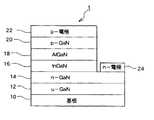
図1には、本実施形態においてGaN系化合物半導体発光素子としてのLED1の基本構成が示されている。LED1は、基板10上に順次GaN層12、Siドープのn型GaN層14、InGaN発光層16、AlGaN層18、p型GaN層20が積層され、p型GaN層20に接してp電極22、n型GaN層14に接してn電極24が形成される構成である。
【0019】
図1に示されたLEDは以下のプロセスにより作製される。すなわち、まず、MOCVD装置にてサファイアc面基板を水素雰囲気中で1100℃、10分間熱処理する。そして、温度を500℃まで降温させ、シランガスとアンモニアガスを100秒間供給して不連続なSiN膜を基板10上に形成する。なお、このプロセスはデバイス中の転位密度を低減させるためのものであり、図ではSiN膜は省略している。次に、同一温度でトリメチルガリウム及びアンモニアガスを供給してGaN層を20nm厚成長させる。温度を1050℃に昇温し、再びトリメチルガリウム及びアンモニアガスを供給してアンドープGaN(u−GaN)層12及びSiドープのn型GaN層14を各2μm厚成長させる。その後、温度を700℃程度まで降温してInGaN発光層16を2nm厚成長させる。目標組成はx=0.15、すなわちIn0.15Ga0.85Nである。発光層16成長後、温度を1000℃まで昇温してAlGaN正孔注入層18を成長させ、さらにp型GaN層20を成長させる。
【0020】
p型GaN層20を成長させた後、ウエハをMOCVD装置から取り出し、Ni10nm厚、Au10nm厚を順次真空蒸着で成長層表面に形成する。5%の酸素を含む窒素ガス雰囲気中で520℃熱処理することで金属膜はp型透明電極22となる。透明電極形成後、全面にフォトレジストを塗布し、n型電極形成のためのエッチングをフォトレジストをマスクとして行う。エッチング深さは、例えば600nm程度である。エッチングで露出したn型GaN層14上にTi5nm厚、Al5nm厚を形成し、窒素ガス雰囲気中で450℃、30分間熱処理してn型電極24を形成する。最後に、基板10の裏面を100μmまで研磨してチップを切り出し、マウントすることでLED1が得られる。
【0021】
図1では、基板10上に一つのLED1が形成されているが、本実施形態では、基板10上にLED1をモノリシックに、かつ二次元アレイ状に複数形成し、各LEDを接続して発光装置(チップ)を構成する。
【0022】
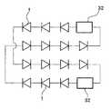
図2には、発光装置の等価回路図が示されている。図2において、2次元アレイ状に形成された発光素子群は同数(図では4個)ずつ2組に分けられ、各組のLED1はそれぞれ直列接続され、2組のLED列は電極(駆動電極)に対して逆極性となるように並列接続される。このようにLED列が直列接続されることにより、各々の駆動電圧が加算された高い電圧でLED1を駆動することができる。また、各LED列はその極性が互いに反対となるように電極に並列接続されているので、電源として交流電源を使用した場合にも、電源の各周期中に必ずどちらかのLED列が発光していることになるので、効率のよい発光を行うことができる。
【0023】
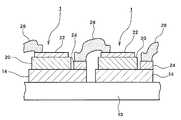
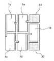
図3には、基板10上にモノリシックに形成された複数のLEDの部分的な平面図が示されている。また、図4は、図3のIV−IV断面図が示されている。図3において、LED1の上面には、図1に示されるようにp電極22及びn電極24が形成されている。隣接するLED1のp電極22とn電極24との間がエアブリッジ配線28により接続され、複数のLED1が直列接続される。
【0024】
図4において、各LED1は説明の都合上簡略的に示されている。すなわち、n−GaN層14、p−GaN層20、p−電極22、n−電極24のみが示されている。実際には図1に示されるようにInGaN発光層16等が存在することは云うまでもない。エアブリッジ配線28は、p電極22からn電極24までを空中を介して接続する。これにより、素子表面に絶縁膜を塗布し、この上に電極を形成してp電極22とn電極24とを電気的に接続する方法に比べ、エッチング溝に沿って電極を配置する必要が無くなるので、配線切れや絶縁膜からn層、p層へ絶縁材料を構成する元素が熱拡散してLED1を劣化させるという問題を回避できる。エアブリッジ配線28は、LED1間のみならずLED1と図示しない電極との間の接続にも使用される。
【0025】
また、図4に示されるように、各LED1は互いに独立し、電気的に絶縁される必要がある。このため、各LED1はサファイア基板10上で分離された構成となっている。サファイアはそれ自身絶縁体であるので、LED1をそれぞれ電気的に分離することができる。このように、サファイア基板10をLEDの電気的な分離を行うための抵抗体として使用することにより、容易かつ確実にLEDの電気的な分離を行うことができる。
【0026】
なお、発光素子としては、pn接合を有するLEDの他、MISとすることもできる。
【0027】
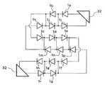
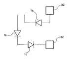
図5には、発光装置の他の等価回路図が示されている。図において、20個のLED1が直列接続されて1つのLEDアレイを形成しており、2つのLEDアレイ(合計40個のLED)が電源に並列に接続されている。LED1の駆動電圧は5Vに設定されており、各LEDアレイの駆動電圧は100Vとなっている。2つのLEDアレイは図2と同様に互いに反対極性となるように電源に並列接続されており、電源の極性がいずれであっても必ずどちらかのLEDアレイが発光することになる。
【0028】
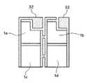
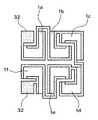
図6には、二次元アレイが具体的に示されている。図2の等価回路図に対応するものである。図において、サファイア基板10上に合計40個のLED1が形成されており、それぞれ20個ずつ2組に分けられ、エアブリッジ配線28により直列接続されて2つのLEDアレイを形成している。より詳細には、各LED1は全て同形の正方形で同サイズであり、1つのLEDアレイは上から6個、7個、7個とそれぞれ直線上に配置され、上から第1列目(6個)と第2列目(7個)は互いに逆向きに形成され、第2列目と第3列目も互いに逆向きに形成される。第1列目と第2列目、第2列目と第3列目は互いに離間して配置されている。これは、後述するように他方のLEDアレイの列が交互に挿入されるためである。第1列目の右端のLED1と第2列目の右端のLED1とはエアブリッジ配線28により接続される。第2列目の左端のLED1と第3列目の左端のLED1もエアブリッジ配線28で接続されてジグザグ配列となる。第1列目の左端のLED1は基板10の左上部に形成された電極(パッド)32にエアブリッジ配線28で接続され、第3列目の右端のLED1は基板10の右下部に形成された電極(パッド)32にエアブリッジ配線28で接続される。2つの電極(パッド)32もLED1と同形の正方形である。他方のLEDアレイは上述した一方のLEDアレイの間隙に互い違いとなるように形成される。すなわち、他方のLEDアレイは上から7個、7個、6個とそれぞれ直線上に配置され、上から第1列目は一方のLEDアレイの第1列目と第2列目の間に形成され、第2列目は一方のLEDアレイの第2列目と第3列目の間に形成され、第3列目は一方のLEDアレイの第3列目の下に形成される。他方のLEDアレイの第1列目と第2列目、及び第2列目と第3列目も互いに逆方向となるように形成され、第1列目の右端のLED1は第2列目の右端のLED1にエアブリッジ配線28で接続され、第2列目の左端のLED1は第3列の左端のLED1にエアブリッジ配線28で接続されてジグザグ状となる。他方のLEDアレイの第1列目の左端のLEDは基板10の左上部に形成された電極32にエアブリッジ配線28で接続され、第3列目の右端のLED1は基板10の右下部に形成された電極32にエアブリッジ配線28で接続される。一方のLEDアレイと他方のLEDアレイの電極32に対する極性は互いに逆である。発光装置(チップ)の全体形状は長方形である。電源が供給される2つの電極32は、長方形の対角位置に離間して形成される点も着目されたい。
【0029】
図7には、図6の回路図が示されている。それぞれのLEDアレイはジグザグ状に屈曲しつつ直列接続され、2つのLEDアレイはジグザグ状の各列が互いの列の間に形成される様子が明らかとなろう。このような配置とすることで、多数のLED1を小さな基板10上に配置することができる。また、40個のLED1に対して電極32が2個でよいので、この点でも基板10の使用効率を向上させることができる。また、各LED1を分離するためにLED1を個別に形成する場合にはウエハをカットして分離する必要があるのに対し、本実施形態では各LED1の分離をエッチングで行うことができるので、LED1の間隔を狭くすることができる。これにより、サファイア基板10の大きさをより小さくすることができる。LED1同士の分離は、フォトレジストや反応性イオンエッチング、ウエットエッチングを併用することでLED1以外の領域を基板10に達するまでエッチング除去することで達成される。各LEDアレイは交互に発光するので、発光効率を向上できるとともに放熱特性も向上させることができる。また、直列接続させるLED1の数を変更すれば、全体としての駆動電圧も変更できる。また、LED1の面積を小さくすると、1つのLED当たりの駆動電圧を高くすることもできる。LED1を20個直列に接続した場合、商用電源(100V、60Hz)で駆動すると、およそ150mWの発光出力を得ることができる。この場合の駆動電流としては20mA程度である。
【0030】
なお、図7から分かるように、2つのLEDアレイをジグザグ状に交互に配列する場合、エアブリッジ配線28に交叉部分34が必然的に発生する。例えば、他方のLEDアレイの第1列目と第2列目を接続する際に、一方のLEDアレイの第1列目と第2列目を接続するための配線部分と交叉する。しかし、本実施形態のエアブリッジ配線28は、上述したように基板10に接着しておらず、基板10から離れて空中を通過するので、交叉部分34においてエアブリッジ配線28同士が接触し、短絡することを容易に回避することができる。エアブリッジ配線28を用いる利点の一つである。エアブリッジ配線28は、例えば以下のようにして形成される。すなわち、全面に2μmの厚さのフォトレジストを塗布し、エアブリッジ配線の形状に穴を開けた後にポストベークする。その上に、真空蒸着でTiを10nm、Auを10nm、この順序で蒸着する。さらにその上の全面に2μm厚さでフォトレジストを再度塗布し、エアブリッジ配線を形成する部分のみに穴を開ける。次いで、TiとAuを電極として電解液中でイオンプレーティング(メッキ)により電極全面に3〜5μmの厚さのAuを付着させる。その後、試料をアセトンに浸し、超音波洗浄によりフォトレジストを溶解除去してエアブリッジ配線28が完成する。
【0031】
このように、複数のLED1を二次元アレイ状に配置することで、基板面積を有効に活用しつつ高駆動電圧、特に商用電源での駆動も可能となるが、二次元アレイのパターンとしてはこの他にも種々のパターンが可能である。一般に、二次元アレイパターンとしては、以下の条件を備えることが望ましい。
【0032】
(1)各LEDに均一に電流を流し、均一な発光を得るためには各LEDの形状、電極位置が同一であることが望ましい。
【0033】
(2)ウエハをカットしてチップにするためには、各LEDの辺は直線であることが望ましい。
【0034】
(3)光取り出し効率を向上させるため、標準的なマウントを使用して周辺からの反射を利用するためにはLEDは平面形状が正方形に近い形状が望ましい。
【0035】
(4)2つの電極(ボンディングパット)の大きさは100μm角程度で、互いに離れていることが望ましい。
【0036】
(5)ウエハ面積の有効利用のため、配線、パッドの占める割合は小さい方が望ましい。
【0037】
もちろん、これらは必須ではなく、例えば各LEDの形状としては平面形状三角形を用いることも可能であろう。各LEDの形状が三角形であっても、これらを組み合わせることで全体形状を略正方形とすることができる。以下、二次元アレイパターンの例をいくつか示す。
【0038】
図8には、合計6個のLED1を二次元に配置した例が示されており、図9にはその回路図が示されている。図8の配置は、基本的には図6の配置と同様であり、合計6個のLEDアレイは同数ずつ2組に分けられ、それぞれ直列接続された3個のLEDから構成される。一方のLEDアレイはジグザグ状に配列され、上から第1列目は1個のLED1、第2列目は2個のLED1が形成される。第1列目のLEDと第2列目の右端のLED1はエアブリッジ配線28で直列接続され、第2列目の2個のLED1もエアブリッジ配線28で直列接続される。基板10の左上部と左下部に電極(パッド)32が形成され、第1列目のLED1は左上部の電極32にエアブリッジ配線で接続され、第2列目の左端のLED1は左下部の電極32に接続される。他方のLEDアレイもジグザグ状に配列され、上から第1列目は2個のLED1、第2列目は1個のLED1が形成される。他方のLEDアレイの第1列目は前記一方のLEDアレイの第1列目と第2列目の間に形成され、他方のLEDアレイの第2列目は前記一方のLEDアレイの第2列目の下方に形成される。第1列目の右端のLED1は第2列目のLED1にエアブリッジ配線28で直列接続され、第1列目の2個のLED1同士もエアブリッジ配線28で直列接続される。第1列目の左端のLED1は左上部の電極32にエアブリッジ配線28で接続され、第2列目のLED1は左下部の電極32にエアブリッジ配線28で接続される。図9から分かるように、この例でも2つのLEDアレイは互いに並列に電極32に接続され、かつ、互いに逆極性となるように接続される。したがって、交流電源を供給した場合、2つのLEDアレイは交互に発光することになる。
【0039】
図10には、合計14個のLEDを二次元配置した例が示されており、図11にはその回路図が示されている。合計14個のLEDアレイは2組に分けられ、それぞれ直列接続された7個のLEDから構成される。一方のLEDアレイはジグザグ状に配列され、上から第1列目は3個のLED1、第2列目は4個のLED1が形成される。第1列目の左端のLEDと第2列目の左端のLED1はエアブリッジ配線28で直列接続され、第1列目の3個のLED同士、及び第2列目の4個のLED1同士もエアブリッジ配線28で直列接続される。基板10の右上部と右下部に電極(パッド)32が形成され、第1列目の右端のLED1は右上部の電極32にエアブリッジ配線で接続され、第2列目の右端のLED1は右下部の電極32に接続される。他方のLEDアレイもジグザグ状に配列され、上から第1列目は4個のLED1、第2列目は3個のLED1が形成される。他方のLEDアレイの第1列目は前記一方のLEDアレイの第1列目と第2列目の間に形成され、他方のLEDアレイの第2列目は前記一方のLEDアレイの第2列目の下方に形成される。第1列目の左端のLED1は第2列目の左端のLED1にエアブリッジ配線28で直列接続される。第1列目の4個のLED1同士、及び第2列目の3個のLED1同士も直列接続される。第1列目の右端のLED1は右上部の電極32にエアブリッジ配線28で接続され、第2列目の右端のLED1は右下部の電極32にエアブリッジ配線28で接続される。図11から分かるように、この例でも2つのLEDアレイは互いに並列に電極32に接続され、かつ、互いに逆極性となるように接続される。したがって、交流電源を供給した場合、2つのLEDアレイは交互に発光することになる。
【0040】
図6、図8、図10の二次元パターンに共通する特徴としては、各LED1が略正方形の同形、同サイズであること、2つの電極(パッド)も略正方形であり、隣接形成されていない(離間形成されている)こと、2つのLEDアレイの組み合わせであること、2つのLEDアレイは屈曲しつつチップ上に互いに交錯するように形成されること、2つのLEDアレイは互いに逆極性となるように電極に接続されること、等である。
【0041】
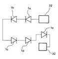
図12には、平面形状が三角形のLEDを二次元配列した場合の例が示されており、図13にはその回路図が示されている。図12において、合計6個のLED1a、1b、1c、1d、1e、1fがその平面形状が三角形状となるように形成されている。LED1aとLED1eが三角形の一辺で対向して2つで略正方形となるように配置され、LED1bと1fが対向して2つで略正方形となるように配置される。また、LED1dと電極32が対向して接続し、LED1cと電極32が対向して接続する。2つの電極32もLEDと同様に平面形状が三角形状であり、同様に略正方形となるように配置される。LED同士の対向する辺はn電極24を構成し、すなわち、対向する2つのLEDはn電極24を共有する。LEDと電極32もn電極接続である。この配置も、上述した例と同様に合計6個のLEDは2組に分けられる。一方のLEDアレイは、LED1a、LED1b、LED1cからなるアレイであり、LED1aのp電極22は電極32にエアブリッジ配線28で接続され、そのn電極24はLED1bのp電極22とエアブリッジ配線28で接続される。LED1bのn電極24はLED1cのp電極22とエアブリッジ配線28で接続される。LED1cのn電極24は電極32に接続される。他方のLEDアレイは、LED1d、LED1e、LED1fから構成され、電極32とLED1fのp電極22はエアブリッジ配線28で接続され、LED1fのn電極24はLED1eのp電極22とエアブリッジ配線28で接続され、LED1eのn電極24とLED1dのp電極22はエアブリッジ配線28で接続され、LED1dのn電極24は電極32に接続される。
【0042】
図13において、一方のLEDアレイを構成するLED1aと他方のLEDアレイを構成するLED1eのn電極が接続されており、一方のLEDアレイを構成するLED1bと他方のLEDアレイを構成するLED1fのn電極が接続されている点にも着目されたい。2組のLEDアレイのいくつかのn電極を共有することで、回路配線を削減することができる。また、この例においても、2つのLEDアレイは並列に電極32に接続され、かつ、互いに逆極性となるように接続される。また、各LEDは同形、同サイズであり、各LEDを一つの辺で対向させるとともに電極32も三角形状とすることでLED及び電極を高密度に形成して必要な基板面積を小さくすることができる。
【0043】
図14には、平面形状が三角形のLEDを二次元配列した他の例が示されており、図15にはその回路図が示されている。この例では、合計16個のLED1a〜1rが二次元形成されている。LED1aと1j、1bと1k、1cと1m、1dと1n、1eと1p、1fと1q、1gと1rがそれぞれ三角形の一つの辺で対向する。対向する辺にはn電極24が共通形成されている。また、LED1iと電極32が対向し、LED1hと電極32が対向する。一方のLEDアレイはLED1a、1b、1c、1d、1e、1f、1g、1hから構成され、他方のLEDアレイはLED1r、1q、1p、1n、1m、1k、1j、1iから構成される。LED1bのn電極24はエアブリッジ配線28によりLED1cのp電極22に接続され、LED1eのn電極24もエアブリッジ配線28によりLED1fのp電極22に接続される。また、LED1qのn電極24もエアブリッジ配線28によりLED1pのp電極22に接続され、LED1mのn電極24もエアブリッジ配線28によりLED1kのp電極22に接続される。図14においても、図12と同様に交叉部分が生じるが、エアブリッジ配線28により短絡を回避できる。また、この例においても2組のLEDアレイのいくつかのn電極24を共有構造とすることで必要な配線を削減している。また、この例においても2つのLEDアレイは並列で互いに逆極性で電極32に接続されており、交流駆動が可能である。図12においては合計6個のLEDの場合、図14においては合計16個のLEDの場合について示したが、他の個数のLEDでも同様に二次元配列できる。本願出願人は、38個のLEDを二次元配列した発光装置も作成している。
【0044】
以上、交流駆動の場合について説明したが、直流駆動も可能であることは言うまでもない。この場合、LEDアレイを互いに逆極性となるように電極に接続するのではなく、直流電源の極性の向きに合わせてLEDアレイを順方向に接続すればよい。複数のLEDを直列接続することで、高電圧駆動が可能である。以下、直流駆動の場合についても説明する。
【0045】
図16には、2個のLEDを直列接続した例が示されており、図17にはその回路図が示されている。各LED1は平面形状が矩形状であり、2個のLED間はエアブリッジ配線28で接続される。電極32は各LED1の近傍に形成されており、電極32とLED1とで長方形の領域を形成する。すなわち、電極32は長方形領域の一部を占有し、長方形領域の他の領域にLED1が形成されている。
【0046】
図18には、合計4個のLEDを二次元配列した例が示されており、図19にはその回路図が示されている。図16のLED1を2個に分割し、それぞれを並列に接続したものである。2個のLEDからなるLEDアレイを2組並列に順方向接続したと云うこともできる。LED1aと1bで一つのLEDアレイを構成し、LED1cと1dでもう一つのLEDアレイを構成する。LED1aとLED1cはp電極22及びn電極24を共有し、LED1bとLED1dもp電極22及びn電極24を共有する。この構成によれば、図16に比べて電流が均一化する効果がある。
【0047】
図20は、合計3個のLEDを二次元配列した例が示されており、図21にはその回路図が示されている。LED1a、1b、1cは同形ではなく、LED1aの一部に電極32が形成されている。LED1aのn電極24とLED1bのp電極はLED1bの上を跨ぐエアブリッジ配線28で接続される。各LEDの形状及び配置を工夫することで、3個のLEDであっても発光装置(チップ)全体の外観形状を略正方形とすることができる。
【0048】
図22には、合計6個のLEDを二次元配列した例が示されており、図23にはその回路図が示されている。各LED1a〜1fは同形、同サイズである。LED1a〜1fは直列接続される。LED1a〜1cは直線上に配置され、LED1d〜1fは他の直線上に配置される。LED1cとLED1dはエアブリッジ配線28で接続される。この例においても、チップの全体形状を略正方形とすることができる。
【0049】
図24には、合計5個のLEDを二次元配列した例が示されており、図25にはその回路図が示されている。LED1a〜1eは同形(長方形)、同サイズである。この例においても、全体形状を略正方形とすることができる。
【0050】
以上、本発明の実施形態について説明したが、本発明はこれに限定されるものではなく種々の変更が可能である。特に、複数の発光素子(LED等)を二次元配置する場合のパターンは上述したパターン以外にも可能である。この場合、隣接する発光素子間で電極を共有して配線を少なくすること、全体形状を正方形あるいは長方形とすること、複数組の発光素子アレイを電極に並列接続すること、交流駆動の場合に複数組の発光素子アレイを互い逆極性とすること、複数組の発光素子アレイをそれぞれジグザグ状に屈曲させて組み合わせること、等が好適である。
【0051】
図26〜図31には、これらの変更例のいくつかが例示されている。図26は交流駆動の場合の二次元配置であり、合計40個のLEDが配置されている。図27はその回路図である。図6と異なる点は、2組のLEDアレイのいくつかがn電極24を共有する点である(図5参照)。例えば、一方のLEDアレイの第1列の右端から2番目に位置するLED(図中αで示す)のn電極24は、他方のLEDアレイの第1列の右端に位置するLED(図中βで示す)のn電極24と共有されている。なお、LEDアレイの端部(図中γ部分)におけるエアブリッジ配線28は、交叉させることなく共通形成されている。
【0052】
図28は、交流駆動の場合の二次元配置であり、合計14個のLEDが配置されている。図29はその回路図である。図10と異なる点は、2組のLEDアレイのいくつかがn電極24を共有する点である。例えば、一方のLEDアレイの第1列の左端のLED(図中αで示す)のn電極24は、他方のLEDアレイの第1列の右端から2番目に位置するLED(図中βで示す)のn電極24と共有されている。また、端部(図中γ部分)におけるエアブリッジ配線28は共通形成されている。
【0053】
図30は、交流駆動の場合の二次元配置であり、合計6個のLEDが配置されている。図31はその回路図である。この例においても、端部(γ部)のエアブリッジ配線28が共通形成されている。この構成も、一方のLEDアレイにおけるn電極24と他方のLEDアレイにおけるn電極24が共有されていると云うことができる。
【0054】
【発明の効果】
以上説明したように、本発明によれば、高い駆動電圧で駆動し発光させることができる。
【図面の簡単な説明】
【図1】 発光素子(LED)の基本構成図である。
【図2】 発光装置の等価回路図である。
【図3】 2個のLEDの平面図である。
【図4】 図3のIV−IV断面図である。
【図5】 発光装置の他の等価回路図である。
【図6】 40個のLEDを二次元配列した説明図である。
【図7】 図6の回路図である。
【図8】 6個のLEDを二次元配列した説明図である。
【図9】 図8の回路図である。
【図10】 14個のLEDを二次元配列した説明図である。
【図11】 図10の回路図である。
【図12】 6個のLEDを二次元配列した説明図である。
【図13】 図12の回路図である。
【図14】 16個のLEDを二次元配列した説明図である。
【図15】 図14の回路図である。
【図16】 2個のLEDを配列した説明図である。
【図17】 図16の回路図である。
【図18】 4個のLEDを二次元配列した説明図である。
【図19】 図18の回路図である。
【図20】 3個のLEDを二次元配列した説明図である。
【図21】 図20の回路図である。
【図22】 6個のLEDを二次元配列した説明図である。
【図23】 図22の回路図である。
【図24】 5個のLEDを二次元配列した説明図である。
【図25】 図24の回路図である。
【図26】 他の二次元配置説明図である。
【図27】 図26の回路図である。
【図28】 他の二次元配置説明図である。
【図29】 図28の回路図である。
【図30】 他の二次元配置説明図である。
【図31】 図30の回路図である。
【符号の説明】
10 基板(ウエハ)、12 u−GaN層、14 n型GaN層、16 InGaN発光層、18 AlGaN層、20 p−GaN層、22 p−電極、24 n−電極。[0001]
BACKGROUND OF THE INVENTION
The present invention relates to a light emitting device in which a plurality of light emitting elements are formed on a substrate.
[0002]
[Prior art]
When a light emitting means such as a light emitting element (LED) is used for a display application or the like, the use conditions are a drive voltage of about 1 to 4 V and a drive current of about 20 mA. By the way, with the recent development of short-wavelength LEDs using GaN-based compound semiconductors and the practical use of solid-state light sources such as full color and white, it has been studied to gradually apply LEDs to lighting applications. When the LED is applied to lighting applications, there is a situation in which the LED is used under conditions different from the use conditions of the drive voltage of 1 to 4 V and the drive current of 20 mA. For this reason, a device has been devised in which a large current is passed through the LED to increase the light emission output. In order to flow a large current, it is necessary to increase the pn junction area of the LED and reduce the current density.
[0003]
[Problems to be solved by the invention]
When using an LED as a light source for illumination, it is convenient that an alternating current is used as a power source and it can be used at a driving voltage of 100 V or more. If the same light output is obtained by applying the same power, the power loss can be reduced by applying a high voltage while maintaining a low current value. However, in the conventional LED, the drive voltage cannot always be sufficiently increased.
[0004]
The present invention has been made in view of the above-described problems of the prior art, and an object thereof is to provide a light-emitting device that can operate at a high driving voltage.
[0005]
[Means for Solving the Problems]
In order to achieve the above object, the present invention is a light emitting device in which a plurality of GaN-based light emitting diode elements are formed on an insulating substrate,The plurality of light emitting diode elements are two-dimensionally arranged on the insulating substrate, and the plurality of light emitting diode elements are divided into the first group and the second group by the same number, and the first group and the second group are respectively Among the light-emitting diode elements constituting the first set, the first set and the second set are connected in parallel so as to have opposite polarities to the two AC power supply electrodes. Of at least one of the light-emitting diode elements excluding the light-emitting diode element located at the end and adjacent to any one of the light-emitting diode elements constituting the second set The negative electrode of the light emitting diode element is shared and electrically connected It is characterized by that.
[0015]
Thus, in the present invention, a plurality of light emitting elements are formed monolithically, that is, on the same substrate, and these are connected in series, thereby enabling a high driving voltage. Direct current drive is possible by connecting a plurality of light emitting elements in one direction, but the plurality of light emitting elements are divided into two sets, and each set of light emitting elements (light emitting element array) is connected to electrodes so as to have opposite polarities. By connecting, AC driving is also possible. The number of each set may be the same or different.
[0016]
Although there are various methods for two-dimensionally arranging a plurality of light emitting elements, it is desirable to make the area occupied by the substrate as small as possible. For example, two sets of light-emitting element arrays are arranged in a zigzag shape, that is, a plurality of light-emitting elements are arranged on a bent straight line, and the light-emitting element arrays are alternately arranged, so that a large number of light-emitting element arrays can be used effectively. A light emitting element can be connected. By arranging two sets of light emitting element arrays in a staggered manner, there may be a crossing portion of the wiring, but a short circuit at the crossing portion can be effectively prevented by connecting the light emitting elements with an air bridge wiring. Although the shape of the light emitting element and the electrode is arbitrary, for example, when the planar shape is formed to be approximately square, the overall shape is also approximately square, and a standard mount structure can be used. Even when the light emitting element and the electrode are other than a square, for example, a triangle, a standard mount structure can be similarly used if a substantially square is formed as a whole by combining these triangles.
[0017]
DETAILED DESCRIPTION OF THE INVENTION
Hereinafter, embodiments of the present invention will be described with reference to the drawings.
[0018]
FIG. 1 shows a basic configuration of an
[0019]
The LED shown in FIG. 1 is manufactured by the following process. That is, first, a sapphire c-plane substrate is heat-treated in a hydrogen atmosphere at 1100 ° C. for 10 minutes by a MOCVD apparatus. Then, the temperature is lowered to 500 ° C., silane gas and ammonia gas are supplied for 100 seconds, and a discontinuous SiN film is formed on the
[0020]
After the p-
[0021]
In FIG. 1, one
[0022]
FIG. 2 shows an equivalent circuit diagram of the light emitting device. In FIG. 2, the light emitting element groups formed in a two-dimensional array are divided into two sets of the same number (four in the figure), each set of
[0023]
FIG. 3 shows a partial plan view of a plurality of LEDs monolithically formed on the
[0024]
In FIG. 4, each
[0025]
Further, as shown in FIG. 4, each
[0026]
In addition, as a light emitting element, it can also be set to MIS besides LED which has a pn junction.
[0027]
FIG. 5 shows another equivalent circuit diagram of the light emitting device. In the figure, 20
[0028]
FIG. 6 specifically shows a two-dimensional array. This corresponds to the equivalent circuit diagram of FIG. In the figure, a total of 40
[0029]
FIG. 7 shows a circuit diagram of FIG. It will be apparent that the respective LED arrays are connected in series while being bent in a zigzag manner, and two LED arrays are formed in a zigzag manner between each other. With such an arrangement, a large number of
[0030]
As can be seen from FIG. 7, when two LED arrays are alternately arranged in a zigzag shape, a crossing
[0031]
Thus, by arranging a plurality of
[0032]
(1) It is desirable that the shape and the electrode position of each LED be the same in order to pass a current uniformly to each LED and obtain uniform light emission.
[0033]
(2) In order to cut the wafer into chips, it is desirable that the sides of each LED be straight.
[0034]
(3) In order to improve the light extraction efficiency, in order to use reflection from the periphery using a standard mount, the LED preferably has a planar shape close to a square.
[0035]
(4) The size of the two electrodes (bonding pads) is about 100 μm square, and it is desirable that they are separated from each other.
[0036]
(5) In order to effectively use the wafer area, it is desirable that the proportion of wiring and pads is small.
[0037]
Of course, these are not essential, and for example, it is possible to use a planar shape triangle as the shape of each LED. Even if each LED has a triangular shape, the overall shape can be made substantially square by combining them. Hereinafter, some examples of the two-dimensional array pattern are shown.
[0038]
FIG. 8 shows an example in which a total of six
[0039]
FIG. 10 shows an example in which a total of 14 LEDs are two-dimensionally arranged, and FIG. 11 shows a circuit diagram thereof. A total of 14 LED arrays are divided into 2 sets, each consisting of 7 LEDs connected in series. One LED array is arranged in a zigzag shape, and from the top, three
[0040]
The common features of the two-dimensional patterns of FIGS. 6, 8, and 10 are that each
[0041]
FIG. 12 shows an example in which LEDs having a triangular planar shape are two-dimensionally arranged, and FIG. 13 shows a circuit diagram thereof. In FIG. 12, a total of six
[0042]
In FIG. 13, the
[0043]
FIG. 14 shows another example in which LEDs having a triangular planar shape are two-dimensionally arranged, and FIG. 15 shows a circuit diagram thereof. In this example, a total of 16
[0044]
Although the case of AC driving has been described above, it goes without saying that DC driving is also possible. In this case, the LED array may be connected in the forward direction according to the polarity direction of the DC power supply, instead of connecting the LED array to the electrodes so as to have opposite polarities. High voltage driving is possible by connecting a plurality of LEDs in series. Hereinafter, the case of direct current drive will also be described.
[0045]
FIG. 16 shows an example in which two LEDs are connected in series, and FIG. 17 shows a circuit diagram thereof. Each
[0046]
FIG. 18 shows an example in which a total of four LEDs are two-dimensionally arranged, and FIG. 19 shows a circuit diagram thereof. LED1 of FIG. 16 is divided | segmented into two, and each is connected in parallel. It can also be said that two sets of LED arrays composed of two LEDs are connected in a forward direction in parallel. The
[0047]
FIG. 20 shows an example in which a total of three LEDs are two-dimensionally arranged, and FIG. 21 shows a circuit diagram thereof. The
[0048]
FIG. 22 shows an example in which a total of six LEDs are two-dimensionally arranged, and FIG. 23 shows a circuit diagram thereof. Each
[0049]
FIG. 24 shows an example in which a total of five LEDs are two-dimensionally arranged, and FIG. 25 shows a circuit diagram thereof. The
[0050]
As mentioned above, although embodiment of this invention was described, this invention is not limited to this, A various change is possible. In particular, the pattern in the case where a plurality of light emitting elements (LEDs, etc.) are two-dimensionally arranged is possible in addition to the patterns described above. In this case, the electrodes are shared between adjacent light emitting elements to reduce wiring, the overall shape is square or rectangular, a plurality of sets of light emitting element arrays are connected in parallel to the electrodes, and plural in the case of AC drive. It is preferable that the sets of light emitting element arrays have opposite polarities, the plurality of sets of light emitting element arrays are combined in a zigzag manner, and the like.
[0051]
26 to 31 illustrate some of these modifications. FIG. 26 shows a two-dimensional arrangement in the case of AC driving, in which a total of 40 LEDs are arranged. FIG. 27 is a circuit diagram thereof. The difference from FIG. 6 is that some of the two sets of LED arrays share the n-electrode 24 (see FIG. 5). For example, the
[0052]
FIG. 28 shows a two-dimensional arrangement in the case of AC driving, in which a total of 14 LEDs are arranged. FIG. 29 is a circuit diagram thereof. A difference from FIG. 10 is that some of the two sets of LED arrays share the n-
[0053]
FIG. 30 shows a two-dimensional arrangement in the case of AC driving, in which a total of six LEDs are arranged. FIG. 31 is a circuit diagram thereof. Also in this example, the
[0054]
【The invention's effect】
As described above, according to the present invention, it is possible to drive and emit light with a high driving voltage.
[Brief description of the drawings]
FIG. 1 is a basic configuration diagram of a light emitting element (LED).
FIG. 2 is an equivalent circuit diagram of the light emitting device.
FIG. 3 is a plan view of two LEDs.
4 is a cross-sectional view taken along the line IV-IV in FIG.
FIG. 5 is another equivalent circuit diagram of the light emitting device.
FIG. 6 is an explanatory diagram in which 40 LEDs are two-dimensionally arranged.
7 is a circuit diagram of FIG. 6. FIG.
FIG. 8 is an explanatory diagram in which six LEDs are two-dimensionally arranged.
9 is a circuit diagram of FIG. 8. FIG.
FIG. 10 is an explanatory diagram in which 14 LEDs are two-dimensionally arranged.
11 is a circuit diagram of FIG.
FIG. 12 is an explanatory diagram in which six LEDs are two-dimensionally arranged.
FIG. 13 is a circuit diagram of FIG.
FIG. 14 is an explanatory diagram in which 16 LEDs are two-dimensionally arranged.
FIG. 15 is a circuit diagram of FIG. 14;
FIG. 16 is an explanatory diagram in which two LEDs are arranged.
FIG. 17 is a circuit diagram of FIG. 16;
FIG. 18 is an explanatory diagram in which four LEDs are two-dimensionally arranged.
FIG. 19 is a circuit diagram of FIG. 18;
FIG. 20 is an explanatory diagram in which three LEDs are two-dimensionally arranged.
FIG. 21 is a circuit diagram of FIG. 20;
FIG. 22 is an explanatory diagram in which six LEDs are two-dimensionally arranged.
FIG. 23 is a circuit diagram of FIG. 22;
FIG. 24 is an explanatory diagram in which five LEDs are two-dimensionally arranged.
25 is a circuit diagram of FIG. 24. FIG.
FIG. 26 is another explanatory diagram of a two-dimensional arrangement.
FIG. 27 is a circuit diagram of FIG. 26;
FIG. 28 is an explanatory diagram of another two-dimensional arrangement.
29 is a circuit diagram of FIG. 28. FIG.
FIG. 30 is another explanatory diagram of two-dimensional arrangement.
31 is a circuit diagram of FIG. 30. FIG.
[Explanation of symbols]
10 substrate (wafer), 12 u-GaN layer, 14 n-type GaN layer, 16 InGaN light emitting layer, 18 AlGaN layer, 20 p-GaN layer, 22 p-electrode, 24 n-electrode.
Claims (1)
Translated fromJapanese前記複数の発光ダイオード素子は同数ずつ第1の組と第2の組に分けられ、第1の組と第2の組はそれぞれジグザグ状に互い違いに配置され、第1の組と第2の組は2個の交流電源用電極に互いに反対極性となるように並列接続され、
前記第1の組を構成する発光ダイオード素子のうちの、少なくとも、端部に位置する発光ダイオード素子を除くいずれかの発光ダイオード素子の負電極と、前記第2の組を構成する発光ダイオード素子のうちの、前記いずれかの発光ダイオード素子に隣接する発光ダイオード素子の負電極とが共有されて電気的に接続されることを特徴とする発光装置。A light emitting device in which a plurality of GaN-based light emitting diode elements are formed on aninsulating substrate ,wherein the plurality of light emitting diode elements are two-dimensionally arranged on the insulating substrate,
The plurality of light emitting diode elements are divided into the first group and the second group by the same number, and the first group and the second group are alternately arranged in a zigzag shape, and the first group and the second group are arranged. Are connected in parallel to the two AC power supply electrodes so as to have opposite polarities,
Of the light emitting diode elements constituting the first group, at least the negative electrode of any one of the light emitting diode elements excluding the light emitting diode element located at the end, and the light emitting diode elements constituting the second group A light emitting device, wherein a negative electrode of a light emitting diode element adjacent to any one of the light emitting diode elements is shared and electrically connected .
Priority Applications (37)
| Application Number | Priority Date | Filing Date | Title |
|---|---|---|---|
| JP2002249957AJP3822545B2 (en) | 2002-04-12 | 2002-08-29 | Light emitting device |
| CNB038206226ACN100421266C (en) | 2002-08-29 | 2003-08-28 | Light emitting device having a plurality of light emitting elements |
| KR20057002667AKR100697803B1 (en) | 2002-08-29 | 2003-08-28 | Light emitting device having a plurality of light emitting elements |
| EP20090000561EP2101355A1 (en) | 2002-08-29 | 2003-08-28 | Light-emitting device having light-emitting elements |
| PCT/JP2003/010922WO2004023568A1 (en) | 2002-08-29 | 2003-08-28 | Light-emitting device having light-emitting elements |
| RU2005103616ARU2295174C2 (en) | 2002-08-29 | 2003-08-28 | Light-emitting device incorporating light-emitting components (alternatives) |
| ES03794115TES2362407T3 (en) | 2002-08-29 | 2003-08-28 | LIGHTING ISSUER DEVICE PROVIDED BY LIGHTING ISSUING DIODES. |
| EP09014624.2AEP2154722B1 (en) | 2002-08-29 | 2003-08-28 | Light-emitting device having light-emitting diodes |
| CNB2007101029609ACN100570883C (en) | 2002-08-29 | 2003-08-28 | Lighting device with multiple light emitting elements |
| EP07118916.1AEP1892764B1 (en) | 2002-08-29 | 2003-08-28 | Light-emitting device having light-emitting diodes |
| EP18150767.4AEP3389094A1 (en) | 2002-08-29 | 2003-08-28 | Light-emitting device having light-emitting elements |
| AT03794115TATE500616T1 (en) | 2002-08-29 | 2003-08-28 | LIGHT EMITTING COMPONENT WITH LIGHT EMITTING DIODES |
| EP09014623.4AEP2154721B1 (en) | 2002-08-29 | 2003-08-28 | Light-emitting device having light-emitting diodes |
| EP20090014620EP2157609A3 (en) | 2002-08-29 | 2003-08-28 | Light-emitting device having light-emitting diodes |
| EP20030794115EP1553641B1 (en) | 2002-08-29 | 2003-08-28 | Light-emitting device having light-emitting diodes |
| EP20090014625EP2149907A3 (en) | 2002-08-29 | 2003-08-28 | Light-emitting device having light-emitting diodes |
| EP20090014622EP2149906A3 (en) | 2002-08-29 | 2003-08-28 | Light-emitting device having light-emitting diodes |
| EP20090014621EP2149905A3 (en) | 2002-08-29 | 2003-08-28 | Light-emitting device having light-emitting diodes |
| DE60336252TDE60336252D1 (en) | 2002-08-29 | 2003-08-28 | LIGHT-EMITTING COMPONENT WITH LIGHT-EMITTING DIODES |
| US10/525,998US7417259B2 (en) | 2002-08-29 | 2003-08-28 | Light-emitting device having light-emitting elements |
| TW92123908ATWI280672B (en) | 2002-08-29 | 2003-08-29 | Light-emitting device having light-emitting elements |
| US11/705,205US7956367B2 (en) | 2002-08-29 | 2007-02-12 | Light-emitting device having light-emitting elements connected in series |
| US12/060,693US8129729B2 (en) | 2002-08-29 | 2008-04-01 | Light emitting device having light emitting elements and an air bridge line |
| US12/139,927US7897982B2 (en) | 2002-08-29 | 2008-06-16 | Light emitting device having common N-electrode |
| US12/352,296US8084774B2 (en) | 2002-08-29 | 2009-01-12 | Light emitting device having light emitting elements |
| US12/352,280US7615793B2 (en) | 2002-08-29 | 2009-01-12 | AC driven light—emitting device |
| US12/352,271US7569861B2 (en) | 2002-08-29 | 2009-01-12 | Light emitting device having light emitting elements |
| US12/352,240US8097889B2 (en) | 2002-08-29 | 2009-01-12 | Light emitting device having light emitting elements with a shared electrode |
| US12/478,456US7667237B2 (en) | 2002-08-29 | 2009-06-04 | Light emitting device having light emitting elements |
| US12/479,380US7646031B2 (en) | 2002-08-29 | 2009-06-05 | Light emitting device having light emitting elements |
| US12/652,518US8680533B2 (en) | 2002-08-29 | 2010-01-05 | Light-emitting device having light-emitting elements with a shared electrode |
| US12/958,947US8735918B2 (en) | 2002-08-29 | 2010-12-02 | Light-emitting device having light-emitting elements with polygonal shape |
| US13/584,140US20120305951A1 (en) | 2002-08-29 | 2012-08-13 | Light-emitting device having light-emitting elements |
| US13/610,819US8735911B2 (en) | 2002-08-29 | 2012-09-11 | Light emitting device having shared electrodes |
| US13/890,878US9947717B2 (en) | 2002-08-29 | 2013-05-09 | Light-emitting device having light-emitting elements and electrode spaced apart from the light emitting element |
| US14/583,476US20150108497A1 (en) | 2002-08-29 | 2014-12-26 | Light-emitting device having light-emitting elements |
| US15/430,440US20170154922A1 (en) | 2002-08-29 | 2017-02-10 | Light-emitting device having an array of light-emitting elements |
Applications Claiming Priority (2)
| Application Number | Priority Date | Filing Date | Title |
|---|---|---|---|
| JP2002110760 | 2002-04-12 | ||
| JP2002249957AJP3822545B2 (en) | 2002-04-12 | 2002-08-29 | Light emitting device |
Related Child Applications (1)
| Application Number | Title | Priority Date | Filing Date |
|---|---|---|---|
| JP2006117739ADivisionJP4195041B2 (en) | 2002-04-12 | 2006-04-21 | Light emitting device |
Publications (2)
| Publication Number | Publication Date |
|---|---|
| JP2004006582A JP2004006582A (en) | 2004-01-08 |
| JP3822545B2true JP3822545B2 (en) | 2006-09-20 |
Family
ID=30446964
Family Applications (1)
| Application Number | Title | Priority Date | Filing Date |
|---|---|---|---|
| JP2002249957AExpired - LifetimeJP3822545B2 (en) | 2002-04-12 | 2002-08-29 | Light emitting device |
Country Status (1)
| Country | Link |
|---|---|
| JP (1) | JP3822545B2 (en) |
Cited By (4)
| Publication number | Priority date | Publication date | Assignee | Title |
|---|---|---|---|---|
| JP2008211255A (en)* | 2002-04-12 | 2008-09-11 | Seoul Semiconductor Co Ltd | Light-emitting device |
| US7667237B2 (en) | 2002-08-29 | 2010-02-23 | Seoul Semiconductor Co., Ltd. | Light emitting device having light emitting elements |
| WO2011099771A3 (en)* | 2010-02-12 | 2011-12-29 | Seoul Opto Device Co., Ltd. | Light emitting diode chip having distributed bragg reflector and method of fabricating the same |
| KR101448153B1 (en) | 2008-06-25 | 2014-10-08 | 삼성전자주식회사 | A multi-chip package for a light-emitting diode and a light-emitting diode |
Families Citing this family (101)
| Publication number | Priority date | Publication date | Assignee | Title |
|---|---|---|---|---|
| US7213942B2 (en) | 2002-10-24 | 2007-05-08 | Ac Led Lighting, L.L.C. | Light emitting diodes for high AC voltage operation and general lighting |
| BRPI0507223A (en)* | 2004-02-25 | 2007-06-19 | Michael Miskin | ac led light and methods and ac led targeting apparatus |
| KR100655894B1 (en) | 2004-05-06 | 2006-12-08 | 서울옵토디바이스주식회사 | Wavelength conversion light emitting device with excellent color temperature and color rendering |
| KR100658700B1 (en) | 2004-05-13 | 2006-12-15 | 서울옵토디바이스주식회사 | Light emitting device combining RGB light emitting element and phosphor |
| KR100665299B1 (en) | 2004-06-10 | 2007-01-04 | 서울반도체 주식회사 | Emitting material |
| US8308980B2 (en) | 2004-06-10 | 2012-11-13 | Seoul Semiconductor Co., Ltd. | Light emitting device |
| JP4841550B2 (en) | 2004-06-30 | 2011-12-21 | ソウル オプト デバイス カンパニー リミテッド | LIGHT EMITTING ELEMENT, ITS MANUFACTURING METHOD, AND LIGHT EMITTING DEVICE USING THE SAME |
| TW200501464A (en) | 2004-08-31 | 2005-01-01 | Ind Tech Res Inst | LED chip structure with AC loop |
| KR101216938B1 (en) | 2004-10-28 | 2012-12-31 | 서울반도체 주식회사 | Luminous element having arrayed cells and method of manufacturing thereof and luminous apparatus using the same |
| JP2008523637A (en) | 2004-12-14 | 2008-07-03 | ソウル オプト−デバイス カンパニー リミテッド | Light emitting device having a plurality of light emitting cells and package mounting the same |
| KR101138974B1 (en) | 2005-01-07 | 2012-04-25 | 서울옵토디바이스주식회사 | Luminous element and method of manufacturing thereof |
| US7221044B2 (en) | 2005-01-21 | 2007-05-22 | Ac Led Lighting, L.L.C. | Heterogeneous integrated high voltage DC/AC light emitter |
| KR101138944B1 (en)* | 2005-01-26 | 2012-04-25 | 서울옵토디바이스주식회사 | Light emitting device having a plurality of light emitting cells connected in series and method of fabricating the same |
| US7535028B2 (en) | 2005-02-03 | 2009-05-19 | Ac Led Lighting, L.Lc. | Micro-LED based high voltage AC/DC indicator lamp |
| KR101142939B1 (en) | 2005-02-23 | 2012-05-10 | 서울반도체 주식회사 | Light emitting device |
| DE102005009060A1 (en)* | 2005-02-28 | 2006-09-07 | Osram Opto Semiconductors Gmbh | Module with radiation-emitting semiconductor bodies |
| CN100464111C (en)* | 2005-03-04 | 2009-02-25 | 吕大明 | AC LED lighting lamp |
| JP5059739B2 (en) | 2005-03-11 | 2012-10-31 | ソウル セミコンダクター カンパニー リミテッド | Light emitting diode package having an array of light emitting cells connected in series |
| KR101248513B1 (en)* | 2005-03-29 | 2013-04-04 | 서울반도체 주식회사 | High flux led lamp mounting a led having an array of light emitting cells coupled in series |
| JP4995432B2 (en)* | 2005-05-18 | 2012-08-08 | ローム株式会社 | Semiconductor light emitting device |
| US8476648B2 (en) | 2005-06-22 | 2013-07-02 | Seoul Opto Device Co., Ltd. | Light emitting device and method of manufacturing the same |
| US8188687B2 (en)* | 2005-06-28 | 2012-05-29 | Seoul Opto Device Co., Ltd. | Light emitting device for AC power operation |
| KR100599012B1 (en) | 2005-06-29 | 2006-07-12 | 서울옵토디바이스주식회사 | Light Emitting Diode Having Thermally Conductive Substrate And Method Of Manufacturing The Same |
| KR100608920B1 (en) | 2005-06-30 | 2006-08-03 | 서울옵토디바이스주식회사 | Wiring shape of light emitting device in which a plurality of light emitting cells are arranged |
| KR100616415B1 (en)* | 2005-08-08 | 2006-08-29 | 서울옵토디바이스주식회사 | AC light emitting device |
| US8901575B2 (en) | 2005-08-09 | 2014-12-02 | Seoul Viosys Co., Ltd. | AC light emitting diode and method for fabricating the same |
| KR100758541B1 (en) | 2005-08-22 | 2007-09-13 | 서울옵토디바이스주식회사 | Light emitting diodes having light emitting cells arranged in a matrix and a method of manufacturing the same |
| KR100634307B1 (en)* | 2005-08-10 | 2006-10-16 | 서울옵토디바이스주식회사 | Light emitting device and manufacturing method thereof |
| JP5193048B2 (en)* | 2005-09-30 | 2013-05-08 | ソウル オプト デバイス カンパニー リミテッド | Light emitting device having vertically stacked light emitting diodes |
| KR100721454B1 (en)* | 2005-11-10 | 2007-05-23 | 서울옵토디바이스주식회사 | Light emitting device for alternating current having photonic crystal structure and method for manufacturing same |
| KR101258397B1 (en) | 2005-11-11 | 2013-04-30 | 서울반도체 주식회사 | Copper-Alkaline-Earth-Silicate mixed crystal phosphors |
| JP4728788B2 (en)* | 2005-12-05 | 2011-07-20 | ローム株式会社 | Semiconductor light emitting device |
| KR101158073B1 (en)* | 2005-12-13 | 2012-06-22 | 서울옵토디바이스주식회사 | Light emitting device having arrayed cells |
| KR101055772B1 (en) | 2005-12-15 | 2011-08-11 | 서울반도체 주식회사 | Light emitting device |
| TW200739952A (en) | 2005-12-22 | 2007-10-16 | Rohm Co Ltd | Light emitting device and illumination instrument |
| KR101203138B1 (en) | 2006-01-12 | 2012-11-20 | 서울옵토디바이스주식회사 | Luminous device and the method therefor |
| KR100875443B1 (en) | 2006-03-31 | 2008-12-23 | 서울반도체 주식회사 | Light emitting device |
| JP2007281081A (en)* | 2006-04-04 | 2007-10-25 | Rohm Co Ltd | Semiconductor light emitting device |
| JP4736926B2 (en)* | 2006-04-21 | 2011-07-27 | パナソニック電工株式会社 | EL lighting panel |
| KR101258227B1 (en) | 2006-08-29 | 2013-04-25 | 서울반도체 주식회사 | Light emitting device |
| KR100765240B1 (en)* | 2006-09-30 | 2007-10-09 | 서울옵토디바이스주식회사 | LED package having light emitting cells of different sizes and light emitting device using the same |
| KR101158079B1 (en) | 2006-12-22 | 2012-07-20 | 서울옵토디바이스주식회사 | A luminous element having numerous cells |
| DE112007002696T5 (en) | 2006-12-26 | 2009-11-05 | Seoul Opto Device Co. Ltd., Ansan | Light emitting device |
| EP2111640B1 (en) | 2007-01-22 | 2019-05-08 | Cree, Inc. | Fault tolerant light emitter and method of fabricating the same |
| TWI440210B (en) | 2007-01-22 | 2014-06-01 | Cree Inc | Illumination device using external interconnection array of light-emitting device and manufacturing method thereof |
| KR20110110867A (en)* | 2007-03-13 | 2011-10-07 | 서울옵토디바이스주식회사 | AC LED |
| KR100974923B1 (en) | 2007-03-19 | 2010-08-10 | 서울옵토디바이스주식회사 | Light emitting diode |
| KR100856230B1 (en) | 2007-03-21 | 2008-09-03 | 삼성전기주식회사 | Light emitting device, manufacturing method and monolithic light emitting diode array |
| KR100872248B1 (en) | 2007-06-11 | 2008-12-05 | 삼성전기주식회사 | AC drive light emitting device |
| KR100843402B1 (en) | 2007-06-22 | 2008-07-03 | 삼성전기주식회사 | LED drive circuit and LED array device |
| RU2467051C2 (en) | 2007-08-22 | 2012-11-20 | Сеул Семикондактор Ко., Лтд. | Luminophores based on nonstoichiometric tetragonal silicates of copper and alkali-earth metal and method for production thereof |
| KR101055769B1 (en) | 2007-08-28 | 2011-08-11 | 서울반도체 주식회사 | Light-emitting device adopting non-stoichiometric tetra-alkaline earth silicate phosphor |
| KR100889956B1 (en)* | 2007-09-27 | 2009-03-20 | 서울옵토디바이스주식회사 | AC Light Emitting Diode |
| KR100928259B1 (en) | 2007-10-15 | 2009-11-24 | 엘지전자 주식회사 | Light emitting device and manufacturing method thereof |
| KR101423723B1 (en) | 2007-10-29 | 2014-08-04 | 서울바이오시스 주식회사 | Light emitting diode package |
| WO2009088084A1 (en) | 2008-01-11 | 2009-07-16 | Rohm Co., Ltd. | Semiconductor light emitting device |
| KR100956224B1 (en) | 2008-06-30 | 2010-05-04 | 삼성엘이디 주식회사 | LED drive circuit and LED array device |
| KR101025972B1 (en) | 2008-06-30 | 2011-03-30 | 삼성엘이디 주식회사 | AC drive light emitting device |
| KR101603773B1 (en)* | 2009-01-07 | 2016-03-17 | 서울바이오시스 주식회사 | Light emitting diode having plurality of light emitting cells |
| WO2010050694A2 (en)* | 2008-10-29 | 2010-05-06 | 서울옵토디바이스주식회사 | Light emitting diode |
| KR101017395B1 (en) | 2008-12-24 | 2011-02-28 | 서울옵토디바이스주식회사 | Light emitting device having a plurality of light emitting cells and method of manufacturing same |
| KR101557362B1 (en) | 2008-12-31 | 2015-10-08 | 서울바이오시스 주식회사 | A light emitting device having a plurality of non-polar light emitting cells and a method of manufacturing the same |
| KR101533817B1 (en) | 2008-12-31 | 2015-07-09 | 서울바이오시스 주식회사 | A light emitting device having a plurality of non-polar light emitting cells and a method of manufacturing the same |
| DE102009030205A1 (en) | 2009-06-24 | 2010-12-30 | Litec-Lp Gmbh | Phosphors with Eu (II) -doped silicate luminophores |
| KR101055762B1 (en) | 2009-09-01 | 2011-08-11 | 서울반도체 주식회사 | Light-emitting device employing a light-emitting material having an oxyosilicate light emitter |
| KR101138975B1 (en)* | 2009-09-15 | 2012-04-25 | 서울옵토디바이스주식회사 | Ac light emitting diode having full-wave lihgt emitting cell and half-wave light emitting cell |
| US9324691B2 (en)* | 2009-10-20 | 2016-04-26 | Epistar Corporation | Optoelectronic device |
| DE102009051129A1 (en) | 2009-10-28 | 2011-06-01 | Osram Opto Semiconductors Gmbh | Optoelectronic component and method for producing an optoelectronic component |
| KR101203139B1 (en)* | 2010-01-06 | 2012-11-20 | 서울옵토디바이스주식회사 | Luminous element having arrayed cells |
| EP2367203A1 (en)* | 2010-02-26 | 2011-09-21 | Samsung LED Co., Ltd. | Semiconductor light emitting device having multi-cell array and method for manufacturing the same |
| WO2011115361A2 (en)* | 2010-03-15 | 2011-09-22 | 서울옵토디바이스주식회사 | Light-emitting device having a plurality of light-emitting cells |
| TWI446527B (en)* | 2010-07-02 | 2014-07-21 | Epistar Corp | Optoelectronic component |
| US9171883B2 (en)* | 2010-08-30 | 2015-10-27 | Epistar Corporation | Light emitting device |
| JP2012054447A (en)* | 2010-09-02 | 2012-03-15 | Seiwa Electric Mfg Co Ltd | Semiconductor light-emitting element, light-emitting device, lighting unit, and display unit |
| US9070851B2 (en) | 2010-09-24 | 2015-06-30 | Seoul Semiconductor Co., Ltd. | Wafer-level light emitting diode package and method of fabricating the same |
| JP2011055007A (en)* | 2010-12-13 | 2011-03-17 | Seoul Opto Devices Co Ltd | Ac-driven light emitting diode |
| KR101259998B1 (en)* | 2011-03-31 | 2013-05-06 | 서울옵토디바이스주식회사 | Light emitting diode |
| KR101106139B1 (en)* | 2011-04-04 | 2012-01-20 | 서울옵토디바이스주식회사 | Flip bonded light emitting diode having an extended metal reflective layer and a method of manufacturing the same |
| KR101115538B1 (en)* | 2011-04-04 | 2012-02-28 | 서울옵토디바이스주식회사 | Luminous device and the method therefor |
| KR101115540B1 (en)* | 2011-06-30 | 2012-02-28 | 서울옵토디바이스주식회사 | Light emitting diode package |
| KR101221336B1 (en)* | 2011-07-12 | 2013-01-21 | 서울옵토디바이스주식회사 | Light emitting device and method of fabricating the same |
| JP2013048163A (en)* | 2011-08-29 | 2013-03-07 | Seiwa Electric Mfg Co Ltd | Semiconductor light-emitting element, light-emitting device and semiconductor light-emitting element manufacturing method |
| KR101229835B1 (en)* | 2012-03-08 | 2013-02-04 | 서울옵토디바이스주식회사 | Luminous element having arrayed cells and Method for manufacturing the same and Luminous device using the same |
| KR101308129B1 (en)* | 2012-04-27 | 2013-09-12 | 서울옵토디바이스주식회사 | Light emitting device and method of fabricating the same |
| KR101205529B1 (en) | 2012-06-20 | 2012-11-27 | 서울옵토디바이스주식회사 | A light emitting device having a plurality of light emitting cells and Menufacturing method thereof |
| US9171826B2 (en) | 2012-09-04 | 2015-10-27 | Micron Technology, Inc. | High voltage solid-state transducers and solid-state transducer arrays having electrical cross-connections and associated systems and methods |
| KR102006389B1 (en) | 2013-03-14 | 2019-08-02 | 삼성전자주식회사 | Light emitting device package and light emitting apparatus |
| WO2015063947A1 (en)* | 2013-11-01 | 2015-05-07 | 星和電機株式会社 | Semiconductor light-emitting element and light-emitting device |
| TWI614920B (en) | 2014-05-19 | 2018-02-11 | 晶元光電股份有限公司 | Photoelectric element and method of manufacturing same |
| JP6529223B2 (en)* | 2014-06-30 | 2019-06-12 | 晶元光電股▲ふん▼有限公司Epistar Corporation | Photoelectric parts |
| AT516416B1 (en)* | 2014-10-21 | 2019-12-15 | Zkw Group Gmbh | Printed circuit board with a plurality of electronic components arranged on the printed circuit board in at least one group |
| CN205944139U (en) | 2016-03-30 | 2017-02-08 | 首尔伟傲世有限公司 | Ultraviolet ray light -emitting diode spare and contain this emitting diode module |
| CN109686730B (en)* | 2019-01-23 | 2024-01-05 | 苏州弘磊光电有限公司 | LAMP LED capable of being used in AC-DC hybrid mode |
| JP6843916B2 (en)* | 2019-05-14 | 2021-03-17 | 晶元光電股▲ふん▼有限公司Epistar Corporation | Photoelectric parts |
| JP7014973B2 (en) | 2019-08-28 | 2022-02-02 | 日亜化学工業株式会社 | Luminescent device |
| JP7319551B2 (en)* | 2020-03-31 | 2023-08-02 | 日亜化学工業株式会社 | light emitting device |
| JP7223046B2 (en)* | 2021-02-24 | 2023-02-15 | 晶元光電股▲ふん▼有限公司 | photoelectric components |
| JP2023107148A (en)* | 2022-01-21 | 2023-08-02 | 旭化成エレクトロニクス株式会社 | Infrared light-emitting device |
| JP2023130977A (en) | 2022-03-08 | 2023-09-21 | スタンレー電気株式会社 | Semiconductor light emitting element, semiconductor light emitting device and semiconductor light emitting device module |
| CN114857511B (en)* | 2022-04-11 | 2024-02-20 | 厦门普为光电科技有限公司 | Light emitting diode |
| JP2023172069A (en) | 2022-05-23 | 2023-12-06 | スタンレー電気株式会社 | Semiconductor light-emitting device |
Family Cites Families (8)
| Publication number | Priority date | Publication date | Assignee | Title |
|---|---|---|---|---|
| JPS59206873A (en)* | 1983-05-11 | 1984-11-22 | 株式会社東芝 | light emitting display device |
| JPH0716001B2 (en)* | 1986-05-21 | 1995-02-22 | 日本電気株式会社 | Field effect transistor and method of manufacturing the same |
| JPH0786691A (en)* | 1993-09-14 | 1995-03-31 | Sony Corp | Light emitting device |
| JP2000068555A (en)* | 1998-08-19 | 2000-03-03 | Hitachi Ltd | Lighting system |
| JP2001150718A (en)* | 1999-11-26 | 2001-06-05 | Kyocera Corp | Light emitting element array |
| JP3659098B2 (en)* | 1999-11-30 | 2005-06-15 | 日亜化学工業株式会社 | Nitride semiconductor light emitting device |
| JP2001307506A (en)* | 2000-04-17 | 2001-11-02 | Hitachi Ltd | White light emitting device and lighting equipment |
| JP2001351789A (en)* | 2000-06-02 | 2001-12-21 | Toshiba Lighting & Technology Corp | LED driver |
- 2002
- 2002-08-29JPJP2002249957Apatent/JP3822545B2/ennot_activeExpired - Lifetime
Cited By (11)
| Publication number | Priority date | Publication date | Assignee | Title |
|---|---|---|---|---|
| JP2008211255A (en)* | 2002-04-12 | 2008-09-11 | Seoul Semiconductor Co Ltd | Light-emitting device |
| US7667237B2 (en) | 2002-08-29 | 2010-02-23 | Seoul Semiconductor Co., Ltd. | Light emitting device having light emitting elements |
| US7897982B2 (en) | 2002-08-29 | 2011-03-01 | Seoul Semiconductor Co., Ltd. | Light emitting device having common N-electrode |
| US7956367B2 (en) | 2002-08-29 | 2011-06-07 | Seoul Semiconductor Co., Ltd. | Light-emitting device having light-emitting elements connected in series |
| US8129729B2 (en) | 2002-08-29 | 2012-03-06 | Seoul Semiconductor Co., Ltd. | Light emitting device having light emitting elements and an air bridge line |
| US8680533B2 (en) | 2002-08-29 | 2014-03-25 | Seoul Semiconductor Co., Ltd. | Light-emitting device having light-emitting elements with a shared electrode |
| US8735918B2 (en) | 2002-08-29 | 2014-05-27 | Seoul Semiconductor Co., Ltd. | Light-emitting device having light-emitting elements with polygonal shape |
| US8735911B2 (en) | 2002-08-29 | 2014-05-27 | Seoul Semiconductor Co., Ltd. | Light emitting device having shared electrodes |
| US9947717B2 (en) | 2002-08-29 | 2018-04-17 | Seoul Semiconductor Co., Ltd. | Light-emitting device having light-emitting elements and electrode spaced apart from the light emitting element |
| KR101448153B1 (en) | 2008-06-25 | 2014-10-08 | 삼성전자주식회사 | A multi-chip package for a light-emitting diode and a light-emitting diode |
| WO2011099771A3 (en)* | 2010-02-12 | 2011-12-29 | Seoul Opto Device Co., Ltd. | Light emitting diode chip having distributed bragg reflector and method of fabricating the same |
Also Published As
| Publication number | Publication date |
|---|---|
| JP2004006582A (en) | 2004-01-08 |
Similar Documents
| Publication | Publication Date | Title |
|---|---|---|
| JP3822545B2 (en) | Light emitting device | |
| JP4939584B2 (en) | Light emitting device | |
| CN100570883C (en) | Lighting device with multiple light emitting elements | |
| JP4195041B2 (en) | Light emitting device | |
| JP4949211B2 (en) | Light emitting device |
Legal Events
| Date | Code | Title | Description |
|---|---|---|---|
| A621 | Written request for application examination | Free format text:JAPANESE INTERMEDIATE CODE: A621 Effective date:20041015 | |
| A871 | Explanation of circumstances concerning accelerated examination | Free format text:JAPANESE INTERMEDIATE CODE: A871 Effective date:20050408 | |
| A975 | Report on accelerated examination | Free format text:JAPANESE INTERMEDIATE CODE: A971005 Effective date:20050421 | |
| A131 | Notification of reasons for refusal | Free format text:JAPANESE INTERMEDIATE CODE: A131 Effective date:20050426 | |
| A521 | Request for written amendment filed | Free format text:JAPANESE INTERMEDIATE CODE: A523 Effective date:20050621 | |
| A131 | Notification of reasons for refusal | Free format text:JAPANESE INTERMEDIATE CODE: A131 Effective date:20060221 | |
| A521 | Request for written amendment filed | Free format text:JAPANESE INTERMEDIATE CODE: A523 Effective date:20060421 | |
| TRDD | Decision of grant or rejection written | ||
| A01 | Written decision to grant a patent or to grant a registration (utility model) | Free format text:JAPANESE INTERMEDIATE CODE: A01 Effective date:20060530 | |
| A61 | First payment of annual fees (during grant procedure) | Free format text:JAPANESE INTERMEDIATE CODE: A61 Effective date:20060622 | |
| R150 | Certificate of patent or registration of utility model | Ref document number:3822545 Country of ref document:JP Free format text:JAPANESE INTERMEDIATE CODE: R150 Free format text:JAPANESE INTERMEDIATE CODE: R150 | |
| S111 | Request for change of ownership or part of ownership | Free format text:JAPANESE INTERMEDIATE CODE: R313113 | |
| R350 | Written notification of registration of transfer | Free format text:JAPANESE INTERMEDIATE CODE: R350 | |
| FPAY | Renewal fee payment (event date is renewal date of database) | Free format text:PAYMENT UNTIL: 20100630 Year of fee payment:4 | |
| R250 | Receipt of annual fees | Free format text:JAPANESE INTERMEDIATE CODE: R250 | |
| FPAY | Renewal fee payment (event date is renewal date of database) | Free format text:PAYMENT UNTIL: 20100630 Year of fee payment:4 | |
| FPAY | Renewal fee payment (event date is renewal date of database) | Free format text:PAYMENT UNTIL: 20100630 Year of fee payment:4 | |
| FPAY | Renewal fee payment (event date is renewal date of database) | Free format text:PAYMENT UNTIL: 20110630 Year of fee payment:5 | |
| R250 | Receipt of annual fees | Free format text:JAPANESE INTERMEDIATE CODE: R250 | |
| FPAY | Renewal fee payment (event date is renewal date of database) | Free format text:PAYMENT UNTIL: 20120630 Year of fee payment:6 | |
| R250 | Receipt of annual fees | Free format text:JAPANESE INTERMEDIATE CODE: R250 | |
| FPAY | Renewal fee payment (event date is renewal date of database) | Free format text:PAYMENT UNTIL: 20120630 Year of fee payment:6 | |
| FPAY | Renewal fee payment (event date is renewal date of database) | Free format text:PAYMENT UNTIL: 20120630 Year of fee payment:6 | |
| FPAY | Renewal fee payment (event date is renewal date of database) | Free format text:PAYMENT UNTIL: 20130630 Year of fee payment:7 | |
| R250 | Receipt of annual fees | Free format text:JAPANESE INTERMEDIATE CODE: R250 | |
| R250 | Receipt of annual fees | Free format text:JAPANESE INTERMEDIATE CODE: R250 | |
| R250 | Receipt of annual fees | Free format text:JAPANESE INTERMEDIATE CODE: R250 | |
| R250 | Receipt of annual fees | Free format text:JAPANESE INTERMEDIATE CODE: R250 | |
| R250 | Receipt of annual fees | Free format text:JAPANESE INTERMEDIATE CODE: R250 | |
| R250 | Receipt of annual fees | Free format text:JAPANESE INTERMEDIATE CODE: R250 | |
| R250 | Receipt of annual fees | Free format text:JAPANESE INTERMEDIATE CODE: R250 | |
| R250 | Receipt of annual fees | Free format text:JAPANESE INTERMEDIATE CODE: R250 | |
| R250 | Receipt of annual fees | Free format text:JAPANESE INTERMEDIATE CODE: R250 | |
| R250 | Receipt of annual fees | Free format text:JAPANESE INTERMEDIATE CODE: R250 | |
| R250 | Receipt of annual fees | Free format text:JAPANESE INTERMEDIATE CODE: R250 | |
| EXPY | Cancellation because of completion of term |