JP3819713B2 - Semiconductor light emitting device - Google Patents
Semiconductor light emitting deviceDownload PDFInfo
- Publication number
- JP3819713B2 JP3819713B2JP2001001149AJP2001001149AJP3819713B2JP 3819713 B2JP3819713 B2JP 3819713B2JP 2001001149 AJP2001001149 AJP 2001001149AJP 2001001149 AJP2001001149 AJP 2001001149AJP 3819713 B2JP3819713 B2JP 3819713B2
- Authority
- JP
- Japan
- Prior art keywords
- light emitting
- semiconductor light
- underlayer
- emitting device
- rare earth
- Prior art date
- Legal status (The legal status is an assumption and is not a legal conclusion. Google has not performed a legal analysis and makes no representation as to the accuracy of the status listed.)
- Expired - Lifetime
Links
Images

Classifications
- H—ELECTRICITY
- H10—SEMICONDUCTOR DEVICES; ELECTRIC SOLID-STATE DEVICES NOT OTHERWISE PROVIDED FOR
- H10H—INORGANIC LIGHT-EMITTING SEMICONDUCTOR DEVICES HAVING POTENTIAL BARRIERS
- H10H20/00—Individual inorganic light-emitting semiconductor devices having potential barriers, e.g. light-emitting diodes [LED]
- H10H20/01—Manufacture or treatment
- H10H20/011—Manufacture or treatment of bodies, e.g. forming semiconductor layers
- H10H20/013—Manufacture or treatment of bodies, e.g. forming semiconductor layers having light-emitting regions comprising only Group III-V materials
- H10H20/0133—Manufacture or treatment of bodies, e.g. forming semiconductor layers having light-emitting regions comprising only Group III-V materials with a substrate not being Group III-V materials
- H10H20/01335—Manufacture or treatment of bodies, e.g. forming semiconductor layers having light-emitting regions comprising only Group III-V materials with a substrate not being Group III-V materials the light-emitting regions comprising nitride materials
- H—ELECTRICITY
- H01—ELECTRIC ELEMENTS
- H01L—SEMICONDUCTOR DEVICES NOT COVERED BY CLASS H10
- H01L21/00—Processes or apparatus adapted for the manufacture or treatment of semiconductor or solid state devices or of parts thereof
- H01L21/02—Manufacture or treatment of semiconductor devices or of parts thereof
- H01L21/02104—Forming layers
- H01L21/02365—Forming inorganic semiconducting materials on a substrate
- H01L21/02367—Substrates
- H01L21/0237—Materials
- H01L21/0242—Crystalline insulating materials
- H—ELECTRICITY
- H01—ELECTRIC ELEMENTS
- H01L—SEMICONDUCTOR DEVICES NOT COVERED BY CLASS H10
- H01L21/00—Processes or apparatus adapted for the manufacture or treatment of semiconductor or solid state devices or of parts thereof
- H01L21/02—Manufacture or treatment of semiconductor devices or of parts thereof
- H01L21/02104—Forming layers
- H01L21/02365—Forming inorganic semiconducting materials on a substrate
- H01L21/02436—Intermediate layers between substrates and deposited layers
- H01L21/02439—Materials
- H01L21/02455—Group 13/15 materials
- H01L21/02458—Nitrides
- H—ELECTRICITY
- H01—ELECTRIC ELEMENTS
- H01L—SEMICONDUCTOR DEVICES NOT COVERED BY CLASS H10
- H01L21/00—Processes or apparatus adapted for the manufacture or treatment of semiconductor or solid state devices or of parts thereof
- H01L21/02—Manufacture or treatment of semiconductor devices or of parts thereof
- H01L21/02104—Forming layers
- H01L21/02365—Forming inorganic semiconducting materials on a substrate
- H01L21/02518—Deposited layers
- H01L21/02521—Materials
- H01L21/02538—Group 13/15 materials
- H01L21/0254—Nitrides
- H—ELECTRICITY
- H01—ELECTRIC ELEMENTS
- H01L—SEMICONDUCTOR DEVICES NOT COVERED BY CLASS H10
- H01L21/00—Processes or apparatus adapted for the manufacture or treatment of semiconductor or solid state devices or of parts thereof
- H01L21/02—Manufacture or treatment of semiconductor devices or of parts thereof
- H01L21/02104—Forming layers
- H01L21/02365—Forming inorganic semiconducting materials on a substrate
- H01L21/02518—Deposited layers
- H01L21/0257—Doping during depositing
- H01L21/02573—Conductivity type
- H—ELECTRICITY
- H01—ELECTRIC ELEMENTS
- H01L—SEMICONDUCTOR DEVICES NOT COVERED BY CLASS H10
- H01L21/00—Processes or apparatus adapted for the manufacture or treatment of semiconductor or solid state devices or of parts thereof
- H01L21/02—Manufacture or treatment of semiconductor devices or of parts thereof
- H01L21/02104—Forming layers
- H01L21/02365—Forming inorganic semiconducting materials on a substrate
- H01L21/02612—Formation types
- H01L21/02617—Deposition types
- H01L21/0262—Reduction or decomposition of gaseous compounds, e.g. CVD
- H—ELECTRICITY
- H10—SEMICONDUCTOR DEVICES; ELECTRIC SOLID-STATE DEVICES NOT OTHERWISE PROVIDED FOR
- H10H—INORGANIC LIGHT-EMITTING SEMICONDUCTOR DEVICES HAVING POTENTIAL BARRIERS
- H10H20/00—Individual inorganic light-emitting semiconductor devices having potential barriers, e.g. light-emitting diodes [LED]
- H10H20/80—Constructional details
- H10H20/81—Bodies
- H10H20/815—Bodies having stress relaxation structures, e.g. buffer layers
Landscapes
- Engineering & Computer Science (AREA)
- Manufacturing & Machinery (AREA)
- Physics & Mathematics (AREA)
- Condensed Matter Physics & Semiconductors (AREA)
- General Physics & Mathematics (AREA)
- Computer Hardware Design (AREA)
- Microelectronics & Electronic Packaging (AREA)
- Power Engineering (AREA)
- Chemical & Material Sciences (AREA)
- Materials Engineering (AREA)
- Crystallography & Structural Chemistry (AREA)
- Led Devices (AREA)
- Chemical Vapour Deposition (AREA)
Description
Translated fromJapanese【0001】
【発明の属する技術分野】
本発明は、半導体発光素子に関し、詳しくは白色発光ダイオードなどとして好適に用いることのできる半導体発光素子に関する。
【0002】
【従来の技術】
近年、様々な色の発光ダイオード(LED)の需要が増大している。LEDは消費電力が少なく、寿命も長いため、これまでのような単なる表示用のLEDとしてだけではなく、消費電力の低減、エネルギー消費削減に伴うCO2削減の観点から、照明用としてその需要増加が期待されている。
【0003】
LEDとしては、これまで、GaAs系、AlGaAs系、GaP系、GaAsP系、InGaAlP系などで、赤色から黄緑色までのLEDが実用化され、特に表示用として様々な用途に用いられてきた。近年、GaN系のLEDで青色、緑色のLEDが実現されたことから、LEDでほぼ全色がでそろい、全ての色で表示ができるようになった他、フルカラーディスプレイも実現できるようになった。また、RGBを用いた白色LEDや、青色LEDの上に黄色の蛍光体をまぶし、二色をもとにした白色LEDが実用化されるにいたり、LEDによる照明が実現されつつある。
【発明が解決しようとする課題】
【0004】
しかし、RGBを用いた白色LEDはそれぞれ異なるLEDチップを用い、コスト高となるため、照明用として実用化するのは困難と見られている。また、二色白色LEDは、三原色でないため、この白色光のもとでは、フルカラーが認識できないという問題点がある。また、その輝度についてもまだ251m/W程度しか実現されておらず、蛍光灯の901m/Wには及んでいない。
【0005】
以上のことから、三原色でより高効率のLEDが、低エネルギーで環境問題が解決できる照明用として、全世界で渇望されている。実際、このような白色照明用のLEDを実現するために、日本における国家プロジェクトだけではなく、米国、欧州でも多くの大手電気メーカーが積極的に開発に乗り出しているところである。
【0006】
本発明は、任意の色度の光を発するLED、特に白色LEDとして好適に使用することが可能な新規な半導体発光素子を提供することを目的とする。なお、ここでいう「LED」とは、いわゆるPN接合を用いた発光素子だけでなく、総ての半導体発光素子を含む概念である。
【0007】
【課題を解決するための手段】
上記目的を達成すべく、本発明の半導体発光素子は、基板と、この基板上に形成されたX線ロッキングカーブにおける半値幅が90秒以下のAlを50原子%以下含む第1の窒化物半導体からなる下地層と、この下地層上に形成された、少なくとも一種の希土類元素を添加元素として含有し、AlGaNなる組成を有する第2の窒化物半導体からなる発光層と、この発光層上において、ショットキー電極から構成される第1の電極及びショットキー電極又はオーミック電極から構成される第2の電極とを具えることを特徴とする。
【0008】
本発明者らは、白色発光の半導体発光素子を得るべく鋭意検討を実施した。その結果、基板、下地層、及び発光層を具え、この発光層の表面にショットキー電極から構成される第1の電極と、ショットキー電極又はオーミック電極から構成される第2の電極とを有し、前記発光層がAl、Ga、及びInの少なくとも一つを含んでなる窒化物半導体から構成される半導体発光素子において、
前記下地層の結晶性を向上させるとともに、前記発光層内に所定の希土類元素を含有させ、この希土類元素の種類を適宜に変化させることによって、この希土類元素の種類に固有の波長を有する光を発することが可能であることを見出し、上記第1の半導体発光素子を発明するに至ったものである。
【0009】
上記のような構成の半導体発光素子では、発光層中に希土類元素を含んでいるため、この希土類元素が前記電極から注入される電子によって励起され、この希土類元素の種類に固有の波長の光を発するものである。
【0010】
そして、この希土類元素の種類を適宜に調節することにより、前記半導体発光素子からの発光波長を任意に制御できる。また、複数の種類の希土類元素を適宜に含有させることにより、これらの希土類元素からの発光波長が重畳され、半導体発光素子全体として白色光を生成できるようになる。
【0011】
また、上述した半導体発光素子においては、下地層に直接希土類元素を添加することによって、この下地層に発光層としての役割を重畳させることも可能である。この場合においては、上述したような発光層は不要となる。
【0012】
【発明の実施の形態】
以下、本発明を発明の実施の形態に即して詳細に説明する。
図1は、本発明の半導体発光素子の一例を示す断面図である。
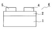
図1に示す半導体発光素子6は、基板1と、この基板1上に形成された第1の窒化物半導体としてAlNからなる下地層2と、この下地層2上に形成された第2の窒化物半導体としてAlGaNからなる発光層3とを含む。そして、発光層3上には第1の電極としてのショットキー電極4と、第2の電極としてのオーミック電極5とが形成されている。
【0013】
本発明において、発光層3は少なくとも一種の希土類元素を含有していることが必要である。希土類元素の含有量については特に限定されるものではなく、希土類元素の種類、発光層2を構成する第2の窒化物半導体の材料組成、及び所望する発光強度などによって任意に選択される。
【0014】
一般的には発光層の結晶性を劣化させない範囲において、できるだけ多くの希土類元素を含有させることが好ましい。具体的には、0.01〜7原子%であることが好ましい。これによって、実用に足る30lm/W程度の発光強度を得ることができる。
【0015】
希土類元素の種類についても特には限定されず、所望する発光波長に応じて任意に選択することができる。例えば、青色領域の波長の光を生成させるためには、Tmを用いることができ、緑色領域の波長の光を生成するためには、Erを用いることができる。さらに、赤色領域の波長の光を生成するためには、Eu又はPrを用いることができる。
【0016】
そして、これらの希土類元素を発光層に添加することにより、各色度領域の波長を有する光が互いに重畳されて、半導体発光素子全体として白色光を生成することができる。希土類元素の添加については、MOCVD法により供給原料として供給することもできるし、イオン注入法などの方法によって成膜後に添加することもできる。
【0017】
本発明者らはさらなる研究の結果、発光層中に希土類元素を添加した際において、前記発光層を構成する半導体のバンドギャップが大きくなるにしたがって、前記希土類元素に起因した発光の効率が増大することを見出した。さらに、本発明のように、発光層がAlを含む窒化物半導体からなる場合においては、この半導体中におけるAl含有量が増大するにつれてバンドギャップが増大する。
【0018】
したがって、発光層を構成する第2の窒化物半導体中におけるAl含有量については50原子%以上であることが好ましく、さらには70原子%以上であることが好ましい。
【0019】
さらに、十分な量の希土類元素を含有し、実用に足る強度の光を安定的に発するようにするためには、発光層2の結晶性が良好であり、下地層との格子定数などの違いに起因する転位が十分に少ない必要がある。したがって、下地層2は、X線ロッキングカーブにおける半値幅が90秒以下、好ましくは50秒以下の高結晶性を有することが必要である。
【0020】
また、下地層2におけるX線ロッキングカーブの半値幅の下限については特に限定されないが、一般的には10秒程度である。
【0021】
このように結晶性の高い下地層を得るには、所定の原料供給ガスを用い、MOCVD法によって好ましくは1100℃以上、さらに好ましくは1150℃以上に加熱することによって形成する。従来の半導体発光素子における下地層の形成温度は500〜700℃であり、この形成温度と比較した場合、上記形成温度が極めて高いことが分かる。すなわち、MOCVD法において従来と全く異なる条件を採用することによって、本発明の条件を満足する結晶性に優れた下地層を形成することができる。
【0022】
また、下地層の形成温度の上限については特に限定されるものではないが、好ましくは1250℃である。これによって、下地層を構成する窒化物半導体の材料組成などに依存した表面の荒れ、さらには下地層内における組成成分の拡散を効果的に抑制することができる。これによって、前記下地層を構成する窒化物半導体の材料組成によらずに、前記下地層の結晶性を良好な状態に保持することが可能となるとともに、表面の荒れに起因する発光層の結晶性の劣化を効果的に防止することができる。
【0023】
また、下地層2を構成する第1の窒化物半導体におけるAl含有量は、50原子%以上であることが好ましく、さらには図1に示すように、AlNから構成することが好ましい。
【0024】
なお、下地層2を構成する第1の窒化物半導体中のAl含有量を上記のように増大させた場合、その格子定数が著しく大きくなるため、下地層2と基板1との間にミスフィットの増大に伴う転位の増加や、下地層2自体の剥離などを生じる場合がある。
【0025】
したがって、基板1と下地層2との間に、基板1側から下地層2側に向けてAl含有量が連続的又はステップ状に増大した緩衝層を設けることが好ましい。これによって、基板1と下地層2との格子定数差を前記緩衝層によって吸収することができ、上記ミスフィット増大に伴う転位の増加や下地層の剥離を効果的に防止することができる。
【0026】
なお、本発明における第2の窒化物半導体は、Al、Ga、及びInの少なくとも一つを含むことが必要であり、そのバンドギャップなどを考慮して任意の組成を有することができる。
【0027】
また、ショットキー電極及びオーミック電極は、InSnの酸化物などから構成され、可視光に対して透明であることが好ましい。
【0028】
また、基板としては、サファイア基板、SiC基板、Si基板、及びGaN基板などを使用することができる。
【0029】
また、図1に示すような本発明の半導体発光素子は、下地層や発光層が上述した要件を満足する限りにおいて、通常の方法にしたがって製造することができる。
【0030】
なお、本発明においては、図1に示すような発光層3を形成することなく、下地層2中に上記希土類元素を含有させることもできる。図2は、このような構成の半導体発光素子の一例を示す断面図である。図2に示すように、このような構成の半導体発光素子においては、ショットキー電極4及びオーミック電極5は、下地層2上に直接的に形成され、下地層2において発光がなされる。したがって、下地層2は発光層としても作用する。
【0031】
【実施例】
2インチ径の厚さ430μmのサファイア基板をH2SO4+H2O2で前処理した後、MOCVD装置の中に設置した。MOCVD装置には、ガス系としてNH3、TMA、TMG、SiH4が取り付けてある。H2を流速10m/secで流しながら、基板を1200℃まで昇温した後、TMAとNH3を平均流速10m/secで流して、下地層としてのAlN層を厚さ1μmまで成長させた。このAlN層のX線回折ロッキングカーブの半値幅は90秒で、良質のAlN層であることがわかった。
【0032】
次いで、成長させたAlN層を保護するために、TMGとNH3をそれぞれ流速10m/secで流して、GaN膜を厚さ100Å成長させた。成長終了後、AlN層とGaN膜のついた基板を取り出し、これをMBE装置の中に設置した。
【0033】
MBE装置の固体源としては、7NのGa、7NのIn、6NのAl、3NのEr、Tm、Euを用いた。窒素源としては、SVTA社の高周波プラズマ装置により発生した原子状窒素を用いた。
【0034】
まず、基板を900℃まで加熱した後、H2とNH3を流すことにより保護層となっていたGaN膜を除去した。その後、基板を100℃まで加熱して30分保持することにより前記AlN層の表面を平坦化し、発光層としてのAl0.9Ga0.1N層を700℃で、厚さ1.0μmに成長させた。この発光層を成長させる際に、Er、Tm、及びEuを0.5原子%の割合でドープさせた。
【0035】
成長終了後、上記のようにして形成したAl0.9Ga0.1N層上に、酸化InSnからなるショットキー接合の透明電極を形成した。
【0036】
その後、前記電極間に電圧20Vを印加したところ、高効率の白色発光を確認した。すなわち、本発明の半導体発光素子が実用的な白色発光素子として動作できることが確かめられた。
【0037】
以上、具体例を挙げながら、本発明を発明の実施の形態に即して詳細に説明してきたが、本発明は上記内容に限定されるものではなく、本発明の範疇を逸脱しない限りにおいてあらゆる変形や変更が可能である。
【0038】
【発明の効果】
以上説明したように、本発明の半導体発光素子によれば、Al、Ga、Inの少なくとも一つを含む窒化物半導体からなる、高結晶性の発光層に希土類元素を添加し、この希土類元素自体を電極間に流した電流によって励起する。そして、この希土類元素に固有の波長の光を素子全体として高効率で生成するようにしている。
【0039】
したがって、希土類元素の種類を適宜に選択することにより、所望の波長を有する光を実用に足る効率で生成することができるとともに、互いに異なる複数の種類の希土類元素を含有させることによって、実用に足る効率で白色光を生成することもできる。
【図面の簡単な説明】
【図1】本発明の半導体発光素子の一例を示す断面図である。
【図2】本発明の半導体発光素子の他の例を示す断面図である。
【符号の説明】
1 基板、2 下地層、3 発光層、4 ショットキー電極、5 オーミック電極、6 半導体発光素子[0001]
BACKGROUND OF THE INVENTION
The present invention relates to a semiconductor light emitting device, and more particularly to a semiconductor light emitting device that can be suitably used as a white light emitting diode.
[0002]
[Prior art]
In recent years, demand for light emitting diodes (LEDs) of various colors has increased. LEDs have low power consumption and long life, so they are not only used for conventional display LEDs, but also increase in demand for lighting from the viewpoint of reducing power consumption and CO2 reduction associated with energy consumption reduction. Is expected.
[0003]
As LEDs, GaAs-based, AlGaAs-based, GaP-based, GaAsP-based, and InGaAlP-based LEDs have been put into practical use, and have been used for various purposes, particularly for display. In recent years, blue and green LEDs have been realized with GaN-based LEDs, so that almost all colors can be arranged with LEDs, and display in all colors has become possible. . In addition, white LEDs using RGB and yellow phosphors are coated on blue LEDs, and white LEDs based on two colors are being put into practical use, and illumination by LEDs is being realized.
[Problems to be solved by the invention]
[0004]
However, since white LEDs using RGB use different LED chips and are expensive, it is considered difficult to put them into practical use for illumination. In addition, since the two-color white LED is not the three primary colors, there is a problem that the full color cannot be recognized under the white light. In addition, the luminance is still only about 251 m / W, and does not reach the 901 m / W of fluorescent lamps.
[0005]
From the above, LEDs with higher efficiency in the three primary colors are craved all over the world for illumination that can solve environmental problems with low energy. In fact, in order to realize such an LED for white illumination, not only a national project in Japan, but also many major electric manufacturers are actively developing in the United States and Europe.
[0006]
An object of this invention is to provide the novel semiconductor light-emitting device which can be used suitably as LED which emits light of arbitrary chromaticity, especially white LED. The “LED” here is a concept including not only a light emitting element using a so-called PN junction but also all semiconductor light emitting elements.
[0007]
[Means for Solving the Problems]
In order to achieve the above object, a semiconductor light emitting device of the present invention includes a substrate and a first nitride semiconductor containing50 atomic percent or less ofAl having a half width of 90 seconds or less in an X-ray rocking curve formed on the substrate. A light emitting layer made of a second nitride semiconductor containing at least one kind of rare earth element as an additive elementand having a composition of AlGaN formed on the light emitting layer, A first electrode composed of a Schottky electrode and a second electrode composed of a Schottky electrode or an ohmic electrode are provided.
[0008]
The present inventors have intensively studied to obtain a white light emitting semiconductor light emitting device. As a result, a substrate, a base layer, and a light emitting layer are provided, and a surface of the light emitting layer includes a first electrode composed of a Schottky electrode and a second electrode composed of a Schottky electrode or an ohmic electrode. In the semiconductor light emitting device in which the light emitting layer is formed of a nitride semiconductor containing at least one of Al, Ga, and In,
While improving the crystallinity of the underlayer and containing a predetermined rare earth element in the light emitting layer and appropriately changing the type of the rare earth element, light having a wavelength unique to the type of the rare earth element is obtained. As a result, the inventors have found that the first semiconductor light-emitting element can be invented.
[0009]
In the semiconductor light emitting device having the above-described configuration, since the light emitting layer contains a rare earth element, the rare earth element is excited by electrons injected from the electrode, and emits light having a wavelength specific to the type of the rare earth element. It is something that is emitted.
[0010]
And the light emission wavelength from the said semiconductor light emitting element can be arbitrarily controlled by adjusting the kind of this rare earth element suitably. Further, by appropriately including a plurality of types of rare earth elements, emission wavelengths from these rare earth elements are superimposed, and white light can be generated as a whole semiconductor light emitting element.
[0011]
Further, in the semiconductor light emitting device described above, the role as a light emitting layer can be superimposed on this underlayer by adding a rare earth element directly to the underlayer. In this case, the light emitting layer as described above is not necessary.
[0012]
DETAILED DESCRIPTION OF THE INVENTION
Hereinafter, the present invention will be described in detail according to embodiments of the invention.
FIG. 1 is a cross-sectional view showing an example of a semiconductor light emitting device of the present invention.
A semiconductor
[0013]
In the present invention, the
[0014]
In general, it is preferable to contain as much rare earth element as possible within a range not deteriorating the crystallinity of the light emitting layer. Specifically, it is preferably 0.01 to 7 atomic%. As a result, a light emission intensity of about 30 lm / W, which is practical, can be obtained.
[0015]
The type of rare earth element is not particularly limited, and can be arbitrarily selected according to a desired emission wavelength. For example, Tm can be used to generate light with a wavelength in the blue region, and Er can be used to generate light with a wavelength in the green region. Further, Eu or Pr can be used to generate light having a wavelength in the red region.
[0016]
Then, by adding these rare earth elements to the light emitting layer, light having wavelengths in each chromaticity region is superimposed on each other, and white light can be generated as the entire semiconductor light emitting element. The rare earth element can be added as a raw material by MOCVD, or can be added after film formation by a method such as ion implantation.
[0017]
As a result of further studies, the inventors have found that when a rare earth element is added to the light emitting layer, the efficiency of light emission caused by the rare earth element increases as the band gap of the semiconductor constituting the light emitting layer increases. I found out. Further, when the light emitting layer is made of a nitride semiconductor containing Al as in the present invention, the band gap increases as the Al content in the semiconductor increases.
[0018]
Therefore, the Al content in the second nitride semiconductor constituting the light emitting layer is preferably 50 atomic% or more, and more preferably 70 atomic% or more.
[0019]
Further, in order to stably emit light having a sufficient amount of rare earth elements and having a practical intensity, the crystallinity of the
[0020]
Further, the lower limit of the full width at half maximum of the X-ray rocking curve in the
[0021]
In order to obtain an underlayer with high crystallinity as described above, it is formed by using a predetermined raw material supply gas and preferably heating to 1100 ° C. or higher, more preferably 1150 ° C. or higher by MOCVD. The formation temperature of the underlayer in the conventional semiconductor light emitting device is 500 to 700 ° C., and it can be seen that the formation temperature is extremely high when compared with this formation temperature. That is, by adopting completely different conditions in the MOCVD method, it is possible to form an underlayer with excellent crystallinity that satisfies the conditions of the present invention.
[0022]
The upper limit of the formation temperature of the underlayer is not particularly limited, but is preferably 1250 ° C. As a result, it is possible to effectively suppress surface roughness depending on the material composition of the nitride semiconductor constituting the underlayer, and further, diffusion of composition components in the underlayer. This makes it possible to maintain the crystallinity of the underlayer in a good state regardless of the material composition of the nitride semiconductor that constitutes the underlayer, and the crystal of the light-emitting layer due to surface roughness. Deterioration can be effectively prevented.
[0023]
Further, the Al content in the first nitride semiconductor constituting the
[0024]
Note that, when the Al content in the first nitride semiconductor constituting the
[0025]
Therefore, it is preferable to provide a buffer layer in which the Al content increases continuously or stepwise from the
[0026]
Note that the second nitride semiconductor in the present invention needs to contain at least one of Al, Ga, and In, and can have any composition in consideration of the band gap and the like.
[0027]
In addition, the Schottky electrode and the ohmic electrode are preferably made of an oxide of InSn or the like and are transparent to visible light.
[0028]
As the substrate, a sapphire substrate, a SiC substrate, a Si substrate, a GaN substrate, or the like can be used.
[0029]
Further, the semiconductor light emitting device of the present invention as shown in FIG. 1 can be manufactured according to a usual method as long as the underlayer and the light emitting layer satisfy the above-described requirements.
[0030]
In the present invention, the rare earth element can be contained in the
[0031]
【Example】
A sapphire substrate having a 2 inch diameter and a thickness of 430 μm was pretreated with H2 SO4 + H2 O2 and then placed in an MOCVD apparatus. In the MOCVD apparatus, NH3 , TMA, TMG, and SiH4 are attached as gas systems. The substrate was heated to 1200 ° C. while flowing H2 at a flow rate of 10 m / sec, and then TMA and NH3 were flowed at an average flow rate of 10 m / sec to grow an AlN layer as a base layer to a thickness of 1 μm. The half width of the X-ray diffraction rocking curve of this AlN layer was 90 seconds, and it was found that the AlN layer was a good quality AlN layer.
[0032]
Next, in order to protect the grown AlN layer, TMG and NH3 were flowed at a flow rate of 10 m / sec to grow a GaN film with a thickness of 100 mm. After the growth was completed, the substrate with the AlN layer and the GaN film was taken out and placed in an MBE apparatus.
[0033]
As solid sources of the MBE apparatus, 7N Ga, 7N In, 6N Al, 3N Er, Tm, and Eu were used. As the nitrogen source, atomic nitrogen generated by a high-frequency plasma apparatus manufactured by SVTA was used.
[0034]
First, after heating the substrate to 900 ° C., the GaN film serving as the protective layer was removed by flowing H2 and NH3 . Thereafter, the substrate is heated to 100 ° C. and held for 30 minutes to flatten the surface of the AlN layer, and an Al0.9 Ga0.1 N layer as a light emitting layer is formed at 700 ° C. to a thickness of 1.0 μm. Grown up. In growing this light emitting layer, Er, Tm, and Eu were doped at a ratio of 0.5 atomic%.
[0035]
After completion of the growth, a Schottky junction transparent electrode made of oxidized InSn was formed on the Al0.9 Ga0.1 N layer formed as described above.
[0036]
Thereafter, when a voltage of 20 V was applied between the electrodes, high-efficiency white light emission was confirmed. That is, it was confirmed that the semiconductor light emitting device of the present invention can operate as a practical white light emitting device.
[0037]
As mentioned above, the present invention has been described in detail according to the embodiments of the present invention with specific examples. However, the present invention is not limited to the above-described contents, and is not limited to the scope of the present invention. Variations and changes are possible.
[0038]
【The invention's effect】
As described above, according to the semiconductor light emitting device of the present invention, a rare earth element is added to a highly crystalline light emitting layer made of a nitride semiconductor containing at least one of Al, Ga, and In, and the rare earth element itself. Is excited by a current flowing between the electrodes. And the light of the wavelength peculiar to this rare earth element is generated with high efficiency as the whole element.
[0039]
Therefore, by appropriately selecting the type of rare earth element, light having a desired wavelength can be generated with practical efficiency, and by including a plurality of different types of rare earth elements, it is sufficient for practical use. White light can also be generated efficiently.
[Brief description of the drawings]
FIG. 1 is a cross-sectional view showing an example of a semiconductor light emitting device of the present invention.
FIG. 2 is a cross-sectional view showing another example of the semiconductor light emitting device of the present invention.
[Explanation of symbols]
DESCRIPTION OF
Claims (6)
Translated fromJapanesePriority Applications (2)
| Application Number | Priority Date | Filing Date | Title |
|---|---|---|---|
| JP2001001149AJP3819713B2 (en) | 2001-01-09 | 2001-01-09 | Semiconductor light emitting device |
| US10/035,001US6693302B2 (en) | 2001-01-09 | 2001-12-28 | Semiconductor light-emitting element |
Applications Claiming Priority (1)
| Application Number | Priority Date | Filing Date | Title |
|---|---|---|---|
| JP2001001149AJP3819713B2 (en) | 2001-01-09 | 2001-01-09 | Semiconductor light emitting device |
Publications (2)
| Publication Number | Publication Date |
|---|---|
| JP2002208731A JP2002208731A (en) | 2002-07-26 |
| JP3819713B2true JP3819713B2 (en) | 2006-09-13 |
Family
ID=18869818
Family Applications (1)
| Application Number | Title | Priority Date | Filing Date |
|---|---|---|---|
| JP2001001149AExpired - LifetimeJP3819713B2 (en) | 2001-01-09 | 2001-01-09 | Semiconductor light emitting device |
Country Status (2)
| Country | Link |
|---|---|
| US (1) | US6693302B2 (en) |
| JP (1) | JP3819713B2 (en) |
Families Citing this family (7)
| Publication number | Priority date | Publication date | Assignee | Title |
|---|---|---|---|---|
| JP4327339B2 (en)* | 2000-07-28 | 2009-09-09 | 独立行政法人物質・材料研究機構 | Semiconductor layer forming substrate and semiconductor device using the same |
| JP3720341B2 (en)* | 2003-02-12 | 2005-11-24 | ローム株式会社 | Semiconductor light emitting device |
| JP2011082528A (en)* | 2003-11-26 | 2011-04-21 | Ricoh Co Ltd | Semiconductor light-emitting device |
| JP2005203418A (en)* | 2004-01-13 | 2005-07-28 | Hitachi Cable Ltd | Nitride-based compound semiconductor substrate and method for manufacturing the same |
| KR101039982B1 (en) | 2010-03-18 | 2011-06-09 | 엘지이노텍 주식회사 | Light emitting device and manufacturing method |
| KR101039937B1 (en)* | 2010-04-28 | 2011-06-09 | 엘지이노텍 주식회사 | Light emitting device, manufacturing method of light emitting device, light emitting device package and lighting system |
| KR101605262B1 (en)* | 2014-10-16 | 2016-04-04 | 한양대학교 산학협력단 | Light emitting device and method of fabricating the same |
Family Cites Families (6)
| Publication number | Priority date | Publication date | Assignee | Title |
|---|---|---|---|---|
| JP3360945B2 (en)* | 1994-07-15 | 2003-01-07 | シャープ株式会社 | Electrode structure and manufacturing method thereof |
| TW383508B (en)* | 1996-07-29 | 2000-03-01 | Nichia Kagaku Kogyo Kk | Light emitting device and display |
| JP3813740B2 (en)* | 1997-07-11 | 2006-08-23 | Tdk株式会社 | Substrates for electronic devices |
| JP3822318B2 (en)* | 1997-07-17 | 2006-09-20 | 株式会社東芝 | Semiconductor light emitting device and manufacturing method thereof |
| US6104074A (en)* | 1997-12-11 | 2000-08-15 | Apa Optics, Inc. | Schottky barrier detectors for visible-blind ultraviolet detection |
| US6140669A (en)* | 1999-02-20 | 2000-10-31 | Ohio University | Gallium nitride doped with rare earth ions and method and structure for achieving visible light emission |
- 2001
- 2001-01-09JPJP2001001149Apatent/JP3819713B2/ennot_activeExpired - Lifetime
- 2001-12-28USUS10/035,001patent/US6693302B2/ennot_activeExpired - Lifetime
Also Published As
| Publication number | Publication date |
|---|---|
| US20020149028A1 (en) | 2002-10-17 |
| US6693302B2 (en) | 2004-02-17 |
| JP2002208731A (en) | 2002-07-26 |
Similar Documents
| Publication | Publication Date | Title |
|---|---|---|
| KR102569461B1 (en) | Light emitting device and lighting apparatus including the same | |
| JP4063520B2 (en) | Semiconductor light emitting device | |
| USRE40485E1 (en) | Semiconductor light-emitting element | |
| US7884351B2 (en) | Nitride semiconductor light-emitting device | |
| JPH11135838A (en) | White light emitting diode and method of manufacturing the same | |
| CN101728472A (en) | Multilayer LED chip structure and preparation method thereof | |
| US12125945B2 (en) | Single chip multi band LED | |
| JP2015177025A (en) | optical semiconductor element | |
| AU2005322570A1 (en) | High efficiency light-emitting diodes | |
| JP3888668B2 (en) | Semiconductor light emitting device | |
| JP3978858B2 (en) | Gallium nitride compound semiconductor light emitting device | |
| Nakamura | High-power InGaN/AlGaN double-heterostructure blue-light-emitting diodes | |
| JP3819713B2 (en) | Semiconductor light emitting device | |
| JP5896454B2 (en) | Red light emitting semiconductor device and method for manufacturing the same | |
| JP2000196142A (en) | Light emitting element | |
| Nakamura | InGaN light-emitting diodes with quantum-well structures | |
| JP2004288757A (en) | Semiconductor light emitting element | |
| JP2005228802A (en) | Fluorescence emitting device, fluorescence emitting element and fluorescence substance | |
| US20120313125A1 (en) | Light emitting devices with efficient wavelength conversion and associated methods | |
| Nakamura et al. | InGaN single-quantum-well LEDs | |
| JP2003197969A (en) | GaN-based semiconductor light-emitting element and light-emitting device using the same | |
| KR20120002818A (en) | Nitride semiconductor light emitting device and manufacturing method | |
| JP2005259864A (en) | Method for emitting multicolored light | |
| JP4351600B2 (en) | Semiconductor light emitting device | |
| KR101562928B1 (en) | Light Emitting Diode and manufacturing method of the same |
Legal Events
| Date | Code | Title | Description |
|---|---|---|---|
| A977 | Report on retrieval | Free format text:JAPANESE INTERMEDIATE CODE: A971007 Effective date:20040105 | |
| A131 | Notification of reasons for refusal | Free format text:JAPANESE INTERMEDIATE CODE: A131 Effective date:20040113 | |
| A521 | Request for written amendment filed | Free format text:JAPANESE INTERMEDIATE CODE: A523 Effective date:20040308 | |
| A02 | Decision of refusal | Free format text:JAPANESE INTERMEDIATE CODE: A02 Effective date:20041207 | |
| A521 | Request for written amendment filed | Free format text:JAPANESE INTERMEDIATE CODE: A523 Effective date:20060418 | |
| RD04 | Notification of resignation of power of attorney | Free format text:JAPANESE INTERMEDIATE CODE: A7424 Effective date:20060420 | |
| A61 | First payment of annual fees (during grant procedure) | Free format text:JAPANESE INTERMEDIATE CODE: A61 Effective date:20060615 | |
| R150 | Certificate of patent or registration of utility model | Free format text:JAPANESE INTERMEDIATE CODE: R150 Ref document number:3819713 Country of ref document:JP Free format text:JAPANESE INTERMEDIATE CODE: R150 | |
| S201 | Request for registration of exclusive licence | Free format text:JAPANESE INTERMEDIATE CODE: R314201 | |
| FPAY | Renewal fee payment (event date is renewal date of database) | Free format text:PAYMENT UNTIL: 20090623 Year of fee payment:3 | |
| R350 | Written notification of registration of transfer | Free format text:JAPANESE INTERMEDIATE CODE: R350 | |
| FPAY | Renewal fee payment (event date is renewal date of database) | Free format text:PAYMENT UNTIL: 20100623 Year of fee payment:4 | |
| FPAY | Renewal fee payment (event date is renewal date of database) | Free format text:PAYMENT UNTIL: 20100623 Year of fee payment:4 | |
| FPAY | Renewal fee payment (event date is renewal date of database) | Free format text:PAYMENT UNTIL: 20110623 Year of fee payment:5 | |
| FPAY | Renewal fee payment (event date is renewal date of database) | Free format text:PAYMENT UNTIL: 20120623 Year of fee payment:6 | |
| FPAY | Renewal fee payment (event date is renewal date of database) | Free format text:PAYMENT UNTIL: 20130623 Year of fee payment:7 | |
| FPAY | Renewal fee payment (event date is renewal date of database) | Free format text:PAYMENT UNTIL: 20140623 Year of fee payment:8 | |
| EXPY | Cancellation because of completion of term |