JP3819660B2 - Semiconductor device manufacturing method and semiconductor manufacturing apparatus - Google Patents
Semiconductor device manufacturing method and semiconductor manufacturing apparatusDownload PDFInfo
- Publication number
- JP3819660B2 JP3819660B2JP2000037120AJP2000037120AJP3819660B2JP 3819660 B2JP3819660 B2JP 3819660B2JP 2000037120 AJP2000037120 AJP 2000037120AJP 2000037120 AJP2000037120 AJP 2000037120AJP 3819660 B2JP3819660 B2JP 3819660B2
- Authority
- JP
- Japan
- Prior art keywords
- reaction tube
- substrate
- film
- distance
- quartz
- Prior art date
- Legal status (The legal status is an assumption and is not a legal conclusion. Google has not performed a legal analysis and makes no representation as to the accuracy of the status listed.)
- Expired - Lifetime
Links
Images


Classifications
- C—CHEMISTRY; METALLURGY
- C23—COATING METALLIC MATERIAL; COATING MATERIAL WITH METALLIC MATERIAL; CHEMICAL SURFACE TREATMENT; DIFFUSION TREATMENT OF METALLIC MATERIAL; COATING BY VACUUM EVAPORATION, BY SPUTTERING, BY ION IMPLANTATION OR BY CHEMICAL VAPOUR DEPOSITION, IN GENERAL; INHIBITING CORROSION OF METALLIC MATERIAL OR INCRUSTATION IN GENERAL
- C23C—COATING METALLIC MATERIAL; COATING MATERIAL WITH METALLIC MATERIAL; SURFACE TREATMENT OF METALLIC MATERIAL BY DIFFUSION INTO THE SURFACE, BY CHEMICAL CONVERSION OR SUBSTITUTION; COATING BY VACUUM EVAPORATION, BY SPUTTERING, BY ION IMPLANTATION OR BY CHEMICAL VAPOUR DEPOSITION, IN GENERAL
- C23C16/00—Chemical coating by decomposition of gaseous compounds, without leaving reaction products of surface material in the coating, i.e. chemical vapour deposition [CVD] processes
- C23C16/22—Chemical coating by decomposition of gaseous compounds, without leaving reaction products of surface material in the coating, i.e. chemical vapour deposition [CVD] processes characterised by the deposition of inorganic material, other than metallic material
- C23C16/30—Deposition of compounds, mixtures or solid solutions, e.g. borides, carbides, nitrides
- C23C16/34—Nitrides
- C23C16/345—Silicon nitride
- H—ELECTRICITY
- H01—ELECTRIC ELEMENTS
- H01L—SEMICONDUCTOR DEVICES NOT COVERED BY CLASS H10
- H01L21/00—Processes or apparatus adapted for the manufacture or treatment of semiconductor or solid state devices or of parts thereof
- H01L21/02—Manufacture or treatment of semiconductor devices or of parts thereof
- H01L21/02104—Forming layers
- H01L21/02107—Forming insulating materials on a substrate
- H01L21/02225—Forming insulating materials on a substrate characterised by the process for the formation of the insulating layer
- H01L21/0226—Forming insulating materials on a substrate characterised by the process for the formation of the insulating layer formation by a deposition process
- H01L21/02263—Forming insulating materials on a substrate characterised by the process for the formation of the insulating layer formation by a deposition process deposition from the gas or vapour phase
- H01L21/02271—Forming insulating materials on a substrate characterised by the process for the formation of the insulating layer formation by a deposition process deposition from the gas or vapour phase deposition by decomposition or reaction of gaseous or vapour phase compounds, i.e. chemical vapour deposition
- C—CHEMISTRY; METALLURGY
- C23—COATING METALLIC MATERIAL; COATING MATERIAL WITH METALLIC MATERIAL; CHEMICAL SURFACE TREATMENT; DIFFUSION TREATMENT OF METALLIC MATERIAL; COATING BY VACUUM EVAPORATION, BY SPUTTERING, BY ION IMPLANTATION OR BY CHEMICAL VAPOUR DEPOSITION, IN GENERAL; INHIBITING CORROSION OF METALLIC MATERIAL OR INCRUSTATION IN GENERAL
- C23C—COATING METALLIC MATERIAL; COATING MATERIAL WITH METALLIC MATERIAL; SURFACE TREATMENT OF METALLIC MATERIAL BY DIFFUSION INTO THE SURFACE, BY CHEMICAL CONVERSION OR SUBSTITUTION; COATING BY VACUUM EVAPORATION, BY SPUTTERING, BY ION IMPLANTATION OR BY CHEMICAL VAPOUR DEPOSITION, IN GENERAL
- C23C16/00—Chemical coating by decomposition of gaseous compounds, without leaving reaction products of surface material in the coating, i.e. chemical vapour deposition [CVD] processes
- C23C16/44—Chemical coating by decomposition of gaseous compounds, without leaving reaction products of surface material in the coating, i.e. chemical vapour deposition [CVD] processes characterised by the method of coating
- C23C16/458—Chemical coating by decomposition of gaseous compounds, without leaving reaction products of surface material in the coating, i.e. chemical vapour deposition [CVD] processes characterised by the method of coating characterised by the method used for supporting substrates in the reaction chamber
- C23C16/4582—Rigid and flat substrates, e.g. plates or discs
- C23C16/4583—Rigid and flat substrates, e.g. plates or discs the substrate being supported substantially horizontally
- H—ELECTRICITY
- H01—ELECTRIC ELEMENTS
- H01L—SEMICONDUCTOR DEVICES NOT COVERED BY CLASS H10
- H01L21/00—Processes or apparatus adapted for the manufacture or treatment of semiconductor or solid state devices or of parts thereof
- H01L21/02—Manufacture or treatment of semiconductor devices or of parts thereof
- H01L21/02104—Forming layers
- H01L21/02107—Forming insulating materials on a substrate
- H01L21/02109—Forming insulating materials on a substrate characterised by the type of layer, e.g. type of material, porous/non-porous, pre-cursors, mixtures or laminates
- H01L21/02112—Forming insulating materials on a substrate characterised by the type of layer, e.g. type of material, porous/non-porous, pre-cursors, mixtures or laminates characterised by the material of the layer
- H01L21/02123—Forming insulating materials on a substrate characterised by the type of layer, e.g. type of material, porous/non-porous, pre-cursors, mixtures or laminates characterised by the material of the layer the material containing silicon
- H01L21/02126—Forming insulating materials on a substrate characterised by the type of layer, e.g. type of material, porous/non-porous, pre-cursors, mixtures or laminates characterised by the material of the layer the material containing silicon the material containing Si, O, and at least one of H, N, C, F, or other non-metal elements, e.g. SiOC, SiOC:H or SiONC
- H01L21/0214—Forming insulating materials on a substrate characterised by the type of layer, e.g. type of material, porous/non-porous, pre-cursors, mixtures or laminates characterised by the material of the layer the material containing silicon the material containing Si, O, and at least one of H, N, C, F, or other non-metal elements, e.g. SiOC, SiOC:H or SiONC the material being a silicon oxynitride, e.g. SiON or SiON:H
- H—ELECTRICITY
- H01—ELECTRIC ELEMENTS
- H01L—SEMICONDUCTOR DEVICES NOT COVERED BY CLASS H10
- H01L21/00—Processes or apparatus adapted for the manufacture or treatment of semiconductor or solid state devices or of parts thereof
- H01L21/02—Manufacture or treatment of semiconductor devices or of parts thereof
- H01L21/02104—Forming layers
- H01L21/02107—Forming insulating materials on a substrate
- H01L21/02109—Forming insulating materials on a substrate characterised by the type of layer, e.g. type of material, porous/non-porous, pre-cursors, mixtures or laminates
- H01L21/02205—Forming insulating materials on a substrate characterised by the type of layer, e.g. type of material, porous/non-porous, pre-cursors, mixtures or laminates the layer being characterised by the precursor material for deposition
- H01L21/02208—Forming insulating materials on a substrate characterised by the type of layer, e.g. type of material, porous/non-porous, pre-cursors, mixtures or laminates the layer being characterised by the precursor material for deposition the precursor containing a compound comprising Si
- H01L21/02219—Forming insulating materials on a substrate characterised by the type of layer, e.g. type of material, porous/non-porous, pre-cursors, mixtures or laminates the layer being characterised by the precursor material for deposition the precursor containing a compound comprising Si the compound comprising silicon and nitrogen
- H—ELECTRICITY
- H01—ELECTRIC ELEMENTS
- H01L—SEMICONDUCTOR DEVICES NOT COVERED BY CLASS H10
- H01L21/00—Processes or apparatus adapted for the manufacture or treatment of semiconductor or solid state devices or of parts thereof
- H01L21/02—Manufacture or treatment of semiconductor devices or of parts thereof
- H01L21/02104—Forming layers
- H01L21/02107—Forming insulating materials on a substrate
- H01L21/02109—Forming insulating materials on a substrate characterised by the type of layer, e.g. type of material, porous/non-porous, pre-cursors, mixtures or laminates
- H01L21/02112—Forming insulating materials on a substrate characterised by the type of layer, e.g. type of material, porous/non-porous, pre-cursors, mixtures or laminates characterised by the material of the layer
- H01L21/02123—Forming insulating materials on a substrate characterised by the type of layer, e.g. type of material, porous/non-porous, pre-cursors, mixtures or laminates characterised by the material of the layer the material containing silicon
- H01L21/0217—Forming insulating materials on a substrate characterised by the type of layer, e.g. type of material, porous/non-porous, pre-cursors, mixtures or laminates characterised by the material of the layer the material containing silicon the material being a silicon nitride not containing oxygen, e.g. SixNy or SixByNz
Landscapes
- Chemical & Material Sciences (AREA)
- Engineering & Computer Science (AREA)
- Manufacturing & Machinery (AREA)
- General Physics & Mathematics (AREA)
- Physics & Mathematics (AREA)
- Computer Hardware Design (AREA)
- Microelectronics & Electronic Packaging (AREA)
- Power Engineering (AREA)
- Condensed Matter Physics & Semiconductors (AREA)
- Chemical Kinetics & Catalysis (AREA)
- General Chemical & Material Sciences (AREA)
- Materials Engineering (AREA)
- Mechanical Engineering (AREA)
- Metallurgy (AREA)
- Organic Chemistry (AREA)
- Inorganic Chemistry (AREA)
- Chemical Vapour Deposition (AREA)
- Formation Of Insulating Films (AREA)
Description
Translated fromJapanese【0001】
【発明の属する技術分野】
本発明は、半導体装置の製造方法および半導体製造装置に関し、特に、半導体装置に使用される窒化シリコン膜および酸化窒化シリコン膜の熱CVD(Chemical Vapor Deposition)法による成膜工程を有する半導体装置の製造方法および当該方法に好適に使用される半導体製造装置に関する。
【0002】
【従来の技術】
従来、半導体装置に使用される窒化シリコン膜は、SiH2Cl2(以下DCSと記す)とNH3との混合ガスにより形成するのが一般的である。また、半導体装置に使用される酸化窒化シリコン膜は、DCSとNH3とN2Oとの混合ガスにより形成するのが一般的である。
【0003】
しかしながら、この方法では、700℃〜800℃といった高温で窒化シリコン膜や酸化窒化シリコン膜を形成する必要があり、その結果、浅い拡散層内の不純物が熱により深く拡散してしまい、素子寸法を小さくできないという問題がある。また、排気口に反応副生成物であるNH4Cl(塩化アンモニウム)が付着してしまい、このNH4Clは金属表面に錆を生じさせ、半導体ウェーハ上に金属汚染を生じさせるという問題もある。
【0004】
【発明が解決しようとする課題】
これらの問題点を解決するために、本発明者らは、SiH2(NH(C4H9))2(ビス ターシャル ブチル アミノ シラン:BTBAS:Bis tertial butyl amino silane)とNH3とを原料ガスとして用いて窒化シリコン(Si3N4)膜を形成することや、BTBASとNH3とN2Oとを原料ガスとして用いて酸化窒化シリコン膜を形成することを検討した。その結果、このようにすれば、600℃程度の低温で窒化シリコン膜や酸化窒化シリコン膜を成膜可能であり、また、金属汚染の原因であるNH4Clを発生させないことが判明した。
【0005】
しかしながら、本発明者らは、BTBASを用いて窒化シリコン膜や酸化窒化シリコン膜を成膜する場合には成膜された膜の面内均一性が充分でないことを見いだした。
【0006】
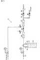
BTBASとNH3とを原料ガスとして用いて窒化シリコン膜を成膜する際や、BTBASとNH3とN2Oとを原料ガスとして用いて酸化窒化シリコン膜を形成する際に使用される炉構成を図1に示す。
【0007】
BTBASとNH3とを原料ガスとして用いて窒化シリコン膜を成膜する場合を例にとって説明する。
【0008】
外側に石英反応管(アウターチューブ)11があり、その内側に筒状の石英インナーチューブ12が入っている。さらに石英インナーチューブ12の内側には石英ボート14が入っており石英ボート14は多数の半導体ウェーハ16を支持している。
【0009】
BTBASとNH3は石英ノズル21、18をそれぞれを通して炉内へ導入される。ガスはまず石英インナーチューブ12内に導入され下から上へ流れる。そして石英インナーチューブ12の外側へ上から下へ排気されていく。
【0010】
この過程で熱分解したBTBASとNH3は、半導体ウェーハ16や石英表面上にSi3N4を形成する。
【0011】
ここで、石英インナーチューブ12とその内部の概略横断面図を図4Aに、概略縦断面図を図4Bにそれぞれ示す。
【0012】
本発明者らは、まず、他の原料ガス系で使用されている構成のものを用いて、BTBASとNH3とを原料ガスとして用いて窒化シリコン膜を成膜した。
【0013】
直径200mmの半導体ウェーハ16を内径260mmの石英インナーチューブ12内に垂直方向にボート柱25によって複数枚積層して成膜した。半導体ウェーハ16の端部(エッジ)と石英インナーチューブ12の内壁との距離bは30mmである。隣接する半導体ウェーハ間の距離aは6.35mmであった。
【0014】
その結果、ウェーハの周辺部でSi3N4膜が厚くなり、中心部が薄いすりばち状になってしまった。BTBASとNH3とN2Oとを原料ガスとして用いて酸化窒化シリコン膜を形成した場合も同様であった。
【0015】
従って、本発明の主な目的は、BTBASとNH3とを原料ガスとして用いて窒化シリコン膜を成膜する際や、BTBASとNH3とN2Oとを原料ガスとして用いて酸化窒化シリコン膜を形成する際に、成膜される膜の膜厚の基板面内均一性を向上することができる成膜方法および成膜装置を提供することにある。
【0016】
【課題を解決するための手段】
本発明者らは、上記課題を解決するために、半導体ウェーハ16の中心部では、その上下に他の半導体ウェーハ16が位置しているために半導体ウェーハ近傍の空間が小さいのに対して、半導体ウェーハ周辺部では石英インナーチューブ12との間に大きい空間が存在するために、上記のようにウェーハの周辺部で厚く、中心部で薄いすりばち状になってしまったのではないかと考えて、半導体ウェーハ16間の距離aと半導体ウェーハ16の端部と石英インナーチューブ12の内壁との間の距離bとの関係と、膜圧の面内分布との関係を鋭意研究の結果、本発明に到達した。
【0017】
すなわち、本発明によれば、
複数の基板を積層して収容する反応管内に、ビス ターシャル ブチル アミノ シランとNH3とを原料ガスとして前記反応管内に流して熱CVD法により前記基板上に窒化シリコン膜を成膜する工程を有する半導体装置の製造方法であって、
前記基板の端部と前記反応管内壁との間の距離bと隣接する前記基板間の距離aとの比b/aの値を0.96以上1.1以下として前記基板上に前記窒化シリコン膜を成膜することを特徴とする半導体装置の製造方法が提供される。
【0019】
また、本発明によれば、
複数の基板を積層して収容する反応管内に、ビス ターシャル ブチル アミノ シランとNH3とN2Oとを原料ガスとして前記反応管内に流して熱CVD法により前記基板上に酸化窒化シリコン膜を成膜する工程を有する半導体装置の製造方法であって、
前記基板の端部と前記反応管内壁との間の距離bと隣接する前記基板間の距離aとの比b/aの値を0.96以上1.1以下として前記基板上に前記酸化窒化シリコン膜を成膜することを特徴とする半導体装置の製造方法が提供される。
【0021】
また、本発明によれば、前記基板が半導体ウェーハであり、前記上記各成膜方法により前記半導体ウェーハ上に成膜する工程を備えることを特徴とする半導体装置の製造方法が提供される。
【0022】
また、本発明によれば、
反応管と、
前記反応管内において複数の基板を積層して保持可能な基板保持手段と、
前記反応管内に、ビス ターシャル ブチル アミノ シランとNH3とを原料ガスとして前記反応管内に流して供給するガス供給手段と、
加熱手段とを備え、
前記基板の端部と前記反応管内壁との間の距離bと隣接する前記基板間の距離aとの比b/aの値を0.96以上1.1以下として前記基板上に熱CVD法により窒化シリコン膜を成膜することを特徴とする半導体製造装置が提供される。
【0024】
また、本発明によれば、
反応管と、
前記反応管内において複数の基板を積層して保持可能な基板保持手段と、
前記反応管内に、ビス ターシャル ブチル アミノ シランとNH3とN2Oとを原料ガスとして前記反応管内に流して供給するガス供給手段と、
加熱手段とを備え、
前記基板の端部と前記反応管内壁との間の距離bと隣接する前記基板間の距離aとの比b/aの値を0.96以上1.1以下として前記基板上に熱CVD法により酸化窒化シリコン膜を成膜することを特徴とする半導体製造装置が提供される。
【0026】
【発明の実施の形態】
次に、図面を参照して本発明の一実施の形態を説明する。
【0027】
本発明において使用するBTBASは常温では液体であるので、図2、図3に示すようなBTBAS供給装置を用いて炉内へ導入する。
【0028】
図2に示すBTBAS供給装置は、恒温槽と気体流量制御の組合せである。図3に示すBTBAS供給装置は、液体流量制御と気化器との組合せにより流量制御を行うものである。
【0029】
図2を参照すれば、BTBAS供給装置4においては、BTBAS液体原料42を備えた恒温槽41内を加熱することによって気化したBTBASの蒸気圧を高める。気化したBTBASは、マスフローコントローラ43により流量制御されて、BTBAS供給口44より図1に示す縦型LPCVD(減圧CVD)成膜装置のノズル21の供給口22に供給される。
【0030】
なお、このBTBAS供給装置4においては、BTBAS液体原料42からBTBAS供給口44に至るまでの配管は、配管加熱部材45によって覆われている。
【0031】
図3を参照すれば、BTBAS供給装置5においては、BTBAS液体原料52を備えたBTBASタンク51内に、押し出しガス導入口53から導入された押し出しガスHeまたはN2を配管54を介して導入することにより、BTBAS液体原料52を配管55に押し出し、その後BTBAS液体原料は、液体流量制御装置56により流量制御されて気化器57に送られ、気化器57で気化されてBTBAS供給口58より図1に示す縦型LPCVD(減圧CVD)成膜装置のノズル21の供給口22に供給される。なお、このBTBAS供給装置5においては、気化器57からBTBAS供給口58に至るまでの配管は、配管加熱部材59によって覆われている。
【0032】
次に、本実施の形態で好適に使用できる縦型LPCVD成膜装置を図1を参照して説明する。
【0033】
縦型LPCVD成膜装置1においては、石英反応管11の外部にヒータ13を備えており、石英反応管11内を均一に加熱できる構造となっている。石英反応管11内には筒状の石英インナーチューブ12が設けられている。石英インナーチューブ12内には、複数の半導体ウェーハを垂直方向に積層して搭載する石英ボート14が設けられている。この石英ボート14は、キャップ15上に搭載されており、キャップ15を上下させることにより、石英インナーチューブ12内に挿入され、また石英インナーチューブ12から取り出される。石英反応管11および石英インナーチューブ12の下部は開放された構造となっているが、キャップ15を上昇させることにより、キャップ15の底板24により閉じられ気密な構造となる。石英インナーチューブ12の下部には、石英ノズル18、21が連通して設けられている。石英インナーチューブ12の上部は開放されている。石英インナーチューブ12と石英反応管11との間の空間の下部には、排気口17が連通して設けられている。排気口17は真空ポンプ(図示せず)に連通しており、石英反応管11内を減圧できる。石英ノズル18、21から供給された原料ガスは、各々の噴出口20、23から石英インナーチューブ12内に噴出され、その後、石英インナーチューブ12内を下部から上部まで移動し、石英インナーチューブ12と石英反応管11との間の空間を通って下方に流れ、排気口17から排気される。
【0034】
次に、この縦型LPCVD成膜装置1を使用して窒化シリコン膜を製造する方法について説明する。
【0035】
まず、多数枚の半導体ウェーハ16を保持した石英ボート14を600℃以下の温度に保たれた石英インナーチューブ12内に挿入する。
【0036】
次に、真空ポンプ(図示せず)を用いて排気口17より真空排気する。ウェーハの面内温度安定効果を得るため、1時間程度排気することが好ましい。
【0037】
次に、石英ノズル18の注入口19よりNH3ガスを注入し、石英反応管11内を、BTBASを流す前にNH3でパージする。
【0038】
次に、石英ノズル18の注入口19よりNH3ガスを注入し続けると共に、石英ノズル21の注入口22よりBTBASを注入して、半導体ウェーハ16上にSi3N4膜を成膜する。
【0039】
次に、石英ノズル18の注入口19よりNH3ガスを注入したまま、BTBASの供給を停止して、石英反応管11内をNH3でパージする。
【0040】
BTBASのみ流すとSi3N4膜とは異なる膜ができるため、デポジション前後にNH3によるパージを行うことが好ましい。
【0041】
次に、石英ノズル18よりN2を石英反応管11内に流入させてN2パージを行い、石英反応管11内のNH3を除去する。
【0042】
その後、N2の供給を止めて石英反応管11内を真空にする。N2パージとその後の石英反応管11内の真空排気は数回セットで実施する。
【0043】
その後、石英反応管11内を真空状態から大気圧状態へ戻し、その後、石英ボート14を下げて、石英反応管11より引き出し、その後、石英ボート14および半導体ウェーハ16を室温まで下げる。
【0044】
以上は窒化シリコン膜を成膜する場合についてであるが、酸化窒化シリコン膜を成膜する場合には、石英ノズル18の注入口19よりNH3ガスおよびN2Oガスを流入させる点が異なるが、他の点は同じである。
【0045】
上記の縦型LPCVD成膜装置1を用い、上記の方法により、BTBASとNH3とを原料ガスとして用いて窒化シリコン膜を成膜する場合について、まず、石英インナーチューブ12を変えずに半導体ウェーハ16間の距離aを変えることによって、半導体ウェーハ16の端部と石英インナーチューブ12の内壁との間の距離bと隣接する半導体ウェーハ16間の距離aとの比b/aと半導体ウェーハ16上に成膜される窒化シリコン膜の膜厚の面内分布との関係を調べた。その結果を図5Bに示す。このデータを得た条件は、成膜温度600℃、圧力30Pa、BTBASの流量85sccm、NH3の流量200sccmであった。なお、このグラフにおいて、黒丸は3枚の半導体ウェーハ、すなわち頂部、中央部、底部の半導体ウェーハの面内均一性の平均値を表し、上下に延びる線は3枚の半導体ウェーハ、すなわち頂部、中央部、底部の半導体ウェーハの面内均一性の一番良い点と悪い点の差を表す。なお、ここで頂部とは積層された全半導体ウェーハのうち、最上部より6〜7%の枚数の位置にある半導体ウェーハをいい、中央部とは中央の位置にある半導体ウェーハをいい、底部とは最下部より6〜7%の枚数の位置にある半導体ウェーハをいう。また、図5B中の各黒丸のb/aの値は、左から順にそれぞれ0.96、1.10、1.44、1.92、2.88である。
【0046】
b/aが1に近づく時に膜厚分布が良くなることが分かる。そしてb/aが0.5から1.1の間の値をとるような条件で成膜を行うことが好ましい。b/aが1.1より大きいと、面内均一性が悪く、もしくは、頂部、中央部、底部の半導体ウェーハ間での面内均一性のばらつきが大きくなり、0.5より小さいと半導体ウェーハを反応管内に挿入することが困難となるからである。また、b/aが0.96から1.10の間の値をとるような条件で成膜を行うことがさらに好ましい。
【0047】
石英インナーチューブを変えずに、b/aを1に近づけるためには隣接する半導体ウェーハ間の距離aを拡大しなければならず、そうすると、1回あたりの半導体ウェーハの処理枚数が減少してしまい、スループット的に良くない。
【0048】
そこでb/aを1に近づけるには、半導体ウェーハ16と石英インナーチューブ12の距離を狭くすることが好ましい。
【0049】
半導体ウェーハ16間の距離が、6.35mmであるのでウェーハ16とインナーチューブ12の距離が6〜7mmであればよい。
【0050】
従って、直径200mmのウェーハ16に対しては、石英インナーチューブ12の内径は214mmが最適となる。
【0051】
この石英インナーチューブ12を用いた時の膜厚分布は、図6BにSで示すように、3%以内で従来の6%と比較して改善されることがわかる。また、半導体ウェーハ16間の距離は変えていないので、ウェーハの処理枚数は従来と同じである。
【0052】
図6に示すように、半導体ウェーハ16を支持するボートにはボート柱25があり、ボート柱25がウェーハ16より外側に位置しているため、内径214mmの筒状の石英インナーチューブ12にボートを挿入することはできない。そこでボート柱25の部分を避難させるスペースであるボート柱溝26をボート柱25に対応して設けた石英インナーチューブ12を使用する。
【0053】
以上は、BTBASとNH3とを原料ガスとして用いて窒化シリコン膜を成膜する場合についてであるが、BTBASとNH3とN2Oとを原料ガスとして用いて酸化窒化シリコン膜を形成する場合についても略同様の結果を得た。
なお、このときの処理条件は、成膜温度595℃、圧力65Pa、BTBASの流量100sccm、NH3の流量400sccm、N2Oの流量200sccmであった。
【0054】
【発明の効果】
本発明によれば、BTBASとNH3とを原料ガスとして用いて窒化シリコン膜を成膜する際や、BTBASとNH3とN2Oとを原料ガスとして用いて酸化窒化シリコン膜を形成する際に、成膜される膜の膜厚の基板面内均一性を向上することができる。
【図面の簡単な説明】
【図1】本発明の一実施の形態で使用する縦型LPCVD成膜装置を説明するための概略断面図である。
【図2】本発明の一実施の形態で使用する成膜装置において好適に使用されるBTBAS供給装置を説明するための概略図である
【図3】本発明の一実施の形態で使用する成膜装置において好適に使用されるBTBAS供給装置を説明するための概略図である
【図4】BTBASを原料ガスの一つとして用いる縦型LPCVD成膜装置における、半導体ウェーハと石英インナーチューブとの間の位置関係を説明するための図であり、図4Aは概略横断面図、図4Bは概略縦断面図である。
【図5】BTBASを原料ガスの一つとして用いる縦型LPCVD成膜装置における、半導体ウェーハの端部と石英インナーチューブ12との間の距離bと半導体ウェーハ間の距離aとの比b/aと、半導体ウェーハ上に形成した膜のウェーハ面内均一性との関係を説明するための図であり、図5Aは距離aと距離bを説明するための概略縦断面図であり、図5Bはb/aとウェーハ面内均一性との関係を示す図である。
【図6】BTBASを原料ガスの一つとして用いる縦型LPCVD成膜装置において、インナーチューブとボート柱と半導体ウェーハとの好適な位置関係を説明するための横断面図である。
【符号の説明】
1…縦型成膜装置
4、5…BTBAS供給装置
11…石英反応管
12…石英インナーチューブ
13…ヒータ
14…石英ボート
15…キャップ
16…半導体ウェーハ
17…排気口
18、21…石英ノズル
25…ボート柱
26…ボート柱溝
41…恒温槽
51…BTBAS原料タンク
42 、52…BTBAS液体原料
53…押し出しガス導入口
54、55…配管
43…マスフローコントローラ
44、58…BTBAS供給口
56…液体流量制御装置
57…気化器
45、59…配管加熱部材[0001]
BACKGROUND OF THE INVENTION
The present invention relates to a method of manufacturing a semiconductor device and a semiconductor manufacturing device, and more particularly, a method of manufacturing a semiconductor device including a silicon nitride film and a silicon oxynitride film used in the semiconductor device by a thermal CVD (Chemical Vapor Deposition) method. The present invention relates to a method and a semiconductor manufacturing apparatus suitably used in the method.
[0002]
[Prior art]
Conventionally, a silicon nitride film used for a semiconductor device is generally formed by a mixed gas of SiH2 Cl2 (hereinafter referred to as DCS) and NH3 . In addition, a silicon oxynitride film used for a semiconductor device is generally formed using a mixed gas of DCS, NH3, and N2 O.
[0003]
However, in this method, it is necessary to form a silicon nitride film or a silicon oxynitride film at a high temperature of 700 ° C. to 800 ° C. As a result, impurities in the shallow diffusion layer diffuse deeply due to heat, and the device dimensions are reduced. There is a problem that it cannot be reduced. Further, NH4 Cl (ammonium chloride), which is a reaction by-product, adheres to the exhaust port, and this NH4 Cl causes rust on the metal surface and causes metal contamination on the semiconductor wafer. .
[0004]
[Problems to be solved by the invention]
In order to solve these problems, the present inventors used SiH2 (NH (C4 H9 ))2 (Bistal butyl amino silane) and NH3 as source gas. and forming a
[0005]
However, the present inventors have found that in-plane uniformity of the formed film is not sufficient when a silicon nitride film or a silicon oxynitride film is formed using BTBAS.
[0006]
Furnace configuration used when forming a silicon nitride film using BTBAS and NH3 as source gases, or when forming a silicon oxynitride film using BTBAS, NH3 and N2 O as source gases Is shown in FIG.
[0007]
A case where a silicon nitride film is formed using BTBAS and NH3 as source gases will be described as an example.
[0008]
A quartz reaction tube (outer tube) 11 is provided on the outer side, and a cylindrical quartz
[0009]
BTBAS and NH3 are introduced into the furnace through the
[0010]
BTBAS and NH3 thermally decomposed in this process form Si3 N4 on the
[0011]
Here, FIG. 4A shows a schematic cross-sectional view of the quartz
[0012]
The inventors first formed a silicon nitride film using BTBAS and NH3 as source gases using a configuration used in another source gas system.
[0013]
A plurality of
[0014]
As a result, the Si3 N4 film became thicker at the periphery of the wafer, and the center portion became a thin slip-like shape. The same was true when a silicon oxynitride film was formed using BTBAS, NH3, and N2 O as source gases.
[0015]
Accordingly, the main object of the present invention is to form a silicon nitride film using BTBAS and NH3 as source gases, or to form a silicon oxynitride film using BTBAS, NH3 and N2 O as source gases. It is an object of the present invention to provide a film forming method and a film forming apparatus capable of improving the in-plane uniformity of the film thickness of a film to be formed.
[0016]
[Means for Solving the Problems]
In order to solve the above problems, the inventors have found that the
[0017]
That is, according to the present invention,
In a reaction tube containing a plurality of substrates stacked and accommodated, the method includes a step of forming a silicon nitride film on the substrate by thermal CVD by flowing bismutual butylaminosilane and NH3 as source gases into the reaction tube A method for manufacturing a semiconductor device, comprising:
The ratio of b / a between the distance b between the end of the substrate and the inner wall of the reaction tube and the distance a between the adjacent substrates is 0.96 or more and1.1 or less, and the silicon nitride is formed on the substrate. There is provided a method for manufacturing a semiconductor device, characterized by forming a film.
[0019]
Moreover, according to the present invention,
A silicon oxynitride film is formed on the substrate by thermal CVD in a reaction tube containing a plurality of substrates stacked and flowing in the reaction tube using bis-tert-butylaminosilane, NH3 and N2 O as source gases. A method of manufacturing a semiconductor device including a film forming step,
The ratio b / a between the distance b between the end of the substrate and the inner wall of the reaction tube and the distance a between the adjacent substrates is set to 0.96 or more and1.1 or less, and the oxynitriding is performed on the substrate. A method for manufacturing a semiconductor device, characterized by forming a silicon film, is provided.
[0021]
In addition, according to the present invention, there is provided a method for manufacturing a semiconductor device, wherein the substrate is a semiconductor wafer, and includes a step of forming a film on the semiconductor wafer by each of the film forming methods.
[0022]
Moreover, according to the present invention,
A reaction tube;
A substrate holding means capable of stacking and holding a plurality of substrates in the reaction tube;
Gas supply means for supplying and supplying bis-tert-butylaminosilane and NH3 as raw material gases into the reaction tube in the reaction tube;
Heating means,
The ratio of the distance b between the end portion of the substrate and the inner wall of the reaction tube to the distance a between the adjacent substrates is set to 0.96 or more and1.1 or less, and thermal CVD is performed on the substrate. Thus, a semiconductor manufacturing apparatus characterized by forming a silicon nitride film is provided.
[0024]
Moreover, according to the present invention,
A reaction tube;
A substrate holding means capable of stacking and holding a plurality of substrates in the reaction tube;
Gas supply means for supplying bis-tert-butylamino silane, NH3 and N2 O as raw material gases into the reaction tube and supplying them into the reaction tube;
Heating means,
The ratio of the distance b between the end portion of the substrate and the inner wall of the reaction tube to the distance a between the adjacent substrates is set to 0.96 or more and1.1 or less, and thermal CVD is performed on the substrate. Thus, a semiconductor manufacturing apparatus characterized by forming a silicon oxynitride film is provided.
[0026]
DETAILED DESCRIPTION OF THE INVENTION
Next, an embodiment of the present invention will be described with reference to the drawings.
[0027]
Since BTBAS used in the present invention is a liquid at normal temperature, it is introduced into the furnace using a BTBAS supply apparatus as shown in FIGS.
[0028]
The BTBAS supply apparatus shown in FIG. 2 is a combination of a thermostatic bath and gas flow rate control. The BTBAS supply device shown in FIG. 3 performs flow rate control by a combination of liquid flow rate control and a vaporizer.
[0029]
Referring to FIG. 2, in the
[0030]
In the
[0031]
Referring to FIG. 3, in the
[0032]
Next, a vertical LPCVD film forming apparatus that can be suitably used in this embodiment will be described with reference to FIG.
[0033]
The vertical LPCVD
[0034]
Next, a method for manufacturing a silicon nitride film using the vertical LPCVD
[0035]
First, the
[0036]
Next, vacuum exhaust is performed from the
[0037]
Next, NH3 gas is injected from the
[0038]
Next, NH3 gas is continuously injected from the
[0039]
Next, while the NH3 gas is being injected from the
[0040]
When only BTBAS is flowed, a film different from the Si3 N4 film is formed. Therefore, it is preferable to purge with NH3 before and after deposition.
[0041]
Next, N2 is caused to flow into the
[0042]
Thereafter, the supply of N2 is stopped and the
[0043]
Thereafter, the inside of the
[0044]
The above is the case where a silicon nitride film is formed. However, when a silicon oxynitride film is formed, the NH3 gas and the N2 O gas are allowed to flow from the
[0045]
In the case where a silicon nitride film is formed by using the above-described vertical LPCVD
[0046]
It can be seen that the film thickness distribution is improved when b / a approaches 1. It is preferable to form the film under conditions such that b / a takes a value between 0.5 and 1.1. If b / a is greater than 1.1, in-plane uniformity is poor, or variation in in-plane uniformity among the semiconductor wafers at the top, center, and bottom becomes large. This is because it becomes difficult to insert the gas into the reaction tube. Further, it is more preferable to perform film formation under a condition where b / a takes a value between 0.96 and 1.10.
[0047]
In order to make b / a close to 1 without changing the quartz inner tube, the distance a between adjacent semiconductor wafers must be increased, and as a result, the number of processed semiconductor wafers per process decreases. The throughput is not good.
[0048]
Therefore, in order to make b / a close to 1, it is preferable to reduce the distance between the
[0049]
Since the distance between the
[0050]
Therefore, for the
[0051]
It can be seen that the film thickness distribution when this quartz
[0052]
As shown in FIG. 6, the boat supporting the
[0053]
If above, although the case of forming a silicon nitride film using the BTBAS and NH3 as source gases for forming a silicon oxynitride film using BTBAS and NH3 andN 2 O as material gas About the same result was obtained.
The processing conditions at this time were a film forming temperature of 595 ° C., a pressure of 65 Pa, a BTBAS flow rate of 100 sccm, an NH3 flow rate of 400 sccm, and an N2 O flow rate of 200 sccm.
[0054]
【The invention's effect】
According to the present invention, and the time of forming the silicon nitride film using the BTBAS and NH3 as source gases in forming a silicon oxynitride film using BTBAS and NH3 andN 2 O as material gas In addition, the in-plane uniformity of the film thickness of the film to be formed can be improved.
[Brief description of the drawings]
FIG. 1 is a schematic cross-sectional view for explaining a vertical LPCVD film forming apparatus used in an embodiment of the present invention.
FIG. 2 is a schematic diagram for explaining a BTBAS supply apparatus suitably used in a film forming apparatus used in an embodiment of the present invention. FIG. 3 is a schematic diagram for explaining a composition used in an embodiment of the present invention. FIG. 4 is a schematic diagram for explaining a BTBAS supply apparatus preferably used in a film apparatus. FIG. 4 is a diagram illustrating a space between a semiconductor wafer and a quartz inner tube in a vertical LPCVD film formation apparatus using BTBAS as one of source gases. FIG. 4A is a schematic cross-sectional view, and FIG. 4B is a schematic vertical cross-sectional view.
FIG. 5 shows a ratio b / a of a distance b between the end of the semiconductor wafer and the quartz
FIG. 6 is a cross-sectional view for explaining a preferred positional relationship among an inner tube, a boat column, and a semiconductor wafer in a vertical LPCVD film forming apparatus using BTBAS as one of source gases.
[Explanation of symbols]
DESCRIPTION OF
Claims (4)
Translated fromJapanese前記基板の端部と前記反応管内壁との間の距離bと隣接する前記基板間の距離aとの比b/aの値を0.96以上1.1以下として前記基板上に前記窒化シリコン膜を成膜することを特徴とする半導体装置の製造方法。In a reaction tube containing a plurality of substrates stacked and accommodated, the method includes a step of forming a silicon nitride film on the substrate by thermal CVD by flowing bismutual butylaminosilane and NH3 as source gases into the reaction tube A method for manufacturing a semiconductor device, comprising:
The ratio of b / a between the distance b between the end of the substrate and the inner wall of the reaction tube and the distance a between the adjacent substrates is 0.96 or more and1.1 or less, and the silicon nitride is formed on the substrate. A method for manufacturing a semiconductor device, comprising forming a film.
前記基板の端部と前記反応管内壁との間の距離bと隣接する前記基板間の距離aとの比b/aの値を0.96以上1.1以下として前記基板上に前記酸化窒化シリコン膜を成膜することを特徴とする半導体装置の製造方法。A silicon oxynitride film is formed on the substrate by thermal CVD in a reaction tube containing a plurality of substrates stacked and flowing in the reaction tube using bis-tert-butylaminosilane, NH3 and N2 O as source gases. A method of manufacturing a semiconductor device including a film forming step,
The ratio b / a between the distance b between the end of the substrate and the inner wall of the reaction tube and the distance a between the adjacent substrates is set to 0.96 or more and1.1 or less, and the oxynitriding is performed on the substrate. A method of manufacturing a semiconductor device, comprising forming a silicon film.
前記反応管内において複数の基板を積層して保持可能な基板保持手段と、 A substrate holding means capable of stacking and holding a plurality of substrates in the reaction tube;
前記反応管内に、ビス ターシャル ブチル アミノ シランとNH In the reaction tube, bis tert-butyl amino silane and NH33とを原料ガスとして前記反応管内に流して供給するガス供給手段と、Gas supply means for supplying the raw material gas as a raw material gas,
加熱手段とを備え、 Heating means,
前記基板の端部と前記反応管内壁との間の距離bと隣接する前記基板間の距離aとの比b/aの値を0.96以上1.1以下として前記基板上に熱CVD法により窒化シリコン膜を成膜することを特徴とする半導体製造装置。 The ratio of the distance b between the end of the substrate and the inner wall of the reaction tube to the distance a between the adjacent substrates is set to 0.96 or more and 1.1 or less, and thermal CVD is performed on the substrate. A semiconductor manufacturing apparatus, wherein a silicon nitride film is formed by:
前記反応管内において複数の基板を積層して保持可能な基板保持手段と、
前記反応管内に、ビス ターシャル ブチル アミノ シランとNH3とN2Oとを原料ガスとして前記反応管内に流して供給するガス供給手段と、
加熱手段とを備え、
前記基板の端部と前記反応管内壁との間の距離bと隣接する前記基板間の距離aとの比b/aの値を0.96以上1.1以下として前記基板上に熱CVD法により酸化窒化シリコン膜を成膜することを特徴とする半導体製造装置。A reaction tube;
A substrate holding means capable of stacking and holding a plurality of substrates in the reaction tube;
Gas supply means for supplying bis-tert-butylamino silane, NH3 and N2 O as raw material gases into the reaction tube and supplying them into the reaction tube;
Heating means,
The ratio of the distance b between the end portion of the substrate and the inner wall of the reaction tube to the distance a between the adjacent substrates is set to 0.96 or more and1.1 or less, and thermal CVD is performed on the substrate. the semiconductor manufacturing apparatus characterized by depositing a siliconoxynitride film by.
Priority Applications (5)
| Application Number | Priority Date | Filing Date | Title |
|---|---|---|---|
| JP2000037120AJP3819660B2 (en) | 2000-02-15 | 2000-02-15 | Semiconductor device manufacturing method and semiconductor manufacturing apparatus |
| KR10-2000-0053114AKR100481441B1 (en) | 2000-02-15 | 2000-09-07 | Method for manufacturing a semiconductor device and apparatus for manufacturing a semiconductor |
| TW089119313ATW495884B (en) | 2000-02-15 | 2000-09-20 | Manufacture method of semiconductor device and semiconductor manufacture apparatus |
| US09/675,192US6486083B1 (en) | 2000-02-15 | 2000-09-29 | Semiconductor device manufacturing method and semiconductor manufacturing apparatus |
| US10/223,981US6716772B2 (en) | 2000-02-15 | 2002-08-20 | Semiconductor device manufacturing method and semiconductor manufacturing apparatus |
Applications Claiming Priority (1)
| Application Number | Priority Date | Filing Date | Title |
|---|---|---|---|
| JP2000037120AJP3819660B2 (en) | 2000-02-15 | 2000-02-15 | Semiconductor device manufacturing method and semiconductor manufacturing apparatus |
Related Child Applications (1)
| Application Number | Title | Priority Date | Filing Date |
|---|---|---|---|
| JP2006118213ADivisionJP4464364B2 (en) | 2006-04-21 | 2006-04-21 | Semiconductor device manufacturing method and semiconductor manufacturing apparatus |
Publications (2)
| Publication Number | Publication Date |
|---|---|
| JP2001230248A JP2001230248A (en) | 2001-08-24 |
| JP3819660B2true JP3819660B2 (en) | 2006-09-13 |
Family
ID=18561055
Family Applications (1)
| Application Number | Title | Priority Date | Filing Date |
|---|---|---|---|
| JP2000037120AExpired - LifetimeJP3819660B2 (en) | 2000-02-15 | 2000-02-15 | Semiconductor device manufacturing method and semiconductor manufacturing apparatus |
Country Status (4)
| Country | Link |
|---|---|
| US (2) | US6486083B1 (en) |
| JP (1) | JP3819660B2 (en) |
| KR (1) | KR100481441B1 (en) |
| TW (1) | TW495884B (en) |
Cited By (1)
| Publication number | Priority date | Publication date | Assignee | Title |
|---|---|---|---|---|
| US11898247B2 (en) | 2018-09-20 | 2024-02-13 | Kokusai Electric Corporation | Substrate processing apparatus, method of manufacturing semiconductor device and non-transitory computer-readable recording medium |
Families Citing this family (46)
| Publication number | Priority date | Publication date | Assignee | Title |
|---|---|---|---|---|
| JP2001156065A (en)* | 1999-11-24 | 2001-06-08 | Hitachi Kokusai Electric Inc | Semiconductor device manufacturing method and semiconductor manufacturing apparatus |
| JP3819660B2 (en)* | 2000-02-15 | 2006-09-13 | 株式会社日立国際電気 | Semiconductor device manufacturing method and semiconductor manufacturing apparatus |
| DE60127973T2 (en)* | 2000-08-18 | 2008-01-17 | Tokyo Electron Ltd. | PRODUCTION PROCESS OF SEMICONDUCTOR COMPONENT WITH SILICON NITRIDE INTERMEDIATE WITH LOW DIELECTRIC CONSTANT |
| US6844273B2 (en)* | 2001-02-07 | 2005-01-18 | Tokyo Electron Limited | Precleaning method of precleaning a silicon nitride film forming system |
| JP2003282457A (en)* | 2002-03-26 | 2003-10-03 | Hitachi Kokusai Electric Inc | Method for manufacturing semiconductor device |
| JP4157718B2 (en)* | 2002-04-22 | 2008-10-01 | キヤノンアネルバ株式会社 | Silicon nitride film manufacturing method and silicon nitride film manufacturing apparatus |
| JP2004153066A (en)* | 2002-10-31 | 2004-05-27 | Fujitsu Ltd | Method for manufacturing semiconductor device |
| US7972663B2 (en)* | 2002-12-20 | 2011-07-05 | Applied Materials, Inc. | Method and apparatus for forming a high quality low temperature silicon nitride layer |
| US8084866B2 (en) | 2003-12-10 | 2011-12-27 | Micron Technology, Inc. | Microelectronic devices and methods for filling vias in microelectronic devices |
| US7091124B2 (en) | 2003-11-13 | 2006-08-15 | Micron Technology, Inc. | Methods for forming vias in microelectronic devices, and methods for packaging microelectronic devices |
| JP3811697B2 (en)* | 2003-11-19 | 2006-08-23 | 松下電器産業株式会社 | Manufacturing method of semiconductor device |
| US20050109276A1 (en)* | 2003-11-25 | 2005-05-26 | Applied Materials, Inc. | Thermal chemical vapor deposition of silicon nitride using BTBAS bis(tertiary-butylamino silane) in a single wafer chamber |
| JP4187252B2 (en) | 2004-01-06 | 2008-11-26 | 富士通マイクロエレクトロニクス株式会社 | Manufacturing method of semiconductor device |
| US7001844B2 (en)* | 2004-04-30 | 2006-02-21 | International Business Machines Corporation | Material for contact etch layer to enhance device performance |
| US20050247894A1 (en) | 2004-05-05 | 2005-11-10 | Watkins Charles M | Systems and methods for forming apertures in microfeature workpieces |
| US7232754B2 (en) | 2004-06-29 | 2007-06-19 | Micron Technology, Inc. | Microelectronic devices and methods for forming interconnects in microelectronic devices |
| US7425499B2 (en) | 2004-08-24 | 2008-09-16 | Micron Technology, Inc. | Methods for forming interconnects in vias and microelectronic workpieces including such interconnects |
| SG120200A1 (en) | 2004-08-27 | 2006-03-28 | Micron Technology Inc | Slanted vias for electrical circuits on circuit boards and other substrates |
| US7300857B2 (en) | 2004-09-02 | 2007-11-27 | Micron Technology, Inc. | Through-wafer interconnects for photoimager and memory wafers |
| US20060062913A1 (en)* | 2004-09-17 | 2006-03-23 | Yun-Ren Wang | Process for depositing btbas-based silicon nitride films |
| US20060079046A1 (en)* | 2004-10-12 | 2006-04-13 | International Business Machines Corporation | Method and structure for improving cmos device reliability using combinations of insulating materials |
| US7271482B2 (en) | 2004-12-30 | 2007-09-18 | Micron Technology, Inc. | Methods for forming interconnects in microelectronic workpieces and microelectronic workpieces formed using such methods |
| US20060150906A1 (en)* | 2005-01-07 | 2006-07-13 | Selen Louis J M | Wafer boat for reduced shadow marks |
| US7248758B2 (en)* | 2005-06-08 | 2007-07-24 | Verizon Business Global Llc | Hitless tunable filter |
| JP2006351694A (en)* | 2005-06-14 | 2006-12-28 | Fujitsu Ltd | Semiconductor device and manufacturing method thereof |
| US7795134B2 (en) | 2005-06-28 | 2010-09-14 | Micron Technology, Inc. | Conductive interconnect structures and formation methods using supercritical fluids |
| WO2007008653A2 (en)* | 2005-07-08 | 2007-01-18 | Aviza Technology, Inc. | Method for depositing silicon-containing films |
| US7863187B2 (en) | 2005-09-01 | 2011-01-04 | Micron Technology, Inc. | Microfeature workpieces and methods for forming interconnects in microfeature workpieces |
| US7622377B2 (en) | 2005-09-01 | 2009-11-24 | Micron Technology, Inc. | Microfeature workpiece substrates having through-substrate vias, and associated methods of formation |
| US20070082507A1 (en)* | 2005-10-06 | 2007-04-12 | Applied Materials, Inc. | Method and apparatus for the low temperature deposition of doped silicon nitride films |
| US7754906B2 (en) | 2005-10-07 | 2010-07-13 | Air Products And Chemicals, Inc. | Ti, Ta, Hf, Zr and related metal silicon amides for ALD/CVD of metal-silicon nitrides, oxides or oxynitrides |
| KR100745130B1 (en) | 2006-02-09 | 2007-08-01 | 삼성전자주식회사 | Thin film deposition apparatus and method |
| US7749899B2 (en) | 2006-06-01 | 2010-07-06 | Micron Technology, Inc. | Microelectronic workpieces and methods and systems for forming interconnects in microelectronic workpieces |
| US7629249B2 (en) | 2006-08-28 | 2009-12-08 | Micron Technology, Inc. | Microfeature workpieces having conductive interconnect structures formed by chemically reactive processes, and associated systems and methods |
| US7902643B2 (en) | 2006-08-31 | 2011-03-08 | Micron Technology, Inc. | Microfeature workpieces having interconnects and conductive backplanes, and associated systems and methods |
| US7678422B2 (en) | 2006-12-13 | 2010-03-16 | Air Products And Chemicals, Inc. | Cyclic chemical vapor deposition of metal-silicon containing films |
| JP4332550B2 (en)* | 2006-12-26 | 2009-09-16 | 株式会社日立国際電気 | Manufacturing method of semiconductor device |
| US8221557B2 (en) | 2007-07-06 | 2012-07-17 | Micron Technology, Inc. | Systems and methods for exposing semiconductor workpieces to vapors for through-hole cleaning and/or other processes |
| SG150410A1 (en) | 2007-08-31 | 2009-03-30 | Micron Technology Inc | Partitioned through-layer via and associated systems and methods |
| JP4961381B2 (en) | 2008-04-14 | 2012-06-27 | 株式会社日立国際電気 | Substrate processing apparatus, substrate processing method, and semiconductor device manufacturing method |
| WO2011125395A1 (en) | 2010-04-09 | 2011-10-13 | 株式会社日立国際電気 | Process for production of semiconductor device, method for treatment of substrate, and device for treatment of substrate |
| US8912353B2 (en) | 2010-06-02 | 2014-12-16 | Air Products And Chemicals, Inc. | Organoaminosilane precursors and methods for depositing films comprising same |
| US8771807B2 (en) | 2011-05-24 | 2014-07-08 | Air Products And Chemicals, Inc. | Organoaminosilane precursors and methods for making and using same |
| US9165761B2 (en) | 2011-08-25 | 2015-10-20 | Hitachi Kokusai Electric Inc. | Method for manufacturing semiconductor device, method for processing substrate, substrate processing apparatus and recording medium |
| JP6496510B2 (en)* | 2014-10-02 | 2019-04-03 | 株式会社Kokusai Electric | Semiconductor device manufacturing method, substrate processing apparatus and program |
| DE102018101090A1 (en)* | 2018-01-18 | 2019-07-18 | Osram Opto Semiconductors Gmbh | Display element, display device and method for producing a contact structure in a plurality of display elements |
Family Cites Families (10)
| Publication number | Priority date | Publication date | Assignee | Title |
|---|---|---|---|---|
| US4232063A (en)* | 1978-11-14 | 1980-11-04 | Applied Materials, Inc. | Chemical vapor deposition reactor and process |
| JPH06132284A (en)* | 1992-10-22 | 1994-05-13 | Kawasaki Steel Corp | Method for forming protective film of semiconductor device |
| JP3077447B2 (en)* | 1993-04-27 | 2000-08-14 | 富士通株式会社 | Vapor phase growth method and reaction vessel |
| JP2689856B2 (en) | 1993-07-06 | 1997-12-10 | 日本電気株式会社 | Optical recording medium |
| JPH07307292A (en)* | 1994-05-11 | 1995-11-21 | Sony Corp | Film formation method and low pressure cvd device used for film formation method |
| KR970077323A (en)* | 1996-05-13 | 1997-12-12 | 김광호 | Method for forming insulating film of ferroelectric memory device |
| KR100236087B1 (en)* | 1996-10-31 | 1999-12-15 | 김영환 | Process gas supplying system for low pressure chemical vapor deposition for fabricacting semiconductor device |
| US5874368A (en)* | 1997-10-02 | 1999-02-23 | Air Products And Chemicals, Inc. | Silicon nitride from bis(tertiarybutylamino)silane |
| US5976991A (en)* | 1998-06-11 | 1999-11-02 | Air Products And Chemicals, Inc. | Deposition of silicon dioxide and silicon oxynitride using bis(tertiarybutylamino) silane |
| JP3819660B2 (en)* | 2000-02-15 | 2006-09-13 | 株式会社日立国際電気 | Semiconductor device manufacturing method and semiconductor manufacturing apparatus |
- 2000
- 2000-02-15JPJP2000037120Apatent/JP3819660B2/ennot_activeExpired - Lifetime
- 2000-09-07KRKR10-2000-0053114Apatent/KR100481441B1/ennot_activeExpired - Lifetime
- 2000-09-20TWTW089119313Apatent/TW495884B/ennot_activeIP Right Cessation
- 2000-09-29USUS09/675,192patent/US6486083B1/ennot_activeExpired - Lifetime
- 2002
- 2002-08-20USUS10/223,981patent/US6716772B2/ennot_activeExpired - Lifetime
Cited By (1)
| Publication number | Priority date | Publication date | Assignee | Title |
|---|---|---|---|---|
| US11898247B2 (en) | 2018-09-20 | 2024-02-13 | Kokusai Electric Corporation | Substrate processing apparatus, method of manufacturing semiconductor device and non-transitory computer-readable recording medium |
Also Published As
| Publication number | Publication date |
|---|---|
| US20020197890A1 (en) | 2002-12-26 |
| KR20010081936A (en) | 2001-08-29 |
| JP2001230248A (en) | 2001-08-24 |
| TW495884B (en) | 2002-07-21 |
| KR100481441B1 (en) | 2005-04-07 |
| US6486083B1 (en) | 2002-11-26 |
| US6716772B2 (en) | 2004-04-06 |
Similar Documents
| Publication | Publication Date | Title |
|---|---|---|
| JP3819660B2 (en) | Semiconductor device manufacturing method and semiconductor manufacturing apparatus | |
| KR101063855B1 (en) | Substrate processing apparatus | |
| US8168549B2 (en) | Method of manufacturing semiconductor device and substrate processing apparatus | |
| KR100257302B1 (en) | Film Formation Method | |
| JP4838868B2 (en) | Semiconductor device manufacturing method, substrate processing method, and substrate processing apparatus | |
| TW201936970A (en) | Treatment methods for silicon nitride thin films | |
| US6863732B2 (en) | Heat treatment system and method | |
| US8685866B2 (en) | Method of manufacturing semiconductor device and substrate processing apparatus | |
| US7884034B2 (en) | Method of manufacturing semiconductor device and substrate processing apparatus | |
| JP2000299287A (en) | Thermal treatment method and apparatus therefor | |
| KR20080028963A (en) | Deposition Method of Silicon-Containing Film | |
| TWI752452B (en) | Manufacturing method of semiconductor device, substrate processing method, substrate processing apparatus and program | |
| JP2018107182A (en) | Substrate processing apparatus and substrate processing method, and substrate processing system | |
| CN100399517C (en) | Vapor Phase Growth Device | |
| KR100860437B1 (en) | Substrate treating apparatus and semiconductor device manufacturing method | |
| US7432215B2 (en) | Semiconductor device manufacturing method and semiconductor manufacturing apparatus | |
| US20050136693A1 (en) | Thermal processing unit and thermal processing method | |
| US20180171467A1 (en) | Method of Manufacturing Semiconductor Device, Substrate Processing Apparatus and Non-Transitory Computer-Readable Recording Medium | |
| KR102630574B1 (en) | Substrate processing method, semiconductor device manufacturing method, substrate processing device and program | |
| KR102331046B1 (en) | Method of manufacturing semiconductor device, non-transitory computer-readable recording medium and substrate processing apparatus | |
| CN115394642A (en) | Cleaning treatment process for oxide layer on surface of silicon wafer | |
| JP4464364B2 (en) | Semiconductor device manufacturing method and semiconductor manufacturing apparatus | |
| KR102771484B1 (en) | Substrate processing device, reaction vessel, method for manufacturing semiconductor device and recording medium | |
| JP2001156063A (en) | Semiconductor device manufacturing method and semiconductor manufacturing apparatus | |
| JP2005039153A (en) | Substrate processing apparatus and semiconductor device manufacturing method |
Legal Events
| Date | Code | Title | Description |
|---|---|---|---|
| A621 | Written request for application examination | Free format text:JAPANESE INTERMEDIATE CODE: A621 Effective date:20040329 | |
| A977 | Report on retrieval | Free format text:JAPANESE INTERMEDIATE CODE: A971007 Effective date:20040826 | |
| A131 | Notification of reasons for refusal | Free format text:JAPANESE INTERMEDIATE CODE: A131 Effective date:20040907 | |
| A521 | Request for written amendment filed | Free format text:JAPANESE INTERMEDIATE CODE: A523 Effective date:20041105 | |
| A131 | Notification of reasons for refusal | Free format text:JAPANESE INTERMEDIATE CODE: A131 Effective date:20051115 | |
| A521 | Request for written amendment filed | Free format text:JAPANESE INTERMEDIATE CODE: A523 Effective date:20060113 | |
| A131 | Notification of reasons for refusal | Free format text:JAPANESE INTERMEDIATE CODE: A131 Effective date:20060221 | |
| A521 | Request for written amendment filed | Free format text:JAPANESE INTERMEDIATE CODE: A523 Effective date:20060421 | |
| TRDD | Decision of grant or rejection written | ||
| A01 | Written decision to grant a patent or to grant a registration (utility model) | Free format text:JAPANESE INTERMEDIATE CODE: A01 Effective date:20060613 | |
| A61 | First payment of annual fees (during grant procedure) | Free format text:JAPANESE INTERMEDIATE CODE: A61 Effective date:20060615 | |
| R150 | Certificate of patent or registration of utility model | Free format text:JAPANESE INTERMEDIATE CODE: R150 Ref document number:3819660 Country of ref document:JP Free format text:JAPANESE INTERMEDIATE CODE: R150 | |
| FPAY | Renewal fee payment (event date is renewal date of database) | Free format text:PAYMENT UNTIL: 20100623 Year of fee payment:4 | |
| FPAY | Renewal fee payment (event date is renewal date of database) | Free format text:PAYMENT UNTIL: 20110623 Year of fee payment:5 | |
| FPAY | Renewal fee payment (event date is renewal date of database) | Free format text:PAYMENT UNTIL: 20120623 Year of fee payment:6 | |
| FPAY | Renewal fee payment (event date is renewal date of database) | Free format text:PAYMENT UNTIL: 20130623 Year of fee payment:7 | |
| FPAY | Renewal fee payment (event date is renewal date of database) | Free format text:PAYMENT UNTIL: 20140623 Year of fee payment:8 | |
| S111 | Request for change of ownership or part of ownership | Free format text:JAPANESE INTERMEDIATE CODE: R313111 | |
| S531 | Written request for registration of change of domicile | Free format text:JAPANESE INTERMEDIATE CODE: R313531 | |
| R350 | Written notification of registration of transfer | Free format text:JAPANESE INTERMEDIATE CODE: R350 | |
| EXPY | Cancellation because of completion of term |