JP3819574B2 - Manufacturing method of semiconductor device - Google Patents
Manufacturing method of semiconductor deviceDownload PDFInfo
- Publication number
- JP3819574B2 JP3819574B2JP35746697AJP35746697AJP3819574B2JP 3819574 B2JP3819574 B2JP 3819574B2JP 35746697 AJP35746697 AJP 35746697AJP 35746697 AJP35746697 AJP 35746697AJP 3819574 B2JP3819574 B2JP 3819574B2
- Authority
- JP
- Japan
- Prior art keywords
- semiconductor device
- island
- resin
- semiconductor chip
- convex pattern
- Prior art date
- Legal status (The legal status is an assumption and is not a legal conclusion. Google has not performed a legal analysis and makes no representation as to the accuracy of the status listed.)
- Expired - Lifetime
Links
- 239000004065semiconductorSubstances0.000titleclaimsdescription79
- 238000004519manufacturing processMethods0.000titleclaimsdescription16
- 229920005989resinPolymers0.000claimsdescription48
- 239000011347resinSubstances0.000claimsdescription48
- 239000002184metalSubstances0.000claimsdescription9
- 229910052751metalInorganic materials0.000claimsdescription9
- 238000007789sealingMethods0.000claimsdescription8
- 238000005530etchingMethods0.000claimsdescription4
- RYGMFSIKBFXOCR-UHFFFAOYSA-NCopperChemical compound[Cu]RYGMFSIKBFXOCR-UHFFFAOYSA-N0.000claimsdescription3
- 229910052802copperInorganic materials0.000claimsdescription3
- 239000010949copperSubstances0.000claimsdescription3
- 239000000758substrateSubstances0.000description27
- 238000005520cutting processMethods0.000description16
- 238000000034methodMethods0.000description13
- 239000000463materialSubstances0.000description7
- PCHJSUWPFVWCPO-UHFFFAOYSA-NgoldChemical compound[Au]PCHJSUWPFVWCPO-UHFFFAOYSA-N0.000description4
- 238000001721transfer mouldingMethods0.000description4
- 238000005516engineering processMethods0.000description3
- 239000010931goldSubstances0.000description3
- 229910052737goldInorganic materials0.000description3
- 239000007788liquidSubstances0.000description3
- 238000007747platingMethods0.000description3
- 238000004382pottingMethods0.000description3
- 229910000679solderInorganic materials0.000description3
- 239000004593EpoxySubstances0.000description2
- XEEYBQQBJWHFJM-UHFFFAOYSA-NIronChemical compound[Fe]XEEYBQQBJWHFJM-UHFFFAOYSA-N0.000description2
- XUIMIQQOPSSXEZ-UHFFFAOYSA-NSiliconChemical compound[Si]XUIMIQQOPSSXEZ-UHFFFAOYSA-N0.000description2
- 239000003822epoxy resinSubstances0.000description2
- 239000011521glassSubstances0.000description2
- 238000004806packaging method and processMethods0.000description2
- 238000005498polishingMethods0.000description2
- 229920000647polyepoxidePolymers0.000description2
- 229910052710siliconInorganic materials0.000description2
- 239000010703siliconSubstances0.000description2
- 229920001187thermosetting polymerPolymers0.000description2
- 238000005219brazingMethods0.000description1
- 239000000919ceramicSubstances0.000description1
- 239000002131composite materialSubstances0.000description1
- 238000010586diagramMethods0.000description1
- 230000000694effectsEffects0.000description1
- 238000010438heat treatmentMethods0.000description1
- 230000001771impaired effectEffects0.000description1
- 229910052742ironInorganic materials0.000description1
- 239000007769metal materialSubstances0.000description1
- 238000000926separation methodMethods0.000description1
- 238000005476solderingMethods0.000description1
- 238000001179sorption measurementMethods0.000description1
Images


Classifications
- H—ELECTRICITY
- H01—ELECTRIC ELEMENTS
- H01L—SEMICONDUCTOR DEVICES NOT COVERED BY CLASS H10
- H01L23/00—Details of semiconductor or other solid state devices
- H01L23/28—Encapsulations, e.g. encapsulating layers, coatings, e.g. for protection
- H01L23/31—Encapsulations, e.g. encapsulating layers, coatings, e.g. for protection characterised by the arrangement or shape
- H01L23/3107—Encapsulations, e.g. encapsulating layers, coatings, e.g. for protection characterised by the arrangement or shape the device being completely enclosed
- H01L23/3121—Encapsulations, e.g. encapsulating layers, coatings, e.g. for protection characterised by the arrangement or shape the device being completely enclosed a substrate forming part of the encapsulation
- H—ELECTRICITY
- H01—ELECTRIC ELEMENTS
- H01L—SEMICONDUCTOR DEVICES NOT COVERED BY CLASS H10
- H01L23/00—Details of semiconductor or other solid state devices
- H01L23/28—Encapsulations, e.g. encapsulating layers, coatings, e.g. for protection
- H—ELECTRICITY
- H01—ELECTRIC ELEMENTS
- H01L—SEMICONDUCTOR DEVICES NOT COVERED BY CLASS H10
- H01L21/00—Processes or apparatus adapted for the manufacture or treatment of semiconductor or solid state devices or of parts thereof
- H01L21/02—Manufacture or treatment of semiconductor devices or of parts thereof
- H01L21/04—Manufacture or treatment of semiconductor devices or of parts thereof the devices having potential barriers, e.g. a PN junction, depletion layer or carrier concentration layer
- H01L21/50—Assembly of semiconductor devices using processes or apparatus not provided for in a single one of the groups H01L21/18 - H01L21/326 or H10D48/04 - H10D48/07 e.g. sealing of a cap to a base of a container
- H01L21/56—Encapsulations, e.g. encapsulation layers, coatings
- H01L21/561—Batch processing
- H—ELECTRICITY
- H01—ELECTRIC ELEMENTS
- H01L—SEMICONDUCTOR DEVICES NOT COVERED BY CLASS H10
- H01L23/00—Details of semiconductor or other solid state devices
- H01L23/48—Arrangements for conducting electric current to or from the solid state body in operation, e.g. leads, terminal arrangements ; Selection of materials therefor
- H01L23/488—Arrangements for conducting electric current to or from the solid state body in operation, e.g. leads, terminal arrangements ; Selection of materials therefor consisting of soldered or bonded constructions
- H01L23/498—Leads, i.e. metallisations or lead-frames on insulating substrates, e.g. chip carriers
- H01L23/49805—Leads, i.e. metallisations or lead-frames on insulating substrates, e.g. chip carriers the leads being also applied on the sidewalls or the bottom of the substrate, e.g. leadless packages for surface mounting
- H—ELECTRICITY
- H01—ELECTRIC ELEMENTS
- H01L—SEMICONDUCTOR DEVICES NOT COVERED BY CLASS H10
- H01L24/00—Arrangements for connecting or disconnecting semiconductor or solid-state bodies; Methods or apparatus related thereto
- H01L24/93—Batch processes
- H01L24/95—Batch processes at chip-level, i.e. with connecting carried out on a plurality of singulated devices, i.e. on diced chips
- H01L24/97—Batch processes at chip-level, i.e. with connecting carried out on a plurality of singulated devices, i.e. on diced chips the devices being connected to a common substrate, e.g. interposer, said common substrate being separable into individual assemblies after connecting
- H—ELECTRICITY
- H01—ELECTRIC ELEMENTS
- H01L—SEMICONDUCTOR DEVICES NOT COVERED BY CLASS H10
- H01L2224/00—Indexing scheme for arrangements for connecting or disconnecting semiconductor or solid-state bodies and methods related thereto as covered by H01L24/00
- H01L2224/01—Means for bonding being attached to, or being formed on, the surface to be connected, e.g. chip-to-package, die-attach, "first-level" interconnects; Manufacturing methods related thereto
- H01L2224/26—Layer connectors, e.g. plate connectors, solder or adhesive layers; Manufacturing methods related thereto
- H01L2224/31—Structure, shape, material or disposition of the layer connectors after the connecting process
- H01L2224/32—Structure, shape, material or disposition of the layer connectors after the connecting process of an individual layer connector
- H01L2224/321—Disposition
- H01L2224/32151—Disposition the layer connector connecting between a semiconductor or solid-state body and an item not being a semiconductor or solid-state body, e.g. chip-to-substrate, chip-to-passive
- H01L2224/32153—Disposition the layer connector connecting between a semiconductor or solid-state body and an item not being a semiconductor or solid-state body, e.g. chip-to-substrate, chip-to-passive the body and the item being arranged next to each other, e.g. on a common substrate
- H01L2224/32175—Disposition the layer connector connecting between a semiconductor or solid-state body and an item not being a semiconductor or solid-state body, e.g. chip-to-substrate, chip-to-passive the body and the item being arranged next to each other, e.g. on a common substrate the item being metallic
- H01L2224/32188—Disposition the layer connector connecting between a semiconductor or solid-state body and an item not being a semiconductor or solid-state body, e.g. chip-to-substrate, chip-to-passive the body and the item being arranged next to each other, e.g. on a common substrate the item being metallic the layer connector connecting to a bonding area protruding from the surface of the item
- H—ELECTRICITY
- H01—ELECTRIC ELEMENTS
- H01L—SEMICONDUCTOR DEVICES NOT COVERED BY CLASS H10
- H01L2224/00—Indexing scheme for arrangements for connecting or disconnecting semiconductor or solid-state bodies and methods related thereto as covered by H01L24/00
- H01L2224/01—Means for bonding being attached to, or being formed on, the surface to be connected, e.g. chip-to-package, die-attach, "first-level" interconnects; Manufacturing methods related thereto
- H01L2224/26—Layer connectors, e.g. plate connectors, solder or adhesive layers; Manufacturing methods related thereto
- H01L2224/31—Structure, shape, material or disposition of the layer connectors after the connecting process
- H01L2224/32—Structure, shape, material or disposition of the layer connectors after the connecting process of an individual layer connector
- H01L2224/321—Disposition
- H01L2224/32151—Disposition the layer connector connecting between a semiconductor or solid-state body and an item not being a semiconductor or solid-state body, e.g. chip-to-substrate, chip-to-passive
- H01L2224/32221—Disposition the layer connector connecting between a semiconductor or solid-state body and an item not being a semiconductor or solid-state body, e.g. chip-to-substrate, chip-to-passive the body and the item being stacked
- H01L2224/32245—Disposition the layer connector connecting between a semiconductor or solid-state body and an item not being a semiconductor or solid-state body, e.g. chip-to-substrate, chip-to-passive the body and the item being stacked the item being metallic
- H—ELECTRICITY
- H01—ELECTRIC ELEMENTS
- H01L—SEMICONDUCTOR DEVICES NOT COVERED BY CLASS H10
- H01L2224/00—Indexing scheme for arrangements for connecting or disconnecting semiconductor or solid-state bodies and methods related thereto as covered by H01L24/00
- H01L2224/01—Means for bonding being attached to, or being formed on, the surface to be connected, e.g. chip-to-package, die-attach, "first-level" interconnects; Manufacturing methods related thereto
- H01L2224/42—Wire connectors; Manufacturing methods related thereto
- H01L2224/44—Structure, shape, material or disposition of the wire connectors prior to the connecting process
- H01L2224/45—Structure, shape, material or disposition of the wire connectors prior to the connecting process of an individual wire connector
- H01L2224/45001—Core members of the connector
- H01L2224/4501—Shape
- H01L2224/45012—Cross-sectional shape
- H01L2224/45015—Cross-sectional shape being circular
- H—ELECTRICITY
- H01—ELECTRIC ELEMENTS
- H01L—SEMICONDUCTOR DEVICES NOT COVERED BY CLASS H10
- H01L2224/00—Indexing scheme for arrangements for connecting or disconnecting semiconductor or solid-state bodies and methods related thereto as covered by H01L24/00
- H01L2224/01—Means for bonding being attached to, or being formed on, the surface to be connected, e.g. chip-to-package, die-attach, "first-level" interconnects; Manufacturing methods related thereto
- H01L2224/42—Wire connectors; Manufacturing methods related thereto
- H01L2224/44—Structure, shape, material or disposition of the wire connectors prior to the connecting process
- H01L2224/45—Structure, shape, material or disposition of the wire connectors prior to the connecting process of an individual wire connector
- H01L2224/45001—Core members of the connector
- H01L2224/45099—Material
- H01L2224/451—Material with a principal constituent of the material being a metal or a metalloid, e.g. boron (B), silicon (Si), germanium (Ge), arsenic (As), antimony (Sb), tellurium (Te) and polonium (Po), and alloys thereof
- H01L2224/45138—Material with a principal constituent of the material being a metal or a metalloid, e.g. boron (B), silicon (Si), germanium (Ge), arsenic (As), antimony (Sb), tellurium (Te) and polonium (Po), and alloys thereof the principal constituent melting at a temperature of greater than or equal to 950°C and less than 1550°C
- H01L2224/45144—Gold (Au) as principal constituent
- H—ELECTRICITY
- H01—ELECTRIC ELEMENTS
- H01L—SEMICONDUCTOR DEVICES NOT COVERED BY CLASS H10
- H01L2224/00—Indexing scheme for arrangements for connecting or disconnecting semiconductor or solid-state bodies and methods related thereto as covered by H01L24/00
- H01L2224/01—Means for bonding being attached to, or being formed on, the surface to be connected, e.g. chip-to-package, die-attach, "first-level" interconnects; Manufacturing methods related thereto
- H01L2224/42—Wire connectors; Manufacturing methods related thereto
- H01L2224/47—Structure, shape, material or disposition of the wire connectors after the connecting process
- H01L2224/48—Structure, shape, material or disposition of the wire connectors after the connecting process of an individual wire connector
- H01L2224/4805—Shape
- H01L2224/4809—Loop shape
- H01L2224/48091—Arched
- H—ELECTRICITY
- H01—ELECTRIC ELEMENTS
- H01L—SEMICONDUCTOR DEVICES NOT COVERED BY CLASS H10
- H01L2224/00—Indexing scheme for arrangements for connecting or disconnecting semiconductor or solid-state bodies and methods related thereto as covered by H01L24/00
- H01L2224/01—Means for bonding being attached to, or being formed on, the surface to be connected, e.g. chip-to-package, die-attach, "first-level" interconnects; Manufacturing methods related thereto
- H01L2224/42—Wire connectors; Manufacturing methods related thereto
- H01L2224/47—Structure, shape, material or disposition of the wire connectors after the connecting process
- H01L2224/48—Structure, shape, material or disposition of the wire connectors after the connecting process of an individual wire connector
- H01L2224/481—Disposition
- H01L2224/48151—Connecting between a semiconductor or solid-state body and an item not being a semiconductor or solid-state body, e.g. chip-to-substrate, chip-to-passive
- H01L2224/48221—Connecting between a semiconductor or solid-state body and an item not being a semiconductor or solid-state body, e.g. chip-to-substrate, chip-to-passive the body and the item being stacked
- H01L2224/48245—Connecting between a semiconductor or solid-state body and an item not being a semiconductor or solid-state body, e.g. chip-to-substrate, chip-to-passive the body and the item being stacked the item being metallic
- H01L2224/48247—Connecting between a semiconductor or solid-state body and an item not being a semiconductor or solid-state body, e.g. chip-to-substrate, chip-to-passive the body and the item being stacked the item being metallic connecting the wire to a bond pad of the item
- H—ELECTRICITY
- H01—ELECTRIC ELEMENTS
- H01L—SEMICONDUCTOR DEVICES NOT COVERED BY CLASS H10
- H01L2224/00—Indexing scheme for arrangements for connecting or disconnecting semiconductor or solid-state bodies and methods related thereto as covered by H01L24/00
- H01L2224/01—Means for bonding being attached to, or being formed on, the surface to be connected, e.g. chip-to-package, die-attach, "first-level" interconnects; Manufacturing methods related thereto
- H01L2224/42—Wire connectors; Manufacturing methods related thereto
- H01L2224/47—Structure, shape, material or disposition of the wire connectors after the connecting process
- H01L2224/49—Structure, shape, material or disposition of the wire connectors after the connecting process of a plurality of wire connectors
- H01L2224/491—Disposition
- H01L2224/4912—Layout
- H01L2224/49171—Fan-out arrangements
- H—ELECTRICITY
- H01—ELECTRIC ELEMENTS
- H01L—SEMICONDUCTOR DEVICES NOT COVERED BY CLASS H10
- H01L2224/00—Indexing scheme for arrangements for connecting or disconnecting semiconductor or solid-state bodies and methods related thereto as covered by H01L24/00
- H01L2224/73—Means for bonding being of different types provided for in two or more of groups H01L2224/10, H01L2224/18, H01L2224/26, H01L2224/34, H01L2224/42, H01L2224/50, H01L2224/63, H01L2224/71
- H01L2224/732—Location after the connecting process
- H01L2224/73251—Location after the connecting process on different surfaces
- H01L2224/73265—Layer and wire connectors
- H—ELECTRICITY
- H01—ELECTRIC ELEMENTS
- H01L—SEMICONDUCTOR DEVICES NOT COVERED BY CLASS H10
- H01L2224/00—Indexing scheme for arrangements for connecting or disconnecting semiconductor or solid-state bodies and methods related thereto as covered by H01L24/00
- H01L2224/93—Batch processes
- H01L2224/95—Batch processes at chip-level, i.e. with connecting carried out on a plurality of singulated devices, i.e. on diced chips
- H01L2224/97—Batch processes at chip-level, i.e. with connecting carried out on a plurality of singulated devices, i.e. on diced chips the devices being connected to a common substrate, e.g. interposer, said common substrate being separable into individual assemblies after connecting
- H—ELECTRICITY
- H01—ELECTRIC ELEMENTS
- H01L—SEMICONDUCTOR DEVICES NOT COVERED BY CLASS H10
- H01L24/00—Arrangements for connecting or disconnecting semiconductor or solid-state bodies; Methods or apparatus related thereto
- H01L24/01—Means for bonding being attached to, or being formed on, the surface to be connected, e.g. chip-to-package, die-attach, "first-level" interconnects; Manufacturing methods related thereto
- H01L24/42—Wire connectors; Manufacturing methods related thereto
- H01L24/44—Structure, shape, material or disposition of the wire connectors prior to the connecting process
- H01L24/45—Structure, shape, material or disposition of the wire connectors prior to the connecting process of an individual wire connector
- H—ELECTRICITY
- H01—ELECTRIC ELEMENTS
- H01L—SEMICONDUCTOR DEVICES NOT COVERED BY CLASS H10
- H01L24/00—Arrangements for connecting or disconnecting semiconductor or solid-state bodies; Methods or apparatus related thereto
- H01L24/01—Means for bonding being attached to, or being formed on, the surface to be connected, e.g. chip-to-package, die-attach, "first-level" interconnects; Manufacturing methods related thereto
- H01L24/42—Wire connectors; Manufacturing methods related thereto
- H01L24/47—Structure, shape, material or disposition of the wire connectors after the connecting process
- H01L24/48—Structure, shape, material or disposition of the wire connectors after the connecting process of an individual wire connector
- H—ELECTRICITY
- H01—ELECTRIC ELEMENTS
- H01L—SEMICONDUCTOR DEVICES NOT COVERED BY CLASS H10
- H01L24/00—Arrangements for connecting or disconnecting semiconductor or solid-state bodies; Methods or apparatus related thereto
- H01L24/01—Means for bonding being attached to, or being formed on, the surface to be connected, e.g. chip-to-package, die-attach, "first-level" interconnects; Manufacturing methods related thereto
- H01L24/42—Wire connectors; Manufacturing methods related thereto
- H01L24/47—Structure, shape, material or disposition of the wire connectors after the connecting process
- H01L24/49—Structure, shape, material or disposition of the wire connectors after the connecting process of a plurality of wire connectors
- H—ELECTRICITY
- H01—ELECTRIC ELEMENTS
- H01L—SEMICONDUCTOR DEVICES NOT COVERED BY CLASS H10
- H01L24/00—Arrangements for connecting or disconnecting semiconductor or solid-state bodies; Methods or apparatus related thereto
- H01L24/73—Means for bonding being of different types provided for in two or more of groups H01L24/10, H01L24/18, H01L24/26, H01L24/34, H01L24/42, H01L24/50, H01L24/63, H01L24/71
- H—ELECTRICITY
- H01—ELECTRIC ELEMENTS
- H01L—SEMICONDUCTOR DEVICES NOT COVERED BY CLASS H10
- H01L2924/00—Indexing scheme for arrangements or methods for connecting or disconnecting semiconductor or solid-state bodies as covered by H01L24/00
- H01L2924/0001—Technical content checked by a classifier
- H01L2924/00014—Technical content checked by a classifier the subject-matter covered by the group, the symbol of which is combined with the symbol of this group, being disclosed without further technical details
- H—ELECTRICITY
- H01—ELECTRIC ELEMENTS
- H01L—SEMICONDUCTOR DEVICES NOT COVERED BY CLASS H10
- H01L2924/00—Indexing scheme for arrangements or methods for connecting or disconnecting semiconductor or solid-state bodies as covered by H01L24/00
- H01L2924/01—Chemical elements
- H01L2924/01005—Boron [B]
- H—ELECTRICITY
- H01—ELECTRIC ELEMENTS
- H01L—SEMICONDUCTOR DEVICES NOT COVERED BY CLASS H10
- H01L2924/00—Indexing scheme for arrangements or methods for connecting or disconnecting semiconductor or solid-state bodies as covered by H01L24/00
- H01L2924/01—Chemical elements
- H01L2924/01006—Carbon [C]
- H—ELECTRICITY
- H01—ELECTRIC ELEMENTS
- H01L—SEMICONDUCTOR DEVICES NOT COVERED BY CLASS H10
- H01L2924/00—Indexing scheme for arrangements or methods for connecting or disconnecting semiconductor or solid-state bodies as covered by H01L24/00
- H01L2924/01—Chemical elements
- H01L2924/01019—Potassium [K]
- H—ELECTRICITY
- H01—ELECTRIC ELEMENTS
- H01L—SEMICONDUCTOR DEVICES NOT COVERED BY CLASS H10
- H01L2924/00—Indexing scheme for arrangements or methods for connecting or disconnecting semiconductor or solid-state bodies as covered by H01L24/00
- H01L2924/01—Chemical elements
- H01L2924/01029—Copper [Cu]
- H—ELECTRICITY
- H01—ELECTRIC ELEMENTS
- H01L—SEMICONDUCTOR DEVICES NOT COVERED BY CLASS H10
- H01L2924/00—Indexing scheme for arrangements or methods for connecting or disconnecting semiconductor or solid-state bodies as covered by H01L24/00
- H01L2924/01—Chemical elements
- H01L2924/01033—Arsenic [As]
- H—ELECTRICITY
- H01—ELECTRIC ELEMENTS
- H01L—SEMICONDUCTOR DEVICES NOT COVERED BY CLASS H10
- H01L2924/00—Indexing scheme for arrangements or methods for connecting or disconnecting semiconductor or solid-state bodies as covered by H01L24/00
- H01L2924/01—Chemical elements
- H01L2924/01047—Silver [Ag]
- H—ELECTRICITY
- H01—ELECTRIC ELEMENTS
- H01L—SEMICONDUCTOR DEVICES NOT COVERED BY CLASS H10
- H01L2924/00—Indexing scheme for arrangements or methods for connecting or disconnecting semiconductor or solid-state bodies as covered by H01L24/00
- H01L2924/01—Chemical elements
- H01L2924/01078—Platinum [Pt]
- H—ELECTRICITY
- H01—ELECTRIC ELEMENTS
- H01L—SEMICONDUCTOR DEVICES NOT COVERED BY CLASS H10
- H01L2924/00—Indexing scheme for arrangements or methods for connecting or disconnecting semiconductor or solid-state bodies as covered by H01L24/00
- H01L2924/01—Chemical elements
- H01L2924/01079—Gold [Au]
- H—ELECTRICITY
- H01—ELECTRIC ELEMENTS
- H01L—SEMICONDUCTOR DEVICES NOT COVERED BY CLASS H10
- H01L2924/00—Indexing scheme for arrangements or methods for connecting or disconnecting semiconductor or solid-state bodies as covered by H01L24/00
- H01L2924/01—Chemical elements
- H01L2924/01082—Lead [Pb]
- H—ELECTRICITY
- H01—ELECTRIC ELEMENTS
- H01L—SEMICONDUCTOR DEVICES NOT COVERED BY CLASS H10
- H01L2924/00—Indexing scheme for arrangements or methods for connecting or disconnecting semiconductor or solid-state bodies as covered by H01L24/00
- H01L2924/095—Indexing scheme for arrangements or methods for connecting or disconnecting semiconductor or solid-state bodies as covered by H01L24/00 with a principal constituent of the material being a combination of two or more materials provided in the groups H01L2924/013 - H01L2924/0715
- H01L2924/097—Glass-ceramics, e.g. devitrified glass
- H01L2924/09701—Low temperature co-fired ceramic [LTCC]
- H—ELECTRICITY
- H01—ELECTRIC ELEMENTS
- H01L—SEMICONDUCTOR DEVICES NOT COVERED BY CLASS H10
- H01L2924/00—Indexing scheme for arrangements or methods for connecting or disconnecting semiconductor or solid-state bodies as covered by H01L24/00
- H01L2924/10—Details of semiconductor or other solid state devices to be connected
- H01L2924/11—Device type
- H01L2924/13—Discrete devices, e.g. 3 terminal devices
- H01L2924/1304—Transistor
- H01L2924/1305—Bipolar Junction Transistor [BJT]
- H01L2924/13055—Insulated gate bipolar transistor [IGBT]
- H—ELECTRICITY
- H01—ELECTRIC ELEMENTS
- H01L—SEMICONDUCTOR DEVICES NOT COVERED BY CLASS H10
- H01L2924/00—Indexing scheme for arrangements or methods for connecting or disconnecting semiconductor or solid-state bodies as covered by H01L24/00
- H01L2924/10—Details of semiconductor or other solid state devices to be connected
- H01L2924/11—Device type
- H01L2924/13—Discrete devices, e.g. 3 terminal devices
- H01L2924/1304—Transistor
- H01L2924/1306—Field-effect transistor [FET]
- H01L2924/13091—Metal-Oxide-Semiconductor Field-Effect Transistor [MOSFET]
- H—ELECTRICITY
- H01—ELECTRIC ELEMENTS
- H01L—SEMICONDUCTOR DEVICES NOT COVERED BY CLASS H10
- H01L2924/00—Indexing scheme for arrangements or methods for connecting or disconnecting semiconductor or solid-state bodies as covered by H01L24/00
- H01L2924/10—Details of semiconductor or other solid state devices to be connected
- H01L2924/11—Device type
- H01L2924/14—Integrated circuits
- H—ELECTRICITY
- H01—ELECTRIC ELEMENTS
- H01L—SEMICONDUCTOR DEVICES NOT COVERED BY CLASS H10
- H01L2924/00—Indexing scheme for arrangements or methods for connecting or disconnecting semiconductor or solid-state bodies as covered by H01L24/00
- H01L2924/15—Details of package parts other than the semiconductor or other solid state devices to be connected
- H01L2924/181—Encapsulation
- Y—GENERAL TAGGING OF NEW TECHNOLOGICAL DEVELOPMENTS; GENERAL TAGGING OF CROSS-SECTIONAL TECHNOLOGIES SPANNING OVER SEVERAL SECTIONS OF THE IPC; TECHNICAL SUBJECTS COVERED BY FORMER USPC CROSS-REFERENCE ART COLLECTIONS [XRACs] AND DIGESTS
- Y10—TECHNICAL SUBJECTS COVERED BY FORMER USPC
- Y10T—TECHNICAL SUBJECTS COVERED BY FORMER US CLASSIFICATION
- Y10T29/00—Metal working
- Y10T29/49—Method of mechanical manufacture
- Y10T29/49002—Electrical device making
- Y10T29/49117—Conductor or circuit manufacturing
- Y10T29/49121—Beam lead frame or beam lead device
- Y—GENERAL TAGGING OF NEW TECHNOLOGICAL DEVELOPMENTS; GENERAL TAGGING OF CROSS-SECTIONAL TECHNOLOGIES SPANNING OVER SEVERAL SECTIONS OF THE IPC; TECHNICAL SUBJECTS COVERED BY FORMER USPC CROSS-REFERENCE ART COLLECTIONS [XRACs] AND DIGESTS
- Y10—TECHNICAL SUBJECTS COVERED BY FORMER USPC
- Y10T—TECHNICAL SUBJECTS COVERED BY FORMER US CLASSIFICATION
- Y10T29/00—Metal working
- Y10T29/49—Method of mechanical manufacture
- Y10T29/49002—Electrical device making
- Y10T29/49117—Conductor or circuit manufacturing
- Y10T29/49124—On flat or curved insulated base, e.g., printed circuit, etc.
- Y10T29/4913—Assembling to base an electrical component, e.g., capacitor, etc.
- Y10T29/49146—Assembling to base an electrical component, e.g., capacitor, etc. with encapsulating, e.g., potting, etc.
- Y—GENERAL TAGGING OF NEW TECHNOLOGICAL DEVELOPMENTS; GENERAL TAGGING OF CROSS-SECTIONAL TECHNOLOGIES SPANNING OVER SEVERAL SECTIONS OF THE IPC; TECHNICAL SUBJECTS COVERED BY FORMER USPC CROSS-REFERENCE ART COLLECTIONS [XRACs] AND DIGESTS
- Y10—TECHNICAL SUBJECTS COVERED BY FORMER USPC
- Y10T—TECHNICAL SUBJECTS COVERED BY FORMER US CLASSIFICATION
- Y10T29/00—Metal working
- Y10T29/49—Method of mechanical manufacture
- Y10T29/49002—Electrical device making
- Y10T29/49117—Conductor or circuit manufacturing
- Y10T29/49169—Assembling electrical component directly to terminal or elongated conductor
- Y10T29/49171—Assembling electrical component directly to terminal or elongated conductor with encapsulating
- Y10T29/49172—Assembling electrical component directly to terminal or elongated conductor with encapsulating by molding of insulating material
Landscapes
- Engineering & Computer Science (AREA)
- Microelectronics & Electronic Packaging (AREA)
- Computer Hardware Design (AREA)
- Power Engineering (AREA)
- Physics & Mathematics (AREA)
- Condensed Matter Physics & Semiconductors (AREA)
- General Physics & Mathematics (AREA)
- Manufacturing & Machinery (AREA)
- Encapsulation Of And Coatings For Semiconductor Or Solid State Devices (AREA)
- Structures Or Materials For Encapsulating Or Coating Semiconductor Devices Or Solid State Devices (AREA)
Description
Translated fromJapanese【0001】
【発明の属する技術分野】
本発明は半導体装置に関し、特に、実装面積を縮小して実装効率を向上できる半導体装置の製造方法に関する。
【0002】
【従来の技術】
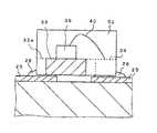
IC、ディスクリート素子等の半導体装置は、図6(A)に示すような封止技術が用いられる。1はシリコン基板、2はシリコン半導体チップ1が固着されるアイランド、3はリード端子、4はボンディングワイヤ、5は封止用の樹脂である。
【0003】
例えばNPN型トランジスタ素子を形成した半導体チップ1は、アイランド2の上に半田等のろう材6を介して固着され、半導体チップ1の周辺に配置したリード端子3とトランジスタ素子のベース電極、エミッタ電極とがそれぞれボンディングワイヤー4で電気的に接続されている。アイランド2がコレクタ電極となる。
【0004】
半導体チップ1をアイランド上に実装した後、エポキシ樹脂等の熱硬化型樹脂4によりトランスファーモールドによって、半導体チップ1とリード端子3の一部を完全に被覆保護し、3端子構造の半導体装置が提供される。樹脂5の外部に導出されたリード端子3はZ字型に折り曲げられる。
上記の半導体装置の製造工程にあっては、アイランド2とリード端子3は、銅素材または鉄素材からなるフープ状あるいは短冊状のリードフレームの状態で供給され、該リードフレームには例えば半導体装置20個分のアイランド2とリード端子3が形成されている。
【0005】
そして、図6(B)を参照して、上金型7及び下金型8によって個々の半導体装置の外形形状に合致した空間であるキャビティ9を構成し、該キャビティの内部にダイボンド及びワイヤボンドを施したリードフレームを設置し、この状態でキャビティ9内に樹脂を注入することによりトランスファーモールドが行われる。更に、樹脂封止した後に前記リードフレームからリード部分他を切断することで半導体装置を個々の素子に分離している。
【0006】
【発明が解決しようとする課題】
第1の課題:
樹脂モールドされた半導体装置は、通常、ガラスエポキシ基板等のプリント基板に実装され、同じくプリント基板上に実装された他の素子と電気的に接続することにより、所望の回路網を構成する。この時、リード端子3が樹脂5の外部に導出された半導体装置では、リード端子3の先端から先端までの距離10を実装面積として占有するので、実装面積が大きいという欠点がある。
【0007】
第2の課題:
トランスファーモールド技術は、上下金型が形成する空間(キャビティ)内に樹脂を注入することによって半導体チップを封止する技術であるが、従来は製造する半導体装置1個毎にキャビティを設け、該キャビティ毎に前記樹脂を注入するための通路を前記金型表面に設けている。封止は、キャビティ及び樹脂を注入する通路を樹脂で充満した状態で樹脂を硬化させることにより行われる。通常の封止技術に用いられるエポキシ樹脂は熱硬化性であり、再利用が不可能であるので、前記樹脂を注入する通路等に残ったままで硬化した樹脂は製品として使用されることなく廃棄処分となる。その為、特に小型化したパッケージの製造においては、半導体製品となる樹脂の量よりは前記廃棄処分になる樹脂の量が多く、その利用効率が悪いという欠点があった。
【0008】
【課題を解決するための手段】
本発明は、上記従来の欠点に鑑み成されたもので、素子搭載部を多数有する共通基板上に半導体チップを搭載する工程と、全体を共通の樹脂層で被覆する工程と、共通の樹脂層の上部を平坦面に加工する工程と、前記樹脂層を素子搭載部毎に、共通基板と共に切断する工程と、を具備するものである。
【0009】
【発明の実施の形態】
以下に本発明の製造方法を詳細に説明する。
第1工程:図1
先ず、共通基板30を準備し、半導体チップのダイボンドとワイヤボンドを行う。第1の形態として金属製リードフレームを示した。図1(A)は共通基板30の平面図であり、図1(B)は図1(A)のAA断面図である。
【0010】
本発明で用いた共通基板30は、半導体チップを搭載するための多数の素子搭載部31、31A....が行・列方向(又はそれらの一方方向にのみ)に複数個繰り返しパターンで配置されており、該多数個の素子搭載部31は、それらの周囲を取り囲む様に配置した枠体部32によって保持されている。
素子搭載部31は、半導体チップを固着するアイランド33と、外部接続用電極となる複数のリード端子34を少なくとも具備する。この時、特定のアイランド33に対しては、その隣に隣接するアイランド33Aに連結するリード端子34が対応して1つの素子搭載部31を構成する。アイランド33とリード端子34との連結部分近傍のリード端子34には、部分的に線幅を細く加工した凹部36を形成している。この様に素子搭載部31を行・列方向に複数配置することで、1本の短冊状の共通基板30に例えば100個の素子搭載部31を配置する。図中D1〜D6は後の工程でダイシングする切断ラインを示し、該切断ラインで囲まれた領域が素子搭載部31である。
【0011】
上記の共通基板30は、例えば、約0.4mm厚の銅系の金属材料で形成された帯状あるいは矩形状のリードフレーム用金属薄板を用意し、このリードフレーム用金属薄板を0.2mm程掘り下げるようにエッチングすることによって得ることができる。裏面側のエッチングされていない箇所を裏板50と定義する。また、1枚の板状材料を裏板50として別に準備し、図1(A)に図示したのと同様のパターンに開口したリードフレームとを張り合わせて形成しても良い。
【0012】
次に、ダイボンド工程とワイヤボンド工程を行う。各アイランド33、33Aの一主面上にAgペースト、半田等の導電ペーストを塗布し、その導電ペーストを介して各アイランド33、33A上に半導体チップ39を固着する。更に、半導体チップ39の表面に形成されたボンディングパッドと、これに対応するリード端子34とをワイヤ40でワイヤボンディングする。ワイヤ40は例えば直径が20μの金線から成る。ここで、ワイヤ40は各アイランド33上に固着した半導体チップ39の表面電極と、その隣に隣接した他のアイランド33Aから延在するリード端子34とを接続する。
【0013】
半導体チップ39が固着されたアイランド33の裏面は、係る半導体チップ39の外部接続用の電極として用いることができる。アイランド33の裏面を接続用端子の1つとして用いる形態は、半導体チップ39として例えばトランジスタ、パワーMOSFET等の、電流経路が垂直方向になる半導体デバイス素子に適している。
【0014】
第2工程:図2(A)(B)
次に、全体を樹脂モールドする。ダイボンドとワイヤボンドを終了した共通基板30を作業台上に設置し、基板30上方からディスペンサー51により所定量の液体樹脂52を滴下(ポッティング)する。樹脂52として例えばCV576AN(松下電工製)を用いた。滴下した液体樹脂52は表面張力を有しているので、基板30全体を被覆するように供給すると、その表面が図2(B)に示すように湾曲面を構成する。樹脂52は、各半導体チップ39...を個別にパッケージングするものではなく、全ての半導体チップ39を共通に被うように形成する。尚、図2(C)に示すように、共通基板30の枠体部32に高さ数mm、幅数mmの環状のダム53を形成しておき、該ダム53で囲まれた領域を満たすように液状の樹脂52を充填するような方法も考えられる。
【0015】
この様にして半導体チップ39を封止した後に、100〜200度、数時間の熱処理(キュア)にて樹脂52を硬化させる。
第3工程:図2(D)
次に、樹脂52の湾曲した表面を削って平坦面を形成する。ダイシング装置を用い、ダイシングブレード54によって樹脂52の表面が共通基板30から一定の高さに揃うように、樹脂52を削る。平坦面は、少なくとも最も外側に位置する半導体チップ39を個別半導体装置に分離したときに、規格化したパッケージサイズの樹脂外形を構成できるように、その端部まで拡張する。前記ブレードには様々な板厚のものが準備されており、用いるブレードの板厚に応じて、複数回繰り返すことで全体を平坦面に形成する。尚、ダイシングブレードの他に砥石による研磨等でも平坦面を形成することが可能である。
【0016】
第4工程:図2(E)
次に、素子搭載部31毎に樹脂52を切断して各々の素子A、素子B、素子C....を分離する。分離に先立ち、図1に示したリードフレームの場合は、あらかじめ裏板50を除去する。裏板50が張り合わせの場合は裏板50を剥がし、一枚の板状材料からハーフエッチングによって形成したものでは、裏板50に相当する箇所を削って、アイランド33とリード端子34のパターンが裏面側からも目視できる状態に形成する。裏板50を削る手法としては、第3工程と同様にダイシングブレードによるダイシングや、他にもエッチング、砥石研磨等があげられる。
【0017】
そして、アイランド33とこの上に固着された半導体チップ39に接続されたリード端子34を囲む領域で分離するような切断ラインD1〜D6で切断することにより、素子搭載部31毎に分割した半導体装置を形成する。切断にはダイシング装置が用いられ、ダイシング装置のブレードによって樹脂52と共通基板30とを同時に切断する。また、切断したリード端子34の他方はアイランド33に連続する突起部として残存する。切断されたリード端子34及び突起部の切断面は、樹脂52の切断面と同一平面を形成し、該同一平面に露出する。ダイシング工程においては裏面側にブルーシート(たとえば、商品名:UVシート、リンテック株式会社製)を貼り付け、前記ダイシングブレードがブルーシートの表面に到達するような切削深さで切断する。この時に、枠体32にあらかじめ形成した合わせマーク37をダイシング装置側で自動認識し、これを位置基準として用いてダイシングする。更に、ダイシングブレードがリード端子33の凹部36上を通過するようにダイシングした。これで、切断後のリード端子33の先端部が先細りの形状となり、樹脂52から容易には抜け落ちない形状に加工できる。
【0018】
図3は斯かる製造方法によって形成した完成後の半導体装置を裏面側からみたときの斜視図である。半導体チップ39とボンディングワイヤ40を含めて、アイランド33とリード端子34が樹脂52でモールドされて、大略直方体のパッケージ形状を形成する。樹脂41の外形寸法は、縦×横×高さが、約0.7mm×1.0mm×0.6mmである。直方体のパッケージ外形を形成する6面のうち、少なくとも4つの側面は樹脂52を切断した(第4工程参照)切断面で構成される。該切断面に沿ってリード端子34の切断面34aが露出する。アイランド33には切断されたリード端子34の名残である突起部33aを有し、これらの突起部の切断面も露出する。リード端子34とアイランド33の裏面側は、樹脂52の表面に露出する。
【0019】
そして、この半導体装置はプリント基板上に半田付けされて実装される。自動実装(チップマウンター)においては、個別に切断した半導体装置を真空吸着コレットにて吸着し、該吸着した半導体装置をプリント基板上の所望箇所に設置するという作業を行う。この時、半導体装置の上側表面(アイランドが露出する面とは反対の表面)が、上記真空吸着コレットの表面に当接するような形で吸着される。そのため、吸着される側の半導体装置には規格化された寸法と精度を維持することが望まれる。本発明では、ポッティングよって湾曲した樹脂52の表面を平坦化する工程(第3工程)を具備するので、吸着される樹脂52表面の寸法と精度を維持でき、自動実装に関してその作業性を損なうことがない。
【0020】
プリント基板上に実装した状態を図4に示す。実装基板24上に形成した素子間接続用のプリント配線25に対して裏面に露出したリード端子34とアイランド33の突起部33aを位置合わせし、半田26等によって両者を接続する。
以下に本発明の第2の実施の形態を説明する。先の実施の形態では支持基板として金属製リードフレームを用いたが、本実施の形態では支持基板としてセラミックやガラスエポキシような絶縁性基板を用いた。
【0021】
図5(A)は、あらかじめ用意した共通基板30の表面に半導体チップ39をダイボンド、ワイヤボンドした状態を示す平面図である。共通基板30の表面には金メッキからなる導電パターンが形成されており、図中D1〜D7はダイシングによって分離する切断ラインを示している。切断ラインD1〜D7で囲まれた矩形エリアが素子搭載部31となる。
【0022】
金メッキのパターンは、半導体チップ39を搭載する為のアイランド部60と、ボンディングワイヤ40のセカンドボンドエリアとなるリード部61とを有しており、素子搭載部31内のアイランド部60とリード部61は連続せず、切断ラインD1〜D7で分離される箇所ではアイランド部60とリード部61とが連続している。更に、切断ラインD1〜D7の交差する箇所(素子搭載部の4隅に相当する)には共通基板30を貫通するスルーホール62が形成され、共通基板30の裏面に形成した、後に表面電極となる導電パターンに接続されている。これにより、アイランド部60とリード部61が各々裏面側の表面電極に電気的に接続される。
【0023】
斯かる共通基板30に対して、ポッティングにより全ての半導体チップ39を樹脂52で被覆する工程、樹脂52の表面を平坦化する工程、素子毎に樹脂52と共通基板とを同時に切断する工程、を経ることにより図5(B)に示したような半導体装置を得る。同図は完成後の半導体装置を示す断面図であり、同じ箇所に同じ符号を伏して説明を省略する。尚、スルーホールを通して共通基板30の表面側のアイランド部60及びリード部61と共通基板30裏面側の表面電極63とが接続されている。表面電極63は金メッキからなる導電パターンである。プリント基板上への実装は、先の実施の形態と同様である。
【0024】
以上の方法によって製造された半導体装置は、以下のメリットを有する。
本発明の製造方法によって製造した半導体装置は、金属製リード端子がパッケージから突出しないので、実装面積を半導体装置のパッケージの大きさと同じ程度の大きさにすることができる。従って、半導体装置の実装面積に対する能動部分(半導体チップ39のチップサイズを意味する)の比である実装有効面積を、図6のものに比べて大幅に増大し、電子機器の軽薄短小化に寄与することができる。
【0025】
トランスファーモールド技術を用いて個々にパッケージングする場合に比べて、無駄にする樹脂を少なくすることができ、材料費の低減につながる。
パッケージの外形をダイシング装置のブレードで切断することにより構成したので、パッケージ外形の寸法精度を向上でき、これによって小型パッケージを精度良く生産することができる。このことは、共通基板30としてリードフレームを用いた場合、アイランド33の面積を増大できることを意味する。即ち、トランスファーモールド技術によるモールド金型とリードフレームとの合わせ精度がプラス・マイナス50μ程度であるのに対して、ダイシング装置によるダイシングブレードとリードフレームとの合わせ精度はプラス・マイナス10μ程度に小さくできる。合わせ精度を小さくできることは、アイランド33の面積を増大して、搭載可能な半導体チップ39のチップ面積を増大できることを意味し、これも上記有効実装面積効率を向上させる。
【0026】
尚、上述した実施形態では、3端子型の半導体装置について説明をしたが、リード端子を3本以上具備するような装置にも適用が可能である。
また、上述した実施の形態では、各アイランドに1つの半導体チップ39を固着したが、1つのアイランドに、例えばトランジスタを複数個固着すること、及び、トタンジスタと縦型パワーMOSFET等の他の素子との複合固着も可能である。
【0027】
さらに、上述した実施の形態では、半導体チップ39にトランジスタを形成したが、例えば、パワーMOSFET、IGBT、HBT等のデバイスを形成した半導体チップであっても、本発明に応用できることは説明するまでもない。加えて、リード端子の本数を増大することでBIP、MOS型等の集積回路等にも応用することができる。
【0028】
【発明の効果】
以上説明したように、本発明によれば、リード端子34がパッケージから突出しない半導体装置を得ることができる。従って、半導体装置を実装したときのデッドスペースを削減し、高密度実装に適した半導体装置を得ることができる。
パッケージの外形をダイシングブレードによる切断面で構成することにより、アイランド33と樹脂52の端面との寸法精度を向上できる。従って、アイランド33の面積を増大して、収納可能な半導体チップ39のチップサイズを増大できる。
【0029】
トランスファーモールド技術を用いて個々にパッケージングする場合に比べて、無駄にする樹脂を少なくすることができ、材料費の低減につながる。
ポッティング技術によって被覆した樹脂52の歪曲表面を平坦化する加工を行った後にダイシングして個々の半導体装置に切り出すので、パッケージ外形の寸法精度を維持することができる。そのため、自動実装に適した半導体装置を製造することができる。
【図面の簡単な説明】
【図1】本発明の製造方法を説明する為の(A)平面図、(B)断面図である。
【図2】本発明の製造方法を説明する為の断面図である。
【図3】本発明の製造方法を説明する為の斜視図である。
【図4】本発明の製造方法を説明する為の断面図である。
【図5】本発明の第2の実施の形態を説明する為の(A)平面図、(B)断面図である。
【図6】従来の半導体装置を説明する図である。[0001]
BACKGROUND OF THE INVENTION
The present invention relates to a semiconductor device, and more particularly, to a method for manufacturing a semiconductor device that can reduce mounting area and improve mounting efficiency.
[0002]
[Prior art]
A semiconductor device such as an IC or a discrete element uses a sealing technique as shown in FIG. 1 is a silicon substrate, 2 is an island to which the
[0003]
For example, a
[0004]
After the
In the manufacturing process of the semiconductor device described above, the
[0005]
Referring to FIG. 6B, the
[0006]
[Problems to be solved by the invention]
First issue:
The resin-molded semiconductor device is usually mounted on a printed board such as a glass epoxy board, and is electrically connected to other elements mounted on the printed board to constitute a desired circuit network. At this time, the semiconductor device in which the
[0007]
Second issue:
The transfer mold technique is a technique for sealing a semiconductor chip by injecting resin into a space (cavity) formed by upper and lower molds. Conventionally, a cavity is provided for each semiconductor device to be manufactured, and the cavity is formed. A passage for injecting the resin is provided on the mold surface every time. The sealing is performed by curing the resin in a state where the cavity and the passage for injecting the resin are filled with the resin. The epoxy resin used in normal sealing technology is thermosetting and cannot be reused. Therefore, the resin cured while remaining in the passage for injecting the resin is discarded without being used as a product. It becomes. Therefore, particularly in the manufacture of a miniaturized package, the amount of the resin to be disposed of is larger than the amount of the resin to be a semiconductor product, and there is a disadvantage that the utilization efficiency is poor.
[0008]
[Means for Solving the Problems]
The present invention has been made in view of the above-described conventional drawbacks, and includes a step of mounting a semiconductor chip on a common substrate having a large number of element mounting portions, a step of covering the whole with a common resin layer, and a common resin layer. And a step of cutting the resin layer together with a common substrate for each element mounting portion.
[0009]
DETAILED DESCRIPTION OF THE INVENTION
The production method of the present invention will be described in detail below.
First step: FIG.
First, the
[0010]
The
The
[0011]
For the
[0012]
Next, a die bonding process and a wire bonding process are performed. A conductive paste such as Ag paste or solder is applied on one main surface of each
[0013]
The back surface of the
[0014]
Second step: FIGS. 2A and 2B
Next, the whole is resin-molded. The
[0015]
After sealing the
Third step: FIG. 2 (D)
Next, the curved surface of the
[0016]
Fourth step: FIG. 2 (E)
Next, the
[0017]
And the semiconductor device divided | segmented for every
[0018]
FIG. 3 is a perspective view of the completed semiconductor device formed by such a manufacturing method as seen from the back side. The
[0019]
The semiconductor device is mounted by soldering on a printed circuit board. In automatic mounting (chip mounter), a semiconductor device cut individually is sucked by a vacuum suction collet, and the sucked semiconductor device is installed at a desired location on a printed board. At this time, the upper surface of the semiconductor device (the surface opposite to the surface from which the island is exposed) is adsorbed in such a manner as to come into contact with the surface of the vacuum adsorption collet. For this reason, it is desired to maintain standardized dimensions and accuracy for the semiconductor device to be attracted. In the present invention, since the step (third step) for flattening the surface of the
[0020]
The state mounted on the printed circuit board is shown in FIG. The
The second embodiment of the present invention will be described below. In the previous embodiment, a metal lead frame was used as the support substrate, but in this embodiment, an insulating substrate such as ceramic or glass epoxy was used as the support substrate.
[0021]
FIG. 5A is a plan view showing a state in which the
[0022]
The gold plating pattern has an
[0023]
A step of covering all the semiconductor chips 39 with the
[0024]
The semiconductor device manufactured by the above method has the following merits.
In the semiconductor device manufactured by the manufacturing method of the present invention, since the metal lead terminals do not protrude from the package, the mounting area can be made as large as the size of the package of the semiconductor device. Therefore, the mounting effective area, which is the ratio of the active portion (meaning the chip size of the semiconductor chip 39) to the mounting area of the semiconductor device, is greatly increased compared to that of FIG. can do.
[0025]
Compared to the case of individual packaging using transfer molding technology, the amount of resin that is wasted can be reduced, leading to a reduction in material costs.
Since the outer shape of the package is cut by the blade of the dicing apparatus, the dimensional accuracy of the outer shape of the package can be improved, and a small package can be produced with high accuracy. This means that when the lead frame is used as the
[0026]
In the above-described embodiment, the three-terminal type semiconductor device has been described. However, the present invention can also be applied to a device having three or more lead terminals.
In the above-described embodiment, one
[0027]
Further, in the above-described embodiment, the transistor is formed on the
[0028]
【The invention's effect】
As described above, according to the present invention, a semiconductor device in which the
By configuring the outer shape of the package with a cut surface by a dicing blade, the dimensional accuracy between the
[0029]
Compared to the case of individual packaging using transfer molding technology, the amount of resin that is wasted can be reduced, leading to a reduction in material costs.
Since the distortion surface of the
[Brief description of the drawings]
1A is a plan view and FIG. 1B is a cross-sectional view for explaining a manufacturing method of the present invention.
FIG. 2 is a cross-sectional view for explaining the manufacturing method of the present invention.
FIG. 3 is a perspective view for explaining the manufacturing method of the present invention.
FIG. 4 is a cross-sectional view for explaining the manufacturing method of the present invention.
5A is a plan view and FIG. 5B is a sectional view for explaining a second embodiment of the present invention.
FIG. 6 is a diagram illustrating a conventional semiconductor device.
Claims (5)
Translated fromJapanese前記アイランドと成る凸状パターンに半導体チップを固着するとともに、前記半導体チップと前記リード端子と成る凸状パターンを電気的に接続し、While fixing the semiconductor chip to the convex pattern to be the island, electrically connecting the semiconductor chip and the convex pattern to be the lead terminal,
前記半導体チップを封止するように、前記金属薄板を樹脂で封止し、The metal thin plate is sealed with a resin so as to seal the semiconductor chip,
前記封止を目的として設けられた前記樹脂の裏側に位置する前記金属薄板を取り除き、前記樹脂の裏側から前記アイランドと成る凸状パターンと前記リード端子となる凸状パターンが目視できるようにし、The metal thin plate located on the back side of the resin provided for the purpose of sealing is removed, so that the convex pattern serving as the island and the convex pattern serving as the lead terminal can be seen from the back side of the resin,
前記アイランドと成る凸状パターンと前記リード端子となる凸状パターンから成るユニットを囲む領域で、個別半導体装置として分離する事を特徴とした半導体装置の製造方法。A method of manufacturing a semiconductor device, characterized in that the semiconductor device is separated as an individual semiconductor device in a region surrounding a unit composed of the convex pattern serving as the island and the convex pattern serving as the lead terminal.
Priority Applications (5)
| Application Number | Priority Date | Filing Date | Title |
|---|---|---|---|
| JP35746697AJP3819574B2 (en) | 1997-12-25 | 1997-12-25 | Manufacturing method of semiconductor device |
| TW87118397ATW434755B (en) | 1997-12-25 | 1998-11-05 | Method for making semiconductors |
| US09/219,508US6080602A (en) | 1997-12-25 | 1998-12-23 | Method of producing a semiconductor device using a reduced mounting area |
| KR1019980058668AKR100284459B1 (en) | 1997-12-25 | 1998-12-24 | Manufacturing Method of Semiconductor Device |
| US09/584,076US6451628B1 (en) | 1997-12-25 | 2000-06-01 | Method fabricating a semiconductor device with a decreased mounting area |
Applications Claiming Priority (1)
| Application Number | Priority Date | Filing Date | Title |
|---|---|---|---|
| JP35746697AJP3819574B2 (en) | 1997-12-25 | 1997-12-25 | Manufacturing method of semiconductor device |
Publications (2)
| Publication Number | Publication Date |
|---|---|
| JPH11186301A JPH11186301A (en) | 1999-07-09 |
| JP3819574B2true JP3819574B2 (en) | 2006-09-13 |
Family
ID=18454275
Family Applications (1)
| Application Number | Title | Priority Date | Filing Date |
|---|---|---|---|
| JP35746697AExpired - LifetimeJP3819574B2 (en) | 1997-12-25 | 1997-12-25 | Manufacturing method of semiconductor device |
Country Status (4)
| Country | Link |
|---|---|
| US (2) | US6080602A (en) |
| JP (1) | JP3819574B2 (en) |
| KR (1) | KR100284459B1 (en) |
| TW (1) | TW434755B (en) |
Cited By (54)
| Publication number | Priority date | Publication date | Assignee | Title |
|---|---|---|---|---|
| EP1614537A1 (en) | 2004-07-07 | 2006-01-11 | Fuji Photo Film Co., Ltd. | Lithographic printing plate precursor and lithographic printing method |
| EP1619023A2 (en) | 2004-07-20 | 2006-01-25 | Fuji Photo Film Co., Ltd. | Image forming material |
| EP1621338A1 (en) | 2004-07-27 | 2006-02-01 | Fuji Photo Film Co., Ltd. | Lithographic printing plate precursor and lithographic printing method |
| EP1630602A2 (en) | 2004-08-31 | 2006-03-01 | Fuji Photo Film Co., Ltd. | Polymerizable composition, hydrophilic film formed by curing said composition and planographic printing plate precursor |
| EP1685957A2 (en) | 2005-01-26 | 2006-08-02 | Fuji Photo Film Co., Ltd. | Lithographic printing plate precursor, lithographic printing method and packaged body of lithographic printing plate precursors |
| EP1754597A2 (en) | 2005-08-19 | 2007-02-21 | Fuji Photo Film Co., Ltd. | Lithographic printing plate precursor and lithographic printing process |
| EP1755002A2 (en) | 2005-08-18 | 2007-02-21 | Fuji Photo Film Co., Ltd. | Manufacturing method of lithographic printing plate and manufacturing apparatus of lithographic printing plate |
| EP1939687A2 (en) | 2006-12-26 | 2008-07-02 | FUJIFILM Corporation | Polymerizable composition, lithographic printing plate precursor and lithographic printing method |
| EP1947514A2 (en) | 2007-01-17 | 2008-07-23 | FUJIFILM Corporation | Method for preparation of lithographic printing plate |
| EP1956428A2 (en) | 2007-02-06 | 2008-08-13 | FUJIFILM Corporation | Photosensitive composition, lithographic printing plate precursor, lithographic printing method, and cyanine dyes |
| EP1972440A2 (en) | 2007-03-23 | 2008-09-24 | FUJIFILM Corporation | Negative lithographic printing plate precursor and lithographic printing method using the same |
| EP1972439A2 (en) | 2007-03-20 | 2008-09-24 | FUJIFILM Corporation | On-press developable lithographic printing plate precursor |
| EP1972438A1 (en) | 2007-03-20 | 2008-09-24 | FUJIFILM Corporation | Lithographic printing plate precursor and method of preparing lithographic printing plate |
| EP1975706A2 (en) | 2007-03-30 | 2008-10-01 | FUJIFILM Corporation | Lithographic printing plate precursor |
| EP1975710A2 (en) | 2007-03-30 | 2008-10-01 | FUJIFILM Corporation | Plate-making method of lithographic printing plate precursor |
| EP1974914A2 (en) | 2007-03-29 | 2008-10-01 | FUJIFILM Corporation | Lithographic printing plate precursor and method of preparing lithographic printing plate |
| EP1992482A2 (en) | 2007-05-18 | 2008-11-19 | FUJIFILM Corporation | Planographic printing plate precursor and printing method using the same |
| EP1992989A1 (en) | 2004-12-27 | 2008-11-19 | FUJIFILM Corporation | Lithographic printing plate precursor |
| EP2006091A2 (en) | 2007-06-22 | 2008-12-24 | FUJIFILM Corporation | Lithographic printing plate precursor and plate making method |
| EP2006738A2 (en) | 2007-06-21 | 2008-12-24 | Fujifilm Corporation | Lithographic printing plate precursor and lithographic printing method |
| EP2011643A2 (en) | 2007-07-02 | 2009-01-07 | FUJIFILM Corporation | Planographic printing plate precursor and printing method using the same |
| EP2042312A2 (en) | 2007-09-28 | 2009-04-01 | FUJIFILM Corporation | Processing method of lithographic printing plate precursor |
| EP2042311A1 (en) | 2007-09-28 | 2009-04-01 | FUJIFILM Corporation | Lithographic printing plate precursor, method of preparing lithographic printing plate and lithographic printing method |
| EP2042923A2 (en) | 2007-09-28 | 2009-04-01 | FUJIFILM Corporation | Image-forming method and lithographic printing plate precursor |
| EP2045662A2 (en) | 2007-09-28 | 2009-04-08 | FUJIFILM Corporation | Lithographic printing plate precursor and method of preparing lithographic printing plate |
| EP2048000A2 (en) | 2007-09-18 | 2009-04-15 | FUJIFILM Corporation | Plate making method of lithographic printing plate precursor |
| EP2070696A1 (en) | 2007-12-10 | 2009-06-17 | FUJIFILM Corporation | Method of preparing lithographic printing plate and lithographic printing plate precursor |
| EP2078984A1 (en) | 2008-01-11 | 2009-07-15 | Fujifilm Corporation | Lithographic printing plate precursor, method of preparing lithographic printing plate and lithographic printing method |
| EP2082875A1 (en) | 2008-01-22 | 2009-07-29 | FUJIFILM Corporation | Lithographic printing plate precursor and plate making method thereof |
| EP2088468A1 (en) | 2008-02-06 | 2009-08-12 | FUJIFILM Corporation | Method of preparing lithographic printing plate and lithographic printing plate precursor |
| EP2090933A1 (en) | 2008-02-05 | 2009-08-19 | FUJIFILM Corporation | Lithographic printing plate precursor and printing method |
| EP2093055A1 (en) | 2003-03-26 | 2009-08-26 | Fujifilm Corporation | Lithographic printing method and presensitized plate |
| EP2101218A1 (en) | 2008-03-10 | 2009-09-16 | FUJIFILM Corporation | Method for preparing lithographic printing plate and lithographic printing plate precursor |
| EP2105797A1 (en) | 2008-03-25 | 2009-09-30 | FUJIFILM Corporation | Lithographic printing plate precursor |
| EP2105800A2 (en) | 2008-03-25 | 2009-09-30 | FUJIFILM Corporation | Processing solution for preparing lithographic printing plate and processing method of lithographic printing plate precursor |
| EP2105796A1 (en) | 2008-03-28 | 2009-09-30 | FUJIFILM Corporation | Plate-making method of lithographic printing plate |
| EP2105297A1 (en) | 2008-03-25 | 2009-09-30 | FUJIFILM Corporation | Planographic printing plate precursor and plate making method using the same |
| WO2009119430A1 (en) | 2008-03-25 | 2009-10-01 | 富士フイルム株式会社 | Process for producing lithographic printing plate |
| EP2107422A1 (en) | 2008-03-31 | 2009-10-07 | FUJIFILM Corporation | Method for preparing lithographic printing plate |
| EP2112555A2 (en) | 2008-03-27 | 2009-10-28 | FUJIFILM Corporation | Lithographic printing plate precursor |
| EP2145772A2 (en) | 2008-07-16 | 2010-01-20 | FUJIFILM Corporation | Method of manufacturing aluminum alloy plate for lithographic printing plate, aluminum alloy plate for lithographic printing plate, lithographic printing plate support and presensitized plate |
| EP2163949A1 (en) | 2008-09-12 | 2010-03-17 | FUJIFILM Corporation | Developer for lithographic printing plate precursor and process for producing lithographic printing plate |
| EP2165830A1 (en) | 2008-09-22 | 2010-03-24 | Fujifilm Corporation | Lithographic printing plate precursor and printing method using the same |
| EP2168765A2 (en) | 2008-09-25 | 2010-03-31 | FUJIFILM Corporation | Lithographic printing plate precursor and process for producing lithographic printing plate |
| EP2168767A1 (en) | 2008-09-24 | 2010-03-31 | Fujifilm Corporation | Method of preparing lithographic printing plate |
| EP2168766A1 (en) | 2008-09-26 | 2010-03-31 | FUJIFILM Corporation | Process for making lithographic printing plate |
| WO2010035697A1 (en) | 2008-09-24 | 2010-04-01 | 富士フイルム株式会社 | Process for producing lithographic printing plate |
| EP2177357A2 (en) | 2008-08-29 | 2010-04-21 | Fujifilm Corporation | Negative-working lithographic printing plate precursor and method of lithographic printing using same |
| EP2184642A2 (en) | 2008-09-30 | 2010-05-12 | FUJIFILM Corporation | Lithographic printing plate precursor and method of preparing lithographic printing plate |
| WO2010061869A1 (en) | 2008-11-26 | 2010-06-03 | 富士フイルム株式会社 | Method for manufacturing lithographic printing plate, developer for original lithographic printing plate, and replenisher for developing original lithographic printing plate |
| EP2246741A1 (en) | 2004-05-19 | 2010-11-03 | Fujifilm Corporation | Image recording method |
| EP2295247A1 (en) | 2003-07-07 | 2011-03-16 | Fujifilm Corporation | Lithographic printing plate precursor and lithographic printing method |
| EP2380737A1 (en) | 2007-10-29 | 2011-10-26 | Fujifilm Corporation | Lithographic printing plate precursor |
| EP2503393A1 (en) | 2006-12-28 | 2012-09-26 | Fujifilm Corporation | Method for preparation of lithographic printing plate |
Families Citing this family (40)
| Publication number | Priority date | Publication date | Assignee | Title |
|---|---|---|---|---|
| JP3877401B2 (en) | 1997-03-10 | 2007-02-07 | 三洋電機株式会社 | Manufacturing method of semiconductor device |
| MY122101A (en)* | 1997-03-28 | 2006-03-31 | Rohm Co Ltd | Lead frame and semiconductor device made by using it |
| JP3819574B2 (en)* | 1997-12-25 | 2006-09-13 | 三洋電機株式会社 | Manufacturing method of semiconductor device |
| US6284570B1 (en)* | 1998-12-28 | 2001-09-04 | Semiconductor Components Industries Llc | Method of manufacturing a semiconductor component from a conductive substrate containing a plurality of vias |
| US6434365B1 (en)* | 1998-12-29 | 2002-08-13 | Thomson Licensing Sa | Providing initial power estimate to wireless telephone handsets |
| JP4803855B2 (en)* | 1999-02-09 | 2011-10-26 | 三洋電機株式会社 | Manufacturing method of semiconductor device |
| US6267282B1 (en)* | 1999-04-01 | 2001-07-31 | Agere Systems Optoelectronics Guardian Corp. | Method and apparatus for handling laser bars |
| JP3339838B2 (en) | 1999-06-07 | 2002-10-28 | ローム株式会社 | Semiconductor device and method of manufacturing the same |
| US6338980B1 (en)* | 1999-08-13 | 2002-01-15 | Citizen Watch Co., Ltd. | Method for manufacturing chip-scale package and manufacturing IC chip |
| JP2001185651A (en) | 1999-12-27 | 2001-07-06 | Matsushita Electronics Industry Corp | Semiconductor device and manufacturing method therefor |
| KR100324283B1 (en)* | 2000-02-23 | 2002-02-21 | 구본준, 론 위라하디락사 | Tape Carrier Package and Method of Fabricating the same |
| JP3741935B2 (en)* | 2000-05-11 | 2006-02-01 | シャープ株式会社 | Optical coupling element |
| JP2002026182A (en)* | 2000-07-07 | 2002-01-25 | Sanyo Electric Co Ltd | Method for manufacturing semiconductor device |
| JP3738176B2 (en)* | 2000-08-03 | 2006-01-25 | 三洋電機株式会社 | Manufacturing method of semiconductor device |
| KR20020031716A (en)* | 2000-10-23 | 2002-05-03 | 마이클 디. 오브라이언 | Method for singulation semiconductor package |
| JP3420748B2 (en) | 2000-12-14 | 2003-06-30 | 松下電器産業株式会社 | Semiconductor device and manufacturing method thereof |
| JP3958532B2 (en)* | 2001-04-16 | 2007-08-15 | ローム株式会社 | Manufacturing method of chip resistor |
| JP2003023134A (en)* | 2001-07-09 | 2003-01-24 | Hitachi Ltd | Semiconductor device and method of manufacturing the same |
| US6951980B2 (en)* | 2001-09-29 | 2005-10-04 | Texas Instruments Incorporated | Package for an electrical device |
| US6884663B2 (en)* | 2002-01-07 | 2005-04-26 | Delphon Industries, Llc | Method for reconstructing an integrated circuit package using lapping |
| US6908784B1 (en)* | 2002-03-06 | 2005-06-21 | Micron Technology, Inc. | Method for fabricating encapsulated semiconductor components |
| TW544894B (en)* | 2002-04-10 | 2003-08-01 | Siliconware Precision Industries Co Ltd | Chip carrier with dam bar |
| US20110005667A1 (en)* | 2002-05-10 | 2011-01-13 | Delphon Industries LLC | Multiple segment vacuum release handling device |
| US20030209847A1 (en)* | 2002-05-10 | 2003-11-13 | Allison Claudia Leigh | Handling device comprising multiple immobilization segments |
| US6903442B2 (en)* | 2002-08-29 | 2005-06-07 | Micron Technology, Inc. | Semiconductor component having backside pin contacts |
| US7388294B2 (en)* | 2003-01-27 | 2008-06-17 | Micron Technology, Inc. | Semiconductor components having stacked dice |
| US6841883B1 (en)* | 2003-03-31 | 2005-01-11 | Micron Technology, Inc. | Multi-dice chip scale semiconductor components and wafer level methods of fabrication |
| JP4152855B2 (en)* | 2003-10-01 | 2008-09-17 | リンテック株式会社 | A method for manufacturing a resin-encapsulated electronic device. |
| JP5136552B2 (en)* | 2007-06-13 | 2013-02-06 | 富士通株式会社 | How to remove electronic components from carrier tape |
| KR100991226B1 (en) | 2008-06-25 | 2010-11-01 | 주식회사 씨엠아이 | Chip package assembly having a metal cap and a method of manufacturing the same |
| JPWO2010140604A1 (en) | 2009-06-05 | 2012-11-22 | 先端フォトニクス株式会社 | Submount, optical module provided with the same, and method of manufacturing submount |
| WO2011077962A1 (en) | 2009-12-24 | 2011-06-30 | 株式会社 村田製作所 | Electronic component manufacturing method |
| JP2011249530A (en)* | 2010-05-26 | 2011-12-08 | Murata Mfg Co Ltd | Manufacturing method of module substrate |
| JP5252007B2 (en)* | 2011-03-08 | 2013-07-31 | 株式会社村田製作所 | Manufacturing method of electronic parts |
| CN103000768A (en)* | 2011-09-09 | 2013-03-27 | 展晶科技(深圳)有限公司 | Method for manufacturing light emitting diode packaging structure |
| CN103165765A (en)* | 2011-12-17 | 2013-06-19 | 展晶科技(深圳)有限公司 | Light-emitting diode manufacturing method |
| US9418907B2 (en) | 2013-01-22 | 2016-08-16 | Ps5 Luxco S.A.R.L. | Method for manufacturing semiconductor device |
| US9355945B1 (en)* | 2015-09-02 | 2016-05-31 | Freescale Semiconductor, Inc. | Semiconductor device with heat-dissipating lead frame |
| CN113937049B (en)* | 2020-06-29 | 2025-02-18 | 重庆康佳光电科技有限公司 | Microfluidic chip and its manufacturing method, transfer head and its manufacturing method |
| KR102793856B1 (en)* | 2024-05-20 | 2025-04-11 | 주식회사 에이치이엠씨 | Semiconductor package substrate manufacturing method, semiconductor package substrate |
Family Cites Families (20)
| Publication number | Priority date | Publication date | Assignee | Title |
|---|---|---|---|---|
| DE619636C (en)* | 1934-03-03 | 1935-10-04 | Siemens Ag | Automatic switching device for electrically heated devices whose heating coil is temporarily connected to a high voltage for the purpose of rapid heating |
| JPS56135984A (en)* | 1980-03-27 | 1981-10-23 | Matsushita Electric Ind Co Ltd | Manufacture of leadless light emitting diode chip |
| DE3619636A1 (en) | 1986-06-11 | 1987-12-17 | Bosch Gmbh Robert | Housing for integrated circuits |
| US5200362A (en)* | 1989-09-06 | 1993-04-06 | Motorola, Inc. | Method of attaching conductive traces to an encapsulated semiconductor die using a removable transfer film |
| JP3270214B2 (en)* | 1993-09-29 | 2002-04-02 | 日本碍子株式会社 | Orthogonal core current limiter |
| JPH07240366A (en)* | 1994-03-02 | 1995-09-12 | Nikon Corp | Exposure equipment |
| JP3247384B2 (en)* | 1994-03-18 | 2002-01-15 | 日立化成工業株式会社 | Semiconductor package manufacturing method and semiconductor package |
| JP3127195B2 (en)* | 1994-12-06 | 2001-01-22 | シャープ株式会社 | Light emitting device and method of manufacturing the same |
| US5652185A (en)* | 1995-04-07 | 1997-07-29 | National Semiconductor Corporation | Maximized substrate design for grid array based assemblies |
| US5832600A (en)* | 1995-06-06 | 1998-11-10 | Seiko Epson Corporation | Method of mounting electronic parts |
| JP3146452B2 (en)* | 1995-08-11 | 2001-03-19 | スタンレー電気株式会社 | Surface mount type LED element and method of manufacturing the same |
| JP3507251B2 (en)* | 1995-09-01 | 2004-03-15 | キヤノン株式会社 | Optical sensor IC package and method of assembling the same |
| JP3170199B2 (en)* | 1996-03-15 | 2001-05-28 | 株式会社東芝 | Semiconductor device, method of manufacturing the same, and substrate frame |
| JP3656316B2 (en)* | 1996-04-09 | 2005-06-08 | 日亜化学工業株式会社 | Chip-type LED and manufacturing method thereof |
| US5776798A (en)* | 1996-09-04 | 1998-07-07 | Motorola, Inc. | Semiconductor package and method thereof |
| JPH10135254A (en)* | 1996-11-01 | 1998-05-22 | Sony Corp | Semiconductor device and manufacturing method thereof |
| US5830800A (en)* | 1997-04-11 | 1998-11-03 | Compeq Manufacturing Company Ltd. | Packaging method for a ball grid array integrated circuit without utilizing a base plate |
| JP3819574B2 (en)* | 1997-12-25 | 2006-09-13 | 三洋電機株式会社 | Manufacturing method of semiconductor device |
| JPH11204555A (en)* | 1998-01-19 | 1999-07-30 | Sony Corp | Semiconductor package and manufacture of the same |
| JP3877454B2 (en)* | 1998-11-27 | 2007-02-07 | 三洋電機株式会社 | Manufacturing method of semiconductor device |
- 1997
- 1997-12-25JPJP35746697Apatent/JP3819574B2/ennot_activeExpired - Lifetime
- 1998
- 1998-11-05TWTW87118397Apatent/TW434755B/ennot_activeIP Right Cessation
- 1998-12-23USUS09/219,508patent/US6080602A/ennot_activeExpired - Lifetime
- 1998-12-24KRKR1019980058668Apatent/KR100284459B1/ennot_activeExpired - Lifetime
- 2000
- 2000-06-01USUS09/584,076patent/US6451628B1/ennot_activeExpired - Lifetime
Cited By (56)
| Publication number | Priority date | Publication date | Assignee | Title |
|---|---|---|---|---|
| EP2093055A1 (en) | 2003-03-26 | 2009-08-26 | Fujifilm Corporation | Lithographic printing method and presensitized plate |
| EP2295247A1 (en) | 2003-07-07 | 2011-03-16 | Fujifilm Corporation | Lithographic printing plate precursor and lithographic printing method |
| EP2246741A1 (en) | 2004-05-19 | 2010-11-03 | Fujifilm Corporation | Image recording method |
| EP1614537A1 (en) | 2004-07-07 | 2006-01-11 | Fuji Photo Film Co., Ltd. | Lithographic printing plate precursor and lithographic printing method |
| EP1619023A2 (en) | 2004-07-20 | 2006-01-25 | Fuji Photo Film Co., Ltd. | Image forming material |
| EP1621338A1 (en) | 2004-07-27 | 2006-02-01 | Fuji Photo Film Co., Ltd. | Lithographic printing plate precursor and lithographic printing method |
| EP1630602A2 (en) | 2004-08-31 | 2006-03-01 | Fuji Photo Film Co., Ltd. | Polymerizable composition, hydrophilic film formed by curing said composition and planographic printing plate precursor |
| EP1992989A1 (en) | 2004-12-27 | 2008-11-19 | FUJIFILM Corporation | Lithographic printing plate precursor |
| EP1685957A2 (en) | 2005-01-26 | 2006-08-02 | Fuji Photo Film Co., Ltd. | Lithographic printing plate precursor, lithographic printing method and packaged body of lithographic printing plate precursors |
| EP2306246A1 (en) | 2005-08-18 | 2011-04-06 | Fujifilm Corporation | Manufacturing method of lithographic printing plate |
| EP1755002A2 (en) | 2005-08-18 | 2007-02-21 | Fuji Photo Film Co., Ltd. | Manufacturing method of lithographic printing plate and manufacturing apparatus of lithographic printing plate |
| EP1754597A2 (en) | 2005-08-19 | 2007-02-21 | Fuji Photo Film Co., Ltd. | Lithographic printing plate precursor and lithographic printing process |
| EP1939687A2 (en) | 2006-12-26 | 2008-07-02 | FUJIFILM Corporation | Polymerizable composition, lithographic printing plate precursor and lithographic printing method |
| EP2503393A1 (en) | 2006-12-28 | 2012-09-26 | Fujifilm Corporation | Method for preparation of lithographic printing plate |
| EP1947514A2 (en) | 2007-01-17 | 2008-07-23 | FUJIFILM Corporation | Method for preparation of lithographic printing plate |
| EP2592475A1 (en) | 2007-02-06 | 2013-05-15 | Fujifilm Corporation | Photosensitive composition, lithographic printing plate precursor, lithographic printing method, and novel cyanine dyes |
| EP1956428A2 (en) | 2007-02-06 | 2008-08-13 | FUJIFILM Corporation | Photosensitive composition, lithographic printing plate precursor, lithographic printing method, and cyanine dyes |
| EP1972438A1 (en) | 2007-03-20 | 2008-09-24 | FUJIFILM Corporation | Lithographic printing plate precursor and method of preparing lithographic printing plate |
| EP1972439A2 (en) | 2007-03-20 | 2008-09-24 | FUJIFILM Corporation | On-press developable lithographic printing plate precursor |
| EP1972440A2 (en) | 2007-03-23 | 2008-09-24 | FUJIFILM Corporation | Negative lithographic printing plate precursor and lithographic printing method using the same |
| EP1974914A2 (en) | 2007-03-29 | 2008-10-01 | FUJIFILM Corporation | Lithographic printing plate precursor and method of preparing lithographic printing plate |
| EP1975710A2 (en) | 2007-03-30 | 2008-10-01 | FUJIFILM Corporation | Plate-making method of lithographic printing plate precursor |
| EP1975706A2 (en) | 2007-03-30 | 2008-10-01 | FUJIFILM Corporation | Lithographic printing plate precursor |
| EP1992482A2 (en) | 2007-05-18 | 2008-11-19 | FUJIFILM Corporation | Planographic printing plate precursor and printing method using the same |
| EP2006738A2 (en) | 2007-06-21 | 2008-12-24 | Fujifilm Corporation | Lithographic printing plate precursor and lithographic printing method |
| EP2006091A2 (en) | 2007-06-22 | 2008-12-24 | FUJIFILM Corporation | Lithographic printing plate precursor and plate making method |
| EP2011643A2 (en) | 2007-07-02 | 2009-01-07 | FUJIFILM Corporation | Planographic printing plate precursor and printing method using the same |
| EP2048000A2 (en) | 2007-09-18 | 2009-04-15 | FUJIFILM Corporation | Plate making method of lithographic printing plate precursor |
| EP2045662A2 (en) | 2007-09-28 | 2009-04-08 | FUJIFILM Corporation | Lithographic printing plate precursor and method of preparing lithographic printing plate |
| EP2042923A2 (en) | 2007-09-28 | 2009-04-01 | FUJIFILM Corporation | Image-forming method and lithographic printing plate precursor |
| EP2042311A1 (en) | 2007-09-28 | 2009-04-01 | FUJIFILM Corporation | Lithographic printing plate precursor, method of preparing lithographic printing plate and lithographic printing method |
| EP2042312A2 (en) | 2007-09-28 | 2009-04-01 | FUJIFILM Corporation | Processing method of lithographic printing plate precursor |
| EP2380737A1 (en) | 2007-10-29 | 2011-10-26 | Fujifilm Corporation | Lithographic printing plate precursor |
| EP2070696A1 (en) | 2007-12-10 | 2009-06-17 | FUJIFILM Corporation | Method of preparing lithographic printing plate and lithographic printing plate precursor |
| EP2078984A1 (en) | 2008-01-11 | 2009-07-15 | Fujifilm Corporation | Lithographic printing plate precursor, method of preparing lithographic printing plate and lithographic printing method |
| EP2082875A1 (en) | 2008-01-22 | 2009-07-29 | FUJIFILM Corporation | Lithographic printing plate precursor and plate making method thereof |
| EP2090933A1 (en) | 2008-02-05 | 2009-08-19 | FUJIFILM Corporation | Lithographic printing plate precursor and printing method |
| EP2088468A1 (en) | 2008-02-06 | 2009-08-12 | FUJIFILM Corporation | Method of preparing lithographic printing plate and lithographic printing plate precursor |
| EP2101218A1 (en) | 2008-03-10 | 2009-09-16 | FUJIFILM Corporation | Method for preparing lithographic printing plate and lithographic printing plate precursor |
| WO2009119430A1 (en) | 2008-03-25 | 2009-10-01 | 富士フイルム株式会社 | Process for producing lithographic printing plate |
| EP2105297A1 (en) | 2008-03-25 | 2009-09-30 | FUJIFILM Corporation | Planographic printing plate precursor and plate making method using the same |
| EP2105797A1 (en) | 2008-03-25 | 2009-09-30 | FUJIFILM Corporation | Lithographic printing plate precursor |
| EP2105800A2 (en) | 2008-03-25 | 2009-09-30 | FUJIFILM Corporation | Processing solution for preparing lithographic printing plate and processing method of lithographic printing plate precursor |
| EP2112555A2 (en) | 2008-03-27 | 2009-10-28 | FUJIFILM Corporation | Lithographic printing plate precursor |
| EP2105796A1 (en) | 2008-03-28 | 2009-09-30 | FUJIFILM Corporation | Plate-making method of lithographic printing plate |
| EP2107422A1 (en) | 2008-03-31 | 2009-10-07 | FUJIFILM Corporation | Method for preparing lithographic printing plate |
| EP2145772A2 (en) | 2008-07-16 | 2010-01-20 | FUJIFILM Corporation | Method of manufacturing aluminum alloy plate for lithographic printing plate, aluminum alloy plate for lithographic printing plate, lithographic printing plate support and presensitized plate |
| EP2177357A2 (en) | 2008-08-29 | 2010-04-21 | Fujifilm Corporation | Negative-working lithographic printing plate precursor and method of lithographic printing using same |
| EP2163949A1 (en) | 2008-09-12 | 2010-03-17 | FUJIFILM Corporation | Developer for lithographic printing plate precursor and process for producing lithographic printing plate |
| EP2165830A1 (en) | 2008-09-22 | 2010-03-24 | Fujifilm Corporation | Lithographic printing plate precursor and printing method using the same |
| WO2010035697A1 (en) | 2008-09-24 | 2010-04-01 | 富士フイルム株式会社 | Process for producing lithographic printing plate |
| EP2168767A1 (en) | 2008-09-24 | 2010-03-31 | Fujifilm Corporation | Method of preparing lithographic printing plate |
| EP2168765A2 (en) | 2008-09-25 | 2010-03-31 | FUJIFILM Corporation | Lithographic printing plate precursor and process for producing lithographic printing plate |
| EP2168766A1 (en) | 2008-09-26 | 2010-03-31 | FUJIFILM Corporation | Process for making lithographic printing plate |
| EP2184642A2 (en) | 2008-09-30 | 2010-05-12 | FUJIFILM Corporation | Lithographic printing plate precursor and method of preparing lithographic printing plate |
| WO2010061869A1 (en) | 2008-11-26 | 2010-06-03 | 富士フイルム株式会社 | Method for manufacturing lithographic printing plate, developer for original lithographic printing plate, and replenisher for developing original lithographic printing plate |
Also Published As
| Publication number | Publication date |
|---|---|
| TW434755B (en) | 2001-05-16 |
| KR100284459B1 (en) | 2001-04-02 |
| JPH11186301A (en) | 1999-07-09 |
| US6451628B1 (en) | 2002-09-17 |
| KR19990063463A (en) | 1999-07-26 |
| US6080602A (en) | 2000-06-27 |
Similar Documents
| Publication | Publication Date | Title |
|---|---|---|
| JP3819574B2 (en) | Manufacturing method of semiconductor device | |
| JP4408475B2 (en) | Semiconductor devices that do not use bonding wires | |
| JP3877454B2 (en) | Manufacturing method of semiconductor device | |
| JP3877409B2 (en) | Manufacturing method of semiconductor device | |
| JP3877410B2 (en) | Manufacturing method of semiconductor device | |
| JP4803855B2 (en) | Manufacturing method of semiconductor device | |
| JP3269025B2 (en) | Semiconductor device and manufacturing method thereof | |
| JP4073098B2 (en) | Manufacturing method of semiconductor device | |
| JP3877405B2 (en) | Manufacturing method of semiconductor device | |
| JP3877402B2 (en) | Manufacturing method of semiconductor device | |
| JP3831504B2 (en) | Lead frame | |
| JP4334047B2 (en) | Semiconductor device and manufacturing method thereof | |
| JP3710942B2 (en) | Manufacturing method of semiconductor device | |
| JP3203228B2 (en) | Semiconductor device and manufacturing method thereof | |
| JP2003046053A (en) | Semiconductor device and manufacturing method therefor | |
| JP4165952B2 (en) | Semiconductor device | |
| JP2009065201A (en) | Method of manufacturing semiconductor device | |
| JP4162303B2 (en) | Manufacturing method of semiconductor device | |
| JP3819607B2 (en) | Semiconductor device and manufacturing method thereof | |
| JP4215300B2 (en) | Manufacturing method of semiconductor device | |
| JP4723776B2 (en) | Manufacturing method of semiconductor device | |
| JP5086315B2 (en) | Manufacturing method of semiconductor device | |
| JP3738144B2 (en) | Manufacturing method of semiconductor device | |
| JP3877448B2 (en) | Manufacturing method of semiconductor device | |
| JP2006324704A (en) | Semiconductor device |
Legal Events
| Date | Code | Title | Description |
|---|---|---|---|
| A621 | Written request for application examination | Free format text:JAPANESE INTERMEDIATE CODE: A621 Effective date:20040903 | |
| A977 | Report on retrieval | Free format text:JAPANESE INTERMEDIATE CODE: A971007 Effective date:20050331 | |
| RD01 | Notification of change of attorney | Free format text:JAPANESE INTERMEDIATE CODE: A7421 Effective date:20051226 | |
| A131 | Notification of reasons for refusal | Free format text:JAPANESE INTERMEDIATE CODE: A131 Effective date:20060314 | |
| A521 | Request for written amendment filed | Free format text:JAPANESE INTERMEDIATE CODE: A523 Effective date:20060515 | |
| TRDD | Decision of grant or rejection written | ||
| A01 | Written decision to grant a patent or to grant a registration (utility model) | Free format text:JAPANESE INTERMEDIATE CODE: A01 Effective date:20060606 | |
| A61 | First payment of annual fees (during grant procedure) | Free format text:JAPANESE INTERMEDIATE CODE: A61 Effective date:20060615 | |
| FPAY | Renewal fee payment (event date is renewal date of database) | Free format text:PAYMENT UNTIL: 20090623 Year of fee payment:3 | |
| FPAY | Renewal fee payment (event date is renewal date of database) | Free format text:PAYMENT UNTIL: 20100623 Year of fee payment:4 | |
| FPAY | Renewal fee payment (event date is renewal date of database) | Free format text:PAYMENT UNTIL: 20110623 Year of fee payment:5 | |
| FPAY | Renewal fee payment (event date is renewal date of database) | Free format text:PAYMENT UNTIL: 20110623 Year of fee payment:5 | |
| FPAY | Renewal fee payment (event date is renewal date of database) | Free format text:PAYMENT UNTIL: 20120623 Year of fee payment:6 | |
| FPAY | Renewal fee payment (event date is renewal date of database) | Free format text:PAYMENT UNTIL: 20130623 Year of fee payment:7 | |
| R250 | Receipt of annual fees | Free format text:JAPANESE INTERMEDIATE CODE: R250 | |
| R250 | Receipt of annual fees | Free format text:JAPANESE INTERMEDIATE CODE: R250 | |
| R250 | Receipt of annual fees | Free format text:JAPANESE INTERMEDIATE CODE: R250 | |
| R250 | Receipt of annual fees | Free format text:JAPANESE INTERMEDIATE CODE: R250 | |
| R250 | Receipt of annual fees | Free format text:JAPANESE INTERMEDIATE CODE: R250 | |
| EXPY | Cancellation because of completion of term |