JP3816969B2 - Organic EL device - Google Patents
Organic EL deviceDownload PDFInfo
- Publication number
- JP3816969B2 JP3816969B2JP12575395AJP12575395AJP3816969B2JP 3816969 B2JP3816969 B2JP 3816969B2JP 12575395 AJP12575395 AJP 12575395AJP 12575395 AJP12575395 AJP 12575395AJP 3816969 B2JP3816969 B2JP 3816969B2
- Authority
- JP
- Japan
- Prior art keywords
- group
- compound
- layer
- organic
- light emitting
- Prior art date
- Legal status (The legal status is an assumption and is not a legal conclusion. Google has not performed a legal analysis and makes no representation as to the accuracy of the status listed.)
- Expired - Lifetime
Links
- 239000000126substanceSubstances0.000claimsdescription55
- 238000002347injectionMethods0.000claimsdescription51
- 239000007924injectionSubstances0.000claimsdescription51
- 125000003118aryl groupChemical group0.000claimsdescription20
- 125000000217alkyl groupChemical group0.000claimsdescription18
- 150000002894organic compoundsChemical class0.000claimsdescription18
- 125000000732arylene groupChemical group0.000claimsdescription17
- 239000010409thin filmSubstances0.000claimsdescription12
- BRSRUYVJULRMRQ-UHFFFAOYSA-N1-phenylanthraceneChemical classC1=CC=CC=C1C1=CC=CC2=CC3=CC=CC=C3C=C12BRSRUYVJULRMRQ-UHFFFAOYSA-N0.000claimsdescription10
- 230000005525hole transportEffects0.000claimsdescription10
- 125000003545alkoxy groupChemical group0.000claimsdescription9
- 125000003277amino groupChemical group0.000claimsdescription8
- 125000004104aryloxy groupChemical group0.000claimsdescription8
- 125000002947alkylene groupChemical group0.000claimsdescription7
- 125000003342alkenyl groupChemical group0.000claimsdescription6
- 125000000753cycloalkyl groupChemical group0.000claimsdescription6
- 125000000623heterocyclic groupChemical group0.000claimsdescription6
- 239000010410layerSubstances0.000description149
- 150000001875compoundsChemical class0.000description120
- YXFVVABEGXRONW-UHFFFAOYSA-NTolueneChemical compoundCC1=CC=CC=C1YXFVVABEGXRONW-UHFFFAOYSA-N0.000description42
- 238000000862absorption spectrumMethods0.000description40
- 238000000655nuclear magnetic resonance spectrumMethods0.000description39
- 230000015572biosynthetic processEffects0.000description23
- 239000000243solutionSubstances0.000description22
- CSCPPACGZOOCGX-UHFFFAOYSA-NAcetoneChemical compoundCC(C)=OCSCPPACGZOOCGX-UHFFFAOYSA-N0.000description20
- HEDRZPFGACZZDS-UHFFFAOYSA-NChloroformChemical compoundClC(Cl)ClHEDRZPFGACZZDS-UHFFFAOYSA-N0.000description20
- LFQSCWFLJHTTHZ-UHFFFAOYSA-NEthanolChemical compoundCCOLFQSCWFLJHTTHZ-UHFFFAOYSA-N0.000description20
- 238000003786synthesis reactionMethods0.000description20
- 238000000921elemental analysisMethods0.000description19
- 238000004949mass spectrometryMethods0.000description18
- 239000000463materialSubstances0.000description17
- 238000002844meltingMethods0.000description17
- 230000008018meltingEffects0.000description17
- -1monophenylanthryl groupChemical group0.000description17
- 238000007740vapor depositionMethods0.000description17
- 238000000113differential scanning calorimetryMethods0.000description16
- 239000000758substrateSubstances0.000description16
- 230000009477glass transitionEffects0.000description15
- 229910052757nitrogenInorganic materials0.000description15
- CSNNHWWHGAXBCP-UHFFFAOYSA-LMagnesium sulfateChemical compound[Mg+2].[O-][S+2]([O-])([O-])[O-]CSNNHWWHGAXBCP-UHFFFAOYSA-L0.000description14
- 238000000151depositionMethods0.000description14
- 230000008021depositionEffects0.000description14
- 125000001424substituent groupChemical group0.000description14
- FIWILGQIZHDAQG-UHFFFAOYSA-NNC1=C(C(=O)NCC2=CC=C(C=C2)OCC(F)(F)F)C=C(C(=N1)N)N1N=C(N=C1)C1(CC1)C(F)(F)FChemical compoundNC1=C(C(=O)NCC2=CC=C(C=C2)OCC(F)(F)F)C=C(C(=N1)N)N1N=C(N=C1)C1(CC1)C(F)(F)FFIWILGQIZHDAQG-UHFFFAOYSA-N0.000description13
- WYURNTSHIVDZCO-UHFFFAOYSA-NTetrahydrofuranChemical compoundC1CCOC1WYURNTSHIVDZCO-UHFFFAOYSA-N0.000description12
- 239000012299nitrogen atmosphereSubstances0.000description12
- 125000001997phenyl groupChemical group[H]C1=C([H])C([H])=C(*)C([H])=C1[H]0.000description12
- VYPSYNLAJGMNEJ-UHFFFAOYSA-NSilicium dioxideChemical compoundO=[Si]=OVYPSYNLAJGMNEJ-UHFFFAOYSA-N0.000description10
- 238000009835boilingMethods0.000description10
- 239000010408filmSubstances0.000description10
- XKRFYHLGVUSROY-UHFFFAOYSA-NArgonChemical compound[Ar]XKRFYHLGVUSROY-UHFFFAOYSA-N0.000description8
- VEXZGXHMUGYJMC-UHFFFAOYSA-NHydrochloric acidChemical compoundClVEXZGXHMUGYJMC-UHFFFAOYSA-N0.000description8
- 238000006243chemical reactionMethods0.000description8
- 239000007787solidSubstances0.000description8
- 239000013078crystalSubstances0.000description7
- 229910052943magnesium sulfateInorganic materials0.000description7
- 235000019341magnesium sulphateNutrition0.000description7
- OGGKVJMNFFSDEV-UHFFFAOYSA-N3-methyl-n-[4-[4-(n-(3-methylphenyl)anilino)phenyl]phenyl]-n-phenylanilineChemical compoundCC1=CC=CC(N(C=2C=CC=CC=2)C=2C=CC(=CC=2)C=2C=CC(=CC=2)N(C=2C=CC=CC=2)C=2C=C(C)C=CC=2)=C1OGGKVJMNFFSDEV-UHFFFAOYSA-N0.000description6
- QTBSBXVTEAMEQO-UHFFFAOYSA-NAcetic acidChemical compoundCC(O)=OQTBSBXVTEAMEQO-UHFFFAOYSA-N0.000description6
- ZMXDDKWLCZADIW-UHFFFAOYSA-NN,N-DimethylformamideChemical compoundCN(C)C=OZMXDDKWLCZADIW-UHFFFAOYSA-N0.000description6
- 239000011521glassSubstances0.000description6
- 238000000034methodMethods0.000description6
- 239000000203mixtureSubstances0.000description6
- VLKZOEOYAKHREP-UHFFFAOYSA-Nn-HexaneChemical compoundCCCCCCVLKZOEOYAKHREP-UHFFFAOYSA-N0.000description6
- 230000007935neutral effectEffects0.000description6
- 239000002904solventSubstances0.000description6
- YLQBMQCUIZJEEH-UHFFFAOYSA-NtetrahydrofuranNatural productsC=1C=COC=1YLQBMQCUIZJEEH-UHFFFAOYSA-N0.000description6
- XLYOFNOQVPJJNP-UHFFFAOYSA-NwaterSubstancesOXLYOFNOQVPJJNP-UHFFFAOYSA-N0.000description6
- 229910052782aluminiumInorganic materials0.000description5
- 125000004432carbon atomChemical groupC*0.000description5
- 230000008859changeEffects0.000description5
- 239000003599detergentSubstances0.000description5
- PXHVJJICTQNCMI-UHFFFAOYSA-NnickelSubstances[Ni]PXHVJJICTQNCMI-UHFFFAOYSA-N0.000description5
- 239000000377silicon dioxideSubstances0.000description5
- 238000001771vacuum depositionMethods0.000description5
- 229910021626Tin(II) chlorideInorganic materials0.000description4
- 125000005577anthracene groupChemical group0.000description4
- 229910052786argonInorganic materials0.000description4
- 230000000052comparative effectEffects0.000description4
- 238000000605extractionMethods0.000description4
- 229910052749magnesiumInorganic materials0.000description4
- 239000011777magnesiumSubstances0.000description4
- 125000002496methyl groupChemical group[H]C([H])([H])*0.000description4
- QZXNDEONRUSYFB-UHFFFAOYSA-Nn-[4-(4-aminophenyl)phenyl]-3-methylanilineChemical groupCC1=CC=CC(NC=2C=CC(=CC=2)C=2C=CC(N)=CC=2)=C1QZXNDEONRUSYFB-UHFFFAOYSA-N0.000description4
- 230000006798recombinationEffects0.000description4
- 238000005215recombinationMethods0.000description4
- AXZWODMDQAVCJE-UHFFFAOYSA-Ltin(II) chloride (anhydrous)Chemical compound[Cl-].[Cl-].[Sn+2]AXZWODMDQAVCJE-UHFFFAOYSA-L0.000description4
- QFMZQPDHXULLKC-UHFFFAOYSA-N1,2-bis(diphenylphosphino)ethaneChemical compoundC=1C=CC=CC=1P(C=1C=CC=CC=1)CCP(C=1C=CC=CC=1)C1=CC=CC=C1QFMZQPDHXULLKC-UHFFFAOYSA-N0.000description3
- VYXHVRARDIDEHS-UHFFFAOYSA-N1,5-cyclooctadieneChemical compoundC1CC=CCCC=C1VYXHVRARDIDEHS-UHFFFAOYSA-N0.000description3
- 2390000049121,5-cyclooctadieneSubstances0.000description3
- UHOVQNZJYSORNB-UHFFFAOYSA-NBenzeneChemical compoundC1=CC=CC=C1UHOVQNZJYSORNB-UHFFFAOYSA-N0.000description3
- ROFVEXUMMXZLPA-UHFFFAOYSA-NBipyridylChemical groupN1=CC=CC=C1C1=CC=CC=N1ROFVEXUMMXZLPA-UHFFFAOYSA-N0.000description3
- YMWUJEATGCHHMB-UHFFFAOYSA-NDichloromethaneChemical compoundClCClYMWUJEATGCHHMB-UHFFFAOYSA-N0.000description3
- OKKJLVBELUTLKV-UHFFFAOYSA-NMethanolChemical compoundOCOKKJLVBELUTLKV-UHFFFAOYSA-N0.000description3
- 239000007983Tris bufferSubstances0.000description3
- XAGFODPZIPBFFR-UHFFFAOYSA-NaluminiumChemical compound[Al]XAGFODPZIPBFFR-UHFFFAOYSA-N0.000description3
- 230000015556catabolic processEffects0.000description3
- 238000002425crystallisationMethods0.000description3
- 230000008025crystallizationEffects0.000description3
- 125000001495ethyl groupChemical group[H]C([H])([H])C([H])([H])*0.000description3
- 238000002156mixingMethods0.000description3
- 238000000859sublimationMethods0.000description3
- 230000008022sublimationEffects0.000description3
- 125000003944tolyl groupChemical group0.000description3
- TVIVIEFSHFOWTE-UHFFFAOYSA-Ktri(quinolin-8-yloxy)alumaneChemical compound[Al+3].C1=CN=C2C([O-])=CC=CC2=C1.C1=CN=C2C([O-])=CC=CC2=C1.C1=CN=C2C([O-])=CC=CC2=C1TVIVIEFSHFOWTE-UHFFFAOYSA-K0.000description3
- JRTIUDXYIUKIIE-KZUMESAESA-N(1z,5z)-cycloocta-1,5-diene;nickelChemical compound[Ni].C\1C\C=C/CC\C=C/1.C\1C\C=C/CC\C=C/1JRTIUDXYIUKIIE-KZUMESAESA-N0.000description2
- LVEYOSJUKRVCCF-UHFFFAOYSA-N1,3-Bis(diphenylphosphino)propaneSubstancesC=1C=CC=CC=1P(C=1C=CC=CC=1)CCCP(C=1C=CC=CC=1)C1=CC=CC=C1LVEYOSJUKRVCCF-UHFFFAOYSA-N0.000description2
- GPYDMVZCPRONLW-UHFFFAOYSA-N1-iodo-4-(4-iodophenyl)benzeneChemical groupC1=CC(I)=CC=C1C1=CC=C(I)C=C1GPYDMVZCPRONLW-UHFFFAOYSA-N0.000description2
- MGRRGKWPEVFJSH-UHFFFAOYSA-N10-(10-oxoanthracen-9-ylidene)anthracen-9-oneChemical compoundC12=CC=CC=C2C(=O)C2=CC=CC=C2C1=C1C2=CC=CC=C2C(=O)C2=CC=CC=C21MGRRGKWPEVFJSH-UHFFFAOYSA-N0.000description2
- PLMFIWDPKYXMGE-UHFFFAOYSA-N2-chloro-9,10-diphenylanthraceneChemical compoundC=12C=CC=CC2=C(C=2C=CC=CC=2)C2=CC(Cl)=CC=C2C=1C1=CC=CC=C1PLMFIWDPKYXMGE-UHFFFAOYSA-N0.000description2
- NLXLAEXVIDQMFP-UHFFFAOYSA-NAmmonia chlorideChemical compound[NH4+].[Cl-]NLXLAEXVIDQMFP-UHFFFAOYSA-N0.000description2
- RTZKZFJDLAIYFH-UHFFFAOYSA-NDiethyl etherChemical compoundCCOCCRTZKZFJDLAIYFH-UHFFFAOYSA-N0.000description2
- FYYHWMGAXLPEAU-UHFFFAOYSA-NMagnesiumChemical compound[Mg]FYYHWMGAXLPEAU-UHFFFAOYSA-N0.000description2
- 238000005481NMR spectroscopyMethods0.000description2
- 229910021586Nickel(II) chlorideInorganic materials0.000description2
- 230000009102absorptionEffects0.000description2
- 238000010521absorption reactionMethods0.000description2
- PYKYMHQGRFAEBM-UHFFFAOYSA-NanthraquinoneNatural productsCCC(=O)c1c(O)c2C(=O)C3C(C=CC=C3O)C(=O)c2cc1CC(=O)OCPYKYMHQGRFAEBM-UHFFFAOYSA-N0.000description2
- 150000004056anthraquinonesChemical class0.000description2
- 239000012298atmosphereSubstances0.000description2
- 238000006880cross-coupling reactionMethods0.000description2
- 230000000694effectsEffects0.000description2
- 230000005684electric fieldEffects0.000description2
- 239000012156elution solventSubstances0.000description2
- 230000020169heat generationEffects0.000description2
- XMBWDFGMSWQBCA-UHFFFAOYSA-Nhydrogen iodideChemical compoundIXMBWDFGMSWQBCA-UHFFFAOYSA-N0.000description2
- 229910000043hydrogen iodideInorganic materials0.000description2
- 229910052751metalInorganic materials0.000description2
- 239000002184metalSubstances0.000description2
- 150000002739metalsChemical class0.000description2
- QMMRZOWCJAIUJA-UHFFFAOYSA-Lnickel dichlorideChemical compoundCl[Ni]ClQMMRZOWCJAIUJA-UHFFFAOYSA-L0.000description2
- 238000007254oxidation reactionMethods0.000description2
- YYMBJDOZVAITBP-UHFFFAOYSA-NrubreneChemical compoundC1=CC=CC=C1C(C1=C(C=2C=CC=CC=2)C2=CC=CC=C2C(C=2C=CC=CC=2)=C11)=C(C=CC=C2)C2=C1C1=CC=CC=C1YYMBJDOZVAITBP-UHFFFAOYSA-N0.000description2
- 229910052708sodiumInorganic materials0.000description2
- 238000004528spin coatingMethods0.000description2
- 235000011150stannous chlorideNutrition0.000description2
- 238000003756stirringMethods0.000description2
- XOLBLPGZBRYERU-UHFFFAOYSA-Ntin dioxideChemical compoundO=[Sn]=OXOLBLPGZBRYERU-UHFFFAOYSA-N0.000description2
- 125000000391vinyl groupChemical group[H]C([*])=C([H])[H]0.000description2
- JCXLYAWYOTYWKM-UHFFFAOYSA-N(2,3,4-triphenylcyclopenta-1,3-dien-1-yl)benzeneChemical compoundC1C(C=2C=CC=CC=2)=C(C=2C=CC=CC=2)C(C=2C=CC=CC=2)=C1C1=CC=CC=C1JCXLYAWYOTYWKM-UHFFFAOYSA-N0.000description1
- OURODNXVJUWPMZ-UHFFFAOYSA-N1,2-diphenylanthraceneChemical compoundC1=CC=CC=C1C1=CC=C(C=C2C(C=CC=C2)=C2)C2=C1C1=CC=CC=C1OURODNXVJUWPMZ-UHFFFAOYSA-N0.000description1
- ZKSVYBRJSMBDMV-UHFFFAOYSA-N1,3-diphenyl-2-benzofuranChemical compoundC1=CC=CC=C1C1=C2C=CC=CC2=C(C=2C=CC=CC=2)O1ZKSVYBRJSMBDMV-UHFFFAOYSA-N0.000description1
- AZQWKYJCGOJGHM-UHFFFAOYSA-N1,4-benzoquinoneChemical compoundO=C1C=CC(=O)C=C1AZQWKYJCGOJGHM-UHFFFAOYSA-N0.000description1
- 1250000011401,4-phenylene groupChemical group[H]C1=C([H])C([*:2])=C([H])C([H])=C1[*:1]0.000description1
- VVCSLEYASKOQEN-UHFFFAOYSA-N1-chloro-9,10-diphenylanthraceneChemical compoundC12=CC=CC=C2C(C=2C=CC=CC=2)=C2C(Cl)=CC=CC2=C1C1=CC=CC=C1VVCSLEYASKOQEN-UHFFFAOYSA-N0.000description1
- OBZZEGPFTUQMCZ-UHFFFAOYSA-N1-phenyl-10h-anthracen-9-oneChemical compoundC=12C(=O)C3=CC=CC=C3CC2=CC=CC=1C1=CC=CC=C1OBZZEGPFTUQMCZ-UHFFFAOYSA-N0.000description1
- MVWPVABZQQJTPL-UHFFFAOYSA-N2,3-diphenylcyclohexa-2,5-diene-1,4-dioneChemical classO=C1C=CC(=O)C(C=2C=CC=CC=2)=C1C1=CC=CC=C1MVWPVABZQQJTPL-UHFFFAOYSA-N0.000description1
- FQJQNLKWTRGIEB-UHFFFAOYSA-N2-(4-tert-butylphenyl)-5-[3-[5-(4-tert-butylphenyl)-1,3,4-oxadiazol-2-yl]phenyl]-1,3,4-oxadiazoleChemical compoundC1=CC(C(C)(C)C)=CC=C1C1=NN=C(C=2C=C(C=CC=2)C=2OC(=NN=2)C=2C=CC(=CC=2)C(C)(C)C)O1FQJQNLKWTRGIEB-UHFFFAOYSA-N0.000description1
- ZCYVEMRRCGMTRW-UHFFFAOYSA-N7553-56-2Chemical compound[I]ZCYVEMRRCGMTRW-UHFFFAOYSA-N0.000description1
- FCNCGHJSNVOIKE-UHFFFAOYSA-N9,10-diphenylanthraceneChemical compoundC1=CC=CC=C1C(C1=CC=CC=C11)=C(C=CC=C2)C2=C1C1=CC=CC=C1FCNCGHJSNVOIKE-UHFFFAOYSA-N0.000description1
- DRSHXJFUUPIBHX-UHFFFAOYSA-NCOc1ccc(cc1)N1N=CC2C=NC(Nc3cc(OC)c(OC)c(OCCCN4CCN(C)CC4)c3)=NC12Chemical compoundCOc1ccc(cc1)N1N=CC2C=NC(Nc3cc(OC)c(OC)c(OCCCN4CCN(C)CC4)c3)=NC12DRSHXJFUUPIBHX-UHFFFAOYSA-N0.000description1
- OKTJSMMVPCPJKN-UHFFFAOYSA-NCarbonChemical compound[C]OKTJSMMVPCPJKN-UHFFFAOYSA-N0.000description1
- MYMOFIZGZYHOMD-UHFFFAOYSA-NDioxygenChemical compoundO=OMYMOFIZGZYHOMD-UHFFFAOYSA-N0.000description1
- NRCMAYZCPIVABH-UHFFFAOYSA-NQuinacridoneChemical compoundN1C2=CC=CC=C2C(=O)C2=C1C=C1C(=O)C3=CC=CC=C3NC1=C2NRCMAYZCPIVABH-UHFFFAOYSA-N0.000description1
- SNIYGPDAYLBEMK-UHFFFAOYSA-M[I-].[Mg+]C1=CC=CC=C1Chemical compound[I-].[Mg+]C1=CC=CC=C1SNIYGPDAYLBEMK-UHFFFAOYSA-M0.000description1
- 230000009471actionEffects0.000description1
- 239000000956alloySubstances0.000description1
- 229910045601alloyInorganic materials0.000description1
- 235000019270ammonium chlorideNutrition0.000description1
- 125000004653anthracenylene groupChemical group0.000description1
- 125000005428anthryl groupChemical group[H]C1=C([H])C([H])=C2C([H])=C3C(*)=C([H])C([H])=C([H])C3=C([H])C2=C1[H]0.000description1
- 229940027991antiseptic and disinfectant quinoline derivativeDrugs0.000description1
- QVGXLLKOCUKJST-UHFFFAOYSA-Natomic oxygenChemical compound[O]QVGXLLKOCUKJST-UHFFFAOYSA-N0.000description1
- 125000006267biphenyl groupChemical group0.000description1
- 125000006268biphenyl-3-yl groupChemical group[H]C1=C([H])C([H])=C(C([H])=C1[H])C1=C([H])C(*)=C([H])C([H])=C1[H]0.000description1
- 125000002529biphenylenyl groupChemical groupC1(=CC=CC=2C3=CC=CC=C3C12)*0.000description1
- 125000000484butyl groupChemical group[H]C([*])([H])C([H])([H])C([H])([H])C([H])([H])[H]0.000description1
- 125000000609carbazolyl groupChemical classC1(=CC=CC=2C3=CC=CC=C3NC12)*0.000description1
- 229910052799carbonInorganic materials0.000description1
- 239000010406cathode materialSubstances0.000description1
- 239000003086colorantSubstances0.000description1
- 230000008878couplingEffects0.000description1
- 238000010168coupling processMethods0.000description1
- 238000005859coupling reactionMethods0.000description1
- 125000000113cyclohexyl groupChemical group[H]C1([H])C([H])([H])C([H])([H])C([H])(*)C([H])([H])C1([H])[H]0.000description1
- 125000001511cyclopentyl groupChemical group[H]C1([H])C([H])([H])C([H])([H])C([H])(*)C1([H])[H]0.000description1
- 230000006378damageEffects0.000description1
- 238000000354decomposition reactionMethods0.000description1
- 230000006866deteriorationEffects0.000description1
- 125000001664diethylamino groupChemical group[H]C([H])([H])C([H])([H])N(*)C([H])([H])C([H])([H])[H]0.000description1
- AAXGWYDSLJUQLN-UHFFFAOYSA-Ndiphenyl(propyl)phosphaneChemical compoundC=1C=CC=CC=1P(CCC)C1=CC=CC=C1AAXGWYDSLJUQLN-UHFFFAOYSA-N0.000description1
- 238000009826distributionMethods0.000description1
- 239000002019doping agentSubstances0.000description1
- 238000001035dryingMethods0.000description1
- 239000000975dyeSubstances0.000description1
- 238000005401electroluminescenceMethods0.000description1
- 238000000295emission spectrumMethods0.000description1
- 125000001301ethoxy groupChemical group[H]C([H])([H])C([H])([H])O*0.000description1
- NLFBCYMMUAKCPC-KQQUZDAGSA-Nethyl (e)-3-[3-amino-2-cyano-1-[(e)-3-ethoxy-3-oxoprop-1-enyl]sulfanyl-3-oxoprop-1-enyl]sulfanylprop-2-enoateChemical compoundCCOC(=O)\C=C\SC(=C(C#N)C(N)=O)S\C=C\C(=O)OCCNLFBCYMMUAKCPC-KQQUZDAGSA-N0.000description1
- WUOIAOOSKMHJOV-UHFFFAOYSA-Nethyl(diphenyl)phosphaneChemical compoundC=1C=CC=CC=1P(CC)C1=CC=CC=C1WUOIAOOSKMHJOV-UHFFFAOYSA-N0.000description1
- 125000000816ethylene groupChemical group[H]C([H])([*:1])C([H])([H])[*:2]0.000description1
- 230000001747exhibiting effectEffects0.000description1
- 125000003983fluorenyl groupChemical classC1(=CC=CC=2C3=CC=CC=C3CC12)*0.000description1
- 125000002541furyl groupChemical group0.000description1
- 229910052737goldInorganic materials0.000description1
- 150000007857hydrazonesChemical class0.000description1
- 150000002460imidazolesChemical class0.000description1
- 239000012535impuritySubstances0.000description1
- 229910052738indiumInorganic materials0.000description1
- 229910052740iodineInorganic materials0.000description1
- 239000011630iodineSubstances0.000description1
- 150000002500ionsChemical class0.000description1
- 229910052744lithiumInorganic materials0.000description1
- 238000004020luminiscence typeMethods0.000description1
- BVUQKCCKUOSAEV-UHFFFAOYSA-Mmagnesium;methylbenzene;bromideChemical compound[Mg+2].[Br-].CC1=CC=[C-]C=C1BVUQKCCKUOSAEV-UHFFFAOYSA-M0.000description1
- 238000004519manufacturing processMethods0.000description1
- 238000005259measurementMethods0.000description1
- 125000000956methoxy groupChemical group[H]C([H])([H])O*0.000description1
- 125000001570methylene groupChemical group[H]C([H])([*:1])[*:2]0.000description1
- 125000001624naphthyl groupChemical group0.000description1
- 229910052759nickelInorganic materials0.000description1
- 150000002815nickelChemical class0.000description1
- 230000003287optical effectEffects0.000description1
- 239000012044organic layerSubstances0.000description1
- 125000002524organometallic groupChemical group0.000description1
- 150000004866oxadiazolesChemical class0.000description1
- 230000003647oxidationEffects0.000description1
- 239000001301oxygenSubstances0.000description1
- 229910052760oxygenInorganic materials0.000description1
- 229910052763palladiumInorganic materials0.000description1
- 125000002080perylenyl groupChemical groupC1(=CC=C2C=CC=C3C4=CC=CC5=CC=CC(C1=C23)=C45)*0.000description1
- 125000000951phenoxy groupChemical group[H]C1=C([H])C([H])=C(O*)C([H])=C1[H]0.000description1
- 125000000843phenylene groupChemical groupC1(=C(C=CC=C1)*)*0.000description1
- 230000000704physical effectEffects0.000description1
- 229910052697platinumInorganic materials0.000description1
- 229920000642polymerPolymers0.000description1
- 229920000128polypyrrolePolymers0.000description1
- 125000001436propyl groupChemical group[H]C([*])([H])C([H])([H])C([H])([H])[H]0.000description1
- 238000000746purificationMethods0.000description1
- 125000001725pyrenyl groupChemical group0.000description1
- 150000003222pyridinesChemical class0.000description1
- 125000004076pyridyl groupChemical group0.000description1
- 229940083082pyrimidine derivative acting on arteriolar smooth muscleDrugs0.000description1
- 150000003230pyrimidinesChemical class0.000description1
- 125000000714pyrimidinyl groupChemical group0.000description1
- 238000006862quantum yield reactionMethods0.000description1
- 150000003248quinolinesChemical class0.000description1
- 125000005493quinolyl groupChemical group0.000description1
- 150000003252quinoxalinesChemical class0.000description1
- 230000009103reabsorptionEffects0.000description1
- 230000009467reductionEffects0.000description1
- 239000013557residual solventSubstances0.000description1
- 239000011347resinSubstances0.000description1
- 229920005989resinPolymers0.000description1
- 229910052709silverInorganic materials0.000description1
- 150000003384small moleculesChemical class0.000description1
- 238000001228spectrumMethods0.000description1
- 238000004544sputter depositionMethods0.000description1
- 238000003860storageMethods0.000description1
- 125000005504styryl groupChemical group0.000description1
- 238000006467substitution reactionMethods0.000description1
- 150000003512tertiary aminesChemical class0.000description1
- 238000005979thermal decomposition reactionMethods0.000description1
- 125000001544thienyl groupChemical group0.000description1
- 238000002834transmittanceMethods0.000description1
- 150000003852triazolesChemical class0.000description1
Images


Landscapes
- Electroluminescent Light Sources (AREA)
- Heterocyclic Carbon Compounds Containing A Hetero Ring Having Nitrogen And Oxygen As The Only Ring Hetero Atoms (AREA)
- Luminescent Compositions (AREA)
- Organic Low-Molecular-Weight Compounds And Preparation Thereof (AREA)
Description
Translated fromJapanese【0001】
【産業上の利用分野】
本発明は、有機EL(電界発光)素子に関し、詳しくは、有機化合物からなる積層構造薄膜に電界を印加して光を放出する素子に関する。
【0002】
【従来の技術】
有機EL素子は、蛍光性有機化合物を含む薄膜を、陰極と陽極とで挟んだ構成を有し、前記薄膜に電子および正孔を注入して再結合させることにより励起子(エキシトン)を生成させ、このエキシトンが失活する際の光の放出(蛍光・燐光)を利用して発光する素子である。
【0003】
有機EL素子の特徴は、10V 程度の低電圧で100〜10000cd/m2 程度の高輝度の面発光が可能であり、また蛍光物質の種類を選択することにより青色から赤色までの発光が可能なことである。
【0004】
一方、有機EL素子の問題点は、発光寿命が短く、保存耐久性、信頼性が低いことであり、この原因としては、
▲1▼ 有機化合物の物理的変化
(結晶ドメインの成長などにより界面の不均一化が生じ、素子の電荷注入能の劣化・短絡・絶縁破壊の原因となる。特に分子量500以下の低分子化合物を用いると結晶粒の出現・成長が起こり、膜性が著しく低下する。また、ITO等の界面が荒れていても、顕著な結晶粒の出現・成長が起こり、発光効率の低下や、電流のリークを起こし、発光しなくなる。また、部分的非発光部であるダークスポットの原因にもなる。)
【0005】
▲2▼ 陰極の酸化・剥離
(電子の注入を容易にするために仕事関数の小さな金属としてNa・Mg・Alなどを用いてきたが、これらの金属は大気中の水分や酸素と反応したり、有機層と陰極の剥離が起こり、電荷注入ができなくなる。特に高分子化合物などを用い、スピンコートなどで成膜した場合、成膜時の残留溶媒や分解物が電極の酸化反応を促進し、電極の剥離が起こり部分的な非発光部を生じさせる。)
【0006】
▲3▼ 発光効率が低く、発熱量が多いこと
(有機化合物中に電流を流すので、高い電界強度下に有機化合物を置かねばならず、発熱からは逃れられない。その熱のため、有機化合物の溶融・結晶化・熱分解などにより素子の劣化・破壊が起こる。)
【0007】
▲4▼有機化合物層の光化学的変化・電気化学的変化
などが挙げられる。
【0008】
特に、青色発光素子に関しては、信頼性が高く安定な素子を提供する青色発光材料は少ない。一般に、青色発光材料は結晶性が高い。例えば、ジフェニルアントラセンは高い蛍光量子収率を持つにも関わらず、結晶性が高く、この化合物を発光材料に用いて、素子を作製しても高輝度・高効率で信頼性の高い素子を提供できなかった〔 C.Adachi,et al., Appli.Phys.Lett,.56,799(1990) 〕。
【0009】
【発明が解決しようとする課題】
本発明の目的は、特に物理的変化や光化学的変化、電気化学的変化の少ない光・電子機能材料として新規なフェニルアントラセン誘導体を提供し、このフェニルアントラセン誘導体を用い、信頼性および発光効率の高い種々の発光色を持った、特に青色の発光色を持った有機EL素子を実現することである。特に、分子量の大きな化合物を蒸着法で形成した有機薄膜を用い、素子の駆動時の駆動電圧上昇や輝度の低下、電流のリーク、部分的な非発光部の出現・成長を抑えた高信頼性の高輝度発光素子を実現することである。
【0010】
【課題を解決するための手段】
このような目的は、下記(1)〜(5)の発明により達成される。
(1)下記化3または化4で表されるフェニルアントラセン誘導体を含む薄膜からなる、少なくとも1層の有機化合物層を有する有機EL素子。
【0011】
【化3】
【化4】
〔化3において、R1 およびR2 は、各々アルキル基、シクロアルキル基、アリール基、アルケニル基、アルコキシ基、アリーロキシ基、アミノ基または複素環基を表し、これらは同一でも異なるものであってもよい。r1およびr2は、各々、0または1〜5の整数を表す。r1およびr2が、各々、2以上の整数であるとき、R1 同士およびR2 同士は各々同一でも異なるものであってもよく、R1 同士またはR2 同士は結合して環を形成してもよい。L1 は単結合またはアリーレン基を表し、アリーレン基はアルキレン基、−O−、−S−または−NR−(ここで、Rはアルキル基またはアリール基を表す。)が介在するものであってもよい。
化4において、R3 およびR4 は、各々アルキル基、シクロアルキル基、アリール基、アルケニル基、アルコキシ基、アリーロキシ基、アミノ基または複素環基を表し、これらは同一でも異なるものであってもよい。r3およびr4は、各々、0または1〜5の整数を表す。r3およびr4が、各々、2以上の整数であるとき、R3 同士およびR4 同士は各々同一でも異なるものであってもよく、R3 同士またはR4 同士は結合して環を形成してもよい。L2 は単結合またはアリーレン基を表し、アリーレン基はアルキレン基、−O−、−S−または−NR−(ここで、Rはアルキル基またはアリール基を表す。)が介在するものであってもよい。〕
(2)前記有機化合物層が発光層である上記(1)の有機EL素子。
(3)さらに、少なくとも1層の正孔注入層と、少なくとも1層の正孔輸送層と、少なくとも1層の電子注入輸送層とを有する上記(2)の有機EL素子。
(4)さらに、少なくとも1層の正孔注入層と、少なくとも1層の正孔輸送層と、少なくとも1層の電子輸送層と、少なくとも1層の電子注入層とを有する上記(2)の有機EL素子。
(5)前記有機化合物層が電子注入輸送層であり、さらに発光層を有する上記(1)の有機EL素子。
【0014】
【作用】
本発明の有機EL素子は上記式(I)、好ましくは上記化3、化4に示される化合物を発光層に用いるため、10000cdm-2 程度、あるいはそれ以上の高輝度が安定して得られる。また、耐熱性・耐久性が高く、素子電流密度も1000mAcm-2程度でも安定した駆動が可能である。
【0015】
上記化合物の蒸着膜は安定なアモルファス状態なので、薄膜の膜物性が良好となりムラがなく均一な発光が可能である。また、大気下で一年以上安定であり結晶化を起こさない。
【0016】
また、クロロホルム溶液でスピンコートしても安定なアモルファス状態の薄膜を形成することが可能である。
【0017】
また、本発明の有機EL素子は、低駆動電圧で効率よく発光する。
【0018】
なお、本発明の有機EL素子の発光極大波長は、400〜700nm程度である。
【0019】
【具体的構成】
以下、本発明の具体的構成について詳細に説明する。
【0020】
本発明のフェニルアントラセン誘導体は式(I)で示されるものである。式(I)について説明すると、A1 およびA2 は、各々モノフェニルアントリル基またはジフェニルアントリル基を表し、これらは同一でも異なるものであってもよい。
【0021】
A1 、A2 で表されるモノフェニルアントリル基またはジフェニルアントリル基は、無置換でも置換基を有するものであってもよく、置換基を有する場合の置換基としては、アルキル基、アリール基、アルコキシ基、アリーロキシ基、アミノ基等が挙げられ、これらの置換基はさらに置換されていてもよい。これらの置換基については後述する。また、このような置換基の置換位置は特に限定されないが、アントラセン環ではなく、アントラセン環に結合したフェニル基であることが好ましい。
【0022】
また、アントラセン環におけるフェニル基の結合位置はアントラセン環の9位、10位であることが好ましい。
【0023】
式(I)において、Lは単結合または二価の基を表すが、Lで表される二価の基としてはアルキレン基等が介在してもよいアリーレン基が好ましい。このようなアリーレン基については後述する。
【0024】
式(I)で示されるフェニルアントラセン誘導体のなかでも、化3、化4で示されるものが好ましい。化3について説明すると、化3において、R1 およびR2 は、各々アルキル基、シクロアルキル基、アリール基、アルコキシ基、アリーロキシ基、アミノ基または複素環基を表す。
【0025】
R1 、R2 で表されるアルキル基としては、直鎖状でも分岐を有するものであってもよく、炭素数1〜10、さらには1〜4の置換もしくは無置換のアルキル基が好ましい。特に、炭素数1〜4の無置換のアルキル基が好ましく、具体的にはメチル基、エチル基、(n−,i−)プロピル基、(n−,i−,s−,t−)ブチル基等が挙げられる。
【0026】
R1 、R2 で表されるシクロアルキル基としては、シクロヘキシル基、シクロペンチル基等が挙げられる。
【0027】
R1 、R2 で表されるアリール基としては、炭素数6〜20のものが好ましく、さらにはフェニル基、トリル基等の置換基を有するものであってもよい。具体的には、フェニル基、(o−,m−,p−)トリル基、ピレニル基、ナフチル基、アントリル基、ビフェニル基、フェニルアントリル基、トリルアントリル基等が挙げられる。
【0028】
R1 、R2 で表されるアルケニル基としては、総炭素数6〜50のものが好ましく、無置換のものであってもよいが置換基を有するものであってもよく、置換基を有する方が好ましい。このときの置換基としては、フェニル基等のアリール基が好ましい。具体的には、トリフェニルビニル基、トリトリルビニル基、トリビフェニルビニル基等が挙げられる。
【0029】
R1 、R2 で表されるアルコキシ基としては、アルキル基部分の炭素数が1〜6のものが好ましく、具体的にはメトキシ基、エトキシ基等が挙げられる。アルコキシ基は、さらに置換されていてもよい。
【0030】
R1 、R2 で表されるアリーロキシ基としては、フェノキシ基等が挙げられる。
【0031】
R1 、R2 で表されるアミノ基は、無置換でも置換基を有するものであってもよいが、置換基を有することが好ましく、この場合の置換基としてはアルキル基(メチル基、エチル基等)、アリール基(フェニル基等)などが挙げられる。具体的にはジエチルアミノ基、ジフェニルアミノ基、ジ(m−トリル)アミノ基等が挙げられる。
【0032】
R1 、R2 で表される複素環基としては、ビピリジル基、ピリミジル基、キノリル基、ピリジル基、チエニル基、フリル基、オキサジアゾイル基等が挙げられる。これらは、メチル基、フェニル基等の置換基を有していてもよい。
【0033】
化3において、r1およびr2は、各々、0または1〜5の整数を表し、特に、0または1であることが好ましい。r1およびr2が、各々、1〜5の整数、特に1または2であるとき、R1 およびR2 は、各々、アルキル基、アリール基、アルケニル基、アルコキシ基、アリーロキシ基、アミノ基であることが好ましい。
【0034】
化3において、R1 とR2 とは同一でも異なるものであってもよく、R1 とR2 とが各々複数存在するとき、R1 同士、R2 同士は各々同一でも異なるものであってもよく、R1 同士あるいはR2 同士は結合してベンゼン環等の環を形成してもよく、環を形成する場合も好ましい。
【0035】
化3において、L1 は単結合またはアリーレン基を表す。L1 で表されるアリーレン基としては、無置換であることが好ましく、具体的にはフェニレン基、ビフェニレン基、アントリレン基等の通常のアリーレン基の他、2個ないしそれ以上のアリーレン基が直接連結したものが挙げられる。L1 としては、単結合、p−フェニレン基、4,4′−ビフェニレン基等が好ましい。
【0036】
また、L1 で表されるアリーレン基は、2個ないしそれ以上のアリーレン基がアルキレン基、−O−、−S−または−NR−が介在して連結するものであってもよい。ここで、Rはアルキル基またはアリール基を表す。アルキル基としてはメチル基、エチル基等が挙げられ、アリール基としてはフェニル基等が挙げられる。なかでも、アリール基が好ましく、上記のフェニル基のほか、A1 、A2 であってもよく、さらにはフェニル基にA1 またはA2 が置換したものであってもよい。
【0037】
また、アルキレン基としてはメチレン基、エチレン基等がこの好ましい。このようなアリーレン基の具体例を以下に示す。
【0038】
【化5】
次に、化4について説明すると、化4において、R3 およびR4 は化3におけるR1 およびR2 と、またr3およびr4は化3におけるr1およびr2と、さらにL2 は化3におけるL1 とそれぞれ同義であり、好ましいものも同様である。
【0040】
化4において、R3 とR4 とは同一でも異なるものであってもよく、R3 とR4 が各々複数存在するとき、R3 同士、R4 同士は、各々同一でも異なるものであってもよく、R3 同士あるいはR4 同士は結合してベンゼン環等の環を形成してもよく、環を形成する場合も好ましい。
【0041】
化3、化4で表される化合物を以下に例示するが、本発明はこれらに限定されるものではない。なお、化6、化8、化10、化12、化14、化16、化18では一般式を示し、化7、化9、化11、化13、化15、化17、化19、化20で、各々対応する具体例をR11〜R15、R21〜R25あるいはR31〜R35、R41〜R45の組合せで示している。
【0042】
【化6】
【化7】
【化8】
【化9】
【化10】
【化11】
【化12】
【化13】
【化14】
【化15】
【化16】
【化17】
【化18】
【化19】
【化20】
【化21】
【化22】
【化23】
【化24】
本発明のフェニルアントラセン誘導体(以下、「本発明の化合物」ともいう。)は、
(1)ハロゲン化ジフェニルアントラセン化合物を、Ni(cod)2 〔cod:1,5−シクロオクタジエン〕でカップリング、もしくはジハロゲン化アリールをグリニャール化しNiCl2 (dppe)[dppe:ジフェニルフォスフィノエタン]、NiCl2 (dppp)〔dppp:ジフェニルフォスフィノプロパン〕、などのNi錯体などを用いてクロスカップリングする方法、
(2)アントラキノン、ベンゾキノン、フェニルアンスロンもしくはビアントロンとグリニャール化したアリールもしくはリチオ化したアリールとの反応および還元によりクロスカップリングする方法、
等により得られる。
【0062】
このようにして得られた化合物は、元素分析、質量分析、赤外吸収スペクトル、1Hまたは13C核磁気共鳴吸収(NMR)スペクトルなどによって同定することができる。
【0063】
本発明のフェニルアントラセン誘導体は、400〜2000程度、さらには400〜1000程度の分子量をもち、200〜500℃の高融点を有し、80〜250℃、さらには100〜250℃、よりさらには130〜250℃、特に150〜250℃のガラス転移温度(Tg)を示す。従って、通常の真空蒸着等により透明で室温以上でも安定なアモルファス状態の平滑で良好な膜を形成し、しかもその良好な膜の状態が長期間に渡って維持される。
【0064】
本発明の有機EL素子(以下、「EL素子」ともいう。)は、少なくとも1層の有機化合物層を有し、少なくとも1層の有機化合物層が本発明の化合物を含有する。本発明の有機EL素子の構成例を図1に示す。同図に示される有機EL素子1は、基板2上に、陽極3、正孔注入輸送層4、発光層5、電子注入輸送層6、陰極7を順次有する。
【0065】
発光層は、正孔および電子の注入機能、それらの輸送機能、正孔と電子の再結合により励起子を生成させる機能を有する。正孔注入輸送層は、陽極からの正孔の注入を容易にする機能、正孔を輸送する機能および電子の輸送を妨げる機能を有し、電子注入輸送層は、陰極からの電子の注入を容易にする機能、電子を輸送する機能および正孔の輸送を妨げる機能を有するものであり、これらの層は、発光層へ注入される正孔や電子を増大・閉じ込めさせ、再結合領域を最適化させ、発光効率を改善する。電子注入輸送層および正孔注入輸送層は、発光層に用いる化合物の電子注入、電子輸送、正孔注入、正孔輸送の各機能の高さを考慮し、必要に応じて設けられる。例えば、発光層に用いる化合物の正孔注入輸送機能または電子注入輸送機能が高い場合には、正孔注入輸送層または電子注入輸送層を設けずに、発光層が正孔注入輸送層または電子注入輸送層を兼ねる構成とすることができる。また、場合によっては正孔注入輸送層および電子注入輸送層のいずれも設けなくてよい。また、正孔注入輸送層および電子注入輸送層は、それぞれにおいて、注入機能をもつ層と輸送機能をもつ層とを別個に設けてもよい。
【0066】
本発明の化合物は、比較的ニュートラルな化合物なので発光層に用いることが好ましいが、正孔注入輸送層や電子注入輸送層にも適用可能である。
【0067】
また、組み合わせる発光層や電子注入輸送層や正孔注入輸送層のキャリア移動度やキャリア密度(イオン化ポテンシャル・電子親和力により決まる)を考慮しながら、膜厚をコントロールすることで、再結合領域・発光領域を自由に設計することが可能であり、発光色の設計や、両電極の干渉効果による発光輝度・発光スペクトルの制御や、発光の空間分布の制御を可能にできる。
【0068】
本発明の化合物を発光層に用いる場合について説明する。発光層には本発明の化合物のほか、他の蛍光性物質を用いてもよく、他の蛍光性物質としては、例えば、特開昭63−264692号公報に開示されているような化合物、例えば、キナクリドン、ルブレン、スチリル系色素等の化合物から選択される少なくとも1種が挙げられる。このような蛍光性物質の含有量は、本発明の化合物の10モル%以下とすることが好ましい。このような化合物を適宜選択して添加することにより、発光光を長波長側にシフトすることができる。
【0069】
また、発光層には、一重項酸素クエンチャーが含有されていてもよい。このようなクエンチャーとしては、ニッケル錯体や、ルブレン、ジフェニルイソベンゾフラン、三級アミン等が挙げられる。このようなクエンチャーの含有量は、本発明の化合物の10モル%以下とすることが好ましい。
【0070】
本発明の化合物を発光層に用いる場合、正孔注入輸送層および電子注入輸送層には、通常の有機EL素子に用いられている各種有機化合物、例えば、特開昭63−295695号公報、特開平2−191694号公報、特開平3−792号公報等に記載されている各種有機化合物を用いることができる。例えば、正孔注入輸送層には、芳香族三級アミン、ヒドラゾン誘導体、カルバゾール誘導体、トリアゾール誘導体、イミダゾール誘導体等を用いることができ、また、電子注入輸送層には、アルミキノリノールなどの有機金属錯体誘導体、オキサジアゾール誘導体、ピリジン誘導体、ピリミジン誘導体、キノリン誘導体、キノキサリン誘導体、ジフェニルキノン誘導体、ペリレン誘導体、フルオレン誘導体等を用いることができる。
【0071】
正孔注入輸送層を正孔注入層と正孔輸送層とに分けて設層する場合は、正孔注入輸送層用の化合物のなかから好ましい組合せを選択して用いることができる。このとき、陽極(ITO等)側からイオン化ポテンシャルの小さい化合物の層の順に積層することが好ましい。また陽極表面には薄膜性の良好な化合物を用いることが好ましい。このような積層順については、正孔注入輸送層を2層以上設けるときも同様である。このような積層順とすることによって、駆動電圧が低下し、電流リークの発生やダークスポットの発生・成長を防ぐことができる。また、素子化する場合、蒸着を用いているので1〜10nm程度の薄い膜も、均一かつピンホールフリーとすることができるため、正孔注入層にイオン化ポテンシャルが小さく、可視部に吸収をもつような化合物を用いても、発光色の色調変化や再吸収による効率の低下を防ぐことができる。
【0072】
電子注入輸送層を電子注入層と電子輸送層とに分けて設層する場合は、電子注入輸送層用の化合物のなかから好ましい組合せを選択して用いることができる。このとき、陰極側から電子親和力の値の大きい化合物の層の順に積層することが好ましい。このような積層順については電子注入輸送層を2層以上設けるときも同様である。
【0073】
なお、本発明では、発光層を電子注入輸送性化合物と正孔注入輸送性化合物との混合層とすることも好ましい。そして、このような混合層に本発明の化合物を含有させる。本発明の化合物は、通常、蛍光性物質として含有されるため、より具体的には、本発明の化合物が電子注入輸送性化合物であるとき、他の正孔注入輸送性化合物をさらに添加することが好ましく、本発明の化合物が正孔注入輸送性化合物であるときは、他の電子注入輸送性化合物をさらに添加することが好ましい。上記の混合層における電子注入輸送性化合物と正孔注入輸送性化合物との混合比は、重量比で、電子注入輸送性化合物:正孔注入輸送性化合物が60:40〜40:60であることが好ましく、特には50:50程度であることが好ましい。
【0074】
この混合に供する電子注入輸送性化合物は、上記の電子注入輸送層用の化合物のなかから、また正孔注入輸送性化合物は、上記の正孔注入輸送層用の化合物のなかから選択して用いることができる。また、場合によっては本発明の化合物から選択して用いてもよい。さらに、混合層において、電子注入輸送性化合物、正孔注入輸送性化合物は各々1種のみ用いても2種以上を併用してもよい。また、混合層には発光強度を高めるために、本発明の化合物や他の蛍光性物質をドープして用いてもよい。
【0075】
さらに、他の電子注入輸送性化合物および他の正孔注入輸送性化合物の混合層とし、このような混合層に本発明の化合物をドープして用いてもよい。
【0076】
このような混合層をEL素子に適用することによって、素子の安定性が向上する。
【0077】
本発明の化合物は電子注入輸送層に用いることも好ましい。この場合、発光層に用いる蛍光性物質は、本発明の化合物より長波長もしくは同程度の波長の蛍光をもつものを用いることが好ましい。例えば、上記した、発光層において本発明の化合物と併用できる蛍光性物質のなかから選択して用いることができる。また、本発明の化合物は、このような構成において、さらに発光層にも用いることができる。また、本発明の化合物は電子注入輸送層を兼ねた発光層にも用いることができる。
【0078】
本発明の化合物は正孔注入輸送層に用いることができる。
【0079】
本発明の化合物を正孔注入輸送層に用いる場合、発光層に用いる蛍光性物質は、本発明の化合物より長波長の蛍光をもつものから選択すればよく、例えば、上記した、発光層において本発明の化合物と併用される蛍光性物質の1種以上から適宜選択すればよい。このような場合、発光層にも本発明の化合物を用いることができる。
【0080】
なお、上記において、他の蛍光性物質を主に発光層に用いる場合、本発明の化合物を蛍光性物質として10モル%以下添加して併用してもよい。
【0081】
発光層の厚さ、正孔注入輸送層の厚さおよび電子注入輸送層の厚さは特に限定されず、形成方法によっても異なるが、通常、5〜1000nm程度、特に8〜200nmとすることが好ましい。
【0082】
正孔注入輸送層の厚さおよび電子注入輸送層の厚さは、再結合・発光領域の設計によるが、発光層の厚さと同程度もしくは1/10〜10倍程度とすればよい。電子もしくは正孔の、各々の注入層と輸送層を分ける場合は、注入層は1nm以上、輸送層は20nm以上とするのが好ましい。このときの注入層、輸送層の厚さの上限は、通常、注入層で100nm程度、輸送層で1000nm程度である。
【0083】
陰極には、仕事関数の小さい材料、例えば、Li、Na、Mg、Al、Ag、Inあるいはこれらの1種以上を含む合金を用いることが好ましい。また、陰極は結晶粒が細かいことが好ましく、特に、アモルファス状態であることが好ましい。陰極の厚さは10〜1000nm程度とすることが好ましい。
【0084】
EL素子を面発光させるためには、少なくとも一方の電極が透明ないし半透明である必要があり、上記したように陰極の材料には制限があるので、好ましくは発光光の透過率が80%以上となるように陽極の材料および厚さを決定することが好ましい。具体的には、例えば、ITO、SnO2 、Ni、Au、Pt、Pd、ドーパントをドープしたポリピロールなどを陽極に用いることが好ましい。また、陽極の厚さは10〜500nm程度とすることが好ましい。また、素子の信頼性を向上するために駆動電圧が低いことが必要であるが、好ましいものとして10〜30Ω/□程度なしし10Ω/□以下(通常5〜10Ω/□)のITOが挙げられる。
【0085】
基板材料に特に制限はないが、図示例では基板側から発光光を取り出すため、ガラスや樹脂等の透明ないし半透明材料を用いる。また、基板に色フィルター膜や誘電体反射膜を用いて発光色をコントロールしてもよい。
【0086】
なお、基板に不透明な材料を用いる場合には、図1に示される積層順序を逆にしてもよい。
【0087】
次に、本発明の有機EL素子の製造方法を説明する。
【0088】
陰極および陽極は、蒸着法やスパッタ法等の気相成長法により形成することが好ましい。
【0089】
正孔注入輸送層、発光層および電子注入輸送層の形成には、均質な薄膜が形成できることから真空蒸着法を用いることが好ましい。真空蒸着法を用いた場合、アモルファス状態または結晶粒径が0.1μm 以下(通常0.01μm 以上)の均質な薄膜が得られる。結晶粒径が0.1μm を超えていると、不均一な発光となり、素子の駆動電圧を高くしなければならなくなり、電荷の注入効率も著しく低下する。
【0090】
真空蒸着の条件は特に限定されないが、10-5Torr以下の真空度とし、蒸着速度は0.1〜1nm/sec 程度とすることが好ましい。また、真空中で連続して各層を形成することが好ましい。真空中で連続して形成すれば、各層の界面に不純物が吸着することを防げるため、高特性が得られる。また、素子の駆動電圧を低くすることができる。
【0091】
これら各層の形成に真空蒸着法を用いる場合において、1層に複数の化合物を含有させる場合、化合物を入れた各ボートを個別に温度制御して水晶振動子膜厚計でモニターしながら共蒸着することが好ましい。
【0092】
本発明のEL素子は、通常、直流駆動型のEL素子として用いられるが、交流駆動またはパルス駆動することもできる。印加電圧は、通常、2〜20V 程度とされる。
【0093】
【実施例】
以下、本発明の具体的実施例を比較例とともに示し、本発明をさらに詳細に説明する。
【0094】
<実施例1>
化合物I−1の合成
ビス(1,5−シクロオクタジエン)ニッケル(Ni(cod)2 )0.37g (1.35mmol)、2,2’−ビピリジン0.20g (1.28mmol)と、1,5−シクロオクタジエン0.20mlを、N,N−ジメチルホルムアミド20mlに窒素雰囲気中で混合し、さらに2−クロロ−9,10−ジフェニルアントラセン1.00g (2.74mmol)を加え、60℃で24時間攪拌した。この反応溶液を1N塩酸水溶液に投入し、トルエンとクロロホルムで抽出し、水洗後、硫酸マグネシウムで乾燥した。得られた生成物をアセトンで再沈し、クロロホルムより3回再結晶し、トルエンを抽出溶媒としてシリカカラム精製し、0.53g の黄白色固体を得た。得られた黄白色固体0.5g を昇華精製し、0.23g の青色蛍光をもつ黄白色固体を得た。
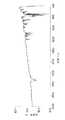
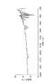
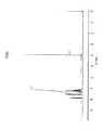
【0095】
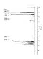
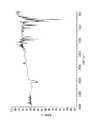
赤外吸収スペクトル:図2
NMRスペクトル: 図3
示差走査熱量測定(DSC):融点450℃、ガラス転移温度181℃
【0096】
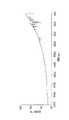
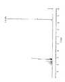
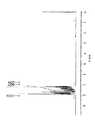
<実施例2>
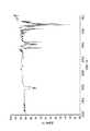
化合物II−1の合成
ビス(1,5−シクロオクタジエン)ニッケル(Ni(cod)2 )0.37g (1.35mmol)、2,2’−ビピリジン0.20g (1.28mmol)と、1,5−シクロオクタジエン0.20mlを、N,N−ジメチルホルムアミド20mlに窒素雰囲気中で混合し、さらに1−クロロ−9,10−ジフェニルアントラセン1.00g (2.74mmol)を加え、60℃で24時間攪拌した。この反応溶液を1N塩酸水溶液に投入し、トルエンとクロロホルムで抽出し、水洗後、硫酸マグネシウムで乾燥した。得られた生成物をアセトンで再沈し、クロロホルムより3回再結晶し、トルエンを抽出溶媒としてシリカカラム精製し、0.20g の黄白色固体を得た。
【0097】
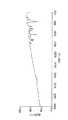
赤外吸収スペクトル:図4
NMRスペクトル: 図5
【0098】
<実施例3>
化合物 III−1の合成
シュレンクフラスコにアルゴン下で活性化したマグネシウム0.267g (10mmol)に、4,4’−ジ−ヨードビフェニル2.22g (5.46mmol)のテトラヒドロフラン(THF)溶液50mlを滴下しグリニャール化した。この反応溶液にNiCl2 (dppe)0.4g と2−クロロ−9,10−ジフェニルアントラセン4.00g (10mmol)を加え、60℃で4時間還流した。この反応溶液を1N塩酸水溶液に投入しトルエンとクロロホルムで抽出し、水洗後、硫酸マグネシウムで乾燥した。溶媒を留去後、アセトン/ジクロロメタンにより再結晶し、さらにトルエンとヘキサンを抽出溶媒としてシリカカラム精製し、2.0g の青緑色蛍光を示す黄白色固体を得た。この黄白色固体1.0g を昇華精製し、0.6g の純粋な黄白色固体を得た。
【0099】
元素分析: C H
計算値/% 94.78 5.22
測定値/% 94.50 5.40
示差走査熱量測定(DSC):融点350℃、ガラス転移温度120℃
イオン化ポテンシャル:5.95eV
【0100】
なお、赤外吸収スペクトル、NMRスペクトルの結果からも、上記化合物と同定した。
【0101】
<実施例4>
化合物V−1の合成
シュレンクフラスコにアルゴン下で活性化したマグネシウム0.267g (10mmol)に、4,4’−ジ−ヨードビフェニル2.02g (4.97mmol)のTHF溶液50mlを滴下しグリニャール化した。この反応溶液をアントラキノン1.04g (5mmol)のTHF溶液中に滴下し1時間攪拌した。この後フェニルマグネシウムアイオダイドのTHF溶液を滴下し、60℃で2時間還流した。反応溶液を1N塩酸水溶液に投入しトルエンとクロロホルムで抽出し、水洗後、硫酸マグネシウムで乾燥した。次に、この生成物を酢酸100mlに溶解し沃化水素水溶液を滴下後4時間攪拌した。この溶液に二塩化スズ(SnCl2 )の塩酸溶液を遊離した沃素が消えるまで入れた。クロロホルムとトルエンで抽出し硫酸マグネシウムで乾燥した。溶媒を留去後、トルエンを溶出溶媒としてシリカカラム精製した後、アセトン/トルエンより再結晶した。
なお、赤外吸収スペクトル、NMRスペクトルの結果からも、上記化合物と同定した。
【0102】
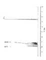
<実施例5>
化合物 VII−2の合成
シュレンクフラスコにアルゴン下で、ビアントロン1.0g (2.6mmol)をTHF50mlに溶解し、この溶液中に、4−メチルフェニルマグネシウムブロマイドのエーテル溶液(6.0mmol)を滴下し、4時間還流した。この反応溶液を、塩化アンモニウム水溶液に投入し、トルエンとクロロホルムで抽出し、水洗後、硫酸マグネシウムで乾燥した。次にこの生成物を酢酸100mlに溶解し、沃化水素水溶液を滴下後、4時間攪拌し、二塩化スズ(SnCl2 )の塩酸溶液を滴下し、さらに100℃で1時間攪拌した。この後、水を加え、クロロホルムとトルエンで抽出し、硫酸マグネシウムで乾燥した。溶媒を留去した後、アセトン、メタノールで洗浄し、トルエンとヘキサン(1:4)を溶出溶媒としてシリカカラム精製後、トルエンより再結晶し、0.8g の白色固体を得た。
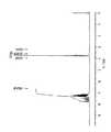
質量分析:m/e 535(M+1)+
赤外吸収スペクトル:図6
NMRスペクトル: 図7
示差走査熱量測定(DSC):融点365℃、ガラス転移温度162℃
【0103】
なお、元素分析における計算値と測定値もよく一致した。
【0104】
<実施例6>
化合物 VII−1の合成
実施例5に準じて合成した。
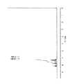
質量分析:m/e 506(M+ )
赤外吸収スペクトル:図8
NMRスペクトル: 図9
示差走査熱量測定(DSC):融点350℃、ガラス転移温度130℃
【0105】
なお、元素分析における計算値と測定値もよく一致した。
【0106】
<実施例7>
化合物 VII−3の合成
実施例5に準じて合成した。
質量分析:m/e 619(M+1)+
赤外吸収スペクトル:図10
NMRスペクトル: 図11
示差走査熱量測定(DSC):融点411℃
【0107】
なお、元素分析における計算値と測定値もよく一致した。
【0108】
<実施例8>
化合物 VII−4の合成
実施例5に準じて合成した。
赤外吸収スペクトル:図12
NMRスペクトル: 図13
【0109】
なお、元素分析における計算値と測定値もよく一致した。
【0110】
<実施例9>
化合物 VII−8の合成
実施例5に準じて合成した。
質量分析:m/e 658(M+ )
赤外吸収スペクトル:図14
NMRスペクトル: 図15
示差走査熱量測定(DSC):融点345℃、ガラス転移温度188℃
【0111】
なお、元素分析における計算値と測定値もよく一致した。
【0112】
<実施例10>
化合物 VII−12の合成
実施例5に準じて合成した。
質量分析:m/e 535(M+1)+
赤外吸収スペクトル:図16
NMRスペクトル: 図17
示差走査熱量測定(DSC):融点391℃、ガラス転移温度166℃
【0113】
なお、元素分析における計算値と測定値もよく一致した。
【0114】
<実施例11>
化合物 VII−14の合成
実施例5に準じて合成した。
質量分析:m/e 647(M+1)+
赤外吸収スペクトル:図18
NMRスペクトル: 図19
示差走査熱量測定(DSC):融点414℃で昇華
【0115】
なお、元素分析における計算値と測定値もよく一致した。
【0116】
<実施例12>
化合物 VII−15の合成
実施例5に準じて合成した。
質量分析:m/e 659(M+1)+
赤外吸収スペクトル:図20
NMRスペクトル: 図21
示差走査熱量測定(DSC):融点323℃、ガラス転移温度165℃
【0117】
なお、元素分析における計算値と測定値もよく一致した。
【0118】
<実施例13>
化合物 VII−16の合成
実施例5に準じて合成した。
質量分析:m/e 659(M+1)+
赤外吸収スペクトル:図22
NMRスペクトル: 図23
示差走査熱量測定(DSC):融点295℃、ガラス転移温度141℃
【0119】
なお、元素分析における計算値と測定値もよく一致した。
【0120】
<実施例14>
化合物 VII−24の合成
実施例5に準じて合成した。
質量分析:m/e 618(M+ )
赤外吸収スペクトル:図24
NMRスペクトル: 図25
示差走査熱量測定(DSC):融点273℃、ガラス転移温度105℃
【0121】
なお、元素分析における計算値と測定値もよく一致した。
【0122】
<実施例15>
化合物 VII−25の合成
実施例5に準じて合成した。
質量分析:m/e 567(M+1)+
赤外吸収スペクトル:図26
NMRスペクトル: 図27
【0123】
なお、元素分析における計算値と測定値もよく一致した。
【0124】
<実施例16>
化合物 VII−26の合成
実施例5に準じて合成した。
質量分析:m/e 606(M+ )
赤外吸収スペクトル:図28
NMRスペクトル: 図29
示差走査熱量測定(DSC):融点453℃、ガラス転移温度235℃
【0125】
なお、元素分析における計算値と測定値もよく一致した。
【0126】
<実施例17>
化合物 I−20の合成
実施例1に準じて合成した。
質量分析:m/e 883(M+1)+
赤外吸収スペクトル:図30
NMRスペクトル: 図31
示差走査熱量測定(DSC):融点342.6℃、ガラス転移温度103℃
【0127】
なお、元素分析における計算値と測定値もよく一致した。
【0128】
<実施例18>
化合物 VII−27の合成
実施例5に準じて合成した。
質量分析:m/e 896(M+ )
赤外吸収スペクトル:図32
NMRスペクトル: 図33
示差走査熱量測定(DSC):融点361.5℃、ガラス転移温度164℃
【0129】
なお、元素分析における計算値と測定値もよく一致した。
【0130】
<実施例19>
化合物 VII−23の合成
実施例5に準じて合成した。
赤外吸収スペクトル:図34
NMRスペクトル: 図35
示差走査熱量測定(DSC):融点423℃、ガラス転移温度190℃
【0131】
なお、元素分析における計算値と測定値もよく一致した。
【0132】
<実施例20>
化合物 I−17の合成
実施例1に準じて合成した。
赤外吸収スペクトル:図36
NMRスペクトル: 図37
示差走査熱量測定(DSC):ガラス転移温度177℃
【0133】
なお、元素分析における計算値と測定値もよく一致した。
【0134】
化6〜化24に示される他の例示化合物も実施例1〜20に準じて合成した。これらの化合物は、元素分析、赤外吸収スペクトル、NMRスペクトル、質量分析等の結果から同定した。
【0135】
<実施例21>
厚さ100nmのITO透明電極(陽極)を有するガラス基板を、中性洗剤、アセトン、エタノールを用いて超音波洗浄し、煮沸エタノール中から引き上げて乾燥し、蒸着装置の基板ホルダーに固定して、1×10⁻⁶Torrまで減圧した。
【0136】
次いで、N,N’−ジフェニル−N,N’−m−トリル−4,4’−ジアミノ−1,1’−ビフェニル(TPD−1)を蒸着速度0.2nm/secで50nmの厚さに蒸着し、正孔注入輸送層とした。
【0137】
次いで、実施例1の化合物I−1を蒸着速度0.2nm/secで50nmの厚さに蒸着し、発光層とした。
【0138】
次いで、減圧状態を保ったまま、電子注入輸送層として、トリス(8−キノリノラト)アルミニウムを蒸着速度0.2nm/secで10nmの厚さに蒸着した。
【0139】
さらに、減圧状態を保ったまま、MgAg(重量比10:1)を蒸着速度0.2nm/secで200nmの厚さに蒸着して陰極とし、有機EL素子を得た。
【0140】
この有機EL素子に電圧を印加して電流を流したところ、15V 、217mA/cm2で4500cd/m2 の青色(発光極大波長λmax =485nm)の発光が確認され、この発光は乾燥窒素雰囲気中で500時間以上安定していた。部分的非発光部の出現および成長は全くなかった。輝度の半減期は10mA/cm2の定電流駆動で100時間であった。
【0141】
<実施例22>
厚さ100nmのITO透明電極(陽極)を有するガラス基板を、中性洗剤、アセトン、エタノールを用いて超音波洗浄し、煮沸エタノール中から引き上げて乾燥し、蒸着装置の基板ホルダーに固定して、1×10⁻⁶Torrまで減圧した。
【0142】
次いで、ポリ(チオフェン−2,5−ジイル)を10nmの厚さに蒸着し、正孔注入層とした。
【0143】
次いで、N,N’−ジフェニル−N,N’−m−トリル−4,4’−ジアミノ−1,1’−ビフェニル(TPD−1)を蒸着速度0.2nm/secで50nmの厚さに蒸着し、正孔輸送層とした。
【0144】
次いで、実施例1の化合物I−1を50nmの厚さに蒸着し、発光層とした。
【0145】
次いで、減圧状態を保ったまま、電子注入輸送層として、トリス(8−キノリノラト)アルミニウムを蒸着速度0.2nm/secで10nmの厚さに蒸着した。
【0146】
さらに、減圧状態を保ったまま、MgAg(重量比10:1)を蒸着速度0.2nm/secで200nmの厚さに蒸着して陰極とし、有機EL素子を得た。
【0147】
この有機EL素子に電圧を印加して電流を流したところ、12V 、625mA/cm2で10000cd/m2 の青色(発光極大波長λmax =485nm)の発光が確認され、この発光は乾燥窒素雰囲気中で1000時間以上安定していた。部分的非発光部の出現および成長は全くなかった。輝度の半減期は10mA/cm2の定電流駆動で400時間であった。
【0148】
<実施例23>
実施例22において、電子注入輸送層を設けないほかは同様にして有機EL素子を得た。
【0149】
この有機EL素子に電圧を印加して電流を流したところ、12V 、825mA/cm2で2260cd/m2 の青色(発光極大波長λmax =485nm)の発光が確認され、この発光は乾燥窒素雰囲気中で500時間以上安定していた。部分的非発光部の出現および成長は全くなかった。輝度の半減期は10mA/cm2の定電流駆動で100時間であった。
【0150】
<実施例24>
実施例22と同様に素子を作製した。ただし、ホール輸送材料TPD−1の代わりに、N,N,N’,N’−テトラキス(3−ビフェニル)−4,4’−ジアミノ−1,1’−ビフェニル(TPD−2)を用いた。
【0151】
この有機EL素子に電圧を印加して電流を流したところ、12V 、675mA/cm2で5500cd/m2 の青色(発光極大波長λmax =485nm)の発光が確認され、この発光は乾燥窒素雰囲気中で1000時間以上安定していた。部分的非発光部の出現および成長は全くなかった。輝度の半減期は10mA/cm2の定電流駆動で600時間であった。
【0152】
<実施例25>
実施例24と同様に正孔輸送層を形成した後、次いで発光層として、TPD−2と実施例1の化合物I−1とを1:1の比率(重量比)で蒸着速度0.2nm/secで20nmの厚さに、共蒸着した。
【0153】
次いで、減圧状態を保ったまま、電子輸送層として、化合物I−1を50nmの厚さに蒸着した。
【0154】
次いで、減圧状態を保ったまま、電子注入層として、トリス(8−キノリノナト)アルミニウムを蒸着速度0.2nm/secで10nmの厚さに蒸着した。
【0155】
さらに、減圧状態を保ったまま、MgAg(重量比10:1)を蒸着速度0.2nm/secで200nmの厚さに蒸着して陰極とし、有機EL素子を得た。
【0156】
この素子に電圧を印加して電流を流したところ、12V 、540mA/cm2で12000cd/m2 の青色(発光極大波長λmax =480nm)の発光が確認された。この発光は乾燥窒素雰囲気中で5000時間以上安定していた。部分的非発光部の出現、成長および電流リークは全くなかった。輝度の半減期は10mA/cm2の定電流駆動で1500時間であった。
【0157】
<実施例26>
厚さ100nmのITO透明電極(陽極)を有するガラス基板を、中性洗剤、アセトン、エタノールを用いて超音波洗浄し、煮沸エタノール中から引き上げて乾燥し、蒸着装置の基板ホルダーに固定して、1×10⁻⁶Torrまで減圧した。
【0158】
次いで、ポリ(チオフェン−2,5−ジイル)を10nmの厚さに蒸着し、正孔注入層とした。
【0159】
次いで、N,N’−ジフェニル−N,N’−m−トリル−4,4’−ジアミノ−1,1’−ビフェニル(TPD−1)を蒸着速度0.2nm/secで50nmの厚さに蒸着し、正孔輸送層とした。
【0160】
次いで、実施例2の化合物II−1を50nmの厚さに蒸着し、発光層とした。
【0161】
次いで、減圧状態を保ったまま、電子注入輸送層として、トリス(8−キノリノラト)アルミニウムを蒸着速度0.2nm/secで10nmの厚さに蒸着した。
【0162】
さらに、減圧状態を保ったまま、MgAg(重量比10:1)を蒸着速度0.2nm/secで200nmの厚さに蒸着して陰極とし、有機EL素子を得た。
【0163】
この有機EL素子に電圧を印加して電流を流したところ、12V 、625mA/cm2で12000cd/m2 の青緑色(発光極大波長λmax =495nm)の発光が確認され、この発光は乾燥窒素雰囲気中で1000時間以上安定していた。部分的非発光部の出現および成長は全くなかった。輝度の半減期は10mA/cm2の定電流駆動で100時間であった。
【0164】
<実施例27>
実施例21において、化合物I−1のかわりに実施例5の化合物VII −2を用いて有機EL素子を得た。
【0165】
この素子に電圧を印加して電流を流したところ、14V 、450mA/cm2で1921cdm-2 の青色発光(発光極大波長λmax =460nm)の発光が確認され、この発光は乾燥窒素雰囲気中で1000時間以上安定していた。部分的非発光部の出現および成長は全くなかった。輝度の半減期は10mA/cm2の定電流駆動で300時間であった。
【0166】
<実施例28>
実施例22において、発光層を形成した後、トリス(8−キノリナト)アルミニウムを蒸着速度0.2nm/secで20nmの厚さに蒸着し、電子輸送層とした。次いで、テトラブチルジフェノキノンを10nmの厚さに蒸着し、電子注入層とした。その後、実施例22と同様にして有機EL素子を得た。
【0167】
この有機EL素子に実施例22と同様の条件で電圧を印加したところ、12V 、625mA/cm2で10000cd/m2 の青色(発光極大波長λmax =485nm)の発光が確認され、この発光は乾燥窒素雰囲気中で1000時間以上安定していた。部分的非発光部の出現および成長は全くなかった。輝度の半減期は10mA/cm2の定電流駆動で80時間であった。
【0168】
<実施例29>
厚さ100nmのITO透明電極(陽極)を有するガラス基板を、中性洗剤、アセトン、エタノールを用いて超音波洗浄し、煮沸エタノール中から引き上げて乾燥し、蒸着装置の基板ホルダーに固定して、1×10⁻⁶Torrまで減圧した。
【0169】
次いで、ポリ(チオフェン−2,5−ジイル)を10nmの厚さに蒸着し、正孔注入層とした。
【0170】
次いで、N,N’−ジフェニル−N,N’−m−トリル−4,4’−ジアミノ−1,1’−ビフェニル(TPD−1)を蒸着速度0.2nm/secで50nmの厚さに蒸着し、正孔輸送層とした。
【0171】
次いで、テトラフェニルシクロペンタジエンを50nmの厚さに蒸着し、発光層とした。
【0172】
次いで、減圧状態を保ったまま、電子注入輸送層として、実施例1の化合物I−1を蒸着速度0.2nm/secで10nmの厚さに蒸着した。
【0173】
さらに、減圧状態を保ったまま、MgAg(重量比10:1)を蒸着速度0.2nm/secで200nmの厚さに蒸着して陰極とし、有機EL素子を得た。
【0174】
この有機EL素子に電圧を印加して電流を流したところ、12V 、100mA/cm2で800cd/m2 の青色(発光極大波長λmax =460nm)の発光が確認され、この発光は乾燥窒素雰囲気中で100時間以上安定していた。部分的非発光部の出現および成長は全くなかった。輝度の半減期は10mA/cm2の定電流駆動で10時間であった。
【0175】
実施例21〜29において、化6〜化24に掲げた本発明の化合物の1種または2種以上を適宜選択して、上記実施例以外の組合せで、発光層や電子注入輸送層に用いたところ、有機EL素子の層構成等に応じて、上記実施例と同様の結果が得られた。
【0176】
<比較例1>
厚さ100nmのITO透明電極(陽極)を有するガラス基板を、中性洗剤、アセトン、エタノールを用いて超音波洗浄し、煮沸エタノール中から引き上げて乾燥し、蒸着装置の基板ホルダーに固定して、1×10⁻⁶Torrまで減圧した。
【0177】
次いで、N,N’ビス(m−メチルフェニル)−N,N’−ジフェニル−1,1’−ビフェニル−4,4’−ジアミン(TPD−1)を50nmの厚さに蒸着し、正孔注入輸送層とした。
【0178】
次いで、減圧状態を保ったまま、1,3−ビス(5−(4−t−ブチルフェニル)−1,3,4−オキサジアゾ−2−イル)ベンゼン(OXD−7)を蒸着速度0.2nm/secで50nmの厚さに蒸着して、発光層とした。
【0179】
次いで、減圧状態を保ったまま、電子注入輸送層としてトリス(8−キノリノナト)アルミニウムを蒸着速度0.2nm/secで10nmの厚さに蒸着した。
【0180】
さらに、減圧状態を保ったまま、MgAg(重量比10:1)を蒸着速度0.2nm/secで200nmの厚さに蒸着して陰極とし、EL素子を得た。
【0181】
このEL素子に電圧を印加して電流を流したところ、14V 、127mA/cm2で550cd/m2 の青色(発光極大波長λmax =480nm)の発光が確認され、この発光は乾燥窒素雰囲気中で10時間にて、部分的非発光部の出現および成長がみられ、20時間にて絶縁破壊を起こした。輝度の半減期は10mA/cm2の定電流駆動で20分であった。
【0182】
<比較例2>
C.Adachi et al., Appli. Phys. Lett.,56,799 (1990) に記載の9,10−ジフェニルアントラセンを発光層に用いて、この文献と同構成の有機EL素子を組み立てた。すなわち、比較例1において、電子注入輸送層を設けることなく、9,10−ジフェニルアントラセンを同様に50nmの厚さに蒸着して、電子注入輸送層を兼ねる発光層とした。
【0183】
このEL素子は、有機化合物層が結晶化しており、電気的にショートした状態で、電圧を印加したところ青色の発光はみられたものの絶縁破壊した。
【0184】
【発明の効果】
本発明のフェニルアントラセン誘導体は、結晶性が低く、アモルファス状態の良好な膜を形成することができるので、有機EL素子用化合物、特に青色発光材料や電子注入輸送材料として用いることができる。
実際、本発明のフェニルアントラセン誘導体を用いた本発明の有機EL素子は電流リークがなく、非発光部分(ダークスポット)の発生・成長がなく、膜中の結晶化が抑制されるので連続発光の信頼性の高い素子となる。特に発光層に用いた場合1万cd/m2 以上の高輝度の青色発光が可能となる。
【図面の簡単な説明】
【図1】本発明のEL素子の構成例を示す側面図である。
【図2】本発明の化合物の赤外吸収スペクトルを示すグラフである。
【図3】本発明の化合物のNMRスペクトルを示すグラフである。
【図4】本発明の化合物の赤外吸収スペクトルを示すグラフである。
【図5】本発明の化合物のNMRスペクトルを示すグラフである。
【図6】本発明の化合物の赤外吸収スペクトルを示すグラフである。
【図7】本発明の化合物のNMRスペクトルを示すグラフである。
【図8】本発明の化合物の赤外吸収スペクトルを示すグラフである。
【図9】本発明の化合物のNMRスペクトルを示すグラフである。
【図10】本発明の化合物の赤外吸収スペクトルを示すグラフである。
【図11】本発明の化合物のNMRスペクトルを示すグラフである。
【図12】本発明の化合物の赤外吸収スペクトルを示すグラフである。
【図13】本発明の化合物のNMRスペクトルを示すグラフである。
【図14】本発明の化合物の赤外吸収スペクトルを示すグラフである。
【図15】本発明の化合物のNMRスペクトルを示すグラフである。
【図16】本発明の化合物の赤外吸収スペクトルを示すグラフである。
【図17】本発明の化合物のNMRスペクトルを示すグラフである。
【図18】本発明の化合物の赤外吸収スペクトルを示すグラフである。
【図19】本発明の化合物のNMRスペクトルを示すグラフである。
【図20】本発明の化合物の赤外吸収スペクトルを示すグラフである。
【図21】本発明の化合物のNMRスペクトルを示すグラフである。
【図22】本発明の化合物の赤外吸収スペクトルを示すグラフである。
【図23】本発明の化合物のNMRスペクトルを示すグラフである。
【図24】本発明の化合物の赤外吸収スペクトルを示すグラフである。
【図25】本発明の化合物のNMRスペクトルを示すグラフである。
【図26】本発明の化合物の赤外吸収スペクトルを示すグラフである。
【図27】本発明の化合物のNMRスペクトルを示すグラフである。
【図28】本発明の化合物の赤外吸収スペクトルを示すグラフである。
【図29】本発明の化合物のNMRスペクトルを示すグラフである。
【図30】本発明の化合物の赤外吸収スペクトルを示すグラフである。
【図31】本発明の化合物のNMRスペクトルを示すグラフである。
【図32】本発明の化合物の赤外吸収スペクトルを示すグラフである。
【図33】本発明の化合物のNMRスペクトルを示すグラフである。
【図34】本発明の化合物の赤外吸収スペクトルを示すグラフである。
【図35】本発明の化合物のNMRスペクトルを示すグラフである。
【図36】本発明の化合物の赤外吸収スペクトルを示すグラフである。
【図37】本発明の化合物のNMRスペクトルを示すグラフである。
【符号の説明】
1 有機EL素子
2 基板
3 陽極
4 正孔注入輸送層
5 発光層
6 電子注入輸送層
7 陰極[0001]
[Industrial application fields]
The present invention relates to an organic EL (electroluminescence) device, and more particularly to a device that emits light by applying an electric field to a laminated thin film made of an organic compound.
[0002]
[Prior art]
An organic EL element has a configuration in which a thin film containing a fluorescent organic compound is sandwiched between a cathode and an anode, and excitons (excitons) are generated by injecting electrons and holes into the thin film and recombining them. It is an element that emits light by utilizing light emission (fluorescence / phosphorescence) when this exciton is deactivated.
[0003]
The characteristics of the organic EL element are 100 to 10,000 cd / m at a low voltage of about 10V.2 It is possible to emit surface light with a level of high brightness and to emit light from blue to red by selecting the type of fluorescent material.
[0004]
On the other hand, the problems of the organic EL element are that the light emission life is short, the storage durability and the reliability are low.
(1) Physical change of organic compounds
(Growth of crystal domains causes interface non-uniformity and causes deterioration of charge injection capability, short circuit, and dielectric breakdown of the device. In particular, when low molecular weight compounds having a molecular weight of 500 or less are used, the appearance and growth of crystal grains may occur. In addition, even if the interface of ITO or the like is rough, remarkable crystal grains appear and grow, resulting in a decrease in luminous efficiency, current leakage, and no light emission. (It also causes dark spots that are partially non-light emitting parts.)
[0005]
(2) Oxidation and peeling of cathode
(In order to facilitate the injection of electrons, Na, Mg, Al, etc. have been used as metals with small work functions. However, these metals react with moisture and oxygen in the atmosphere, and the organic layer and the cathode can be separated. In particular, when a film is formed by spin coating using a polymer compound, etc., residual solvents and decomposition products during the film formation promote the oxidation reaction of the electrode, resulting in partial peeling of the electrode. A non-light emitting part is generated.)
[0006]
(3) Low luminous efficiency and high heat generation
(Because current flows in the organic compound, the organic compound must be placed under a high electric field strength, and it cannot escape from the heat generation. Due to the heat, the element deteriorates due to melting, crystallization, thermal decomposition, etc.・ Destruction occurs.)
[0007]
(4) Photochemical and electrochemical changes in organic compound layers
Etc.
[0008]
In particular, with respect to blue light-emitting elements, there are few blue light-emitting materials that provide reliable and stable elements. In general, a blue light emitting material has high crystallinity. For example, although diphenylanthracene has a high fluorescence quantum yield, it has high crystallinity, and this compound can be used as a light-emitting material to provide a device with high brightness, high efficiency, and high reliability even when it is fabricated. [C. Adachi, et al., Appli. Phys. Lett., 56, 799 (1990)].
[0009]
[Problems to be solved by the invention]
An object of the present invention is to provide a novel phenylanthracene derivative as an optical / electronic functional material with little physical change, photochemical change, and electrochemical change, and with this phenylanthracene derivative, the reliability and luminous efficiency are high. An organic EL element having various emission colors, in particular, a blue emission color is realized. In particular, using an organic thin film formed by vapor deposition of a compound with a large molecular weight, high reliability with reduced drive voltage and reduced brightness, current leakage, and the appearance / growth of non-light emitting parts during device operation It is to realize a high-luminance light emitting element.
[0010]
[Means for Solving the Problems]
Such purposes are as follows (1) to (5).
(1) The followingIn chemical 3 or chemical 4An organic EL device having at least one organic compound layer made of a thin film containing a phenylanthracene derivative.
[0011]
[Chemical Formula 3]
[Formula 4]
[In
In
(2) The above organic compound layer is a light emitting layer(1)Organic EL element.
(3) Further, the above (having at least one hole injection layer, at least one hole transport layer, and at least one electron injection transport layer)2) Organic EL device.
(4) The above further comprising at least one hole injection layer, at least one hole transport layer, at least one electron transport layer, and at least one electron injection layer.2) Organic EL device.
(5) The above organic compound layer is an electron injecting and transporting layer, and further has a light emitting layer(1)Organic EL element.
[0014]
[Action]
The organic EL device of the present invention uses the compound represented by the above formula (I), preferably the above
[0015]
Since the vapor-deposited film of the above compound is in a stable amorphous state, the thin film has excellent physical properties and uniform light emission is possible. In addition, it is stable for over a year in the atmosphere and does not cause crystallization.
[0016]
In addition, a stable amorphous thin film can be formed by spin coating with a chloroform solution.
[0017]
The organic EL device of the present invention emits light efficiently at a low driving voltage.
[0018]
In addition, the light emission maximum wavelength of the organic EL element of this invention is about 400-700 nm.
[0019]
[Specific configuration]
Hereinafter, a specific configuration of the present invention will be described in detail.
[0020]
The phenylanthracene derivative of the present invention is represented by the formula (I). When formula (I) is described, A1 And A2 Each represents a monophenylanthryl group or a diphenylanthryl group, which may be the same or different.
[0021]
A1 , A2 The monophenylanthryl group or diphenylanthryl group represented by the formula may be unsubstituted or have a substituent, and in the case of having a substituent, the substituent may be an alkyl group, an aryl group, an alkoxy group, An aryloxy group, an amino group, etc. are mentioned, and these substituents may be further substituted. These substituents will be described later. The substitution position of such a substituent is not particularly limited, but is preferably not a anthracene ring but a phenyl group bonded to the anthracene ring.
[0022]
Moreover, it is preferable that the bonding position of the phenyl group in the anthracene ring is the 9th or 10th position of the anthracene ring.
[0023]
In the formula (I), L represents a single bond or a divalent group, and the divalent group represented by L is preferably an arylene group in which an alkylene group or the like may be interposed. Such an arylene group will be described later.
[0024]
Among the phenylanthracene derivatives represented by the formula (I), those represented by
[0025]
R1 , R2 The alkyl group represented by may be linear or branched, and is preferably a substituted or unsubstituted alkyl group having 1 to 10 carbon atoms and more preferably 1 to 4 carbon atoms. In particular, an unsubstituted alkyl group having 1 to 4 carbon atoms is preferable, and specifically, a methyl group, an ethyl group, a (n-, i-) propyl group, (n-, i-, s-, t-) butyl. Groups and the like.
[0026]
R1 , R2 Examples of the cycloalkyl group represented by the formula include a cyclohexyl group and a cyclopentyl group.
[0027]
R1 , R2 As the aryl group represented by the formula, those having 6 to 20 carbon atoms are preferable, and further, those having a substituent such as a phenyl group and a tolyl group may be used. Specific examples include a phenyl group, (o-, m-, p-) tolyl group, pyrenyl group, naphthyl group, anthryl group, biphenyl group, phenylanthryl group, and tolylanthryl group.
[0028]
R1 , R2 As the alkenyl group represented by the formula, those having a total carbon number of 6 to 50 are preferable, which may be unsubstituted, may have a substituent, and preferably have a substituent. In this case, the substituent is preferably an aryl group such as a phenyl group. Specific examples include a triphenyl vinyl group, a tolyl vinyl group, and a tribiphenyl vinyl group.
[0029]
R1 , R2 As the alkoxy group represented by formula (1), an alkyl group having 1 to 6 carbon atoms is preferable, and specific examples include a methoxy group and an ethoxy group. The alkoxy group may be further substituted.
[0030]
R1 , R2 Examples of the aryloxy group represented by the formula include a phenoxy group.
[0031]
R1 , R2 The amino group represented by may be unsubstituted or have a substituent, but preferably has a substituent. In this case, examples of the substituent include an alkyl group (methyl group, ethyl group, etc.), aryl Group (phenyl group etc.) etc. are mentioned. Specific examples include a diethylamino group, a diphenylamino group, and a di (m-tolyl) amino group.
[0032]
R1 , R2 Examples of the heterocyclic group represented by the formula include bipyridyl group, pyrimidyl group, quinolyl group, pyridyl group, thienyl group, furyl group, oxadiazoyl group and the like. These may have a substituent such as a methyl group or a phenyl group.
[0033]
In
[0034]
In
[0035]
In
[0036]
L1 The arylene group represented by may be a group in which two or more arylene groups are linked via an alkylene group, —O—, —S— or —NR—. Here, R represents an alkyl group or an aryl group. Examples of the alkyl group include a methyl group and an ethyl group, and examples of the aryl group include a phenyl group. Among them, an aryl group is preferable, and in addition to the above phenyl group, A1 , A2 Furthermore, A may be added to the phenyl group.1 Or A2 May be substituted.
[0037]
The alkylene group is preferably a methylene group or an ethylene group. Specific examples of such an arylene group are shown below.
[0038]
[Chemical formula 5]
Next, the
[0040]
In
[0041]
Although the compound represented by
[0042]
[Chemical 6]
[Chemical 7]
[Chemical 8]
[Chemical 9]
[Chemical Formula 10]
Embedded image
Embedded image
Embedded image
Embedded image
Embedded image
Embedded image
Embedded image
Embedded image
Embedded image
Embedded image
Embedded image
Embedded image
Embedded image
Embedded image
The phenylanthracene derivative of the present invention (hereinafter also referred to as “the compound of the present invention”)
(1) Halogenated diphenylanthracene compound is converted to Ni (cod)2 Coupling with [cod: 1,5-cyclooctadiene] or Grignard aryl dihalide to form NiCl2 (Dppe) [dppe: diphenylphosphinoethane], NiCl2 (Dppp) [dppp: diphenylphosphinopropane], a method of cross-coupling using a Ni complex or the like,
(2) a method of cross-coupling by reaction and reduction of anthraquinone, benzoquinone, phenylanthrone or bianthrone with a Grignard aryl or lithiated aryl,
Etc.
[0062]
The compound thus obtained is elemental analysis, mass spectrometry, infrared absorption spectrum,1H or13C nuclear magnetic resonance absorption (NMR) spectra can be identified.
[0063]
The phenylanthracene derivative of the present invention has a molecular weight of about 400 to 2000, more preferably about 400 to 1000, a high melting point of 200 to 500 ° C., 80 to 250 ° C., further 100 to 250 ° C., and more It exhibits a glass transition temperature (Tg) of 130 to 250 ° C., particularly 150 to 250 ° C. Accordingly, a smooth and good film in an amorphous state that is transparent and stable even at room temperature or higher is formed by ordinary vacuum deposition or the like, and the good film state is maintained for a long period of time.
[0064]
The organic EL device of the present invention (hereinafter also referred to as “EL device”) has at least one organic compound layer, and at least one organic compound layer contains the compound of the present invention. A configuration example of the organic EL element of the present invention is shown in FIG. The
[0065]
The light emitting layer has a hole and electron injection function, a transport function thereof, and a function of generating excitons by recombination of holes and electrons. The hole injecting and transporting layer has the function of facilitating the injection of holes from the anode, the function of transporting holes and the function of hindering the transport of electrons, and the electron injecting and transporting layer prevents the injection of electrons from the cathode. It has a function to facilitate, a function to transport electrons, and a function to prevent the transport of holes, and these layers increase and confine holes and electrons injected into the light-emitting layer and optimize the recombination region. To improve luminous efficiency. The electron injecting and transporting layer and the hole injecting and transporting layer are provided as necessary in consideration of the height of each function of electron injection, electron transport, hole injection and hole transport of the compound used for the light emitting layer. For example, when the hole injection / transport function or electron injection / transport function of the compound used in the light-emitting layer is high, the light-emitting layer is not provided with the hole injection / transport layer or the electron injection / transport layer, but the hole injection / transport layer or the electron injection It can be set as the structure which serves as a transport layer. In some cases, neither the hole injection transport layer nor the electron injection transport layer may be provided. Further, each of the hole injecting and transporting layer and the electron injecting and transporting layer may be provided with a layer having an injection function and a layer having a transport function.
[0066]
Since the compound of the present invention is a relatively neutral compound, it is preferably used in the light emitting layer, but can also be applied to a hole injecting and transporting layer and an electron injecting and transporting layer.
[0067]
In addition, the recombination region and light emission can be controlled by controlling the film thickness while considering the carrier mobility and carrier density (determined by the ionization potential and electron affinity) of the light-emitting layer, electron injection transport layer, and hole injection transport layer to be combined. The region can be designed freely, and it is possible to design the light emission color, control the light emission luminance / light emission spectrum by the interference effect of both electrodes, and control the spatial distribution of light emission.
[0068]
The case where the compound of the present invention is used for the light emitting layer will be described. In addition to the compound of the present invention, other fluorescent materials may be used for the light-emitting layer. Examples of other fluorescent materials include compounds disclosed in JP-A-63-264692, for example, And at least one selected from compounds such as quinacridone, rubrene, and styryl dyes. The content of such a fluorescent substance is preferably 10 mol% or less of the compound of the present invention. By appropriately selecting and adding such a compound, emitted light can be shifted to the long wavelength side.
[0069]
The light emitting layer may contain a singlet oxygen quencher. Examples of such quenchers include nickel complexes, rubrene, diphenylisobenzofuran, and tertiary amines. The content of such a quencher is preferably 10 mol% or less of the compound of the present invention.
[0070]
When the compound of the present invention is used for the light emitting layer, the hole injection transport layer and the electron injection transport layer include various organic compounds used in ordinary organic EL devices, for example, JP-A 63-295695. Various organic compounds described in, for example, Kaihei 2-191694 and JP-A-3-792 can be used. For example, an aromatic tertiary amine, a hydrazone derivative, a carbazole derivative, a triazole derivative, an imidazole derivative, or the like can be used for the hole injecting and transporting layer, and an organometallic complex such as aluminum quinolinol is used for the electron injecting and transporting layer. Derivatives, oxadiazole derivatives, pyridine derivatives, pyrimidine derivatives, quinoline derivatives, quinoxaline derivatives, diphenylquinone derivatives, perylene derivatives, fluorene derivatives, and the like can be used.
[0071]
When the hole injecting and transporting layer is divided into a hole injecting layer and a hole transporting layer, a preferred combination can be selected from the compounds for the hole injecting and transporting layer. At this time, it is preferable to laminate in order of a compound layer having a small ionization potential from the anode (ITO or the like) side. Further, it is preferable to use a compound having a good thin film property on the anode surface. Such a stacking order is the same when two or more hole injection / transport layers are provided. By adopting such a stacking order, the drive voltage is lowered, and the occurrence of current leakage and the generation / growth of dark spots can be prevented. In addition, in the case of forming an element, since vapor deposition is used, a thin film of about 1 to 10 nm can be made uniform and pinhole-free, so that the ion injection potential is small in the hole injection layer and the visible portion has absorption. Even if such a compound is used, it is possible to prevent a decrease in efficiency due to a change in color tone of light emission or reabsorption.
[0072]
When the electron injecting and transporting layer is divided into an electron injecting layer and an electron transporting layer, a preferred combination can be selected from the compounds for the electron injecting and transporting layer. At this time, it is preferable to laminate in the order of the layer of the compound having a large electron affinity value from the cathode side. Such a stacking order is the same when two or more electron injecting and transporting layers are provided.
[0073]
In the present invention, the light emitting layer is preferably a mixed layer of an electron injecting and transporting compound and a hole injecting and transporting compound. And the compound of this invention is contained in such a mixed layer. Since the compound of the present invention is usually contained as a fluorescent substance, more specifically, when the compound of the present invention is an electron injection / transport compound, another hole injection / transport compound is further added. When the compound of the present invention is a hole injecting / transporting compound, it is preferable to further add another electron injecting / transporting compound. The mixing ratio of the electron injecting and transporting compound and the hole injecting and transporting compound in the mixed layer is a weight ratio, and the ratio of the electron injecting and transporting compound to the hole injecting and transporting compound is 60:40 to 40:60. Is particularly preferable, and it is preferably about 50:50.
[0074]
The electron injecting and transporting compound to be used for the mixing is selected from the above compounds for the electron injecting and transporting layer, and the hole injecting and transporting compound is selected from the above compounds for the hole injecting and transporting layer. be able to. In some cases, the compounds of the present invention may be selected and used. Furthermore, in the mixed layer, each of the electron injecting and transporting compound and the hole injecting and transporting compound may be used alone or in combination of two or more. The mixed layer may be doped with the compound of the present invention or another fluorescent substance in order to increase the emission intensity.
[0075]
Furthermore, a mixed layer of another electron injecting and transporting compound and another hole injecting and transporting compound may be used, and such a mixed layer may be doped with the compound of the present invention.
[0076]
By applying such a mixed layer to an EL element, the stability of the element is improved.
[0077]
The compound of the present invention is also preferably used for an electron injecting and transporting layer. In this case, the fluorescent substance used for the light emitting layer is preferably a substance having fluorescence having a wavelength longer than or comparable to that of the compound of the present invention. For example, the fluorescent material that can be used in combination with the compound of the present invention in the light emitting layer can be selected and used. Moreover, the compound of this invention can be used also for a light emitting layer in such a structure. Moreover, the compound of this invention can be used also for the light emitting layer which served as the electron injection transport layer.
[0078]
The compound of this invention can be used for a positive hole injection transport layer.
[0079]
When the compound of the present invention is used for the hole injecting and transporting layer, the fluorescent substance used for the light emitting layer may be selected from those having longer wavelength fluorescence than the compound of the present invention. What is necessary is just to select suitably from 1 or more types of the fluorescent substance used together with the compound of invention. In such a case, the compound of this invention can be used also for a light emitting layer.
[0080]
In addition, in the above, when using another fluorescent substance mainly for a light emitting layer, you may add and use the compound of this
[0081]
The thickness of the light-emitting layer, the thickness of the hole injecting and transporting layer, and the thickness of the electron injecting and transporting layer are not particularly limited, and may vary depending on the formation method, but is usually about 5 to 1000 nm, particularly 8 to 200 nm. preferable.
[0082]
The thickness of the hole injecting and transporting layer and the thickness of the electron injecting and transporting layer may be about the same as the thickness of the light emitting layer or about 1/10 to 10 times depending on the design of the recombination / light emitting region. When the injection layer and the transport layer for electrons or holes are separated, the injection layer is preferably 1 nm or more, and the transport layer is preferably 20 nm or more. In this case, the upper limit of the thickness of the injection layer and the transport layer is usually about 100 nm for the injection layer and about 1000 nm for the transport layer.
[0083]
For the cathode, it is preferable to use a material having a low work function, such as Li, Na, Mg, Al, Ag, In, or an alloy containing one or more of these materials. Further, the cathode preferably has fine crystal grains, and particularly preferably in an amorphous state. The thickness of the cathode is preferably about 10 to 1000 nm.
[0084]
In order to cause the EL element to emit light, at least one of the electrodes needs to be transparent or translucent, and as described above, the cathode material is limited, so that the transmittance of emitted light is preferably 80% or more. It is preferable to determine the material and thickness of the anode so that Specifically, for example, ITO, SnO2 Ni, Au, Pt, Pd, polypyrrole doped with a dopant, or the like is preferably used for the anode. The thickness of the anode is preferably about 10 to 500 nm. In order to improve the reliability of the element, the drive voltage needs to be low, but a preferable one is about 10 to 30 Ω / □ and ITO of 10 Ω / □ or less (usually 5 to 10 Ω / □) is mentioned. .
[0085]
The substrate material is not particularly limited, but in the illustrated example, a transparent or translucent material such as glass or resin is used to extract emitted light from the substrate side. Further, the emission color may be controlled by using a color filter film or a dielectric reflection film on the substrate.
[0086]
Note that when an opaque material is used for the substrate, the stacking order shown in FIG. 1 may be reversed.
[0087]
Next, the manufacturing method of the organic EL element of this invention is demonstrated.
[0088]
The cathode and the anode are preferably formed by vapor deposition such as vapor deposition or sputtering.
[0089]
For the formation of the hole injecting and transporting layer, the light emitting layer, and the electron injecting and transporting layer, it is preferable to use a vacuum deposition method because a homogeneous thin film can be formed. When the vacuum deposition method is used, a homogeneous thin film having an amorphous state or a crystal grain size of 0.1 μm or less (usually 0.01 μm or more) can be obtained. If the crystal grain size exceeds 0.1 μm, non-uniform light emission occurs, the drive voltage of the device must be increased, and the charge injection efficiency is also significantly reduced.
[0090]
The conditions for vacuum deposition are not particularly limited, but 10-FiveThe degree of vacuum is less than Torr, and the deposition rate is preferably about 0.1 to 1 nm / sec. Moreover, it is preferable to form each layer continuously in a vacuum. If formed continuously in a vacuum, impurities can be prevented from adsorbing to the interface of each layer, so that high characteristics can be obtained. In addition, the driving voltage of the element can be lowered.
[0091]
In the case of using a vacuum deposition method for forming each of these layers, when a plurality of compounds are contained in one layer, the temperature of each boat containing the compounds is individually controlled and co-deposited while being monitored with a crystal oscillator thickness meter. It is preferable.
[0092]
The EL element of the present invention is usually used as a direct current drive type EL element, but can be alternating current driven or pulse driven. The applied voltage is usually about 2 to 20V.
[0093]
【Example】
Hereinafter, specific examples of the present invention will be shown together with comparative examples, and the present invention will be described in more detail.
[0094]
<Example 1>
Synthesis of Compound I-1
Bis (1,5-cyclooctadiene) nickel (Ni (cod)2 ) 0.37 g (1.35 mmol), 2,2′-bipyridine 0.20 g (1.28 mmol) and 1,5-cyclooctadiene 0.20 ml in N, N-dimethylformamide 20 ml in a nitrogen atmosphere The mixture was further mixed, 1.00 g (2.74 mmol) of 2-chloro-9,10-diphenylanthracene was added, and the mixture was stirred at 60 ° C. for 24 hours. This reaction solution was poured into a 1N aqueous hydrochloric acid solution, extracted with toluene and chloroform, washed with water, and dried over magnesium sulfate. The obtained product was reprecipitated with acetone, recrystallized three times from chloroform, and purified on a silica column using toluene as an extraction solvent to obtain 0.53 g of a yellowish white solid. 0.5 g of the obtained yellowish white solid was purified by sublimation to obtain 0.23 g of a yellowish white solid having blue fluorescence.
[0095]
Infrared absorption spectrum: Fig. 2
NMR spectrum: FIG.
Differential scanning calorimetry (DSC): melting point 450 ° C., glass transition temperature 181 ° C.
[0096]
<Example 2>
CompoundIISynthesis of -1
Bis (1,5-cyclooctadiene) nickel (Ni (cod)2 ) 0.37 g (1.35 mmol), 2,2′-bipyridine 0.20 g (1.28 mmol) and 1,5-cyclooctadiene 0.20 ml in N, N-dimethylformamide 20 ml in a nitrogen atmosphere After mixing, 1.00 g (2.74 mmol) of 1-chloro-9,10-diphenylanthracene was added, and the mixture was stirred at 60 ° C. for 24 hours. This reaction solution was poured into a 1N aqueous hydrochloric acid solution, extracted with toluene and chloroform, washed with water, and dried over magnesium sulfate. The obtained product was reprecipitated with acetone, recrystallized three times from chloroform, and purified on a silica column using toluene as an extraction solvent to obtain 0.20 g of a yellowish white solid.
[0097]
Infrared absorption spectrum: Fig. 4
NMR spectrum: FIG.
[0098]
<Example 3>
CompoundIIISynthesis of -1
To 0.267 g (10 mmol) of magnesium activated under argon in a Schlenk flask, 50 ml of a tetrahydrofuran (THF) solution of 2.22 g (5.46 mmol) of 4,4'-di-iodobiphenyl was added dropwise to form a Grignard. NiCl is added to the reaction solution.2 0.4 g of (dppe) and 4.00 g (10 mmol) of 2-chloro-9,10-diphenylanthracene were added, and the mixture was refluxed at 60 ° C. for 4 hours. This reaction solution was poured into a 1N aqueous hydrochloric acid solution, extracted with toluene and chloroform, washed with water, and dried over magnesium sulfate. After distilling off the solvent, it was recrystallized from acetone / dichloromethane, and further purified with a silica column using toluene and hexane as extraction solvents to obtain 2.0 g of a yellowish white solid exhibiting blue-green fluorescence. Sublimation purification of 1.0 g of this yellowish white solid yielded 0.6 g of pure yellowish white solid.
[0099]
Elemental analysis: C H
Calculated value /% 94.78 5.22
Measurement /% 94.50 5.40
IndicationDifferential scanning calorimetry (DSC): melting point 350 ° C., glass transition temperature 120 ° C.
Ionization potential: 5.95 eV
[0100]
In addition, it identified as the said compound also from the result of the infrared absorption spectrum and the NMR spectrum.
[0101]
<Example 4>
Synthesis of Compound V-1
To 0.267 g (10 mmol) of magnesium activated under argon in a Schlenk flask, 50 ml of a THF solution of 2.02 g (4.97 mmol) of 4,4'-di-iodobiphenyl was added dropwise to form a Grignard. This reaction solution was dropped into a THF solution of 1.04 g (5 mmol) of anthraquinone and stirred for 1 hour. Thereafter, a THF solution of phenylmagnesium iodide was dropped, and the mixture was refluxed at 60 ° C. for 2 hours. The reaction solution was poured into a 1N aqueous hydrochloric acid solution, extracted with toluene and chloroform, washed with water, and dried over magnesium sulfate. Next, this product was dissolved in 100 ml of acetic acid, and an aqueous hydrogen iodide solution was added dropwise, followed by stirring for 4 hours. To this solution was added tin dichloride (SnCl2 ) Was added until the free iodine disappeared. Extraction with chloroform and toluene was followed by drying over magnesium sulfate. After distilling off the solvent, the silica column was purified using toluene as an elution solvent, and then recrystallized from acetone / toluene.
In addition, it identified as the said compound also from the result of the infrared absorption spectrum and the NMR spectrum.
[0102]
<Example 5>
CompoundVII-2 synthesis
Under argon, 1.0 g (2.6 mmol) of biantron was dissolved in 50 ml of THF under argon, and an ether solution (6.0 mmol) of 4-methylphenylmagnesium bromide was dropped into this solution and refluxed for 4 hours. . This reaction solution was poured into an aqueous ammonium chloride solution, extracted with toluene and chloroform, washed with water, and dried over magnesium sulfate. Next, this product was dissolved in 100 ml of acetic acid, and an aqueous hydrogen iodide solution was added dropwise, followed by stirring for 4 hours, and tin dichloride (SnCl2 ) Was added dropwise, and the mixture was further stirred at 100 ° C. for 1 hour. After this, water was added, extracted with chloroform and toluene, and dried over magnesium sulfate. After the solvent was distilled off, the residue was washed with acetone and methanol, purified with a silica column using toluene and hexane (1: 4) as an elution solvent, and recrystallized from toluene to obtain 0.8 g of a white solid.
Mass spectrometry: m / e 535 (M + 1)+
Infrared absorption spectrum: FIG.
NMR spectrum: FIG.
Differential scanning calorimetry (DSC): melting point 365 ° C., glass transition temperature 162 ° C.
[0103]
The calculated values and the measured values in elemental analysis were in good agreement.
[0104]
<Example 6>
CompoundVIISynthesis of -1
Synthesized according to Example 5.
Mass spectrometry: m / e 506 (M+ )
Infrared absorption spectrum: FIG.
NMR spectrum: FIG.
Differential scanning calorimetry (DSC): melting point 350 ° C., glass transition temperature 130 ° C.
[0105]
The calculated values and the measured values in elemental analysis were in good agreement.
[0106]
<Example 7>
CompoundVIISynthesis of -3
Synthesized according to Example 5.
Mass spectrometry: m / e 619 (M + 1)+
Infrared absorption spectrum: FIG.
NMR spectrum: FIG.
Differential scanning calorimetry (DSC): melting point 411 ° C.
[0107]
The calculated values and the measured values in elemental analysis were in good agreement.
[0108]
<Example 8>
Synthesis of Compound VII-4
Synthesized according to Example 5.
RedExternal absorption spectrum: FIG.
NMR spectrum: FIG.
[0109]
The calculated values and the measured values in elemental analysis were in good agreement.
[0110]
<Example 9>
CompoundVIISynthesis of -8
Synthesized according to Example 5.
Mass spectrometry: m / e 658 (M+ )
Infrared absorption spectrum: FIG.
NMR spectrum: FIG.
Differential scanning calorimetry (DSC): melting point 345 ° C., glass transition temperature 188 ° C.
[0111]
The calculated values and the measured values in elemental analysis were in good agreement.
[0112]
<Example 10>
CompoundVIISynthesis of -12
Synthesized according to Example 5.
Mass spectrometry: m / e 535 (M + 1)+
Infrared absorption spectrum: FIG.
NMR spectrum: FIG.
Differential scanning calorimetry (DSC): melting point 391 ° C., glass transition temperature 166 ° C.
[0113]
The calculated values and the measured values in elemental analysis were in good agreement.
[0114]
<Example 11>
CompoundVIISynthesis of -14
Synthesized according to Example 5.
Mass spectrometry: m / e 647 (M + 1)+
Infrared absorption spectrum: FIG.
NMR spectrum: FIG.
Differential scanning calorimetry (DSC): Sublimation at melting point 414 ° C
[0115]
The calculated values and the measured values in elemental analysis were in good agreement.
[0116]
<Example 12>
CompoundVIISynthesis of -15
Synthesized according to Example 5.
Mass spectrometry: m / e 659 (M + 1)+
Infrared absorption spectrum: FIG.
NMR spectrum: FIG.
Differential scanning calorimetry (DSC): melting point 323 ° C., glass transition temperature 165 ° C.
[0117]
The calculated values and the measured values in elemental analysis were in good agreement.
[0118]
<Example 13>
CompoundVIISynthesis of -16
Synthesized according to Example 5.
Mass spectrometry: m / e 659 (M + 1)+
Infrared absorption spectrum: FIG.
NMR spectrum: FIG.
Differential scanning calorimetry (DSC): melting point 295 ° C., glass transition temperature 141 ° C.
[0119]
The calculated values and the measured values in elemental analysis were in good agreement.
[0120]
<Example 14>
CompoundVIISynthesis of -24
Synthesized according to Example 5.
Mass spectrometry: m / e 618 (M+ )
Infrared absorption spectrum: FIG.
NMR spectrum: FIG.
Differential scanning calorimetry (DSC): melting point 273 ° C.,
[0121]
The calculated values and the measured values in elemental analysis were in good agreement.
[0122]
<Example 15>
CompoundVIISynthesis of -25
Synthesized according to Example 5.
Mass spectrometry: m / e 567 (M + 1)+
Infrared absorption spectrum: FIG.
NMR spectrum: FIG.
[0123]
The calculated values and the measured values in elemental analysis were in good agreement.
[0124]
<Example 16>
CompoundVII-26 synthesis
Synthesized according to Example 5.
Mass spectrometry: m / e 606 (M+ )
Infrared absorption spectrum: FIG.
NMR spectrum: FIG.
Differential scanning calorimetry (DSC): melting point 453 ° C., glass transition temperature 235 ° C.
[0125]
The calculated values and the measured values in elemental analysis were in good agreement.
[0126]
<Example 17>
CompoundISynthesis of -20
Synthesized according to Example 1.
Mass spectrometry: m / e 883 (M + 1)+
Infrared absorption spectrum: FIG.
NMR spectrum: FIG.
Differential scanning calorimetry (DSC): melting point 342.6 ° C., glass transition temperature 103 ° C.
[0127]
The calculated values and the measured values in elemental analysis were in good agreement.
[0128]
<Example 18>
CompoundVII-27 synthesis
Synthesized according to Example 5.
Mass spectrometry: m / e 896 (M+ )
Infrared absorption spectrum: FIG. 32
NMR spectrum: FIG.
Differential scanning calorimetry (DSC): melting point 361.5 ° C., glass transition temperature 164 ° C.
[0129]
The calculated values and the measured values in elemental analysis were in good agreement.
[0130]
<Example 19>
CompoundVIISynthesis of -23
Synthesized according to Example 5.
Infrared absorption spectrum: FIG.
NMR spectrum: FIG.
Differential scanning calorimetry (DSC): melting point 423 ° C., glass transition temperature 190 ° C.
[0131]
The calculated values and the measured values in elemental analysis were in good agreement.
[0132]
<Example 20>
CompoundISynthesis of -17
Synthesized according to Example 1.
Infrared absorption spectrum: FIG.
NMR spectrum: FIG.
Differential scanning calorimetry (DSC): Glass transition temperature 177 ° C
[0133]
The calculated values and the measured values in elemental analysis were in good agreement.
[0134]
Other exemplary compounds shown in
[0135]
<Example 21>
A glass substrate having an ITO transparent electrode (anode) with a thickness of 100 nm is ultrasonically cleaned with a neutral detergent, acetone, and ethanol, dried by boiling out from boiling ethanol, and fixed to a substrate holder of a vapor deposition apparatus. 1 × 10⁻⁶The pressure was reduced to Torr.
[0136]
Next, N, N′-diphenyl-N, N′-m-tolyl-4,4′-diamino-1,1′-biphenyl (TPD-1) was deposited to a thickness of 50 nm at a deposition rate of 0.2 nm / sec. It vapor-deposited and it was set as the positive hole injection transport layer.
[0137]
Subsequently, the compound I-1 of Example 1 was vapor-deposited in the thickness of 50 nm with the vapor deposition rate of 0.2 nm / sec, and it was set as the light emitting layer.
[0138]
Next, while maintaining the reduced pressure state, tris (8-quinolinolato) aluminum was deposited as an electron injecting and transporting layer to a thickness of 10 nm at a deposition rate of 0.2 nm / sec.
[0139]
Further, while maintaining the reduced pressure state, MgAg (weight ratio 10: 1) was vapor-deposited at a vapor deposition rate of 0.2 nm / sec to a thickness of 200 nm to obtain a cathode to obtain an organic EL device.
[0140]
When a voltage was applied to this organic EL element and a current was applied, 15 V, 217 mA / cm.24500cd / m2 Of blue light (maximum light emission wavelength λmax = 485 nm) was confirmed, and this light emission was stable for 500 hours or more in a dry nitrogen atmosphere. There was no emergence or growth of partially non-light emitting parts. Luminance half-life is 10mA / cm2The constant current driving was 100 hours.
[0141]
<Example 22>
A glass substrate having an ITO transparent electrode (anode) with a thickness of 100 nm is ultrasonically cleaned with a neutral detergent, acetone, and ethanol, dried by boiling out from boiling ethanol, and fixed to a substrate holder of a vapor deposition apparatus. 1 × 10⁻⁶The pressure was reduced to Torr.
[0142]
Next, poly (thiophene-2,5-diyl) was deposited to a thickness of 10 nm to form a hole injection layer.
[0143]
Next, N, N′-diphenyl-N, N′-m-tolyl-4,4′-diamino-1,1′-biphenyl (TPD-1) was deposited to a thickness of 50 nm at a deposition rate of 0.2 nm / sec. It vapor-deposited and it was set as the positive hole transport layer.
[0144]
Subsequently, the compound I-1 of Example 1 was vapor-deposited to a thickness of 50 nm to form a light emitting layer.
[0145]
Next, while maintaining the reduced pressure state, tris (8-quinolinolato) aluminum was deposited as an electron injecting and transporting layer to a thickness of 10 nm at a deposition rate of 0.2 nm / sec.
[0146]
Further, while maintaining the reduced pressure state, MgAg (weight ratio 10: 1) was vapor-deposited at a vapor deposition rate of 0.2 nm / sec to a thickness of 200 nm to obtain a cathode to obtain an organic EL device.
[0147]
When a voltage was applied to the organic EL element and a current was passed, 12 V, 625 mA / cm.210,000 cd / m2 Of blue light (maximum light emission wavelength λmax = 485 nm) was confirmed, and this light emission was stable for 1000 hours or more in a dry nitrogen atmosphere. There was no emergence or growth of partially non-light emitting parts. Luminance half-life is 10mA / cm2The constant current drive was 400 hours.
[0148]
<Example 23>
An organic EL device was obtained in the same manner as in Example 22 except that the electron injecting and transporting layer was not provided.
[0149]
When a voltage was applied to the organic EL element and a current was applied, 12 V, 825 mA / cm.22260cd / m2 Of blue light (maximum light emission wavelength λmax = 485 nm) was confirmed, and this light emission was stable for 500 hours or more in a dry nitrogen atmosphere. There was no emergence or growth of partially non-light emitting parts. Luminance half-life is 10mA / cm2The constant current driving was 100 hours.
[0150]
<Example 24>
A device was produced in the same manner as in Example 22. However, N, N, N ′, N′-tetrakis (3-biphenyl) -4,4′-diamino-1,1′-biphenyl (TPD-2) was used instead of the hole transport material TPD-1. .
[0151]
When a voltage was applied to the organic EL element and a current was passed, 12 V, 675 mA / cm.25500cd / m2 Of blue light (maximum light emission wavelength λmax = 485 nm) was confirmed, and this light emission was stable for 1000 hours or more in a dry nitrogen atmosphere. There was no emergence or growth of partially non-light emitting parts. Luminance half-life is 10mA / cm2The constant current driving was 600 hours.
[0152]
<Example 25>
After forming the hole transport layer in the same manner as in Example 24, as a light emitting layer, TPD-2 and the compound I-1 of Example 1 were deposited at a ratio (weight ratio) of 1: 1 at a deposition rate of 0.2 nm / Co-deposited to a thickness of 20 nm in sec.
[0153]
Next, while maintaining the reduced pressure state, Compound I-1 was deposited to a thickness of 50 nm as an electron transport layer.
[0154]
Next, while maintaining the reduced pressure state, tris (8-quinolinonato) aluminum was deposited as an electron injection layer to a thickness of 10 nm at a deposition rate of 0.2 nm / sec.
[0155]
Further, while maintaining the reduced pressure state, MgAg (weight ratio 10: 1) was vapor-deposited at a vapor deposition rate of 0.2 nm / sec to a thickness of 200 nm to obtain a cathode to obtain an organic EL device.
[0156]
When a voltage was applied to this element and a current was applied, 12 V, 540 mA / cm.212000cd / m2 Of blue (maximum emission wavelength λmax = 480 nm) was confirmed. This luminescence was stable for over 5000 hours in a dry nitrogen atmosphere. There was no appearance, growth or current leakage of partially non-light emitting parts. Luminance half-life is 10mA / cm2It was 1500 hours with constant current driving.
[0157]
<Example 26>
A glass substrate having an ITO transparent electrode (anode) with a thickness of 100 nm is ultrasonically cleaned with a neutral detergent, acetone, and ethanol, dried by boiling out from boiling ethanol, and fixed to a substrate holder of a vapor deposition apparatus. 1 × 10⁻⁶The pressure was reduced to Torr.
[0158]
Next, poly (thiophene-2,5-diyl) was deposited to a thickness of 10 nm to form a hole injection layer.
[0159]
Next, N, N′-diphenyl-N, N′-m-tolyl-4,4′-diamino-1,1′-biphenyl (TPD-1) was deposited to a thickness of 50 nm at a deposition rate of 0.2 nm / sec. It vapor-deposited and it was set as the positive hole transport layer.
[0160]
Subsequently, the compound II-1 of Example 2 was vapor-deposited in the thickness of 50 nm, and it was set as the light emitting layer.
[0161]
Next, while maintaining the reduced pressure state, tris (8-quinolinolato) aluminum was deposited as an electron injecting and transporting layer to a thickness of 10 nm at a deposition rate of 0.2 nm / sec.
[0162]
Further, while maintaining the reduced pressure state, MgAg (weight ratio 10: 1) was vapor-deposited at a vapor deposition rate of 0.2 nm / sec to a thickness of 200 nm to obtain a cathode to obtain an organic EL device.
[0163]
When a voltage was applied to the organic EL element and a current was applied, 12 V, 625 mA / cm.212000cd / m2 Of blue-green (maximum emission wavelength λmax = 495 nm) was confirmed, and this emission was stable for over 1000 hours in a dry nitrogen atmosphere. There was no emergence or growth of partially non-light emitting parts. Luminance half-life is 10mA / cm2The constant current driving was 100 hours.
[0164]
<Example 27>
In Example 21, an organic EL device was obtained by using Compound VII-2 of Example 5 instead of Compound I-1.
[0165]
When a voltage was applied to this element and a current was applied, 14 V, 450 mA / cm.21921cdm-2 Of blue light emission (emission maximum wavelength λmax = 460 nm) was confirmed, and this light emission was stable for 1000 hours or more in a dry nitrogen atmosphere. There was no emergence or growth of partially non-light emitting parts. Luminance half-life is 10mA / cm2The constant current driving was 300 hours.
[0166]
<Example 28>
In Example 22, after forming the light emitting layer, tris (8-quinolinato) aluminum was evaporated to a thickness of 20 nm at a deposition rate of 0.2 nm / sec to form an electron transport layer. Next, tetrabutyldiphenoquinone was deposited to a thickness of 10 nm to form an electron injection layer. Thereafter, an organic EL device was obtained in the same manner as in Example 22.
[0167]
When a voltage was applied to this organic EL element under the same conditions as in Example 22, 12 V, 625 mA / cm.210,000 cd / m2 Of blue light (maximum light emission wavelength λmax = 485 nm) was confirmed, and this light emission was stable for 1000 hours or more in a dry nitrogen atmosphere. There was no emergence or growth of partially non-light emitting parts. Luminance half-life is 10mA / cm2The constant current drive was 80 hours.
[0168]
<Example 29>
A glass substrate having an ITO transparent electrode (anode) with a thickness of 100 nm is ultrasonically cleaned with a neutral detergent, acetone, and ethanol, dried by boiling out from boiling ethanol, and fixed to a substrate holder of a vapor deposition apparatus. 1 × 10⁻⁶The pressure was reduced to Torr.
[0169]
Next, poly (thiophene-2,5-diyl) was deposited to a thickness of 10 nm to form a hole injection layer.
[0170]
Next, N, N′-diphenyl-N, N′-m-tolyl-4,4′-diamino-1,1′-biphenyl (TPD-1) was deposited to a thickness of 50 nm at a deposition rate of 0.2 nm / sec. It vapor-deposited and it was set as the positive hole transport layer.
[0171]
Next, tetraphenylcyclopentadiene was deposited to a thickness of 50 nm to form a light emitting layer.
[0172]
Next, while maintaining the reduced pressure state, the compound I-1 of Example 1 was deposited to a thickness of 10 nm at a deposition rate of 0.2 nm / sec as an electron injecting and transporting layer.
[0173]
Further, while maintaining the reduced pressure state, MgAg (weight ratio 10: 1) was vapor-deposited at a vapor deposition rate of 0.2 nm / sec to a thickness of 200 nm to obtain a cathode to obtain an organic EL device.
[0174]
When a voltage was applied to the organic EL element and a current was passed, 12 V, 100 mA / cm.2800cd / m2 Of blue light (maximum light emission wavelength λmax = 460 nm) was confirmed, and this light emission was stable for over 100 hours in a dry nitrogen atmosphere. There was no emergence or growth of partially non-light emitting parts. Luminance half-life is 10mA / cm2The constant current drive was 10 hours.
[0175]
In Examples 21 to 29, one or more of the compounds of the present invention listed in
[0176]
<Comparative Example 1>
A glass substrate having an ITO transparent electrode (anode) with a thickness of 100 nm is ultrasonically cleaned with a neutral detergent, acetone, and ethanol, dried by boiling out from boiling ethanol, and fixed to a substrate holder of a vapor deposition apparatus. 1 × 10⁻⁶The pressure was reduced to Torr.
[0177]
Next, N, N′bis (m-methylphenyl) -N, N′-diphenyl-1,1′-biphenyl-4,4′-diamine (TPD-1) was vapor-deposited to a thickness of 50 nm. An injection transport layer was obtained.
[0178]
Then, while maintaining the reduced pressure state, 1,3-bis (5- (4-t-butylphenyl) -1,3,4-oxadiazo-2-yl) benzene (OXD-7) was deposited at a deposition rate of 0.2 nm. The light emitting layer was formed by vapor deposition at a thickness of 50 nm at / sec.
[0179]
Next, while maintaining the reduced pressure state, tris (8-quinolinonato) aluminum was deposited as an electron injecting and transporting layer to a thickness of 10 nm at a deposition rate of 0.2 nm / sec.
[0180]
Further, while maintaining the reduced pressure state, MgAg (weight ratio 10: 1) was vapor-deposited at a vapor deposition rate of 0.2 nm / sec to a thickness of 200 nm to obtain a cathode to obtain an EL element.
[0181]
When a voltage was applied to this EL element and a current was passed, 14V, 127 mA / cm2550cd / m2 Of blue light (maximum light emission wavelength λmax = 480 nm) was confirmed. In this light emission, the appearance and growth of a partial non-light emitting portion was observed in 10 hours in a dry nitrogen atmosphere, and dielectric breakdown occurred in 20 hours. It was. Luminance half-life is 10mA / cm2The constant current drive was 20 minutes.
[0182]
<Comparative example 2>
C. Adachi et al., Appli. Phys. Lett.,56, 799 (1990) was used for the light-emitting layer, and an organic EL device having the same structure as this document was assembled. That is, in Comparative Example 1, 9,10-diphenylanthracene was similarly vapor-deposited to a thickness of 50 nm without providing an electron injecting and transporting layer, thereby forming a light emitting layer that also served as the electron injecting and transporting layer.
[0183]
In this EL element, the organic compound layer was crystallized, and when a voltage was applied in a state where the organic compound layer was electrically short-circuited, although blue light emission was observed, the dielectric breakdown occurred.
[0184]
【The invention's effect】
Since the phenylanthracene derivative of the present invention has a low crystallinity and can form a film having a good amorphous state, it can be used as a compound for an organic EL device, particularly as a blue light emitting material or an electron injecting and transporting material.
In fact, the organic EL device of the present invention using the phenylanthracene derivative of the present invention has no current leakage, no generation / growth of non-light emitting portions (dark spots), and crystallization in the film is suppressed, so that continuous light emission is possible. It becomes an element with high reliability. 10,000 cd / m especially when used in the light emitting layer2 The above high-luminance blue light emission becomes possible.
[Brief description of the drawings]
FIG. 1 is a side view showing a structural example of an EL element of the present invention.
FIG. 2 is a graph showing an infrared absorption spectrum of a compound of the present invention.
FIG. 3 is a graph showing an NMR spectrum of the compound of the present invention.
FIG. 4 is a graph showing an infrared absorption spectrum of a compound of the present invention.
FIG. 5 is a graph showing an NMR spectrum of the compound of the present invention.
FIG. 6 is a graph showing an infrared absorption spectrum of the compound of the present invention.
FIG. 7 is a graph showing an NMR spectrum of the compound of the present invention.
FIG. 8 is a graph showing an infrared absorption spectrum of the compound of the present invention.
FIG. 9 is a graph showing an NMR spectrum of the compound of the present invention.
FIG. 10 is a graph showing an infrared absorption spectrum of a compound of the present invention.
FIG. 11 is a graph showing an NMR spectrum of the compound of the present invention.
FIG. 12 is a graph showing an infrared absorption spectrum of a compound of the present invention.
FIG. 13 is a graph showing an NMR spectrum of the compound of the present invention.
FIG. 14 is a graph showing an infrared absorption spectrum of a compound of the present invention.
FIG. 15 is a graph showing an NMR spectrum of the compound of the present invention.
FIG. 16 is a graph showing an infrared absorption spectrum of a compound of the present invention.
FIG. 17 is a graph showing an NMR spectrum of the compound of the present invention.
FIG. 18 is a graph showing an infrared absorption spectrum of a compound of the present invention.
FIG. 19 is a graph showing an NMR spectrum of a compound of the present invention.
FIG. 20 is a graph showing an infrared absorption spectrum of a compound of the present invention.
FIG. 21 is a graph showing an NMR spectrum of the compound of the present invention.
FIG. 22 is a graph showing an infrared absorption spectrum of a compound of the present invention.
FIG. 23 is a graph showing an NMR spectrum of a compound of the present invention.
FIG. 24 is a graph showing an infrared absorption spectrum of a compound of the present invention.
FIG. 25 is a graph showing an NMR spectrum of a compound of the present invention.
FIG. 26 is a graph showing an infrared absorption spectrum of a compound of the present invention.
FIG. 27 is a graph showing an NMR spectrum of a compound of the present invention.
FIG. 28 is a graph showing an infrared absorption spectrum of a compound of the present invention.
FIG. 29 is a graph showing an NMR spectrum of a compound of the present invention.
FIG. 30 is a graph showing an infrared absorption spectrum of a compound of the present invention.
FIG. 31 is a graph showing an NMR spectrum of a compound of the present invention.
FIG. 32 is a graph showing an infrared absorption spectrum of a compound of the present invention.
FIG. 33 is a graph showing an NMR spectrum of a compound of the present invention.
FIG. 34 is a graph showing an infrared absorption spectrum of a compound of the present invention.
FIG. 35 is a graph showing an NMR spectrum of a compound of the present invention.
FIG. 36 is a graph showing an infrared absorption spectrum of a compound of the present invention.
FIG. 37 is a graph showing the NMR spectrum of the compound of the present invention.
[Explanation of symbols]
1 Organic EL device
2 Substrate
3 Anode
4 Hole injection transport layer
5 Light emitting layer
6 Electron injection transport layer
7 Cathode
Claims (5)
Translated fromJapanesePriority Applications (1)
| Application Number | Priority Date | Filing Date | Title |
|---|---|---|---|
| JP12575395AJP3816969B2 (en) | 1994-04-26 | 1995-04-26 | Organic EL device |
Applications Claiming Priority (3)
| Application Number | Priority Date | Filing Date | Title |
|---|---|---|---|
| JP11056994 | 1994-04-26 | ||
| JP6-110569 | 1994-04-26 | ||
| JP12575395AJP3816969B2 (en) | 1994-04-26 | 1995-04-26 | Organic EL device |
Related Child Applications (1)
| Application Number | Title | Priority Date | Filing Date |
|---|---|---|---|
| JP2006029058ADivisionJP4190542B2 (en) | 1994-04-26 | 2006-02-06 | Phenylanthracene derivative |
Publications (2)
| Publication Number | Publication Date |
|---|---|
| JPH0812600A JPH0812600A (en) | 1996-01-16 |
| JP3816969B2true JP3816969B2 (en) | 2006-08-30 |
Family
ID=26450175
Family Applications (1)
| Application Number | Title | Priority Date | Filing Date |
|---|---|---|---|
| JP12575395AExpired - LifetimeJP3816969B2 (en) | 1994-04-26 | 1995-04-26 | Organic EL device |
Country Status (1)
| Country | Link |
|---|---|
| JP (1) | JP3816969B2 (en) |
Families Citing this family (171)
| Publication number | Priority date | Publication date | Assignee | Title |
|---|---|---|---|---|
| DE69739752D1 (en) | 1996-08-19 | 2010-03-18 | Tdk Corp | Organic electroluminescent device |
| EP0891121B8 (en)* | 1996-12-28 | 2013-01-02 | Futaba Corporation | Organic electroluminescent elements |
| US6582837B1 (en) | 1997-07-14 | 2003-06-24 | Nec Corporation | Organic electroluminescence device |
| JP2956691B1 (en) | 1998-05-22 | 1999-10-04 | 日本電気株式会社 | Organic electroluminescence device |
| US6465115B2 (en)* | 1998-12-09 | 2002-10-15 | Eastman Kodak Company | Electroluminescent device with anthracene derivatives hole transport layer |
| US6656608B1 (en)* | 1998-12-25 | 2003-12-02 | Konica Corporation | Electroluminescent material, electroluminescent element and color conversion filter |
| JP3290432B2 (en) | 1998-12-28 | 2002-06-10 | 出光興産株式会社 | Organic electroluminescence device |
| JP2001052870A (en)* | 1999-06-03 | 2001-02-23 | Tdk Corp | Organic electroluminescent element |
| JP2006287248A (en)* | 1999-09-21 | 2006-10-19 | Idemitsu Kosan Co Ltd | Organic electroluminescence device and organic light emitting medium |
| JP4255610B2 (en)* | 1999-12-28 | 2009-04-15 | 出光興産株式会社 | White organic electroluminescence device |
| JP4630300B2 (en)* | 1999-12-28 | 2011-02-09 | 出光興産株式会社 | White organic electroluminescence device |
| JP4719988B2 (en)* | 2000-03-06 | 2011-07-06 | 和光純薬工業株式会社 | Method for producing 9,10-diphenylanthracene |
| EP1182183B1 (en) | 2000-03-29 | 2009-12-09 | Idemitsu Kosan Co., Ltd. | Anthracene derivatives and organic electroluminescent devices made by using the same |
| JP4094203B2 (en)* | 2000-03-30 | 2008-06-04 | 出光興産株式会社 | Organic electroluminescence device and organic light emitting medium |
| JP4996794B2 (en)* | 2000-08-10 | 2012-08-08 | 三井化学株式会社 | Hydrocarbon compound, material for organic electroluminescence device, and organic electroluminescence device |
| WO2002014244A1 (en) | 2000-08-10 | 2002-02-21 | Mitsui Chemicals, Inc. | Hydrocarbon compound, material for organic electroluminescent element and organic electroluminescent element |
| JP2002164178A (en)* | 2000-11-27 | 2002-06-07 | Idemitsu Kosan Co Ltd | Organic electroluminescence device |
| JP3870102B2 (en)* | 2001-02-22 | 2007-01-17 | キヤノン株式会社 | Organic light emitting device |
| JP2002343578A (en) | 2001-05-10 | 2002-11-29 | Nec Corp | Light-emitting body, light-emitting element, and light-emitting display device |
| KR100730454B1 (en)* | 2001-11-09 | 2007-06-19 | 에스케이 주식회사 | Blue light emitting polymers containing 9,10-diphenylanthracene moiety and the electroluminescent device prepared using the same |
| JP5002758B2 (en)* | 2002-03-11 | 2012-08-15 | 双葉電子工業株式会社 | Organic EL device |
| US7049011B2 (en) | 2002-03-14 | 2006-05-23 | Tdk Corporation | Organic electroluminescent device |
| EP2770036B1 (en) | 2002-03-15 | 2017-12-20 | Idemitsu Kosan Co., Ltd | Material for organic electroluminescent devices and organic electroluminescent devices made by using the same |
| EP2169028B1 (en) | 2002-03-22 | 2018-11-21 | Idemitsu Kosan Co., Ltd. | Material for organic electroluminescent devices and organic electroluminescent devices made by using the same |
| JP4170655B2 (en) | 2002-04-17 | 2008-10-22 | 出光興産株式会社 | Novel aromatic compound and organic electroluminescence device using the same |
| EP1541657B2 (en) | 2002-07-19 | 2014-03-05 | Idemitsu Kosan Co., Ltd. | Organic electroluminescent devices and organic luminescent medium |
| EP1553154B2 (en) | 2002-08-23 | 2022-08-03 | Idemitsu Kosan Co., Ltd. | Organic electroluminescence device and anthracene derivative |
| JP3848306B2 (en) | 2003-06-27 | 2006-11-22 | キヤノン株式会社 | Anthryl derivative-substituted compound and organic light emitting device using the same |
| JP3840235B2 (en) | 2003-06-27 | 2006-11-01 | キヤノン株式会社 | Organic light emitting device |
| JP4035482B2 (en) | 2003-06-27 | 2008-01-23 | キヤノン株式会社 | Substituted anthryl derivative and organic light emitting device using the same |
| JP3848307B2 (en) | 2003-06-27 | 2006-11-22 | キヤノン株式会社 | Aminoanthryl derivative-substituted compound and organic light-emitting device using the same |
| US20080067928A1 (en)* | 2003-07-28 | 2008-03-20 | Idemitsu Kosan Co., Ltd. | White Organic Electroluminescence Element |
| EP2448374A3 (en) | 2003-12-01 | 2012-06-13 | Idemitsu Kosan Co., Ltd. | Asymmetric monoanthracene derivative, material for organic electroluminescent device and organic electroluminescent device utilizing the same |
| KR20100052573A (en) | 2003-12-19 | 2010-05-19 | 이데미쓰 고산 가부시키가이샤 | Light-emitting material for organic electroluminescent device, organic electroluminescent device using same, and material for organic electroluminescent device |
| JP4613505B2 (en)* | 2004-03-30 | 2011-01-19 | Tdk株式会社 | COMPOUND FOR ORGANIC EL ELEMENT AND ORGANIC EL ELEMENT |
| KR20070029107A (en) | 2004-06-09 | 2007-03-13 | 이데미쓰 고산 가부시키가이샤 | Anthracene Derivatives and Organic Electroluminescent Devices Using the Same |
| EP1780191A4 (en) | 2004-06-16 | 2008-07-02 | Idemitsu Kosan Co | FLUORENE DERIVATIVE AND ORGANIC ELECTROLUMINESCENT DEVICE USING THE DERIVATIVE |
| JP4788202B2 (en) | 2004-07-09 | 2011-10-05 | Jnc株式会社 | Luminescent material and organic electroluminescent device using the same |
| EP1655359A1 (en)* | 2004-11-06 | 2006-05-10 | Covion Organic Semiconductors GmbH | Organic electroluminescent device |
| US7282276B2 (en) | 2004-11-08 | 2007-10-16 | Fujifilm Corporation | Organic electroluminescent device |
| JP4955971B2 (en) | 2004-11-26 | 2012-06-20 | キヤノン株式会社 | Aminoanthryl derivative-substituted pyrene compound and organic light-emitting device |
| JP4599142B2 (en) | 2004-11-26 | 2010-12-15 | キヤノン株式会社 | Organic light emitting device |
| CN101115702A (en)* | 2005-02-10 | 2008-01-30 | 出光兴产株式会社 | Bisanthracene derivative and organic electroluminescent device using same |
| JPWO2006104044A1 (en) | 2005-03-28 | 2008-09-04 | 出光興産株式会社 | Anthryl arylene derivative, material for organic electroluminescence device, and organic electroluminescence device using the same |
| JP2006282533A (en)* | 2005-03-31 | 2006-10-19 | Sony Corp | Bianthracene derivative, organic electroluminescent device, and display device |
| JP2006306745A (en) | 2005-04-26 | 2006-11-09 | Idemitsu Kosan Co Ltd | Aromatic amine derivative and organic electroluminescence device using the same |
| US7985353B2 (en)* | 2005-05-21 | 2011-07-26 | Merck Patent Gmbh | Oligomeric is polyacene and semiconductor formulations |
| CN101193842A (en) | 2005-07-14 | 2008-06-04 | 出光兴产株式会社 | Biphenyl derivative, material for organic electroluminescent device, and organic electroluminescent device using same |
| JP5090639B2 (en) | 2005-11-18 | 2012-12-05 | 出光興産株式会社 | Aromatic amine derivative and organic electroluminescence device using the same |
| DE102005058557A1 (en) | 2005-12-08 | 2007-06-14 | Merck Patent Gmbh | Organic electroluminescent device |
| JP5122482B2 (en)* | 2006-01-27 | 2013-01-16 | エルジー・ケム・リミテッド | NOVEL ANTHRACENE DERIVATIVE, PROCESS FOR PRODUCING THE SAME AND ORGANIC ELECTRIC ELEMENT USING THE SAME |
| US9214636B2 (en) | 2006-02-28 | 2015-12-15 | Idemitsu Kosan Co., Ltd. | Organic electroluminescence device |
| JP5100146B2 (en) | 2006-02-28 | 2012-12-19 | キヤノン株式会社 | Optical element and optical element manufacturing method |
| JP2007230951A (en) | 2006-03-02 | 2007-09-13 | Canon Inc | Silyl compound, light emitting material, and organic light emitting device using the same |
| TWI348463B (en)* | 2006-03-06 | 2011-09-11 | Lg Chemical Ltd | Novel anthracene derivative and organic electronic device using the same |
| JP5091854B2 (en) | 2006-04-18 | 2012-12-05 | 出光興産株式会社 | Aromatic amine derivative and organic electroluminescence device using the same |
| KR100864154B1 (en)* | 2006-04-21 | 2008-10-16 | 주식회사 엘지화학 | Novel anthracene derivatives, preparation method thereof and organic electronic device using same |
| US20070252517A1 (en)* | 2006-04-27 | 2007-11-01 | Eastman Kodak Company | Electroluminescent device including an anthracene derivative |
| JP5006606B2 (en)* | 2006-09-13 | 2012-08-22 | 双葉電子工業株式会社 | COMPOUND FOR ORGANIC EL ELEMENT AND ORGANIC EL ELEMENT |
| US7935854B2 (en) | 2006-10-03 | 2011-05-03 | Semiconductor Energy Laboratory Co., Ltd. | Stilbene derivative, light-emitting element, display apparatus, and electronic appliance |
| JP5140357B2 (en)* | 2006-10-03 | 2013-02-06 | 株式会社半導体エネルギー研究所 | Stilbene derivatives, light-emitting elements, display devices, electronic devices |
| JP5030534B2 (en) | 2006-11-01 | 2012-09-19 | 出光興産株式会社 | Aminodibenzofluorene derivative and organic electroluminescence device using the same |
| JP5088097B2 (en)* | 2006-11-02 | 2012-12-05 | 三菱化学株式会社 | Organic electroluminescent material, organic electroluminescent device composition, organic electroluminescent device, organic EL display and color display device |
| KR100864308B1 (en)* | 2006-12-28 | 2008-10-20 | 주식회사 두산 | Novel anthracene derivatives and organic electroluminescent devices using them |
| US20080286566A1 (en)* | 2007-05-18 | 2008-11-20 | Shiva Prakash | Process for forming an organic light-emitting diode and devices made by the process |
| JP5453249B2 (en)* | 2007-06-01 | 2014-03-26 | イー・アイ・デュポン・ドウ・ヌムール・アンド・カンパニー | Charge transport materials for light emitting applications |
| EP2031036B1 (en) | 2007-08-31 | 2012-06-27 | Semiconductor Energy Laboratory Co., Ltd. | Light-emitting element, light-emitting device, and electronic appliance |
| CN103107284A (en) | 2007-12-28 | 2013-05-15 | 出光兴产株式会社 | Aromatic amine derivative and organic electroluminescent element using the same |
| KR100946411B1 (en) | 2008-03-28 | 2010-03-09 | 다우어드밴스드디스플레이머티리얼 유한회사 | Novel organic light emitting compound and organic light emitting device employing the same as light emitting material |
| KR101495547B1 (en) | 2008-04-17 | 2015-02-25 | 롬엔드하스전자재료코리아유한회사 | Novel compounds for electronic material and organic electronic device using the same |
| JP5501656B2 (en) | 2008-05-16 | 2014-05-28 | 株式会社半導体エネルギー研究所 | Composition, thin film manufacturing method, and light emitting element manufacturing method |
| WO2010010924A1 (en)* | 2008-07-25 | 2010-01-28 | 出光興産株式会社 | Anthracene derivative, and organic electroluminescence element comprising same |
| US8551624B2 (en) | 2008-12-01 | 2013-10-08 | E I Du Pont De Nemours And Company | Electroactive materials |
| US8759818B2 (en) | 2009-02-27 | 2014-06-24 | E I Du Pont De Nemours And Company | Deuterated compounds for electronic applications |
| CN102725280A (en) | 2010-02-05 | 2012-10-10 | 出光兴产株式会社 | Aminoanthracene derivative and organic electroluminescent element using same |
| KR101758328B1 (en) | 2010-04-06 | 2017-07-17 | 삼성디스플레이 주식회사 | Heterocyclic compound and organic light emitting device comprising the same |
| KR101736987B1 (en) | 2010-04-06 | 2017-05-18 | 삼성디스플레이 주식회사 | Heterocyclic compound and organic light emitting device comprising the same |
| JP5575547B2 (en)* | 2010-05-28 | 2014-08-20 | 双葉電子工業株式会社 | Organic EL device |
| KR101864902B1 (en) | 2010-06-02 | 2018-06-05 | 제이엔씨 주식회사 | Carbazole compound having substituent group including electron-accepting nitrogen-containing heteroaryl, and organic electroluminescent element |
| KR101810045B1 (en) | 2010-10-25 | 2017-12-19 | 삼성디스플레이 주식회사 | Heterocyclic compound and Organic light emitting device containing same |
| KR101832171B1 (en) | 2010-10-25 | 2018-04-16 | 삼성디스플레이 주식회사 | A condensed-cyclic compound, an organic light emitting diode comprising the same and flat display device |
| US8546793B2 (en) | 2010-10-26 | 2013-10-01 | Samsung Display Co., Ltd. | Organic light-emitting device |
| US8455867B2 (en) | 2010-10-26 | 2013-06-04 | Samsung Display Co., Ltd. | Organic light-emitting device |
| JP5377529B2 (en)* | 2011-01-21 | 2013-12-25 | 三井化学株式会社 | Aromatic compound and organic electroluminescent device containing the aromatic compound |
| US9024304B2 (en) | 2011-03-29 | 2015-05-05 | Dae Joo Electronic Materials Co., Ltd. | Naphthalene derivative, organic material including the same, and organic electroluminescent device including the same |
| TW201245408A (en)* | 2011-04-08 | 2012-11-16 | Du Pont | Electronic device |
| KR101894024B1 (en) | 2011-04-22 | 2018-09-03 | 삼성디스플레이 주식회사 | Heterocyclic compound and Organic light emitting device comprising the same |
| KR101885696B1 (en) | 2011-05-09 | 2018-09-11 | 삼성디스플레이 주식회사 | Heterocyclic compound, organic light-emitting diode comprising the same and flat display device |
| KR101511168B1 (en) | 2011-06-16 | 2015-04-10 | 삼성디스플레이 주식회사 | A condensed-cyclic compound and an organic light emitting diode comprising the same |
| KR20120139073A (en) | 2011-06-16 | 2012-12-27 | 삼성디스플레이 주식회사 | Novel heterocyclic compound and organic light emitting device containing same |
| KR101881081B1 (en) | 2011-06-22 | 2018-08-20 | 삼성디스플레이 주식회사 | Heterocyclic compound, organic light-emitting diode comprising the same and flat display device |
| KR101872407B1 (en) | 2011-06-22 | 2018-08-01 | 삼성디스플레이 주식회사 | Heterocyclic compound, organic light-emitting diode comprising the same and flat display device |
| KR101885697B1 (en) | 2011-06-28 | 2018-08-07 | 삼성디스플레이 주식회사 | Heterocyclic compound, organic light-emitting diode comprising the same and flat display device |
| KR101940103B1 (en) | 2011-06-29 | 2019-01-21 | 삼성디스플레이 주식회사 | Novel heterocyclic compound and organic light emitting device containing same |
| KR20130007162A (en) | 2011-06-29 | 2013-01-18 | 삼성디스플레이 주식회사 | Novel heterocyclic compound and organic light emitting device containing same |
| KR101885699B1 (en) | 2011-06-29 | 2018-08-07 | 삼성디스플레이 주식회사 | Novel heterocyclic compound and Organic light emitting device containing same |
| KR20130015400A (en) | 2011-08-03 | 2013-02-14 | 삼성디스플레이 주식회사 | Heterocyclic compound and organic light-emitting diode comprising the same |
| US9403795B2 (en) | 2011-08-05 | 2016-08-02 | Samsung Display Co., Ltd. | Carbazole-based compound and organic light-emitting diode comprising the same |
| KR101937257B1 (en) | 2011-08-22 | 2019-01-11 | 삼성디스플레이 주식회사 | Novel heterocyclic compound and organic light emitting device containing same |
| KR101891773B1 (en) | 2011-10-18 | 2018-08-27 | 삼성디스플레이 주식회사 | Novel heterocyclic compound and organic light emitting device containing same |
| KR101971198B1 (en) | 2011-10-19 | 2019-04-23 | 삼성디스플레이 주식회사 | Heterocyclic compound, organic light-emitting diode comprising the same, and flat display device comprising the organic light-emitting diode |
| KR20130049075A (en) | 2011-11-03 | 2013-05-13 | 삼성디스플레이 주식회사 | Novel heterocyclic compound and organic light emitting device containing same |
| KR101937259B1 (en) | 2011-11-10 | 2019-01-11 | 삼성디스플레이 주식회사 | Styrly-based compound, composition containding the styryl-based compound and organic light emitting diode comprising the same |
| KR101952707B1 (en) | 2012-01-03 | 2019-06-03 | 삼성디스플레이 주식회사 | Novel compound and organic light emitting device containing same |
| KR102013400B1 (en) | 2012-03-29 | 2019-08-22 | 에스에프씨 주식회사 | Indenophenanthrene derivatives and organic light emitting diodes comprising the derivatives |
| KR101990553B1 (en) | 2012-04-17 | 2019-06-19 | 삼성디스플레이 주식회사 | Novel compound for organic light emitting device and organic light emitting device comprising the same |
| KR101722027B1 (en) | 2012-05-03 | 2017-04-03 | 삼성디스플레이 주식회사 | A condensed-cyclic compound and an organic light emitting diode comprising the same |
| KR102079249B1 (en) | 2012-06-12 | 2020-02-20 | 삼성디스플레이 주식회사 | Novel compound for organic light emitting device and organic light emitting device comprising the same |
| US9559310B2 (en) | 2012-07-11 | 2017-01-31 | Samsung Display Co., Ltd. | Compound with electron injection and/or electron transport capabilities and organic light-emitting device including the same |
| KR101740486B1 (en) | 2012-07-25 | 2017-05-29 | 삼성디스플레이 주식회사 | Heteroring compound and organic light-emitting device including the same |
| KR101994837B1 (en) | 2012-07-26 | 2019-07-02 | 삼성디스플레이 주식회사 | Novel heterocycle compound and organic light emitting device comprising the same |
| KR101695350B1 (en) | 2012-08-01 | 2017-01-13 | 삼성디스플레이 주식회사 | Heteroring compound and organic light-emitting device including the same |
| KR102075523B1 (en) | 2012-08-03 | 2020-02-11 | 삼성디스플레이 주식회사 | Novel condensation compound and organic light emitting device comprising the same |
| KR101989059B1 (en) | 2012-08-22 | 2019-06-14 | 삼성디스플레이 주식회사 | Cascade-type compound and organic light emitting diode comprising the same |
| KR101950474B1 (en) | 2012-08-22 | 2019-02-21 | 삼성디스플레이 주식회사 | Organic light emitting diode |
| EP2897184A4 (en) | 2012-09-11 | 2016-05-11 | Jnc Corp | MATERIAL FOR ORGANIC ELECTROLUMINESCENT ELEMENTS, ORGANIC ELECTROLUMINESCENT ELEMENT, DISPLAY DEVICE, AND LIGHTING DEVICE |
| KR102024117B1 (en) | 2012-09-17 | 2019-09-24 | 삼성디스플레이 주식회사 | Condensed compound and organic light emitting diode comprising the same |
| KR102086546B1 (en) | 2012-10-19 | 2020-03-10 | 삼성디스플레이 주식회사 | Compound for organic light emitting device and organic light emitting device comprising the same |
| KR102098736B1 (en) | 2012-10-19 | 2020-04-09 | 삼성디스플레이 주식회사 | Compound for organic light emitting device and organic light emitting device comprising the same |
| KR101848885B1 (en) | 2012-10-29 | 2018-04-16 | 삼성디스플레이 주식회사 | Amine-based compound and organic light emitting diode comprising the same |
| KR102098737B1 (en) | 2012-10-30 | 2020-04-09 | 삼성디스플레이 주식회사 | Heterocyclic compound and organic light emitting device comprising the same |
| KR102006879B1 (en) | 2012-10-30 | 2019-08-05 | 삼성디스플레이 주식회사 | Compound and organic light emitting device comprising the same |
| KR102120890B1 (en) | 2012-11-01 | 2020-06-10 | 삼성디스플레이 주식회사 | Heterocyclic compound and organic light emitting diode comprising the same |
| KR102096047B1 (en) | 2012-11-05 | 2020-04-02 | 삼성디스플레이 주식회사 | Novel heterocyclic compound for organic light emitting device and organic light emitting device comprising the same |
| KR20140058755A (en) | 2012-11-05 | 2014-05-15 | 삼성디스플레이 주식회사 | Heterocyclic compound and organic light emitting device comprising the same |
| KR102052070B1 (en) | 2012-11-19 | 2019-12-05 | 삼성디스플레이 주식회사 | Amine-based compound and organic light emitting diode comprising the same |
| KR102000208B1 (en) | 2012-12-20 | 2019-07-16 | 삼성디스플레이 주식회사 | Organic light emitting device |
| KR102055685B1 (en) | 2012-12-27 | 2019-12-16 | 삼성디스플레이 주식회사 | Organic light emitting diode comprising the same |
| KR102055684B1 (en) | 2012-12-27 | 2020-01-23 | 삼성디스플레이 주식회사 | Organic light emitting diode comprising the same |
| KR102086551B1 (en) | 2013-01-11 | 2020-05-28 | 삼성디스플레이 주식회사 | Organic light emitting diode comprising amine-based compounds and pyrene-based compounds |
| KR102083984B1 (en) | 2013-01-28 | 2020-04-16 | 삼성디스플레이 주식회사 | Silicon-based compound and Organic light emitting diode comprising the same |
| KR102137472B1 (en) | 2013-02-08 | 2020-07-27 | 삼성디스플레이 주식회사 | Organic light emitting diode comprising the same |
| KR102131961B1 (en) | 2013-02-08 | 2020-07-09 | 삼성디스플레이 주식회사 | Organic light emitting diode comprising the same |
| KR102086547B1 (en) | 2013-02-13 | 2020-05-28 | 삼성디스플레이 주식회사 | Organic light emitting diode comprising the same |
| KR102090707B1 (en) | 2013-02-25 | 2020-03-19 | 삼성디스플레이 주식회사 | Pyrene-based compound and organic light emitting diode comprising the same |
| KR102050484B1 (en) | 2013-03-04 | 2019-12-02 | 삼성디스플레이 주식회사 | Anthracene derivatives and organic light emitting diodes comprising the derivatives |
| KR102038969B1 (en) | 2013-04-12 | 2019-11-01 | 삼성디스플레이 주식회사 | Organic compound and organic light emitting diode device including the same |
| KR102107106B1 (en) | 2013-05-09 | 2020-05-07 | 삼성디스플레이 주식회사 | Styryl-based compound and organic light emitting diode comprising the same |
| KR102111561B1 (en) | 2013-05-23 | 2020-05-19 | 삼성디스플레이 주식회사 | Organic light emitting diode |
| KR102065588B1 (en) | 2013-05-23 | 2020-01-14 | 삼성디스플레이 주식회사 | Organic light emitting diode |
| KR102050481B1 (en) | 2013-05-23 | 2019-12-02 | 삼성디스플레이 주식회사 | Organic light emitting diode |
| KR20140142088A (en) | 2013-06-03 | 2014-12-11 | 삼성디스플레이 주식회사 | Aryl amine-based compound and Organic light emitting diode comprising the same |
| KR102269131B1 (en) | 2013-07-01 | 2021-06-25 | 삼성디스플레이 주식회사 | Compound and organic light emitting device comprising same |
| KR102135243B1 (en) | 2013-07-12 | 2020-07-20 | 삼성디스플레이 주식회사 | COMPOUND FOR ORGANIC OPTOELECTRONIC DEVICE, ORGANIC LiGHT EMITTING DIODE INCLUDING THE SAME AND DISPLAY INCLUDING THE ORGANIC LiGHT EMITTING DIODE |
| KR102253439B1 (en) | 2013-07-30 | 2021-05-20 | 삼성디스플레이 주식회사 | Heterocyclic compound and organic light emitting device comprising same |
| KR102086555B1 (en) | 2013-08-14 | 2020-03-10 | 삼성디스플레이 주식회사 | Anthracene-based compounds and Organic light emitting device comprising the same |
| KR102173042B1 (en) | 2013-08-22 | 2020-11-03 | 삼성디스플레이 주식회사 | Heterocycle compound and organic light emitting device comprising same |
| KR102191990B1 (en) | 2013-09-10 | 2020-12-17 | 삼성디스플레이 주식회사 | Condensed compound and organic light emitting diode comprising the same |
| KR102162791B1 (en) | 2013-09-17 | 2020-10-08 | 삼성디스플레이 주식회사 | Organic light emitting diode comprising the same |
| US10062850B2 (en) | 2013-12-12 | 2018-08-28 | Samsung Display Co., Ltd. | Amine-based compounds and organic light-emitting devices comprising the same |
| KR20150132795A (en) | 2014-05-16 | 2015-11-26 | 삼성디스플레이 주식회사 | Organic light emitting device |
| KR102261640B1 (en) | 2014-05-19 | 2021-06-08 | 삼성디스플레이 주식회사 | Condensed-cyclic compound and organic light emitting device comprising the same |
| KR102256931B1 (en) | 2014-06-05 | 2021-05-28 | 삼성디스플레이 주식회사 | Amine-based compounds and organic light-emitting device including the same |
| KR102283458B1 (en) | 2014-07-16 | 2021-07-30 | 삼성디스플레이 주식회사 | Compound and organic light emitting device comprising same |
| KR102308118B1 (en) | 2014-10-22 | 2021-10-01 | 삼성전자주식회사 | Condensed cyclic compound and organic light emitting device including the same |
| KR102291489B1 (en) | 2014-11-10 | 2021-08-20 | 삼성디스플레이 주식회사 | Compound and Organic light emitting device comprising same |
| KR102369299B1 (en) | 2014-12-31 | 2022-03-03 | 삼성디스플레이 주식회사 | Compound and organic light emitting device comprising same |
| KR102343145B1 (en) | 2015-01-12 | 2021-12-27 | 삼성디스플레이 주식회사 | Condensed compound and organic light-emitting device comprising the same |
| CN106146343B (en)* | 2015-04-23 | 2018-06-26 | 上海和辉光电有限公司 | A kind of compound and its synthetic method and application |
| US11730053B2 (en) | 2015-05-06 | 2023-08-15 | Samsung Display Co., Ltd. | Organic light-emitting device |
| JP6693053B2 (en)* | 2015-06-03 | 2020-05-13 | セイコーエプソン株式会社 | Light emitting element, light emitting device, authentication device, and electronic device |
| KR102441556B1 (en) | 2015-09-11 | 2022-09-08 | 삼성디스플레이 주식회사 | Compound and Organic light emitting device comprising same |
| KR102516053B1 (en) | 2015-10-22 | 2023-03-31 | 삼성디스플레이 주식회사 | Compound and Organic light emitting device comprising same |
| KR102606275B1 (en) | 2015-10-27 | 2023-12-05 | 삼성디스플레이 주식회사 | Organic light emitting device |
| KR102603864B1 (en) | 2016-05-13 | 2023-11-21 | 삼성디스플레이 주식회사 | Compound and Organic light emitting device comprising same |
| KR20180007042A (en) | 2016-07-11 | 2018-01-22 | 삼성디스플레이 주식회사 | Condensed compound and organic light emitting diode comprising the same |
| EP3470398B1 (en)* | 2017-10-13 | 2022-05-04 | Novaled GmbH | Organic electronic device comprising an organic semiconductor layer |
| CN110380005B (en)* | 2019-06-12 | 2022-04-22 | 欧格尼材料科技江苏有限公司 | Organic lithium-rich cathode material, preparation method and application thereof |
| JP7463005B2 (en)* | 2020-01-09 | 2024-04-08 | エルジー・ケム・リミテッド | Bisanthracene derivatives having soluble substituents and organic electroluminescent devices using the same |
| EP4137486A4 (en) | 2020-04-09 | 2024-07-03 | SFC Co., Ltd. | NEW ANTHRACENE COMPOUND AND ORGANIC LIGHT-EMITTING ELEMENT |
| KR20230094213A (en) | 2021-12-20 | 2023-06-28 | 에스에프씨 주식회사 | Novel Organic light emitting diode comprising two light emission layer |
- 1995
- 1995-04-26JPJP12575395Apatent/JP3816969B2/ennot_activeExpired - Lifetime
Also Published As
| Publication number | Publication date |
|---|---|
| JPH0812600A (en) | 1996-01-16 |
Similar Documents
| Publication | Publication Date | Title |
|---|---|---|
| JP3816969B2 (en) | Organic EL device | |
| JP3838816B2 (en) | Compound for organic EL device and organic EL device | |
| EP0681019B1 (en) | Phenylanthracene derivative and organic EL element | |
| JP3712760B2 (en) | Organic EL device | |
| JP4623223B2 (en) | Organic EL device | |
| JP4286898B2 (en) | Organic EL device | |
| JP3508984B2 (en) | Organic compound and light emitting device using the organic compound | |
| JP3828595B2 (en) | Organic EL device | |
| WO2001023496A1 (en) | Organic electroluminescent element | |
| JP4224252B2 (en) | Compound for organic EL element, organic EL element | |
| JP3642606B2 (en) | Organic EL device | |
| JP4364130B2 (en) | Organic EL device | |
| JP3970495B2 (en) | Organic EL device | |
| JP4588637B2 (en) | Conjugated molecules, electroluminescent devices, and electronic devices | |
| JP2016150920A (en) | Compound for organic electroluminescent element and organic electroluminescent element using the same | |
| JP4190542B2 (en) | Phenylanthracene derivative | |
| JP4320020B2 (en) | Organic EL device | |
| JP3999781B2 (en) | Organic EL device | |
| JP4267670B2 (en) | Manufacturing method of organic EL element | |
| JP4109292B2 (en) | Compounds for organic EL devices | |
| JP4200152B2 (en) | Organic EL device |
Legal Events
| Date | Code | Title | Description |
|---|---|---|---|
| RD01 | Notification of change of attorney | Free format text:JAPANESE INTERMEDIATE CODE: A7421 Effective date:20040601 | |
| A871 | Explanation of circumstances concerning accelerated examination | Free format text:JAPANESE INTERMEDIATE CODE: A871 Effective date:20051130 | |
| A977 | Report on retrieval | Free format text:JAPANESE INTERMEDIATE CODE: A971007 Effective date:20051129 | |
| A131 | Notification of reasons for refusal | Free format text:JAPANESE INTERMEDIATE CODE: A131 Effective date:20051206 | |
| A521 | Request for written amendment filed | Free format text:JAPANESE INTERMEDIATE CODE: A523 Effective date:20060206 | |
| A975 | Report on accelerated examination | Free format text:JAPANESE INTERMEDIATE CODE: A971005 Effective date:20060411 | |
| A131 | Notification of reasons for refusal | Free format text:JAPANESE INTERMEDIATE CODE: A131 Effective date:20060418 | |
| A521 | Request for written amendment filed | Free format text:JAPANESE INTERMEDIATE CODE: A523 Effective date:20060515 | |
| TRDD | Decision of grant or rejection written | ||
| A01 | Written decision to grant a patent or to grant a registration (utility model) | Free format text:JAPANESE INTERMEDIATE CODE: A01 Effective date:20060606 | |
| A61 | First payment of annual fees (during grant procedure) | Free format text:JAPANESE INTERMEDIATE CODE: A61 Effective date:20060609 | |
| R150 | Certificate of patent or registration of utility model | Free format text:JAPANESE INTERMEDIATE CODE: R150 | |
| FPAY | Renewal fee payment (event date is renewal date of database) | Free format text:PAYMENT UNTIL: 20090616 Year of fee payment:3 | |
| FPAY | Renewal fee payment (event date is renewal date of database) | Free format text:PAYMENT UNTIL: 20100616 Year of fee payment:4 | |
| FPAY | Renewal fee payment (event date is renewal date of database) | Free format text:PAYMENT UNTIL: 20110616 Year of fee payment:5 | |
| FPAY | Renewal fee payment (event date is renewal date of database) | Free format text:PAYMENT UNTIL: 20120616 Year of fee payment:6 | |
| FPAY | Renewal fee payment (event date is renewal date of database) | Free format text:PAYMENT UNTIL: 20120616 Year of fee payment:6 | |
| S111 | Request for change of ownership or part of ownership | Free format text:JAPANESE INTERMEDIATE CODE: R313113 | |
| FPAY | Renewal fee payment (event date is renewal date of database) | Free format text:PAYMENT UNTIL: 20120616 Year of fee payment:6 | |
| R360 | Written notification for declining of transfer of rights | Free format text:JAPANESE INTERMEDIATE CODE: R360 | |
| FPAY | Renewal fee payment (event date is renewal date of database) | Free format text:PAYMENT UNTIL: 20120616 Year of fee payment:6 | |
| FPAY | Renewal fee payment (event date is renewal date of database) | Free format text:PAYMENT UNTIL: 20120616 Year of fee payment:6 | |
| R370 | Written measure of declining of transfer procedure | Free format text:JAPANESE INTERMEDIATE CODE: R370 | |
| S111 | Request for change of ownership or part of ownership | Free format text:JAPANESE INTERMEDIATE CODE: R313113 | |
| FPAY | Renewal fee payment (event date is renewal date of database) | Free format text:PAYMENT UNTIL: 20130616 Year of fee payment:7 | |
| FPAY | Renewal fee payment (event date is renewal date of database) | Free format text:PAYMENT UNTIL: 20130616 Year of fee payment:7 | |
| R370 | Written measure of declining of transfer procedure | Free format text:JAPANESE INTERMEDIATE CODE: R370 | |
| FPAY | Renewal fee payment (event date is renewal date of database) | Free format text:PAYMENT UNTIL: 20130616 Year of fee payment:7 | |
| S111 | Request for change of ownership or part of ownership | Free format text:JAPANESE INTERMEDIATE CODE: R313113 | |
| FPAY | Renewal fee payment (event date is renewal date of database) | Free format text:PAYMENT UNTIL: 20130616 Year of fee payment:7 | |
| R350 | Written notification of registration of transfer | Free format text:JAPANESE INTERMEDIATE CODE: R350 | |
| EXPY | Cancellation because of completion of term |