JP3807633B2 - Method for manufacturing nonvolatile semiconductor memory device - Google Patents
Method for manufacturing nonvolatile semiconductor memory deviceDownload PDFInfo
- Publication number
- JP3807633B2 JP3807633B2JP25193295AJP25193295AJP3807633B2JP 3807633 B2JP3807633 B2JP 3807633B2JP 25193295 AJP25193295 AJP 25193295AJP 25193295 AJP25193295 AJP 25193295AJP 3807633 B2JP3807633 B2JP 3807633B2
- Authority
- JP
- Japan
- Prior art keywords
- insulating film
- film
- gate electrode
- forming
- floating gate
- Prior art date
- Legal status (The legal status is an assumption and is not a legal conclusion. Google has not performed a legal analysis and makes no representation as to the accuracy of the status listed.)
- Expired - Fee Related
Links
- 239000004065semiconductorSubstances0.000titleclaimsdescription57
- 238000000034methodMethods0.000titleclaimsdescription26
- 238000004519manufacturing processMethods0.000titleclaimsdescription23
- 238000009792diffusion processMethods0.000claimsdescription56
- 239000000758substrateSubstances0.000claimsdescription40
- VYPSYNLAJGMNEJ-UHFFFAOYSA-NSilicium dioxideChemical compoundO=[Si]=OVYPSYNLAJGMNEJ-UHFFFAOYSA-N0.000claimsdescription33
- 229910052814silicon oxideInorganic materials0.000claimsdescription33
- 229910052581Si3N4Inorganic materials0.000claimsdescription19
- HQVNEWCFYHHQES-UHFFFAOYSA-Nsilicon nitrideChemical compoundN12[Si]34N5[Si]62N3[Si]51N64HQVNEWCFYHHQES-UHFFFAOYSA-N0.000claimsdescription19
- 239000012535impuritySubstances0.000claimsdescription10
- 238000000059patterningMethods0.000claimsdescription6
- 238000005468ion implantationMethods0.000claimsdescription5
- 239000010410layerSubstances0.000description58
- 238000002955isolationMethods0.000description23
- 229910021420polycrystalline siliconInorganic materials0.000description23
- XUIMIQQOPSSXEZ-UHFFFAOYSA-NSiliconChemical compound[Si]XUIMIQQOPSSXEZ-UHFFFAOYSA-N0.000description14
- 239000011229interlayerSubstances0.000description14
- 150000004767nitridesChemical class0.000description14
- 229910052710siliconInorganic materials0.000description14
- 239000010703siliconSubstances0.000description14
- 238000005229chemical vapour depositionMethods0.000description13
- 230000003647oxidationEffects0.000description12
- 238000007254oxidation reactionMethods0.000description12
- 230000008878couplingEffects0.000description8
- 238000010168coupling processMethods0.000description8
- 238000005859coupling reactionMethods0.000description8
- 238000001312dry etchingMethods0.000description8
- 238000000206photolithographyMethods0.000description6
- 229910052785arsenicInorganic materials0.000description5
- RQNWIZPPADIBDY-UHFFFAOYSA-Narsenic atomChemical compound[As]RQNWIZPPADIBDY-UHFFFAOYSA-N0.000description5
- 230000005641tunnelingEffects0.000description5
- NBIIXXVUZAFLBC-UHFFFAOYSA-NPhosphoric acidChemical compoundOP(O)(O)=ONBIIXXVUZAFLBC-UHFFFAOYSA-N0.000description4
- 238000010586diagramMethods0.000description4
- 230000010354integrationEffects0.000description4
- 238000001039wet etchingMethods0.000description4
- 230000000694effectsEffects0.000description3
- 238000010438heat treatmentMethods0.000description3
- 239000002784hot electronSubstances0.000description3
- 229910052751metalInorganic materials0.000description3
- 239000002184metalSubstances0.000description3
- 229910052698phosphorusInorganic materials0.000description3
- FVBUAEGBCNSCDD-UHFFFAOYSA-Nsilicide(4-)Chemical compound[Si-4]FVBUAEGBCNSCDD-UHFFFAOYSA-N0.000description3
- 229910000147aluminium phosphateInorganic materials0.000description2
- 239000005380borophosphosilicate glassSubstances0.000description2
- 238000006243chemical reactionMethods0.000description2
- 230000007547defectEffects0.000description2
- 238000002513implantationMethods0.000description2
- 238000002347injectionMethods0.000description2
- 239000007924injectionSubstances0.000description2
- 238000005121nitridingMethods0.000description2
- 230000003071parasitic effectEffects0.000description2
- ZOXJGFHDIHLPTG-UHFFFAOYSA-NBoronChemical compound[B]ZOXJGFHDIHLPTG-UHFFFAOYSA-N0.000description1
- 241000293849CordylanthusSpecies0.000description1
- OAICVXFJPJFONN-UHFFFAOYSA-NPhosphorusChemical compound[P]OAICVXFJPJFONN-UHFFFAOYSA-N0.000description1
- 229910018594Si-CuInorganic materials0.000description1
- 229910008465Si—CuInorganic materials0.000description1
- 230000004888barrier functionEffects0.000description1
- 229910052796boronInorganic materials0.000description1
- 238000001514detection methodMethods0.000description1
- 230000005684electric fieldEffects0.000description1
- 150000002500ionsChemical class0.000description1
- 239000011574phosphorusSubstances0.000description1
- 229910021332silicideInorganic materials0.000description1
- 238000004544sputter depositionMethods0.000description1
- WFKWXMTUELFFGS-UHFFFAOYSA-NtungstenChemical compound[W]WFKWXMTUELFFGS-UHFFFAOYSA-N0.000description1
- 229910052721tungstenInorganic materials0.000description1
- 239000010937tungstenSubstances0.000description1
Images


Landscapes
- Semiconductor Memories (AREA)
- Non-Volatile Memory (AREA)
Description
Translated fromJapanese【0001】
【発明の属する技術分野】
本発明は、電気的にデータの書き込み及び消去が可能な不揮発性半導体記憶装置の製造方法に関し、スタックゲート型メモリセルを有する不揮発性半導体記憶装置の製造に用いて好適なものである。
【0002】
【従来の技術】
従来より、電気的にデータの書き込み及び消去が可能な不揮発性半導体記憶装置として、EEPROM(Electrically Erasable Programable Read Only
Memory) やフラッシュメモリなどが知られている。
【0003】
特に、スタックゲート型メモリセル構造のフラッシュメモリは、メモリセルが1個の浮遊ゲート型トランジスタから構成できるので、製造工程を簡略化できビット当たりの単価を低くできるとともに高集積、大容量化が可能となり、ハードディスクやフロッピーディスクなどの磁気記録媒体などの置き換えを中心として広く用いられている。
【0004】
これらの不揮発性半導体記憶装置などの半導体装置に従来から用いられてきた素子分離法としてLOCOS法などの選択酸化法がある。LOCOS法は製造方法が簡便で、且つ、素子分離領域と素子領域との境界部での傾斜が緩やかであるため欠陥の発生を比較的制御しやすいという利点を有する。
【0005】
しかし、高集積化の要請により素子が微細化されるにつれて、以下のような問題が生じてきた。すなわち、加工上の観点からは、バーズビークの発生に関連した素子分離のピッチ及び素子分離酸化膜厚の問題がある。また、電気特性上の観点からは、不純物の横方向拡散に関連したフィールド反転、狭チャネル効果及びパンチスルーの問題がある。
【0006】
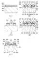
以下に、図9を参照しながら従来のLOCOS法を用いて素子分離を行った不揮発性半導体記憶装置について説明する。図9は、LOCOS法を用いて素子分離を行った従来のスタックゲート型EEPROMメモリセルのワード線(制御ゲート)に沿った方向の断面図を示す。
【0007】
図9において、シリコン基板301上にLOCOS法により素子分離酸化膜302が形成され、素子分離酸化膜302の間の素子領域には、トンネル酸化膜303を介して多結晶シリコン膜からなる浮遊ゲート304が形成され、さらに、浮遊ゲート304上には、絶縁膜305を介して多結晶シリコン膜からなるワード線(制御ゲート)306が形成されている。
【0008】
このような構成では、LOCOS法を用いて素子分離を行っているために、上記のような問題が微細化及び高集積化の妨げとなっていた。特に、EEPROMやフラッシュメモリの場合には、書き込みや消去の際に、ワード線306に5V以上の高電圧が印加されるために、素子分離酸化膜302の下に寄生チャネルが形成されやすく、特別の配慮が必要である。
【0009】
そこで、図10に示すようなトレンチ素子分離法が提案されている。図10は、トレンチ素子分離法を適用したスタックゲート型EEPROMメモリセルのワード線に沿った方向の断面図を示す。
【0010】
図10において、シリコン基板401上にトンネル酸化膜層404を介して多結晶シリコン層からなる浮遊ゲート405が形成され、さらに、浮遊ゲート405上には絶縁層406を介して多結晶シリコン層からなる制御ゲート407が形成されている。そして、シリコン基板401、浮遊ゲート405及び制御ゲート407はトレンチ(溝)409によってメモリセル毎に素子分離され、トレンチ409はトレンチ絶縁膜403を介してBPSG膜402によって埋め込まれ、制御ゲート407はタングステンシリサイドのワード線408に接続されている。
【0011】
この構造では、トレンチ409によって、素子領域を分離すると同時に、浮遊ゲート405及び制御ゲート407もメモリセル毎に分離しており、微小なセル面積を実現するものと期待されている。
【0012】
【発明が解決しようとする課題】
しかしながら、図10に示したようなトレンチ素子分離法では、基板にトレンチ(溝)を形成しなければならないために、製造工程が複雑になるという問題があった。また、トレンチの加工時に発生する欠陥の制御も困難であった。
【0013】
また、携帯用機器などを主体とするフラッシュメモリの適用分野を考えた場合、電源電圧を低電圧化し、書き換え動作を高速化することも重要である。このため、単体のメモリセルの動作を考えた場合、トンネル酸化膜に実際に印加される電圧が、ホットエレクトロン注入やFNトンネリングの効率に影響を及ぼし、電源電圧の低電圧化などを行う場合に重要となってくる。
【0014】
すなわち、トンネル酸化膜には制御ゲート電極に印加される電圧がそのまま印加されるのではなく、例えば書き込み動作時において実際にトンネル酸化膜に印加される電圧VPROGは以下の式に示されるように制御ゲート電極に印加される電圧よりも低い値となる。
【0015】
VPROG=KPROG×VCG …(1)
KPROG=CFC/(CFC+CFCH+CFD+CFS) …(2)
ここで、KPROG:書き込み動作時の容量結合比
VCG :制御ゲート電極に印加される電圧
CFC :制御ゲート電極と浮遊ゲート電極間の容量
CFCH:浮遊ゲート電極とチャネル領域間の容量
CFD :浮遊ゲート電極とドレイン拡散層間の容量
CFS :浮遊ゲート電極とソース拡散層間の容量
である。
【0016】
従って、例えば書き込み動作において、ホットエレクトロン注入やFNトンネリングの効率を向上させるためには、容量結合比(カップリングレシオ)を大きくするようにメモリセルの構造を最適化することが必要である。
【0017】
このため、(2)式から明らかなように、容量結合比を大きくして制御ゲート電極に供給する電圧を低電圧化し、書き換え速度を速くするためには、制御ゲート電極と浮遊ゲート電極とがオーバーラップする領域の面積を大きくすることが効果的である。
【0018】
そこで、本発明の目的は、LOCOS法やトレンチ素子分離法で素子分離された場合のような欠点を持たず、書き込み時の電圧を低くするとともに高集積化が可能な不揮発性半導体記憶装置及びその製造方法を提供することである。
【0019】
【課題を解決するための手段】
本発明に係る第1の不揮発性半導体記憶装置の製造方法は、第1導電型の半導体基板上に、第1の絶縁膜、第1の導電膜、第2の絶縁膜及び第3の絶縁膜を順次形成する工程と、前記第1の絶縁膜、前記第1の導電膜、前記第2の絶縁膜及び前記第3の絶縁膜を第1の方向に延びる形状にパターニングすることにより、前記半導体基板の表面の一部を露出する工程と、前記第1の絶縁膜、前記第1の導電膜、前記第2の絶縁膜及び前記第3の絶縁膜の側面にサイドウォール絶縁膜を形成する工程と、前記第1の絶縁膜、前記第1の導電膜、前記第2の絶縁膜、前記第3の絶縁膜及び前記サイドウォール絶縁膜から露出している半導体基板の表面にトンネル絶縁膜を形成する工程と、第2の導電膜を全面に形成する工程と、前記第2の導電膜の一部を前記第3の絶縁膜上で除去することにより、浮遊ゲート電極を形成する工程と、前記第3の絶縁膜の前記浮遊ゲート電極下の部分の少なくとも一部を除去することにより、前記浮遊ゲート電極下に隙間を形成する工程と、前記浮遊ゲート電極の露出した面全体を、前記隙間を残しながら覆う第4の絶縁膜を形成する工程と、前記隙間を埋める第3の絶縁膜を全面に形成する工程と、前記第3の導電膜、前記第4の絶縁膜及び前記浮遊ゲート電極を、前記第1の方向と交差する第2の方向に延びる形状にパターニングすることにより、前記浮遊ゲート電極との間で前記第4の絶縁膜を挟む制御ゲート電極を前記第3の導電膜から形成すると共に、前記半導体基板の表面の一部を露出する工程と、前記半導体基板の露出している部分に第2導電型の不純物を導入することにより、ソース拡散層及びドレイン拡散層を形成する工程と、を有することを特徴とする。
【0020】
ここで、前記ソース拡散層及びドレイン拡散層を形成する工程は、前記半導体基板の露出している部分にイオン注入を行う工程を有してもよい。
【0021】
本発明に係る第2の不揮発性半導体記憶装置の製造方法は、第1導電型の半導体基板上に、第1の絶縁膜、第1の導電膜、第2の絶縁膜及び第3の絶縁膜を順次形成する工程と、前記第1の絶縁膜、前記第1の導電膜、前記第2の絶縁膜及び前記第3の絶縁膜を第1の方向に延びる形状にパターニングすることにより、前記半導体基板の表面の一部を露出する工程と、前記第1の絶縁膜の脇に沿って前記半導体基板の表面に第2導電型の不純物を導入することにより、ソース拡散層及びドレイン拡散層を形成すると共に、これらの間にチャネル領域を形成する工程と、前記第1の絶縁膜、前記第1の導電膜、前記第2の絶縁膜及び前記第3の絶縁膜の側面にサイドウォール絶縁膜を形成する工程と、前記第1の絶縁膜、前記第1の導電膜、前記第2の絶縁膜、前記第3の絶縁膜及び前記サイドウォール絶縁膜から露出している半導体基板の表面にトンネル絶縁膜を形成する工程と、第2の導電膜を全面に形成する工程と、前記第2の導電膜の一部を前記第3の絶縁膜上で除去することにより、浮遊ゲート電極を形成する工程と、前記第3の絶縁膜の前記浮遊ゲート電極下の部分の少なくとも一部を除去することにより、前記浮遊ゲート電極下に隙間を形成する工程と、前記浮遊ゲート電極の露出した面全体を、前記隙間を残しながら覆う第4の絶縁膜を形成する工程と、前記隙間を埋める第3の絶縁膜を全面に形成する工程と、前記第3の導電膜、前記第4の絶縁膜及び前記浮遊ゲート電極を、前記第1の方向と交差する第2の方向に延びる形状にパターニングすることにより、前記浮遊ゲート電極との間で前記第4の絶縁膜を挟む制御ゲート電極を前記第3の導電膜から形成する工程と、を有することを特徴とする。
【0022】
ここで、前記ソース拡散層及びドレイン拡散層を形成する工程は、前記第2の方向からの斜めイオン注入を行う工程を有してもよい。
【0023】
また、前記第2の絶縁膜及びサイドウォール絶縁膜がシリコン酸化膜からなり、前記第3の絶縁膜がシリコン窒化膜からなることが好ましい。
【0024】
更に、前記第4の絶縁膜として、順次積層されたシリコン窒化膜、シリコン酸化膜及びシリコン窒化膜からなる積層体を形成することが好ましい。
【0029】
【実施例】
以下、本発明の第1実施例による不揮発性半導体記憶装置を図1及び図2を参照しながら説明する。図1は本発明の第1実施例によるメモリセルのパターンを示す平面図であり、図2は図1のA−A線で切断した断面図である。
【0030】
図2において、P型シリコン基板101上には、素子分離を行うシールドゲート電極103がシールドゲート絶縁膜102を介して形成されており、シールドゲート電極103に所定の電圧を印加することによりシールドゲート電極103の間に形成される素子領域を互いに電気的に分離する。また、サイドウォール酸化膜107がシールドゲート電極103の側面に形成されるとともにシールドキャップ酸化膜104がシールドゲート電極103の上面に形成されている。
【0031】
シールドゲート電極103によって素子分離されたチャネル領域には、トンネル酸化膜108として50〜130Å程度の膜厚のシリコン酸化膜が熱酸化によって形成され、トンネル酸化膜108の上部には、浮遊ゲート電極109として導電性の多結晶シリコン膜がシールドゲート電極103上に跨がるとともに隙間領域105′′を有するように形成されている。
【0032】
浮遊ゲート電極109の上面、側面及びシールドゲート電極103上に跨がった部分の浮遊ゲート電極109の下面には、層間絶縁膜110として例えばシリコン酸化膜/シリコン窒化膜/シリコン酸化膜からなる酸化膜厚換算で150〜200Å程度の膜厚のONO絶縁膜が形成され、層間絶縁膜110の外周部には、制御ゲート電極111として導電性の多結晶シリコン膜が隙間領域105′′を埋め込むように形成されている。
【0033】
また、図1のA−A線と直交する方向では、浮遊ゲート電極109の両側にN型のドレイン拡散層113及びソース拡散層114が形成されており、ドレイン拡散層113及びソース拡散層114は2つの浮遊ゲート電極109で共有されている。ドレイン拡散層113及びソース拡散層114には、不純物として砒素が1×10¹⁸〜1×1021cm-3程度の表面濃度で導入されている。また、ドレイン拡散層113は、ドレインコンタクト115を介して不図示の金属配線層に接続されており、ソース拡散層114もソースコンタクト116を介して不図示の金属配線層に接続されている。
【0034】
次に、本発明の第1実施例による不揮発性半導体記憶装置の動作を図3を参照しながら説明する。図3は、本発明の第1実施例による不揮発性半導体記憶装置のメモリセルアレイの一部を等価的に示す回路図である。
【0035】
書き込み時において、例えばメモリセルトランジスタT3を選択する場合、図示しないデコーダにより例えばビット線D0に6V、ビット線D1に0V、ソース線S0に0V、ワード線W1に10V、ワード線W0、W2に0Vを印加することにより、メモリセルトランジスタT3のドレイン拡散層113に6V、ソース拡散層114に0V、制御ゲート電極111に10Vの電圧を与える。
【0036】
このため、メモリセルトランジスタT3のチャネル領域に電流が流れ、ドレイン拡散層113の近傍のチャネル領域に生成されたピンチオフ領域において電界により加速された電子がホットエレクトロンとなり、トンネル酸化膜108のエネルギー障壁を越えて浮遊ゲート電極109に注入される。注入された電子は、電気的に浮遊状態にある浮遊ゲート電極109中に保持されるので、メモリセルトランジスタT3のしきい値電圧は、例えば初期状態の2V程度から7V程度に上昇し書き込みが行われる。
【0037】
また、消去時において、図示しないデコーダにより例えばビット線D0、D1を開放にし、ソース線S0に12V、ワード線W0〜W2に0Vを印加することにより、ドレイン拡散層113を浮遊状態とし、ソース拡散層114に12V、制御ゲート電極111に0Vの電圧を与える。
【0038】
このため、浮遊ゲート電極109中の電子が、FNトンネリングによりトンネル酸化膜108を介してソース拡散層114に引き抜かれ、メモリセルトランジスタT3〜T6のしきい値電圧は例えば7V程度から2V程度に下降しセクター消去が行われる。
【0039】
また、読み出し時においては、例えばメモリセルトランジスタT3を選択する場合、図示しないデコーダにより例えばビット線D0に1V、ビット線D1に0V、ソース線S0に0V、ワード線W1に5V、ワード線W0、W2に0Vを印加することにより、メモリセルトランジスタT3のドレイン拡散層113に1V、ソース拡散層114に0V、制御ゲート電極111に5Vの電圧を与え、メモリセルトランジスタT3に電流が流れるかどうかを不図示のセンスアンプにより検出する。
【0040】
この第1実施例において、書き込み時に制御ゲート電極111に印加する電圧を従来の12V程度から10V程度に減少でき、動作時における低電圧化が可能となる。
【0041】
以上説明したように、本発明の第1実施例による不揮発性半導体記憶装置によれば、素子分離領域にシールドゲート絶縁膜102を介してシールドゲート電極103を形成し、シールドゲート電極103に例えば電源電圧Vccなどの所定の電圧を印加することによりシールドゲート電極103の間に形成される素子領域を互いに電気的に分離しているので、LOCOS法に比べて素子領域における寸法シフトを抑制でき、メモリセルの面積を縮小できる。また、素子分離領域にチャネルストップ不純物層を形成する必要がないため素子間の狭チャネル効果を抑制できる。さらに、シールドゲート電極103は基準電位に固定されるため、ワード線に高電圧が印加された場合でも、寄生チャネルが発生することを防止できる。また、浮遊ゲート電極109の上下面から制御電圧を印加することにより、セルサイズを大きくすることなく浮遊ゲート電極109と制御ゲート電極111との容量結合比を向上でき、低電圧の書き込みが可能となる。
【0042】
次に、本発明の第1実施例による不揮発性半導体記憶装置の製造方法を図4を参照しながら説明する。図4は、本発明の第1実施例による不揮発性半導体記憶装置の製造方法を工程順に示す断面図である。
【0043】
まず、図4(a)に示すように、P型シリコン基板101に熱酸化法又はCVD法によって、厚みが50〜100nm程度のシリコン酸化膜102′を形成する。そして、CVD法によって、厚みが100〜300nm程度のP又はN型にドープされた多結晶シリコン膜103′、厚みが100〜300nm程度のシリコン酸化膜104′、厚みが100〜200nm程度のシリコン窒化膜105′を順次形成する。
【0044】
次に、図4(b)に示すように、シリコン酸化膜102′、多結晶シリコン膜103′、シリコン酸化膜104′、シリコン窒化膜105′をフォトリソグラフィー及び異方性ドライエッチングによってパターニングし、素子分離領域にシールドゲート酸化膜102、シールドゲート電極103、シールドキャップ酸化膜104、シールドキャップ窒化膜105を形成する。その後、厚みが100〜300nm程度のシリコン酸化膜を全面に堆積し、異方性ドライエッチングを施すことにより、サイドウォール酸化膜107をシールドゲート電極103の側壁に形成する。
【0045】
次に、図4(c)に示すように、ウエットエッチングにより素子領域のP型シリコン基板11の表面を露出させた後、熱酸化法によってトンネル酸化膜108として10nm程度の膜厚のシリコン酸化膜を形成する。なお、トンネル酸化膜108として酸化膜を急速熱処理法を用いて窒化した酸窒化膜を使用してもよい。その後、100〜300nm程度の膜厚の導電性多結晶シリコン膜をCVD法などにより形成し、フォトリソグラフィー及びドライエッチングにより、シールドゲート電極103上において前記多結晶シリコン膜を図1のA−A方向に分離させて浮遊ゲート電極109を形成する。
【0046】
次に、図4(d)に示すように、熱リン酸を用いたウエットエッチングによりシールドキャップ窒化膜105の少なくとも一部を除去し、浮遊ゲート電極109とシールドキャップ酸化膜104との間に隙間領域15′′を形成する。その後、浮遊ゲート電極109の上部、側部及び隙間領域15′′における浮遊ゲート電極109の下面上に、層間絶縁膜110として例えばシリコン酸化膜/シリコン窒化膜/シリコン酸化膜からなる酸化膜厚換算で15〜20nm程度の膜厚のONO絶縁膜を形成する。なお、ONO絶縁膜の下層のシリコン酸化膜はCVD法又は900〜1000℃の熱酸化法により10nm程度の膜厚に形成し、シリコン窒化膜はCVD法により10nm程度の膜厚に形成し、ONO絶縁膜の上層のシリコン酸化膜はCVD法又は900〜1000℃の熱酸化法により5nm程度の膜厚に形成する。
【0047】
次に、図4(e)に示すように、CVD法などにより層間絶縁膜110の表面を覆うように導電性の多結晶シリコン膜を形成した後、フォトリソグラフィー及びドライエッチングにより前記多結晶シリコン膜を図1のA−A方向と直交する方向に分離させ、制御ゲート電極111を形成する。この時、浮遊ゲート電極109及び層間絶縁膜110も同時にエッチングを行い、浮遊ゲート電極109及び層間絶縁膜110も図1のA−A方向と直交する方向に分離させる。なお、制御ゲート電極111は、シート抵抗の低減のためポリサイドやシリサイド構造としてもよい。
【0048】
次に、制御ゲート電極111をマスクとして砒素などの不純物を注入エネルギー50〜90keV、ドーズ量5×1015cm-2の条件でイオン注入することにより、図1のN型のドレイン拡散層113及びソース拡散層114を形成する。そして、CVD法により層間絶縁膜として燐及びボロンを含んだシリコン酸化膜(BPSG膜)を形成し、ドレインコンタクト115及びソースコンタクト116を開口した後、スパッタ法によってAl−Si−Cuなどの金属配線層を形成する。
【0049】
以上により、簡便な方法で浮遊ゲート電極109の上面及び下面の一部に制御ゲート電極111を形成できるとともに寸法シフトの発生しない素子分離領域を形成できる。
【0050】
次に、本発明の第2実施例による不揮発性半導体記憶装置を図5及び図6を参照しながら説明する。図5は本発明の第2実施例によるメモリセルのパターンを示す平面図であり、図6は図5のA−A線で切断した断面図である。
【0051】
図6において、P型シリコン基板201上には、素子分離を行うシールドゲート電極203がシールドゲート絶縁膜202を介して形成されており、シールドゲート電極203に所定の電圧を印加することによりシールドゲート電極203の間に形成される素子領域を互いに電気的に分離する。また、サイドウォール窒化膜207がシールドゲート電極203の側面に形成されるとともにシールドキャップ酸化膜204がシールドゲート電極203の上面に形成されている。さらに、シールドゲート電極203の下方のP型シリコン基板201にはソース/ドレインとなる埋め込み拡散層206が形成されている。この埋め込み拡散層206は、浮遊ゲート電極209の一部の領域にオーバーラップするように形成されており、不純物として砒素が1×1018〜1×1021cm-3程度の表面濃度で導入されている。
【0052】
シールドゲート電極203によって素子分離されたチャネル領域には、トンネル酸化膜208として50〜130Å程度の膜厚のシリコン酸化膜が熱酸化により形成され、トンネル酸化膜208の上部に浮遊ゲート電極209として導電性の多結晶シリコン膜が隙間領域205′′を有するようにシールドゲート電極203に跨がって形成されている。
【0053】
浮遊ゲート電極209の上面、側面及びシールドゲート電極203上に跨がった部分の浮遊ゲート電極209の下面には、層間絶縁膜210として例えばシリコン酸化膜/シリコン窒化膜/シリコン酸化膜からなる酸化膜厚換算で150〜200Å程度の膜厚のONO絶縁膜が形成され、層間絶縁膜210の外周部には、制御ゲート電極211として導電性の多結晶シリコン膜が隙間領域205′′を埋め込むように形成されている。
【0054】
図5に示すように、埋め込み拡散層206は、ワード線に直交する方向のメモリセルに共通に形成されている。そして、埋め込み拡散層206の一方(ドレイン)は、所定ブロック毎に設けられたビットコンタクトを介してビット線に接続しており、他方(ソース)は、やはり所定ブロック毎に設けられたソースコンタクトを介してソース線に接続されている。すなわち、各ブロック内では、シリコン基板201内の埋め込み拡散層206の一方(ドレイン)がビット線を構成し、他方(ソース)がソース線を構成している。このような構成により、各メモリセルにおけるビットコンタクト及びソースコンタクトが不要となり、その結果、各メモリセルの面積縮小が可能となる。
【0055】
次に、本発明の第2実施例による不揮発性半導体記憶装置の動作を図7を参照しながら説明する。図7は本発明の第2実施例による不揮発性半導体記憶装置を等価的に示す回路図である。
【0056】
書き込み時において、例えばメモリセルトランジスタT5を選択する場合、図示しないデコーダにより例えばビット線D1に3V、ビット線D0、D2に0V、ソース線S0に0V、ワード線W1に−9V、ワード線W0、W2、W3に0V、基板201に0V、選択ワード線SW1に3V、選択ワード線SW2に0Vを印加することにより、選択トランジスタST2をオン、選択トランジスタST5をオフさせ、メモリセルトランジスタT5のソース拡散層を浮遊状態とし、ドレイン拡散層に3V、、制御ゲート電極211に−9Vの電圧を与える。
【0057】
このため、FNトンネリングにより浮遊ゲート電極209中の電子がドレイン拡散層に引き抜かれメモリセルトランジスタT5の書き込みが行われる。
【0058】
また、消去時において、図示しないデコーダにより例えばビット線D0〜D2に0V、ソース線S0に0V、ワード線W1に13V、ワード線W0、W2、W3に0V、基板201に0V、選択ワード線SW1、SW2に3Vを印加することにより、選択トランジスタST2、ST5をオンさせ、ドレイン拡散層及びソース拡散層に0V、制御ゲート電極211に0Vの電圧を与える。
【0059】
このため、FNトンネリングにより基板201からワード線W1に接続されているメモリセルトランジスタT4〜T6に電子が注入され、セクター消去がおこなわれる。
【0060】
また、読み出し時においては、例えばメモリセルトランジスタT5を選択する場合、図示しないデコーダにより例えばビット線D1に1V、ビット線D0、D2に0V、ソース線S0に0V、ワード線W1に3V、ワード線W0、W2、W3に0V、基板201に0V、選択ワード線SW1、SW2に3Vを印加することにより、選択トランジスタST2、ST5をオンさせ、メモリセルトランジスタT5のドレイン拡散層に1V、ソース拡散層に0V、制御ゲート電極211に3Vの電圧を与え、メモリセルトランジスタT5に電流が流れるかどうかを不図示のセンスアンプで検出する。
【0061】
この第2実施例において、制御ゲート電極211と浮遊ゲート電極209の容量結合比が向上しているので、書き込み時における制御ゲート電極211に印加する電圧を減少でき、動作時における低電圧化が可能となる。
【0062】
以上説明したように、本発明の第2実施例による不揮発性半導体記憶装置によれば、素子分離領域にシールドゲート絶縁膜202を介してシールドゲート電極203を形成し、シールドゲート電極203に所定の電圧を印加することによりシールドゲート電極203の間に形成される素子領域を互いに電気的に分離するとともにソース/ドレインを埋め込み拡散層206としてドレインコンタクトやソースコンタクトをなくすようにしたので、従来に比べてメモリセルの面積のより一層の縮小が可能になる。また、浮遊ゲート電極209の上下面から制御電圧を印加することにより、セルサイズを大きくすることなく浮遊ゲート電極209と制御ゲート電極211との容量結合比を向上でき、低電圧の書き込みが可能となる。
【0063】
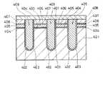
次に、本発明の第2実施例による製造方法を図8を参照しながら説明する。図8は、本発明の第2実施例による製造方法を工程順に示す概略断面図である。
【0064】
まず、図8(a)に示すように、P型シリコン基板201に熱酸化法又はCVD法によって、厚みが50〜100nm程度のシリコン酸化膜202′を形成する。そして、CVD法によって、厚みが100〜300nm程度のP又はN型にドープされた多結晶シリコン膜203′、厚みが100〜300nm程度のシリコン酸化膜204′、厚みが100〜200nm程度のシリコン窒化膜205′を順次形成する。
【0065】
次に、図8(b)に示すように、シリコン酸化膜202′、多結晶シリコン膜203′、シリコン酸化膜204′、シリコン窒化膜205′をフォトリソグラフィー及び異方性ドライエッチングによってパターニングし、素子分離領域にシールドゲート酸化膜202、シールドゲート電極203、シールドキャップ酸化膜204、シールドキャップ窒化膜205を形成する。
【0066】
次に、図8(c)に示すように、斜めイオン注入212によりシールドゲート酸化膜202、シールド電極203、シールドキャップ絶縁膜204、シールドキャップ窒化膜205をマスクとしてシリコン基板201内に砒素を打ち込み、埋め込み拡散層206を形成する。この時の条件としては、砒素を打ち込む場合、エネルギーを50〜90keV、ドーズ量を5×1015cm-2に設定する。
【0067】
さらに、打ち込みの角度θは、シールドゲート酸化膜202、シールド電極203、シールドキャップ絶縁膜204、シールドキャップ窒化膜205の膜厚の合計(高さ)をa、間隔をbとすると、
θ=tan-1(a/b)
で与えられる。例えば、シールドゲート酸化膜202、シールド電極203、シールドキャップ絶縁膜204、シールドキャップ窒化膜205の厚みがそれぞれ50nm、100nm、100nm、100nm(a=0.35μm)で、間隔bが1μmの時、打ち込みの角度θはおよそ20〜21°となり、シールドゲート酸化膜202、シールド電極203、シールドキャップ絶縁膜204、シールドキャップ窒化膜205の厚みがそれぞれ100nm、300nm、200nm、300nm(a=0.9μm)で、間隔bが1μmの時、打ち込みの角度θはおよそ42〜45°となる。
【0068】
このように基板201に対して斜め方向からイオン注入212を行うことにより、シールドゲート酸化膜202、シールド電極203、シールドキャップ絶縁膜204、シールドキャップ窒化膜205がマスクとなって、それらの端部近傍部分に、互いに離隔した埋め込み拡散層206が自己整合的に形成される。そして、この時打ち込まれた不純物が後の熱処理によって若干横方向に拡散し、シールドゲート酸化膜202の下方に一部が重なった形の埋め込み拡散層206が形成される。
【0069】
次に、図8(d)に示すように、厚みが100〜300nm程度のシリコン窒化膜を全面に堆積し、異方性ドライエッチングを施すことにより、サイドウォール窒化膜207をシールドゲート電極203の側壁に形成する。その後、ウエットエッチングにより素子領域のP型シリコン基板201の表面を露出させた後、熱酸化法によってトンネル酸化膜208として10nm程度の膜厚のシリコン酸化膜を形成する。この時、シールド電極203を構成する多結晶シリコンも同時に酸化されないようにするため、シールドキャップ絶縁膜204及びサイドウォール窒化膜207は、いずれも、耐酸化性を有するシリコン窒化膜で構成するのが望ましいが、一方又は両方ともシリコン酸化膜であってもよい。なお、トンネル酸化膜208として酸化膜を急速熱処理法を用いて窒化した酸窒化膜を使用してもよい。その後、100〜300nm程度の膜厚の導電性多結晶シリコン膜をCVD法などにより形成し、フォトリソグラフィー及びドライエッチングにより、シールドゲート電極203上において前記多結晶シリコン膜を図5のB−B方向に分離させて浮遊ゲート電極209を形成する。
【0070】
次に、図8(e)に示すように、熱リン酸を用いたウエットエッチングによりシールドキャップ窒化膜205の少なくとも一部を除去し、浮遊ゲート電極209とシールドキャップ酸化膜204との間に隙間領域205′′を形成する。その後、浮遊ゲート電極109の上部、側部及び隙間領域205′′における浮遊ゲート電極209の下面上に、層間絶縁膜210として例えばシリコン酸化膜/シリコン窒化膜/シリコン酸化膜からなる酸化膜厚換算で15〜20nm程度の膜厚のONO絶縁膜を形成する。なお、ONO絶縁膜の下層のシリコン酸化膜はCVD法又は900〜1000℃の熱酸化法により10nm程度の膜厚に形成し、シリコン窒化膜はCVD法により10nm程度の膜厚に形成し、ONO絶縁膜の上層のシリコン酸化膜はCVD法又は900〜1000℃の熱酸化法により5nm程度の膜厚に形成する。
【0071】
次に、CVD法などにより層間絶縁膜210の表面を覆うように導電性の多結晶シリコン膜を形成した後、フォトリソグラフィー及びドライエッチングにより前記多結晶シリコン膜を図5のB−B方向と直交する方向に分離させ、制御ゲート電極211を形成する。この時、浮遊ゲート電極209及び層間絶縁膜210も同時にエッチングを行い、浮遊ゲート電極209及び層間絶縁膜210も図5のB−B方向と直交する方向に分離させる。なお、制御ゲート電極211は、シート抵抗の低減のためポリサイドやシリサイド構造としてもよい。
【0072】
以上により、簡便な方法で浮遊ゲート電極209の上面及び下面の一部に制御ゲート電極211を形成できるとともにソース/ドレインを埋め込み拡散層206としてドレインコンタクトやソースコンタクトをなくすことができる。
【0073】
また、本発明は、記憶装置に限らずゲート、ソース及びドレインを有する各種半導体装置の製造方法に適用が可能である。それらの場合、上述した製造方法において、ゲート構造の形成方法のみを異ならせればよい。例えば、MOSトランジスタを形成する場合、図8(d)〜(e)の工程において、シリコン基板201の表面にゲート酸化膜を形成した後、その上に、多結晶シリコン膜等からなるゲート配線をパターン形成すればよい。
【0074】
さらに、以上に説明した実施例では、浮遊ゲート108、208を有するスタックゲート型EEPROMの場合を説明したが、本発明は、同様に高電圧を印加するMNOS型の不揮発性半導体記憶装置についても、殆ど同様にして適用が可能である。
【0075】
【発明の効果】
以上説明したように、本発明によれば、シールドゲート絶縁膜を介して形成されたシールドゲート電極に所定の電圧を印加することによって素子分離を行うとともに、制御ゲート電極の一部の領域が浮遊ゲート電極の下面に絶縁膜を介して接するようにしたので、メモリセルの面積を大きくすることなしに容量結合比を大きくすることができ、メモリセルの動作時における低電圧化及び、高速化が可能となる。
【図面の簡単な説明】
【図1】本発明の第1実施例による不揮発性半導体記憶装置のメモリセルのパターンを示す平面図である。
【図2】本発明の第1実施例による不揮発性半導体記憶装置のメモリセルの構造を示す断面図である。
【図3】本発明の第1実施例による不揮発性半導体記憶装置を等価的に示す回路図である。
【図4】本発明の第1実施例による不揮発性半導体記憶装置の製造方法を工程順に示す断面図である。
【図5】本発明の第2実施例による不揮発性半導体記憶装置のメモリセルのパターンを示す平面図である。
【図6】本発明の第2実施例による不揮発性半導体記憶装置のメモリセルの構造を示す断面図である。
【図7】本発明の第2実施例による不揮発性半導体記憶装置を等価的に示す回路図である。
【図8】本発明の第2実施例による不揮発性半導体記憶装置の製造方法を工程順に示す断面図である。
【図9】従来の不揮発性半導体記憶装置のメモリセルの構造を示す断面図である。
【図10】従来の不揮発性半導体記憶装置のメモリセルの構造を示す断面図である。
【符号の説明】
101、201 P型シリコン半導体基板
102、202 シールドゲート絶縁膜
102′、202′ シリコン酸化膜
103、203 シールドゲート電極
103′、203′ 多結晶シリコン膜
104、204 シールドキャップ酸化膜
104′、204′ シリコン酸化膜
105、205 シールドキャップ窒化膜
105′、205′ シリコン窒化膜
105′′、205′′ 隙間領域
206 埋め込み拡散層
107 サイドウォール酸化膜
207 サイドウォール窒化膜
108、208 トンネル酸化膜
109、209 浮遊ゲート電極
110、210 層間絶縁膜
111、211 制御ゲート電極
113 ドレイン拡散層
114 ソース拡散層
115 ドレインコンタクト
116 ソースコンタクト
T1〜T12 メモリセルトランジスタ
ST1〜ST6 選択トランジスタ
D0〜D2 ビット線
W0〜W3 ワード線
S0 ソース線
SW1、SW2 選択ワード線[0001]
BACKGROUND OF THE INVENTION
The present invention relates to a method for manufacturing a nonvolatile semiconductor memory device capable of electrically writing and erasing data, and is suitable for use in manufacturing a nonvolatile semiconductor memory device having stack gate type memory cells.
[0002]
[Prior art]
Conventionally, EEPROM (Electrically Erasable Programmable Read Only) is a nonvolatile semiconductor memory device that can electrically write and erase data.
Memory) and flash memory are known.
[0003]
In particular, a flash memory having a stack gate type memory cell structure can be composed of a single floating gate type transistor, so that the manufacturing process can be simplified, the unit price per bit can be reduced, and high integration and large capacity can be achieved. Therefore, it is widely used mainly for replacement of magnetic recording media such as hard disks and floppy disks.
[0004]
There is a selective oxidation method such as a LOCOS method as an element isolation method that has been conventionally used in semiconductor devices such as these nonvolatile semiconductor memory devices. The LOCOS method has an advantage that the manufacturing method is simple and the occurrence of defects is relatively easy to control because the slope at the boundary between the element isolation region and the element region is gentle.
[0005]
However, as devices are miniaturized due to the demand for higher integration, the following problems have arisen. In other words, from the viewpoint of processing, there are problems of element isolation pitch and element isolation oxide film thickness related to the occurrence of bird's beaks. Further, from the viewpoint of electrical characteristics, there are problems of field inversion, narrow channel effect and punch-through related to the lateral diffusion of impurities.
[0006]
Hereinafter, a nonvolatile semiconductor memory device in which element isolation is performed using the conventional LOCOS method will be described with reference to FIG. FIG. 9 shows a cross-sectional view in the direction along the word line (control gate) of a conventional stack gate type EEPROM memory cell in which element isolation is performed using the LOCOS method.
[0007]
In FIG. 9, an element
[0008]
In such a configuration, since element isolation is performed using the LOCOS method, the above-described problems hinder miniaturization and high integration. In particular, in the case of an EEPROM or a flash memory, since a high voltage of 5 V or more is applied to the
[0009]
Therefore, a trench element isolation method as shown in FIG. 10 has been proposed. FIG. 10 is a cross-sectional view in the direction along the word line of the stacked gate type EEPROM memory cell to which the trench element isolation method is applied.
[0010]
In FIG. 10, a
[0011]
In this structure, the element region is separated by the
[0012]
[Problems to be solved by the invention]
However, the trench element isolation method as shown in FIG. 10 has a problem that the manufacturing process becomes complicated because a trench (groove) must be formed in the substrate. In addition, it is difficult to control defects that occur during trench processing.
[0013]
In addition, considering the application field of flash memory mainly composed of portable devices, it is also important to reduce the power supply voltage and speed up the rewriting operation. Therefore, when considering the operation of a single memory cell, the voltage actually applied to the tunnel oxide film affects the efficiency of hot electron injection and FN tunneling, and the power supply voltage is lowered. It becomes important.
[0014]
That is, the voltage applied to the control gate electrode is not applied as it is to the tunnel oxide film, but for example, the voltage V actually applied to the tunnel oxide film during the write operation.PROG Is a value lower than the voltage applied to the control gate electrode as shown in the following equation.
[0015]
VPROG = KPROG × VCG ... (1)
KPROG = CFC / (CFC + CFCH + CFD + CFS (2)
Where KPROG : Capacitive coupling ratio during write operation
VCG : Voltage applied to the control gate electrode
CFC : Capacitance between control gate electrode and floating gate electrode
CFCH : Capacitance between floating gate electrode and channel region
CFD : Capacitance between floating gate electrode and drain diffusion layer
CFS : Capacitance between floating gate electrode and source diffusion layer
It is.
[0016]
Therefore, for example, in order to improve the efficiency of hot electron injection and FN tunneling in the write operation, it is necessary to optimize the structure of the memory cell so as to increase the capacitive coupling ratio (coupling ratio).
[0017]
For this reason, as is clear from the equation (2), in order to increase the capacitive coupling ratio to lower the voltage supplied to the control gate electrode and increase the rewriting speed, the control gate electrode and the floating gate electrode are It is effective to increase the area of the overlapping region.
[0018]
SUMMARY OF THE INVENTION Accordingly, an object of the present invention is to provide a non-volatile semiconductor memory device capable of reducing the voltage at the time of writing and achieving high integration without having the drawbacks when the elements are isolated by the LOCOS method or the trench element isolation method. It is to provide a manufacturing method.
[0019]
[Means for Solving the Problems]
According to the first non-volatile semiconductor memory device manufacturing method of the present invention, a first insulating film, a first conductive film, a second insulating film, and a third insulating film are formed on a first conductive type semiconductor substrate. And sequentially patterning the first insulating film, the first conductive film, the second insulating film, and the third insulating film into a shape extending in a first direction. Exposing a part of the surface of the substrate; and forming a sidewall insulating film on a side surface of the first insulating film, the first conductive film, the second insulating film, and the third insulating film. And forming a tunnel insulating film on the surface of the semiconductor substrate exposed from the first insulating film, the first conductive film, the second insulating film, the third insulating film, and the sidewall insulating film A step of forming a second conductive film on the entire surface, and a step of forming the second conductive film. Removing the portion on the third insulating film to form a floating gate electrode, and removing at least part of the portion of the third insulating film below the floating gate electrode to thereby form the floating gate electrode. Forming a gap below the gate electrode; forming a fourth insulating film covering the entire exposed surface of the floating gate electrode while leaving the gap; and covering the entire surface of the third insulating film filling the gap. And forming the floating gate by patterning the third conductive film, the fourth insulating film, and the floating gate electrode into a shape extending in a second direction intersecting the first direction. Forming a control gate electrode sandwiching the fourth insulating film with the electrode from the third conductive film, exposing a part of the surface of the semiconductor substrate, and exposing the semiconductor substrate; Second part By introducing conductive impurities, and having a step of forming a source diffusion layer and drain diffusion layer.
[0020]
Here, the step of forming the source diffusion layer and the drain diffusion layer may include a step of implanting ions into the exposed portion of the semiconductor substrate.
[0021]
According to the second non-volatile semiconductor memory device manufacturing method of the present invention, a first insulating film, a first conductive film, a second insulating film, and a third insulating film are formed on a first conductive type semiconductor substrate. And sequentially patterning the first insulating film, the first conductive film, the second insulating film, and the third insulating film into a shape extending in a first direction. Forming a source diffusion layer and a drain diffusion layer by exposing a part of the surface of the substrate, and introducing a second conductivity type impurity into the surface of the semiconductor substrate alongside the first insulating film; And a step of forming a channel region therebetween, and a sidewall insulating film on the side surfaces of the first insulating film, the first conductive film, the second insulating film, and the third insulating film. Forming the first insulating film; the first conductive film; Forming a tunnel insulating film on the surface of the semiconductor substrate exposed from the second insulating film, the third insulating film, and the sidewall insulating film; and forming a second conductive film over the entire surface; Removing a part of the second conductive film on the third insulating film to form a floating gate electrode; and at least a part of a part of the third insulating film under the floating gate electrode A step of forming a gap under the floating gate electrode, a step of forming a fourth insulating film covering the entire exposed surface of the floating gate electrode while leaving the gap, and the gap Forming a third insulating film to be buried on the entire surface, and extending the third conductive film, the fourth insulating film, and the floating gate electrode in a second direction intersecting the first direction; By patterning before Forming a control gate electrode sandwiching said fourth insulating film between the floating gate electrode from the third conductive film, and having a.
[0022]
Here, the step of forming the source diffusion layer and the drain diffusion layer may include a step of performing oblique ion implantation from the second direction.
[0023]
Preferably, the second insulating film and the sidewall insulating film are made of a silicon oxide film, and the third insulating film is made of a silicon nitride film.
[0024]
Furthermore, it is preferable to form a stacked body including a silicon nitride film, a silicon oxide film, and a silicon nitride film sequentially stacked as the fourth insulating film.
[0029]
【Example】
Hereinafter, a nonvolatile semiconductor memory device according to a first embodiment of the present invention will be described with reference to FIGS. FIG. 1 is a plan view showing a memory cell pattern according to a first embodiment of the present invention, and FIG. 2 is a cross-sectional view taken along the line AA of FIG.
[0030]
In FIG. 2, a
[0031]
In the channel region separated by the
[0032]
On the upper surface and side surfaces of the floating
[0033]
Further, in the direction orthogonal to the line AA in FIG. 1, an N-type
[0034]
Next, the operation of the nonvolatile semiconductor memory device according to the first embodiment of the present invention will be described with reference to FIG. FIG. 3 is a circuit diagram equivalently showing a part of the memory cell array of the nonvolatile semiconductor memory device according to the first embodiment of the present invention.
[0035]
At the time of writing, for example, when the memory cell transistor T3 is selected, a decoder (not shown), for example, 6V on the bit line D0, 0V on the bit line D1, 0V on the source line S0, 10V on the word line W1, 0V on the word lines W0 and W2. Is applied to the
[0036]
Therefore, current flows in the channel region of the memory cell transistor T3, and electrons accelerated by the electric field in the pinch-off region generated in the channel region near the
[0037]
At the time of erasing, for example, the bit lines D0 and D1 are opened by a decoder (not shown), 12V is applied to the source line S0, and 0V is applied to the word lines W0 to W2, thereby bringing the
[0038]
For this reason, electrons in the floating
[0039]
In reading, for example, when the memory cell transistor T3 is selected, a decoder (not shown), for example, 1V for the bit line D0, 0V for the bit line D1, 0V for the source line S0, 5V for the word line W1, By applying 0 V to W2, a voltage of 1 V is applied to the
[0040]
In the first embodiment, the voltage applied to the
[0041]
As described above, according to the nonvolatile semiconductor memory device according to the first embodiment of the present invention, the
[0042]
Next, a method for manufacturing the nonvolatile semiconductor memory device according to the first embodiment of the present invention will be described with reference to FIG. FIG. 4 is a cross-sectional view showing the method of manufacturing the nonvolatile semiconductor memory device according to the first embodiment of the present invention in the order of steps.
[0043]
First, as shown in FIG. 4A, a silicon oxide film 102 'having a thickness of about 50 to 100 nm is formed on a P-
[0044]
Next, as shown in FIG. 4B, the
[0045]
Next, as shown in FIG. 4C, after exposing the surface of the P-type silicon substrate 11 in the element region by wet etching, a silicon oxide film having a thickness of about 10 nm is formed as a
[0046]
Next, as shown in FIG. 4D, at least a part of the shield
[0047]
Next, as shown in FIG. 4E, a conductive polycrystalline silicon film is formed so as to cover the surface of the
[0048]
Next, using the
[0049]
As described above, the
[0050]
Next, a non-volatile semiconductor memory device according to a second embodiment of the present invention will be described with reference to FIGS. FIG. 5 is a plan view showing a memory cell pattern according to the second embodiment of the present invention, and FIG. 6 is a cross-sectional view taken along the line AA of FIG.
[0051]
In FIG. 6, a
[0052]
In the channel region isolated by the
[0053]
On the upper surface and side surfaces of the floating
[0054]
As shown in FIG. 5, the buried
[0055]
Next, the operation of the nonvolatile semiconductor memory device according to the second embodiment of the present invention will be described with reference to FIG. FIG. 7 is a circuit diagram equivalently showing a nonvolatile semiconductor memory device according to the second embodiment of the present invention.
[0056]
At the time of writing, for example, when the memory cell transistor T5 is selected, a decoder (not shown), for example, 3V for the bit line D1, 0V for the bit lines D0 and D2, 0V for the source line S0, -9V for the word line W1, By applying 0V to W2 and W3, 0V to the
[0057]
For this reason, electrons in the floating
[0058]
At the time of erasing, for example, 0 V is applied to the bit lines D0 to D2, 0 V to the source line S0, 13 V to the word line W1, 0 V to the word lines W0, W2, and W3, 0 V to the
[0059]
Therefore, electrons are injected from the
[0060]
In reading, for example, when the memory cell transistor T5 is selected, a decoder (not shown), for example, 1V on the bit line D1, 0V on the bit lines D0 and D2, 0V on the source line S0, 3V on the word line W1, By applying 0V to W0, W2, and W3, 0V to the
[0061]
In the second embodiment, since the capacitive coupling ratio between the
[0062]
As described above, according to the nonvolatile semiconductor memory device according to the second embodiment of the present invention, the
[0063]
Next, a manufacturing method according to the second embodiment of the present invention will be described with reference to FIG. FIG. 8 is a schematic sectional view showing the manufacturing method according to the second embodiment of the present invention in the order of steps.
[0064]
First, as shown in FIG. 8A, a
[0065]
Next, as shown in FIG. 8B, the
[0066]
Next, as shown in FIG. 8C, arsenic is implanted into the
[0067]
Further, the implantation angle θ is defined such that the total thickness (height) of the shield
θ = tan-1 (A / b)
Given in. For example, when the thickness of the shield
[0068]
Thus, by performing
[0069]
Next, as shown in FIG. 8D, a silicon nitride film having a thickness of about 100 to 300 nm is deposited on the entire surface, and anisotropic dry etching is performed to form the
[0070]
Next, as shown in FIG. 8E, at least a part of the shield
[0071]
Next, after a conductive polycrystalline silicon film is formed so as to cover the surface of the
[0072]
As described above, the
[0073]
The present invention is not limited to a memory device and can be applied to a method for manufacturing various semiconductor devices having a gate, a source, and a drain. In those cases, only the method for forming the gate structure is different in the manufacturing method described above. For example, when forming a MOS transistor, after forming a gate oxide film on the surface of the
[0074]
Furthermore, in the embodiment described above, the case of the stack gate type EEPROM having the floating
[0075]
【The invention's effect】
As described above, according to the present invention, element isolation is performed by applying a predetermined voltage to the shield gate electrode formed through the shield gate insulating film, and a part of the control gate electrode is floated. Since the lower surface of the gate electrode is in contact via an insulating film, the capacity coupling ratio can be increased without increasing the area of the memory cell, and the voltage and speed can be increased during operation of the memory cell. It becomes possible.
[Brief description of the drawings]
FIG. 1 is a plan view showing a memory cell pattern of a nonvolatile semiconductor memory device according to a first embodiment of the present invention;
FIG. 2 is a cross-sectional view showing a structure of a memory cell of a nonvolatile semiconductor memory device according to a first embodiment of the present invention.
FIG. 3 is a circuit diagram equivalently showing the nonvolatile semiconductor memory device in accordance with the first embodiment of the present invention.
FIG. 4 is a cross-sectional view showing a method of manufacturing a nonvolatile semiconductor memory device according to a first embodiment of the present invention in the order of steps.
FIG. 5 is a plan view showing a memory cell pattern of a nonvolatile semiconductor memory device according to a second embodiment of the present invention;
FIG. 6 is a cross-sectional view showing a structure of a memory cell of a nonvolatile semiconductor memory device according to a second embodiment of the present invention.
FIG. 7 is a circuit diagram equivalently showing a nonvolatile semiconductor memory device according to a second embodiment of the present invention.
FIG. 8 is a cross-sectional view showing a method of manufacturing a nonvolatile semiconductor memory device according to a second embodiment of the present invention in the order of steps.
FIG. 9 is a cross-sectional view showing a structure of a memory cell of a conventional nonvolatile semiconductor memory device.
FIG. 10 is a cross-sectional view showing the structure of a memory cell of a conventional nonvolatile semiconductor memory device.
[Explanation of symbols]
101, 201 P-type silicon semiconductor substrate
102, 202 Shield gate insulating film
102 ', 202' silicon oxide film
103, 203 Shield gate electrode
103 ', 203' polycrystalline silicon film
104, 204 Shield cap oxide film
104 ', 204' silicon oxide film
105, 205 Shield cap nitride film
105 ', 205' silicon nitride film
105 ″, 205 ″ gap area
206 Embedded diffusion layer
107 Sidewall oxide film
207 Sidewall nitride film
108, 208 Tunnel oxide film
109,209 Floating gate electrode
110, 210 Interlayer insulating film
111, 211 Control gate electrode
113 Drain diffusion layer
114 Source diffusion layer
115 Drain contact
116 Source contact
T1-T12 memory cell transistor
ST1-ST6 Select transistor
D0 to D2 bit line
W0-W3 Word line
S0 Source line
SW1, SW2 selected word line
Claims (6)
Translated fromJapanese前記第1の絶縁膜、前記第1の導電膜、前記第2の絶縁膜及び前記第3の絶縁膜を第1の方向に延びる形状にパターニングすることにより、前記半導体基板の表面の一部を露出する工程と、
前記第1の絶縁膜、前記第1の導電膜、前記第2の絶縁膜及び前記第3の絶縁膜の側面にサイドウォール絶縁膜を形成する工程と、
前記第1の絶縁膜、前記第1の導電膜、前記第2の絶縁膜、前記第3の絶縁膜及び前記サイドウォール絶縁膜から露出している半導体基板の表面にトンネル絶縁膜を形成する工程と、
第2の導電膜を全面に形成する工程と、
前記第2の導電膜の一部を前記第3の絶縁膜上で除去することにより、浮遊ゲート電極を形成する工程と、
前記第3の絶縁膜の前記浮遊ゲート電極下の部分の少なくとも一部を除去することにより、前記浮遊ゲート電極下に隙間を形成する工程と、
前記浮遊ゲート電極の露出した面全体を、前記隙間を残しながら覆う第4の絶縁膜を形成する工程と、
前記隙間を埋める第3の導電膜を全面に形成する工程と、
前記第3の導電膜、前記第4の絶縁膜及び前記浮遊ゲート電極を、前記第1の方向と交差する第2の方向に延びる形状にパターニングすることにより、前記浮遊ゲート電極との間で前記第4の絶縁膜を挟む制御ゲート電極を前記第3の導電膜から形成すると共に、前記半導体基板の表面の一部を露出する工程と、
前記半導体基板の露出している部分に第2導電型の不純物を導入することにより、ソース拡散層及びドレイン拡散層を形成する工程と、
を有することを特徴とする不揮発性半導体記憶装置の製造方法。Sequentially forming a first insulating film, a first conductive film, a second insulating film, and a third insulating film on a first conductivity type semiconductor substrate;
By patterning the first insulating film, the first conductive film, the second insulating film, and the third insulating film into a shape extending in the first direction, a part of the surface of the semiconductor substrate is formed. An exposure process;
Forming a sidewall insulating film on a side surface of the first insulating film, the first conductive film, the second insulating film, and the third insulating film;
Forming a tunnel insulating film on the surface of the semiconductor substrate exposed from the first insulating film, the first conductive film, the second insulating film, the third insulating film, and the sidewall insulating film; When,
Forming a second conductive film on the entire surface;
Removing a part of the second conductive film on the third insulating film to form a floating gate electrode;
Forming a gap under the floating gate electrode by removing at least part of a portion of the third insulating film under the floating gate electrode;
Forming a fourth insulating film covering the entire exposed surface of the floating gate electrode while leaving the gap;
Forming a thirdconductive film filling the gap on the entire surface;
The third conductive film, the fourth insulating film, and the floating gate electrode are patterned into a shape extending in a second direction that intersects the first direction, thereby forming the gap between the floating gate electrode and the third conductive film. Forming a control gate electrode sandwiching a fourth insulating film from the third conductive film and exposing a part of the surface of the semiconductor substrate;
Forming a source diffusion layer and a drain diffusion layer by introducing impurities of a second conductivity type into the exposed portion of the semiconductor substrate;
A method of manufacturing a nonvolatile semiconductor memory device, comprising:
前記第1の絶縁膜、前記第1の導電膜、前記第2の絶縁膜及び前記第3の絶縁膜を第1の方向に延びる形状にパターニングすることにより、前記半導体基板の表面の一部を露出する工程と、
前記第1の絶縁膜の脇に沿って前記半導体基板の表面に第2導電型の不純物を導入することにより、ソース拡散層及びドレイン拡散層を形成すると共に、これらの間にチャネル領域を形成する工程と、
前記第1の絶縁膜、前記第1の導電膜、前記第2の絶縁膜及び前記第3の絶縁膜の側面にサイドウォール絶縁膜を形成する工程と、
前記第1の絶縁膜、前記第1の導電膜、前記第2の絶縁膜、前記第3の絶縁膜及び前記サイドウォール絶縁膜から露出している半導体基板の表面にトンネル絶縁膜を形成する工程と、
第2の導電膜を全面に形成する工程と、
前記第2の導電膜の一部を前記第3の絶縁膜上で除去することにより、浮遊ゲート電極を形成する工程と、
前記第3の絶縁膜の前記浮遊ゲート電極下の部分の少なくとも一部を除去することにより、前記浮遊ゲート電極下に隙間を形成する工程と、
前記浮遊ゲート電極の露出した面全体を、前記隙間を残しながら覆う第4の絶縁膜を形成する工程と、
前記隙間を埋める第3の導電膜を全面に形成する工程と、
前記第3の導電膜、前記第4の絶縁膜及び前記浮遊ゲート電極を、前記第1の方向と交差する第2の方向に延びる形状にパターニングすることにより、前記浮遊ゲート電極との間で前記第4の絶縁膜を挟む制御ゲート電極を前記第3の導電膜から形成する工程と、
を有することを特徴とする不揮発性半導体記憶装置の製造方法。Sequentially forming a first insulating film, a first conductive film, a second insulating film, and a third insulating film on a first conductivity type semiconductor substrate;
By patterning the first insulating film, the first conductive film, the second insulating film, and the third insulating film into a shape extending in the first direction, a part of the surface of the semiconductor substrate is formed. An exposure process;
By introducing a second conductivity type impurity into the surface of the semiconductor substrate alongside the first insulating film, a source diffusion layer and a drain diffusion layer are formed, and a channel region is formed therebetween. Process,
Forming a sidewall insulating film on a side surface of the first insulating film, the first conductive film, the second insulating film, and the third insulating film;
Forming a tunnel insulating film on the surface of the semiconductor substrate exposed from the first insulating film, the first conductive film, the second insulating film, the third insulating film, and the sidewall insulating film; When,
Forming a second conductive film on the entire surface;
Removing a part of the second conductive film on the third insulating film to form a floating gate electrode;
Forming a gap under the floating gate electrode by removing at least part of a portion of the third insulating film under the floating gate electrode;
Forming a fourth insulating film covering the entire exposed surface of the floating gate electrode while leaving the gap;
Forming a thirdconductive film filling the gap on the entire surface;
The third conductive film, the fourth insulating film, and the floating gate electrode are patterned into a shape extending in a second direction intersecting with the first direction, thereby forming the gap between the floating gate electrode and the third conductive film. Forming a control gate electrode sandwiching the fourth insulating film from the third conductive film;
A method of manufacturing a nonvolatile semiconductor memory device, comprising:
Priority Applications (1)
| Application Number | Priority Date | Filing Date | Title |
|---|---|---|---|
| JP25193295AJP3807633B2 (en) | 1994-09-09 | 1995-09-05 | Method for manufacturing nonvolatile semiconductor memory device |
Applications Claiming Priority (3)
| Application Number | Priority Date | Filing Date | Title |
|---|---|---|---|
| JP6-242098 | 1994-09-09 | ||
| JP24209894 | 1994-09-09 | ||
| JP25193295AJP3807633B2 (en) | 1994-09-09 | 1995-09-05 | Method for manufacturing nonvolatile semiconductor memory device |
Publications (2)
| Publication Number | Publication Date |
|---|---|
| JPH08130264A JPH08130264A (en) | 1996-05-21 |
| JP3807633B2true JP3807633B2 (en) | 2006-08-09 |
Family
ID=26535609
Family Applications (1)
| Application Number | Title | Priority Date | Filing Date |
|---|---|---|---|
| JP25193295AExpired - Fee RelatedJP3807633B2 (en) | 1994-09-09 | 1995-09-05 | Method for manufacturing nonvolatile semiconductor memory device |
Country Status (1)
| Country | Link |
|---|---|
| JP (1) | JP3807633B2 (en) |
Families Citing this family (3)
| Publication number | Priority date | Publication date | Assignee | Title |
|---|---|---|---|---|
| TW376534B (en)* | 1997-04-18 | 1999-12-11 | Pegre Semiconductors Llc | A semiconductor device and thereof |
| JP3201370B2 (en) | 1999-01-22 | 2001-08-20 | 日本電気株式会社 | Nonvolatile semiconductor memory device and method of manufacturing the same |
| JP2001210729A (en)* | 2000-01-24 | 2001-08-03 | Nec Corp | Semiconductor storage and its manufacturing method |
- 1995
- 1995-09-05JPJP25193295Apatent/JP3807633B2/ennot_activeExpired - Fee Related
Also Published As
| Publication number | Publication date |
|---|---|
| JPH08130264A (en) | 1996-05-21 |
Similar Documents
| Publication | Publication Date | Title |
|---|---|---|
| JP3967193B2 (en) | Nonvolatile semiconductor memory device and manufacturing method thereof | |
| US5640032A (en) | Non-volatile semiconductor memory device with improved rewrite speed | |
| US5284785A (en) | Diffusionless source/drain conductor electrically-erasable, electrically-programmable read-only memory and methods for making and using the same | |
| JP2848223B2 (en) | Erasing method and manufacturing method for nonvolatile semiconductor memory device | |
| JP2882392B2 (en) | Nonvolatile semiconductor memory device and method of manufacturing the same | |
| JP3397903B2 (en) | Manufacturing method of nonvolatile semiconductor memory device | |
| US5976934A (en) | Method of manufacturing a nonvolatile semiconductor memory device with select gate bird's beaks | |
| JP3586332B2 (en) | Nonvolatile semiconductor memory device and method of manufacturing the same | |
| US20030127684A1 (en) | Split-gate type nonvolatile memory devices and methods for fabricating the same | |
| US6838343B2 (en) | Flash memory with self-aligned split gate and methods for fabricating and for operating the same | |
| JPH0797608B2 (en) | Nonvolatile semiconductor memory and manufacturing method thereof | |
| JP3445660B2 (en) | Nonvolatile semiconductor memory device and method of manufacturing the same | |
| JP2001189439A (en) | Manufacturing method of nonvolatile semiconductor memory device and nonvolatile semiconductor memory device | |
| JP4445353B2 (en) | Manufacturing method of direct tunnel semiconductor memory device | |
| KR100364040B1 (en) | A semiconductor memory device and a method of making thereof | |
| JP4247762B2 (en) | Flash memory device and manufacturing method thereof | |
| JPH10223782A (en) | Nonvolatile semiconductor memory device and method of manufacturing the same | |
| JP2658907B2 (en) | Nonvolatile semiconductor memory device and method of manufacturing the same | |
| JP2956549B2 (en) | Semiconductor memory device, manufacturing method thereof and data erasing method | |
| JP3807633B2 (en) | Method for manufacturing nonvolatile semiconductor memory device | |
| JP2001230330A (en) | Nonvolatile semiconductor memory and its manufacturing method | |
| JPH0794686A (en) | Nonvolatile semiconductor memory device and manufacturing method thereof | |
| JP2901473B2 (en) | Nonvolatile semiconductor integrated circuit device | |
| US6392927B2 (en) | Cell array, operating method of the same and manufacturing method of the same | |
| KR100685880B1 (en) | Flash Y pyrom cell and manufacturing method thereof |
Legal Events
| Date | Code | Title | Description |
|---|---|---|---|
| A131 | Notification of reasons for refusal | Free format text:JAPANESE INTERMEDIATE CODE: A131 Effective date:20050510 | |
| A521 | Request for written amendment filed | Free format text:JAPANESE INTERMEDIATE CODE: A523 Effective date:20050705 | |
| A131 | Notification of reasons for refusal | Free format text:JAPANESE INTERMEDIATE CODE: A131 Effective date:20050726 | |
| A521 | Request for written amendment filed | Free format text:JAPANESE INTERMEDIATE CODE: A523 Effective date:20050907 | |
| A131 | Notification of reasons for refusal | Free format text:JAPANESE INTERMEDIATE CODE: A131 Effective date:20060131 | |
| A521 | Request for written amendment filed | Free format text:JAPANESE INTERMEDIATE CODE: A523 Effective date:20060328 | |
| TRDD | Decision of grant or rejection written | ||
| A711 | Notification of change in applicant | Free format text:JAPANESE INTERMEDIATE CODE: A711 Effective date:20060417 | |
| A01 | Written decision to grant a patent or to grant a registration (utility model) | Free format text:JAPANESE INTERMEDIATE CODE: A01 Effective date:20060418 | |
| A61 | First payment of annual fees (during grant procedure) | Free format text:JAPANESE INTERMEDIATE CODE: A61 Effective date:20060512 | |
| R150 | Certificate of patent or registration of utility model | Free format text:JAPANESE INTERMEDIATE CODE: R150 | |
| FPAY | Renewal fee payment (event date is renewal date of database) | Free format text:PAYMENT UNTIL: 20090526 Year of fee payment:3 | |
| FPAY | Renewal fee payment (event date is renewal date of database) | Free format text:PAYMENT UNTIL: 20100526 Year of fee payment:4 | |
| FPAY | Renewal fee payment (event date is renewal date of database) | Free format text:PAYMENT UNTIL: 20110526 Year of fee payment:5 | |
| FPAY | Renewal fee payment (event date is renewal date of database) | Free format text:PAYMENT UNTIL: 20110526 Year of fee payment:5 | |
| FPAY | Renewal fee payment (event date is renewal date of database) | Free format text:PAYMENT UNTIL: 20120526 Year of fee payment:6 | |
| S111 | Request for change of ownership or part of ownership | Free format text:JAPANESE INTERMEDIATE CODE: R313111 | |
| FPAY | Renewal fee payment (event date is renewal date of database) | Free format text:PAYMENT UNTIL: 20120526 Year of fee payment:6 | |
| R350 | Written notification of registration of transfer | Free format text:JAPANESE INTERMEDIATE CODE: R350 | |
| FPAY | Renewal fee payment (event date is renewal date of database) | Free format text:PAYMENT UNTIL: 20120526 Year of fee payment:6 | |
| FPAY | Renewal fee payment (event date is renewal date of database) | Free format text:PAYMENT UNTIL: 20130526 Year of fee payment:7 | |
| LAPS | Cancellation because of no payment of annual fees |