JP3807405B2 - Liquid crystal display device and electronic device - Google Patents
Liquid crystal display device and electronic deviceDownload PDFInfo
- Publication number
- JP3807405B2 JP3807405B2JP2004031056AJP2004031056AJP3807405B2JP 3807405 B2JP3807405 B2JP 3807405B2JP 2004031056 AJP2004031056 AJP 2004031056AJP 2004031056 AJP2004031056 AJP 2004031056AJP 3807405 B2JP3807405 B2JP 3807405B2
- Authority
- JP
- Japan
- Prior art keywords
- liquid crystal
- crystal layer
- display device
- substrate
- region
- Prior art date
- Legal status (The legal status is an assumption and is not a legal conclusion. Google has not performed a legal analysis and makes no representation as to the accuracy of the status listed.)
- Expired - Lifetime
Links
Images


Classifications
- G—PHYSICS
- G02—OPTICS
- G02F—OPTICAL DEVICES OR ARRANGEMENTS FOR THE CONTROL OF LIGHT BY MODIFICATION OF THE OPTICAL PROPERTIES OF THE MEDIA OF THE ELEMENTS INVOLVED THEREIN; NON-LINEAR OPTICS; FREQUENCY-CHANGING OF LIGHT; OPTICAL LOGIC ELEMENTS; OPTICAL ANALOGUE/DIGITAL CONVERTERS
- G02F1/00—Devices or arrangements for the control of the intensity, colour, phase, polarisation or direction of light arriving from an independent light source, e.g. switching, gating or modulating; Non-linear optics
- G02F1/01—Devices or arrangements for the control of the intensity, colour, phase, polarisation or direction of light arriving from an independent light source, e.g. switching, gating or modulating; Non-linear optics for the control of the intensity, phase, polarisation or colour
- G02F1/13—Devices or arrangements for the control of the intensity, colour, phase, polarisation or direction of light arriving from an independent light source, e.g. switching, gating or modulating; Non-linear optics for the control of the intensity, phase, polarisation or colour based on liquid crystals, e.g. single liquid crystal display cells
- G02F1/133—Constructional arrangements; Operation of liquid crystal cells; Circuit arrangements
- G02F1/1333—Constructional arrangements; Manufacturing methods
- G02F1/1335—Structural association of cells with optical devices, e.g. polarisers or reflectors
- G02F1/133553—Reflecting elements
- G02F1/133555—Transflectors
- G—PHYSICS
- G02—OPTICS
- G02F—OPTICAL DEVICES OR ARRANGEMENTS FOR THE CONTROL OF LIGHT BY MODIFICATION OF THE OPTICAL PROPERTIES OF THE MEDIA OF THE ELEMENTS INVOLVED THEREIN; NON-LINEAR OPTICS; FREQUENCY-CHANGING OF LIGHT; OPTICAL LOGIC ELEMENTS; OPTICAL ANALOGUE/DIGITAL CONVERTERS
- G02F1/00—Devices or arrangements for the control of the intensity, colour, phase, polarisation or direction of light arriving from an independent light source, e.g. switching, gating or modulating; Non-linear optics
- G02F1/01—Devices or arrangements for the control of the intensity, colour, phase, polarisation or direction of light arriving from an independent light source, e.g. switching, gating or modulating; Non-linear optics for the control of the intensity, phase, polarisation or colour
- G02F1/13—Devices or arrangements for the control of the intensity, colour, phase, polarisation or direction of light arriving from an independent light source, e.g. switching, gating or modulating; Non-linear optics for the control of the intensity, phase, polarisation or colour based on liquid crystals, e.g. single liquid crystal display cells
- G02F1/133—Constructional arrangements; Operation of liquid crystal cells; Circuit arrangements
- G02F1/1333—Constructional arrangements; Manufacturing methods
- G02F1/133371—Cells with varying thickness of the liquid crystal layer
- G—PHYSICS
- G02—OPTICS
- G02F—OPTICAL DEVICES OR ARRANGEMENTS FOR THE CONTROL OF LIGHT BY MODIFICATION OF THE OPTICAL PROPERTIES OF THE MEDIA OF THE ELEMENTS INVOLVED THEREIN; NON-LINEAR OPTICS; FREQUENCY-CHANGING OF LIGHT; OPTICAL LOGIC ELEMENTS; OPTICAL ANALOGUE/DIGITAL CONVERTERS
- G02F1/00—Devices or arrangements for the control of the intensity, colour, phase, polarisation or direction of light arriving from an independent light source, e.g. switching, gating or modulating; Non-linear optics
- G02F1/01—Devices or arrangements for the control of the intensity, colour, phase, polarisation or direction of light arriving from an independent light source, e.g. switching, gating or modulating; Non-linear optics for the control of the intensity, phase, polarisation or colour
- G02F1/13—Devices or arrangements for the control of the intensity, colour, phase, polarisation or direction of light arriving from an independent light source, e.g. switching, gating or modulating; Non-linear optics for the control of the intensity, phase, polarisation or colour based on liquid crystals, e.g. single liquid crystal display cells
- G02F1/133—Constructional arrangements; Operation of liquid crystal cells; Circuit arrangements
- G02F1/1333—Constructional arrangements; Manufacturing methods
- G02F1/1337—Surface-induced orientation of the liquid crystal molecules, e.g. by alignment layers
- G02F1/133707—Structures for producing distorted electric fields, e.g. bumps, protrusions, recesses, slits in pixel electrodes
- G—PHYSICS
- G02—OPTICS
- G02F—OPTICAL DEVICES OR ARRANGEMENTS FOR THE CONTROL OF LIGHT BY MODIFICATION OF THE OPTICAL PROPERTIES OF THE MEDIA OF THE ELEMENTS INVOLVED THEREIN; NON-LINEAR OPTICS; FREQUENCY-CHANGING OF LIGHT; OPTICAL LOGIC ELEMENTS; OPTICAL ANALOGUE/DIGITAL CONVERTERS
- G02F1/00—Devices or arrangements for the control of the intensity, colour, phase, polarisation or direction of light arriving from an independent light source, e.g. switching, gating or modulating; Non-linear optics
- G02F1/01—Devices or arrangements for the control of the intensity, colour, phase, polarisation or direction of light arriving from an independent light source, e.g. switching, gating or modulating; Non-linear optics for the control of the intensity, phase, polarisation or colour
- G02F1/13—Devices or arrangements for the control of the intensity, colour, phase, polarisation or direction of light arriving from an independent light source, e.g. switching, gating or modulating; Non-linear optics for the control of the intensity, phase, polarisation or colour based on liquid crystals, e.g. single liquid crystal display cells
- G02F1/137—Devices or arrangements for the control of the intensity, colour, phase, polarisation or direction of light arriving from an independent light source, e.g. switching, gating or modulating; Non-linear optics for the control of the intensity, phase, polarisation or colour based on liquid crystals, e.g. single liquid crystal display cells characterised by the electro-optical or magneto-optical effect, e.g. field-induced phase transition, orientation effect, guest-host interaction or dynamic scattering
- G02F1/139—Devices or arrangements for the control of the intensity, colour, phase, polarisation or direction of light arriving from an independent light source, e.g. switching, gating or modulating; Non-linear optics for the control of the intensity, phase, polarisation or colour based on liquid crystals, e.g. single liquid crystal display cells characterised by the electro-optical or magneto-optical effect, e.g. field-induced phase transition, orientation effect, guest-host interaction or dynamic scattering based on orientation effects in which the liquid crystal remains transparent
- G02F1/1393—Devices or arrangements for the control of the intensity, colour, phase, polarisation or direction of light arriving from an independent light source, e.g. switching, gating or modulating; Non-linear optics for the control of the intensity, phase, polarisation or colour based on liquid crystals, e.g. single liquid crystal display cells characterised by the electro-optical or magneto-optical effect, e.g. field-induced phase transition, orientation effect, guest-host interaction or dynamic scattering based on orientation effects in which the liquid crystal remains transparent the birefringence of the liquid crystal being electrically controlled, e.g. ECB-, DAP-, HAN-, PI-LC cells
Landscapes
- Physics & Mathematics (AREA)
- Nonlinear Science (AREA)
- Mathematical Physics (AREA)
- Chemical & Material Sciences (AREA)
- Crystallography & Structural Chemistry (AREA)
- General Physics & Mathematics (AREA)
- Optics & Photonics (AREA)
- Liquid Crystal (AREA)
Description
Translated fromJapanese本発明は、液晶表示装置及び電子機器に関し、特に垂直配向型の液晶を用いた液晶表示装置において一層広視野角の表示が得られる技術に関するものである。 The present invention relates to a liquid crystal display device and an electronic apparatus, and more particularly to a technique for obtaining a display with a wider viewing angle in a liquid crystal display device using a vertical alignment type liquid crystal.
液晶表示装置として反射モードと透過モードとを兼ね備えた半透過反射型液晶表示装置が知られている。このような半透過反射型液晶表示装置としては、上基板と下基板との間に液晶層が挟持されるとともに、例えばアルミニウム等の金属膜に光透過用の窓部を形成した反射膜を下基板の内面に備え、この反射膜を半透過反射板として機能させるものが提案されている。この場合、反射モードでは上基板側から入射した外光が、液晶層を通過した後に下基板の内面の反射膜で反射され、再び液晶層を通過して上基板側から出射され、表示に寄与する。一方、透過モードでは下基板側から入射したバックライトからの光が、反射膜の窓部から液晶層を通過した後、上基板側から外部に出射され、表示に寄与する。したがって、反射膜の形成領域のうち、窓部が形成された領域が透過表示領域、その他の領域が反射表示領域となる。 As a liquid crystal display device, a transflective liquid crystal display device having both a reflection mode and a transmission mode is known. In such a transflective liquid crystal display device, a liquid crystal layer is sandwiched between an upper substrate and a lower substrate, and a reflective film in which a window for light transmission is formed on a metal film such as aluminum is disposed below. A substrate that is provided on the inner surface of the substrate and that functions as a transflective plate has been proposed. In this case, in the reflection mode, external light incident from the upper substrate side passes through the liquid crystal layer, is reflected by the reflective film on the inner surface of the lower substrate, passes through the liquid crystal layer again, and is emitted from the upper substrate side, contributing to display. To do. On the other hand, in the transmissive mode, light from the backlight incident from the lower substrate side passes through the liquid crystal layer from the window portion of the reflective film, and then is emitted to the outside from the upper substrate side, contributing to display. Accordingly, of the reflective film formation region, the region where the window is formed is the transmissive display region, and the other region is the reflective display region.
ところが、従来の半透過反射型液晶装置には、透過表示での視角が狭いという課題があった。これは、視差が生じないよう液晶セルの内面に半透過反射板を設けている関係で、観察者側に備えた1枚の偏光板だけで反射表示を行わなければならないという制約があり、光学設計の自由度が小さいためである。そこで、この課題を解決するために、Jisakiらは、下記の非特許文献1において、垂直配向液晶を用いる新しい液晶表示装置を提案した。その特徴は、以下の3つである。
(1)誘電異方性が負の液晶を基板に垂直に配向させ、電圧印加によってこれを倒す「VA(Vertical Alignment)モード」を採用している点。
(2)透過表示領域と反射表示領域の液晶層厚(セルギャップ)が異なる「マルチギャップ構造」を採用している点(この点については、例えば特許文献1参照)。
(3)透過表示領域を正八角形とし、この領域内で液晶が8方向に倒れるように対向基板上の透過表示領域の中央に突起を設けている点。すなわち、「配向分割構造」を採用している点。
(1) A “VA (Vertical Alignment) mode” is adopted in which a liquid crystal having a negative dielectric anisotropy is aligned perpendicularly to a substrate, and the liquid crystal is tilted by applying a voltage.
(2) A “multi-gap structure” is employed in which the liquid crystal layer thickness (cell gap) is different between the transmissive display area and the reflective display area (refer to, for example, Patent Document 1).
(3) The transmissive display area is a regular octagon, and a projection is provided at the center of the transmissive display area on the counter substrate so that the liquid crystal tilts in eight directions within this area. In other words, “alignment division structure” is adopted.
半透過反射型液晶表示装置において特許文献1のようなマルチギャップ構造を具備させることは、透過表示領域と反射表示領域の電気光学特性(透過率−電圧特性、反射率−電圧特性)を揃える上で非常に有効である。なぜならば、透過表示領域では光が液晶層を1回しか通らないが、反射表示領域では光が液晶層を2回通るからである。 The provision of the multi-gap structure as in Patent Document 1 in the transflective liquid crystal display device makes it possible to align the electro-optical characteristics (transmittance-voltage characteristics, reflectivity-voltage characteristics) of the transmissive display area and the reflective display area. It is very effective. This is because light passes through the liquid crystal layer only once in the transmissive display region, but light passes through the liquid crystal layer twice in the reflective display region.
ところが、このようなマルチギャップ構造を採用し、且つ上記のように突起を用いて液晶の倒れる方向を制御しようとした場合、マルチギャップ構造により基板には大きな段差が形成されており、該段差上に突起を形成するのには手間が掛かるという問題を有している。また、段差上に突起を形成するに際して、突起の高さを制御するのも困難で、該高さを設計した通りに形成できない場合には液晶の倒れる方向を十分に制御できないといった問題を生じる場合もある。 However, when such a multi-gap structure is employed and the liquid crystal tilt direction is controlled using the protrusions as described above, a large step is formed on the substrate due to the multi-gap structure. There is a problem that it takes time to form the protrusions. In addition, when forming the protrusion on the step, it is difficult to control the height of the protrusion, and if the height cannot be formed as designed, there is a problem that the liquid crystal tilt direction cannot be controlled sufficiently. There is also.
本発明は、上記の課題を解決するためになされたものであって、垂直配向型の液晶を用いた半透過反射型の液晶表示装置において、液晶分子の倒れる方向を簡便且つ確実に規制することが可能な構成を提供し、もって広視野角の表示を可能とする液晶表示装置を提供することを目的とする。また、垂直配向型の液晶を用いた半透過反射型の液晶表示装置において、構成を簡略化することにより製造効率を高めるとともに、不良発生等の少ない信頼性の高い液晶表示装置を提供することを目的とし、更には該液晶表示装置を備えた信頼性の高い電子機器を提供することを目的としている。 The present invention has been made in order to solve the above-described problem, and in a transflective liquid crystal display device using a vertically aligned liquid crystal, the direction in which liquid crystal molecules are tilted is simply and reliably regulated. An object of the present invention is to provide a liquid crystal display device that can display a wide viewing angle. In addition, in a transflective liquid crystal display device using a vertical alignment type liquid crystal, the manufacturing efficiency is improved by simplifying the configuration, and a highly reliable liquid crystal display device with less occurrence of defects is provided. It is another object of the present invention to provide a highly reliable electronic device including the liquid crystal display device.
上記の目的を達成するために、本発明の液晶表示装置は、一対の基板間に液晶層を挟持してなり、1つのドット領域内に透過表示領域と反射表示領域とが設けられた液晶表示装置であって、前記液晶層は、誘電異方性が負の液晶からなり、前記一対の基板のうちの少なくとも一方の基板と前記液晶層との間には、前記反射表示領域の液晶層厚を前記透過表示領域の液晶層厚よりも小さくするための液晶層厚調整層が設けられ、記一対の基板の前記液晶層側には該液晶を駆動するための電極がそれぞれ設けられ、さらに前記液晶層厚調整層が形成された基板とは異なる基板において、前記透過表示領域及び前記反射表示領域のそれぞれにおいて、該基板内面から前記液晶層内部に突出する凸状部が設けられ、前記凸状部及び前記電極の液晶層側に、前記液晶を垂直配向させる配向膜が形成されていることを特徴とする。なお、本発明において例えば基板の内面側とは、当該基板の液晶層側を意味するものとし、基板面から凸状部が突出するとは、例えば基板内面に液晶層厚調整層が形成されている場合には、該液晶層厚調整層の内面から凸状部が突出することを意味するものである。 In order to achieve the above object, a liquid crystal display device according to the present invention has a liquid crystal layer sandwiched between a pair of substrates, and a transmissive display region and a reflective display region are provided in one dot region. In the device, the liquid crystal layer is made of liquid crystal having negative dielectric anisotropy, and the liquid crystal layer thickness of the reflective display region is between the liquid crystal layer and at least one of the pair of substrates. Is provided with a liquid crystal layer thickness adjusting layer for making the liquid crystal layer thickness smaller than that of the transmissive display region, and an electrode for driving the liquid crystal is provided on each of the pair of substrates on the liquid crystal layer side. In the substrate different from the substrate on which the liquid crystal layer thickness adjusting layer is formed, each of the transmissive display region and the reflective display region is provided with a convex portion protruding from the inner surface of the substrate into the liquid crystal layer. Part and the liquid crystal layer side of the electrode Characterized in that the alignment film for vertically aligning the liquid crystal is formed. In the present invention, for example, the inner surface side of the substrate means the liquid crystal layer side of the substrate, and the protruding portion protrudes from the substrate surface, for example, a liquid crystal layer thickness adjusting layer is formed on the inner surface of the substrate. In this case, it means that the convex portion protrudes from the inner surface of the liquid crystal layer thickness adjusting layer.
このように本発明の液晶表示装置は、半透過反射型液晶表示装置に対して垂直配向モードの液晶を組み合わせ、さらに反射表示領域におけるリタデーションと透過表示領域におけるリタデーションを略等しくするための液晶層厚調整層を付加したもの(すなわちマルチギャップ構造を付加したもの)で、液晶分子の配向方向を好適に制御するための構成を備えたものである。 As described above, the liquid crystal display device of the present invention combines the liquid crystal of the vertical alignment mode with the transflective liquid crystal display device, and further the liquid crystal layer thickness for making the retardation in the reflective display region and the retardation in the transmissive display region substantially equal. It is a layer to which an adjustment layer is added (that is, a layer to which a multi-gap structure is added) and has a configuration for suitably controlling the alignment direction of liquid crystal molecules.
すなわち、垂直配向モードの液晶表示装置においては、初期配向状態で基板面に対して垂直に立っている液晶分子を電界印加により倒すわけであるが、何も工夫をしなければ(プレチルトが付与されていなければ)液晶分子の倒れる方向を制御できず、配向の乱れ(ディスクリネーション)が生じて光抜け等の表示不良が生じ、表示品位を落としてしまう。そのため、垂直配向モードの採用にあたっては、電界印加時の液晶分子の配向方向の制御が重要な要素となる。そこで、本発明の液晶表示装置においては、凸状部を基板内面から液晶層に突出する形にて形成し、液晶分子の配向方向を規制するものとした。このような構成により、液晶分子が初期状態で垂直配向を呈した上で、この凸状部の形状に応じたプレチルトを持つようになる。その結果、液晶分子の倒れる方向を規制ないし制御することが可能となり、配向の乱れ(ディスクリネーション)が生じ難く、光抜け等の表示不良を回避することが可能となり、残像やしみ状のむら等の表示不良が抑えられ、さらには視野角の広い液晶表示装置を提供することが可能となる。 That is, in the liquid crystal display device in the vertical alignment mode, liquid crystal molecules standing perpendicular to the substrate surface in the initial alignment state are tilted by applying an electric field. If not, the direction in which the liquid crystal molecules are tilted cannot be controlled, resulting in disorder of alignment (disclination), resulting in display defects such as light leakage, and the display quality is degraded. Therefore, in adopting the vertical alignment mode, the control of the alignment direction of the liquid crystal molecules when an electric field is applied is an important factor. Therefore, in the liquid crystal display device of the present invention, the convex portion is formed so as to protrude from the inner surface of the substrate to the liquid crystal layer, thereby restricting the alignment direction of the liquid crystal molecules. With such a configuration, the liquid crystal molecules exhibit a vertical alignment in an initial state and have a pretilt corresponding to the shape of the convex portion. As a result, it is possible to regulate or control the direction in which the liquid crystal molecules are tilted, it is difficult to cause disorder of alignment (disclination), it is possible to avoid display defects such as light leakage, and afterimages, spot-like unevenness, etc. This makes it possible to provide a liquid crystal display device with a wide viewing angle.
そして更に、上記本発明の液晶表示装置ではマルチギャップ構造を採用しているため、透過表示領域の液晶層厚が反射表示領域の液晶層厚よりも大きく構成されており、これにより透過表示領域と反射表示領域の電気光学特性(透過率−電圧特性、反射率−電圧特性)を揃えることが可能とされている。 In addition, since the liquid crystal display device of the present invention employs a multi-gap structure, the liquid crystal layer thickness of the transmissive display region is configured to be larger than the liquid crystal layer thickness of the reflective display region. The electro-optical characteristics (transmittance-voltage characteristics, reflectivity-voltage characteristics) of the reflective display area can be made uniform.
また更に、マルチギャップ構造を実現するために形成した液晶層厚調整層を備える基板とは異なる基板側に上記凸状部を形成するものとしたために、該凸状部の形成及び該凸状部の高さ設計を容易に行うことが可能とっている。
すなわち、液晶層厚調整層を形成した基板側には、該液晶層厚調整層を形成したために当然に段差(この段差がマルチギャップ構造を実現する)が形成されており、該段差上に上記凸状部を形成しようとすると、特に段差の谷部に凸状部を形成するには非常に手間が掛かり、また段差の影響で谷部と山部とで形成する凸状部の高さに違いが生じる場合もある。しかしながら、本発明の構成とした場合には、相対的に平坦な面上に凸状部を形成することができるため、上記製造上の問題が生じ難く、非常に簡便に凸状部を形成することが可能となり、またその高さ設計も非常に容易に行うことが可能となる。Furthermore, since the convex portion is formed on the substrate side different from the substrate having the liquid crystal layer thickness adjusting layer formed to realize the multi-gap structure, the convex portion and the convex portion are formed. It is possible to easily design the height.
That is, on the substrate side on which the liquid crystal layer thickness adjustment layer is formed, a step (this step realizes a multi-gap structure) is naturally formed because the liquid crystal layer thickness adjustment layer is formed. When trying to form the convex part, it takes a lot of time to form the convex part in the valley part of the step, and the height of the convex part formed by the valley part and the peak part due to the step difference. There may be differences. However, in the case of the configuration of the present invention, since the convex portion can be formed on a relatively flat surface, the above manufacturing problem is hardly caused, and the convex portion is formed very simply. In addition, the height can be designed very easily.
本発明の液晶表示装置において、前記凸状部は、前記液晶の配向を規制するための配向規制手段として設けられ、前記基板の液晶層を挟持する面に対して所定の角度で傾斜する傾斜面を有するものとすることができ。このような傾斜面を備えることで、該傾斜面に沿って液晶の傾倒方向を規制することが可能となる。なお、凸状部は表示領域であるドット領域に形成することができ、透過表示領域と反射表示領域のうち特に透過表示領域に形成するのが好ましい。 In the liquid crystal display device of the present invention, the convex portion is provided as an alignment regulating means for regulating the alignment of the liquid crystal, and is an inclined surface that is inclined at a predetermined angle with respect to a surface that sandwiches the liquid crystal layer of the substrate. Can have. By providing such an inclined surface, it becomes possible to regulate the tilt direction of the liquid crystal along the inclined surface. Note that the convex portion can be formed in a dot region which is a display region, and is preferably formed in the transmissive display region among the transmissive display region and the reflective display region.
また、一対の基板の液晶層側に該液晶を駆動するための電極をそれぞれ設け、該電極のうちの少なくとも一方の電極の液晶層側に前記凸状部を設けるものとすることができ、この場合、凸状部及び電極の液晶層内面側に液晶を垂直配向させる配向膜を形成するものとする。さらに、前記透過表示領域の前記凸状部の突出高さは前記反射表示領域の前記凸状部の突出高さよりも大きくすることができる。また、前記液晶層厚調整層は前記透過表示領域と前記反射表示領域の間に傾斜面を有し、前記液晶層厚調整層が設けられた基板の電極には、前記液晶層厚調整層の前記傾斜面において前記電極を部分的に切り欠いた形状のスリットを設けることができる。また、一対の基板の液晶層と異なる側には、液晶層に円偏光を入射するための円偏光板を配設することができる。円偏光板としては、偏光層と位相差層とを組み合わせてなるものを用いることができる。 In addition, an electrode for driving the liquid crystal may be provided on the liquid crystal layer side of the pair of substrates, and the convex portion may be provided on the liquid crystal layer side of at least one of the electrodes. In this case, an alignment film for vertically aligning the liquid crystal is formed on the convex portion and the inner surface of the liquid crystal layer of the electrode. Furthermore, the protruding height of the convex portion of the transmissive display area can be greater than the protruding height of the convex portion of the reflective display area. Further, the liquid crystal layer thickness adjusting layer has an inclined surface between the transmissive display region and the reflective display region, and the electrode of the substrate on which the liquid crystal layer thickness adjusting layer is provided is provided with the liquid crystal layer thickness adjusting layer. A slit having a shape in which the electrode is partially cut out on the inclined surface can be provided. In addition, a circularly polarizing plate for allowing circularly polarized light to enter the liquid crystal layer may be provided on the side of the pair of substrates different from the liquid crystal layer. As the circularly polarizing plate, a combination of a polarizing layer and a retardation layer can be used.
さらに、本発明の液晶表示装置において、一対の基板として上基板と下基板とを含み、下基板の液晶層と反対側には透過表示用のバックライトが設けられるとともに、該下基板の液晶層側には反射表示領域に選択的に形成された反射層が設けられているものとすることができる。この場合、下基板側から入射されるバックライトからの光を透過表示に、上基板側から入射される照明・太陽光等の外光を反射層にて反射させ反射表示に供することができるようになる。 Furthermore, the liquid crystal display device of the present invention includes an upper substrate and a lower substrate as a pair of substrates, and a backlight for transmissive display is provided on the side opposite to the liquid crystal layer of the lower substrate, and the liquid crystal layer of the lower substrate A reflective layer selectively formed in the reflective display area may be provided on the side. In this case, light from the backlight incident from the lower substrate side can be used for transmissive display, and external light such as illumination and sunlight incident from the upper substrate side can be reflected by the reflective layer to be used for reflective display. become.
また、前記液晶層厚調整層が形成された基板側にカラーフィルタ層を設けることができ、該カラーフィルタ層としては、複数の着色層を備えてなり、該複数の着色層がドット間領域において平面的に重なって形成されてなるものを採用することができる。この場合、重なって形成された着色層(重ね着色層とも言う)により黒を表示可能となり、該重ね着色層をドット間領域におけるブラックマトリクスとして用いることが可能となる。したがって、別途ブラックマトリクスを形成する必要がなく、当該液晶表示装置の構成が簡便になるとともに、製造効率も向上する。 Further, a color filter layer can be provided on the substrate side on which the liquid crystal layer thickness adjusting layer is formed, and the color filter layer includes a plurality of colored layers, and the plurality of colored layers are in the inter-dot region. Those formed by overlapping in a plane can be employed. In this case, it is possible to display black by a colored layer (also referred to as a superimposed colored layer) formed in an overlapping manner, and the superimposed colored layer can be used as a black matrix in a region between dots. Therefore, it is not necessary to separately form a black matrix, the configuration of the liquid crystal display device is simplified, and the manufacturing efficiency is improved.
さらに、本発明の液晶表示装置は、一対の基板間に液晶層を挟持してなり、1つのドット領域内に透過表示領域と反射表示領域とが設けられた液晶表示装置であって、前記液晶層は、誘電異方性が負の液晶からなり、前記一対の基板のうちの少なくとも一方の基板と前記液晶層との間には、前記反射表示領域の液晶層厚を前記透過表示領域の液晶層厚よりも小さくするための液晶層厚調整層が設けられ、さらに前記液晶層厚調整層が形成された基板とは異なる基板において、該基板内面から前記液晶層内部に突出する第1凸状部が設けられ、前記第1凸状部及び前記電極の液晶層側に、前記液晶を垂直配向させる配向膜が形成され、前記液晶層厚調整層が形成された基板側にカラーフィルタ層が設けられ、該カラーフィルタ層は複数の着色層を備えてなり、該複数の着色層がドット間領域において平面的に重なって形成され、前記カラーフィルタ層の液晶層側には、少なくとも前記着色層が重なって形成された領域を覆う形にて前記液晶層厚調整層が形成され、さらに前記カラーフィルタ層及び前記液晶層厚調整層が形成された基板とは異なる基板には、少なくとも前記着色層が重なって形成された領域と対向する領域に該基板から前記液晶層側に突出してなる第2凸状部が形成されていることを特徴とする。上記構成により、第2凸状部をスペーサーの代用として、つまり液晶層厚(基板間隔、いわゆるセルギャップ)を規制する手段として用いることができる。上記着色層が重ねて形成された領域は、その重ねられた分だけ、その他の領域よりも突出した形となっているため、少なくとも着色層が重なって形成された領域に上記第2凸状部を形成した場合には、該第2凸状部を形成した領域において液晶層厚が最も小さくなり、したがって該第2凸状部を液晶層厚を規制する手段として用いることができるのである。 Furthermore, the liquid crystal display device of the present invention is a liquid crystal display device in which a liquid crystal layer is sandwiched between a pair of substrates, and a transmissive display region and a reflective display region are provided in one dot region, the liquid crystal display device The layer is made of a liquid crystal having negative dielectric anisotropy, and the liquid crystal layer thickness of the reflective display region is set between the liquid crystal layer and at least one of the pair of substrates and the liquid crystal of the transmissive display region. A liquid crystal layer thickness adjusting layer for making the thickness smaller than the layer thickness, and a first convex shape protruding from the substrate inner surface into the liquid crystal layer in a substrate different from the substrate on which the liquid crystal layer thickness adjusting layer is formed An alignment film for vertically aligning the liquid crystal is formed on the liquid crystal layer side of the first convex portion and the electrode, and a color filter layer is provided on the substrate side on which the liquid crystal layer thickness adjusting layer is formed. The color filter layer has a plurality of colored layers The plurality of colored layers are formed so as to overlap in a planar manner in an inter-dot region, and the liquid crystal layer side of the color filter layer covers at least the region formed by overlapping the colored layers. A substrate different from the substrate on which the liquid crystal layer thickness adjusting layer is further formed and the color filter layer and the liquid crystal layer thickness adjusting layer is formed, at least in a region facing the region where the colored layer is overlapped. A second convex portion is formed to protrude from the substrate toward the liquid crystal layer. With the above configuration, the second convex portion can be used as a substitute for the spacer, that is, as a means for regulating the liquid crystal layer thickness (substrate interval, so-called cell gap). The region formed by overlapping the colored layer has a shape protruding from the other regions by the amount of the overlap, so that the second convex portion is at least formed in the region formed by overlapping the colored layer. When the liquid crystal layer is formed, the liquid crystal layer thickness becomes the smallest in the region where the second convex portion is formed. Therefore, the second convex portion can be used as a means for regulating the liquid crystal layer thickness.
なお、第2凸状部は、製造効率向上を目的として、液晶分子の倒れる方向を規制するための上記凸状部(以下、第1凸状部とも言う)と同一プロセスにて形成することが好ましく、この場合、透過表示領域及び/又は反射表示領域に形成された第1凸状部と第2凸状部とは同一材料にて構成されることとなる。また、前記第2凸状部は、透過表示領域及び/又は反射表示領域に形成された凸状部と略同一の高さにて構成されているものとすることができる。この場合、透過表示領域及び/又は反射表示領域に形成された第1凸状部が第2凸状部と略同一の突出高さにて構成されているため、該第1凸状部が対向する基板に接してしまうことを防止ないし抑制することができ、液晶の配向規制を十分に発現することができようになる。 The second convex portion may be formed by the same process as the convex portion (hereinafter also referred to as the first convex portion) for regulating the direction in which the liquid crystal molecules fall for the purpose of improving manufacturing efficiency. Preferably, in this case, the first convex portion and the second convex portion formed in the transmissive display area and / or the reflective display area are made of the same material. Further, the second convex portion may be configured to have substantially the same height as the convex portion formed in the transmissive display area and / or the reflective display area. In this case, since the first convex portion formed in the transmissive display area and / or the reflective display area is configured with the substantially same protruding height as the second convex portion, the first convex portion is opposed to the first convex portion. It is possible to prevent or suppress the contact with the substrate to be performed, and to fully exhibit the liquid crystal orientation regulation.
次に、本発明の電子機器は、上記液晶表示装置を備えたことを特徴とする。このような電子機器によると、透過モード及び反射モードの双方が可能で、各表示モード共に広視野角の表示を供することが可能な表示部を備えた電子機器を提供することができるようになる。 Next, an electronic apparatus according to the present invention includes the above-described liquid crystal display device. According to such an electronic device, it is possible to provide an electronic device including a display unit capable of both a transmission mode and a reflection mode and capable of providing a wide viewing angle display in each display mode. .
以下、本発明に係る実施形態について図面を参照しつつ説明する。なお、各図において、各層や各部材を図面上で認識可能な程度の大きさとするため、各層や各部材毎に縮尺を異ならせてある。 Hereinafter, embodiments according to the present invention will be described with reference to the drawings. In addition, in each figure, in order to make each layer and each member into a size that can be recognized on the drawing, the scale is varied for each layer and each member.
[第1の実施の形態]
以下に示す本実施の形態の液晶表示装置は、スイッチング素子として薄膜ダイオード(Thin Film Diode, 以下、TFDと略記する)を用いたアクティブマトリクス型の液晶表示装置の例であり、特に反射表示と透過表示とを可能にした半透過反射型の液晶表示装置である。
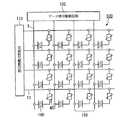
図1は、本実施の形態の液晶表示装置100についての等価回路を示している。この液晶表示装置100は、走査信号駆動回路110及びデータ信号駆動回路120を含んでいる。液晶表示装置100には、信号線、すなわち複数の走査線13と、該走査線13と交差する複数のデータ線9とが設けられ、走査線13は走査信号駆動回路110により、データ線9はデータ信号駆動回路120により駆動される。そして、各画素領域150において、走査線13とデータ線9との間にTFD素子40と液晶表示要素160(液晶層)とが直列に接続されている。なお、図1では、TFD素子40が走査線13側に接続され、液晶表示要素160がデータ線9側に接続されているが、これとは逆にTFD素子40をデータ線9側に、液晶表示要素160を走査線13側に設ける構成としても良い。[First Embodiment]
The liquid crystal display device of the present embodiment shown below is an example of an active matrix liquid crystal display device using a thin film diode (hereinafter abbreviated as TFD) as a switching element, and particularly reflective display and transmission. This is a transflective liquid crystal display device that enables display.
FIG. 1 shows an equivalent circuit for the liquid
次に、図2に基づいて、本実施の形態の液晶表示装置に具備された電極の平面構造について説明する。図2に示すように、本実施の形態の液晶表示装置では、走査線13にTFD素子40を介して接続された平面視矩形状の画素電極31がマトリクス状に設けられており、該画素電極31と紙面垂直方向に対向して共通電極9が短冊状(ストライプ状)に設けられている。共通電極9はデータ線からなり走査線13と交差する形のストライプ形状を有している。本実施の形態において、各画素電極31が形成された個々の領域が1つのドット領域であり、該マトリクス状に配置された各ドット領域毎に表示が可能な構造になっている。 Next, the planar structure of the electrodes provided in the liquid crystal display device of the present embodiment will be described with reference to FIG. As shown in FIG. 2, in the liquid crystal display device of the present embodiment,
ここでTFD素子40は走査線13と画素電極31とを接続するスイッチング素子であって、TFD素子40は、Taを主成分とする第1導電膜と、第1導電膜の表面に形成され、Ta2O3を主成分とする絶縁膜と、絶縁膜の表面に形成され、Crを主成分とする第2導電膜とを含むMIM構造を具備して構成されている。そして、TFD素子40の第1導電膜が走査線13に接続され、第2導電膜が画素電極31に接続されている。Here, the
次に、図3に基づいて本実施の形態の液晶表示装置100の画素構成について説明する。図3(a)は、液晶表示装置100の画素構成、特に画素電極31の平面構成を示す模式図、図3(b)は図3(a)のA−A’断面を示す模式図である。本実施の形態の液晶表示装置100は、図2に示したようにデータ線9及び走査線13等にて囲まれた領域の内側に画素電極31を備えてなるドット領域を有している。このドット領域内には、図3(a)に示すように一のドット領域に対応して3原色のうちの一の着色層が配設され、3つのドット領域(D1,D2,D3)で各着色層22B(青色),22G(緑色),22R(赤色)を含む画素を形成している。 Next, the pixel configuration of the liquid
一方、図3(b)に示すように、本実施の形態の液晶表示装置100は、上基板(素子基板)25とこれに対向配置された下基板(対向基板)10との間に初期配向状態が垂直配向をとる液晶、すなわち誘電異方性が負の液晶材料からなる液晶層50が挟持されている。
下基板10は、石英、ガラス等の透光性材料からなる基板本体10Aの表面にアルミニウム、銀等の反射率の高い金属膜からなる反射膜20が絶縁膜24を介して部分的に形成された構成をなしている。ここで、反射膜20の形成領域が反射表示領域Rとなり、反射膜20の非形成領域、すなわち反射膜20の開口部21内が透過表示領域Tとなる。このように本実施の形態の液晶表示装置は、垂直配向型の液晶層50を備える垂直配向型液晶表示装置であって、反射表示及び透過表示を可能にした半透過反射型の液晶表示装置である。On the other hand, as shown in FIG. 3B, the liquid
In the
基板本体10A上に形成された絶縁膜24は、その表面に凹凸形状24aを具備してなり、その凹凸形状24aに倣って反射膜20の表面は凹凸部を有する。このような凹凸により反射光が散乱されるため、外部からの映り込みが防止され、広視野角の表示を得ることが可能とされている。 The insulating
また、反射表示領域R内に位置する反射膜20上、及び透過表示領域T内に位置する基板本体10A上には、これら反射表示領域R及び透過表示領域Tに跨って形成されるカラーフィルタ22(図3(b)では赤色着色層22R)が設けられている。ここで、着色層22Rの周縁は金属クロム等からなるブラックマトリクスBMにて囲まれ、ブラックマトリクスBMにより各ドット領域D1,D2、D3の境界が形成されている(図3(a)参照)。 Further, the
さらに、このカラーフィルタ22上には、反射表示領域Rに対応する位置に絶縁膜26が形成されている。すなわち、カラーフィルタ22を介して反射膜20の上方に位置するように選択的に絶縁膜26が形成され、該絶縁膜26の形成に伴って液晶層50の層厚を反射表示領域Rと透過表示領域Tとで異ならしめている。絶縁膜26は例えば膜厚が0.5〜2.5μm程度のアクリル樹脂等の有機膜からなり、反射表示領域Rと透過表示領域Tとの境界付近において、自身の層厚が連続的に変化するべく傾斜面を備えている。絶縁膜26が存在しない部分の液晶層50の厚みが1〜5μm程度とされ、反射表示領域Rにおける液晶層50の厚みは透過表示領域Tにおける液晶層50の厚みの約半分とされている。 Further, an insulating
このように絶縁膜26は、自身の膜厚によって反射表示領域Rと透過表示領域Tとの液晶層50の層厚を異ならせる液晶層厚調整層(液晶層厚制御層)として機能するものである。また、本実施の形態の場合、絶縁膜26の上部の平坦面の縁と反射膜20(反射表示領域)の縁とが略一致しており、絶縁膜26の傾斜領域の一部又は全部が透過表示領域Tに含まれることになる。 Thus, the insulating
そして、絶縁膜26の表面を含む下基板10の表面には、インジウム錫酸化物(Indium Tin Oxide, 以下、ITOと略記する)からなる共通電極9が形成され、共通電極9上にはポリイミド等からなる配向膜27が形成されている。配向膜27は液晶分子を膜面に対して垂直に配向させる垂直配向膜として機能するものであって、ラビングなどの配向処理は施されていない。なお、図3において共通電極9は、紙面垂直方向に延びる形のストライプ状に形成されており、該紙面垂直方向に並んで形成されたドット領域の各々に共通の電極として構成されるとともに、共通電極9には該電極の一部を部分的に切り欠いた形状のスリット91が形成されている。さらに、本実施の形態では、反射膜20と共通電極9とを別個に設けて積層したが、反射表示領域Rにおいては金属膜からなる反射膜を共通電極の一部として用いることも可能である。 A
次に、上基板25側においては、ガラスや石英等の透光性材料からなる基板本体25A上(基板本体25Aの液晶層側)に、ITO等の透明導電膜からなるマトリクス状の画素電極31が形成されている。また、画素電極31上には誘電体からなる突起(凸状部)28,29が形成されており、具体的には、画素電極31の内面側(液晶層側)であって、透過表示領域T及び反射表示領域Rの双方において、それぞれ突起28,29が形成されている。さらに、突起28,29を含む画素電極31上にはポリイミド等からなる下基板10と同様の垂直配向処理された配向膜33とが形成されている。 Next, on the
次に、下基板10の外面側(液晶層50を挟持する面とは異なる側)には位相差板18及び偏光板19が、上基板25の外面側にも位相差板16及び偏光板17が形成されており、基板内面側(液晶層50側)に円偏光を入射可能に構成されており、これら位相差板18及び偏光板19、位相差板16及び偏光板17が、それぞれ円偏光板を構成している。偏光板17(19)は、所定方向の偏光軸を備えた直線偏光のみを透過させる構成とされ、位相差板16(18)としてはλ/4位相差板が採用されている。なお、下基板10に形成された偏光板19の外側には透過表示用の光源たるバックライト15が設けられている。 Next, the
ここで、本実施の形態の液晶表示装置100においては、液晶層50の液晶分子を配向規制するために、つまり初期状態において垂直配向にある液晶分子について、電極間に電圧を印加した際の傾倒方向を規制する手段として、上述したように電極の内面側(液晶層側)に誘電体からなる突起28,29が形成されている。図3の例においては、上基板25の内面側に形成された画素電極31の内面側(液晶層側)に、透過表示領域T及び反射表示領域Rの双方においてそれぞれ突起28,29が形成されている。 Here, in the liquid
各突起28,29は、上基板25の内面(電極主面)から液晶層50の内部に突出する形にて円錐状若しくは多角錘状に構成され、基板内面(電極主面)に対して所定の角度で傾斜する傾斜面(緩やかに湾曲した形状を含む)を少なくとも備え、該傾斜面に沿って液晶分子LCの傾倒方向を規制するものとされている。 Each of the
一方、下基板10の内面側に形成された共通電極9には、該電極の一部を部分的に切り欠いた形状のスリット91が形成されている。該スリット91を設けたことにより、該スリット形成領域において各電極9,31間に斜め電界が生じ、該斜め電界に応じて、初期状態で垂直配向した液晶分子の電圧印加に基づく傾倒方向が規制されることとなる。なお、図3(a)に示すように、共通電極9に形成されたスリット91は、画素電極31に形成された突起28,29を取り囲む形にて構成されており、その結果、突起28,29の周りに沿って液晶分子LCの傾倒方向を放射状に規制することが可能となる。 On the other hand, the
以上のような構成の液晶表示装置100によれば、以下のような効果を発現することができるようになる。
つまり、一般的には、ラビング処理を施さない垂直配向膜上に配向した負の誘電異方性を有する液晶分子に電圧を印加すると、液晶の倒れる方向に規制がないので無秩序な方向に倒れ、配向不良が生じることとなる。しかしながら、本実施の形態では、画素電極31の内面側に突起28,29を形成し、さらにその突起28,29を平面的に観て取り囲む形にて共通電極9にスリット91を形成したため、突起28,29の傾斜面による配向規制、及び/又はスリット91に基づく斜め電界による配向規制が生じ、初期状態で垂直配向した液晶分子の、電圧印加により倒れる方向が規制されることとなる。その結果、液晶配向不良に基づくディスクリネーションの発生が抑制されるため、ディスクリネーションの発生に伴う残像や斜め方向から観察したときのざらざらとしたしみ状のムラ等が発生し難い高品質な表示が得られる。According to the liquid
That is, in general, when a voltage is applied to liquid crystal molecules having negative dielectric anisotropy aligned on a vertical alignment film that is not subjected to rubbing treatment, there is no restriction on the direction in which the liquid crystal falls, so it falls in a disorderly direction, An orientation failure will occur. However, in the present embodiment, since the
また、本実施形態の液晶表示装置100では、反射表示領域Rに絶縁膜26を設けたことによってマルチギャップ構造を実現でき、すなわち反射表示領域Rの液晶層50の厚みを透過表示領域Tの液晶層50の厚みの略半分と小さくすることができるので、反射表示に寄与するリタデーションと透過表示に寄与するリタデーションを略等しくすることができ、これによりコントラストの向上が図られている。 Further, in the liquid
そして、マルチギャップ構造を実現するために形成した絶縁膜26を備えた下基板10ではなく、上基板25側に突起28,29を形成するものとしたために、該突起28,29の形成及び該突起28,29の高さ設計を容易に行うことができるようになっている。すなわち、絶縁膜26を形成した下基板10の液晶層50側表面は、マルチギャップ構造に相応する段差が形成されており、その段差の凹部に突起28,29を形成するには非常に手間が掛かり、また段差の影響で凹部と凸部とで形成する突起28,29の高さに違いが生じる場合もある。しかしながら、本実施形態のように絶縁膜26を備える基板と異なる基板側に突起28,29を形成した場合には、相対的に平坦な面上に突起28,29を形成することができるため、上記製造上の問題が生じ難く、非常に簡便に突起28,29を形成することが可能となり、またその高さ設計も非常に容易に行うことが可能となるのである。 Since the
なお、突起28,29について、透過表示領域Tの突起28の突出高さが相対的に大きく構成されたものとすることもできる。マルチギャップ構造の採用により透過表示領域Tの液晶層厚が相対的に大きく形成されているため、透過表示領域Tにおいては一層大きな配向規制力が必要であり、上記のように突出高さを設計するのが好ましい。 Note that the
[第2の実施の形態]
次に、第2の実施の形態の液晶表示装置について、図面を参照しつつ説明する。図4は、第2の実施の形態の液晶表示装置200について、その平面構造(a)及び断面構造(b)を示す模式図であって、第1の実施の形態の図3に相当する図面である。本第2の実施の形態の液晶表示装置200は、カラーフィルタの構成が主として異なる以外は、図3に示した液晶表示装置100と基本構造は略同様であり、したがって図3に付した符号と同一符号のものについては、特に記述がない限り同一の構成部材として説明を省略するものとする。[Second Embodiment]
Next, a liquid crystal display device according to a second embodiment will be described with reference to the drawings. FIG. 4 is a schematic diagram showing a planar structure (a) and a cross-sectional structure (b) of the liquid
第2の実施の形態の液晶表示装置200は、スイッチング素子としてTFDを用いたアクティブマトリクス型の半透過反射型液晶表示装置の例であって、上基板(素子基板)25とこれに対向配置された下基板(対向基板)10との間に初期配向状態が垂直配向をとる液晶、すなわち誘電異方性が負の液晶材料からなる液晶層50が挟持されている。 The liquid
下基板10は、石英、ガラス等の透光性材料からなる基板本体10Aの表面にアルミニウム、銀等の反射率の高い金属膜からなる反射膜20が所定パターンにて、具体的には反射表示領域Rに選択的に形成されている。なお、第1の実施の形態と同様に、絶縁膜24を介して凹凸形状を付与することも可能である。 The
このように反射表示領域Rに選択的に形成された反射膜20上、及び透過表示領域T内に位置する基板本体10A上には、これら反射表示領域R及び透過表示領域Tに跨って形成されるカラーフィルタ22(22R,22G,22B)が設けられている。カラーフィルタ22は赤色、緑色、青色の各色着色層22R,22G,22Bを備えてなり、各色着色層22R,22G,22Bが各ドット領域D1,D2、D3を形成している(図4(a)参照)。 In this way, on the
本実施形態では、各ドット領域D1,D2、D3の境界領域に形成されるブラックマトリクスBMが従来汎用されている金属クロムではなく、各色の着色層22R,22G,22Bの積層体にて構成されている。具体的には、反射表示領域Rに隣接するドット間領域において、各色の着色層22R,22G,22Bが平面的に重なって形成されており、その積層体により黒が表示される構成となっている。なお、このように各着色層を積層した結果、当該ドット間領域において、該積層分だけカラーフィルタ22の層厚が厚膜に形成されることとなる。 In the present embodiment, the black matrix BM formed in the boundary region between the dot regions D1, D2, and D3 is not a metal chrome conventionally used, but is formed of a stacked body of
さらに、このカラーフィルタ22上には、着色層22R,22G,22Bが重ねて形成された領域を覆う態様にて、反射表示領域Rに対応する位置に液晶層厚調整層たる絶縁膜26が形成されている。また、該絶縁膜26の表面を含む下基板10の表面にはITOからなる共通電極9が形成されおり、共通電極9上にはポリイミド等からなる垂直配向性の配向膜27が形成されている。なお、上述のように各着色層22R,22G,22Bを積層した結果、該積層した領域では積層分だけカラーフィルタ22が突出して形成されており、絶縁膜26にも該突出したカラーフィルタ22に倣って一部突出した部分が形成されている。また、共通電極9には該電極の一部を部分的に切り欠いた形状のスリット91が形成されている。 Further, an insulating
次に、上基板25側においては、ガラスや石英等の透光性材料からなる基板本体25A上(基板本体25Aの液晶層側)に、ITO等の透明導電膜からなるマトリクス状の画素電極31と、ポリイミド等からなる下基板10と同様の垂直配向処理された配向膜33とが形成されている。なお、第1の実施形態と同様に、画素電極31には該電極内面から液晶層50内部に突出する突起28が透過表示領域Tに形成されており、さらにドット間領域においても絶縁膜26が突出した領域に対応して、基板本体25A内面から液晶層50側に突出してなる突起29aが形成されている。この突起29aは、透過表示領域Tに形成された突起28と同一材料にて構成されており、突起28と略同一の高さにて構成されている。 Next, on the
このように、本実施の形態の液晶表示装置200においては、着色層22R,22G,22Bが重なって形成された領域であって、絶縁膜26を備えた下基板10とは異なる上基板25の液晶層50側には、基板本体25Aから液晶層50側に突出してなる突起29aが形成されており、これを液晶層50の層厚を規制する手段(スペーサーの代用)として用いている。つまり、上記着色層22R,22G,22Bが重ねて形成された領域は、その重ねられた分だけ、その他の領域よりも突出した形となっているが、この重ねられた着色層を覆う形にて絶縁層26を形成し、さらにこの領域に突起29aを形成した場合には、基板面内において該突起29aの形成領域の液晶層厚が最も突出してなるものとすることができ、その結果、突起29aを液晶層厚を規制する手段として用いることができたのである。したがって、別途スペーサーを配設することなく液晶層厚を面内均一に維持することが可能となる。なお、突起29aは、製造効率の向上を目的として、透過表示領域Tに形成された突起28と同一プロセスにて形成するものとされており、また、突起28と略同一の高さにて構成されている。 As described above, in the liquid
このような構成の液晶表示装置200によれば、第1の実施の形態の液晶表示装置100が具備する幾つかの効果を奏するに加えて、別途金属クロムを用いることなくブラックマトリクスBMを形成することができるため、製造効率が向上し、コスト削減を可能とするとともに、金属クロム等の廃棄による環境破壊の問題も回避することが可能となり得る。また、別途スペーサーを用いることなく液晶層厚を規制することが可能なため、製造効率が向上し、コスト削減が実現可能となる。さらに、下基板10側には絶縁膜26に加え、着色層22R,22G,22Bを重ねて形成したため、該下基板10に形成される段差は一層大きなものとなり得る。そこで、本実施の形態のように突起28,29aを上基板25側に形成することで、製造効率及び突起高さの設計の容易性を一層向上させることが可能となる。 According to the liquid
以上、第2の実施の形態の液晶表示装置について示したが、例えば図5のような構成を付加することもできる。つまり、上記実施の形態では透過表示領域Tのみに突起28を形成しているが、図5の液晶表示装置300では、反射表示領域Rに対しても液晶分子の配向方向を規制するための突起29bを形成している。該反射表示領域Rに形成した突起29bは、ドット間領域の突起29aと略同一の高さにて形成することが好ましく、この場合、突起29bが対向する基板の内面に接してしまう不具合を解消でき、その結果、液晶分子の配向規制を良好に行うことが可能となる。 Although the liquid crystal display device of the second embodiment has been described above, for example, a configuration as shown in FIG. 5 can be added. That is, in the above embodiment, the
[第3の実施の形態]
次に、第3の実施の形態の液晶表示装置について、図面を参照しつつ説明する。図6は、第3の実施の形態の液晶表示装置400について、その平面構造(a)及び断面構造(b)を示す模式図であって、第2の実施の形態の図4及び図5に相当する図面である。本第3の実施の形態の液晶表示装置400は、第2の実施の形態に比して、カラーフィルタ22(着色層22R,22G,22B)及び絶縁膜26が上基板25側に形成され、突起28,29a,29bが下基板10側に形成されている以外は、図4に示した液晶表示装置200及び図5に示した液晶表示装置300と基本構造は略同様であり、したがって図4及び図5に付した符号と同一符号のものについては、特に記述がない限り同一の構成部材として説明を省略するものとする。[Third Embodiment]
Next, a liquid crystal display device according to a third embodiment will be described with reference to the drawings. FIG. 6 is a schematic diagram showing a planar structure (a) and a cross-sectional structure (b) of the liquid
図6に示すように、第3実施の形態の液晶表示装置400は、スイッチング素子として薄膜トランジスタ(TFT)を用いたアクティブマトリクス型の半透過反射型液晶表示装置の例であって、下基板(素子基板)10とこれに対向配置された上基板(対向基板)25との間に初期配向状態が垂直配向をとる液晶、すなわち誘電異方性が負の液晶材料からなる液晶層50が挟持されている。 As shown in FIG. 6, the liquid
下基板10は、基板本体10Aの表面にアルミニウム、銀等の反射率の高い金属膜からなる反射膜20aが所定パターンにて、具体的には反射表示領域Rに選択的に形成されている。さらに、反射膜20aの形成されていない領域、すなわち透過表示領域Tには所定パターンの透明電極9aが形成され、これら反射膜20a及び透明電極9aが一対になってマトリクス状に形成された画素電極を構成している。 In the
そして、これら画素電極を構成する反射膜20a及び/又は透明電極9a上には、突起28,29a,29bが形成されており、それぞれ透過表示領域T、反射表示領域R、ドット間領域に位置してなるものである。これら突起28,29a,29bの構成については、上記第2の実施の形態と同様のものである。なお、突起28,29a,29bを含む反射膜20a及び透明電極9a上には垂直配向性の配向膜27が形成されている。
一方、上基板25は、基板本体25Aの表面に各色の着色層22R,22G,22Bが重ねて形成された領域を含むカラーフィルタ22が配設され、該カラーフィルタ22上には、液晶層厚調整層たる絶縁膜26と、全面ベタ状に形成された共通電極31aとが配設されている。なお、共通電極31aには、該電極を部分的に切り欠いたスリット91が形成されており、該スリット91において斜め電界が生じるものなっている。また、共通電極31a上には垂直配向性を有する配向膜33aが形成されている。 On the other hand, the
このように、本実施形態においても、画素電極の間に位置するカラーフィルタ22のドット間領域には、各着色層22R,22G,22Bが積層してなるブラックマトリクスBMが形成されている。具体的には、反射表示領域Rに隣接するドット間領域において、各色の着色層22R,22G,22Bが平面的に重なって形成されており、その積層体により黒が表示される構成となっている。なお、このように各着色層を積層した結果、当該ドット間領域において、該積層分だけカラーフィルタ22の層厚が厚膜に形成されることとなる。そして、突起29aが液晶層厚を規制する手段として機能し、一方、突起28,29bが液晶分子の倒れる方向を規制する手段として機能することとなる。 As described above, also in the present embodiment, the black matrix BM formed by laminating the
以上のように、各着色層22R,22G,22Bを積層してブラックマトリクスを構成したカラーフィルタ22を上基板25側に含む第3の実施の形態の液晶表示装置400によっても、第1の実施の形態の液晶表示装置100及び第2の実施の形態の液晶表示装置200,300が具備する幾つかの効果を奏することが可能となる。 As described above, the liquid
[第4の実施の形態]
次に、第4の実施の形態の液晶表示装置について、図面を参照しつつ説明する。図7は、第4の実施の形態の液晶表示装置500について、その平面構造(a)及び断面構造(b)を示す模式図であって、第2の実施の形態の図4及び図5に相当する図面である。本第4の実施の形態の液晶表示装置500は、液晶配向規制を目的として形成した突起の形状が主として異なる以外は、図4及び図5に示した液晶表示装置200,300と基本構造は略同様であり、したがって図4及び図5に付した符号と同一符号のものについては、特に記述がない限り同一の構成部材として説明を省略するものとする。[Fourth Embodiment]
Next, a liquid crystal display device according to a fourth embodiment will be described with reference to the drawings. FIG. 7 is a schematic diagram showing a planar structure (a) and a cross-sectional structure (b) of the liquid
図7に示すように、本実施形態の液晶表示装置500においては、表示領域であるドット領域に形成する液晶配向規制用の突起28,29bをライン状に形成した。つまり、第1〜第3の実施の形態では、円錐状ないし多角錘状の突起にて液晶分子の倒れる方向を規制したが、本実施の形態ではドット内で一方向に延びるライン状の突条にて液晶分子の倒れる方向を規制するものとしている。この場合、液晶分子の配向規制を一層良好に行うことが可能となる。 As shown in FIG. 7, in the liquid
[第5の実施の形態]
次に、第5の実施の形態の液晶表示装置について、図面を参照しつつ説明する。図9は、第5の実施の形態の液晶表示装置600について、その平面構造(a)及び断面構造(b)を示す模式図であって、第1の実施の形態の図3に相当する図面である。本第5の実施の形態の液晶表示装置600は、スイッチング素子及び画素電極の構成が主として異なる以外は、図3に示した液晶表示装置100と基本構造は略同様であり、したがって図3に付した符号と同一符号のものについては、特に記述がない限り同一の構成部材として説明を省略するものとする。[Fifth Embodiment]
Next, a liquid crystal display device according to a fifth embodiment will be described with reference to the drawings. FIG. 9 is a schematic diagram showing a planar structure (a) and a cross-sectional structure (b) of the liquid
第5の実施の形態の液晶表示装置600は、スイッチング素子としてTFT(薄膜トランジスタ)を用いたアクティブマトリクス型の半透過反射型液晶表示装置の例であって、下基板(素子基板)610とこれに対向配置された上基板(対向基板)625との間に初期配向状態が垂直配向をとる液晶、すなわち誘電異方性が負の液晶材料からなる液晶層50が挟持されている。 A liquid
下基板610は、石英、ガラス等の透光性材料からなる基板本体10Aを備え、その内面側には、第1の実施の形態と同様、反射表示領域Rに対応する位置に選択的に絶縁膜(液晶層厚調整層)26が形成されており、これに伴って液晶層50の層厚が反射表示領域Rと透過表示領域Tとで異なる構成となっている。なお、この絶縁膜26の内面側には、凹凸形状26aが付与されている。 The
次に、上記凹凸形状26aを備える絶縁膜26の内面側には、反射膜620が選択的に形成され、この反射膜620の形成領域が反射表示領域Rとなり、反射膜620の非形成領域、すなわち反射膜620の開口部内が透過表示領域Tとなる。なお、反射膜620は、絶縁膜26の凹凸形状26aに倣って凹凸を有し、反射表示における外部からの映り込みが防止され、広視野角の表示を得ることが可能とされている。 Next, a
一方、透過表示領域Tにおける基板本体10Aの内面側には、インジウム錫酸化物からなる電極609が形成されている。この電極609は、透過表示領域Tに選択的に形成され、反射表示領域Rの反射膜620と電気的に接続されている(図9(a)参照)。つまり、本実施の形態では、下基板610の内面側において、透過表示領域Tにはインジウム錫酸化物からなる電極609が配設されてなる一方、反射表示領域Rにはアルミニウム等の反射率の高い金属膜からなる反射膜620が配設されて、これら電極609と反射膜620とにより画素電極がマトリクス状に構成されている。なお、電極609及び反射膜620からなる画素電極には、透過表示領域Tの電極609にスリット91、電極609と反射膜620との境界部にスリット91がそれぞれ形成されている。 On the other hand, an
また、電極609及び反射膜620からなる画素電極609の内面側にはポリイミド等からなる配向膜27が形成されている。この配向膜27は液晶分子を膜面に対して垂直に配向させる垂直配向膜として機能するものであって、ラビングなどの配向処理は施されていない。 An
次に、上基板625は、石英、ガラス等の透光性材料からなる基板本体25Aを備え、その内面側にはカラーフィルタ22が形成され、さらにその内面側に、基板全面にベタ状に配設されてなる共通電極631が形成されている。また、共通電極631の内面側にはポリイミド等からなる配向膜33が形成されている。この配向膜33は液晶分子を膜面に対して垂直に配向させる垂直配向膜として機能するものであって、ラビングなどの配向処理は施されていない。 Next, the
ここで、共通電極631の内面側には、該電極内面から液晶層50内部に突出する突起28が透過表示領域Tに形成されており、具体的には、図9(a)に示すように、略矩形枠状の輪郭を有するスリット91の中央部に突起28が配設されている。なお、上基板625の基板本体25Aの内面側には、突起28と同時に形成したスペーサー(図示略)が画素領域外に配設されている。本実施の形態では、突起28とスペーサーの高さは略同じであるため、1度のフォト工程にて形成する樹脂等の誘電体からなる凸状部にて、これらを構成することができる。 Here, on the inner surface side of the
このように画素領域内の突起28は、電界印加時の液晶分子の傾倒方向を自身の傾斜面に沿って規制する配向制御手段として機能しており、画素領域外のスペーサーは液晶層厚(液晶セル厚)の制御手段として機能している。これにより、ディスクリネーションの発生、及び当該液晶表示装置を斜め方向から見たときに生じ得るざらざらとしたしみ状のムラの発生を防止ないし抑制することが可能となる。特に、本実施形態では、絶縁膜26を形成した基板と対向する基板側に複数の凸状部を形成し、画素領域においては液晶配向制御用の突起28として、画素領域外においては液晶層厚を制御するスペーサーとして用いており、製造効率の向上を実現している。なお、第2の実施の形態で示したように、突起28を反射表示領域Rに形成して、液晶分子の配向制御を行うことも可能である。 Thus, the
[電子機器]
次に、本発明の上記実施の形態の液晶表示装置を備えた電子機器の具体例について説明する。
図8は、携帯電話の一例を示した斜視図である。図8において、符号1000は携帯電話本体を示し、符号1001は上記液晶表示装置を用いた表示部を示している。このような電子機器は、上記実施の形態の液晶表示装置を用いた表示部を備えているので、使用環境によらずに明るく、コントラストが高く、広視野角の液晶表示部を備えた電子機器を実現することができる。[Electronics]
Next, specific examples of the electronic apparatus including the liquid crystal display device according to the above embodiment of the present invention will be described.
FIG. 8 is a perspective view showing an example of a mobile phone. In FIG. 8,
以上、本発明の実施の形態について、その一例を説明したが、本発明の技術範囲はこれらに限定されるものではなく、本発明の趣旨を逸脱しない範囲において種々の変更を加えることが可能である。例えば上記実施の形態では位相差板を単板で構成したが、この代わりに、1/2波長板と1/4波長板との積層体として構成してもよい。この積層体は広帯域円偏光板として機能し、黒表示をより無彩色化にすることができる。また、本実施の形態で形成した突起の形状、電極スリットの形状についても、上記実施の形態の構成に限られるものではなく、少なくとも垂直配向した液晶分子の傾倒方向を規制するための構成を具備していれば良い。 As mentioned above, although the example was demonstrated about embodiment of this invention, the technical scope of this invention is not limited to these, A various change can be added in the range which does not deviate from the meaning of this invention. is there. For example, in the above-described embodiment, the retardation plate is configured as a single plate, but instead, it may be configured as a laminated body of a ½ wavelength plate and a ¼ wavelength plate. This laminated body functions as a broadband circularly polarizing plate, and the black display can be made more achromatic. Further, the shape of the protrusions and the shape of the electrode slits formed in this embodiment are not limited to the configuration in the above embodiment, and at least have a configuration for regulating the tilt direction of vertically aligned liquid crystal molecules. If you do.
9…共通電極、20…反射膜、26…絶縁膜(液晶層厚調整層)、28,29…突起、31…画素電極、50…液晶層、R…反射表示領域、T…透過表示領域 DESCRIPTION OF
Claims (12)
Translated fromJapanese前記液晶層は、誘電異方性が負の液晶からなり、
前記一対の基板のうちの少なくとも一方の基板と前記液晶層との間には、前記反射表示領域の液晶層厚を前記透過表示領域の液晶層厚よりも小さくするための液晶層厚調整層が設けられ、
前記一対の基板の前記液晶層側には該液晶を駆動するための電極がそれぞれ設けられ、
さらに前記液晶層厚調整層が形成された基板とは異なる基板において、前記透過表示領域及び前記反射表示領域のそれぞれにおいて、該基板内面から前記液晶層内部に突出する凸状部が設けられ、
前記凸状部及び前記電極の液晶層側に、前記液晶を垂直配向させる配向膜が形成されていることを特徴とする液晶表示装置。A liquid crystal display device in which a liquid crystal layer is sandwiched between a pair of substrates, and a transmissive display region and a reflective display region are provided in one dot region,
The liquid crystal layer is made of a liquid crystal having negative dielectric anisotropy,
Between the liquid crystal layer and at least one of the pair of substrates, there is a liquid crystal layer thickness adjusting layer for making the liquid crystal layer thickness of the reflective display region smaller than the liquid crystal layer thickness of the transmissive display region. Provided,
Electrodes for driving the liquid crystal are provided on the liquid crystal layer side of the pair of substrates,
Furthermore, in a substrate different from the substrate on which the liquid crystal layer thickness adjusting layer is formed, a convex portion protruding from the substrate inner surface to the inside of the liquid crystal layer is provided in each of the transmissive display region and the reflective display region,
An alignment film for vertically aligning the liquid crystal is formed on the convex portion and the liquid crystal layer side of the electrode.
前記液晶層厚調整層が設けられた基板の電極には、前記液晶層厚調整層の前記傾斜面において前記電極を部分的に切り欠いた形状のスリットが設けられていることを特徴とする請求項1ないし4のいずれか1項に記載の液晶表示装置。The liquid crystal layer thickness adjusting layer has an inclined surface between the transmissive display area and the reflective display area,
The electrode of the substrate provided with the liquid crystal layer thickness adjusting layer is provided with a slit having a shape in which the electrode is partially cut out on the inclined surface of the liquid crystal layer thickness adjusting layer. Item 5. The liquid crystal display device according to any one of Items 1 to 4.
前記液晶層は、誘電異方性が負の液晶からなり、
前記一対の基板のうちの少なくとも一方の基板と前記液晶層との間には、前記反射表示領域の液晶層厚を前記透過表示領域の液晶層厚よりも小さくするための液晶層厚調整層が設けられ、
さらに前記液晶層厚調整層が形成された基板とは異なる基板において、該基板内面から前記液晶層内部に突出する第1凸状部が設けられ、
前記第1凸状部及び前記電極の液晶層側に、前記液晶を垂直配向させる配向膜が形成され、
前記液晶層厚調整層が形成された基板側にカラーフィルタ層が設けられ、該カラーフィルタ層は複数の着色層を備えてなり、該複数の着色層がドット間領域において平面的に重なって形成され、
前記カラーフィルタ層の液晶層側には、少なくとも前記着色層が重なって形成された領域を覆う形にて前記液晶層厚調整層が形成され、
さらに前記カラーフィルタ層及び前記液晶層厚調整層が形成された基板とは異なる基板には、少なくとも前記着色層が重なって形成された領域と対向する領域に該基板から前記液晶層側に突出してなる第2凸状部が形成されていることを特徴とする液晶表示装置。A liquid crystal display device in which a liquid crystal layer is sandwiched between a pair of substrates, and a transmissive display region and a reflective display region are provided in one dot region,
The liquid crystal layer is made of a liquid crystal having negative dielectric anisotropy,
Between the liquid crystal layer and at least one of the pair of substrates, there is a liquid crystal layer thickness adjusting layer for making the liquid crystal layer thickness of the reflective display region smaller than the liquid crystal layer thickness of the transmissive display region. Provided,
Furthermore, in a substrate different from the substrate on which the liquid crystal layer thickness adjusting layer is formed, a first convex portion protruding from the substrate inner surface into the liquid crystal layer is provided,
An alignment film for vertically aligning the liquid crystal is formed on the liquid crystal layer side of the first convex portion and the electrode,
A color filter layer is provided on the substrate side on which the liquid crystal layer thickness adjusting layer is formed, the color filter layer includes a plurality of colored layers, and the plurality of colored layers are formed to overlap in a region between dots in a plane. And
The liquid crystal layer thickness adjusting layer is formed on the liquid crystal layer side of the color filter layer so as to cover at least a region formed by overlapping the colored layers,
Further, the substrate different from the substrate on which the color filter layer and the liquid crystal layer thickness adjusting layer are formed protrudes from the substrate to the liquid crystal layer side at least in a region facing the region where the colored layer is overlapped. The liquid crystal display device is characterized in that a second convex portion is formed.
Priority Applications (6)
| Application Number | Priority Date | Filing Date | Title |
|---|---|---|---|
| JP2004031056AJP3807405B2 (en) | 2003-06-06 | 2004-02-06 | Liquid crystal display device and electronic device |
| US10/842,423US7277146B2 (en) | 2003-06-06 | 2004-05-11 | Vertical alignment mode LCD with larger dielectric protrusions in transmissive region than in reflection region |
| TW093114476ATWI284216B (en) | 2003-06-06 | 2004-05-21 | LCD device and electronic machine |
| KR1020040040759AKR100630020B1 (en) | 2003-06-06 | 2004-06-04 | Liquid crystal display device and electronic apparatus |
| CN200410042948XACN1573429B (en) | 2003-06-06 | 2004-06-04 | Liquid crystal display device and electronic equipment |
| US11/892,749US7471363B2 (en) | 2003-06-06 | 2007-08-27 | Vertical alignment model LCD with larger dielectric protrusions in transmissive region than in reflection region |
Applications Claiming Priority (2)
| Application Number | Priority Date | Filing Date | Title |
|---|---|---|---|
| JP2003162355 | 2003-06-06 | ||
| JP2004031056AJP3807405B2 (en) | 2003-06-06 | 2004-02-06 | Liquid crystal display device and electronic device |
Publications (2)
| Publication Number | Publication Date |
|---|---|
| JP2005018028A JP2005018028A (en) | 2005-01-20 |
| JP3807405B2true JP3807405B2 (en) | 2006-08-09 |
Family
ID=34117871
Family Applications (1)
| Application Number | Title | Priority Date | Filing Date |
|---|---|---|---|
| JP2004031056AExpired - LifetimeJP3807405B2 (en) | 2003-06-06 | 2004-02-06 | Liquid crystal display device and electronic device |
Country Status (5)
| Country | Link |
|---|---|
| US (2) | US7277146B2 (en) |
| JP (1) | JP3807405B2 (en) |
| KR (1) | KR100630020B1 (en) |
| CN (1) | CN1573429B (en) |
| TW (1) | TWI284216B (en) |
Families Citing this family (24)
| Publication number | Priority date | Publication date | Assignee | Title |
|---|---|---|---|---|
| JP4165337B2 (en)* | 2003-08-18 | 2008-10-15 | セイコーエプソン株式会社 | Liquid crystal display device and electronic device |
| US7532280B2 (en)* | 2004-07-20 | 2009-05-12 | Sharp Kabushiki Kaisha | Liquid crystal display device |
| JP4541815B2 (en)* | 2004-09-22 | 2010-09-08 | シャープ株式会社 | Transflective liquid crystal display device and manufacturing method thereof |
| JP4600076B2 (en)* | 2005-02-18 | 2010-12-15 | エプソンイメージングデバイス株式会社 | Liquid crystal device and electronic device |
| JP4082418B2 (en) | 2005-03-04 | 2008-04-30 | エプソンイメージングデバイス株式会社 | Liquid crystal device and electronic device |
| KR20060100868A (en)* | 2005-03-18 | 2006-09-21 | 삼성전자주식회사 | Liquid crystal display |
| US7995170B2 (en) | 2005-03-23 | 2011-08-09 | Sharp Kabushiki Kaisha | Liquid crystal display device |
| KR20060118153A (en)* | 2005-05-16 | 2006-11-23 | 삼성전자주식회사 | Semi-transmissive liquid crystal display device, display panel for this and manufacturing method thereof |
| JP2006330602A (en)* | 2005-05-30 | 2006-12-07 | Sharp Corp | Liquid crystal display device and manufacturing method thereof |
| JP4926063B2 (en)* | 2005-08-03 | 2012-05-09 | シャープ株式会社 | Liquid crystal display device and electronic apparatus including the same |
| JP4684808B2 (en)* | 2005-08-29 | 2011-05-18 | 株式会社 日立ディスプレイズ | Liquid crystal display device and information terminal device including the same |
| EP1777578B1 (en)* | 2005-10-18 | 2008-12-24 | Semiconductor Energy Laboratory Co., Ltd. | Liquid crystal display device and electronic apparatus |
| JP4663613B2 (en)* | 2005-10-18 | 2011-04-06 | 株式会社半導体エネルギー研究所 | Liquid crystal display device |
| JP4766673B2 (en)* | 2005-11-29 | 2011-09-07 | カシオ計算機株式会社 | Liquid crystal display element |
| JP4600265B2 (en)* | 2005-12-12 | 2010-12-15 | ソニー株式会社 | Liquid crystal device and electronic device |
| US7978298B2 (en)* | 2006-03-23 | 2011-07-12 | Sharp Kabushiki Kaisha | Liquid crystal display device |
| JP2007256843A (en)* | 2006-03-24 | 2007-10-04 | Toshiba Matsushita Display Technology Co Ltd | Liquid crystal display device |
| US8111356B2 (en)* | 2006-09-12 | 2012-02-07 | Sharp Kabushiki Kaisha | Liquid crystal display panel provided with microlens array, method for manufacturing the liquid crystal display panel, and liquid crystal display device |
| JP4865801B2 (en) | 2006-09-28 | 2012-02-01 | シャープ株式会社 | Liquid crystal display panel with microlens array, manufacturing method thereof, and liquid crystal display device |
| US8068201B2 (en) | 2006-12-18 | 2011-11-29 | Sharp Kabushiki Kaisha | Liquid crystal display having particular auxiliary electrode |
| WO2008084589A1 (en) | 2007-01-11 | 2008-07-17 | Sharp Kabushiki Kaisha | Liquid crystal display panel with micro-lens array and liquid crystal display device |
| JP5077367B2 (en)* | 2010-01-28 | 2012-11-21 | 凸版印刷株式会社 | Color filter substrate for transflective liquid crystal display device, manufacturing method thereof, and transflective liquid crystal display device |
| KR20140046239A (en)* | 2012-10-10 | 2014-04-18 | 삼성디스플레이 주식회사 | Liquid crystal display and manufacturing method thereof |
| TWI860119B (en)* | 2023-10-06 | 2024-10-21 | 凌巨科技股份有限公司 | Vertical alignment liquid crystal display panel structure |
Family Cites Families (23)
| Publication number | Priority date | Publication date | Assignee | Title |
|---|---|---|---|---|
| JPH03164733A (en)* | 1989-11-24 | 1991-07-16 | Fuji Photo Film Co Ltd | Image forming method |
| JPH09120062A (en)* | 1995-08-18 | 1997-05-06 | Toshiba Electron Eng Corp | Color filter substrate, manufacturing method thereof, liquid crystal display device using the same, and manufacturing method thereof |
| JPH1039318A (en) | 1996-07-24 | 1998-02-13 | Toshiba Corp | Liquid crystal display device |
| TW509808B (en) | 1997-06-12 | 2002-11-11 | Sharp Kk | Liquid crystal display device |
| US6281952B1 (en) | 1997-12-26 | 2001-08-28 | Sharp Kabushiki Kaisha | Liquid crystal display |
| JP3255107B2 (en) | 1998-02-27 | 2002-02-12 | 東レ株式会社 | Color filter and liquid crystal display device using the same |
| DE60005760D1 (en)* | 1999-02-15 | 2003-11-13 | Citizen Watch Co Ltd | LIQUID CRYSTAL DISPLAY |
| JP2000267081A (en) | 1999-03-17 | 2000-09-29 | Toshiba Corp | Liquid crystal display |
| US6906768B1 (en)* | 1999-11-24 | 2005-06-14 | Lg.Philips Lcd Co., Ltd. | Multi-domain liquid crystal display device with particular dielectric structures |
| JP2001183648A (en)* | 1999-12-24 | 2001-07-06 | Nec Corp | Color liquid crystal display device and method of producing the same |
| US6924876B2 (en)* | 2000-02-25 | 2005-08-02 | Sharp Kabushiki Kaisha | Liquid crystal display device |
| JP3656734B2 (en)* | 2000-03-17 | 2005-06-08 | シャープ株式会社 | Liquid crystal display |
| JP2001343660A (en)* | 2000-03-31 | 2001-12-14 | Sharp Corp | Liquid crystal display device and defect repair method thereof |
| JP2002182036A (en)* | 2000-04-06 | 2002-06-26 | Fujitsu Ltd | Viewing angle compensation film and liquid crystal display device |
| JP3712637B2 (en)* | 2000-08-11 | 2005-11-02 | シャープ株式会社 | Liquid crystal display device and defect correcting method thereof |
| JP2002091097A (en)* | 2000-09-13 | 2002-03-27 | Canon Inc | Image forming apparatus and process cartridge |
| TW548456B (en)* | 2000-12-29 | 2003-08-21 | Ind Tech Res Inst | Continuous domain inversed TN LCD device and the fabrication method thereof |
| SG160191A1 (en)* | 2001-02-28 | 2010-04-29 | Semiconductor Energy Lab | Semiconductor device and manufacturing method thereof |
| JP3875125B2 (en)* | 2001-04-11 | 2007-01-31 | シャープ株式会社 | Liquid crystal display |
| JP3767419B2 (en) | 2001-05-28 | 2006-04-19 | ソニー株式会社 | Liquid crystal display element |
| JP3675404B2 (en) | 2001-09-25 | 2005-07-27 | セイコーエプソン株式会社 | Transflective liquid crystal device and electronic equipment using the same |
| JP2003131205A (en) | 2001-10-26 | 2003-05-08 | Optrex Corp | Liquid crystal display panel and method for manufacturing the same |
| JP4039232B2 (en) | 2002-12-20 | 2008-01-30 | セイコーエプソン株式会社 | Liquid crystal display device and electronic device |
- 2004
- 2004-02-06JPJP2004031056Apatent/JP3807405B2/ennot_activeExpired - Lifetime
- 2004-05-11USUS10/842,423patent/US7277146B2/ennot_activeExpired - Lifetime
- 2004-05-21TWTW093114476Apatent/TWI284216B/ennot_activeIP Right Cessation
- 2004-06-04CNCN200410042948XApatent/CN1573429B/ennot_activeExpired - Lifetime
- 2004-06-04KRKR1020040040759Apatent/KR100630020B1/ennot_activeExpired - Lifetime
- 2007
- 2007-08-27USUS11/892,749patent/US7471363B2/ennot_activeExpired - Lifetime
Also Published As
| Publication number | Publication date |
|---|---|
| US7277146B2 (en) | 2007-10-02 |
| US20050030453A1 (en) | 2005-02-10 |
| US20080062365A1 (en) | 2008-03-13 |
| JP2005018028A (en) | 2005-01-20 |
| KR20040108614A (en) | 2004-12-24 |
| CN1573429A (en) | 2005-02-02 |
| TW200428072A (en) | 2004-12-16 |
| TWI284216B (en) | 2007-07-21 |
| CN1573429B (en) | 2010-05-26 |
| US7471363B2 (en) | 2008-12-30 |
| KR100630020B1 (en) | 2006-09-27 |
Similar Documents
| Publication | Publication Date | Title |
|---|---|---|
| JP3778179B2 (en) | Liquid crystal display device, method for manufacturing liquid crystal display device, electronic device | |
| JP3807405B2 (en) | Liquid crystal display device and electronic device | |
| US7403246B2 (en) | Liquid crystal display device and electronic apparatus | |
| JP3849659B2 (en) | Liquid crystal display device and electronic device | |
| JP3901172B2 (en) | Liquid crystal display device and electronic device | |
| JP4432371B2 (en) | Liquid crystal display device and electronic device | |
| JP3903980B2 (en) | Liquid crystal display device and electronic device | |
| JP3873962B2 (en) | Liquid crystal display device and electronic device | |
| JP4525259B2 (en) | Liquid crystal display device and electronic device | |
| JP4407234B2 (en) | Liquid crystal display device and electronic device | |
| JP4314906B2 (en) | Liquid crystal display device and electronic device | |
| JP4419502B2 (en) | Liquid crystal display device and electronic device | |
| JP2005128233A (en) | Liquid crystal display device and electronic device | |
| JP4249776B2 (en) | Liquid crystal display device and electronic device | |
| JP4513794B2 (en) | Liquid crystal display | |
| JP4618188B2 (en) | Liquid crystal display device and electronic device | |
| JP2007052455A (en) | Liquid crystal display device and electronic device | |
| JP2007034331A (en) | Manufacturing method of liquid crystal display device | |
| JP2005165191A (en) | Liquid crystal display device and electronic device | |
| JP2005055708A (en) | Liquid crystal display device and electronic device |
Legal Events
| Date | Code | Title | Description |
|---|---|---|---|
| A977 | Report on retrieval | Free format text:JAPANESE INTERMEDIATE CODE: A971007 Effective date:20051117 | |
| A131 | Notification of reasons for refusal | Free format text:JAPANESE INTERMEDIATE CODE: A131 Effective date:20051122 | |
| A521 | Request for written amendment filed | Free format text:JAPANESE INTERMEDIATE CODE: A523 Effective date:20060119 | |
| TRDD | Decision of grant or rejection written | ||
| A01 | Written decision to grant a patent or to grant a registration (utility model) | Free format text:JAPANESE INTERMEDIATE CODE: A01 Effective date:20060425 | |
| A61 | First payment of annual fees (during grant procedure) | Free format text:JAPANESE INTERMEDIATE CODE: A61 Effective date:20060508 | |
| R150 | Certificate of patent or registration of utility model | Free format text:JAPANESE INTERMEDIATE CODE: R150 Ref document number:3807405 Country of ref document:JP Free format text:JAPANESE INTERMEDIATE CODE: R150 | |
| FPAY | Renewal fee payment (event date is renewal date of database) | Free format text:PAYMENT UNTIL: 20100526 Year of fee payment:4 | |
| FPAY | Renewal fee payment (event date is renewal date of database) | Free format text:PAYMENT UNTIL: 20110526 Year of fee payment:5 | |
| FPAY | Renewal fee payment (event date is renewal date of database) | Free format text:PAYMENT UNTIL: 20120526 Year of fee payment:6 | |
| FPAY | Renewal fee payment (event date is renewal date of database) | Free format text:PAYMENT UNTIL: 20130526 Year of fee payment:7 | |
| FPAY | Renewal fee payment (event date is renewal date of database) | Free format text:PAYMENT UNTIL: 20140526 Year of fee payment:8 | |
| S111 | Request for change of ownership or part of ownership | Free format text:JAPANESE INTERMEDIATE CODE: R313113 | |
| S111 | Request for change of ownership or part of ownership | Free format text:JAPANESE INTERMEDIATE CODE: R313113 | |
| R371 | Transfer withdrawn | Free format text:JAPANESE INTERMEDIATE CODE: R371 | |
| S111 | Request for change of ownership or part of ownership | Free format text:JAPANESE INTERMEDIATE CODE: R313113 | |
| R350 | Written notification of registration of transfer | Free format text:JAPANESE INTERMEDIATE CODE: R350 | |
| R250 | Receipt of annual fees | Free format text:JAPANESE INTERMEDIATE CODE: R250 | |
| R250 | Receipt of annual fees | Free format text:JAPANESE INTERMEDIATE CODE: R250 | |
| R250 | Receipt of annual fees | Free format text:JAPANESE INTERMEDIATE CODE: R250 | |
| R250 | Receipt of annual fees | Free format text:JAPANESE INTERMEDIATE CODE: R250 | |
| R250 | Receipt of annual fees | Free format text:JAPANESE INTERMEDIATE CODE: R250 | |
| R250 | Receipt of annual fees | Free format text:JAPANESE INTERMEDIATE CODE: R250 | |
| R250 | Receipt of annual fees | Free format text:JAPANESE INTERMEDIATE CODE: R250 | |
| R250 | Receipt of annual fees | Free format text:JAPANESE INTERMEDIATE CODE: R250 | |
| EXPY | Cancellation because of completion of term |