JP3804878B2 - Dual-polarized antenna - Google Patents
Dual-polarized antennaDownload PDFInfo
- Publication number
- JP3804878B2 JP3804878B2JP05069297AJP5069297AJP3804878B2JP 3804878 B2JP3804878 B2JP 3804878B2JP 05069297 AJP05069297 AJP 05069297AJP 5069297 AJP5069297 AJP 5069297AJP 3804878 B2JP3804878 B2JP 3804878B2
- Authority
- JP
- Japan
- Prior art keywords
- conductor
- linear
- dual
- polarized antenna
- loop
- Prior art date
- Legal status (The legal status is an assumption and is not a legal conclusion. Google has not performed a legal analysis and makes no representation as to the accuracy of the status listed.)
- Expired - Fee Related
Links
- 239000004020conductorSubstances0.000claimsdescription146
- 239000000758substrateSubstances0.000claimsdescription23
- 230000003071parasitic effectEffects0.000claimsdescription9
- 238000006243chemical reactionMethods0.000claimsdescription6
- 230000005284excitationEffects0.000description18
- 230000010287polarizationEffects0.000description15
- 238000010586diagramMethods0.000description11
- 238000005388cross polarizationMethods0.000description10
- 238000004891communicationMethods0.000description8
- 230000005684electric fieldEffects0.000description7
- 238000000034methodMethods0.000description7
- 238000010295mobile communicationMethods0.000description3
- RYGMFSIKBFXOCR-UHFFFAOYSA-NCopperChemical compound[Cu]RYGMFSIKBFXOCR-UHFFFAOYSA-N0.000description2
- 230000000694effectsEffects0.000description2
- 238000012986modificationMethods0.000description2
- 230000004048modificationEffects0.000description2
- 230000015556catabolic processEffects0.000description1
- 239000011889copper foilSubstances0.000description1
- 238000006731degradation reactionMethods0.000description1
- 230000006866deteriorationEffects0.000description1
- 238000005516engineering processMethods0.000description1
- 238000005259measurementMethods0.000description1
- 230000005855radiationEffects0.000description1
- 230000003252repetitive effectEffects0.000description1
- 125000006850spacer groupChemical group0.000description1
- 238000007740vapor depositionMethods0.000description1
Images


Landscapes
- Variable-Direction Aerials And Aerial Arrays (AREA)
- Waveguide Aerials (AREA)
Description
Translated fromJapanese【0001】
【発明の属する技術分野】
本発明は、偏波共用アンテナに係わり、特に、平面形状で偏波ダイバーシチアンテナが要求される移動通信用基地局アンテナ、あるいは、通信衛星(CS)からの直交する直線二偏波を受信する通信衛星用地球局アンテナに適用して有効な技術に関する。
【0002】
【従来の技術】
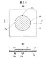
図14は、従来のマイクロストリップアンテナの一例の概略構成を示す図であり、同図(a)は正面図、同図(b)は同図(a)に示すD−D’切断線における断面図である。
【0003】
同図において、21は円形マイクロストリップ素子、22は誘電体基板、23は接地導体、24a,24bは励振導体、25a,25bは同軸接栓である。
【0004】
円形マイクロストリップ素子21は、図14に示すように、高周波特性の良好な誘電体基板22で保持させるか、あるいは、電界の最小となる円形の中心において保持具(スペーサ)により保持させることにより、接地導体23と適宜間隔を置いて平行に保たれる。
【0005】
この円形マイクロストリップ素子21の共振周波数(f)は、良く知られているように、下記(1)式で表される。
【0006】
【数1】
ここで、Dは円形マイクロストリップ素子21の直径、εrは誘電体基板22の比誘電率である。
【0008】
同軸接栓(25a,25b)の中心導体(芯線)と円形マイクロストリップ素子21とを、励振導体(25a,25b)を介して接続し、円形マイクロストリップ素子21に励振電力を給電することにより、この円形マイクロストリップ素子21はアンテナとして機能させることができる。
【0009】
この場合に、図14に示すように、同軸接栓(25a,25b)の中心導体、あるいは、励振導体(24a,24b)が、接地導体23に接触することがないように、同軸接栓(25a,25b)の中心導体部分の接地導体は部分的に取り除かれている。また、同軸接栓(25a,25b)の外部導体と接地導体23とは高周波的に接続されている。
【0010】
励振導体(24a,24b)と円形マイクロストリップ素子21との接続位置は同軸接栓(25a,25b)との整合を考慮して決定される。具体的には、円形マイクロストリップ素子21の中心に近づけるほど円形マイクロストリップ素子21の入力インピーダンスは低くなり、円形マイクロストリップ21の端部に近づけるほど円形マイクロストリップ素子21の入力インピーダンスは高くなる。これにより、円形マイクロストリップ素子21の入力インピーダンスを、任意に調整することが可能となる。
【0011】
また、図14に示すように、円形マイクロストリップ21の中心を通り直交した二直線上にそれぞれ励振導体24a、励振導体24bを設けることにより、モードが直交し、互いにほぼ独立することから、偏波共用を図ることが可能となる。
【0012】
このように、従来のマイクロストリップアンテナは、図14に示す円形または正方形の形状を採用することにより偏波共用が可能であるとともに、小型軽量で、薄型にできる等の利点を有している。
【0013】
【発明が解決しようとする課題】
図15は、図14に示すアンテナの指向性特性を示すグラフであり、同図(a)は磁界面内指向性、同図(b)は電界面内指向性を示している。
【0014】
なお、同図において、実線は同一偏波成分の指向性を示し、破線は交差偏波成分の指向性を示している。また、同図(a),(b)においては、円形マイクロストリップ素子21が作る面に対して直交方向の素子前面を基準の角度0°として計測し、その角度を横軸に、指向性減衰量(dB)を縦軸としている。
【0015】
図15から分かるように、放射最大方向における交差偏波成分は少ないものの、一旦角度が変化し始めると、交差偏波成分は増大してしまう。
【0016】
一方、偏波ダイバーシチアンテナが要求される移動通信用基地局アンテナ、あるいは、通信衛星(CS)からの直交する直線二偏波を受信する通信衛星用地球局アンテナとしては、広帯域の周波数特性が要求される。しかしながら、前記図14に示すマイクロストリップアンテナの周波数特性は、一般に狭帯域である。
【0017】
そのため、偏波ダイバーシチアンテナが要求される移動通信用基地局アンテナ、あるいは、通信衛星(CS)からの直交する直線二偏波を受信する通信衛星用地球局アンテナとして、マイクロストリップアンテナを使用する場合には、マイクロストリップアンテナの周波数特性を広帯域に変更する必要がある。
【0018】
このマイクロストリップアンテナの周波数特性を広帯域に変更するには、円形マイクロストリップ素子21と接地導体23との間隔を広めに設定すればよいが、この方法では、基本モード以外の高次モードも励振することになるため、交差偏波識別度を、さらに劣化させる要因となっていた。
【0019】
したがって、従来のマイクロストリップアンテナを、広角なサービスエリアでの偏波ダイバーシチブランチとして適用する場合には、指向性減衰量の増大による通信品質の劣化と相まって、ダイバーシチ利得の低下が懸念され、急激な通信品質の劣化につながる恐れがあった。
【0020】
なお、交差偏波識別度を向上させるには、円形マイクロストリップ素子21の中心を通る直線上で、中心に対して対称となる二点に「等振幅・逆相位相」の給電を行えばよいが、この方法では、給電回路が複雑な構成となるため、高価とならざるを得ず、また、薄型化を図ることが困難であるという問題点があった。
【0021】
本発明は、前記従来技術の問題点を解決するためになされたものであり、本発明の目的は、偏波共用アンテナにおいて、小型軽量、薄型化を図りながら、広角に渡って交差偏波成分を少なくすることが可能となる技術を提供することにある。
【0022】
本発明の他の目的は、偏波共用アンテナにおいて、小型軽量、薄型化を図りながら、広帯域の周波数特性を実現することが可能となる技術を提供することにある。
【0023】
本発明の前記目的並びにその他の目的及び新規な特徴は、本明細書の記載及び添付図面によって明らかにする。
【0024】
【課題を解決するための手段】
本願において開示される発明のうち、代表的なものの概要を簡単に説明すれば、下記の通りである。
【0026】
互いに対向する側の一端が第1の給電点対を構成し、ほぼ一直線状に設けられる第1および第2の線状導電体と、互いに対向する側の一端が第2の給電点対を構成し、前記第1の給電点対の間で前記第1の給電点対を結ぶ直線とほぼ直交する直線上に、前記第1の給電点対を結ぶ直線を挟んでほぼ一直線状に設けられる第3および第4の線状導電体と、前記各給電点対を取り囲むように設けられるn(n≧2)個のループ線状導電体と、i(i=2,・・n)番目のループ線状導電体と(i−1)番目のループ線状導電体との間に設けられる8×(i−1)個の短絡線状導電体と、前記各線状導電体、前記各ループ線状導電体および前記各短絡線状導電体と所定間隔を置いて設けられる接地導体とを具備する偏波共用アンテナであって、前記各線状導電体のそれぞれの他端を、前記n番目のループ線状導電体に接続するとともに、前記各線状導電体、前記各ループ線状導電体および前記各短絡線状導電体で分割される各領域の周囲長を、所定波長に設定する。
【0027】
前記偏波共用アンテナは、所定の厚みを有する誘電体基板を、さらに具備し、前記各線状導電体、前記各短絡線状導電体および前記各ループ線状導電体は、前記誘電体基板の表面に設けられ、前記接地導体は、前記誘電体基板の裏面に設けられる。
【0028】
前記偏波共用アンテナは、平衡−不平衡変換回路を、さらに具備し、前記第1の給電点対、あるいは、前記第2の給電点対の少なくも一方の給電点対に、前記平衡−不平衡変換回路を介して励振電力が給電される。
【0029】
前記偏波共用アンテナには、無給電素子が前置される。
【0030】
【発明の実施の形態】
以下、本発明の実施の形態を図面を参照して詳細に説明する。
【0031】
なお、発明の実施の形態を説明するための全図において、同一機能を有するものは同一符号を付け、その繰り返しの説明は省略する。
【0032】
[発明の実施の形態1]
図1は、本発明の一発明の実施の形態である偏波共用アンテナの概略構成を示す図であり、同図(a)は正面図、同図(b)は同図(a)のA−A’切断線における断面図である。
【0033】
同図において、1a,1b,1c,1dは、第1ないし第4の線状導電体、1eは、ループ状の線状導電体、2は誘電体基板、3は接地導体、4a,4b,4c,4dは励振導体、5a,5bは同軸接栓である。
【0034】
本実施の形態では、互いに直交する仮想直線上にある第1ないし第4の線状導電体(1a〜1d)と、この線状導電体(1a〜1d)の外側に設けられたループ状の線状導電体1eとで、メッシュ形素子1が構成される。
【0035】
ここで、第1の線状導電体(1a)と第2の線状導電体(1b)との互いに対向する側の一端は、第1の給電点対を構成し、同様に、第3の線状導電体(1c)と第4の線状導電体(1d)との互いに対向する側の一端は、第2の給電点対を構成する。また、ループ状の線状導電体(1e)には、前記各線状導電体(1a〜1d)のそれぞれの他端が接続される。
【0036】
このメッシュ形素子1は、図1に示すように、接地導体3と適宜間隔を置いて平行に保たれるように、高周波特性の良好な誘電体基板2で保持させるか、あるいは、波長に比べて極薄い誘電体基板上に配置させたメッシュ形素子1を、前記誘電体基板2から所定距離離れた適宜な位置に、保持具等を用いて支持するようにしてもよい。
【0037】
なお、各線状導電体(1a〜1e)は、例えば、銅線等の導線、あるいは、プリント配線手法または蒸着等により誘電体基板2の表面に設けられた銅箔等により構成される。
【0038】
本実施の形態のメッシュ形素子1は、同軸接栓(5a,5b)の中心導体および外部導体と、第1ないし第4の線状導電体(1a〜1d)のそれぞれ互いに対向する側の一端とを、励振導体(4a〜4d)を介して接続し、励振電力を給電することにより、アンテナとして機能させることができる。
【0039】
この場合に、接地導体3の背面に設けられた同軸接栓(5a,5b)の中心導体、あるいは、励振導体(4b,4d)が接地導体3と接触しないように、接地導体3における同軸接栓(5a,5b)の中心導体部分の接地導体は部分的に取り除かれている。また、同軸接栓(5a,5b)の外部導体と接地導体3とは高周波的に接続されている。
【0040】
具体的な給電としては、第1の線状導電体(1a)と第2の線状導電体(1b)との互いに対向する側の一端を、1つの偏波用の端子として用い、例えば、第2の線状導電体(1b)の一端に、同軸接栓(5a)の中心導体と接続される励振導体(4b)を接続した場合には、第1の線状導電体(1a)の一端に接続される励振導体(4a)を接地導体3に直接電気的に接続させることにより平衡給電に相似な形式とすることができる。
【0041】
また、同様に、前記した偏波とは直交する偏波を励振させるために、第4の線状導電体(1d)の一端に、同軸接栓(5b)の中心導体と接続される励振導体(4d)を接続した場合には、第3の線状導電体(1c)の一端に接続される励振導体(4a)を接地導体3に直接電気的に接続させることにより平衡給電に相似な形式とすることができる。
【0042】
なお、前記給電方法は一例を示したものであり、第1の線状導電体(1a)の一端と第2の線状導電体(1b)の一端、第3の線状導電体(1c)の一端と第4の線状導電体(1d)の一端とを入れ替えてもよく、また、各偏波間は独立しているため、使用しない偏波側の線状導電体(1aと1b、あるいは、1cと1d)は開放のままでもよいし、励振導体(4aと4b、あるいは、4cと4d)等を用いて接地導体3に接続するようにしてもよい。
【0043】
図2は、図1に示す偏波共用アンテナの指向性を示すグラフであり、同図(a)は磁界面内指向性を、同図(b)は電界面内指向性を示している。
【0044】
なお、図2においては、各線状導電体(1a〜1d)およびループ線状導電体(1e)として導線を使用し、図3(a)に示すように、メッシュ状素子1のループ状の線状導電体(1e)の一辺の長さ(S1)が0.318λo(λoは設計中心周波数における自由空間波長)、各線状導電体(1a〜1d)およびループ線状導電体(1e)の導体半径(ρ)が0.002λo、誘電体基板2の比誘電率(εr)がおおよそ1、誘電体基板2の厚さが0.0635λoであり、また、メッシュ状素子1に対して、第1の給電点対(第1の線状導電体(1a)と第2の線状導電体(1b)との互いに対向する側の一端)から平衡給電した場合の指向性を示している。
【0045】
さらに、図2(a),(b)においては、その角度(θ)は、図3(b)に示すように、メッシュ状素子1が作る面に対して直交方向(z)の素子前面を基準の角度0°として計測し、横軸に指向性減衰量(dB)を示している。さらに、磁界面内指向性は、図3(a)に示すy−z平面の指向性減衰量(dB)を、電界面内指向性は、図3(b)に示すをx−z平面の指向性減衰量(dB)を示している。
【0046】
図2から分かるように、指向性の半値幅は、磁界面において約75°、電界面で約60°となっている。いずれの場合においても、交差偏波の成分は−30dB以下に抑制されているため、図2には図示されていない。このように、本実施の形態の偏波共用アンテナでは、広角に渡り良好な交差偏波特性を得ることができる。
【0047】
図4は、図2と同じ条件下での、図1に示す偏波共用アンテナにおける50Ωに対するVSWR(定在波比)の周波数特性を示すグラフである。図4に示すように、本実施の形態の偏波共用アンテナは、従来のマイクロストリップアンテナにおいて、同じ誘電体基板2を用いて整合させた場合の特性と、ほぼ等価な特性を有している。
【0048】
しかしながら、本実施の形態の偏波共用アンテナでは、従来のマイクロストリップアンテナとは異なり、誘電体基板2の種類と厚さ、および、線状導電体(1a〜1e)の導体半径(ρ)を適宜調整することにより、アンテナの入力インピーダンスを変化させることが可能であるため、特別な整合回路を挿入することなく、アンテナの入力インピーダンスを整合させることが可能となる。
【0049】
また、本実施の形態の偏波共用アンテナにおいても、従来のマイクロストリップアンテナと同様、周波数帯域幅を拡大させるためには、誘電体基板2の比誘電率(εr)を下げ、その厚み(H)を増大させればよい。
【0050】
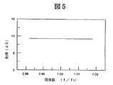
図5は、図2と同じ条件下での、図1に示す偏波共用アンテナにおける利得の周波数特性を示すグラフである。図5から分かるように、本実施の形態の偏波共用アンテナは、従来のマイクロストリップアンテナと同程度の特性を示す。
【0051】
なお、本実施の形態において、ループ状の線状導電体(1e)の形状は、図1に示す正方形に限定されるものではなく、例えば、図6に示すような円形であってもよい。
【0052】
また、メッシュ状素子1と短絡導体3とは、適当な保持具より空間的に所定距離間隔を置いて設けるようにしてもよい。
【0053】
[発明の実施の形態2]
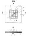
図7は、本発明の他の実施の形態である偏波共用アンテナの概略構成を示す図であり、同図(a)は正面図、同図(b)は同図(a)のB−B’切断線における断面図である。
【0054】
同図に示すように、本実施の形態の偏波共用アンテナは、前記実施の形態1の偏波共用アンテナのループ線状導電体(1e)のさらに外側に第2のループ線状導電体(1f)を設け、また、第1ないし第4の線状導電体(1a〜1d)のそれぞれの他端を延長して前記第2のループ線状導電体(1f)に接続するとともに、前記ループ線状導電体(1e)と第2のループ線状電導体(1f)との間を短絡する8個の短絡線状導電体(1g)を設けたものである。
【0055】
したがって、本実施の形態では、前記各線状導電体(1a〜1d)、前記各ループ線状導電体(1e,1f)および各短絡線状導電体(1g)により、前記ループ線状導電体(1f)に囲まれる領域が、4×4の小領域に分割される格子状(または碁盤の目状)のメッシュ状素子11が得られる。
【0056】
図8は、本実施の形態の偏波共用アンテナの指向性を表すグラフであり、同図(a)は磁界面内指向性を、同図(b)は電界面内指向性を示している。
【0057】
なお、図8においては、図9に示すように、格子状のメッシュ状素子11の核となる小さい閉じた正方形の周囲長が約1λo(図9に示すS2が0.25λ)、各線状導電体(1a〜1d)、各ループ線状導電体(1e,1f)および各短絡線状導電体(1g)の導体半径(ρ)が0.00316λo、誘電体基板2の比誘電率(εr)がおおよそ1、誘電体基板2の厚さが0.1λoである場合の指向性を示している。
【0058】
また、同図(a),(b)においては、その角度(θ)および指向性減衰量(dB)の定義は、図3(b)と同じである。
【0059】
図8から分かるように、本実施の形態の偏波共用アンテナでは、指向性の半値幅は、磁界面内において約40°、電界面内において約25°となっており、前記実施の形態の偏波共用アンテナと比べて、狭ビームとなっていることが分かる。
【0060】
いずれにしても、交差偏波の成分は−30dB以下に抑制されており、図8には図示されておらず、広角に渡り良好な交差偏波特性を得ることができる。
【0061】
図10は、図8に示す条件下での、図7に示す偏波共用アンテナにおける84Ωに対するVSWRの周波数特性を示すグラフである。図10のグラフから分かるように、本実施の形態の偏波共用アンテナでは、前記実施の形態の偏波共用アンテナより、帯域幅は若干狭くなっている。
【0062】
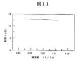
図11は、図8に示す条件下での、図7に示す偏波共用アンテナにおける利得の周波数特性を示すグラフである。図11のグラフから分かるように、本実施の形態の偏波共用アンテナは、前記実施の形態の偏波共用アンテナに比べて、利得が約3dB増大していることが分かる。
【0063】
従来のマイクロストリップアンテナにおいて、利得を増大させる場合には、複数のマイクロストリップ素子を適宜配列する必要があり、給電回路が複雑になるという欠点があるが、本実施の形態の偏波共用アンテナでは、格子状のメッシュ素子11を用いることにより、簡単な構成で、しかも物理的に見て薄型の形状を維持したまま、利得を増大させることが可能となる。
【0064】
[発明の実施の形態3]
図12は、本発明の他の実施の形態である偏波共用アンテナの概略構成を示す図であり、同図(a)は正面図、同図(b)は同図(a)のC−C’切断線における断面図である。
【0065】
本実施の形態の偏波共用アンテナは、前記実施の形態1の偏波共用アンテナに無給電素子6を前置したものである。この無給電素子6は、図12に示すように、第1の線状導電体(6a)、第2の線状導電体(6b)およびループ状の線状導電体(6c)とからなり、メッシュ状素子1と相似なメッシュ形状で構成されている。
【0066】
なお、この無給電素子6は、前記誘電体基板2から所定距離離れた適宜な位置に、保持具等を用いて支持される。
【0067】
本実施の形態においては、無給電素子6を用いることにより、複同調回路と等価となるので、周波数帯域幅を変化させることが可能であり、広帯域に渡ってVSWRを安定に保つことが可能である他、導波器や反射器として機能させることも可能なことから、指向特性を変化させることが可能となる。
【0068】
なお、無給電素子6は、必ずしも、メッシュ状素子1と相似なメッシュ形状である必要はなく、用途によっては、板状の導電体、あるいは、孔の空いた導電体で、大きさを調整したものであってもよい。
【0069】
図13は、前記各実施の形態における給電回路の他の例の概略構成を示す断面図である。
【0070】
図13に示す給電回路は、分岐導体による平衡−不平衡変換器を用いたものである。同図において、7は同軸線路、9は分岐導体、10は短絡板、7a、9aは中心導体(芯線)で、中心導体7aと中心導体9aとは、折曲部分8により一体化されている。なお、この分岐導体による平衡−不平衡変換器はよく知られている平衡−不平衡変換器路である。
【0071】
図13に示すような分岐導体による平衡−不平衡変換器を用いると、入力インピーダンスの調整範囲が広いため、整合が容易となり、また、周波数に対して依存することなく、平衡−不平衡変換を行うことができる。
【0072】
なお、平衡−不平衡変換器としては、図13に示す分岐導体による平衡−不平衡変換器の他に、例えば、同軸分割形、あるいは、コイルを用いたもの等、他の平衡−不平衡変換器を用いてもよいことは周知の通りである。
【0073】
以上、本発明を発明の実施の形態に基づき具体的に説明したが、本発明は、前記発明の実施の形態に限定されるものではなく、その要旨を逸脱しない範囲で種々変更し得ることは言うまでもない。
【0074】
【発明の効果】
本願において開示される発明のうち代表的なものによって得られる効果を簡単に説明すれば、下記の通りである。
【0075】
(1)本発明によれば、小型軽量、薄型化を図り、かつ、広角に渡って交差偏波成分の少ない偏波共用アンテナを得ることが可能となる。したがって、広角なサービスエリアでの偏波ダイバーシチブランチ等に用いることが可能である。
【0076】
(2)本発明によれば、特別な整合手段を挿入することなく、同軸給電線と入力インピーダンスを整合させることができるので、構成を単純化させることができ、コストを低減させることが可能となる。
【0077】
(3)本発明によれば、無給電素子を前置させることにより、VSWRの広帯域化と指向性の調整とが可能となるので、多様な無線ゾーンの設計に有用である。
【図面の簡単な説明】
【図1】本発明の一発明の実施の形態である偏波共用アンテナの概略構成を示す図である。
【図2】図1に示す偏波共用アンテナの指向性を示すグラフである。
【図3】図2に示す指向性の測定面を説明するための図である。
【図4】図2と同じ条件下での、図1に示す偏波共用アンテナにおける50Ωに対するVSWR(定在波比)の周波数特性を示すグラフである。
【図5】図2と同じ条件下での、図1に示す偏波共用アンテナにおける利得の周波数特性を示すグラフである。
【図6】本実施の形態1の偏波共用アンテナの変形例を示す図である。
【図7】本発明の他の実施の形態である偏波共用アンテナの概略構成を示す図である。
【図8】本実施の形態2の偏波共用アンテナの指向性を表すグラフである。
【図9】図8に示すグラフの測定方法を説明するための図である。
【図10】図8に示す条件下での、図7に示す偏波共用アンテナにおける84Ωに対するVSWRの周波数特性を示すグラフである。
【図11】図8に示す条件下での、図7に示す偏波共用アンテナにおける利得の周波数特性を示すグラフである。
【図12】本発明の他の実施の形態である偏波共用アンテナの概略構成を示す図である。
【図13】前記各実施の形態における給電回路の他の例の概略構成を示す断面図である。
【図14】従来のマイクロストリップアンテナの一例の概略構成を示す図である。
【図15】図14に示すアンテナの指向性特性を示すグラフである。
【符号の説明】
1,11…メッシュ状素子、1a,1b,1c,1d,1g,6a,6b…線状導電体、1e,1f,6c…ループ状の線状導電体、2,22…誘電体基板、3,23…接地導体、4a,4b,4c,4d,24a,24b…励振導体、5a,5b,25a,25b…同軸接栓,7…同軸線路、9…分岐線路、21…円形マイクロストリップ素子。[0001]
BACKGROUND OF THE INVENTION
The present invention relates to a dual-polarized antenna, and particularly, a mobile communication base station antenna that requires a polarization diversity antenna in a planar shape, or a communication that receives orthogonal two linearly polarized waves from a communication satellite (CS). The present invention relates to an effective technology applied to a satellite earth station antenna.
[0002]
[Prior art]
14A and 14B are diagrams showing a schematic configuration of an example of a conventional microstrip antenna. FIG. 14A is a front view, and FIG. 14B is a cross-sectional view taken along the line DD ′ shown in FIG. FIG.
[0003]
In the figure, 21 is a circular microstrip element, 22 is a dielectric substrate, 23 is a ground conductor, 24a and 24b are excitation conductors, and 25a and 25b are coaxial connectors.
[0004]
As shown in FIG. 14, the
[0005]
The resonance frequency (f) of the
[0006]
[Expression 1]
Here, D is the diameter of the
[0008]
By connecting the central conductor (core wire) of the coaxial connector (25a, 25b) and the
[0009]
In this case, as shown in FIG. 14, the coaxial connector (25a, 25b) is connected so that the center conductor or the excitation conductor (24a, 24b) does not contact the
[0010]
The connection position between the excitation conductors (24a, 24b) and the
[0011]
Further, as shown in FIG. 14, since the
[0012]
As described above, the conventional microstrip antenna has advantages such as being able to share polarization by adopting the circular or square shape shown in FIG. 14, and being small and light and thin.
[0013]
[Problems to be solved by the invention]
FIGS. 15A and 15B are graphs showing the directivity characteristics of the antenna shown in FIG. 14. FIG. 15A shows the in-plane directionality of the magnetic field, and FIG. 15B shows the in-plane directionality of the electric field.
[0014]
In the figure, the solid line indicates the directivity of the same polarization component, and the broken line indicates the directivity of the cross polarization component. In FIGS. 4A and 4B, the element front surface in the direction orthogonal to the surface formed by the
[0015]
As can be seen from FIG. 15, the cross polarization component in the maximum radiation direction is small, but once the angle starts to change, the cross polarization component increases.
[0016]
On the other hand, a base station antenna for mobile communication that requires a polarization diversity antenna or an earth station antenna for a communication satellite that receives two orthogonal linearly polarized waves from a communication satellite (CS) requires broadband frequency characteristics. Is done. However, the frequency characteristic of the microstrip antenna shown in FIG. 14 is generally a narrow band.
[0017]
Therefore, when a microstrip antenna is used as a base station antenna for mobile communication that requires a polarization diversity antenna or an earth station antenna for a communication satellite that receives orthogonal two linearly polarized waves from a communication satellite (CS). Therefore, it is necessary to change the frequency characteristic of the microstrip antenna to a wide band.
[0018]
In order to change the frequency characteristic of the microstrip antenna to a wide band, the distance between the
[0019]
Therefore, when a conventional microstrip antenna is applied as a polarization diversity branch in a wide-angle service area, there is a concern about a decrease in diversity gain, coupled with a deterioration in communication quality due to an increase in directional attenuation, which is abrupt. There was a risk of communication quality degradation.
[0020]
In order to improve the cross-polarization discrimination, “equal amplitude / antiphase phase” power supply may be performed on two points that are symmetrical with respect to the center on the straight line passing through the center of the
[0021]
The present invention has been made in order to solve the above-described problems of the prior art, and an object of the present invention is to achieve cross polarization components over a wide angle while reducing the size, weight and thickness of a polarization sharing antenna. It is an object of the present invention to provide a technique that can reduce the amount of the noise.
[0022]
Another object of the present invention is to provide a technique capable of realizing a broadband frequency characteristic while reducing the size, weight and thickness of a dual-polarized antenna.
[0023]
The above and other objects and novel features of the present invention will become apparent from the description of the present specification and the accompanying drawings.
[0024]
[Means for Solving the Problems]
Of the inventions disclosed in this application, the outline of typical ones will be briefly described as follows.
[0026]
One end on the opposite side constitutes a first feeding point pair, the first and second linear conductors provided in a substantially straight line, and one end on the opposite side constitutes a second feeding point pair The first feed point pair is provided on a straight line that is substantially orthogonal to a straight line that connects the first feed point pair, and is provided in a substantially straight line with a straight line that connects the first feed point pair interposed therebetween. 3 and 4 linear conductors, n (n ≧ 2) loop linear conductors provided so as to surround each of the feeding point pairs, and i (i = 2,... N) th loop 8 × (i−1) short-circuited linear conductors provided between the linear conductor and the (i−1) -th loop linear conductor, the linear conductors, and the loop linear elements A polarization sharing antenna comprising a conductor and each of the short-circuited linear conductors and a ground conductor provided at a predetermined interval, The other ends of the linear conductors are connected to the n-th loop linear conductor, and are divided by the linear conductors, the loop linear conductors, and the short-circuit linear conductors. The perimeter of each region is set to a predetermined wavelength.
[0027]
The dual-polarized antenna further includes a dielectric substrate having a predetermined thickness, and each linear conductor, each short-circuit linear conductor, and each loop linear conductor is a surface of the dielectric substrate. The ground conductor is provided on the back surface of the dielectric substrate.
[0028]
The dual-polarized antenna further includes a balanced-unbalanced conversion circuit, and the balanced-unbalanced circuit is connected to at least one of the first feeding point pair or the second feeding point pair. Excitation power is supplied through the balance conversion circuit.
[0029]
A parasitic element is placed in front of the polarization sharing antenna.
[0030]
DETAILED DESCRIPTION OF THE INVENTION
Hereinafter, embodiments of the present invention will be described in detail with reference to the drawings.
[0031]
Note that components having the same function are denoted by the same reference symbols throughout the drawings for describing the embodiment of the invention, and the repetitive description thereof is omitted.
[0032]
FIG. 1 is a diagram showing a schematic configuration of a dual-polarized antenna according to an embodiment of the present invention. FIG. 1 (a) is a front view, and FIG. 1 (b) is A in FIG. It is sectional drawing in a -A 'cutting line.
[0033]
In the figure, 1a, 1b, 1c, and 1d are first to fourth linear conductors, 1e is a loop-like linear conductor, 2 is a dielectric substrate, 3 is a ground conductor, 4a, 4b, 4c and 4d are excitation conductors, and 5a and 5b are coaxial plugs.
[0034]
In the present embodiment, the first to fourth linear conductors (1a to 1d) on virtual lines orthogonal to each other, and the loop-like shape provided outside the linear conductors (1a to 1d) The mesh-shaped
[0035]
Here, one end of the first linear conductor (1a) and the second linear conductor (1b) facing each other constitutes a first feeding point pair, and similarly, One end of the linear conductor (1c) and the fourth linear conductor (1d) facing each other constitutes a second feeding point pair. The other end of each of the linear conductors (1a to 1d) is connected to the loop-shaped linear conductor (1e).
[0036]
As shown in FIG. 1, the
[0037]
In addition, each linear conductor (1a-1e) is comprised by the copper foil etc. which were provided on the surface of the
[0038]
The
[0039]
In this case, the coaxial conductor in the
[0040]
As specific power feeding, one end of the first linear conductor (1a) and the second linear conductor (1b) facing each other is used as one polarization terminal, for example, When the excitation conductor (4b) connected to the central conductor of the coaxial plug (5a) is connected to one end of the second linear conductor (1b), the first linear conductor (1a) By directly electrically connecting the excitation conductor (4a) connected to one end to the
[0041]
Similarly, an excitation conductor connected to the center conductor of the coaxial plug (5b) at one end of the fourth linear conductor (1d) in order to excite a polarization orthogonal to the above-described polarization. When (4d) is connected, the excitation conductor (4a) connected to one end of the third linear conductor (1c) is directly electrically connected to the
[0042]
In addition, the said electric power feeding method shows an example, and the end of 1st linear conductor (1a), the end of 2nd linear conductor (1b), and 3rd linear conductor (1c) And one end of the fourth linear conductor (1d) may be interchanged, and since each polarization is independent, the polarization-side linear conductors (1a and 1b, or 1c and 1d) may be left open, or may be connected to the
[0043]
2 is a graph showing the directivity of the dual-polarized antenna shown in FIG. 1. FIG. 2A shows the directivity in the magnetic field plane, and FIG. 2B shows the directivity in the electric field plane.
[0044]
In FIG. 2, conductive wires are used as the respective linear conductors (1a to 1d) and the loop linear conductor (1e), and as shown in FIG. The length (S1) of one side of the linear conductor (1e) is 0.318λo (λo is a free space wavelength at the design center frequency), the conductors of the linear conductors (1a to 1d) and the loop linear conductor (1e) The radius (ρ) is 0.002λo, the relative permittivity (εr) of the
[0045]
Further, in FIGS. 2 (a) and 2 (b), as shown in FIG. 3 (b), the angle (θ) is set so that the element front surface in the direction (z) orthogonal to the plane formed by the mesh-
[0046]
As can be seen from FIG. 2, the full width at half maximum of directivity is about 75 ° on the magnetic field surface and about 60 ° on the electric field surface. In either case, the cross-polarized wave component is suppressed to −30 dB or less and is not shown in FIG. As described above, in the dual-polarized antenna according to the present embodiment, it is possible to obtain good cross polarization characteristics over a wide angle.
[0047]
FIG. 4 is a graph showing frequency characteristics of VSWR (standing wave ratio) with respect to 50Ω in the dual-polarized antenna shown in FIG. 1 under the same conditions as FIG. As shown in FIG. 4, the dual-polarized antenna according to the present embodiment has characteristics that are substantially equivalent to the characteristics of a conventional microstrip antenna that is matched using the same
[0048]
However, in the dual-polarized antenna according to the present embodiment, unlike the conventional microstrip antenna, the type and thickness of the
[0049]
Also, in the dual-polarized antenna according to the present embodiment, in order to increase the frequency bandwidth, the relative permittivity (εr) of the
[0050]
FIG. 5 is a graph showing frequency characteristics of gain in the dual-polarized antenna shown in FIG. 1 under the same conditions as in FIG. As can be seen from FIG. 5, the dual-polarized antenna according to the present embodiment exhibits the same characteristics as the conventional microstrip antenna.
[0051]
In the present embodiment, the shape of the loop-shaped linear conductor (1e) is not limited to the square shown in FIG. 1, and may be, for example, a circle as shown in FIG.
[0052]
Further, the mesh-
[0053]
[
FIG. 7 is a diagram showing a schematic configuration of a dual-polarized antenna according to another embodiment of the present invention. FIG. 7 (a) is a front view, and FIG. It is sectional drawing in a B 'cutting line.
[0054]
As shown in the figure, the dual-polarized antenna according to the present embodiment has a second loop linear conductor (1e) further outside the loop linear conductor (1e) of the dual-polarized antenna according to the first embodiment. 1f), the other ends of the first to fourth linear conductors (1a to 1d) are extended and connected to the second loop linear conductor (1f), and the loop Eight short-circuited linear conductors (1g) for short-circuiting between the linear conductor (1e) and the second loop linear conductor (1f) are provided.
[0055]
Therefore, in the present embodiment, each of the linear conductors (1a to 1d), each of the loop linear conductors (1e, 1f), and each of the short-circuited linear conductors (1g), the loop linear conductor ( A mesh-
[0056]
FIG. 8 is a graph showing the directivity of the dual-polarized antenna according to this embodiment. FIG. 8A shows the directivity in the magnetic field plane, and FIG. 8B shows the directivity in the electric field plane. .
[0057]
In FIG. 8, as shown in FIG. 9, the circumference of a small closed square that is the core of the lattice-
[0058]
Further, in FIGS. 3A and 3B, the definition of the angle (θ) and the directivity attenuation (dB) is the same as that in FIG. 3B.
[0059]
As can be seen from FIG. 8, in the dual-polarized antenna of this embodiment, the directivity half-width is about 40 ° in the magnetic field plane and about 25 ° in the electric field plane. It can be seen that the beam is narrower than the dual-polarized antenna.
[0060]
In any case, the cross polarization component is suppressed to −30 dB or less, and is not shown in FIG. 8, and a good cross polarization characteristic can be obtained over a wide angle.
[0061]
FIG. 10 is a graph showing the frequency characteristics of VSWR with respect to 84Ω in the dual-polarized antenna shown in FIG. 7 under the conditions shown in FIG. As can be seen from the graph of FIG. 10, the bandwidth of the dual-polarized antenna of this embodiment is slightly narrower than that of the dual-polarized antenna of the above-described embodiment.
[0062]
FIG. 11 is a graph showing the frequency characteristics of gain in the dual-polarized antenna shown in FIG. 7 under the conditions shown in FIG. As can be seen from the graph of FIG. 11, it can be seen that the dual-polarized antenna of the present embodiment has an increase of about 3 dB in comparison with the dual-polarized antenna of the above-described embodiment.
[0063]
In the case of increasing the gain in the conventional microstrip antenna, it is necessary to arrange a plurality of microstrip elements as appropriate, and there is a disadvantage that the feeding circuit becomes complicated. However, in the polarization sharing antenna of this embodiment, By using the grid-
[0064]
FIG. 12 is a diagram showing a schematic configuration of a dual-polarized antenna according to another embodiment of the present invention, in which FIG. 12 (a) is a front view and FIG. It is sectional drawing in a C 'cutting line.
[0065]
The dual-polarized antenna according to the present embodiment is obtained by placing a
[0066]
The
[0067]
In the present embodiment, by using the
[0068]
The
[0069]
FIG. 13 is a cross-sectional view showing a schematic configuration of another example of the power feeding circuit in each of the embodiments.
[0070]
The power feeding circuit shown in FIG. 13 uses a balanced-unbalanced converter with a branch conductor. In the figure, 7 is a coaxial line, 9 is a branch conductor, 10 is a short circuit plate, 7a and 9a are center conductors (core wires), and the center conductor 7a and the
[0071]
When a balanced-unbalanced converter using branch conductors as shown in FIG. 13 is used, the adjustment range of the input impedance is wide, so that matching is easy, and balanced-unbalanced conversion can be performed without depending on the frequency. It can be carried out.
[0072]
As the balanced-unbalanced converter, in addition to the balanced-unbalanced converter using the branch conductor shown in FIG. 13, other balanced-unbalanced conversion such as a coaxial split type or a coil is used. As is well known, a vessel may be used.
[0073]
The present invention has been specifically described above based on the embodiments of the invention. However, the present invention is not limited to the embodiments of the invention, and various modifications can be made without departing from the scope of the invention. Needless to say.
[0074]
【The invention's effect】
The effects obtained by the representative ones of the inventions disclosed in the present application will be briefly described as follows.
[0075]
(1) According to the present invention, it is possible to obtain a dual-polarized antenna that is small, light, and thin, and has few cross polarization components over a wide angle. Therefore, it can be used for a polarization diversity branch or the like in a wide-angle service area.
[0076]
(2) According to the present invention, the coaxial feeder and the input impedance can be matched without inserting special matching means, so that the configuration can be simplified and the cost can be reduced. Become.
[0077]
(3) According to the present invention, it is possible to widen the bandwidth of the VSWR and adjust the directivity by placing the parasitic element in front, which is useful for designing various wireless zones.
[Brief description of the drawings]
FIG. 1 is a diagram showing a schematic configuration of a dual-polarized antenna according to an embodiment of the present invention.
2 is a graph showing the directivity of the dual-polarized antenna shown in FIG.
FIG. 3 is a diagram for explaining a directivity measurement surface shown in FIG. 2;
4 is a graph showing frequency characteristics of VSWR (standing wave ratio) with respect to 50Ω in the dual-polarized antenna shown in FIG. 1 under the same conditions as in FIG. 2;
5 is a graph showing frequency characteristics of gain in the dual-polarized antenna shown in FIG. 1 under the same conditions as those in FIG.
6 is a diagram showing a modification of the dual-polarized antenna according to
FIG. 7 is a diagram showing a schematic configuration of a dual-polarized antenna according to another embodiment of the present invention.
FIG. 8 is a graph showing the directivity of the dual-polarized antenna according to the second embodiment.
9 is a diagram for explaining a method of measuring the graph shown in FIG.
10 is a graph showing frequency characteristics of VSWR with respect to 84Ω in the dual-polarized antenna shown in FIG. 7 under the conditions shown in FIG.
11 is a graph showing frequency characteristics of gain in the dual-polarized antenna shown in FIG. 7 under the conditions shown in FIG.
FIG. 12 is a diagram showing a schematic configuration of a dual-polarized antenna according to another embodiment of the present invention.
FIG. 13 is a cross-sectional view illustrating a schematic configuration of another example of the power feeding circuit in each of the embodiments.
FIG. 14 is a diagram showing a schematic configuration of an example of a conventional microstrip antenna.
15 is a graph showing the directivity characteristics of the antenna shown in FIG.
[Explanation of symbols]
DESCRIPTION OF
Claims (4)
Translated fromJapanese互いに対向する側の一端が第2の給電点対を構成し、前記第1の給電点対の間で前記第1の給電点対を結ぶ直線とほぼ直交する直線上に、前記第1の給電点対を結ぶ直線を挟んでほぼ一直線状に設けられる第3および第4の線状導電体と、
前記各給電点対を取り囲むように設けられるn(n≧2)個のループ線状導電体と、
i(i=2,・・n)番目のループ線状導電体と(i−1)番目のループ線状導電体との間に設けられる8×(i−1)個の短絡線状導電体と、
前記各線状導電体、前記各ループ線状導電体および前記各短絡線状導電体と所定間隔を置いて設けられる接地導体とを具備する偏波共用アンテナであって、
前記各線状導電体のそれぞれの他端を、前記n番目のループ線状導電体に接続するとともに、前記各線状導電体、前記各ループ線状導電体および前記各短絡線状導電体で分割される各領域の周囲長を、所定波長に設定したことを特徴とする偏波共用アンテナ。The first and second linear conductors that are arranged in a substantially straight line, with one end on the opposite side constituting the first feeding point pair,
One end on the opposite side forms a second feeding point pair, and the first feeding point is on a straight line that is substantially orthogonal to a straight line connecting the first feeding point pair between the first feeding point pair. Third and fourth linear conductors provided in a substantially straight line across a straight line connecting the point pairs;
N (n ≧ 2) loop linear conductors provided so as to surround each of the feeding point pairs;
8 × (i−1) short-circuited linear conductors provided between the i (i = 2,... n) th loop linear conductor and the (i−1) th loop linear conductor. When,
Each of the linear conductors, each of the loop linear conductors, and each of the short-circuited linear conductors and a grounded conductor provided at a predetermined interval,
The other end of each linear conductor is connected to the nth loop linear conductor and is divided by each linear conductor, each loop linear conductor, and each short-circuit linear conductor. A dual-polarized antenna, wherein the perimeter of each region is set to a predetermined wavelength.
Priority Applications (1)
| Application Number | Priority Date | Filing Date | Title |
|---|---|---|---|
| JP05069297AJP3804878B2 (en) | 1997-03-05 | 1997-03-05 | Dual-polarized antenna |
Applications Claiming Priority (1)
| Application Number | Priority Date | Filing Date | Title |
|---|---|---|---|
| JP05069297AJP3804878B2 (en) | 1997-03-05 | 1997-03-05 | Dual-polarized antenna |
Publications (2)
| Publication Number | Publication Date |
|---|---|
| JPH10247818A JPH10247818A (en) | 1998-09-14 |
| JP3804878B2true JP3804878B2 (en) | 2006-08-02 |
Family
ID=12865986
Family Applications (1)
| Application Number | Title | Priority Date | Filing Date |
|---|---|---|---|
| JP05069297AExpired - Fee RelatedJP3804878B2 (en) | 1997-03-05 | 1997-03-05 | Dual-polarized antenna |
Country Status (1)
| Country | Link |
|---|---|
| JP (1) | JP3804878B2 (en) |
Families Citing this family (9)
| Publication number | Priority date | Publication date | Assignee | Title |
|---|---|---|---|---|
| US7057558B2 (en)* | 2002-06-27 | 2006-06-06 | Matsushita Electric Industrial Co., Ltd. | Antenna device |
| JP2004104678A (en)* | 2002-09-12 | 2004-04-02 | Matsushita Electric Ind Co Ltd | Antenna device |
| JP2004128932A (en)* | 2002-10-03 | 2004-04-22 | Matsushita Electric Ind Co Ltd | Antenna device |
| JP2007150675A (en)* | 2005-11-28 | 2007-06-14 | Toppan Forms Co Ltd | Non-contact communication body |
| US8878737B2 (en) | 2009-06-29 | 2014-11-04 | Blackberry Limited | Single feed planar dual-polarization multi-loop element antenna |
| JP5050084B2 (en)* | 2010-08-26 | 2012-10-17 | 日本電業工作株式会社 | antenna |
| CN103855461B (en)* | 2012-12-06 | 2016-05-11 | 瑞声声学科技(深圳)有限公司 | Antenna |
| JP5974057B2 (en)* | 2014-09-08 | 2016-08-23 | 電気興業株式会社 | Thin antenna |
| JP6971350B2 (en)* | 2020-03-17 | 2021-11-24 | ソフトバンク株式会社 | Antenna device, wireless communication device and mobile body |
- 1997
- 1997-03-05JPJP05069297Apatent/JP3804878B2/ennot_activeExpired - Fee Related
Also Published As
| Publication number | Publication date |
|---|---|
| JPH10247818A (en) | 1998-09-14 |
Similar Documents
| Publication | Publication Date | Title |
|---|---|---|
| JP3085524B2 (en) | Dipole antenna with reflector | |
| US6759990B2 (en) | Compact antenna with circular polarization | |
| JP5745582B2 (en) | Antenna and sector antenna | |
| US11955738B2 (en) | Antenna | |
| JP3734666B2 (en) | ANTENNA DEVICE AND ARRAY ANTENNA USING THE SAME | |
| US6600455B2 (en) | M-shaped antenna apparatus provided with at least two M-shaped antenna elements | |
| KR20060066717A (en) | Wideband Multi-Dipole Antenna with Frequency-Independent Radiation Characteristics | |
| US10971820B2 (en) | Arrangement comprising antenna elements | |
| JP2020509691A (en) | Bowtie antenna device | |
| US9263807B2 (en) | Waveguide or slot radiator for wide E-plane radiation pattern beamwidth with additional structures for dual polarized operation and beamwidth control | |
| US7151505B2 (en) | Quadrifilar helix antenna | |
| CN111585015B (en) | Microstrip line coupling feed broadband circularly polarized eight-arm slot spiral antenna | |
| JP4073130B2 (en) | Cross dipole antenna | |
| JP3804878B2 (en) | Dual-polarized antenna | |
| JPH07303005A (en) | Antenna system for vehicle | |
| JP4516246B2 (en) | antenna | |
| JP2000278039A (en) | Dual-polarized antenna | |
| JP2000031732A (en) | Dual-polarized antenna | |
| JP4503459B2 (en) | Multi-frequency antenna | |
| CN118369820A (en) | Antenna device having two stacked radiating elements | |
| JP4108246B2 (en) | Loop antenna | |
| JP2011199350A (en) | Antenna | |
| JP2545663B2 (en) | Tilt beam antenna | |
| JP2006014152A (en) | Planar antenna | |
| JP3364204B2 (en) | Antenna device |
Legal Events
| Date | Code | Title | Description |
|---|---|---|---|
| A621 | Written request for application examination | Free format text:JAPANESE INTERMEDIATE CODE: A621 Effective date:20040210 | |
| A977 | Report on retrieval | Free format text:JAPANESE INTERMEDIATE CODE: A971007 Effective date:20050909 | |
| A131 | Notification of reasons for refusal | Free format text:JAPANESE INTERMEDIATE CODE: A131 Effective date:20050920 | |
| A521 | Written amendment | Free format text:JAPANESE INTERMEDIATE CODE: A523 Effective date:20051117 | |
| TRDD | Decision of grant or rejection written | ||
| A01 | Written decision to grant a patent or to grant a registration (utility model) | Free format text:JAPANESE INTERMEDIATE CODE: A01 Effective date:20060502 | |
| A61 | First payment of annual fees (during grant procedure) | Free format text:JAPANESE INTERMEDIATE CODE: A61 Effective date:20060508 | |
| R150 | Certificate of patent or registration of utility model | Free format text:JAPANESE INTERMEDIATE CODE: R150 | |
| FPAY | Renewal fee payment (event date is renewal date of database) | Free format text:PAYMENT UNTIL: 20090519 Year of fee payment:3 | |
| FPAY | Renewal fee payment (event date is renewal date of database) | Free format text:PAYMENT UNTIL: 20120519 Year of fee payment:6 | |
| FPAY | Renewal fee payment (event date is renewal date of database) | Free format text:PAYMENT UNTIL: 20130519 Year of fee payment:7 | |
| R250 | Receipt of annual fees | Free format text:JAPANESE INTERMEDIATE CODE: R250 | |
| R250 | Receipt of annual fees | Free format text:JAPANESE INTERMEDIATE CODE: R250 | |
| LAPS | Cancellation because of no payment of annual fees |