JP3801464B2 - Hybrid connector - Google Patents
Hybrid connectorDownload PDFInfo
- Publication number
- JP3801464B2 JP3801464B2JP2001185972AJP2001185972AJP3801464B2JP 3801464 B2JP3801464 B2JP 3801464B2JP 2001185972 AJP2001185972 AJP 2001185972AJP 2001185972 AJP2001185972 AJP 2001185972AJP 3801464 B2JP3801464 B2JP 3801464B2
- Authority
- JP
- Japan
- Prior art keywords
- optical element
- connector
- sleeve
- optical
- element module
- Prior art date
- Legal status (The legal status is an assumption and is not a legal conclusion. Google has not performed a legal analysis and makes no representation as to the accuracy of the status listed.)
- Expired - Fee Related
Links
- 230000003287optical effectEffects0.000claimsdescription269
- 230000013011matingEffects0.000claimsdescription12
- 238000000034methodMethods0.000description46
- 238000003780insertionMethods0.000description14
- 230000037431insertionEffects0.000description13
- 239000013307optical fiberSubstances0.000description13
- 229920003002synthetic resinPolymers0.000description8
- 239000000057synthetic resinSubstances0.000description8
- 239000000463materialSubstances0.000description7
- 230000005540biological transmissionEffects0.000description4
- 239000002184metalSubstances0.000description4
- 239000000758substrateSubstances0.000description4
- 229920000049Carbon (fiber)Polymers0.000description3
- 239000004917carbon fiberSubstances0.000description3
- VNWKTOKETHGBQD-UHFFFAOYSA-NmethaneChemical compoundCVNWKTOKETHGBQD-UHFFFAOYSA-N0.000description3
- 230000001105regulatory effectEffects0.000description3
- 239000000470constituentSubstances0.000description2
- 238000010586diagramMethods0.000description2
- 238000005192partitionMethods0.000description2
- 230000007175bidirectional communicationEffects0.000description1
- 230000001276controlling effectEffects0.000description1
- 230000000694effectsEffects0.000description1
- 239000003822epoxy resinSubstances0.000description1
- 239000000835fiberSubstances0.000description1
- 239000011521glassSubstances0.000description1
- 235000013372meatNutrition0.000description1
- 239000004033plasticSubstances0.000description1
- 229920000647polyepoxidePolymers0.000description1
- 230000001902propagating effectEffects0.000description1
- 229920005989resinPolymers0.000description1
- 239000011347resinSubstances0.000description1
Images


Classifications
- G—PHYSICS
- G02—OPTICS
- G02B—OPTICAL ELEMENTS, SYSTEMS OR APPARATUS
- G02B6/00—Light guides; Structural details of arrangements comprising light guides and other optical elements, e.g. couplings
- G02B6/24—Coupling light guides
- G02B6/42—Coupling light guides with opto-electronic elements
- G02B6/4201—Packages, e.g. shape, construction, internal or external details
- G02B6/4274—Electrical aspects
- G02B6/4277—Protection against electromagnetic interference [EMI], e.g. shielding means
- G—PHYSICS
- G02—OPTICS
- G02B—OPTICAL ELEMENTS, SYSTEMS OR APPARATUS
- G02B6/00—Light guides; Structural details of arrangements comprising light guides and other optical elements, e.g. couplings
- G02B6/24—Coupling light guides
- G02B6/36—Mechanical coupling means
- G02B6/38—Mechanical coupling means having fibre to fibre mating means
- G02B6/3807—Dismountable connectors, i.e. comprising plugs
- G02B6/381—Dismountable connectors, i.e. comprising plugs of the ferrule type, e.g. fibre ends embedded in ferrules, connecting a pair of fibres
- G02B6/3817—Dismountable connectors, i.e. comprising plugs of the ferrule type, e.g. fibre ends embedded in ferrules, connecting a pair of fibres containing optical and electrical conductors
- G—PHYSICS
- G02—OPTICS
- G02B—OPTICAL ELEMENTS, SYSTEMS OR APPARATUS
- G02B6/00—Light guides; Structural details of arrangements comprising light guides and other optical elements, e.g. couplings
- G02B6/24—Coupling light guides
- G02B6/36—Mechanical coupling means
- G02B6/38—Mechanical coupling means having fibre to fibre mating means
- G02B6/3807—Dismountable connectors, i.e. comprising plugs
- G02B6/3897—Connectors fixed to housings, casing, frames or circuit boards
- G—PHYSICS
- G02—OPTICS
- G02B—OPTICAL ELEMENTS, SYSTEMS OR APPARATUS
- G02B6/00—Light guides; Structural details of arrangements comprising light guides and other optical elements, e.g. couplings
- G02B6/24—Coupling light guides
- G02B6/42—Coupling light guides with opto-electronic elements
- G02B6/4201—Packages, e.g. shape, construction, internal or external details
- G02B6/4204—Packages, e.g. shape, construction, internal or external details the coupling comprising intermediate optical elements, e.g. lenses, holograms
- G02B6/421—Packages, e.g. shape, construction, internal or external details the coupling comprising intermediate optical elements, e.g. lenses, holograms the intermediate optical component consisting of a short length of fibre, e.g. fibre stub
- G—PHYSICS
- G02—OPTICS
- G02B—OPTICAL ELEMENTS, SYSTEMS OR APPARATUS
- G02B6/00—Light guides; Structural details of arrangements comprising light guides and other optical elements, e.g. couplings
- G02B6/24—Coupling light guides
- G02B6/42—Coupling light guides with opto-electronic elements
- G02B6/4201—Packages, e.g. shape, construction, internal or external details
- G02B6/4246—Bidirectionally operating package structures
- G—PHYSICS
- G02—OPTICS
- G02B—OPTICAL ELEMENTS, SYSTEMS OR APPARATUS
- G02B6/00—Light guides; Structural details of arrangements comprising light guides and other optical elements, e.g. couplings
- G02B6/24—Coupling light guides
- G02B6/42—Coupling light guides with opto-electronic elements
- G02B6/4292—Coupling light guides with opto-electronic elements the light guide being disconnectable from the opto-electronic element, e.g. mutually self aligning arrangements
- G02B6/4293—Coupling light guides with opto-electronic elements the light guide being disconnectable from the opto-electronic element, e.g. mutually self aligning arrangements hybrid electrical and optical connections for transmitting electrical and optical signals
- G—PHYSICS
- G02—OPTICS
- G02B—OPTICAL ELEMENTS, SYSTEMS OR APPARATUS
- G02B6/00—Light guides; Structural details of arrangements comprising light guides and other optical elements, e.g. couplings
- G02B6/24—Coupling light guides
- G02B6/42—Coupling light guides with opto-electronic elements
- G02B6/4201—Packages, e.g. shape, construction, internal or external details
- G02B6/4219—Mechanical fixtures for holding or positioning the elements relative to each other in the couplings; Alignment methods for the elements, e.g. measuring or observing methods especially used therefor
- G02B6/4228—Passive alignment, i.e. without a detection of the degree of coupling or the position of the elements
- G02B6/423—Passive alignment, i.e. without a detection of the degree of coupling or the position of the elements using guiding surfaces for the alignment
- G—PHYSICS
- G02—OPTICS
- G02B—OPTICAL ELEMENTS, SYSTEMS OR APPARATUS
- G02B6/00—Light guides; Structural details of arrangements comprising light guides and other optical elements, e.g. couplings
- G02B6/24—Coupling light guides
- G02B6/42—Coupling light guides with opto-electronic elements
- G02B6/4292—Coupling light guides with opto-electronic elements the light guide being disconnectable from the opto-electronic element, e.g. mutually self aligning arrangements
Landscapes
- Physics & Mathematics (AREA)
- General Physics & Mathematics (AREA)
- Optics & Photonics (AREA)
- Electromagnetism (AREA)
- Optical Couplings Of Light Guides (AREA)
- Optical Communication System (AREA)
- Mechanical Coupling Of Light Guides (AREA)
- Manufacturing Of Electrical Connectors (AREA)
- Connector Housings Or Holding Contact Members (AREA)
- Led Device Packages (AREA)
- Light Receiving Elements (AREA)
Description
Translated fromJapanese【0001 】
【発明の属する技術分野】
本発明は、一度の接続作業で電気コネクタ及び光コネクタの接続が完了するように、電気コネクタと光コネクタを一体に構成したハイブリッドコネクタの組み付け方法及びハイブリッドコネクタに関する。
【0002 】
【従来の技術】
自動車をはじめとする様々な車両においては、各種センサよりの信号、及び各種エレクトロニクス機器を制御するための制御信号が非常に多く、これらの信号を個別の信号線を使用して伝送しようとする場合には、その信号線の本数が膨大となり、ワイヤハーネスが非常に重たくなってしまっていた。また、近年、各種エレクトロニクス機器からの伝送情報が大容量化、高密度化してきていることから、ワイヤハーネスが一層重たくなってしまっている。このようなことから、近年ではワイヤハーネスの一部を光ファイバケーブル(光ファイバコード)に置き換え、例えば各ノード間を光ファイバケーブルで接続するようなシステムを採用するようになってきた。
【0003 】
ところで、ワイヤハーネスの一部を光ファイバケーブルに置き換えようとすると、例えばカーメーカーにおいては電気コネクタや光コネクタの接続作業が煩雑になってしまうことになる。そこで最近では、電気コネクタ及び光コネクタの接続作業が一度で完了してしまうような、電気コネクタと光コネクタを一体に備えたハイブリッドコネクタの実用化が進められている。
【0004 】
【発明が解決しようとする課題】
しかしながらハイブリッドコネクタは、電気コネクタと光コネクタとを一体にした構成であることから、部品点数が多くなり、特に光コネクタに係る部分の組み付けが面倒であって、作業工数がかなり掛かってしまうという問題点があった。また、光コネクタを構成する光素子モジュールの位置が組み付けの際に安定しないといった問題点もあった。
【0005 】
組み付けの際に光素子モジュールの位置が不安定であると、作業性に影響を来してしまうことになり、場合によっては、組み付け後においての光の損失にも影響を来してしまう恐れがある。
【0006 】
そこで本発明は、組み付け作業を簡素化するとともに、光素子モジュールの位置を安定させて作業性の向上と光の損失の低減とを図ることができるハイブリッドコネクタの組み付け方法及びハイブリッドコネクタを提供することを課題とする。
【0007】
【課題を解決するための手段】
上記課題を解決するためなされた請求項1記載の本発明のハイブリッドコネクタは、電気コネクタと光コネクタとを一体に備え,光コネクタは、光素子を有する少なくとも一つの光素子モジュールと、光導波路を有し光素子モジュールの数に応じて設けられるスリーブと、電気コネクタと共用になるとともにスリーブを保持する受承筒を相手側コネクタと嵌合する側と反対側に突出して形成したハウジングと、光素子モジュールを保持するとともに光素子モジュールのハウジングに対しての位置決めをするケースとを有し,受承筒のスリーブが挿し込まれる側には、受承筒の軸方向に凹む凹部を形成し、光素子モジュールには、凹部に係合し光素子の位置を軸に合わせる凸部を形成することを特徴としている。
【0008】
上記課題を解決するためなされた請求項2記載の本発明のハイブリッドコネクタは、電気コネクタと光コネクタとを一体に備え,光コネクタは、光素子を有する少なくとも一つの光素子モジュールと、光導波路を有し前記光素子モジュールの数に応じて設けられるスリーブと、電気コネクタと共用になるとともにスリーブを保持する受承筒を相手側コネクタと嵌合する側と反対側に突出して形成したハウジングと、光素子モジュールを保持するとともに光素子モジュールのハウジングに対しての位置決めをするケースとを有し,受承筒のスリーブが挿し込まれる側には、光素子モジュールを載せてケース取り付け前の光素子モジュールの回動を規制する壁を形成することを特徴としている。
【0009】
請求項3記載の本発明のハイブリッドコネクタは、請求項2に記載のハイブリッドコネクタにおいて,受承筒に、壁に対向するとともにこの壁とで光素子モジュールを挟み込む第二の壁を形成することを特徴としている。
【0010】
上記課題を解決するためなされた請求項4記載の本発明のハイブリッドコネクタは、電気コネクタと光コネクタとを一体に備え、光コネクタは、光素子を有する少なくとも一つの光素子モジュールと、光導波路を有し光素子モジュールの数に応じて設けられるスリーブと、電気コネクタと共用になるとともにスリーブを保持する受承筒を相手側コネクタと嵌合する側と反対側に突出して形成したハウジングと、ハウジングに挿着され受承筒と共にスリーブを保持するスリーブホルダーと、光素子モジュールを保持するとともに光素子モジュールのハウジングに対しての位置決めをするケースとを有し,受承筒のスリーブが挿し込まれる側及び/又はスリーブホルダーの端部には、受承筒の軸方向に凹む凹部を形成し、光素子モジュールには、凹部に係合し光素子の位置を軸に合わせる凸部を形成することを特徴としている。
【0011】
上記課題を解決するためなされた請求項5記載の本発明のハイブリッドコネクタは、電気コネクタと光コネクタとを一体に備え,光コネクタは、光素子を有する少なくとも一つの光素子モジュールと、光導波路を有し光素子モジュールの数に応じて設けられるスリーブと、電気コネクタと共用になるとともにスリーブを保持する受承筒を相手側コネクタと嵌合する側と反対側に突出して形成したハウジングと、ハウジングに挿着され受承筒と共にスリーブを保持するスリーブホルダーと、光素子モジュールを保持するとともに光素子モジュールのハウジングに対しての位置決めをするケースとを有し,受承筒の前記スリーブが挿し込まれる側及び/又はスリーブホルダーの端部には、光素子モジュールを載せてケース取り付け前の光素子モジュールの回動を規制する壁を形成することを特徴としている。
【0012】
請求項6記載の本発明のハイブリッドコネクタは、請求項5に記載のハイブリッドコネクタにおいて,受承筒及び/又はスリーブホルダーに、壁に対向するとともに壁とで光素子モジュールを挟み込む第二の壁を形成することを特徴としている。
【0031】
請求項1に記載された本発明によれば、ハイブリッドコネクタは、光素子モジュールの凸部がハウジング側の凹部に係合する構造になっている。これにより、光素子の位置が受承筒の軸に合わせられる。また、これらが係合した後には、ガタ付き難くなり、その後の組み付けにおいて光素子モジュールの位置が安定する。従って、作業性が向上する。また、光の損失を低減することができるようになる。
【0032】
請求項2に記載された本発明によれば、ハイブリッドコネクタは、光素子モジュールを載せてその回動を規制する壁を有する構造になっている。これにより、光素子モジュールの回動による位置ズレが規制される。その後の組み付けにおいて光素子モジュールの位置が安定する。従って、作業性が向上する。また、光の損失を低減することができるようになる。
【0034】
請求項3に記載された本発明によれば、ハイブリッドコネクタは、光素子モジュールの回動を規制する一対の壁を有する構造になっている。光素子モジュールは、その一対の壁に挟まれ回動が規制される。光素子モジュールが挟まれることにより、確実に回動が規制される。従って、その後の組み付けにおいて光素子モジュールの位置が安定し、作業性が一層向上する。また、より一層、光の損失の低減を図ることができるようになる。
【0035】
請求項4に記載された本発明によれば、ハイブリッドコネクタは、光素子モジュールの凸部がハウジング側及び/又はスリーブホルダーの凹部に係合する構造になっている。これにより、光素子の位置が受承筒の軸に合わせられる。また、これらが係合した後には、ガタ付き難くなり、その後の組み付けにおいて光素子モジュールの位置が安定する。従って、作業性が向上する。また、光の損失を低減することができるようになる。
【0036】
請求項5に記載された本発明によれば、ハイブリッドコネクタは、光素子モジュールを載せてその回動を規制する壁を有する構造になっている。これにより、光素子モジュールの回動による位置ズレが規制される。その後の組み付けにおいて光素子モジュールの位置が安定する。従って、作業性が向上する。また、光の損失を低減することができるようになる。
【0038】
請求項6に記載された本発明によれば、ハイブリッドコネクタは、光素子モジュールの回動を規制する一対の壁を有する構造になっている。光素子モジュールは、その一対の壁に挟まれ回動が規制される。光素子モジュールが挟まれることにより、確実に回動が規制される。従って、その後の組み付けにおいて光素子モジュールの位置が安定し、作業性が一層向上する。また、より一層、光の損失の低減を図ることができるようになる。
【0039 】
【発明の実施の形態】
以下、図面を参照して本発明の一実施の形態を説明する。
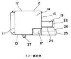
図1は本発明の一実施の形態を示すハイブリッドコネクタの分解斜視図である。また、図2はハイブリッドコネクタの正面図、図3はハイブリッドコネクタの平面図、図4はハイブリッドコネクタの左側面図、図5はハウジングの右側面図を示している。
【0040 】
尚、本明細書中において、ハイブリッドコネクタとは電気コネクタと光コネクタとを一体にした構成のコネクタであるものとする。
【0041 】
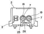
図1において、引用符号1は図示しないプリント基板上に実装される雄形のハイブリッドコネクタを示している。そのハイブリッドコネクタ1は、互いにハウジング2を共用する電気コネクタ3と光コネクタ4とで構成されている。本発明のハイブリッドコネクタ1は、後述するが、そのハイブリッドコネクタ1に係る組み付け作業が簡単に行えるように構成されている。また、後述する光素子モジュール8、9の位置が組み付けにおいて安定するように構成されている。
【0042 】
ハイブリッドコネクタ1には、雌形のハイブリッドコネクタ5が接続されるようになっている。その接続相手の雌形のハイブリッドコネクタ5には、端末にフェルールを装着した光ファイバケーブル(光ファイバコード)が二本、ハウジング内部に並んで取り付けられている(不図示)。二本の光ファイバケーブルのうちの一本は送信用であり、もう一本は受信用である。上記フェルールの先端面には光ファイバケーブルの心線部分(コア及びクラッドからなる(プラスチック)光ファイバ)が露出しており、後述するスリーブ7、7の光導波路28、28と光軸が合うようになっている。
【0043 】
上記電気コネクタ3は、ハウジング2と電気端子(PCB端子)6とを備えて構成されている。また、上記光コネクタ4は、ハウジング2とスリーブ7、7と光素子モジュール8、9とシールドケース10とを備えて構成されている。尚、光コネクタ4の光素子モジュール8、9は、受・発光モジュール、受・送信モジュール、FOT(Fiber Optic Transceiver )等で呼ばれることもある。また、シールドケース10は特許請求の範囲に記載したケースに相当するものである。
【0044 】
以下、ハイブリッドコネクタ1の上記各構成部材について説明する(図1ないし図5いずれかを参照するものとする)。各構成部材についての説明の後には、ハイブリッドコネクタ1の組み付け(組み付け方法)について詳細に説明するものとする。
【0045 】
上記ハウジング2は、絶縁性を有する合成樹脂材により前面11が解放された矩形箱状に形成されている。すなわち、ハウジング2は上壁12、下壁13、右側壁14、左側壁15、奥壁16を備えて矩形箱状に形成されている。上壁12には、ロック部が形成されており、ハイブリッドコネクタ5に設けられたロッキングアームが嵌合するようになっている。また、右側壁14及び左側壁15には、ポケット状の固定ピン収容部17、17が形成されており、金属製の固定ピン18、18がそこに収容され係合するようになっている。固定ピン収容部17、17には、上記プリント基板側に開口する孔が貫通形成されており、固定ピン18、18の一部がその孔を介して上記プリント基板に固定されるようになっている。
【0046 】
ハウジング2の奥壁16には、一対の受承筒19、19が一体に形成されている。受承筒19、19は、内側の断面形状が円形となる筒状に形成されている。また、スリーブ7、7に応じた長さを有している。さらに、受承筒19、19は、上壁12、下壁13、右側壁14、左側壁15、及び奥壁16で囲まれるハイブリッドコネクタ5に対しての嵌合部20内に突出するとともに、奥壁16の後方にも突出するように形成されている。尚、嵌合部20側からは、上記フェルールが挿し込まれるようになっている。
【0047 】
受承筒19、19の中間であってその内面には、例えば各三つの突起21(図6参照。以下同様)が形成されている。各三つの突起21は、受承筒19、19の長手方向に沿って形成されており、また、120°のピッチで形成されている。三つの突起21の先端で描く円弧の直径は、スリーブ7の直径よりも若干小さくなるように形成されており、受承筒19、19に挿し込まれたスリーブ7、7が三つの突起21を押し潰しながら圧入されるようになっている。尚、三つの突起21に接触するまでは、スリーブ7、7がスムーズに挿し込めるように内径が設定されているものとする。
【0048 】
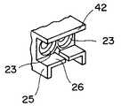
受承筒19、19の外側であってスリーブ7、7が挿し込まれる側の端部には、略環状に突出する係合部22、22が一体に形成されている。また、上記端部の端面には、受承筒19、19の軸に沿って凹む凹部23、23(図6又は図15参照)が形成されている。さらに、受承筒19、19の外側であって右側壁14及び左側壁15側の側面には、段部24、24が形成されている。さらにまた、下壁13側には、脚部25が連成されている。
【0049 】
係合部22、22は、その突出方向が受承筒19、19の軸に直交する方向に一致して形成されており、厚みは前記軸の方向に沿った力に対して抗することができるだけの剛性を有するように形成されている。係合部22、22には、シールドケース10が係合するようになっている。
【0050 】
凹部23、23は、受承筒19、19の内径よりも大きな径で形成されており、光素子モジュール8、9の後述する凸部35、35が係合するようになっている。段部24、24は、前記軸に沿って形成されており、シールドケース10の後述する抜け止め部41、41が係合するようになっている。
【0051 】
脚部25は、断面視略コ字状(肉盗み部分を含めると断面視略H字状)に形成されており、受承筒19、19の上記端部の端面よりも後方に突出する部分には、その端面に直交する壁26が形成されている。壁26は、光素子モジュール8、9に対する回り止めであり、本形態においては平坦な面を有するように形成されている。
【0052 】
尚、ハウジング2の下壁13には、上記プリント基板に挿し込まれる突起27、27が一体に形成されている。
【0053 】
上記電気端子6は、導電性を有する既知のL字状の雄端子であって、そのL字状に折り曲げられた一方の部分側が奥壁16を介してハウジング2の嵌合部20内に位置し、且つ、他方の部分側が上記プリント基板に固定されるようになっている。本形態の電気端子6は、ハウジング2に対し上下二段(各段二つ)に装着されることから、長さの異なる二種類の端子を備える必要がある。
【0054 】
上記スリーブ7、7は、コア及びクラッドからなる光導波路28、28と円筒状のホルダー29、29とで構成されている。尚、光導波路28、28は、上記光ファイバケーブルの心線部分と同等の屈折率を有することが好ましい。また、スリーブ7、7を上記光ファイバケーブルで形成することも可能である(所定長さに切断して端面を例えば研磨すればよい)。
【0055 】
上記光素子モジュール8は、複数のリードフレーム30とモールド部(不図示)とケース31とを備えて構成されている。複数のリードフレーム30のうちの一つには、発光素子(不図示)がマウントされている。また、ワイヤボンディングがなされている。複数のリードフレーム30の下側は、上記プリント基板に固定(半田付け)されるようになっている。発光素子(不図示)は、光素子モジュール8の中心(又は上記モールド部の中心)よりも光素子モジュール9側に位置するように設けられている(上記中心にあってもよいが光素子モジュール9側にズレている方がハイブリッドコネクタ1をコンパクトにすることができる)。発光素子は特許請求の範囲に記載した光素子に相当するものであって、例えば発光ダイオード(LED)を挙げることができる。
【0056 】
モールド部は、光の伝搬が可能な透明樹脂材(例えばエポキシ樹脂、上記光ファイバケーブルの心線部分と同等の屈折率を有することが好ましい)で成形されている。また、複数のリードフレーム30の略上半分を埋設するようになっている。モールド部によって発光素子等が外部から保護されるようになっている。
【0057 】
上記光素子モジュール9は、複数のリードフレーム32とモールド部(不図示上述のモールド部と同じであり説明を省略する)とケース33とを備えて構成されている。複数のリードフレーム31のうちの一つには、受光素子(不図示)がマウントされている。また、ワイヤボンディングがなされている。複数のリードフレーム31の下側は、上記プリント基板に固定(半田付け)されるようになっている。受光素子(不図示)は、光素子モジュール9の中心(又は上記モールド部の中心)よりも光素子モジュール8側に位置するように設けられている(上記中心にあってもよいが光素子モジュール8側にズレている方がハイブリッドコネクタ1をコンパクトにすることができる)。受光素子は特許請求の範囲に記載した光素子に相当するものであって、例えばフォトダイオード(PD)を挙げることができる。
【0058 】
尚、本形態において、発光素子(不図示)と受光素子(不図示)とが互いに近接する方向にズレていることから、ハイブリッドコネクタ1がコンパクトに構成されている。また、光素子モジュール8の一部が電気端子6に対し間隔を存して重なるように配置されていることから、一層、ハイブリッドコネクタ1がコンパクトに構成されている。
【0059 】
ケース31及びケース33は、カーボンファイバ等を含有した導電性を有する合成樹脂材(絶縁性を有する合成樹脂材でもよい)から成り、上記モールド部を覆うケース本体34、34と、ケース本体34、34から突出する筒状の凸部35、35とで構成されている。
【0060 】
ケース本体34、34は、有底の箱状に形成されており、上記モールド部が若干の圧入状態で挿入されるようになっている。ケース本体34、34の開口縁部(上記モールド部を挿入するための開口縁部)は平坦に形成されており、その開口縁部が組み付けの際に上記壁26に載せられるようになっている。尚、上記開口縁部の反対側に位置する壁も平坦に形成されている。
【0061 】
凸部35、35は、発光素子(不図示)及び受光素子(不図示)の位置に対応して形成されている。また、凸部35、35は、円筒状であることから、発光素子(不図示)、受光素子(不図示)を臨むことができるようになっている。凸部35、35は、組み付けの際、上記凹部23、23に係合するようになっている。
【0062 】
上記シールドケース10は、導電性を有する金属薄板をプレス加工して形成されるとともに、組み付け等に有用なバネ性が持たせられている。また、シールドケース10は、隔壁36によって隔てられる二つの収容部37、37を有している。その収容部37、37には、U字状の切り欠き部38、38と、光素子モジュール8、9を切り欠き部38、38側に押し付ける凸部39、39(図12参照 一つのみ図示)と、脚状の基板固定部40、40とが形成されている。
【0063 】
収容部37、37は、光素子モジュール8、9を収容するようになっており、組み付けの際に上記係合部22、22と共に光素子モジュール8、9が収容されると、その光素子モジュール8、9が上記バネ性によって圧入状態で保持されるようになる。
【0064 】
尚、光素子モジュール8、9を受承筒19、19の端面に押し付けるようなバネ性を有することができれば、シールドケース10をカーボンファイバ等を含有した導電性を有する合成樹脂材で形成することができる。シールドケース10に導電性をもたせることで、光素子モジュール8、9に対するシールド性を高めることができる。
【0065 】
切り欠き部38、38は、受承筒19、19の外径に合わせて切り欠き形成されており、その縁部には内方へ突出する突起状の抜け止め部41、41が形成されている。抜け止め部41、41は、シールドケース10を受承筒19、19に組み付けると、その受承筒19、19の段部24、24に係合するようになっている。すなわち、抜け止め部41、41は、シールドケース10の抜けを規制することができるようになっている。
【0066 】
凸部39、39(図12参照 一つのみ図示)は、切り欠き部38、38を形成した前壁の反対側となる後壁に形成されている。また、切り欠き部38、38より臨む位置に打ち出しによって例えば楕円状に突出形成されている。基板固定部40、40は、収容部37、37の側壁に連成されており、上記プリント基板に固定されるようになっている。また、基板固定部40、40は、グランド端子の役割を果たすようになっている。
【0067 】
次に、ハイブリッドコネクタ1の組み付け(組み付け方法)についてその一例を詳細に説明する。尚、予め電気端子6がハウジング2に装着されるものとする。ここでは、それ以降となる光コネクタ4に係る部分の組み付け(組み付け方法)について説明する。
【0068 】
電気コネクタ3に係る部分が組み付けられた後、光コネクタ4に係る部分は、第一組み付け工程、第二組み付け工程、第三組み付け工程を順に経て組み付けられる。
【0069 】
尚、上記第二組み付け工程とは、特許請求の範囲に記載した第二″組み付け工程に相当する工程であるものとする(特許請求の範囲に記載した第二組み付け工程は、以下の説明の中で壁26の内容を除いたものである。また、特許請求の範囲に記載した第二′組み付け工程は、以下の説明の中で凸部35、35及び凹部23、23の内容を除いたものである)。
【0070 】
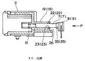
先ず、第一組み付け工程について図6、図7の断面図と図8の背面図を参照しながら説明する。図6はスリーブ挿し込み前の断面図、図7はスリーブ挿し込み途中の仮挿入状態の断面図、図8は図7の状態での背面図である。
【0071 】
図6において、スリーブ7、7の側面を持ちながら、そのスリーブ7、7を矢線P方向に移動させる。スリーブ7、7は、受承筒19、19の上記端面に向けて移動する。そして、スリーブ7、7を受承筒19、19の上記端面より挿し込みさらに矢線P方向に移動させると、図7に示される如く、スリーブ7、7の端部に突起21が接触する。この時、スリーブ7、7は、その途中まで受承筒19、19に挿し込まれた状態になる(仮挿入状態)。図8に示される如く、スリーブ7、7が二本とも仮挿入状態になると、次の第二組み付け工程(特許請求の範囲に記載した第二″組み付け工程に相当)に移行する。
【0072 】
第二組み付け工程は図9、図10の断面図と図11の背面図を参照しながら説明する。図9は光素子モジュールを押し付け始めた状態の断面図、図10は光素子モジュールを押し付けた後の本挿入状態の断面図、図11は図10の状態での背面図である。
【0073 】
図9において、第二組み付け工程に移行すると、光素子モジュール8、9を受承筒19、19から露出したスリーブ7、7の端面にセットする。スリーブ7、7の端面は、凸部35、35に収容され、その状態で光素子モジュール8、9を矢線P方向に押し付けると、スリーブ7、7は突起21を押し潰しながらさらに挿し込まれ、図10に示される如くの状態になる(本挿入状態)。光素子モジュール8、9の凸部35、35は、受承筒19、19の凹部23、23に挿し込まれて係合し、上記発光素子、上記受光素子の位置が受承筒19、19の軸(スリーブ7、7の軸)に合わせられる。また、光素子モジュール8、9は、壁26によってその回動が規制された状態(図10及び図11参照)になる。固定ピン18、18の組み付けも例えばここで行われる。
【0074 】
この時、スリーブ7、7の挿し込み量が光素子モジュール8、9によって決定される。また、スリーブ7、7及び光素子モジュール8、9の間に間隙はなく、光の間隙損失が最小限に抑えられる状態になる。さらに、光素子モジュール8、9の凸部35、35が受承筒19、19の凹部23、23に挿し込まれ、各軸が合うことで軸ズレによる光の損失が低減されるような状態になる(軸を合わせるのは上記の位置でなくても良いものとする)。
【0075 】
第二組み付け工程では、スリーブ7、7の端面を光素子モジュール8、9で押し付けていることから、その端面が手の脂等で汚れてしまうことはなく、組み付けによる伝送効率の低下が防止される。
【0076 】
尚、図14及び図15に示される如く、壁26の反対側に第二の壁42を対向配置させれば、光素子モジュール8、9が挟み込まれた状態になり回動規制が一層確実になる。これにより、第三組み付け工程でのシールドケース10の組み付けが容易になる。
【0077 】
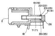
上記本挿入状態になると、次の第三組み付け工程に移行する。第三組み付け工程は図12、図13の断面図を参照しながら説明する。図12はシールドケース取り付け前の断面図、図13は組み付けが完了した状態の断面図である。
【0078 】
図12において、第三組み付け工程に移行すると、矢線Q方向からシールドケース10を組み付ける。シールドケース10は、図13に示される如く、光素子モジュール8、9を保持しつつ、係合部22、22に係合する。光素子モジュール8、9は、シールドケース10により押し付けられ、受承筒19、19の上記端面に密着する。光素子モジュール8、9は、その位置が固定される。
【0079 】
尚、光素子モジュール8、9の回動が規制されていることから、シールドケース10の組み付けが簡単に行われる。
【0080 】
以上説明したように、ハイブリッドコネクタ1は、第一組み付け工程、第二組み付け工程(特許請求の範囲に記載した第二″組み付け工程に相当 以下同様)、及び第三組み付け工程を含んで組み付けられる。すなわち、ハイブリッドコネクタ1の光コネクタ4に係る部分が上記第一〜第三組み付け工程により組み付けられる。
【0081 】
上記第一〜第三組み付け工程をまとめてみると、第一組み付け工程では、スリーブ7、7の仮挿入が行われ、受承筒19、19の途中までスリーブ7、7が挿し込まれる。第二組み付け工程では、光素子モジュール8、9の押し付けによってスリーブ7、7がさらに受承筒19、19内に挿し込まれる。スリーブ7、7は受承筒19、19に対し本挿入状態になる。この時、凸部35、35が凹部23、23に係合し、光素子の位置が受承筒19、19の軸に合わせられる。また、光素子モジュール8、9はハウジング2の壁26に載せられ又はハウジング2の一対の壁(壁26、第二の壁42)に挟まれる。
【0082 】
第二組み付け工程では、スリーブ7、7の組み付けと光素子モジュール8、9の組み付けとが同時に行われる。スリーブ7、7と光素子モジュール8、9は、個々に組み付けられるものではないから、作業が簡素化されることになる。
【0083 】
また、第二組み付け工程では、光素子モジュール8、9の凸部35、35がハウジング2側の凹部23、23に係合するから、ガタ付き難く、その後の光素子モジュール8、9の位置が安定する。また、光素子モジュール8、9がハウジング2の壁26に載せられ又はハウジング2の一対の壁(壁26、第二の壁42)に挟まれるから、光素子モジュール8、9の回動による位置ズレが規制され、その後の光素子モジュール8、9の位置が安定する。これにより、作業性の向上と光の損失の低減を図ることができるようになる。
【0084 】
第三組み付け工程では、シールドケース10を用いて光素子モジュール8、9を保持させる。シールドケース10は受承筒19、19に係合し、その結果、光素子モジュール8、9の位置が固定される。ここでも個々に組み付けられるものではないから、作業が簡素化されることになる。尚、第二組み付け工程でのスリーブ7、7の移動量を、第一組み付け工程での移動量よりも小さくすれば、圧入に係る労力が低減される。
【0085 】
一方、ハイブリッドコネクタ1は、上述のような構成であることから、光素子の位置を受承筒19、19の軸に合わせることができる。また、光素子モジュール8、9の回動による位置ズレを規制することができる。従って、光素子モジュール8、9の位置を安定させ、光の損失の低減と作業性の向上とを図ることができる。
【0086 】
続いて、本発明の他の一実施の形態を説明する。
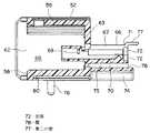
図16は本発明の他の一実施の形態を示すハイブリッドコネクタの分解斜視図、図17はハウジングの断面図である。
【0087 】
図16において、引用符号51は図示しないプリント基板上に実装される雄形のハイブリッドコネクタを示している。そのハイブリッドコネクタ51は、互いにハウジング52を共用する電気コネクタ53と光コネクタ54とを有して構成されており、上述のハイブリッドコネクタ1(図1参照)と同様に組み付けに係る作業が簡単に行えるようになっている。また、上述の光素子モジュール8、9の位置が組み付けにおいて安定するように構成されている。
【0088 】
ハイブリッドコネクタ51には、雌形のハイブリッドコネクタ5(図1参照)が接続されるようになっている。そのハイブリッドコネクタ5(図1参照)の図示しないフェルールの先端面には、後述するレンズスリーブ56、56が光学的に結合するようになっている(光軸が一致する)。
【0089 】
上記電気コネクタ53は、ハウジング52と上述の電気端子(PCB端子)6とを備えて構成されている。また、上記光コネクタ54は、ハウジング52と、スリーブホルダー55と、レンズスリーブ56、56(特許請求の範囲に記載したスリーブに相当)と、光素子モジュール8、9と、シールドケース57(特許請求の範囲に記載したケースに相当)とを備えて構成されている。
【0090 】
以下、ハイブリッドコネクタ51の上記各構成部材について説明する(図16又は図17を参照するものとする)。また、各構成部材についての説明の後には、ハイブリッドコネクタ51の組み付け(組み付け方法)について詳細に説明する。
【0091 】
上記ハウジング52は、絶縁性を有する合成樹脂材により前面58が解放された矩形箱状に形成されている。すなわち、ハウジング52は上壁59、下壁60、右側壁61、左側壁62、奥壁63を備えて矩形箱状に形成されている。上壁59には、ロック部が形成されており、ハイブリッドコネクタ5(図1参照)に設けられたロッキングアームが嵌合するようになっている。また、右側壁61及び左側壁62には、ポケット状の固定ピン収容部64、64(一方のみ図示)が形成されており、金属製の固定ピン65、65がそこに収容され係合するようになっている。固定ピン収容部64、64には、上記プリント基板側に開口する孔が貫通形成されており、固定ピン65、65の一部がその孔を介して上記プリント基板に固定されるようになっている。
【0092 】
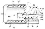
ハウジング52の奥壁63には、一対の受承筒66、66が一体に形成されている。その受承筒66、66は、上側に切り欠き部67を有しており、スリーブホルダー55をハウジング52に挿着(本形態においては受承筒66、66に挿着)してその切り欠き部67を塞ぐと、内側の断面形状が円形となる筒状に形成されている。また、受承筒66、66は、レンズスリーブ56、56に応じた長さを有して形成されている。さらに、受承筒66、66は、上壁59、下壁60、右側壁61、左側壁62、及び奥壁63で囲まれたハイブリッドコネクタ5(図1参照)に対しての嵌合部68内と、奥壁63の後方とに突出するように形成されている。尚、受承筒66、66の間には、スリーブホルダー55の後述する垂直壁80を案内するスリット(不図示)が切り欠き形成されている。また、受承筒66、66は、嵌合部68側から上記フェルールがそれぞれ挿し込まれるようになっている。
【0093 】
受承筒66、66の内面には、レンズスリーブ56、56に対するストッパ69、69(一方のみ図示)と光軸合わせ用の突起70、70(一方のみ図示)とがそれぞれ形成されている。そのストッパ69、69は、嵌合部68側に形成されており、レンズスリーブ56、56の後述するフランジ部88、88が当接するようになっている。これに対し、突起70、70は、奥壁63の後方側に形成されており、レンズスリーブ56、56の後述する光導波路86、86を支持するようになっている。すなわち、突起70、70は、断面視三角形状に形成されており、その頂部に上記光導波路86、86を載せて支持するようになっている(光軸合わせのために上記頂部はつぶれ可能に形成されている)。
【0094 】
受承筒66、66の外側であってレンズスリーブ56、56が挿し込まれる側の端部には、係合部71、71が一体に突出形成されている。また、上記端部の端面には、受承筒66、66の軸に沿って凹む凹部72、72が形成されている。さらに、受承筒66、66の外側であって右側壁61及び左側壁62側の側面には、段部73、73(一方のみ図示)が形成されている。さらにまた、下壁60側には、脚部74が連成されている。
【0095 】
係合部71、71には、シールドケース57が係合するようになっており、前記軸の方向に沿った力に対して抗することができるだけの剛性を有するように厚みが設定されて形成されている。尚、係合部71、71は、上述の係合部22、22(図1参照)を参考にして形成してもよいものとする。
【0096 】
凹部72、72は、受承筒66、66の内径よりも大きな径で形成されており、光素子モジュール8、9の凸部35、35が係合するようになっている。段部73、73は、シールドケース57の後述する抜け止め部94、94が係合するようになっている。
【0097 】
脚部74は、断面視略コ字状(肉盗みを兼ねたガイド部75を含めると断面視略H字状になる。上記ガイド部にはスリーブホルダー55の後述する水平壁81が進退自在になる)に形成されており、受承筒66、66の上記端部の端面よりも後方に突出する部分には、上述の壁26(図15参照)と同様の壁76が形成されている。その壁76は、光素子モジュール8、9に対する回り止めであり、平坦な面を有するように形成されている。本形態においては、壁76に対向する第二の壁77、77が係合部71、71に形成されている(壁76、77によって光素子モジュール8、9が挟み込まれ回り止めがなされるようになっている)。
【0098 】
ハウジング52の下壁60には、上記プリント基板に挿し込まれる突起78、78(一方のみ図示)が一体に形成されている。
【0099 】
上記スリーブホルダー55は、合成樹脂製であってハウジング52に挿着されると、受承筒66、66と共にレンズスリーブ56、56を保持することができるように形成されている。すなわち、スリーブホルダー55は、受承筒66、66の切り欠き部67を塞いでレンズスリーブ56、56を保持する保持部79、79と、その保持部79、79の間に垂設される垂直壁80と、垂直壁80の端部に連成される水平壁81とを有して構成されている。
【0100 】
保持部79、79には、その前端にレンズスリーブ56、56の後述するフランジ部88、88に当接する押圧部82、82が形成されている。また、保持部79、79の内面には、受承筒66、66の突起70、70に合わせた光軸合わせ用の突起83、83(一方のみ図示。突起70と同じ機能を有する)が形成されている。さらに、保持部79、79の後端には、受承筒66、66の凹部72、72に連続する凹部84、84(図20参照。一方のみ図示)と、第二の壁77、77の機能を有する壁85、85(特許請求の範囲に記載した第二の壁に相当)とが形成されている。
【0101 】
垂直壁80は、上述の如く受承筒66、66の上記スリットに案内される部分として形成されている。また、水平壁81は、上記ガイド部75に案内される部分として形成されている。
【0102 】
上記レンズスリーブ56、56は、透明な合成樹脂やガラスで形成されている。また、レンズスリーブ56、56は、側部がテーパとなる截頭円錐状の光導波路86、86と、その光導波路86、86の大径側の端面に形成される凸レンズ部87、87と、凸レンズ部87、87の外側に突出形成されるフランジ部88、88とを有して構成されている。さらに、レンズスリーブ56、56は、凸レンズ部87、87が上記フェルールの先端面に対向し、光導波路86、86の小径側の端面が光素子モジュール8、9の発光素子(不図示)、受光素子(不図示)に対向するように形成されている。
【0103 】
光導波路86、86の上記側部の上には、空気層が形成されるようになっており、光導波路86、86内を進行する光がその側部の境界で全反射するようになっている。フランジ部88、88の凸レンズ部87、87側の面は、受承筒66、66のストッパ69、69に当接するようになっている。また、フランジ部88、88の光導波路86、86側の面には、スリーブホルダー55の押圧部82、82が当接するようになっている。言い換えれば、押圧部82、82によって押圧され、ストッパ69、69に当接すると位置決めがなされるようになっている。
【0104 】
尚、以上のような凸レンズ部87、87を付けたスリーブに限定されるものではないものとする。フランジ部88、88を有していればよく、レンズスリーブ56、56の形状に対して凸レンズ部87、87がないものや、光導波路86、86がストレートに形成されたスリーブであってもよいものとする。
【0105 】
上記シールドケース57は、導電性を有する金属薄板をプレス加工して形成されている。また、シールドケース57は、組み付け等に有用なバネ性を持たせて形成されている。さらに、シールドケース57は、隔壁89によって隔てられた二つの収容部90、90を有するように構成されている。
【0106 】
収容部90、90は、光素子モジュール8、9を収容することができるように形成されており、組み付けの際に上記係合部71、71と共に光素子モジュール8、9を収容すると、その光素子モジュール8、9が上記バネ性によって圧入状態で保持されるようになっている。また、収容部90、90は、U字状の切り欠き部91、91と、光素子モジュール8、9を切り欠き部91、91側に押し付ける凸部92、92(図23参照。一つのみ図示)と、脚状の基板固定部93(三本のみ図示。本形態では四本あるものとする)とを有して構成されている。
【0107 】
尚、光素子モジュール8、9を受承筒66、66の端面に押し付けるバネ性を有することができるのであれば、シールドケース57を、カーボンファイバ等を含有させた導電性を有する合成樹脂材で形成することができるものとする。シールドケース57に導電性をもたせることで、光素子モジュール8、9に対するシールド性を高めることができるという利点がある。
【0108 】
切り欠き部91、91は、受承筒66、66の外径に合わせて切り欠き形成されており、その縁部の近傍にはバネ片状の抜け止め部94、94が形成されている。抜け止め部94、94は、シールドケース57を受承筒66、66に組み付けると、一端撓んだ後にその受承筒66、66の段部73、73の下部に先端が係合するようになっている。すなわち、抜け止め部94、94は、シールドケース57の抜けを規制することができるようになっている。
【0109 】
凸部92、92(図23参照。一つのみ図示)は、切り欠き部91、91を形成した前壁の反対側となる後壁に形成されている。また、切り欠き部91、91より臨む位置に打ち出しによって例えば楕円状に突出形成されている。基板固定部93は、収容部90、90の側壁に二本ずつ連成されており、上記プリント基板に固定されるようになっている。また、基板固定部93は、グランド端子の役割を果たすようになっている。
【0110 】
次に、ハイブリッドコネクタ51の組み付け(組み付け方法)についてその一例を詳細に説明する。尚、予め電気端子6がハウジング52に装着されるものとする。ここでは、それ以降となる光コネクタ54に係る部分の組み付け(組み付け方法)について説明する。符号は対になっているものは一方のみを図示するものとする。
【0111 】
電気コネクタ53に係る部分が組み付けられた後、光コネクタ54に係る部分は、スリーブホルダー付きの第一組み付け工程、スリーブホルダー付きの第二組み付け工程、スリーブホルダー付きの第三組み付け工程を順に経て組み付けられる。
【0112 】
尚、上記スリーブホルダー付きの第二組み付け工程とは、特許請求の範囲に記載したスリーブホルダー付きの第二″組み付け工程に相当する工程であるものとする(特許請求の範囲に記載したスリーブホルダー付きの第二組み付け工程は、以下の説明の中で壁76(及び壁85、第二の壁77)の内容を除いたものである。また、特許請求の範囲に記載したスリーブホルダー付きの第二′組み付け工程は、以下の説明の中で凸部35、35及び凹部72、72、84、84の内容を除いたものである)。
【0113 】
先ず、スリーブホルダー付きの第一組み付け工程について図18〜図21の断面図を参照しながら説明する。図18はレンズスリーブ(スリーブ)を挿し込みする前の図、図19はレンズスリーブを受承筒にセットした状態の図、図20はスリーブホルダーによりレンズスリーブを挿し込んでいる最中の図、図21はレンズスリーブの仮挿入状態の図である。
【0114 】
図18において、光導波路86、86の上記側部を持ちながらレンズスリーブ56、56を矢線R方向に移動させ、そのレンズスリーブ56、56を受承筒66、66の図19に示されるような位置にセットする(受承筒66、66のストッパ69、69と突起70、70との間にレンズスリーブ56、56のフランジ部88、88を位置させるものとする)。
【0115 】
そして、図20に示される如く、スリーブホルダー55を矢線S方向に移動させ、ハウジング52に対しての挿着を開始する。これにより、レンズスリーブ56、56のフランジ部88、88にスリーブホルダー55の押圧部82、82が当接し、レンズスリーブ56、56がスリーブホルダー55の移動に伴って矢線S方向に移動する(挿し込まれる)。
【0116 】
その後、レンズスリーブ56、56のフランジ部88、88が受承筒66、66のストッパ69、69に当接し、レンズスリーブ56、56及びスリーブホルダー55の移動が規制されると(又は、スリーブホルダー55によりレンズスリーブ56、56がストッパ69、69の近くまで挿し込まれた状態になると)、スリーブホルダー付きの第一組み付け工程が完了する。この時、レンズスリーブ56、56は仮挿入状態になる。また、受承筒66、66の切り欠き部67はスリーブホルダー55によって塞がれる。そして、スリーブホルダー付きの第二組み付け工程へ移行する。
【0117 】
次に、スリーブホルダー付きの第二組み付け工程について図22の断面図を参照しながら説明する。図22は光素子モジュールを押し付けた後の本挿入状態の図である。
【0118 】
図22において、受承筒66、66及びスリーブホルダー55から露出したレンズスリーブ56、56の端面側に光素子モジュール8、9をセットする。そして、光素子モジュール8、9を矢線S方向に移動させ、その光素子モジュール8、9をスリーブホルダー55の端部及び/又はレンズスリーブ56、56の端面に押し付けて、レンズスリーブ56、56を受承筒66、66に対し本挿入状態にする。
【0119 】
この時、レンズスリーブ56、56の端面が光素子モジュール8、9の凸部35、35内に収容される。また、光素子モジュール8、9の凸部35、35が受承筒66、66の凹部72、72及びスリーブホルダー55の凹部84、84に挿し込まれ係合する。これにより、光素子モジュール8、9の発光素子、受光素子の位置が受承筒66、66の軸(レンズスリーブ56、56の軸)に合わせられる。さらに、光素子モジュール8、9が壁76、第二の壁77、77、及び壁85、85に挟み込まれ、その回動が規制される。その他、特に図示しないが、固定ピン65、65(図16参照)の組み付けがこの工程で行われる。
【0120 】
スリーブホルダー付きの第二組み付け工程において、レンズスリーブ56、56の挿し込み量が光素子モジュール8、9によって決定される。また、レンズスリーブ56、56及び光素子モジュール8、9の光の間隙損失が最小限に抑えられる。さらに、光素子モジュール8、9の凸部35、35が受承筒66、66の凹部72、72及びスリーブホルダー55の凹部84、84に挿し込まれ、各軸が合うことで軸ズレによる光の損失が低減される。その他、スリーブホルダー付きの第二組み付け工程では、光素子モジュール8、9を押し付けることから、レンズスリーブ56、56の端面が手の脂等で汚れてしまうことはなく、組み付けによる伝送効率の低下が防止される。
【0121 】
レンズスリーブ56、56が本挿入状態になると、スリーブホルダー付きの第三組み付け工程へ移行する。そのスリーブホルダー付きの第三組み付け工程は図23の断面図を参照しながら説明する。図23はシールドケースを取り付けた後の図である。
【0122 】
図23において、矢線T方向からシールドケース57を組み付ける。この時、シールドケース57は、光素子モジュール8、9を保持しつつ、係合部71、71に係合する。光素子モジュール8、9は、シールドケース57により押し付けられ、受承筒66、66の上記端面に密着する。これにより、光素子モジュール8、9は、その位置が固定される。
【0123 】
尚、光素子モジュール8、9の回動が規制されていることから、シールドケース57の組み付けが簡単に行われる。
【0124 】
以上説明したように、ハイブリッドコネクタ51は、スリーブホルダー付きの第一組み付け工程、スリーブホルダー付きの第二組み付け工程(特許請求の範囲に記載したスリーブホルダー付きの第二″組み付け工程に相当。以下同様)、及びスリーブホルダー付きの第三組み付け工程を含んで組み付けられる。すなわち、ハイブリッドコネクタ51の光コネクタ54に係る部分が上記スリーブホルダー付きの第一〜第三組み付け工程により組み付けられる。
【0125 】
上記スリーブホルダー付きの第一〜第三組み付け工程をまとめてみると、スリーブホルダー付きの第一組み付け工程では、スリーブホルダー55によりレンズスリーブ56、56の仮挿入が行われ、レンズスリーブ56、56がハウジング52の受承筒66、66に挿し込まれる。
【0126 】
スリーブホルダー付きの第二組み付け工程では、光素子モジュール8、9の押し付けによってレンズスリーブ56、56が受承筒66、66に対し本挿入状態になる。また、この時、光素子モジュール8、9の凸部35、35がハウジング52側及び/又はスリーブホルダー55側の凹部72、72、84、84に係合し、光素子の位置が受承筒66、66の軸に合わせられる。また、光素子モジュール8、9がハウジング52及びスリーブホルダー55の一対の壁(壁76、第二の壁77、壁85)に挟まれる。
【0127 】
このように、光素子モジュール8、9の凸部35、35がハウジング52側及び/又はスリーブホルダー55側の凹部72、72、84、84に係合することから、ガタ付き難く、その後の光素子モジュール8、9の位置が安定する。また、光素子モジュール8、9がハウジング52及びスリーブホルダー55の一対の壁(壁76、第二の壁77、壁85)に挟まれることから、光素子モジュール8、9の回動による位置ズレが規制され、その後の光素子モジュール8、9の位置が安定する。これにより、作業性の向上と光の損失の低減を図ることができるようになる。
【0128 】
スリーブホルダー付きの第三組み付け工程では、光素子モジュール8、9がシールドケース57により保持される。そのシールドケース57は受承筒66、66に係合し、その結果、光素子モジュール8、9の位置が固定される。
【0129 】
一方、ハイブリッドコネクタ51は、上述のような構成であることから、光素子の位置を受承筒66、66の軸に合わせることができる。また、光素子モジュール8、9の回動による位置ズレを規制することができる。従って、光素子モジュール8、9の位置を安定させ、光の損失の低減と作業性の向上とを図ることができる。
【0130 】
尚、ハイブリッドコネクタ51に対する組み付け方法は、請求項6〜請求項8に記載された特徴の他に、次のように特徴付けることもできるものとする。すなわち、
電気コネクタと光コネクタとを一体に備え、
該光コネクタは、光素子を有する少なくとも一つの光素子モジュールと、光導波路を有し前記光素子モジュールの数に応じて設けられるスリーブと、前記電気コネクタと共用になるとともに前記スリーブを保持する受承筒を形成したハウジングと、該ハウジングに挿着され前記受承筒と共に前記スリーブを保持するスリーブホルダーと、前記光素子モジュールを保持するケースとを有する
雄形のハイブリッドコネクタの組み付け方法であって、
前記受承筒に前記スリーブをセットして前記スリーブホルダーを挿着し、前記スリーブを前記スリーブホルダーにより前記受承筒に挿し込み、前記スリーブを前記受承筒に対して仮挿入状態にする、スリーブホルダー付きの第一組み付け工程と、
該スリーブホルダー付きの第一組み付け工程の後、前記受承筒から露出する前記スリーブの端面及び/又は前記スリーブホルダーの端部に前記光素子モジュールを押し付けることで前記スリーブを本挿入状態にする、スリーブホルダー付きの第二組み付け工程と、
該スリーブホルダー付きの第二組み付け工程の後、前記光素子モジュールを前記ケースで保持しつつ該ケースを前記受承筒に係合させて前記光素子モジュールの位置を固定する、スリーブホルダー付きの第三組み付け工程と、
を含んで組み付ける
ことを特徴とするハイブリッドコネクタの組み付け方法。
【0131 】
その他、本発明は本発明の主旨を変えない範囲で種々変更実施可能なことは勿論である。
尚、本発明の組み付け方法(第一〜第三組み付け工程)を一般的な光コネクタの組み付けに適用することも可能である。また、一芯式光ファイバ双方向通信用のものにも同様である。
【0132】
【発明の効果】
以上説明したように、請求項1に記載された本発明によれば、光素子モジュールの凸部がハウジング側の凹部に係合する構造を有していることから、光素子の位置を受承筒の軸に合わせることができる。また、これらを係合させることで、光素子モジュールの位置を安定させることができる。従って、光の損失の低減と作業性の向上とを図ることができる。
【0141】
請求項2に記載された本発明によれば、光素子モジュールを載せてその回動を規制する壁を有する構造を有していることから、光素子モジュールの回動による位置ズレを規制することができる。これにより、光素子モジュールの位置を安定させることができる。従って、光の損失の低減と作業性の向上とを図ることができる。
【0143】
請求項3に記載された本発明によれば、一対の壁に光素子モジュールを挟むことで光素子モジュールの回動を確実に規制することができる。従って、より一層、光の損失の低減と作業性の向上とを図ることができる。
【0144】
請求項4に記載された本発明によれば、光素子モジュールの凸部がハウジング側及び/又はスリーブホルダーの凹部に係合する構造を有していることから、光素子の位置を受承筒の軸に合わせることができる。また、これらを係合させることで、光素子モジュールの位置を安定させることができる。従って、光の損失の低減と作業性の向上とを図ることができる。
【0145】
請求項5に記載された本発明によれば、光素子モジュールを載せてその回動を規制する壁を有する構造を有していることから、光素子モジュールの回動による位置ズレを規制することができる。これにより、光素子モジュールの位置を安定させることができる。従って、光の損失の低減と作業性の向上とを図ることができる。
【0147】
請求項6に記載された本発明によれば、ハイブリッドコネクタは、光素子モジュールの回動を規制する一対の壁を有する構造になっている。光素子モジュールは、その一対の壁に挟まれ回動が規制される。光素子モジュールが挟まれることにより、確実に回動が規制される。従って、その後の組み付けにおいて光素子モジュールの位置が安定し、作業性が一層向上する。また、より一層、光の損失の低減を図ることができるようになる。
【図面の簡単な説明】
【図1】本発明の一実施の形態を示すハイブリッドコネクタの分解斜視図である。
【図2】ハイブリッドコネクタの正面図である。
【図3】ハイブリッドコネクタの平面図である。
【図4】ハイブリッドコネクタの左側面図である。
【図5】ハウジングの右側面図である。
【図6】第一組み付け工程を説明するための断面図であり、スリーブ挿し込み前の図である。
【図7】第一組み付け工程を説明するための断面図であり、スリーブ挿し込み途中の仮挿入状態の図である。
【図8】図7の状態での背面図である。
【図9】第二組み付け工程(特許請求の範囲に記載した第二″組み付け工程に相当)を説明するための断面図であり、光素子モジュールを押し付け始めた状態の図である。
【図10】第二組み付け工程(特許請求の範囲に記載した第二″組み付け工程に相当)を説明するための断面図であり、光素子モジュールを押し付けた後の本挿入状態の図である。
【図11】図10の状態での背面図である。
【図12】第三組み付け工程を説明するための断面図であり、シールドケース(ケース)取り付け前の図である。
【図13】組み付けが完了した状態の断面図である。
【図14】ハウジングの他の例を示す右側面図である。
【図15】図14の要部を示す斜視図である。
【図16】本発明の他の一実施の形態を示すハイブリッドコネクタの分解斜視図である。
【図17】図16のハウジングの断面図(電気コネクタ側の受承筒の中心を基準とした縦断面図)である。
【図18】スリーブホルダー付きの第一組み付け工程を説明するための断面図であり、レンズスリーブ(スリーブ)を挿し込みする前の図である。
【図19】スリーブホルダー付きの第一組み付け工程を説明するための断面図であり、レンズスリーブを受承筒にセットした状態の図である。
【図20】スリーブホルダー付きの第一組み付け工程を説明するための断面図であり、スリーブホルダーによりレンズスリーブを挿し込んでいる最中の図である。
【図21】スリーブホルダー付きの第一組み付け工程を説明するための断面図であり、レンズスリーブの仮挿入状態の図である。
【図22】スリーブホルダー付きの第二組み付け工程を説明するための断面図であり、光素子モジュールを押し付けた後の本挿入状態の図である。
【図23】スリーブホルダー付きの第三組み付け工程を説明するための断面図であり、シールドケース(ケース)を取り付けた後の図である。
【符号の説明】
1 ハイブリッドコネクタ
2 ハウジング
3 電気コネクタ
4 光コネクタ
7 スリーブ
8、9 光素子モジュール
10 シールドケース(ケース)
19 受承筒
21 突起
22 係合部
23 凹部
26 壁
28 光導波路
35 凸部
41 抜け止め部
42 第二の壁
51 ハイブリッドコネクタ
52 ハウジング
53 電気コネクタ
54 光コネクタ
55 スリーブホルダー
56 レンズスリーブ(スリーブ)
57 シールドケース(ケース)
66 受承筒
67 切り欠き部
69 ストッパ
70 突起
71 係合部
72 凹部
76 壁
77 第二の壁
79 保持部
82 押圧部
83 突起
84 凹部
85 壁(第二の壁)
86 光導波路
87 凸レンズ部
88 フランジ部[0001]
BACKGROUND OF THE INVENTION
The present invention relates to a method of assembling a hybrid connector in which an electrical connector and an optical connector are integrated so that the connection between the electrical connector and the optical connector is completed by a single connection operation, and a hybrid connector.
[0002]
[Prior art]
In various vehicles such as automobiles, there are very many signals from various sensors and control signals for controlling various electronic devices, and these signals are transmitted using individual signal lines. However, the number of signal lines became enormous and the wire harness became very heavy. In recent years, transmission information from various electronic devices has become larger in capacity and higher in density, so that the wire harness has become heavier. For this reason, in recent years, a system has been adopted in which a part of the wire harness is replaced with an optical fiber cable (optical fiber cord) and, for example, each node is connected with the optical fiber cable.
[0003]
By the way, if it is going to replace a part of wire harness with an optical fiber cable, for example in a car maker, the connection operation | work of an electrical connector and an optical connector will become complicated. Therefore, recently, a hybrid connector having an electrical connector and an optical connector integrated so that the connection operation of the electrical connector and the optical connector can be completed at once is being promoted.
[0004]
[Problems to be solved by the invention]
However, since the hybrid connector has a configuration in which the electrical connector and the optical connector are integrated, the number of parts increases, and in particular, the assembly of the part related to the optical connector is troublesome, and the work man-hours are considerably increased. There was a point. Another problem is that the position of the optical element module constituting the optical connector is not stable during assembly.
[0005]
If the position of the optical element module is unstable during assembly, workability will be affected, and in some cases, light loss after assembly may be affected. is there.
[0006]
Accordingly, the present invention provides a hybrid connector assembling method and a hybrid connector that can simplify the assembling work and stabilize the position of the optical element module to improve workability and reduce light loss. Is an issue.
[0007]
[Means for Solving the Problems]
The hybrid connector of the present invention according to claim 1, which has been made to solve the above-mentioned problems.TIntegrated electrical connector and optical connector,lightThe connector has at least one optical element module having an optical element and an optical waveguide.LightA sleeve provided according to the number of element modules;, ElectricWith the common connectorToReceiving tube that holds the leaveProject to the opposite side of the mating connector.Molded housing and,lightHold the element moduleAnd positioning with respect to the housing of the optical element moduleWith caseAnd receiveCylinderNoReeveButInsertionOn the side to be turnedCylinderThe optical element module is formed with a convex part that engages with the concave part and aligns the optical element with the axis.It is characterized by that.
[0008]
The hybrid connector of the present invention according to
[0009]
ContractThe hybrid connector of the present invention according to
[0010]
Made to solve the above problemsThe hybrid connector of the present invention according to claim 4T,An electrical connector and an optical connector are integrally provided, and the optical connector is shared with at least one optical element module having an optical element, a sleeve having an optical waveguide according to the number of optical element modules, and an electrical connector. A housing that projects a receiving cylinder holding the sleeve to the opposite side of the mating connector, a sleeve holder that is inserted into the housing and holds the sleeve together with the receiving cylinder, and an optical element module. A case for holding and positioning the optical element module with respect to the housing, and being recessed in the axial direction of the receiving cylinder at the side where the sleeve of the receiving cylinder is inserted and / or at the end of the sleeve holder. A concave portion is formed, and the optical element module is formed with a convex portion that engages with the concave portion and aligns the position of the optical element with the axis.It is characterized by that.
[0011]
Made to solve the above problemsThe hybrid connector of the present invention according to claim 5T,An electrical connector and an optical connector are integrally provided, and the optical connector is shared with at least one optical element module having an optical element, a sleeve having an optical waveguide according to the number of optical element modules, and an electrical connector. A housing that projects a receiving cylinder holding the sleeve to the opposite side of the mating connector, a sleeve holder that is inserted into the housing and holds the sleeve together with the receiving cylinder, and an optical element module. A case for holding and positioning the optical element module with respect to the housing, and placing the optical element module on the side where the sleeve of the receiving cylinder is inserted and / or the end of the sleeve holder. Form a wall that restricts the rotation of the optical element module before mountingIt is characterized by that.
[0012]
ContractThe hybrid connector of the present invention according to
[0031]
Claim1The hybrid connector has a structure in which the convex portion of the optical element module is engaged with the concave portion on the housing side. Thereby, the position of the optical element is aligned with the axis of the receiving cylinder. Moreover, after these are engaged, it becomes difficult to play, and the position of the optical element module is stabilized in the subsequent assembly. Therefore, workability is improved. In addition, light loss can be reduced.
[0032]
Claim2According to the present invention described in the above, the hybrid connector has a structure having a wall on which the optical element module is placed and its rotation is restricted. Thereby, the position shift by rotation of an optical element module is controlled. In the subsequent assembly, the position of the optical element module is stabilized. Therefore, workability is improved. In addition, light loss can be reduced.
[0034]
Claim3The hybrid connector has a structure having a pair of walls that restrict the rotation of the optical element module. The optical element module is sandwiched between the pair of walls and its rotation is restricted. By sandwiching the optical element module, the rotation is reliably restricted. Therefore, the position of the optical element module is stabilized in the subsequent assembly, and the workability is further improved. In addition, it becomes possible to further reduce the loss of light.
[0035]
Claim4The hybrid connector has a structure in which the convex portion of the optical element module is engaged with the housing side and / or the concave portion of the sleeve holder. Thereby, the position of the optical element is aligned with the axis of the receiving cylinder. Moreover, after these are engaged, it becomes difficult to play, and the position of the optical element module is stabilized in the subsequent assembly. Therefore, workability is improved. In addition, light loss can be reduced.
[0036]
Claim5According to the present invention described in the above, the hybrid connector has a structure having a wall on which the optical element module is placed and its rotation is restricted. Thereby, the position shift by rotation of an optical element module is controlled. In the subsequent assembly, the position of the optical element module is stabilized. Therefore, workability is improved. In addition, light loss can be reduced.
[0038]
Claim6The hybrid connector has a structure having a pair of walls that restrict the rotation of the optical element module. The optical element module is sandwiched between the pair of walls and its rotation is restricted. By sandwiching the optical element module, the rotation is reliably restricted. Therefore, the position of the optical element module is stabilized in the subsequent assembly, and the workability is further improved. In addition, it becomes possible to further reduce the loss of light.
[0039]
DETAILED DESCRIPTION OF THE INVENTION
Hereinafter, an embodiment of the present invention will be described with reference to the drawings.
FIG. 1 is an exploded perspective view of a hybrid connector showing an embodiment of the present invention. 2 is a front view of the hybrid connector, FIG. 3 is a plan view of the hybrid connector, FIG. 4 is a left side view of the hybrid connector, and FIG. 5 is a right side view of the housing.
[0040]
In this specification, the hybrid connector is a connector having a configuration in which an electrical connector and an optical connector are integrated.
[0041]
In FIG. 1, reference numeral 1 indicates a male hybrid connector mounted on a printed circuit board (not shown). The hybrid connector 1 includes an
[0042]
A
[0043]
The
[0044]
Hereinafter, each of the components of the hybrid connector 1 will be described (refer to any one of FIGS. 1 to 5). After the description of each constituent member, the assembly (assembly method) of the hybrid connector 1 will be described in detail.
[0045]
The
[0046]
A pair of receiving
[0047]
For example, three protrusions 21 (see FIG. 6; the same applies hereinafter) are formed on the inner surface of the receiving
[0048]
Engaging
[0049]
The engaging
[0050]
The
[0051]
The
[0052]
Note that the
[0053]
The
[0054]
The
[0055]
The
[0056]
The mold part is formed of a transparent resin material capable of propagating light (for example, epoxy resin, preferably having a refractive index equivalent to the core part of the optical fiber cable). Further, substantially the upper half of the plurality of lead frames 30 is embedded. The light emitting element and the like are protected from the outside by the mold part.
[0057]
The
[0058]
In this embodiment, since the light emitting element (not shown) and the light receiving element (not shown) are shifted in the direction approaching each other, the hybrid connector 1 is configured in a compact manner. Further, since a part of the
[0059]
The
[0060]
The case
[0061]
The
[0062]
The
[0063]
The
[0064]
If the
[0065]
The
[0066]
The
[0067]
Next, an example of assembly (assembly method) of the hybrid connector 1 will be described in detail. It is assumed that the
[0068]
After the part related to the
[0069]
The second assembling step is a step corresponding to the second "assembling step described in the claims (the second assembling step described in the claims is described in the following description). The contents of the
[0070]
First, the first assembly process will be described with reference to the cross-sectional views of FIGS. 6 and 7 and the rear view of FIG. FIG. 6 is a cross-sectional view before inserting the sleeve, FIG. 7 is a cross-sectional view in a temporary insertion state while the sleeve is being inserted, and FIG. 8 is a rear view in the state of FIG.
[0071]
In FIG. 6, the
[0072]
The second assembly process will be described with reference to the cross-sectional views of FIGS. 9 and 10 and the rear view of FIG. FIG. 9 is a cross-sectional view of a state in which the optical element module has started to be pressed, FIG. 10 is a cross-sectional view of the inserted state after the optical element module is pressed, and FIG. 11 is a rear view in the state of FIG.
[0073]
In FIG. 9, when the second assembly process is started, the
[0074]
At this time, the insertion amounts of the
[0075]
In the second assembling step, the end surfaces of the
[0076]
As shown in FIGS. 14 and 15, if the
[0077]
If it will be in the said main insertion state, it will transfer to the following 3rd assembly process. The third assembly process will be described with reference to the cross-sectional views of FIGS. FIG. 12 is a cross-sectional view before the shield case is attached, and FIG. 13 is a cross-sectional view after the assembly is completed.
[0078]
In FIG. 12, when it transfers to a 3rd assembly process, the
[0079]
Since the rotation of the
[0080]
As described above, the hybrid connector 1 is assembled including the first assembly process, the second assembly process (corresponding to the second “assembly process described in the claims”) and the third assembly process. That is, the part which concerns on the
[0081]
When the first to third assembly steps are summarized, in the first assembly step, the
[0082]
In the second assembly process, the assembly of the
[0083]
In the second assembling step, the
[0084]
In the third assembly step, the
[0085]
On the other hand, since the hybrid connector 1 is configured as described above, the position of the optical element can be aligned with the axes of the receiving
[0086]
Next, another embodiment of the present invention will be described.
FIG. 16 is an exploded perspective view of a hybrid connector showing another embodiment of the present invention, and FIG. 17 is a sectional view of the housing.
[0087]
In FIG. 16,
[0088]
A female hybrid connector 5 (see FIG. 1) is connected to the
[0089]
The electrical connector 53 includes a
[0090]
Hereinafter, the above-described components of the
[0091]
The
[0092]
A pair of receiving
[0093]
On the inner surfaces of the receiving
[0094]
Engaging
[0095]
A
[0096]
The
[0097]
The
[0098]
On the
[0099]
The
[0100]
The holding
[0101]
The
[0102]
The
[0103]
An air layer is formed on the side portions of the
[0104]
Note that the sleeve is not limited to the sleeve having the
[0105]
The
[0106]
The
[0107]
If the
[0108]
The
[0109]
The
[0110]
Next, an example of assembly (assembly method) of the
[0111]
After the part related to the electrical connector 53 is assembled, the part related to the
[0112]
The second assembly step with the sleeve holder is a step corresponding to the second assembly step with the sleeve holder described in the claims (with the sleeve holder described in the claims). The second assembling step of the second embodiment is one in which the content of the wall 76 (and the
[0113]
First, the first assembly process with a sleeve holder will be described with reference to the cross-sectional views of FIGS. 18 is a view before inserting a lens sleeve (sleeve), FIG. 19 is a view showing a state in which the lens sleeve is set in a receiving cylinder, and FIG. 20 is a view in which the lens sleeve is being inserted by a sleeve holder. FIG. 21 is a diagram of a lens sleeve temporarily inserted.
[0114]
In FIG. 18, the
[0115]
Then, as shown in FIG. 20, the
[0116]
Thereafter, when the
[0117]
Next, the second assembly process with a sleeve holder will be described with reference to the cross-sectional view of FIG. FIG. 22 is a diagram of the main insertion state after the optical element module is pressed.
[0118]
In FIG. 22, the
[0119]
At this time, the end surfaces of the
[0120]
In the second assembling step with the sleeve holder, the insertion amounts of the
[0121]
When the
[0122]
In FIG. 23, the
[0123]
Since the rotation of the
[0124]
As described above, the
[0125]
When the first to third assembly steps with the sleeve holder are summarized, in the first assembly step with the sleeve holder, the
[0126]
In the second assembling step with the sleeve holder, the
[0127]
As described above, since the
[0128]
In the third assembly step with the sleeve holder, the
[0129]
On the other hand, since the
[0130]
In addition to the features described in
Integrated electrical connector and optical connector,
The optical connector includes at least one optical element module having an optical element, a sleeve having an optical waveguide and provided according to the number of the optical element modules, and a receptacle that is shared with the electrical connector and holds the sleeve. A housing having a receiving tube; a sleeve holder which is inserted into the housing and holds the sleeve together with the receiving tube; and a case which holds the optical element module.
A method for assembling a male hybrid connector,
Setting the sleeve on the receiving cylinder and inserting the sleeve holder; inserting the sleeve into the receiving cylinder with the sleeve holder; and placing the sleeve into a temporary insertion state with respect to the receiving cylinder; First assembly process with sleeve holder,
After the first assembling step with the sleeve holder, the sleeve is brought into a fully inserted state by pressing the optical element module against an end surface of the sleeve exposed from the receiving cylinder and / or an end of the sleeve holder. A second assembly step with a sleeve holder;
After the second assembly step with the sleeve holder, the optical element module is held by the case, and the case is engaged with the receiving cylinder to fix the position of the optical element module. Three assembly processes;
Assembling including
A method of assembling a hybrid connector characterized by the above.
[0131]
In addition, it goes without saying that the present invention can be variously modified without departing from the spirit of the present invention.
It should be noted that the assembling method (first to third assembling steps) of the present invention can also be applied to assembling a general optical connector. The same applies to a single-core optical fiber bidirectional communication.
[0132]
【The invention's effect】
As explained above, according to the present invention described in claim 1,Since the convex portion of the optical element module has a structure that engages with the concave portion on the housing side, the position of the optical element can be aligned with the axis of the receiving cylinder. Moreover, the position of an optical element module can be stabilized by engaging these. Therefore, it is possible to reduce light loss and improve workability.
[0141]
Claim2According to the present invention described in the above, since the optical element module is mounted and the wall is provided to restrict the rotation of the optical element module, the positional deviation due to the rotation of the optical element module can be restricted. Thereby, the position of the optical element module can be stabilized. Therefore, it is possible to reduce light loss and improve workability.
[0143]
Claim3According to the present invention described in the above, the rotation of the optical element module can be reliably regulated by sandwiching the optical element module between the pair of walls. Therefore, it is possible to further reduce light loss and improve workability.
[0144]
Claim4According to the present invention described in the above, since the convex portion of the optical element module has a structure that engages with the concave portion of the housing side and / or the sleeve holder, the position of the optical element is set to the axis of the receiving cylinder. Can be matched. Moreover, the position of an optical element module can be stabilized by engaging these. Therefore, it is possible to reduce light loss and improve workability.
[0145]
Claim5According to the present invention described in the above, since the optical element module is mounted and the wall is provided to restrict the rotation of the optical element module, the positional deviation due to the rotation of the optical element module can be restricted. Thereby, the position of the optical element module can be stabilized. Therefore, it is possible to reduce light loss and improve workability.
[0147]
Claim6The hybrid connector has a structure having a pair of walls that restrict the rotation of the optical element module. The optical element module is sandwiched between the pair of walls and its rotation is restricted. By sandwiching the optical element module, the rotation is reliably restricted. Therefore, the position of the optical element module is stabilized in the subsequent assembly, and the workability is further improved. In addition, it becomes possible to further reduce the loss of light.
[Brief description of the drawings]
FIG. 1 is an exploded perspective view of a hybrid connector showing an embodiment of the present invention.
FIG. 2 is a front view of a hybrid connector.
FIG. 3 is a plan view of the hybrid connector.
FIG. 4 is a left side view of the hybrid connector.
FIG. 5 is a right side view of the housing.
FIG. 6 is a cross-sectional view for explaining a first assembly process, and is a view before inserting a sleeve.
FIG. 7 is a cross-sectional view for explaining a first assembling step, and is a view of a temporary insertion state in the middle of sleeve insertion.
FIG. 8 is a rear view in the state of FIG. 7;
FIG. 9 is a cross-sectional view for explaining a second assembly process (corresponding to the second “assembly process described in the claims”), and is a view showing a state in which the optical element module is started to be pressed.
FIG. 10 is a cross-sectional view for explaining a second assembling step (corresponding to the second “assembling step described in the claims”), and is a view of the main insertion state after the optical element module is pressed.
FIG. 11 is a rear view in the state of FIG. 10;
FIG. 12 is a cross-sectional view for explaining a third assembling step, and is a view before a shield case (case) is attached.
FIG. 13 is a cross-sectional view showing a state where assembly is completed.
FIG. 14 is a right side view showing another example of the housing.
15 is a perspective view showing a main part of FIG. 14;
FIG. 16 is an exploded perspective view of a hybrid connector showing another embodiment of the present invention.
17 is a cross-sectional view of the housing of FIG. 16 (longitudinal cross-sectional view with reference to the center of the receiving tube on the electric connector side).
FIG. 18 is a cross-sectional view for explaining a first assembling step with a sleeve holder, and is a view before inserting a lens sleeve (sleeve).
FIG. 19 is a cross-sectional view for explaining a first assembling step with a sleeve holder, and is a view showing a state in which a lens sleeve is set in a receiving cylinder.
FIG. 20 is a cross-sectional view for explaining a first assembling step with a sleeve holder, and is a view in the middle of inserting a lens sleeve by the sleeve holder.
FIG. 21 is a cross-sectional view for explaining a first assembling step with a sleeve holder, and is a view of a temporarily inserted state of a lens sleeve.
FIG. 22 is a cross-sectional view for explaining a second assembling step with a sleeve holder, and is a view showing a main insertion state after the optical element module is pressed.
FIG. 23 is a cross-sectional view for explaining a third assembling process with a sleeve holder, after a shield case (case) is attached.
[Explanation of symbols]
1 Hybrid connector
2 Housing
3 Electrical connector
4 Optical connector
7 Sleeve
8, 9 Optical element module
10 Shield case (case)
19 Receipt tube
21 Protrusions
22 Engagement part
23 recess
26 Wall
28 Optical waveguide
35 Convex
41 Retaining part
42 Second wall
51 Hybrid connector
52 Housing
53 Electrical connector
54 Optical connector
55 Sleeve holder
56 Lens Sleeve (Sleeve)
57 Shield case
66 Receiving tube
67 Notch
69 Stopper
70 protrusions
71 engaging part
72 recess
76 walls
77 Second wall
79 Holding part
82 Pressing part
83 projection
84 recess
85 walls (second wall)
86 Optical waveguide
87 Convex lens
88 Flange
Claims (6)
Translated fromJapanese前記光コネクタは、光素子を有する少なくとも一つの光素子モジュールと、光導波路を有し前記光素子モジュールの数に応じて設けられるスリーブと、前記電気コネクタと共用になるとともに前記スリーブを保持する受承筒を相手側コネクタと嵌合する側と反対側に突出して形成したハウジングと、前記光素子モジュールを保持するとともに該光素子モジュールの前記ハウジングに対しての位置決めをするケースとを有し,
前記受承筒の前記スリーブが挿し込まれる側には、前記受承筒の軸方向に凹む凹部を形成し、前記光素子モジュールには、前記凹部に係合し前記光素子の位置を前記軸に合わせる凸部を形成する
ことを特徴とするハイブリッドコネクタ。A hybrid connector withan electrical connector and an optical connector,
The optical connector includes at least one optical element module having an optical element, a sleeve having an optical waveguide and provided according to the number of the optical element modules, and a receptacle that is shared with the electrical connector and holds the sleeve.possess a housing which isformed to project to the side opposite to the mating connector and the mating side of Uketamawatsutsu, a casefor positioning relative to the housing of the optical element module holds the optical elementmodules,
The said sleeveis inserted writeMurrell side of thefront Symbol receiving tubes, beforea recess recessed in the axial direction of theKi受Uketamawatsutsu, the said optical element module, the position of engaging the optical element in the recess hybridconnctor, characterized byforming the convex portion to align said axis.
前記光コネクタは、光素子を有する少なくとも一つの光素子モジュールと、光導波路を有し前記光素子モジュールの数に応じて設けられるスリーブと、前記電気コネクタと共用になるとともに前記スリーブを保持する受承筒を相手側コネクタと嵌合する側と反対側に突出して形成したハウジングと、前記光素子モジュールを保持するとともに該光素子モジュールの前記ハウジングに対しての位置決めをするケースとを有し,
前記受承筒の前記スリーブが挿し込まれる側には、前記光素子モジュールを載せて前記ケース取り付け前の前記光素子モジュールの回動を規制する壁を形成する
ことを特徴とするハイブリッドコネクタ。A hybrid connector withan electrical connector and an optical connector,
The optical connector includes at least one optical element module having an optical element, a sleeve having an optical waveguide and provided according to the number of the optical element modules, and a receptacle that is shared with the electrical connector and holds the sleeve.possess a housing which isformed to project to the side opposite to the mating connector and the mating side of Uketamawatsutsu, a casefor positioning relative to the housing of the optical element module holds the optical elementmodules,
On the side where the sleevebefore Symbol receiving tubesare inserted, the hybridconnctor to andforming a wall for restricting the rotation of the optical elementmodule before the case mounting put the optical element module .
前記受承筒に、前記壁に対向するとともに該壁とで前記光素子モジュールを挟み込む第二の壁を形成する
ことを特徴とするハイブリッドコネクタ。The hybrid connector according to claim 2,
Wherein the receiving tubes, hybridconnctor to andforming a second wall sandwiching the optical element module in a wall with facing the wall.
前記光コネクタは、光素子を有する少なくとも一つの光素子モジュールと、光導波路を有し前記光素子モジュールの数に応じて設けられるスリーブと、前記電気コネクタと共用になるとともに前記スリーブを保持する受承筒を相手側コネクタと嵌合する側と反対側に突出して形成したハウジングと、該ハウジングに挿着され前記受承筒と共に前記スリーブを保持するスリーブホルダーと、前記光素子モジュールを保持するとともに該光素子モジュールの前記ハウジングに対しての位置決めをするケースとを有し,
前記受承筒の前記スリーブが挿し込まれる側及び/又は前記スリーブホルダーの端部には、前記受承筒の軸方向に凹む凹部を形成し、前記光素子モジュールには、前記凹部に係合し前記光素子の位置を前記軸に合わせる凸部を形成する
ことを特徴とするハイブリッドコネクタ。A hybrid connector that integrally includes an electrical connector and an optical connector,
The optical connector includes at least one optical element module having an optical element, a sleeve having an optical waveguide and provided according to the number of the optical element modules, and a receptacle that is shared with the electrical connector and holds the sleeve. A housing formed by projecting the receiving tube to the side opposite to the side mating with the mating connector, a sleeve holder inserted into the housing and holding the sleeve together with the receiving tube, and holding the optical element module A case for positioning the optical element module with respect to the housing;
A concave portion that is recessed in the axial direction of the receiving tube is formed on a side where the sleeve of the receiving tube is inserted and / or an end portion of the sleeve holder, and the optical element module is engaged with the concave portion. hybridconnctor, characterized byforming the convex portion to match the located of the optical element to the shaft.
前記光コネクタは、光素子を有する少なくとも一つの光素子モジュールと、光導波路を有し前記光素子モジュールの数に応じて設けられるスリーブと、前記電気コネクタと共用になるとともに前記スリーブを保持する受承筒を相手側コネクタと嵌合する側と反対側に突出して形成したハウジングと、該ハウジングに挿着され前記受承筒と共に前記スリーブを保持するスリーブホルダーと、前記光素子モジュールを保持するとともに該光素子モジュールの前記ハウジングに対しての位置決めをするケースとを有し,
前記受承筒の前記スリーブが挿し込まれる側及び/又は前記スリーブホルダーの端部には、前記光素子モジュールを載せて前記ケース取り付け前の前記光素子モジュールの回動を規制する壁を形成する
ことを特徴とするハイブリッドコネクタ。A hybrid connector with an electrical connector and an optical connector,
The optical connector includes at least one optical element module having an optical element, a sleeve having an optical waveguide and provided according to the number of the optical element modules, and a receptacle that is shared with the electrical connector and holds the sleeve. A housing formed by projecting the receiving tube to the side opposite to the side mating with the mating connector, a sleeve holder inserted into the housing and holding the sleeve together with the receiving tube, and holding the optical element module A case for positioning the optical element module with respect to the housing;
On the side where the sleeve of the receiving cylinder is inserted and / or on the end of the sleeve holder, a wall for mounting the optical element module and restricting the rotation of the optical element module before attaching the case is formed. hybridconnctor, characterized in that.
前記受承筒及び/又は前記スリーブホルダーに、前記壁に対向するとともに該壁とで前記光素子モジュールを挟み込む第二の壁を形成する
ことを特徴とするハイブリッドコネクタ。The hybrid connector according to claim 5,
Wherein the receiving tubes and / or the sleeve holder, hybridconnctor to andforming a second wall sandwiching the optical element module in a wall with facing the wall.
Priority Applications (4)
| Application Number | Priority Date | Filing Date | Title |
|---|---|---|---|
| JP2001185972AJP3801464B2 (en) | 2000-07-03 | 2001-06-20 | Hybrid connector |
| US09/895,329US6500026B2 (en) | 2000-07-03 | 2001-07-02 | Hybrid connector and process for assembling the same |
| EP01116141AEP1170610B1 (en) | 2000-07-03 | 2001-07-03 | Opto-electrical hybrid connector and process for assembling the same |
| DE60124988TDE60124988T2 (en) | 2000-07-03 | 2001-07-03 | Opto-electrical hybrid connector and method for its assembly |
Applications Claiming Priority (3)
| Application Number | Priority Date | Filing Date | Title |
|---|---|---|---|
| JP2000-201220 | 2000-07-03 | ||
| JP2000201220 | 2000-07-03 | ||
| JP2001185972AJP3801464B2 (en) | 2000-07-03 | 2001-06-20 | Hybrid connector |
Publications (2)
| Publication Number | Publication Date |
|---|---|
| JP2002082258A JP2002082258A (en) | 2002-03-22 |
| JP3801464B2true JP3801464B2 (en) | 2006-07-26 |
Family
ID=26595268
Family Applications (1)
| Application Number | Title | Priority Date | Filing Date |
|---|---|---|---|
| JP2001185972AExpired - Fee RelatedJP3801464B2 (en) | 2000-07-03 | 2001-06-20 | Hybrid connector |
Country Status (4)
| Country | Link |
|---|---|
| US (1) | US6500026B2 (en) |
| EP (1) | EP1170610B1 (en) |
| JP (1) | JP3801464B2 (en) |
| DE (1) | DE60124988T2 (en) |
Families Citing this family (43)
| Publication number | Priority date | Publication date | Assignee | Title |
|---|---|---|---|---|
| JP3735011B2 (en)* | 2000-07-03 | 2006-01-11 | 矢崎総業株式会社 | Assembly method of hybrid connector |
| JP4543561B2 (en)* | 2001-02-19 | 2010-09-15 | 住友電気工業株式会社 | Optical module manufacturing method and optical module |
| JP3749862B2 (en)* | 2001-12-25 | 2006-03-01 | ホシデン株式会社 | Electrical / photoelectric conversion connector |
| JP2004151373A (en)* | 2002-10-30 | 2004-05-27 | Yazaki Corp | Optical connector for vehicle |
| WO2005022692A2 (en) | 2003-08-21 | 2005-03-10 | Hill-Rom Services, Inc. | Plug and receptacle having wired and wireless coupling |
| US6905364B2 (en)* | 2003-09-17 | 2005-06-14 | Osram Sylvania, Inc. | High frequency right angle connector |
| CN2706895Y (en)* | 2004-05-21 | 2005-06-29 | 富士康(昆山)电脑接插件有限公司 | Electric connector |
| DE102004045715A1 (en)* | 2004-09-21 | 2006-03-30 | Fraunhofer-Gesellschaft zur Förderung der angewandten Forschung e.V. | Multifunctional socket and multifunction plug for flexible fiber mounting |
| US7884735B2 (en) | 2005-02-11 | 2011-02-08 | Hill-Rom Services, Inc. | Transferable patient care equipment support |
| WO2007088863A1 (en)* | 2006-01-31 | 2007-08-09 | The Furukawa Electric Co., Ltd. | Combined optical and electrical connector |
| JP5095156B2 (en)* | 2006-08-28 | 2012-12-12 | 矢崎総業株式会社 | Optical module |
| US8398314B2 (en) | 2007-03-30 | 2013-03-19 | Intel Corporation | Optical universal serial bus (USB) |
| JP5303916B2 (en)* | 2007-11-30 | 2013-10-02 | 富士ゼロックス株式会社 | Optical connector |
| JP4927012B2 (en)* | 2008-03-27 | 2012-05-09 | 矢崎総業株式会社 | Light guide member fixing structure for FOT |
| JP2009253166A (en) | 2008-04-09 | 2009-10-29 | Yazaki Corp | Optical communication module |
| US20100080519A1 (en)* | 2008-09-30 | 2010-04-01 | Jamyuen Ko | Connector alignment using alignment bumps and notches |
| EP2226311A1 (en)* | 2009-03-02 | 2010-09-08 | Rohm and Haas Company | Bio-based polyol |
| JP3160707U (en)* | 2009-05-18 | 2010-07-01 | 鴻海精密工業股▲ふん▼有限公司 | Electrical connector |
| US7699663B1 (en)* | 2009-07-29 | 2010-04-20 | Hon Hai Precision Ind. Co., Ltd. | Electrical connector with improved grounding contact |
| CN104793299B (en)* | 2009-09-18 | 2020-10-16 | 英特尔公司 | Combined optical and electrical interface |
| EP2478597B1 (en) | 2009-09-18 | 2020-07-01 | Intel Corporation | Combined optical and eletrical interface |
| US20110194824A1 (en)* | 2010-02-08 | 2011-08-11 | Hon Hai Precision Industry Co., Ltd. | Cable assembly having floatable optical module |
| US8794850B2 (en) | 2010-04-05 | 2014-08-05 | Avago Technologies General Ip (Singapore) Pte. Ltd. | Adapter configured with both optical and electrical connections for providing both optical and electrical communications capabilities |
| US8467654B2 (en)* | 2010-04-05 | 2013-06-18 | Avago Technologies General Ip (Singapore) Pte. Ltd. | Modular connector assembly configured with both optical and electrical connections for providing both optical and electrical communications capabilities, and a system that incorporates the assembly |
| US8376630B2 (en) | 2010-04-05 | 2013-02-19 | Avago Technologies Fiber Ip (Singapore) Pte. Ltd. | Hybrid 8P8C RJ-45 modular plug configured with both optical and electrical connections for providing both optical and electrical communications capabilities, and a method |
| DE102011003608A1 (en)* | 2010-08-20 | 2012-02-23 | Tridonic Gmbh & Co. Kg | Housed LED module |
| US8565562B2 (en) | 2010-09-21 | 2013-10-22 | Intel Corporation | Connector optical lens with alignment features |
| US9011022B2 (en) | 2012-05-29 | 2015-04-21 | Intel Corporation | Combined optical and electrical interface |
| GB2503680B (en)* | 2012-07-04 | 2015-12-09 | Technetix Bv | Female F-Connector with improved screening |
| TWI578047B (en)* | 2013-03-15 | 2017-04-11 | 鴻海精密工業股份有限公司 | Electrical and optical dual mode connector |
| US9909743B2 (en)* | 2013-08-14 | 2018-03-06 | Elemental LED, Inc. | Connector for light-emitting diode strip |
| JP6473578B2 (en)* | 2014-06-05 | 2019-02-20 | 矢崎総業株式会社 | Optical connector |
| JP6496611B2 (en)* | 2015-06-05 | 2019-04-03 | 三和電気工業株式会社 | Boots for optical connector ferrules |
| JP6574342B2 (en)* | 2015-06-16 | 2019-09-11 | 矢崎総業株式会社 | Optical connector |
| US10236095B1 (en)* | 2015-10-02 | 2019-03-19 | Thermtrol Corporation | Wiring harness |
| JP6649065B2 (en) | 2015-12-04 | 2020-02-19 | 三和電気工業株式会社 | Boots for optical connector ferrule |
| US10395769B2 (en) | 2015-12-16 | 2019-08-27 | Hill-Rom Services, Inc. | Patient care devices with local indication of correspondence and power line interconnectivity |
| JP6942123B2 (en)* | 2016-06-01 | 2021-09-29 | ソニーセミコンダクタソリューションズ株式会社 | Connector and electronics |
| US10591114B1 (en) | 2019-09-19 | 2020-03-17 | Elemental LED, Inc. | Connectors for linear lighting |
| US10826202B1 (en) | 2020-06-24 | 2020-11-03 | Elemental LED, Inc. | Connectors for linear lighting |
| DE102020123465B4 (en)* | 2020-09-09 | 2022-03-17 | HARTING Electronics GmbH | Optoelectronic module, optoelectronic connector and optoelectronic sub-distribution |
| US12186241B2 (en) | 2021-01-22 | 2025-01-07 | Hill-Rom Services, Inc. | Time-based wireless pairing between a medical device and a wall unit |
| US12279999B2 (en) | 2021-01-22 | 2025-04-22 | Hill-Rom Services, Inc. | Wireless configuration and authorization of a wall unit that pairs with a medical device |
Family Cites Families (9)
| Publication number | Priority date | Publication date | Assignee | Title |
|---|---|---|---|---|
| JPH01169416A (en)* | 1987-12-25 | 1989-07-04 | Hitachi Ltd | optical transmission module |
| US4969924A (en)* | 1989-05-18 | 1990-11-13 | General Motors Corporation | Electro-optical connector plug |
| US5475783A (en)* | 1993-09-30 | 1995-12-12 | Sumitomo Electric Industries, Ltd. | Optical module, method of manufacturing the same, and sleeve |
| JP3111864B2 (en) | 1995-08-30 | 2000-11-27 | 住友電装株式会社 | Optical fiber connector |
| DE19533295C1 (en)* | 1995-09-08 | 1997-04-10 | Siemens Ag | Hybrid connector with modular electrical and fiber optic connectors |
| JP3661965B2 (en)* | 1998-01-13 | 2005-06-22 | 矢崎総業株式会社 | Cap for optical connector |
| GB2354339B (en)* | 1999-09-16 | 2003-02-19 | Yazaki Corp | Optic fibre plug receptacle having moulded core and body |
| JP2001147346A (en)* | 1999-11-19 | 2001-05-29 | Yazaki Corp | Female connector |
| JP3646979B2 (en)* | 1999-12-08 | 2005-05-11 | 矢崎総業株式会社 | Hybrid connector |
- 2001
- 2001-06-20JPJP2001185972Apatent/JP3801464B2/ennot_activeExpired - Fee Related
- 2001-07-02USUS09/895,329patent/US6500026B2/ennot_activeExpired - Lifetime
- 2001-07-03EPEP01116141Apatent/EP1170610B1/ennot_activeExpired - Lifetime
- 2001-07-03DEDE60124988Tpatent/DE60124988T2/ennot_activeExpired - Lifetime
Also Published As
| Publication number | Publication date |
|---|---|
| EP1170610B1 (en) | 2006-12-06 |
| JP2002082258A (en) | 2002-03-22 |
| US6500026B2 (en) | 2002-12-31 |
| DE60124988T2 (en) | 2007-09-20 |
| DE60124988D1 (en) | 2007-01-18 |
| EP1170610A3 (en) | 2004-03-24 |
| EP1170610A2 (en) | 2002-01-09 |
| US20020004336A1 (en) | 2002-01-10 |
Similar Documents
| Publication | Publication Date | Title |
|---|---|---|
| JP3801464B2 (en) | Hybrid connector | |
| JP3735011B2 (en) | Assembly method of hybrid connector | |
| JP3885988B2 (en) | Hybrid connector | |
| US6499889B1 (en) | Method of assembling optical connector, optical connector and hybrid connector | |
| JP3646979B2 (en) | Hybrid connector | |
| US6783283B2 (en) | Optical connector for coupling optical signals to optical devices | |
| EP2548062B1 (en) | Fiber optic interface devices for electronic devices | |
| US6217230B1 (en) | Receptacle, manufacturing method for the same, and optical connector having the receptacle | |
| US6135644A (en) | Structures for optical semiconductor module, optical connector, and shape adapting optical connector | |
| JP3778479B2 (en) | Light emitting element module, light receiving element module positioning method, optical connector, and hybrid connector | |
| JP3654574B2 (en) | Hybrid connector support structure | |
| US20070237461A1 (en) | Optical Connector Arrangement Comprising a Converter | |
| US9465178B2 (en) | Optical transceiver adapted to angled polish connector and a method to assemble the same | |
| JP2002023026A (en) | Optical connector | |
| JP7661137B2 (en) | Optical Connector | |
| GB2356465A (en) | Optic fibre connector with light emitter and receiver in casing | |
| EP1102099A2 (en) | Hybrid connector | |
| US20090034913A1 (en) | Optical Connector Assembly | |
| US20240402436A1 (en) | Photoelectric composite connector | |
| US20240393543A1 (en) | Photoelectric composite connector | |
| US20240393544A1 (en) | Photoelectric composite connector | |
| US11086086B2 (en) | Optical connector device | |
| JP2004138966A (en) | Single-core bidirectional optical transceiver | |
| JP2002023027A (en) | Optical connector | |
| JP2013011692A (en) | Connector and lock structure of connector |
Legal Events
| Date | Code | Title | Description |
|---|---|---|---|
| A621 | Written request for application examination | Free format text:JAPANESE INTERMEDIATE CODE: A621 Effective date:20040902 | |
| A977 | Report on retrieval | Free format text:JAPANESE INTERMEDIATE CODE: A971007 Effective date:20051005 | |
| A131 | Notification of reasons for refusal | Free format text:JAPANESE INTERMEDIATE CODE: A131 Effective date:20051014 | |
| A521 | Request for written amendment filed | Free format text:JAPANESE INTERMEDIATE CODE: A523 Effective date:20051208 | |
| TRDD | Decision of grant or rejection written | ||
| A01 | Written decision to grant a patent or to grant a registration (utility model) | Free format text:JAPANESE INTERMEDIATE CODE: A01 Effective date:20060419 | |
| A61 | First payment of annual fees (during grant procedure) | Free format text:JAPANESE INTERMEDIATE CODE: A61 Effective date:20060425 | |
| R150 | Certificate of patent or registration of utility model | Free format text:JAPANESE INTERMEDIATE CODE: R150 | |
| FPAY | Renewal fee payment (event date is renewal date of database) | Free format text:PAYMENT UNTIL: 20100512 Year of fee payment:4 | |
| FPAY | Renewal fee payment (event date is renewal date of database) | Free format text:PAYMENT UNTIL: 20110512 Year of fee payment:5 | |
| FPAY | Renewal fee payment (event date is renewal date of database) | Free format text:PAYMENT UNTIL: 20120512 Year of fee payment:6 | |
| FPAY | Renewal fee payment (event date is renewal date of database) | Free format text:PAYMENT UNTIL: 20130512 Year of fee payment:7 | |
| FPAY | Renewal fee payment (event date is renewal date of database) | Free format text:PAYMENT UNTIL: 20130512 Year of fee payment:7 | |
| R250 | Receipt of annual fees | Free format text:JAPANESE INTERMEDIATE CODE: R250 | |
| LAPS | Cancellation because of no payment of annual fees |