JP3799092B2 - Light modulation device and display device - Google Patents
Light modulation device and display deviceDownload PDFInfo
- Publication number
- JP3799092B2 JP3799092B2JP35261595AJP35261595AJP3799092B2JP 3799092 B2JP3799092 B2JP 3799092B2JP 35261595 AJP35261595 AJP 35261595AJP 35261595 AJP35261595 AJP 35261595AJP 3799092 B2JP3799092 B2JP 3799092B2
- Authority
- JP
- Japan
- Prior art keywords
- substrate
- light
- plate
- modulation device
- plate material
- Prior art date
- Legal status (The legal status is an assumption and is not a legal conclusion. Google has not performed a legal analysis and makes no representation as to the accuracy of the status listed.)
- Expired - Fee Related
Links
Images


Classifications
- G—PHYSICS
- G02—OPTICS
- G02F—OPTICAL DEVICES OR ARRANGEMENTS FOR THE CONTROL OF LIGHT BY MODIFICATION OF THE OPTICAL PROPERTIES OF THE MEDIA OF THE ELEMENTS INVOLVED THEREIN; NON-LINEAR OPTICS; FREQUENCY-CHANGING OF LIGHT; OPTICAL LOGIC ELEMENTS; OPTICAL ANALOGUE/DIGITAL CONVERTERS
- G02F1/00—Devices or arrangements for the control of the intensity, colour, phase, polarisation or direction of light arriving from an independent light source, e.g. switching, gating or modulating; Non-linear optics
- G02F1/01—Devices or arrangements for the control of the intensity, colour, phase, polarisation or direction of light arriving from an independent light source, e.g. switching, gating or modulating; Non-linear optics for the control of the intensity, phase, polarisation or colour
- G02F1/03—Devices or arrangements for the control of the intensity, colour, phase, polarisation or direction of light arriving from an independent light source, e.g. switching, gating or modulating; Non-linear optics for the control of the intensity, phase, polarisation or colour based on ceramics or electro-optical crystals, e.g. exhibiting Pockels effect or Kerr effect
- G02F1/05—Devices or arrangements for the control of the intensity, colour, phase, polarisation or direction of light arriving from an independent light source, e.g. switching, gating or modulating; Non-linear optics for the control of the intensity, phase, polarisation or colour based on ceramics or electro-optical crystals, e.g. exhibiting Pockels effect or Kerr effect with ferro-electric properties
- G—PHYSICS
- G02—OPTICS
- G02B—OPTICAL ELEMENTS, SYSTEMS OR APPARATUS
- G02B26/00—Optical devices or arrangements for the control of light using movable or deformable optical elements
- G02B26/02—Optical devices or arrangements for the control of light using movable or deformable optical elements for controlling the intensity of light
- G—PHYSICS
- G09—EDUCATION; CRYPTOGRAPHY; DISPLAY; ADVERTISING; SEALS
- G09F—DISPLAYING; ADVERTISING; SIGNS; LABELS OR NAME-PLATES; SEALS
- G09F9/00—Indicating arrangements for variable information in which the information is built-up on a support by selection or combination of individual elements
- G09F9/30—Indicating arrangements for variable information in which the information is built-up on a support by selection or combination of individual elements in which the desired character or characters are formed by combining individual elements
- G09F9/37—Indicating arrangements for variable information in which the information is built-up on a support by selection or combination of individual elements in which the desired character or characters are formed by combining individual elements being movable elements
- G09F9/372—Indicating arrangements for variable information in which the information is built-up on a support by selection or combination of individual elements in which the desired character or characters are formed by combining individual elements being movable elements the positions of the elements being controlled by the application of an electric field
Landscapes
- Physics & Mathematics (AREA)
- General Physics & Mathematics (AREA)
- Engineering & Computer Science (AREA)
- Optics & Photonics (AREA)
- Theoretical Computer Science (AREA)
- Nonlinear Science (AREA)
- Ceramic Engineering (AREA)
- Crystallography & Structural Chemistry (AREA)
- Chemical & Material Sciences (AREA)
- Mechanical Light Control Or Optical Switches (AREA)
- Devices For Indicating Variable Information By Combining Individual Elements (AREA)
- Liquid Crystal (AREA)
- Electrochromic Elements, Electrophoresis, Or Variable Reflection Or Absorption Elements (AREA)
Description
Translated fromJapanese【0001】
【発明の属する技術分野】
本発明は、各種電磁波(可視光、赤外光及び紫外光を含む)の二次元フィルタ、二次元光変調装置、二次元光演算装置等に応用される光変調装置、及び該光変調装置を応用したディスプレイ装置に関する。
【0002】
【技術背景】
コンピュータ等に使用されるディスプレイとして、従来、陰極管ディスプレイ及び液晶ディスプレイが知られている。陰極管ディスプレイは、占有面積が大きく、消費電力が大きいという不都合を有する。このため、液晶ディスプレイのような薄型で低消費電力のものが今後主流となると考えられる。しかし、本発明技術分野の液晶ディスプレイは、上記の陰極管ディスプレイが有する不都合がない反面、コントラストが弱く、応答速度が遅く(例えば、カラーTFT液晶ディスプレイの場合には、数十〜百m秒である)、またフリッカが生じやすい等の欠点を有している。
【0003】
【発明の目的】
本発明の目的は、電磁波の二次元フィルタ、二次元光変調装置、二次元光演算装置等に応用可能である光学変調装置を提供することである。
また、本発明の他の目的は、液晶ディスプレイの特徴である薄型、低消費電力の特徴を維持しながら、より高画質の表示ができるディスプレイを提供することである。
【0004】
【発明の概要】
本発明の光変調装置は、隙間をもって平行配置された第1基板及び第2基板とからなる基板対を有して構成され、何れか一方の基板又は双方の基板には複数の光通過部を残して遮光層が形成されている。
【0005】
この光変調装置は、各光通過部ごとに設けられた高分子材料等からなる板材を有している。この板材は、通常は光を遮蔽するシャッタの役割をなす。すなわち、該板材が、各光通過部との各基板面方向の重なり度合いを変化させることで、第2基板側から第1基板側に向かう光、又は前記第2基板側から前記第1基板側に向かう光の量を変化させる。
【0006】
基板対には、弾性支持体の一部分又は複数部分が固定されており、この弾性支持体の他の一部分又は複数部分が板材の少なくとも1つを支持している。
例えば、弾性支持体が2つの弾性部材からなり、各弾性部材の一端が基板対に固定され、各弾性部材のそれぞれ他端が1つの板材に取り付けられ、かつ各弾性部材は一直線上に配置されるようにもできる。この場合、上記1つの板材に代えて、相互に固定され上記直線方向に直列及び/又は並列に配置した板材群を、弾性部材に取り付けることもできる。また、弾性支持体を構成する弾性部材の数を適宜増やすこともできる。弾性支持体は、上記板材又は板材群が後述する1組の電極の作用により移動したときは、該板材又は板材群を力学的安定位置に弾性復帰させるような力を発生じさせる。
なお、弾性部材は、第1基板と第2基板との間に設けたスペーサ等の部材を介して基板対に対して固定するすることもできるし、弾性部材を板材の一方の面に直接取り付けることもできる。
【0007】
上記各板材は、弾性支持体、第1基板、第2基板のうちの少なくとも2つに形成された1組の電極(通常、1対の電極)に駆動電圧(通常単方向パルス)を印加することにより静電力(静電引力又は静電斥力)により移動する。これにより、板材と光通過部との重なり度合いが変化する。前記1組の電極に駆動電圧が印加されなくなると、上記弾性支持体により、上記板材は力学的安定位置に弾性復帰する。なお、板材の力学的安定位置で前記重なり度合いがゼロパーセントであり、前記1組の電極に駆動電圧が印加されると該重なり度合いが大きくなる(最終的には100パーセントとなる)ようにもできるし、板材の力学的安定位置で該板材の光通過部との重なり度合いが100パーセントであり、前記1組の電極に電圧が印加されると該重なり度合いが小さくなる(最終的にはゼロパーセントとなる)ようにも構成できる。
【0008】
本発明の光変調装置では、第1基板及び第2基板を共に透明とし、遮光層を第1基板、第2基板の何れか一方又は双方に形成することもできる。この場合、板材の移動により、第2基板又は第1基板を隙間に向けて通過した後に光通過部を通過する光の量が変化する。
【0009】
また、本発明の光変調装置では、第1基板を透明とし、遮光層を第1基板に形成した場合において、第2基板の隙間側の面に光反射層を形成することもできる。この場合、板材の移動により、光通過部を隙間に向けて通過した後に光反射層にて反射し再び光通過部を通過する光の量が変化する。
なお、光反射層は板材の第1基板側の面に形成しておくこともできる。この場合には、第2基板の隙間側の面には、光反射率及び光透過率が低い材料層を形成する等、光が反射しない処理がなされる。
【0010】
隙間には、静電力の増大等を考慮して液体又は気体を封入することができる。この隙間を作るための手段として、スペーサを使用することができる。
また、例えば、前記少なくとも1つの板材と、弾性支持体と、前記1組の電極とからなる1画素分についての機構単位(以下、「1画素分機構単位」と言う)ごとに、あるいは複数の1画素分機構単位で、隙間を隔絶し、該隔絶された隙間に上記の液体又は気体を封入することもできる。この場合に、隔絶手段として、スペーサを用いることも可能である。
隙間には、液体又は気体を封入することで、該板材を小さな駆動電圧で移動させることができる。なお、この場合、板材の抵抗率を1010Ω・cm以下、流体の抵抗率を107Ω・cm以上とし、かつ流体の抵抗率を板材の抵抗率よりも1桁以上大きくすることが好ましい。
逆に、板材を誘電性の材料により構成し、隙間を導電性の材料により構成した場合にも板材を小さな電圧で静電駆動することができる。この場合には、流体の抵抗率を1010Ω・cm以下、板材の抵抗率を107Ω・cm以上とし、かつ板材の抵抗率を液体の抵抗率よりも1桁以上大きくすることが好ましい。
【0011】
また、板材を低誘電率の材料により構成し、隙間に高誘電率の流体を封入した場合にも上記と同様の効果を得ることができる。逆に板材を高誘電率の材料により構成し、隙間に低誘電率の流体を封入した場合にも上記と同様の効果を得ることができる。この場合、板材と流体の抵抗率をそれぞれ107Ω・cm以上とすることが好ましい。
【0012】
上記の光変調装置を用いて、モノクロ又はカラーの、ディスプレイ装置、オーバーヘッドプロジェクタ等の装置を構成することができる。例えば、第1基板又は第2基板に、1画素分機構単位ごとに、赤、緑、青の光三原色のフィルタをマトリクス状に配列することで、カラーディスプレイ等を構成することができる。
【0013】
【実施例】
以下、本発明の好適な実施例を説明する。
図1(a)は光変調装置100の側断面図であり、光変調装置100は、スペーサ8(図には表れていないが、平面視矩形状をなしてもよい。図面には8A,8Bのみを示す)により形成される隙間4をもって平行配置された基板対(すなわち第1基板1及び第2基板2)を有している。これら基板は、図1(a)では透明であり、それぞれガラス板を用いているが、軽量化やフレキシビリティ等を考慮して有機高分子フィルムを用いることもできる。なお、図示はしないが、図1(a)では第2基板2の、隙間4とは反対側に光源(人工光源)が設けられている。
図1(a)では、第1基板1には光通過部3を残して、隙間4側に遮光層10が形成されている。図示されていないが、この光通過部3は第1基板1に複数形成されており、マトリクス状に配置されている。また、隙間4に誘電性の流体L(ここでは液体)が封入されている(以下、この流体Lを「封入流体」と言う)。
【0014】
スペーサ8A,8Bには、弾性支持体6(本実施例では、支持部材6Aと6Bとにより構成される)が固定されている。ここでは、支持部材6A,6Bの各一端がスペーサ8A,8Bに固定され、また他の各一端が板材5に取り付けられている。図1(a)では、支持部材6A,6Bはジグザグ状の伸縮式となっており、板材5を各光通過部3との重なり度合いを変化させる向きに移動可能としている。板材5は、不透明な導電性の材料からなり、各光通過部3との重なり度合いを変化させることで、第2基板2側から光通過部3に向かう光の量を変化させることができる。なお、本実施例では板材5が力学的安定位置にあるときは、上記重なり度合いはゼロパーセントとなっている。
【0015】
また、第1基板1の上記光通過部3の隙間4側には電極7Aが形成され、第2基板2の隙間4側の電極7Aに対応する部位に電極7Bがそれぞれ形成されている。この1組の電極7A,7Bは共に透明であり、両電極間には電源9が接続されている。この電源9から所定電圧(駆動電圧Vd)を印加して板材5を静電引力により移動させることができる。
【0016】
駆動電圧Vdは通常10ボルト以下(好ましくは数ボルト以下)の低い電圧とする。駆動電圧Vdは、次に述べるように弾性部材6A,6Bのバネ定数に大きく影響される。
弾性部材6A,6Bのバネ定数は、弾性係数及びサイズに依存する。シリコンやアルミニウム等の無機材料は、一般には弾性係数が大きい。このため、これらを弾性部材6A,6Bの材料として用いる場合には、駆動電圧Vdを10ボルト程度に下げるために、弾性部材6A,6Bを0.1μm程度の幅に細くする必要がある。
一方、ポリイミド、PMMA(ポリメチルメタクリレート)等の有機高分子材料の弾性係数は、通常の無機材料の弾性係数よりも約2桁小さい。したがって、後述する製造例では、弾性部材6A,6Bとしてポリイミドを用いている。これにより、弾性部材6A,6Bの幅を太くしたままで、駆動電圧Vdを10ボルト程度とすることができる。
【0017】
弾性部材6A,6Bの幅が1μm程度であれば、コンタクトタイプの露光装置を用いて、高い歩留りで安価に弾性支持体6を作ることができる。駆動電圧Vdをもう少し高くしてもよい場合には、弾性部材6A,6Bの幅を更に広くできる。したがって、より大量生産に適した印刷技術により弾性支持体6を作ることも可能である。
【0018】
封入流体Lとして、多くのものが使用できる。比誘電率が3程度と低い誘電体(例えば、商品名Fluorinert Fluid等)も使用されるし、室温で20以上と高いもの(例えば、水,エタノール,メタノール,エチレングリコール,ホルムアミド)も使用される。特に、近年開発された多数の液晶材料が使用できる。また、封入流体Lには、板材5が移動したときのダンピングの必要から適宜の粘性を持たせることもできる。
【0019】
なお、封入流体Lとして、水のような電気抵抗率が小さい液体を使用する場合には、リーク電流が大きくなる。この結果、板材5の平衡状態の保持時間も短くなる。この保持時間は、必ずしも短いことが好ましいとは限らないが、一般的にはある程度の長さが必要とされる。
なお、望ましい抵抗率、比誘電率、及び粘性を得るためには、異なる液体の混合物を使用することもできる。
【0020】
板材5の材料として導電性のものを用い、封入流体Lとして誘電性のものを用いる場合には、大きな静電引力を得ることができる。板材5として導電性の高分子材料を用いることができる。もともと高絶縁性をもつポリイミドやPMMAを板材5として用いる場合には、これらに炭素や窒素のイオンを注入することによりその抵抗率を大幅に低くすることができる。他の方法として、板材5に導電性層を形成することもできる。
【0021】
図1(b)は、スペーサ8A,8Bに弾性部材6A,6Bを介して板材5が取り付けられた様子を示す平面図である。図1(a),(b)に示すように、駆動電圧Vdがゼロボルトの場合には、板材5と光通過分3との重なり度合いはゼロパーセントであり、第2基板2からの入射光Binは、第2基板2を隙間4に向けて透過しさらに、出射光Boutとして光通過部3を通過する。
電極7A,7B間に駆動電圧Vd(単方向パルス)を加えると、板材5が電極7A,7B側(図面x方向)に吸引される。
【0022】
図2(a),(b)は、駆動電圧Vdを所定の電圧としたときの状態を示しており、それぞれ駆動電圧Vdをゼロボルトとした図1(a),(b)に対応している。この場合には、板材5は電極7A,7B側(図面x方向)に十分に移動しており、光通過部3との重なり度合いは100パーセントとなっている。
以上のようにして、光通過部3を通過する入射光Binの量が、板材5により調節される。
【0023】
なお、図示はしないが、電極7A又は7Bの一方に代えて、板材5を駆動のための電極とすることもできる(板材5は当然に導電性材料により構成される)。しかし、こうした場合には、板材5には電源9から直接駆動電圧Vdが加えられるので、板材5は第1基板1(又は第2基板2)に垂直な方向(+z方向又は−z方向)に静電力を受けるので、板材5の移動が円滑に行われないこともあり得る。
これに対し、図1,図2の光変調装置100では、板材5には直接駆動電圧Vdが印加されておらず、板材5に加えられる電極7Aと7Bによる第1基板1(又は第2基板2)に垂直な方向の静電力は相殺される。したがって、板材5の上記の振れは、全くあるいは殆ど生じることはない。
【0024】
図1,図2に示した光変調装置100では、板材5を導電性材料により構成し、封入流体Lを誘電性の流体としたが、板材5を誘電性の材料により構成し、封入流体を板材5よりも比誘電率が小さい流体とすることで、図1,図2に示した光変調装置100と同様、静電引力により板材5を移動させることができる。
【0025】
また、板材5を誘電性の材料により構成し、封入流体Lを板材5よりも比誘電率が小さい流体とすることもできる。この場合には、板材5は静電斥力により移動することになる。すなわち、駆動電圧Vdがゼロボルトのときの板材5は図2に示した位置で力学的に安定する実施例の構成では、駆動電圧Vdが大きくなるに従って板材5は電極7A,7B側(図面の−x方向)に移動する。駆動電圧Vdが所定の値になると板材5は図1に示した位置に達する。
【0026】
さらに、板材5を絶縁性材料により構成し、封入流体を導電性とすることもできる。この場合にも、板材5は静電斥力により移動することになるが、電極7A,7B間に過電流が流れることを防ぐために、通常、これら電極7A,7Bの表面に絶縁性薄膜を形成しておく必要がある。また、隣接する1画素機構単位(板材5と、弾性支持体6(弾性部材6A,6B)と、電極7A,7Bとからなる1画素分についての機構)間の干渉を防止するために、隣接する隙間4同士を、適宜の手段により(例えば、スペーサ8により)相互に絶縁することもできる。
【0027】
図3(a)〜(c)は、本発明の光変調装置の他の実施例を示す図である。図3の光変調装置では、入射光Binは光通過部3を隙間4に向けて通過した後に第2基板2に形成された光反射層にて反射する。反射光の量は、板材5により変化される。該反射光は、出射光Boutとして光通過部3を通過する。
図3(a)〜(c)に示す光変調装置では、第2基板2の電極7B′は反射層としても機能する。この電極7B′として、アルミ電極等の光反射率が高いものを使用している。また、板材5として、黒の顔料を含んだ材料からなる光反射率及び光透過率が低いものを使用している。
この光変調装置では、板材5の位置によって、反射光(出射光Bout)の量を変化させることができる。すなわち、図3(a)では、板材5が入射光Binを遮蔽していないので、出射光Boutは100パーセントである。図3(b)では、板材5が入射光Binの一部を遮蔽しており、入射光Binの遮蔽されない部分が出射光Boutとして反射されている。図3(c)では、板材5は入射光Binを全て遮蔽しており、出射光Boutはゼロパーセントである。
【0028】
以上に述べた光変調装置では、入射光Binを高い効率で利用するために、第1基板1又は第2基板2の面積に対する光通過部3の占有面積の割合(開口率)をできるだけ大きくすることが望ましい。
しかし、光通過部3を大きくすれば、板材5の面積も大きくしなければならない。したがって、板材5の移動距離も大きくなり、駆動電圧Vdを大きくしなければならない。駆動電圧Vdを大きくすると、弾性部材6A,6Bの設計も容易ではなくなる。
このような問題を解消するために、図4に示すように複数の板材(同図では51,52,53)を直列に連結することができる。この場合には、板材51〜53についてそれぞれ設けられた電極7A同士、及び電極7B同士は相互に短絡しておく。
【0029】
高精度ディスプレイの場合、1画素のサイズは概ね200μm×200μm程度である。光通過部3のサイズが10μm×200μmの場合には、板材5を10個直列に配置すれば1画素分に相当することになる。
【0030】
上記の直列連結方式には以下のような利点がある。まず、弾性部材6A,6Bが複数の板材51〜53を支持しているので開口率が増大する。また、静電気力は板材の数に比例すると考えられるので、同じ駆動電圧Vdに対して、例えばn個の板材を直列接続した場合の静電気力は、板材が1個の場合のn倍となる。このことは、駆動電圧Vdをより低くでき、あるいは弾性部材6A,6Bの幅がもっと太くてもよいという利点をもたらす。
【0031】
さらに、直列連結方式と並列連結方式を併存させることもできる。この場合には、複数の板材の移動を、所望の方向(図1におけるX方向)のみに制限する機構を採用することが望ましい。例えば、図5に示すように、1画素あたり3段の並列の板材群5A,5B,5Cを構成し、それぞれの板材群を構成する板材同士を相互に固定連結する。ここでは、板材群5Aは板材5A1〜5A4からなり、板材群5Bは板材5B1〜5B5からなり、また板材群5Cは板材5C1〜5C4からなる。板材群5A〜5C同士も相互に固定連結して一体化し、これらの並列の板材群5A〜5C全体を適宜箇所(図5では、板材5B1の2箇所及び板材5A4及び5C4の各1箇所)に設けた弾性部材61A〜61D(これらは、弾性支持体6を構成する)を介してスペーサ(ここでは、符号8C,8Dで示す)に取り付ける。なお、図示はしないが、各板材についての第1基板側の電極同士、及び第2基板側の電極同士は図4の場合と同様相互に短絡しておく。
なお、図5では、板材群5A〜5Cと、弾性部材61A〜61Dと、各電極7A,7Bとが1画素分機構単位を構成している。
【0032】
また、開口率は、以下のような理由によっても小さくなる。すなわち、後述する製造例でも示すように、例えば図1の光変調装置は、スペーサ8A,8Bの一部分、弾性部材6、板材5及び電極7Bが作り付けられた第2基板2と、スペーサ8A,8Bの残り部分、遮光層10及び電極7Aが作り付けられた第1基板1とを接合することで組み立てられる。
この接合に際しての位置合わせにおいてずれが発生する。特に、光変調装置の表示面積が大きい程、上記ずれは大きくなる。このずれに対処するために、第1基板1の電極7A,7B及び光通過部3のサイズに対して位置合わせのマージンをとる必要があり、このマージンのために開口率が小さくなる。
【0033】
上記の問題を解消するために、遮光層10を第2基板2側に形成し、第1基板1の全面に電極7Aを形成し、この電極7Aを複数の板材5で共用するようにすることができる。 本発明の光変調装置をディスプレイに応用した場合において、表示を単純マトリクス駆動により行うときは、図6に示すように1画素分機構単位における各板材5が同じ第1基板1の電極7Aを共用すればよい。また、TFT駆動の場合には、全ての1画素分機構単位が同じ第1基板の電極7Aを共用すればよい。
【0034】
上記のような構造とすることで、組み立て時に、第1基板1と第2基板2との位置ずれがあっても、電極7A,7B及び光通過部3に影響を及ぼさない。したがって、設計マージンを取らなくてもよいので、位置ずれによる開口率の低下を防止することができる。
なお、1画素分機構単位又は複数の1画素分機構単位で電極7Aを共有した場合には、電極7Aと7Bとが非対称となるので、フリジング効果によって+z方向また−z方向に静電気力が発生することもある。ただし、この静電気力は通常小さいので、弾性部材6の+z方向及び−z方向の剛性を高くすることによりこの問題を解決することができる。
【0035】
本発明の光変調装置を、数字だけを表示するような決まったパターンを表示するディスプレイに応用する場合には、必要な画素数が非常に少ないので、各板材5(又は板材群)を直接に駆動すればよい。
また、本発明の光変調装置を、通常のモノクロディスプレイやカラーディスプレイに応用する場合(すなわち、各画素をアレー状に配置し、任意の画素にアクセスする場合)の駆動方法は、TN型液晶ディスプレイで用いられているマトリクッス駆動回路と基本的に同じである。例えば、図1の光変調装置をディスプレイに応用した場合、画素数が少ないときには各板材5を直接マトリクス回路で駆動すればよいし、画素が多いときには各板材5を電極7A,7Bとマトリクス回路との間に、トランジスタやダイオード等の液晶ディスプレイに多く使われている非線形素子を入れて駆動すればよい。
【0036】
液晶ディスプレイの場合には、同じ方向の電圧をかけ続けると、特性が劣化し易いので反転交流電圧が用いられる。このため、駆動回路が複雑となり、またフリッカが生じ易い。これに対して、本発明の光変調装置を用いたディスプレイでは、通常は単方向パルスを用いるので、液晶ディスプレイのような劣化が生じにくいし、駆動回路が複雑とならず、かつフリッカも生じにくい。
【0037】
以上述べた光変調装置は、室内照明光,自然光等の環境光や人工光(バックライト)を光源とするモノクロディスプレイや、人工光を用いたカラーディスプレイに応用することができる。
モノクロディスプレイでは二次元的に変調された透過光や反射光が駆動回路の信号に対応したイメージを作り出す。
また、カラーディスプレイでは、第1基板1又は第1基板2の表面の1画素ごとに、赤(R)、緑(G)、青(B)の光三原色のフィルタ素片をアレー状に配置する。
図7は、カラーディスプレイの一例を示す図であり、図示した3つの光通過部3に、それぞれR,G,Bのフィルタ素片141〜143が形成された様子が示されている。電極7Aは複数の1画素分機構単位で共有となっており、電極7BにはTFT11(TFTの3つの電極を111〜113で示す)により駆動電圧が供給される構成となっている。光源は導光板12と蛍光ランプ13とからなり、導光板12からの光Binが第2基板2に入射する。なお、説明の便宜上、図7ではスペーサを符号8で、弾性部材を符号6で示す。
なお、カラーフィルタ形成法について、従来のカラー液晶ディスプレイで用いられている技術を採用することができるので、詳述はしない。
【0038】
なお、本発明の光変調装置を、光学系と組み合わせることで、オーバーヘッドプロジェクタのような投射型の表示装置に応用することもできる。
【0039】
〔製造例〕
以上述べた光変調装置は、マイクロリソグラフィ技術、場合によって印刷技術を利用することで容易に実現することができる。
以下、板材5として誘電率が小さいものを用い、封入流体Lとして誘電率が大きいものを用いた光変調装置(便宜上、この製造例では単純マトリクス駆動の透過型とする)の製造プロセスについて説明する。
【0040】
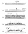
まず、第1基板1の製造プロセスを図8により説明する。
(1−a)第1基板(厚さ1mmのガラス基板)1の一方の面に、Crを厚さ1000Åでコーティングし遮光層10を形成し、所定部分からCrを除去して光通過部3を形成した(図8(a))。
(1−b)この上に厚さ1000ÅのSiO2層を形成した(図8(b))。
(1−c)さらに、厚さ1000ÅのITO(Indium Tin Oxide)層を形成した後、パターニングして第1基板1の電極7Aを形成した(図8(c))。なお、ITO層は透明である。
(1−d)厚さ3μmのポリイミドを形成しパターニングした。この後、熱処理することで、厚さ1.5μmのスペーサ8の一部を形成した(図8(d))。
【0041】
次に、第2基板2の製造プロセスを図9により説明する。
(2−a)第2基板(厚さ1mmのガラス基板)2の一方の面に、1000ÅのITOをコーティングした後、パターニングして電極7Bを形成した(図9(a))。
(2−b)レジストを1.5μm塗布し、第2基板のスペーサ8部分に穴を開けた(図9(b))。
(2−c)感光性のポリイミド(比誘電率が3程度のもの)を6μm塗布した(図9(c))。ここで用いるポリイミドは、黒色顔料を含浸させたものを用いた。
(2−d)パターニングにより、弾性部材6及び板材5を形成した(図9(d))。
(2−e)(2−b)で塗布したレジストを除去する。この後、熱処理することで、厚さ3μmのスペーサ8の一部を形成した(図9(e))。
【0042】
上記の第1基板1と第2基板2とを、各基板のスペーサ同士の位置合わせを行いつつ、向かい合わせに接合した。この後、スペーサにより形成される隙間内に比誘電率が25の液晶を注入した。第1基板1と第2基板との接合を、液晶中に浸漬させた状態で行うと、液晶注入を容易に行うことができる。
【0043】
【発明の効果】
本発明は上記のように構成したので、従来になく簡易な構成の、各種電磁波の二次元フィルタ、二次元光変調装置、二次元光演算装置等に応用される光変調装置を提供することができる。
また、陰極管ディスプレイと液晶ディスプレイの長所の多くを備えたディスプレイ装置を提供することができる。
【図面の簡単な説明】
【図1】本発明の光変調装置の一実施例を示す断面図であり(a)は光変調装置の側断面図、(b)はスペーサに弾性部材を介して板材が取り付けられた様子を示す平面図である。
【図2】(a),(b)はそれぞれ図1(a),(b)に対応する図であり、駆動電圧を所定の電圧としたときの板材の移動の様子を示すである。
【図3】本発明の光変調装置の他の実施例を示す図である。
【図4】複数の板材を直列に連結した実施例を示す図である。
【図5】1画素あたり3段の並列の板材群を示す図である。
【図6】遮光層を第2基板側に形成し、第1基板の全面に電極を形成し、この電極を1画素分機構単位で共用する実施例を示す図である。
【図7】遮光層を第2基板側に形成し、第1基板の全面に電極を形成し、この電極を複数の1画素分機構単位で共用する実施例を示す図である。
【図8】第1基板の製造プロセスの説明図である。
【図9】第2基板の製造プロセスの説明図である。
【符号の説明】
1 第1基板
2 第2基板
3 光通過部
4 隙間
5 板材
6 弾性支持体
6A,6B 弾性部材
7A,7B,7B′電極
8,8A,8B スペーサ
9 電源
10 遮光層
11 TFT
12 導光板
13 蛍光ランプ
111〜113 TFTの電極
141〜143 フィルタ素片[0001]
BACKGROUND OF THE INVENTION
The present invention relates to a light modulation device applied to various electromagnetic wave (including visible light, infrared light, and ultraviolet light) two-dimensional filters, two-dimensional light modulation devices, two-dimensional light arithmetic devices, and the like. The present invention relates to an applied display device.
[0002]
[Technical background]
Conventionally, a cathode ray tube display and a liquid crystal display are known as displays used in computers and the like. Cathode tube displays have the disadvantage that they occupy a large area and consume large amounts of power. For this reason, a thin and low power consumption type such as a liquid crystal display is expected to become the mainstream in the future. However, the liquid crystal display of the technical field of the present invention does not have the disadvantages of the above-mentioned cathode-ray tube display, but has a low contrast and a slow response speed (for example, in the case of a color TFT liquid crystal display, several tens to hundreds of milliseconds). In addition, there is a drawback that flicker is likely to occur.
[0003]
OBJECT OF THE INVENTION
An object of the present invention is to provide an optical modulation device that can be applied to a two-dimensional filter of electromagnetic waves, a two-dimensional light modulation device, a two-dimensional light calculation device, and the like.
Another object of the present invention is to provide a display capable of displaying a higher image quality while maintaining the thin and low power consumption characteristics of the liquid crystal display.
[0004]
SUMMARY OF THE INVENTION
The light modulation device of the present invention is configured to include a substrate pair composed of a first substrate and a second substrate arranged in parallel with a gap, and a plurality of light passing portions are provided on one or both substrates. A light shielding layer is formed.
[0005]
This light modulation device has a plate material made of a polymer material or the like provided for each light passage portion. This plate material usually serves as a shutter for shielding light. That is, the plate material changes the degree of overlap in the direction of each substrate surface with each light passing portion, so that light traveling from the second substrate side to the first substrate side, or from the second substrate side to the first substrate side Change the amount of light going to.
[0006]
A part or a plurality of parts of the elastic support are fixed to the substrate pair, and the other part or a plurality of parts of the elastic support support at least one of the plate members.
For example, the elastic support is composed of two elastic members, one end of each elastic member is fixed to the substrate pair, the other end of each elastic member is attached to one plate material, and each elastic member is arranged in a straight line. You can also. In this case, instead of the one plate material, a group of plate materials fixed to each other and arranged in series and / or in parallel in the linear direction may be attached to the elastic member. In addition, the number of elastic members constituting the elastic support can be appropriately increased. The elastic support generates a force that elastically returns the plate member or plate group to a mechanically stable position when the plate member or plate group moves by the action of a pair of electrodes described later.
The elastic member can be fixed to the substrate pair through a member such as a spacer provided between the first substrate and the second substrate, or the elastic member is directly attached to one surface of the plate member. You can also
[0007]
Each of the plate members applies a driving voltage (usually a unidirectional pulse) to a pair of electrodes (usually a pair of electrodes) formed on at least two of the elastic support, the first substrate, and the second substrate. Therefore, it moves by electrostatic force (electrostatic attractive force or electrostatic repulsive force). Thereby, the overlapping degree of a board | plate material and a light passage part changes. When the drive voltage is no longer applied to the set of electrodes, the plate material is elastically returned to a mechanically stable position by the elastic support. It should be noted that the degree of overlap is zero percent at the mechanically stable position of the plate material, and the degree of overlap increases (and eventually becomes 100 percent) when a driving voltage is applied to the one set of electrodes. In addition, the degree of overlap with the light passage portion of the plate material is 100% at the mechanically stable position of the plate material, and when the voltage is applied to the one set of electrodes, the degree of overlap decreases (finally zero). Can also be configured as a percentage).
[0008]
In the light modulation device of the present invention, both the first substrate and the second substrate may be transparent, and the light shielding layer may be formed on one or both of the first substrate and the second substrate. In this case, the amount of light passing through the light passage portion after passing through the second substrate or the first substrate toward the gap changes due to the movement of the plate material.
[0009]
In the light modulation device of the present invention, when the first substrate is transparent and the light shielding layer is formed on the first substrate, the light reflection layer can be formed on the surface of the second substrate on the gap side. In this case, due to the movement of the plate material, the amount of light reflected by the light reflecting layer after passing through the light passage portion toward the gap and passing through the light passage portion again changes.
The light reflecting layer can also be formed on the surface of the plate material on the first substrate side. In this case, a process that does not reflect light, such as forming a material layer with low light reflectance and light transmittance, is performed on the surface of the second substrate on the gap side.
[0010]
A liquid or gas can be sealed in the gap in consideration of an increase in electrostatic force or the like. A spacer can be used as a means for creating this gap.
Also, for example, for each mechanism unit (hereinafter referred to as “one-pixel mechanism unit”) for one pixel including the at least one plate member, the elastic support, and the one set of electrodes, It is also possible to isolate the gap in units of one pixel and to seal the liquid or gas into the isolated gap. In this case, it is also possible to use a spacer as the isolation means.
By enclosing a liquid or gas in the gap, the plate material can be moved with a small driving voltage. In this case, the resistivity of the plate material is 1010 Ω · cm or less, fluid resistivity is 107 It is preferable that the resistance of the fluid is at least Ω · cm, and the resistivity of the fluid is larger by one digit or more than the resistivity of the plate.
Conversely, even when the plate material is made of a dielectric material and the gap is made of a conductive material, the plate material can be electrostatically driven with a small voltage. In this case, the resistivity of the fluid is 1010 Ω · cm or less, and the resistivity of the plate is 107 It is preferable to set it to Ω · cm or more and to make the resistivity of the plate material one digit or more larger than the resistivity of the liquid.
[0011]
Further, the same effect as described above can be obtained when the plate material is made of a low dielectric constant material and a fluid with a high dielectric constant is sealed in the gap. Conversely, when the plate material is made of a high dielectric constant material and a low dielectric constant fluid is sealed in the gap, the same effect as described above can be obtained. In this case, the resistivity of the plate material and the fluid is 10 respectively.7 It is preferable to be Ω · cm or more.
[0012]
A device such as a monochrome or color display device or an overhead projector can be configured using the light modulation device. For example, a color display or the like can be configured by arranging filters of three primary colors of red, green, and blue on a first substrate or a second substrate in a matrix for each pixel unit.
[0013]
【Example】
Hereinafter, preferred embodiments of the present invention will be described.
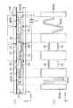
FIG. 1A is a side sectional view of the
In FIG. 1A, a
[0014]
The
[0015]
In addition, an
[0016]
The drive voltage Vd is usually a low voltage of 10 volts or less (preferably several volts or less). The drive voltage Vd is greatly influenced by the spring constants of the
The spring constants of the
On the other hand, the elastic modulus of organic polymer materials such as polyimide and PMMA (polymethyl methacrylate) is about two orders of magnitude smaller than that of ordinary inorganic materials. Therefore, in the manufacturing example described later, polyimide is used as the
[0017]
If the width of the
[0018]
Many fluids can be used as the sealing fluid L. A dielectric having a low relative dielectric constant of about 3 (for example, trade name Fluorinert Fluid) is used, and a dielectric having a high dielectric constant of 20 or more at room temperature (for example, water, ethanol, methanol, ethylene glycol, formamide) is also used. . In particular, many liquid crystal materials developed in recent years can be used. The sealed fluid L can also have an appropriate viscosity because of the necessity of damping when the
[0019]
Note that when a liquid having a low electrical resistivity such as water is used as the sealed fluid L, the leakage current increases. As a result, the holding time of the
It should be noted that a mixture of different liquids can be used to obtain the desired resistivity, relative dielectric constant, and viscosity.
[0020]
When a conductive material is used as the material of the
[0021]
FIG.1 (b) is a top view which shows a mode that the board |
When a drive voltage Vd (unidirectional pulse) is applied between the
[0022]
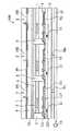
FIGS. 2A and 2B show states when the drive voltage Vd is a predetermined voltage, and correspond to FIGS. 1A and 1B where the drive voltage Vd is zero volts. . In this case, the
As described above, the amount of the incident light Bin that passes through the
[0023]
Although not shown, the
On the other hand, in the
[0024]
In the
[0025]
Alternatively, the
[0026]
Further, the
[0027]
FIGS. 3A to 3C are diagrams showing another embodiment of the light modulation device of the present invention. In the light modulation device of FIG. 3, the incident light Bin is reflected by the light reflecting layer formed on the second substrate 2 after passing through the
In the light modulation device shown in FIGS. 3A to 3C, the
In this light modulation device, the amount of reflected light (emitted light Bout) can be changed depending on the position of the
[0028]
In the light modulation device described above, in order to use the incident light Bin with high efficiency, the ratio (aperture ratio) of the occupied area of the
However, if the
In order to solve such a problem, a plurality of plate members (51, 52, 53 in the figure) can be connected in series as shown in FIG. In this case, the
[0029]
In the case of a high-precision display, the size of one pixel is about 200 μm × 200 μm. When the size of the
[0030]
The above series connection system has the following advantages. First, since the
[0031]
Furthermore, the serial connection method and the parallel connection method can coexist. In this case, it is desirable to employ a mechanism that restricts the movement of the plurality of plate members only in a desired direction (X direction in FIG. 1). For example, as shown in FIG. 5, three parallel
In FIG. 5, the
[0032]
Further, the aperture ratio becomes small for the following reason. That is, as shown in a manufacturing example described later, for example, the light modulation device in FIG. 1 includes a second substrate 2 on which a part of
Deviation occurs in the alignment at the time of joining. In particular, the deviation becomes larger as the display area of the light modulation device is larger. In order to cope with this shift, it is necessary to provide a margin for alignment with respect to the sizes of the
[0033]
In order to solve the above problem, the
[0034]
With the above-described structure, even if there is a positional shift between the
In addition, when the
[0035]
When the light modulation device of the present invention is applied to a display that displays a fixed pattern that displays only numbers, the number of necessary pixels is very small, so that each plate 5 (or plate group) is directly connected. It only has to be driven.
Further, when the light modulation device of the present invention is applied to a normal monochrome display or color display (that is, when each pixel is arranged in an array and an arbitrary pixel is accessed), the driving method is a TN liquid crystal display. This is basically the same as the matrix driving circuit used in FIG. For example, when the light modulation device of FIG. 1 is applied to a display, each
[0036]
In the case of a liquid crystal display, if a voltage in the same direction is continuously applied, an inverted AC voltage is used because the characteristics easily deteriorate. For this reason, the drive circuit becomes complicated and flicker is likely to occur. On the other hand, a display using the light modulation device of the present invention normally uses a unidirectional pulse, so that it does not easily deteriorate like a liquid crystal display, the drive circuit does not become complicated, and flicker does not easily occur. .
[0037]
The light modulation device described above can be applied to a monochrome display using ambient light such as room illumination light and natural light, or artificial light (backlight) as a light source, and a color display using artificial light.
In a monochrome display, two-dimensionally modulated transmitted or reflected light creates an image corresponding to the signal of the drive circuit.
In the color display, filter elements of light primary colors of red (R), green (G), and blue (B) are arranged in an array for each pixel on the surface of the
FIG. 7 is a diagram showing an example of a color display, and shows a state in which R, G, and
In addition, about the color filter formation method, since the technique used with the conventional color liquid crystal display can be employ | adopted, it does not elaborate.
[0038]
The light modulation device of the present invention can be applied to a projection display device such as an overhead projector by combining with the optical system.
[0039]
[Production example]
The light modulation apparatus described above can be easily realized by using a microlithography technique and, in some cases, a printing technique.
Hereinafter, a manufacturing process of an optical modulation device using a
[0040]
First, the manufacturing process of the
(1-a) On one surface of the first substrate (a glass substrate having a thickness of 1 mm), Cr is coated with a thickness of 1000 mm to form a
(1-b) 1000 Å thick SiO 22 A layer was formed (FIG. 8B).
(1-c) Further, an ITO (Indium Tin Oxide) layer having a thickness of 1000 mm was formed and then patterned to form an
(1-d) Polyimide having a thickness of 3 μm was formed and patterned. Thereafter, a part of the
[0041]
Next, the manufacturing process of the second substrate 2 will be described with reference to FIG.
(2-a) One side of the second substrate (glass substrate having a thickness of 1 mm) 2 was coated with 1000 ITO of ITO, and then patterned to form an
(2-b) 1.5 μm of resist was applied and a hole was made in the
(2-c) 6 μm of photosensitive polyimide (having a relative dielectric constant of about 3) was applied (FIG. 9C). The polyimide used here was impregnated with a black pigment.
(2-d) The
(2-e) The resist applied in (2-b) is removed. Thereafter, a part of the
[0042]
Said 1st board |
[0043]
【The invention's effect】
Since the present invention is configured as described above, it is possible to provide a light modulation device applied to various electromagnetic wave two-dimensional filters, two-dimensional light modulation devices, two-dimensional light calculation devices, etc., having a simpler structure than ever before. it can.
In addition, a display device having many of the advantages of a cathode ray tube display and a liquid crystal display can be provided.
[Brief description of the drawings]
FIG. 1 is a cross-sectional view showing an embodiment of a light modulation device of the present invention, (a) is a side cross-sectional view of the light modulation device, and (b) is a state where a plate material is attached to a spacer via an elastic member. FIG.
FIGS. 2A and 2B are diagrams corresponding to FIGS. 1A and 1B, respectively, showing a state of movement of a plate material when a driving voltage is set to a predetermined voltage.
FIG. 3 is a diagram showing another embodiment of the light modulation device of the present invention.
FIG. 4 is a view showing an embodiment in which a plurality of plate members are connected in series.
FIG. 5 is a diagram showing a group of three parallel plate members per pixel.
FIG. 6 is a diagram showing an embodiment in which a light shielding layer is formed on the second substrate side, an electrode is formed on the entire surface of the first substrate, and this electrode is shared in units of one pixel.
FIG. 7 is a diagram showing an embodiment in which a light shielding layer is formed on the second substrate side, an electrode is formed on the entire surface of the first substrate, and this electrode is shared by a plurality of one-pixel mechanism units.
FIG. 8 is an explanatory diagram of a manufacturing process of the first substrate.
FIG. 9 is an explanatory diagram of a manufacturing process of the second substrate.
[Explanation of symbols]
1 First substrate
2 Second substrate
3 Light passage
4 Clearance
5 Board material
6 Elastic support
6A, 6B Elastic member
7A, 7B, 7B 'electrode
8,8A, 8B Spacer
9 Power supply
10 Shading layer
11 TFT
12 Light guide plate
13 Fluorescent lamp
111-113 TFT electrodes
141-143 filter element
Claims (8)
Translated fromJapanese前記各光通過部ごとに設けられ、各光通過部との前記各基板の面方向の重なり度合いを変化させることで、前記第1基板側から前記第2基板側に向かう光の量、又は前記第2基板側から前記第1基板側に向かう光の量を変化させる、導電性高分子材料で形成された板材と、
一部分又は複数部分が前記基板対に対して固定され、他の一部分又は複数部分が前記板材の少なくとも1つを支持し、該少なくとも1つの板材を力学的安定位置に弾性復帰させる、有機高分子材料で形成された弾性支持体と、
前記弾性支持体、前記第1基板、前記第2基板のうちの少なくとも2つに形成され、前記重なり度合いが変化する向きに前記板材を静電力により移動させるための1組の電極と、を有し、
前記板材は前記各基板に平行にかつ前記面方向で移動するように配置され、前記弾性支持体は、前記板材の前記面方向の第1、第2の端部で該板材を支持するジグザグ状の第1、第2の部材を供え、該第1、第2の部材が該面方向に延伸して互いに逆に伸縮することを特徴とする光変調装置。A light-shielding layer is formed on either one or both substrates of a pair of substrates, each of which includes a first substrate and a second substrate arranged in parallel witha gapfilled with a liquid crystal material , leaving a plurality of light passing portions. A light modulator,
An amount of light traveling from the first substrate side to the second substrate side by changing the degree of overlap inthe surface direction of each substrate with each light passage unit provided for each light passage unit, orA plateformed of a conductive polymer material that changes the amount of light traveling from the second substrate side toward the first substrate side;
Anorganic polymer material in which a part or a plurality of parts are fixed to the substrate pair, and the other part or a plurality of parts support at least one of the plates, and elastically return the at least one plate to a mechanically stable position.An elastic supportformed of
A pair of electrodes formed on at least two of the elastic support, the first substrate, and the second substrate for moving the plate by electrostatic force in a direction in which the degree of overlap changes. And
The plate material is arranged so as to move in parallel to the respective substrates and in the surface direction, and the elastic support is a zigzag shape that supports the plate material at first and second end portions in the surface direction of the plate material. A light modulation device comprising: the first and second members, wherein the first and second members extend in the plane direction and expand and contract in opposite directions.
Priority Applications (4)
| Application Number | Priority Date | Filing Date | Title |
|---|---|---|---|
| JP35261595AJP3799092B2 (en) | 1995-12-29 | 1995-12-29 | Light modulation device and display device |
| US08/771,566US5745281A (en) | 1995-12-29 | 1996-12-20 | Electrostatically-driven light modulator and display |
| EP96309485AEP0786679A3 (en) | 1995-12-29 | 1996-12-24 | Electrostatically-driven light modulator and display |
| KR1019960075231AKR970048702A (en) | 1995-12-29 | 1996-12-28 | Capacitive Drive Optical Modulation Devices and Displays |
Applications Claiming Priority (1)
| Application Number | Priority Date | Filing Date | Title |
|---|---|---|---|
| JP35261595AJP3799092B2 (en) | 1995-12-29 | 1995-12-29 | Light modulation device and display device |
Publications (2)
| Publication Number | Publication Date |
|---|---|
| JPH09189869A JPH09189869A (en) | 1997-07-22 |
| JP3799092B2true JP3799092B2 (en) | 2006-07-19 |
Family
ID=18425264
Family Applications (1)
| Application Number | Title | Priority Date | Filing Date |
|---|---|---|---|
| JP35261595AExpired - Fee RelatedJP3799092B2 (en) | 1995-12-29 | 1995-12-29 | Light modulation device and display device |
Country Status (4)
| Country | Link |
|---|---|
| US (1) | US5745281A (en) |
| EP (1) | EP0786679A3 (en) |
| JP (1) | JP3799092B2 (en) |
| KR (1) | KR970048702A (en) |
Families Citing this family (280)
| Publication number | Priority date | Publication date | Assignee | Title |
|---|---|---|---|---|
| US6674562B1 (en)* | 1994-05-05 | 2004-01-06 | Iridigm Display Corporation | Interferometric modulation of radiation |
| US7123216B1 (en) | 1994-05-05 | 2006-10-17 | Idc, Llc | Photonic MEMS and structures |
| US7297471B1 (en) | 2003-04-15 | 2007-11-20 | Idc, Llc | Method for manufacturing an array of interferometric modulators |
| US8014059B2 (en)* | 1994-05-05 | 2011-09-06 | Qualcomm Mems Technologies, Inc. | System and method for charge control in a MEMS device |
| US7138984B1 (en) | 2001-06-05 | 2006-11-21 | Idc, Llc | Directly laminated touch sensitive screen |
| US7550794B2 (en) | 2002-09-20 | 2009-06-23 | Idc, Llc | Micromechanical systems device comprising a displaceable electrode and a charge-trapping layer |
| US7460291B2 (en) | 1994-05-05 | 2008-12-02 | Idc, Llc | Separable modulator |
| US6680792B2 (en)* | 1994-05-05 | 2004-01-20 | Iridigm Display Corporation | Interferometric modulation of radiation |
| US7006661B2 (en)* | 1995-07-27 | 2006-02-28 | Digimarc Corp | Digital watermarking systems and methods |
| US7907319B2 (en)* | 1995-11-06 | 2011-03-15 | Qualcomm Mems Technologies, Inc. | Method and device for modulating light with optical compensation |
| JP4433335B2 (en)* | 1996-04-17 | 2010-03-17 | ディーコン アクティー ゼルスカブ | Method and apparatus for controlling light |
| US7471444B2 (en)* | 1996-12-19 | 2008-12-30 | Idc, Llc | Interferometric modulation of radiation |
| US7532377B2 (en) | 1998-04-08 | 2009-05-12 | Idc, Llc | Movable micro-electromechanical device |
| WO1999052006A2 (en) | 1998-04-08 | 1999-10-14 | Etalon, Inc. | Interferometric modulation of radiation |
| US8928967B2 (en) | 1998-04-08 | 2015-01-06 | Qualcomm Mems Technologies, Inc. | Method and device for modulating light |
| EP0994373A1 (en)* | 1998-09-18 | 2000-04-19 | Ngk Insulators, Ltd. | Display device comprising actuators |
| JP4074714B2 (en)* | 1998-09-25 | 2008-04-09 | 富士フイルム株式会社 | Array type light modulation element and flat display driving method |
| JP3919954B2 (en)* | 1998-10-16 | 2007-05-30 | 富士フイルム株式会社 | Array type light modulation element and flat display driving method |
| US6288824B1 (en)* | 1998-11-03 | 2001-09-11 | Alex Kastalsky | Display device based on grating electromechanical shutter |
| US6191883B1 (en)* | 1998-12-30 | 2001-02-20 | Texas Instruments Incorporated | Five transistor SRAM cell for small micromirror elements |
| US6859299B1 (en) | 1999-06-11 | 2005-02-22 | Jung-Chih Chiao | MEMS optical components |
| US6275320B1 (en)* | 1999-09-27 | 2001-08-14 | Jds Uniphase, Inc. | MEMS variable optical attenuator |
| WO2003007049A1 (en) | 1999-10-05 | 2003-01-23 | Iridigm Display Corporation | Photonic mems and structures |
| US6538796B1 (en)* | 2000-03-31 | 2003-03-25 | The United States Of America As Represented By The Administrator Of The National Aeronautics And Space Administration | MEMS device for spacecraft thermal control applications |
| KR100368637B1 (en)* | 2000-05-15 | 2003-01-24 | (주)해라시스템 | Flat Panel Display using Microelectromchanical System Devices |
| AU2000273447A1 (en)* | 2000-06-09 | 2001-12-24 | University Of Hawaii | Mems optical components |
| US6962771B1 (en)* | 2000-10-13 | 2005-11-08 | Taiwan Semiconductor Manufacturing Company, Ltd. | Dual damascene process |
| JP3646250B2 (en)* | 2000-11-15 | 2005-05-11 | 日本航空電子工業株式会社 | Light switch |
| US6495944B2 (en) | 2001-04-18 | 2002-12-17 | International Business Machines Corporation | Electrostatic microactuator with viscous liquid damping |
| US6589625B1 (en) | 2001-08-01 | 2003-07-08 | Iridigm Display Corporation | Hermetic seal and method to create the same |
| US6574032B1 (en)* | 2002-01-23 | 2003-06-03 | Eastman Kodak Company | Imaging apparatus using dither to minimize pixel effects |
| US6794119B2 (en) | 2002-02-12 | 2004-09-21 | Iridigm Display Corporation | Method for fabricating a structure for a microelectromechanical systems (MEMS) device |
| US6574033B1 (en) | 2002-02-27 | 2003-06-03 | Iridigm Display Corporation | Microelectromechanical systems device and method for fabricating same |
| US6972882B2 (en)* | 2002-04-30 | 2005-12-06 | Hewlett-Packard Development Company, L.P. | Micro-mirror device with light angle amplification |
| US20030202264A1 (en)* | 2002-04-30 | 2003-10-30 | Weber Timothy L. | Micro-mirror device |
| US7023603B2 (en)* | 2002-04-30 | 2006-04-04 | Hewlett-Packard Development Company, L.P. | Micro-mirror device including dielectrophoretic microemulsion |
| US6954297B2 (en)* | 2002-04-30 | 2005-10-11 | Hewlett-Packard Development Company, L.P. | Micro-mirror device including dielectrophoretic liquid |
| US6667823B2 (en)* | 2002-05-22 | 2003-12-23 | Lucent Technologies Inc. | Monolithic in-plane shutter switch |
| US7781850B2 (en) | 2002-09-20 | 2010-08-24 | Qualcomm Mems Technologies, Inc. | Controlling electromechanical behavior of structures within a microelectromechanical systems device |
| KR20070044072A (en)* | 2002-10-18 | 2007-04-26 | 키네토 와이어리즈 인코포레이션 | Apparatus and method for extending coverage area of licensed wireless communication system using unlicensed wireless communication system |
| TWI289708B (en) | 2002-12-25 | 2007-11-11 | Qualcomm Mems Technologies Inc | Optical interference type color display |
| TW200413810A (en) | 2003-01-29 | 2004-08-01 | Prime View Int Co Ltd | Light interference display panel and its manufacturing method |
| US6903487B2 (en)* | 2003-02-14 | 2005-06-07 | Hewlett-Packard Development Company, L.P. | Micro-mirror device with increased mirror tilt |
| US7417782B2 (en)* | 2005-02-23 | 2008-08-26 | Pixtronix, Incorporated | Methods and apparatus for spatial light modulation |
| US6917462B2 (en)* | 2003-02-24 | 2005-07-12 | Eastman Kodak Company | Method and apparatus for translating a spatial light modulator to provide dithering |
| US6844953B2 (en)* | 2003-03-12 | 2005-01-18 | Hewlett-Packard Development Company, L.P. | Micro-mirror device including dielectrophoretic liquid |
| US6993219B2 (en)* | 2003-03-13 | 2006-01-31 | Lucent Technologies Inc. | Waveguide/MEMS switch |
| US6876484B2 (en) | 2003-03-24 | 2005-04-05 | Lucent Technologies Inc. | Deformable segmented MEMS mirror |
| TW594360B (en) | 2003-04-21 | 2004-06-21 | Prime View Int Corp Ltd | A method for fabricating an interference display cell |
| JP4338442B2 (en)* | 2003-05-23 | 2009-10-07 | 富士フイルム株式会社 | Manufacturing method of transmissive light modulation element |
| TW570896B (en) | 2003-05-26 | 2004-01-11 | Prime View Int Co Ltd | A method for fabricating an interference display cell |
| US6989920B2 (en)* | 2003-05-29 | 2006-01-24 | Asml Holding N.V. | System and method for dose control in a lithographic system |
| US7061591B2 (en)* | 2003-05-30 | 2006-06-13 | Asml Holding N.V. | Maskless lithography systems and methods utilizing spatial light modulator arrays |
| US7221495B2 (en)* | 2003-06-24 | 2007-05-22 | Idc Llc | Thin film precursor stack for MEMS manufacturing |
| TWI231865B (en) | 2003-08-26 | 2005-05-01 | Prime View Int Co Ltd | An interference display cell and fabrication method thereof |
| TW593126B (en)* | 2003-09-30 | 2004-06-21 | Prime View Int Co Ltd | A structure of a micro electro mechanical system and manufacturing the same |
| US6894824B2 (en)* | 2003-10-02 | 2005-05-17 | Hewlett-Packard Development Company, L.P. | Micro mirror device with spring and method for the same |
| US7012726B1 (en) | 2003-11-03 | 2006-03-14 | Idc, Llc | MEMS devices with unreleased thin film components |
| US7161728B2 (en)* | 2003-12-09 | 2007-01-09 | Idc, Llc | Area array modulation and lead reduction in interferometric modulators |
| US7142346B2 (en)* | 2003-12-09 | 2006-11-28 | Idc, Llc | System and method for addressing a MEMS display |
| US6917456B2 (en)* | 2003-12-09 | 2005-07-12 | Hewlett-Packard Development Company, L.P. | Light modulator |
| US7532194B2 (en)* | 2004-02-03 | 2009-05-12 | Idc, Llc | Driver voltage adjuster |
| US7342705B2 (en) | 2004-02-03 | 2008-03-11 | Idc, Llc | Spatial light modulator with integrated optical compensation structure |
| US7119945B2 (en) | 2004-03-03 | 2006-10-10 | Idc, Llc | Altering temporal response of microelectromechanical elements |
| US6999228B2 (en)* | 2004-03-05 | 2006-02-14 | Hewlett-Packard Development Company, L.P. | Micro mirror device with adjacently suspended spring and method for the same |
| US7706050B2 (en) | 2004-03-05 | 2010-04-27 | Qualcomm Mems Technologies, Inc. | Integrated modulator illumination |
| US7855824B2 (en)* | 2004-03-06 | 2010-12-21 | Qualcomm Mems Technologies, Inc. | Method and system for color optimization in a display |
| US7720148B2 (en)* | 2004-03-26 | 2010-05-18 | The Hong Kong University Of Science And Technology | Efficient multi-frame motion estimation for video compression |
| US7476327B2 (en) | 2004-05-04 | 2009-01-13 | Idc, Llc | Method of manufacture for microelectromechanical devices |
| US7060895B2 (en)* | 2004-05-04 | 2006-06-13 | Idc, Llc | Modifying the electro-mechanical behavior of devices |
| US7164520B2 (en)* | 2004-05-12 | 2007-01-16 | Idc, Llc | Packaging for an interferometric modulator |
| US7256922B2 (en)* | 2004-07-02 | 2007-08-14 | Idc, Llc | Interferometric modulators with thin film transistors |
| EP2246726B1 (en) | 2004-07-29 | 2013-04-03 | QUALCOMM MEMS Technologies, Inc. | System and method for micro-electromechanical operating of an interferometric modulator |
| US7515147B2 (en) | 2004-08-27 | 2009-04-07 | Idc, Llc | Staggered column drive circuit systems and methods |
| US7499208B2 (en) | 2004-08-27 | 2009-03-03 | Udc, Llc | Current mode display driver circuit realization feature |
| US7560299B2 (en)* | 2004-08-27 | 2009-07-14 | Idc, Llc | Systems and methods of actuating MEMS display elements |
| US7551159B2 (en) | 2004-08-27 | 2009-06-23 | Idc, Llc | System and method of sensing actuation and release voltages of an interferometric modulator |
| US7889163B2 (en)* | 2004-08-27 | 2011-02-15 | Qualcomm Mems Technologies, Inc. | Drive method for MEMS devices |
| US7623142B2 (en)* | 2004-09-14 | 2009-11-24 | Hewlett-Packard Development Company, L.P. | Flexure |
| US7602375B2 (en)* | 2004-09-27 | 2009-10-13 | Idc, Llc | Method and system for writing data to MEMS display elements |
| US7554714B2 (en) | 2004-09-27 | 2009-06-30 | Idc, Llc | Device and method for manipulation of thermal response in a modulator |
| US7321456B2 (en) | 2004-09-27 | 2008-01-22 | Idc, Llc | Method and device for corner interferometric modulation |
| US7920135B2 (en) | 2004-09-27 | 2011-04-05 | Qualcomm Mems Technologies, Inc. | Method and system for driving a bi-stable display |
| US7675669B2 (en) | 2004-09-27 | 2010-03-09 | Qualcomm Mems Technologies, Inc. | Method and system for driving interferometric modulators |
| US7460246B2 (en) | 2004-09-27 | 2008-12-02 | Idc, Llc | Method and system for sensing light using interferometric elements |
| US7429334B2 (en) | 2004-09-27 | 2008-09-30 | Idc, Llc | Methods of fabricating interferometric modulators by selectively removing a material |
| US7259449B2 (en)* | 2004-09-27 | 2007-08-21 | Idc, Llc | Method and system for sealing a substrate |
| US7369294B2 (en) | 2004-09-27 | 2008-05-06 | Idc, Llc | Ornamental display device |
| US7373026B2 (en) | 2004-09-27 | 2008-05-13 | Idc, Llc | MEMS device fabricated on a pre-patterned substrate |
| US7492502B2 (en) | 2004-09-27 | 2009-02-17 | Idc, Llc | Method of fabricating a free-standing microstructure |
| US7692839B2 (en)* | 2004-09-27 | 2010-04-06 | Qualcomm Mems Technologies, Inc. | System and method of providing MEMS device with anti-stiction coating |
| US7807488B2 (en)* | 2004-09-27 | 2010-10-05 | Qualcomm Mems Technologies, Inc. | Display element having filter material diffused in a substrate of the display element |
| US7349136B2 (en) | 2004-09-27 | 2008-03-25 | Idc, Llc | Method and device for a display having transparent components integrated therein |
| US7719500B2 (en) | 2004-09-27 | 2010-05-18 | Qualcomm Mems Technologies, Inc. | Reflective display pixels arranged in non-rectangular arrays |
| US20060176487A1 (en)* | 2004-09-27 | 2006-08-10 | William Cummings | Process control monitors for interferometric modulators |
| US7424198B2 (en) | 2004-09-27 | 2008-09-09 | Idc, Llc | Method and device for packaging a substrate |
| US7355780B2 (en) | 2004-09-27 | 2008-04-08 | Idc, Llc | System and method of illuminating interferometric modulators using backlighting |
| US8362987B2 (en)* | 2004-09-27 | 2013-01-29 | Qualcomm Mems Technologies, Inc. | Method and device for manipulating color in a display |
| US7808703B2 (en)* | 2004-09-27 | 2010-10-05 | Qualcomm Mems Technologies, Inc. | System and method for implementation of interferometric modulator displays |
| US8124434B2 (en) | 2004-09-27 | 2012-02-28 | Qualcomm Mems Technologies, Inc. | Method and system for packaging a display |
| US7710629B2 (en)* | 2004-09-27 | 2010-05-04 | Qualcomm Mems Technologies, Inc. | System and method for display device with reinforcing substance |
| US20060066594A1 (en)* | 2004-09-27 | 2006-03-30 | Karen Tyger | Systems and methods for driving a bi-stable display element |
| US7911428B2 (en)* | 2004-09-27 | 2011-03-22 | Qualcomm Mems Technologies, Inc. | Method and device for manipulating color in a display |
| US7372613B2 (en) | 2004-09-27 | 2008-05-13 | Idc, Llc | Method and device for multistate interferometric light modulation |
| US8878825B2 (en) | 2004-09-27 | 2014-11-04 | Qualcomm Mems Technologies, Inc. | System and method for providing a variable refresh rate of an interferometric modulator display |
| US7724993B2 (en)* | 2004-09-27 | 2010-05-25 | Qualcomm Mems Technologies, Inc. | MEMS switches with deforming membranes |
| US7916103B2 (en)* | 2004-09-27 | 2011-03-29 | Qualcomm Mems Technologies, Inc. | System and method for display device with end-of-life phenomena |
| US7417735B2 (en) | 2004-09-27 | 2008-08-26 | Idc, Llc | Systems and methods for measuring color and contrast in specular reflective devices |
| US7626581B2 (en) | 2004-09-27 | 2009-12-01 | Idc, Llc | Device and method for display memory using manipulation of mechanical response |
| US7701631B2 (en) | 2004-09-27 | 2010-04-20 | Qualcomm Mems Technologies, Inc. | Device having patterned spacers for backplates and method of making the same |
| US7302157B2 (en) | 2004-09-27 | 2007-11-27 | Idc, Llc | System and method for multi-level brightness in interferometric modulation |
| US7928928B2 (en)* | 2004-09-27 | 2011-04-19 | Qualcomm Mems Technologies, Inc. | Apparatus and method for reducing perceived color shift |
| US7653371B2 (en) | 2004-09-27 | 2010-01-26 | Qualcomm Mems Technologies, Inc. | Selectable capacitance circuit |
| US7453579B2 (en) | 2004-09-27 | 2008-11-18 | Idc, Llc | Measurement of the dynamic characteristics of interferometric modulators |
| US7710632B2 (en)* | 2004-09-27 | 2010-05-04 | Qualcomm Mems Technologies, Inc. | Display device having an array of spatial light modulators with integrated color filters |
| US7369296B2 (en)* | 2004-09-27 | 2008-05-06 | Idc, Llc | Device and method for modifying actuation voltage thresholds of a deformable membrane in an interferometric modulator |
| US7944599B2 (en) | 2004-09-27 | 2011-05-17 | Qualcomm Mems Technologies, Inc. | Electromechanical device with optical function separated from mechanical and electrical function |
| US7343080B2 (en) | 2004-09-27 | 2008-03-11 | Idc, Llc | System and method of testing humidity in a sealed MEMS device |
| AU2005289445A1 (en)* | 2004-09-27 | 2006-04-06 | Idc, Llc | Method and device for multistate interferometric light modulation |
| US7345805B2 (en)* | 2004-09-27 | 2008-03-18 | Idc, Llc | Interferometric modulator array with integrated MEMS electrical switches |
| US20060077126A1 (en)* | 2004-09-27 | 2006-04-13 | Manish Kothari | Apparatus and method for arranging devices into an interconnected array |
| US7317568B2 (en) | 2004-09-27 | 2008-01-08 | Idc, Llc | System and method of implementation of interferometric modulators for display mirrors |
| US7893919B2 (en) | 2004-09-27 | 2011-02-22 | Qualcomm Mems Technologies, Inc. | Display region architectures |
| US7532195B2 (en)* | 2004-09-27 | 2009-05-12 | Idc, Llc | Method and system for reducing power consumption in a display |
| US7359066B2 (en)* | 2004-09-27 | 2008-04-15 | Idc, Llc | Electro-optical measurement of hysteresis in interferometric modulators |
| US7936497B2 (en) | 2004-09-27 | 2011-05-03 | Qualcomm Mems Technologies, Inc. | MEMS device having deformable membrane characterized by mechanical persistence |
| US7130104B2 (en)* | 2004-09-27 | 2006-10-31 | Idc, Llc | Methods and devices for inhibiting tilting of a mirror in an interferometric modulator |
| US7684104B2 (en)* | 2004-09-27 | 2010-03-23 | Idc, Llc | MEMS using filler material and method |
| US8310441B2 (en) | 2004-09-27 | 2012-11-13 | Qualcomm Mems Technologies, Inc. | Method and system for writing data to MEMS display elements |
| US7420725B2 (en) | 2004-09-27 | 2008-09-02 | Idc, Llc | Device having a conductive light absorbing mask and method for fabricating same |
| US20060103643A1 (en)* | 2004-09-27 | 2006-05-18 | Mithran Mathew | Measuring and modeling power consumption in displays |
| US7630119B2 (en) | 2004-09-27 | 2009-12-08 | Qualcomm Mems Technologies, Inc. | Apparatus and method for reducing slippage between structures in an interferometric modulator |
| US7668415B2 (en)* | 2004-09-27 | 2010-02-23 | Qualcomm Mems Technologies, Inc. | Method and device for providing electronic circuitry on a backplate |
| US7843410B2 (en)* | 2004-09-27 | 2010-11-30 | Qualcomm Mems Technologies, Inc. | Method and device for electrically programmable display |
| US7289256B2 (en)* | 2004-09-27 | 2007-10-30 | Idc, Llc | Electrical characterization of interferometric modulators |
| US7327510B2 (en) | 2004-09-27 | 2008-02-05 | Idc, Llc | Process for modifying offset voltage characteristics of an interferometric modulator |
| US7545550B2 (en)* | 2004-09-27 | 2009-06-09 | Idc, Llc | Systems and methods of actuating MEMS display elements |
| US7417783B2 (en) | 2004-09-27 | 2008-08-26 | Idc, Llc | Mirror and mirror layer for optical modulator and method |
| US8008736B2 (en) | 2004-09-27 | 2011-08-30 | Qualcomm Mems Technologies, Inc. | Analog interferometric modulator device |
| US7813026B2 (en)* | 2004-09-27 | 2010-10-12 | Qualcomm Mems Technologies, Inc. | System and method of reducing color shift in a display |
| US7299681B2 (en)* | 2004-09-27 | 2007-11-27 | Idc, Llc | Method and system for detecting leak in electronic devices |
| US7304784B2 (en) | 2004-09-27 | 2007-12-04 | Idc, Llc | Reflective display device having viewable display on both sides |
| US7446927B2 (en)* | 2004-09-27 | 2008-11-04 | Idc, Llc | MEMS switch with set and latch electrodes |
| US7161730B2 (en) | 2004-09-27 | 2007-01-09 | Idc, Llc | System and method for providing thermal compensation for an interferometric modulator display |
| US7679627B2 (en) | 2004-09-27 | 2010-03-16 | Qualcomm Mems Technologies, Inc. | Controller and driver features for bi-stable display |
| US20060066557A1 (en)* | 2004-09-27 | 2006-03-30 | Floyd Philip D | Method and device for reflective display with time sequential color illumination |
| US7415186B2 (en)* | 2004-09-27 | 2008-08-19 | Idc, Llc | Methods for visually inspecting interferometric modulators for defects |
| US7310179B2 (en) | 2004-09-27 | 2007-12-18 | Idc, Llc | Method and device for selective adjustment of hysteresis window |
| US7405924B2 (en) | 2004-09-27 | 2008-07-29 | Idc, Llc | System and method for protecting microelectromechanical systems array using structurally reinforced back-plate |
| US7586484B2 (en)* | 2004-09-27 | 2009-09-08 | Idc, Llc | Controller and driver features for bi-stable display |
| US7289259B2 (en) | 2004-09-27 | 2007-10-30 | Idc, Llc | Conductive bus structure for interferometric modulator array |
| US7553684B2 (en) | 2004-09-27 | 2009-06-30 | Idc, Llc | Method of fabricating interferometric devices using lift-off processing techniques |
| US7535466B2 (en) | 2004-09-27 | 2009-05-19 | Idc, Llc | System with server based control of client device display features |
| US7527995B2 (en) | 2004-09-27 | 2009-05-05 | Qualcomm Mems Technologies, Inc. | Method of making prestructure for MEMS systems |
| US20060076634A1 (en)* | 2004-09-27 | 2006-04-13 | Lauren Palmateer | Method and system for packaging MEMS devices with incorporated getter |
| US7136213B2 (en)* | 2004-09-27 | 2006-11-14 | Idc, Llc | Interferometric modulators having charge persistence |
| US7564612B2 (en) | 2004-09-27 | 2009-07-21 | Idc, Llc | Photonic MEMS and structures |
| US7583429B2 (en) | 2004-09-27 | 2009-09-01 | Idc, Llc | Ornamental display device |
| US7368803B2 (en)* | 2004-09-27 | 2008-05-06 | Idc, Llc | System and method for protecting microelectromechanical systems array using back-plate with non-flat portion |
| US7898521B2 (en)* | 2004-09-27 | 2011-03-01 | Qualcomm Mems Technologies, Inc. | Device and method for wavelength filtering |
| US7405861B2 (en) | 2004-09-27 | 2008-07-29 | Idc, Llc | Method and device for protecting interferometric modulators from electrostatic discharge |
| US7184193B2 (en)* | 2004-10-05 | 2007-02-27 | Hewlett-Packard Development Company, L.P. | Systems and methods for amorphous flexures in micro-electro mechanical systems |
| TW200628877A (en) | 2005-02-04 | 2006-08-16 | Prime View Int Co Ltd | Method of manufacturing optical interference type color display |
| CA2795302C (en)* | 2005-02-23 | 2015-06-23 | Pixtronix, Inc. | Methods and apparatus for actuating displays |
| US8482496B2 (en) | 2006-01-06 | 2013-07-09 | Pixtronix, Inc. | Circuits for controlling MEMS display apparatus on a transparent substrate |
| US7502159B2 (en)* | 2005-02-23 | 2009-03-10 | Pixtronix, Inc. | Methods and apparatus for actuating displays |
| US7742016B2 (en) | 2005-02-23 | 2010-06-22 | Pixtronix, Incorporated | Display methods and apparatus |
| US7999994B2 (en) | 2005-02-23 | 2011-08-16 | Pixtronix, Inc. | Display apparatus and methods for manufacture thereof |
| US8159428B2 (en) | 2005-02-23 | 2012-04-17 | Pixtronix, Inc. | Display methods and apparatus |
| US7304785B2 (en)* | 2005-02-23 | 2007-12-04 | Pixtronix, Inc. | Display methods and apparatus |
| US20080158635A1 (en)* | 2005-02-23 | 2008-07-03 | Pixtronix, Inc. | Display apparatus and methods for manufacture thereof |
| US9229222B2 (en) | 2005-02-23 | 2016-01-05 | Pixtronix, Inc. | Alignment methods in fluid-filled MEMS displays |
| US7304786B2 (en) | 2005-02-23 | 2007-12-04 | Pixtronix, Inc. | Methods and apparatus for bi-stable actuation of displays |
| US9087486B2 (en) | 2005-02-23 | 2015-07-21 | Pixtronix, Inc. | Circuits for controlling display apparatus |
| CN102060258B (en)* | 2005-02-23 | 2013-07-10 | 皮克斯特隆尼斯有限公司 | Microelectronic mechanical shutter device |
| US8519945B2 (en) | 2006-01-06 | 2013-08-27 | Pixtronix, Inc. | Circuits for controlling display apparatus |
| US7746529B2 (en)* | 2005-02-23 | 2010-06-29 | Pixtronix, Inc. | MEMS display apparatus |
| US7755582B2 (en) | 2005-02-23 | 2010-07-13 | Pixtronix, Incorporated | Display methods and apparatus |
| US8310442B2 (en)* | 2005-02-23 | 2012-11-13 | Pixtronix, Inc. | Circuits for controlling display apparatus |
| BRPI0607879A2 (en)* | 2005-02-23 | 2009-10-20 | Pixtronix Inc | visualization apparatus and method of forming an image in a visualization device |
| US9082353B2 (en) | 2010-01-05 | 2015-07-14 | Pixtronix, Inc. | Circuits for controlling display apparatus |
| US7675665B2 (en) | 2005-02-23 | 2010-03-09 | Pixtronix, Incorporated | Methods and apparatus for actuating displays |
| US20070205969A1 (en) | 2005-02-23 | 2007-09-06 | Pixtronix, Incorporated | Direct-view MEMS display devices and methods for generating images thereon |
| US9158106B2 (en) | 2005-02-23 | 2015-10-13 | Pixtronix, Inc. | Display methods and apparatus |
| US9261694B2 (en) | 2005-02-23 | 2016-02-16 | Pixtronix, Inc. | Display apparatus and methods for manufacture thereof |
| EP1878001A1 (en) | 2005-05-05 | 2008-01-16 | QUALCOMM Incorporated, Inc. | Dynamic driver ic and display panel configuration |
| US7948457B2 (en) | 2005-05-05 | 2011-05-24 | Qualcomm Mems Technologies, Inc. | Systems and methods of actuating MEMS display elements |
| US7920136B2 (en)* | 2005-05-05 | 2011-04-05 | Qualcomm Mems Technologies, Inc. | System and method of driving a MEMS display device |
| US20060277486A1 (en)* | 2005-06-02 | 2006-12-07 | Skinner David N | File or user interface element marking system |
| EP2495212A3 (en)* | 2005-07-22 | 2012-10-31 | QUALCOMM MEMS Technologies, Inc. | Mems devices having support structures and methods of fabricating the same |
| KR20080041663A (en) | 2005-07-22 | 2008-05-13 | 콸콤 인코포레이티드 | Supporting structures for MEMS devices and methods thereof |
| KR101375337B1 (en)* | 2005-07-22 | 2014-03-18 | 퀄컴 엠이엠에스 테크놀로지스, 인크. | Electomechanical devices having support structures and methods of fabricating the same |
| CN101228091A (en)* | 2005-07-22 | 2008-07-23 | 高通股份有限公司 | Support structures and methods for MEMS devices |
| US7355779B2 (en)* | 2005-09-02 | 2008-04-08 | Idc, Llc | Method and system for driving MEMS display elements |
| US7630114B2 (en) | 2005-10-28 | 2009-12-08 | Idc, Llc | Diffusion barrier layer for MEMS devices |
| WO2007075832A2 (en)* | 2005-12-19 | 2007-07-05 | Pixtronix, Inc. | Direct-view mems display devices and methods for generating images thereon |
| US8391630B2 (en)* | 2005-12-22 | 2013-03-05 | Qualcomm Mems Technologies, Inc. | System and method for power reduction when decompressing video streams for interferometric modulator displays |
| US7795061B2 (en) | 2005-12-29 | 2010-09-14 | Qualcomm Mems Technologies, Inc. | Method of creating MEMS device cavities by a non-etching process |
| US7636151B2 (en)* | 2006-01-06 | 2009-12-22 | Qualcomm Mems Technologies, Inc. | System and method for providing residual stress test structures |
| US7916980B2 (en) | 2006-01-13 | 2011-03-29 | Qualcomm Mems Technologies, Inc. | Interconnect structure for MEMS device |
| US7382515B2 (en) | 2006-01-18 | 2008-06-03 | Qualcomm Mems Technologies, Inc. | Silicon-rich silicon nitrides as etch stops in MEMS manufacture |
| US8194056B2 (en) | 2006-02-09 | 2012-06-05 | Qualcomm Mems Technologies Inc. | Method and system for writing data to MEMS display elements |
| US7582952B2 (en) | 2006-02-21 | 2009-09-01 | Qualcomm Mems Technologies, Inc. | Method for providing and removing discharging interconnect for chip-on-glass output leads and structures thereof |
| US7547568B2 (en) | 2006-02-22 | 2009-06-16 | Qualcomm Mems Technologies, Inc. | Electrical conditioning of MEMS device and insulating layer thereof |
| US7550810B2 (en) | 2006-02-23 | 2009-06-23 | Qualcomm Mems Technologies, Inc. | MEMS device having a layer movable at asymmetric rates |
| US8526096B2 (en) | 2006-02-23 | 2013-09-03 | Pixtronix, Inc. | Mechanical light modulators with stressed beams |
| US7450295B2 (en) | 2006-03-02 | 2008-11-11 | Qualcomm Mems Technologies, Inc. | Methods for producing MEMS with protective coatings using multi-component sacrificial layers |
| US7643203B2 (en) | 2006-04-10 | 2010-01-05 | Qualcomm Mems Technologies, Inc. | Interferometric optical display system with broadband characteristics |
| US7903047B2 (en) | 2006-04-17 | 2011-03-08 | Qualcomm Mems Technologies, Inc. | Mode indicator for interferometric modulator displays |
| US7527996B2 (en) | 2006-04-19 | 2009-05-05 | Qualcomm Mems Technologies, Inc. | Non-planar surface structures and process for microelectromechanical systems |
| US7711239B2 (en) | 2006-04-19 | 2010-05-04 | Qualcomm Mems Technologies, Inc. | Microelectromechanical device and method utilizing nanoparticles |
| US7417784B2 (en) | 2006-04-19 | 2008-08-26 | Qualcomm Mems Technologies, Inc. | Microelectromechanical device and method utilizing a porous surface |
| US7623287B2 (en) | 2006-04-19 | 2009-11-24 | Qualcomm Mems Technologies, Inc. | Non-planar surface structures and process for microelectromechanical systems |
| US8004743B2 (en)* | 2006-04-21 | 2011-08-23 | Qualcomm Mems Technologies, Inc. | Method and apparatus for providing brightness control in an interferometric modulator (IMOD) display |
| US8049713B2 (en) | 2006-04-24 | 2011-11-01 | Qualcomm Mems Technologies, Inc. | Power consumption optimized display update |
| US7369292B2 (en) | 2006-05-03 | 2008-05-06 | Qualcomm Mems Technologies, Inc. | Electrode and interconnect materials for MEMS devices |
| US7321457B2 (en) | 2006-06-01 | 2008-01-22 | Qualcomm Incorporated | Process and structure for fabrication of MEMS device having isolated edge posts |
| US7405863B2 (en) | 2006-06-01 | 2008-07-29 | Qualcomm Mems Technologies, Inc. | Patterning of mechanical layer in MEMS to reduce stresses at supports |
| US7649671B2 (en) | 2006-06-01 | 2010-01-19 | Qualcomm Mems Technologies, Inc. | Analog interferometric modulator device with electrostatic actuation and release |
| US7471442B2 (en)* | 2006-06-15 | 2008-12-30 | Qualcomm Mems Technologies, Inc. | Method and apparatus for low range bit depth enhancements for MEMS display architectures |
| US7702192B2 (en) | 2006-06-21 | 2010-04-20 | Qualcomm Mems Technologies, Inc. | Systems and methods for driving MEMS display |
| US7835061B2 (en) | 2006-06-28 | 2010-11-16 | Qualcomm Mems Technologies, Inc. | Support structures for free-standing electromechanical devices |
| US7385744B2 (en) | 2006-06-28 | 2008-06-10 | Qualcomm Mems Technologies, Inc. | Support structure for free-standing MEMS device and methods for forming the same |
| US7777715B2 (en) | 2006-06-29 | 2010-08-17 | Qualcomm Mems Technologies, Inc. | Passive circuits for de-multiplexing display inputs |
| US7388704B2 (en)* | 2006-06-30 | 2008-06-17 | Qualcomm Mems Technologies, Inc. | Determination of interferometric modulator mirror curvature and airgap variation using digital photographs |
| US7527998B2 (en) | 2006-06-30 | 2009-05-05 | Qualcomm Mems Technologies, Inc. | Method of manufacturing MEMS devices providing air gap control |
| JP4327183B2 (en)* | 2006-07-31 | 2009-09-09 | 株式会社日立製作所 | High pressure fuel pump control device for internal combustion engine |
| US7763546B2 (en) | 2006-08-02 | 2010-07-27 | Qualcomm Mems Technologies, Inc. | Methods for reducing surface charges during the manufacture of microelectromechanical systems devices |
| US7566664B2 (en) | 2006-08-02 | 2009-07-28 | Qualcomm Mems Technologies, Inc. | Selective etching of MEMS using gaseous halides and reactive co-etchants |
| EP1943555B1 (en) | 2006-10-06 | 2012-05-02 | QUALCOMM MEMS Technologies, Inc. | Optical loss structure integrated in an illumination apparatus of a display |
| EP1943551A2 (en) | 2006-10-06 | 2008-07-16 | Qualcomm Mems Technologies, Inc. | Light guide |
| US7545552B2 (en)* | 2006-10-19 | 2009-06-09 | Qualcomm Mems Technologies, Inc. | Sacrificial spacer process and resultant structure for MEMS support structure |
| EP2080045A1 (en) | 2006-10-20 | 2009-07-22 | Pixtronix Inc. | Light guides and backlight systems incorporating light redirectors at varying densities |
| US8004740B2 (en)* | 2006-11-09 | 2011-08-23 | International Business Machines Corporation | Device and system for reflective digital light processing (DLP) |
| US7706042B2 (en) | 2006-12-20 | 2010-04-27 | Qualcomm Mems Technologies, Inc. | MEMS device and interconnects for same |
| US7535621B2 (en) | 2006-12-27 | 2009-05-19 | Qualcomm Mems Technologies, Inc. | Aluminum fluoride films for microelectromechanical system applications |
| EP2264507A3 (en)* | 2007-01-19 | 2011-07-20 | Pixtronix Inc. | A display apparatus |
| WO2008088892A2 (en)* | 2007-01-19 | 2008-07-24 | Pixtronix, Inc. | Sensor-based feedback for display apparatus |
| US7852546B2 (en) | 2007-10-19 | 2010-12-14 | Pixtronix, Inc. | Spacers for maintaining display apparatus alignment |
| US9176318B2 (en) | 2007-05-18 | 2015-11-03 | Pixtronix, Inc. | Methods for manufacturing fluid-filled MEMS displays |
| JP4743132B2 (en)* | 2007-02-15 | 2011-08-10 | ティアック株式会社 | Electronic device having a plurality of function keys |
| US9018724B2 (en)* | 2007-03-28 | 2015-04-28 | Advancedmems Llp | Method of producing optical MEMS |
| US7719752B2 (en) | 2007-05-11 | 2010-05-18 | Qualcomm Mems Technologies, Inc. | MEMS structures, methods of fabricating MEMS components on separate substrates and assembly of same |
| US7625825B2 (en)* | 2007-06-14 | 2009-12-01 | Qualcomm Mems Technologies, Inc. | Method of patterning mechanical layer for MEMS structures |
| US8068268B2 (en)* | 2007-07-03 | 2011-11-29 | Qualcomm Mems Technologies, Inc. | MEMS devices having improved uniformity and methods for making them |
| CN101828145B (en) | 2007-10-19 | 2012-03-21 | 高通Mems科技公司 | Displays with integrated photovoltaic elements |
| JP4831058B2 (en)* | 2007-12-03 | 2011-12-07 | セイコーエプソン株式会社 | ELECTRO-OPTICAL DISPLAY DEVICE AND ELECTRONIC DEVICE |
| US8068710B2 (en) | 2007-12-07 | 2011-11-29 | Qualcomm Mems Technologies, Inc. | Decoupled holographic film and diffuser |
| JP2011507306A (en)* | 2007-12-17 | 2011-03-03 | クォルコム・メムズ・テクノロジーズ・インコーポレーテッド | Photovoltaic device with interference backside mask |
| US7863079B2 (en) | 2008-02-05 | 2011-01-04 | Qualcomm Mems Technologies, Inc. | Methods of reducing CD loss in a microelectromechanical device |
| US8248560B2 (en) | 2008-04-18 | 2012-08-21 | Pixtronix, Inc. | Light guides and backlight systems incorporating prismatic structures and light redirectors |
| US7920317B2 (en)* | 2008-08-04 | 2011-04-05 | Pixtronix, Inc. | Display with controlled formation of bubbles |
| US8169679B2 (en)* | 2008-10-27 | 2012-05-01 | Pixtronix, Inc. | MEMS anchors |
| US20100230044A1 (en)* | 2009-03-12 | 2010-09-16 | Shih-Kang Fan | Bubbleless packaging method |
| US20100245370A1 (en)* | 2009-03-25 | 2010-09-30 | Qualcomm Mems Technologies, Inc. | Em shielding for display devices |
| US8736590B2 (en) | 2009-03-27 | 2014-05-27 | Qualcomm Mems Technologies, Inc. | Low voltage driver scheme for interferometric modulators |
| US7995261B2 (en)* | 2009-09-03 | 2011-08-09 | Edward Pakhchyan | Electromechanical display and backlight |
| KR101723149B1 (en)* | 2009-12-30 | 2017-04-05 | 삼성디스플레이 주식회사 | Microelectromechanical system substrate and display apparatus having the same |
| KR20120132680A (en) | 2010-02-02 | 2012-12-07 | 픽스트로닉스 인코포레이티드 | Methods for manufacturing cold seal fluid-filled display apparatus |
| US9398666B2 (en) | 2010-03-11 | 2016-07-19 | Pixtronix, Inc. | Reflective and transflective operation modes for a display device |
| KR101682931B1 (en)* | 2010-03-26 | 2016-12-07 | 삼성디스플레이 주식회사 | Mems shutter and display apparatus having the same |
| KR20130100232A (en) | 2010-04-09 | 2013-09-10 | 퀄컴 엠이엠에스 테크놀로지스, 인크. | Mechanical layer of an electromechanical device and methods of forming the same |
| CN102236224B (en)* | 2010-04-30 | 2014-01-15 | 北京京东方光电科技有限公司 | Display panel, manufacture method and display |
| US8848294B2 (en) | 2010-05-20 | 2014-09-30 | Qualcomm Mems Technologies, Inc. | Method and structure capable of changing color saturation |
| US8670171B2 (en) | 2010-10-18 | 2014-03-11 | Qualcomm Mems Technologies, Inc. | Display having an embedded microlens array |
| CN103380394B (en) | 2010-12-20 | 2017-03-22 | 追踪有限公司 | Systems and methods for MEMS light modulator arrays with reduced acoustic emission |
| US8963159B2 (en) | 2011-04-04 | 2015-02-24 | Qualcomm Mems Technologies, Inc. | Pixel via and methods of forming the same |
| US9134527B2 (en) | 2011-04-04 | 2015-09-15 | Qualcomm Mems Technologies, Inc. | Pixel via and methods of forming the same |
| US8659816B2 (en) | 2011-04-25 | 2014-02-25 | Qualcomm Mems Technologies, Inc. | Mechanical layer and methods of making the same |
| JP2012242495A (en)* | 2011-05-17 | 2012-12-10 | Japan Display East Co Ltd | Display device |
| JP5856758B2 (en)* | 2011-05-23 | 2016-02-10 | ピクストロニクス,インコーポレイテッド | Display device and manufacturing method thereof |
| US8749538B2 (en) | 2011-10-21 | 2014-06-10 | Qualcomm Mems Technologies, Inc. | Device and method of controlling brightness of a display based on ambient lighting conditions |
| US9183812B2 (en) | 2013-01-29 | 2015-11-10 | Pixtronix, Inc. | Ambient light aware display apparatus |
| US9170421B2 (en) | 2013-02-05 | 2015-10-27 | Pixtronix, Inc. | Display apparatus incorporating multi-level shutters |
| US9134552B2 (en) | 2013-03-13 | 2015-09-15 | Pixtronix, Inc. | Display apparatus with narrow gap electrostatic actuators |
| US9195051B2 (en) | 2013-03-15 | 2015-11-24 | Pixtronix, Inc. | Multi-state shutter assembly for use in an electronic display |
| US20150103387A1 (en)* | 2013-10-11 | 2015-04-16 | Pixtronix, Inc. | Shutter-based light modulators incorporating integrated sidewall reflectors |
| US9897796B2 (en) | 2014-04-18 | 2018-02-20 | Snaptrack, Inc. | Encapsulated spacers for electromechanical systems display apparatus |
| US11036030B2 (en)* | 2018-06-15 | 2021-06-15 | Silicon Light Machines Corporation | MEMS posting for increased thermal dissipation |
| US20220307903A1 (en)* | 2019-07-26 | 2022-09-29 | National University Of Singapore | An imaging system and a light encoding device therefor |
Family Cites Families (5)
| Publication number | Priority date | Publication date | Assignee | Title |
|---|---|---|---|---|
| JPS6235321A (en)* | 1985-08-09 | 1987-02-16 | Canon Inc | electromechanical light modulator |
| US5062689A (en)* | 1990-08-21 | 1991-11-05 | Koehler Dale R | Electrostatically actuatable light modulating device |
| JPH06301069A (en)* | 1993-03-23 | 1994-10-28 | Daewoo Electron Co Ltd | Electro-display actuators for use in actuated mirror arrays |
| US5500761A (en)* | 1994-01-27 | 1996-03-19 | At&T Corp. | Micromechanical modulator |
| US5646772A (en)* | 1996-05-10 | 1997-07-08 | Lucent Technologies Inc. | Methods and apparatus for a multi-electrode micromechanical optical modulator |
- 1995
- 1995-12-29JPJP35261595Apatent/JP3799092B2/ennot_activeExpired - Fee Related
- 1996
- 1996-12-20USUS08/771,566patent/US5745281A/ennot_activeExpired - Fee Related
- 1996-12-24EPEP96309485Apatent/EP0786679A3/ennot_activeWithdrawn
- 1996-12-28KRKR1019960075231Apatent/KR970048702A/ennot_activeWithdrawn
Also Published As
| Publication number | Publication date |
|---|---|
| EP0786679A2 (en) | 1997-07-30 |
| KR970048702A (en) | 1997-07-29 |
| EP0786679A3 (en) | 1998-09-16 |
| JPH09189869A (en) | 1997-07-22 |
| US5745281A (en) | 1998-04-28 |
Similar Documents
| Publication | Publication Date | Title |
|---|---|---|
| JP3799092B2 (en) | Light modulation device and display device | |
| US7133108B2 (en) | Liquid crystal display device | |
| EP2317372B1 (en) | Liquid crystal display device and method of fabricating the same | |
| TWI788646B (en) | Electro-optic displays and methods of driving the same | |
| US20030058388A1 (en) | Liquid crystal display device | |
| KR101677669B1 (en) | Display device driven by electric field | |
| JP2004286825A (en) | Flat panel display device | |
| KR20040091641A (en) | Display device | |
| CN102375263A (en) | Method of manufacturing display apparatus and display apparatus | |
| US20040135763A1 (en) | Electrophoretic display | |
| JP2000214395A (en) | Optical modulator, array optical modulator and flat- panel display device | |
| JP2000214393A (en) | Optical modulator, array optical modulator and flat- panel display device | |
| JP2004020758A (en) | Display device | |
| JP4359155B2 (en) | Electrophoretic display device | |
| JP4040869B2 (en) | Image display device | |
| KR20050086555A (en) | Display and method for driving same | |
| KR100757789B1 (en) | Reflective LCD | |
| CN100578303C (en) | Common electrode panel, manufacturing method thereof, and liquid crystal display including the panel | |
| RU2407047C2 (en) | Reflecting display device with control electric field | |
| JPS58176620A (en) | optical printing device | |
| CN115708011B (en) | Display substrate, preparation method thereof and display device | |
| JP3715907B2 (en) | Electrophoretic display device | |
| JP2002169105A (en) | Display device | |
| JP2003131270A (en) | Display device | |
| WO2007077644A1 (en) | Liquid crystal display device |
Legal Events
| Date | Code | Title | Description |
|---|---|---|---|
| A977 | Report on retrieval | Free format text:JAPANESE INTERMEDIATE CODE: A971007 Effective date:20050324 | |
| A131 | Notification of reasons for refusal | Free format text:JAPANESE INTERMEDIATE CODE: A131 Effective date:20050414 | |
| A601 | Written request for extension of time | Free format text:JAPANESE INTERMEDIATE CODE: A601 Effective date:20050712 | |
| A602 | Written permission of extension of time | Free format text:JAPANESE INTERMEDIATE CODE: A602 Effective date:20050725 | |
| RD03 | Notification of appointment of power of attorney | Free format text:JAPANESE INTERMEDIATE CODE: A7423 Effective date:20051007 | |
| A521 | Written amendment | Free format text:JAPANESE INTERMEDIATE CODE: A523 Effective date:20051014 | |
| A02 | Decision of refusal | Free format text:JAPANESE INTERMEDIATE CODE: A02 Effective date:20051115 | |
| A521 | Written amendment | Free format text:JAPANESE INTERMEDIATE CODE: A523 Effective date:20060315 | |
| A911 | Transfer to examiner for re-examination before appeal (zenchi) | Free format text:JAPANESE INTERMEDIATE CODE: A911 Effective date:20060322 | |
| TRDD | Decision of grant or rejection written | ||
| A01 | Written decision to grant a patent or to grant a registration (utility model) | Free format text:JAPANESE INTERMEDIATE CODE: A01 Effective date:20060418 | |
| A61 | First payment of annual fees (during grant procedure) | Free format text:JAPANESE INTERMEDIATE CODE: A61 Effective date:20060424 | |
| R150 | Certificate of patent or registration of utility model | Free format text:JAPANESE INTERMEDIATE CODE: R150 | |
| A711 | Notification of change in applicant | Free format text:JAPANESE INTERMEDIATE CODE: A711 Effective date:20060629 | |
| A072 | Dismissal of procedure [no reply to invitation to correct request for examination] | Free format text:JAPANESE INTERMEDIATE CODE: A072 Effective date:20061024 | |
| A521 | Written amendment | Free format text:JAPANESE INTERMEDIATE CODE: A523 Effective date:20061130 | |
| S111 | Request for change of ownership or part of ownership | Free format text:JAPANESE INTERMEDIATE CODE: R313113 | |
| R350 | Written notification of registration of transfer | Free format text:JAPANESE INTERMEDIATE CODE: R350 | |
| FPAY | Renewal fee payment (event date is renewal date of database) | Free format text:PAYMENT UNTIL: 20090428 Year of fee payment:3 | |
| FPAY | Renewal fee payment (event date is renewal date of database) | Free format text:PAYMENT UNTIL: 20100428 Year of fee payment:4 | |
| LAPS | Cancellation because of no payment of annual fees |