JP3796282B2 - Network communication equipment - Google Patents
Network communication equipmentDownload PDFInfo
- Publication number
- JP3796282B2 JP3796282B2JP28616195AJP28616195AJP3796282B2JP 3796282 B2JP3796282 B2JP 3796282B2JP 28616195 AJP28616195 AJP 28616195AJP 28616195 AJP28616195 AJP 28616195AJP 3796282 B2JP3796282 B2JP 3796282B2
- Authority
- JP
- Japan
- Prior art keywords
- network
- neb
- printer
- connector
- bus
- Prior art date
- Legal status (The legal status is an assumption and is not a legal conclusion. Google has not performed a legal analysis and makes no representation as to the accuracy of the status listed.)
- Expired - Fee Related
Links
Images


Classifications
- G—PHYSICS
- G06—COMPUTING OR CALCULATING; COUNTING
- G06F—ELECTRIC DIGITAL DATA PROCESSING
- G06F13/00—Interconnection of, or transfer of information or other signals between, memories, input/output devices or central processing units
- G06F13/38—Information transfer, e.g. on bus
- G06F13/40—Bus structure
- G06F13/4004—Coupling between buses
- G06F13/4022—Coupling between buses using switching circuits, e.g. switching matrix, connection or expansion network
Landscapes
- Engineering & Computer Science (AREA)
- Physics & Mathematics (AREA)
- General Engineering & Computer Science (AREA)
- Theoretical Computer Science (AREA)
- Mathematical Physics (AREA)
- Computer Hardware Design (AREA)
- General Physics & Mathematics (AREA)
- Computer And Data Communications (AREA)
- Data Exchanges In Wide-Area Networks (AREA)
Description
Translated fromJapanese【0001】
【発明の属する技術分野】
本発明は、複数のネットワークコネクタを持ち、どのコネクタがネットワークに接続しているかを自動的に検出する、ネットワーク通信装置に関する。特に、本発明は、複数のコネクタのどのコネクタがネットワークに接続しているかを感知し、ネットワーク通信を、そのコネクタを通して送受信する、ネットワーク通信装置に関する。
【0002】
【従来の技術】
ネットワーク通信装置は、一般的に、ネットワークケーブルをLANへ接続する為の、数種の異なるタイプの物理的接続手段を提供する。例えばBNCコネクタは、10BASE−2同軸ケーブルをつなぐ為に供給され、RJ−45コネクタは、10BASE-T非シールドツイストペア(UTP)線をつなぐ為に供給される。また、シールドツイストペア(STP)線の為のIBMデータコネクタや光ファイバーケーブルの為のST光ファイバーコネクタ等、他の物理的接続も可能である。
【0003】
典型的には、ネットワーク通信装置が数個のコネクタの一つを介してLANに接続されたときは、LANとの接続を設定又は変更する者は、データが適切なコネクタを通して送受信されるように、LANケーブルを適切なコネクタに挿入しなければならないだけでなく、ハードスイッチ、又は「ジャンパー(jumpers)」の位置を物理的に変更しなければならない。
【0004】
しかし、ユーザーの手違いによって、ジャンパーを変更することを忘れる可能性や、設定された接続にそぐわない状態にジャンパーを変えてしまう可能性がある。ジャンパーが誤った状態であると、言うまでもなく、開放コネクタを通してデータの送信及びリトリーブを試みるため、ネットワーク通信装置はネットワークと会話することができない。この装置をユーザーが使用しようとして、修理工に電話し、これらの問題を弁別するために時間を費やし、結局、ジャンパーを適切な状態に変更することがある。これは、時間や、人力や、コンピュータ資源を無駄に費やす結果となる。
【0005】
【発明が解決しようとする課題】
本発明は上記従来例に鑑みてなされたもので、どのコネクタがLANに接続されているかを自動的に感知し、そのコネクタへデータを回す、ネットワーク通信装置提供することを目的とする。
【0006】
【課題を解決するための手段】
上記目的を達成するために、本発明のネットワーク通信装置は、以下のような構成からなる。すなわち、それぞれネットワークに接続可能な第1及び第2のコネクタを持つネットワーク通信装置であって、バスに接続され、前記バスと選択された前記第1及び第2のコネクタのいずれか一方との間でネットワーク通信を行い、前記第1のコネクタがネットワークに電気的に接続しているか否かを検出する第1検出部と、前記第2のコネクタが適切に終端していないことを示すジャバービットを記憶する前記バスを介して読み込み可能な第1レジスタと、前記第1及び第2のコネクタのいずれか一方を選択する選択信号に従って前記第1及び第2のコネクタのいずれか一方を選択するセレクタとを有し、前記第1及び第2のコネクタに接続するネットワーク制御部と、前記第1のコネクタがネットワークに電気的に接続していることを前記第1検出部が検出したことを示すリンク良好ビットを記憶するための、前記バスを介して読み込み可能な第2レジスタと、内部に記憶された選択ビットに基づいて選択信号を前記セレクタに対して出力するための、前記バスを介して書き込み可能な制御レジスタと、(1)前記第1のコネクタを選択する選択信号を前記セレクタに対して前記制御レジスタに出力させるために、前記バスを介して前記制御レジスタに選択ビットを書き込み、(2)前記バスを介して前記第2レジスタから前記リンク良好ビットを読み出し、(3)前記リンク良好ビットがネットワークへの電気的な接続を示すときに、前記選択ビットの状態を保持し、(4)前記リンク良好ビットがネットワークへの電気的な接続を示さない時に、前記第2のコネクタを選択する選択信号を前記セレクタに対して前記制御レジスタに出力させるために、前記バスを介して前記制御レジスタに選択ビットを書き込み、(5)ジャバービットを前記第1レジスタから読み込み、(6)前記ジャバービットが前記第2のコネクタの電気的に適切な終端を示す場合に、前記選択ビットの状態を保持し、(7)前記ジャバービットが前記第2のコネクタの電気的に不適切な終端を示す場合には(1)に戻る、前記バスに接続され、前記バスを介してネットワーク通信の送受信を行うプロセッサーとを含む。
【0007】
また、前記第1のコネクタは10Base-T接続を受け付けることのできるRJ‐45コネクタであって、前記第2のコネクタは10Base-2接続を受け付けることのできるBNCコネクタである。
【0008】
また、前記選択処理を実行しているときに、前記プロセッサーは、遅延させるために、予め設定された回数、前記第2レジスタから前記バスを介して前記リンク良好ビットを読み出し、複数回の全ての読み出し後、前記リンク良好ビットがネットワークへの電気的接続を示す場合には、選択ビットの状態を保持する。
【0009】
上記の問題を解決するための手段は、本発明が迅速に理解されるように提供されたものである。本発明に関する更に詳しい理解は、添付図面を参照して説明された、下記の好適な実施例の詳細を参照することにより、明かになるであろう。
【0010】
【発明の実施の形態】
以下添付図面を参照して本発明の好適な実施の形態を詳細に説明する。
最も好適な例としては、本発明はネットワークボード(NEB)の形態を取る。このNEBは、プリンターや対話型インテリジェント・ネットワーク・メンバー等のネットワーク周辺機器を、ネットワークからデータを受信して処理するだけではなく、詳細な状態情報や演算パラメーター等の周辺機器に関する多量のデータをネットワークに送信することができるようにする、ハードウエアやソフトウエア、又はファームウエアを用いた解決法を提供する。また、本発明をスキャナーやファクシミリ、コピー機、画像処理装置等の、ネットワークに接続された他の周辺機器に使用してもよい。このようなハードウエア、ソフトウエア、ファームウエアを周辺機器と融合することで、パーソナルコンピューターを周辺機器のサーバーとして使用する必要がなくなる。
[ネットワーク構成]
図1は、ネットワークボード(NEB)101を、開放型アーキテクチャを持つプリンター102へつなげた場合を示す図である。NEB101はローカルエリアネットワーク(LAN)100へ、例えば、同軸コネクタをもつEthernetインターフェース10Base-2や、RJ−45を持つ10Base-T等のLANインターフェースを介してつながれている。
【0011】
PC103やPC104等の複数のパーソナルコンピューター(PC)もまた、100に接続されており、ネットワークオペレーティングシステムの制御の下、これらのPCはNEB101と通信することができる。PCの一つ、例えばPC103を、ネットワーク管理部として使用するように指定することができる。PCに、PC104に接続されているプリンター105のようなプリンターを接続してもよい。
【0012】
また、LAN100にファイルサーバー106が接続されており、これは大容量(例えば100億バイト)のネットワークディスク107に記憶されたファイルへのアクセスを管理する。プリントサーバー108は、接続されたプリンター109a及び109b、又は遠隔地にあるプリンター105などのプリンターに印刷を行わせる。また他の図示しない周辺機器をLAN100に接続してもよい。
【0013】
更に詳しくは、図1に示すネットワークは、様々なネットワークメンバー間で効率良く通信を行うために、NovellやUNIXのソフトウエアなどのネットワークソフトウエアを使用することができる。どのネットワークソフトウエアを使用することも可能であるが、本実施の形態においては、Novell社のNetWare(Novell社の商標。以下省略) ソフトウエアを使用したLANに基づいて説明する。このソフトウエアパッケージに関する詳細な説明は、1990年に著作権登録されたM&Tブックス社発行の「NetWareユーザーガイド」及び「NetWareスーパーバイザーガイド」に示されている。また、Novell社発行の1991年3月版「NetWareプリントサーバー」(Novell Part第100−000892−001)も参照されたい。
【0014】
簡潔に説明すると、ファイルサーバー106は、LANメンバー間でデータのファイルの受信や、記憶、キューイング、キャシング、及び送信を行う、ファイル管理部としての役割を果たす。例えば、PC103及びPC104それぞれによって作られたデータファイルは、ファイルサーバー106へ送られ、ファイルサーバー106はこれらのデータファイルを順に並べ、そしてプリントサーバー108からのコマンドに従って、並べられたデータファイルをプリンター109aへ送信する。
【0015】
PC103とPC104はそれぞれ、データファイルの生成や、生成したデータファイルのLAN100への送信や、また、LAN100からのファイルの受信や、更にそのようなファイルの表示及び/又は処理を行うことのできる、通常のPCで構成される。図1にパーソナルコンピューター機器が示されているが、ネットワークソフトウエアを実行するのに適切であるような、他のコンピューター機器を含んでもよい。例えば、UNIXのソフトウエアを使用している場合に、UNIXワークステーションをネットワークに含んでもよく、これらのワークステーションは、適切な状況下で、図示されているPCと共に使用することができる。
【0016】
通常、LAN100などのLANは、一つの建物内の一つの階又は連続した複数の階でのユーザーグループ等の、幾分ローカルなユーザーグループにサービスを提供する。例えば、ユーザーが他の建物や他県に居るなど、あるユーザーが他のユーザーから離れるに従って、ワイドエリアネットワーク(WAN)を作ってもよい。WANは、基本的には、いくつかのLANを高速度サービス総合デジタルネットワーク(ISDN)電話線等の高速度デジタルラインで接続して形成された集合体である。従って、図1に示すように、LAN100と、LAN110と、LAN120とは変調/復調(MODEM)/トランスポンダー130及びバックボーン140を介して接続されWANを形成する。これらの接続は、数本のバスによる単純な電気的接続である。それぞれのLANは専用のPCを含み、また、必ずしも必要なわけではないが、通常はファイルサーバー及びプリントサーバーを含む。
【0017】
従って図1に示すように、LAN110は、PC111と、PC112と、ファイルサーバー113と、ネットワークディスク114と、プリントサーバー115と、プリンター116及びプリンター117とを含む。対象的に、LAN120はPC121とPC122のみを含む。LAN100と、LAN110と、LAN130とに接続されている機器は、WAN接続を介して、他のLANの機器の機能にアクセスすることができる。
【0018】
PC104には、例えばRPINTERソフトウエアプログラムが搭載されており、これによりネットワーク周辺機器の制限された制御を行うことができる。RPINTERプログラムは、MS-DOSターミネート・アンド・ステイ・レジデント(TSR)プログラムである。このプログラムにより、ユーザーがPC104に接続されたプリンター105を共有していても、PC104は印刷以外の他のアプリケーションを実行することができる。RPINTERは、ワークのためのプリンターキューを検索する機能を持たない、比較的非インテリジェントなプログラムである。RPINTERはネットワーク上のどこかで稼働しているプリントサーバー108からワークを受ける。PC104で実行されているRPINTERは、接続されたプリンターと、プリンターのパラレルポートを介して通信を行うため、プリンター105から限られた状態情報のみを手に入れ、その状態情報をプリントサーバー108へLAN100を介して返すことができる。制御の点から見ると、RPINTERは印刷ジョブの中止や(例えば、プリンターの用紙切れや、接続されていない場合に行われる)、他のいくつかの制御を行うことができる。プリンターによっては、パーソナルコンピューターで実行されている、RPINTER TSRプログラムの特長機能のいくつかを供給する、内部又は外部回路ボードを提供することにより、RPINTERと同様の機能を持つことができる。
【0019】
プリントサーバー108はLAN周辺機器に対して、更に多くの制御を行なうことができるが、他のタスクに使用することのできない専用のPCを必要とする。プリントサーバー108はPCであってもよく、多数のユーザー定義のプリントキューをサービスし、ダイナミック検索キューの更新を行い、例外(失敗)条件及び状態・制御性能についての、定義された通知手順を提供することができる。また、プリントサーバー108は、ローカルプリンター109aおよび109b(つまり、物理的にプリントサーバー108に接続されているプリンター)と、遠隔地にあるプリンターとの両方を制御することができる。ローカルプリンター109aおよび109bはシリアルポート又はパラレルポートのどちらにも接続することができ、プリンター105のような遠隔地にあるプリンターは、RPRINTERソフトウエアを介してプリントサーバー108が制御する、システムの何処かで稼働しているプリンタである。
【0020】
プリントサーバー108は、多数のローカル又は遠隔地のプリンターを制御したり、多数のファイルサーバーキューから印刷情報をリクエストすることができる。しかし、ネットワークプリントサービスを制御するためにプリントサーバー108に頼ることに関して、いくつかの欠点がある。第1の欠点は、複数のプリンターストリームが単一のネットワークノードを介して集められなければならないことである。これは障害となりうる。第2の欠点は、最も効率的な操作のためには、プリンター109a及び109bのように、プリンターをプリントサーバーにローカルに接続しなけらばならないことである。このため、プリンターがプリントサーバー108の周辺に集まっていなければならず、ユーザーがプリンターの集まっている場所までわざわざ行かなければならないということから、ユーザーにとって不便である。第3の欠点は、RPRINTERによってサービスされているプリンター105のように、制御されているプリンターが遠隔地にある場合、プリントデータは、先ずファイルサーバー106からプリントサーバー108へ、次にプリントサーバー108からRPRINTERを稼働しいるプリンターへと、いくつかの経路を辿らなければならないことである。これは非効率である。
【0021】
第4の欠点は、限られた量のプリンター状態及び制御情報しか、プリントサーバー108を通して供給されないことである。既に説明したとおり、RPRINTERは、「用紙切れ」及び「オフライン」等の基本的な状態情報以上のものを供給しないことである。パーソナルコンピューターパラレルポートの制限を鑑みて設計されているため、プリントサーバー108は、これ以上の情報を提供しないのである。
[ネットワークボード]
NEB101をプリンター102にインストールすることによって、上記のネットワーク周辺機器制御に多くの利点をもたらす。そのうちの一つは、プリンター102をインテリジェントな対話式ネットワークメンバーにすることである。
【0022】
図2に示すように、好ましくは、NEB101は、プリンター102の内部拡張I/Oスロットに内蔵されており、本発明の実施の形態においては、プリンターはキヤノン社のLBP1260レーザープリンターを用いている。これにより、NEB101は、下に示す処理及びデータ記憶機能を持つ、「埋め込まれた」ネットワークノードとなる。
【0023】
このNEB101の構成により、大きなマルチエリアWANネットワークを統括及び管理するための、特徴的な補助機能を持つという利点をもたらす。これらの補助機能は、例えば、ネットワーク上の遠隔地(ネットワーク統括者の事務所など)からのプリンター制御及び状態観察や、各印刷ジョブ後の次のユーザーのための保証初期環境を提供するためのプリンター構成の自動管理、及びプリンターの負荷量を特徴付け、あるいはトナーカートリッジの交換スケジュールを組むためにネットワークを通してアクセスできる、プリンターログ又は使用統計を含む。
【0024】
NEB設計において重要な要因は、共有メモリ等の両方向インターフェースを介して、NEB101からプリンター制御状態にアクセスする機能である。共有メモリ以外に、SCSIインターフェース等のインターフェースを使用することもできる。これにより、多数の便利な補助機能のプログラムができるように、プリンター操作情報をNEB101又は外部ネットワークノードへ送出することができる。印刷画像データ及び制御情報のブロックは、NEB101上にあるマイクロプロセッサーによって構成され、共有メモリに記述され、そして、プリンター102によって読み込まれる。同様に、プリンター状態情報は、プリンター102から共有メモリへ送られ、そこからNEBプロセッサーによって読み込まれる。
【0025】
図2は、NEB101をプリンター102にインストールした状態を示す断面図である。図2に示すように、NEB101はネットワーク接続の為のフェースプレート101bを設置した印刷回路ボード101aから構成されており、コネクタ170を介してプリンターインターフェースカード150に接続されている。後で説明するが、プリンターインターフェースカード150は、プリンター102のプリンターエンジンを直接制御する。印刷データ及びプリンター状態コマンドは、NEB101からコネクタ170を介して、プリンターインターフェースカード150へ入力され、また、プリンター状態情報はプリンターインターフェースカード150からやはりコネクター170を介して得られる。NEB101はこの情報を、フェースプレート101bのネットワークコネクタを介して、LAN100上で通信する。同時に、プリンター102は、従来のシリアルポート102a及びパラレルポート102bから、印刷データを受信することもできる。
【0026】
図3は、NEB101とプリンター102とLAN100との電気的接続を示すブロック図である。NEB101は、LAN100へはLANインターフェースを介して、プリンター102へはプリンターインターフェースカード150を介して直接接続されている。本発明の実施の形態においては、このプリンターインターフェースカード150は、Peerless System社から販売されている、PeerlessLBP−860/1260−エクスターナル・スタンダードI/Oボードインターフェースである。この詳細は、1994年3月10日付けPeerless System社PeerlessスタンダードI/Oインターフェース設計仕様書、改訂版2.07aに記されている。このボードはインテル80960KB−20マイクロプロセッサー151を搭載している。これは32ビット機であるが、マイクロプロセッサー151はNEB101とのデータのアクセスを2バイト幅(16ビット)で、NEB101に設置されている共有メモリ200を介して行う。マイクロプロセッサー151は、実際に印刷機構を動かす、プリンターエンジン160とも通信する。
[NEBの物理的配列]
図4は、好ましいNEB101の構成要素の大小、及びその主要な構成要素の物理的配列を示す図である。NEBカードは縦3.93インチ、横5.6インチである。NEB101は、プリンターインターフェースに接続するプリンターインターフェースカードコネクタ170(Peerlessプリンターインターフェースカードの場合、80ピンコネクタ)と、LAN100に接続可能なコネクター301及び302を持つフェースプレート300とを含む。また、このフェースプレートは、4状態発光ダイオード(LED)303乃至306を含む。NEBカード上には、トランシーバー171と、水晶発振器172と、マイクロプロセッサー173と、アービター制御論理回路400と、フラッシュ消去可能プログラム可能ROM(EPROM)174と、ダイナミックRAM(DRAM)175と、第1スタティックRAM(SRAM)(共有メモリ)200と、第2SRAM176と、ネットワーク及びNEB制御論理回路500と、シリアルポートコネクタ600とが配置されている。これらの構成要素それぞれについては、後で詳細に説明する。
【0027】
図5は、大きさが縦4.56インチ、横1.28インチのフェースプレート300を更に詳しく示す図である。上記のとおり、NEB101はLAN100にコネクタ301及び302を介してつながれている。好ましくは、コネクタ301は10Base-Tを接続することができるRJ−45コネクタであり、コネクタ302は10Base-2を接続することができる簡易同軸コネクタである。状態LED303は、NEB101がLAN100上にデータを送信しているときに点灯し、状態LED304は、NEB101がLAN100からデータを受信しているときに点灯する。状態LED305は、RJ−45コネクタ301がLAN100に接続しているときに点灯し、また、状態LED306は、NEB101の自己診断中に点灯する。搭載穴307は、NEB101をプリンター102へ固定するためのねじを受けるためのものである。
[NEBの構成]
NEB101の構成を図6に示す。+5V電源177からNEB101へ電気を供給することによって、すべての回路に電気が供給される。+5Vの電圧は、電圧変換装置178及び179へも供給される。電圧変換装置178は、−9Vの電圧をトランシーバー171へ供給し、また電圧変換装置179は、+12Vの電圧をフラッシュEPROM174へ「フラッシュするために」(つまり、EPROMを再プログラムするために)供給する。
【0028】
ネットワーク・NEB制御論理回路500は、ネットワーク制御部510及びNEB制御論理回路520を含む、単一の144ピンアプリケーション用集積回路(ASIC)であることが好ましい。ネットワーク制御部510はナショナルDP83902A「ST-NIC」Ethernetコントローラーと互換性のある、NCRマクロセルであり、このコントローラーの詳細はナショナルセミコンダクター社の1993年版ローカルエリアネットワークデータブック(Local Area Network Data Book)、ナショナルセミコンダクターp/n400055に示されるとおりである。ネットワーク制御部510は、CSMA/CD-タイプ(キャリア検知多重アクセス/衝突検出)ローカルエリアネットワークとインターフェースするように設計されている。
【0029】
ネットワーク制御部510は、RJ−45コネクタ301に直接接続し、同軸コネクタ302へは、トランシーバー171を介して接続する。同軸コネクタ302は、ナショナル半導体DP8392同軸トランシーバーインターフェースであることが好ましく、その詳細は、ナショナルセミコンダクター社のローカルエリアネットワークデータブックに示されている。ネットワーク制御部510はまた、Ethernetデータのための入出力パケットバッファとして利用される、8KBのSRAM176につながれている。このメモリのアクセス時間は、約70ns以下であることが好ましい。
【0030】
NEB制御論理回路520は、ネットワーク制御部510と、マイクロプロセッサー173と、メモリ装置であるEPROM174およびDRAM175との間のインターフェースを提供する。また、NEB制御論理回路520は、不揮発性RAM(NVRAM)180とインターフェースする。このNVRAM180は、NEB101を内蔵するプリンター102のパワーサイクリング中の初期化データの記憶部のために使用される、256バイトの電気的に消去可能プログラム可能シリアルメモリである。プリンターが最初にネットワークにインストールされたときに、プリンターがオフ・オンの一巡をした後に、NEBソフトウエアがインストール用のパラメーターをリカバーするために、ネットワーク及びプリンター構成パラメーターがNVRAM180へ書き込まれる。
【0031】
また、NEB制御論理回路520は、デバッグを行うためにシリアルデータ列を送受信するためのデータ受信ピン601(RX)とデータ送信ピン602(TX)とを持つ、シリアルポートコネクタ600へつながれている。NEB制御論理回路520は、現在受信データ線上にあるデータを感知し、定間隔でシリアルビットをサンプリングする。この方法は、後に詳しく説明する。
【0032】
NEB101の中央処理部はマイクロプロセッサー173であり、好ましくは、インテル80C188EA−208−ビットプロセッサーである。このプロセッサーの詳細は、インテル社の80C186EA/80188EAユーザーマニュアル、インテルp/n270950−001に記されている。このプロセッサーは、8ビットプロセッサーで、ダイレクトメモリアクセス(DMA)、割り込み機能、タイマー、及びDRAMリフレッシュ制御機能を持つ。AMD80C188−208−ビットマイクロプロセッサーのような、他のプロセッサーを代わりに使用してもよい。256KBのフラッシュEPROM174及び512KBのDRAM175は、NEB制御論理回路520を介してマイクロプロセッサー173につながれており、32KBのSRAM200(プリンターインターフェースカード150と共有されている)は、アービター制御論理回路400を介してマイクロプロセッサー173につながれている。40MHz、50ppmの水晶発振器172は、プリンターインターフェースカード150のマイクロプロセッサー151へ供給されるクロック信号と、非同期で完全に異なるクロック信号を、マイクロプロセッサー173に供給する。
【0033】
マイクロプロセッサー173は、制御ファームウエアと印刷アプリケーションソフトウエアを記憶するフラッシュEPROM174に記憶された命令を実行する。電源投入時の自己診断(POST)を終えると、コードは選択的に高性能512KBDRAM175へ移動する。このDRAM175は、実際の実行では、約80nsのアクセス時間を持つことが好ましい。後述するように、LAN100からフラッシュEPROM174を、再プログラム、つまり、「フラッシュ」することが可能である。
【0034】
図7は、フラッシュEPROM174に記憶されているコードブロック、つまりモジュールの数例を示す図である。XPLモジュールは、プリンター102とNEB101間に標準化されたインターフェースを供給する。MLID(マルチリンクインターフェースドライバ)は、ネットワーク接続の最下層である専用コード(ハードウエア補助モジュール、又はHSM)の一部と共にリンクする、Novellコード(メディア補助モジュール、又はMSM)の一部である。また、LSL(リンク補助層)は、下層のMLIDとその上層にあるいくつかのプロトコルスタック間のマルチプレクサとして機能する、Novellコードの一部である。CNETXは、ローカルDOSのような機能呼び出しを、OPEN、READ、WRITE、CLOSEのようなファイル機能を提供するネットワーク機能呼び出しへ変える、専用コードである。
【0035】
PRETASKモジュールは、以下に示すように、いかなるフレームタイプが上記の様々なプロトコルスタックのどれに関連するかを識別する。MEB101は複数のプロトコルスタックを補助するため、このモジュールはNEB101が作動しているかぎり存在する。
NovellのIPX/SPXプロトコルスタックは、フラッシュEPROM174に含まれており、SAPつまりサービスアドバタイジングプロトコルによって補助されている。SAPは、アクティブ及び非アクティブなネットワーク要素をリストにするファイルサーバーのバインダリー(bindery)へ、機器がそれ自身を登録できるようにした、Novellのコンセプトである。プリントサーバーはある特殊なバインダリー項目であるため、SAPはNEB101をCPSOCKETを介して登録し、また、NEB101がプリントサーバーとして構成されている場合には、SAPはプリントサーバーをNetWareバインダリーにも登録する。
CPRINTSERVERは、Novellプリントサーバーアプリケーションが専用に実行する。このモジュールは自己発生印刷バナー(banner)と、ユーザーへの完了及び例外状態の通知と、印刷データ及び情報コマンドのプリンターエンジンへの送信とを提供する。これは、CPRINTSERVERがローカルプリンター(つまり、NEB101が内蔵されているプリンター102)の作動のみを行い、遠隔地のRPRINTERを動かすことができないという点で、Novellのプリントサーバーとは異なる。このプログラムは、印刷ジョブを継続するための印刷データチャンネルを所有している。RPRINTERは、NovellのRPRINTERプリントアプリケーションが専用実行する。このモジュールは、NovellプリントサーバーアプリケーションによってデータをLAN100の何処かへ送信する、従属アプリケーションである。
【0036】
TCP/IPプロトコルスタックは、その内部にユーザーデータグラムプロトコル(UDP)と、逆アドレス分解プロトコル(RARP)と、BootP補助とを持つ。INTERRUPTは、TCP/IPタスクの為の割り込み取り扱い部であり、TIMERTICKはUNIXのTCP/IPネットワークタスクのためのタイマーチック(timer tick)である。LPRINTSERVERはTCP/IPプリントサーバーアプリケーションであり、印刷ジョブを継続するための印刷データチャンネルを所有している。
【0037】
CPSOCKETプログラムは、全てのプロトコルスタックのために動作する。プログラムは接続リクエストや、データダウンロードリクエストや、遠隔地の装置からのサービスのリクエスト等に応答し、中間処理通信を介して他のタスクへ状態及び制御を供給する。典型的なCPSOCKETは、NEB101とプリンター102間の状態及び制御チャンネルを持っているため、状態チャンネルを介してプリンター状態を得る機能を持つのは、このタスクだけである。CPSOCKETは、Novellオリエントの状態と制御機器(CPNET)間、又はUNIXオリエントの状態と制御機器(cpnet)間の、ネットワーク接続及びパケットの内容を取り扱う。
【0038】
MONITORは、タスクの生成と、タスクの終了と、マイクロプロセッサーディスパッチ(microprocessor dispatch)とを行う、専用マルチタスクモニターである。MONITOR はまた、メモリ管理サブモジュールMEMGET及びMEMFREEを持つ。RESIDENTは、NVRAM読み込み及び書き込み、FLASHコード、ROMベースのデバッガー、ハードウエアタイマーチック、及び他の基本的な機能などの、一般的なサービスを提供する、ルーチンのブロックである。POSTは起動時の自己診断モジュールで、電源供給開始時のNEBハードウエア及びソフトウエアの保全度を確認する。
【0039】
フラッシュEPROM174は、ネットワークボードや、ハードウエア構成や、ボード修正番号などに独特の、メディアアクセス制御(MAC)アドレスのようなボード不変の情報及びソフトウエアバージョン番号のような可変情報を記憶する、ネットワーク識別ファイル(NIF)ブロックも記憶する。NIFブロックの情報は、フラッシュEPROM174が互換性の無いイメージデータで再プログラムされていないことを確認する為に使用される。このNIFブロックは、後で図13を参照して詳しく説明する。
【0040】
NEB101とプリンターインターフェース回路150間の全ての通信は、32KBの共有SRAM200を介して行われる。アービター制御論理回路400は、好ましくは単一の100ピンASICであり、プリンターインターフェースマイクロプロセッサー151による2バイト幅のメモリアクセスと、NEBマイクロプロセッサー173による1バイト幅のメモリアクセスとの調整を行う。なお、それぞれのメモリアクセスは、完全に独立したものである。
【0041】
一般的に言えば、マイクロプロセッサー173の8ビットデータバスが搭載されたNEB101は、バス制御論理回路410と通信し、また、マイクロプロセッサー151の32ビットデータバスが搭載されたプリンターインターフェースカード150はバス制御論理回路420と通信する。それぞれのバスからのメモリアクセスは、共有メモリアービター430を経由しておこなわれ、この共有メモリアービター430はどちらのバスが優先されるべきかを判断し(後で説明するアービトレーション技術による)、優先権のあるバスがSRAMインターフェース440を介してSRAM200へアクセスすることを許可する。割り込み制御レジスタ450は共有メモリアービター430を介してアクセスされ、一方のマイクロプロセッサーが他方のマイクロプロセッサーへ割り込めるようにする。
[NEBの機能性]
大まかに言えば、NEB101は、プリンター102をLAN100へつなぎ、プリンター102を応答可能でインタラクティブなネットワークメンバーにする、通話型ネットワーク回路ボードである。NEB101は、印刷ジョブ情報及び状態リクエストをLAN100から受信し、印刷データ及び状態コマンドを実行するためにプリンター102へ送信し、状態情報をプリンター102から受信し、更に、その状態情報をLAN100へ返す。
【0042】
従って、NEB101はRPRINTER遠隔プリンターサービス及びPSERVERプリントサーバー機能を実行するだけでなく、様々な種類の情報及び制御特性をネットワークのメンバーに提供することができる。NEB101を介して、ネットワークメンバーは、印刷ジョブの数や、1つのジョブ当たりのページ数、1分当たりのページ数、1つのジョブ当たりの時間、1日当たりの全ページ数、1日当たりのジョブの数など、NEBに記憶されている非常に多くの状態情報にアクセスすることができる。更に、例えば、ネットワークに接続されたPCからプリンターのフロントパネル機能を試験するなど、ネットワークからプリンター102へ、多量の制御情報が供給されることもある。
【0043】
ネットワークトラフィック(network traffic)の全ては、トランシーバー171を介してネットワーク制御部510とインターフェースするBNCコネクタ302もしくは、ネットワーク制御部510に直接インターフェースするRJ−45コネクタ301のどちらかを介して、NEB101に入出力される。ユーザーがスイッチの位置を動かす必要性を省くために、NEB101は、上記2つのうちのどちらのコネクタがネットワークにつながれているかを自動的に検出する、ハードウエア及びソフトウエアを含む。ネットワーク通信は、選択されたコネクタとボードの残りとの間で、ネットワーク制御部510と、選択されたコネクタ上のネットワークトラフィックとマイクロプロセッサー173のデータバスとの間のデータの流れを制御する、NEB制御論理回路520とを用いて行われる。
【0044】
マイクロプロセッサー173によって実行される全てのソフトウエアモジュールは、フラッシュEPROM174に格納されている。タイマーチックやNVRAM読み込み等のように、常に必要とされる下層モジュールのいくつかはEPROM174から直接実行することもできるが、ほとんどの部分について、マイクロプロセッサー173はソフトウエアモジュールをフラッシュEPROM174から直接実行することはせず、これら必要なモジュールをDRAMから実行する為に、選択的にDRAM175へロードする。こうすることにより、NEB101の構成を柔軟性のあるものにするために、DRAM175から実行するようにフラッシュEPROM174からリトリーブされるこれら特定のモジュールを選択することができる。
【0045】
例えば、多くの通信プロトコルタイプがLAN100でブロードキャストされているため、NEB101はそのフラッシュEPROM174中に、多重プロトコルを補助するためのソフトウエアモジュールを持つ。NEB101は、使用されているプロトコルのタイプを判定するために、異種ネットワーク上のネットワークトラフィックを観察し、判定したプロトコルに対応するプロトコルスタックをDRAM175へロードする。
【0046】
新しいプロトコルスタックを含む可能性のある新しいイメージデータでフラッシュEPROM174を再プログラムすることは、DRAM175を介しても行われる。ネットワーク又はシリアルポートコネクタ600から受信されるコマンドなどの、再プログラムの為の新しいイメージデータ及びコマンドが受信されると、ソフトウエア再プログラムモジュールがEPROM174からDRAM175へロードされる。マイクロプロセッサー173は、このモジュールをDRAM175から実行し、新しいファームウエアイメージデータがNEB101の構成と互換性があることを確認し、互換性があると判断すると、EPROM174を以下に詳しく示すように、再プログラムする。
【0047】
DRAM175からロードされたプロトコルスタックを実行するマイクロプロセッサー173は、そのプロトコルを使用している他のLANメンバーと、ネットワーク通信を行うことができる。印刷ジョブデータはネットワーク制御部510によって受信され、NEB制御論理回路520を介してマイクロプロセッサー173へ送られる。マイクロプロセッサー173は、その印刷ジョブデータを共有メモリSRAM200へ書き込み、プリンターマイクロプロセッサー151はその共有メモリSRAM200からデータを読み出し、そのデータに従ってプリンターエンジン160を操作する。更に、マイクロプロセッサー173及び151は、それぞれお互いのマイクロプロセッサーの共有メモリの他の部分に、メッセージデータを書き込むことができる。
【0048】
上記に説明したとおり、共有SRAM200へのアクセスは、調停優先順位技術に基づいて、アービター制御論理回路400によって調停される。アービター制御論理回路400は、マイクロプロセッサーが共有SRAMに先着順にアクセスすることを許可し、また、高優先プロセッサーがアクセスを行っている間に待機状態を低優先プロセッサーに示すことにより、2つのマイクロプロセッサーの同時アクセスを互いにインターリーブする。2つのマイクロプロセッサーが全く同時にアクセスした場合には、NEB101のマイクロプロセッサー173が任意に優先される。
【0049】
共有SRAM200の大部分はリングバッファとして構成され、NEBマイクロプロセッサー173はそこに印刷データを書き込み、プリンターインターフェースマイクロプロセッサー151はそこから印刷データを読み込む。それぞれのプロセッサーがデータブロックを書き込み又は読み込む度に、プロセッサーがアクセスすべき次の場所を示すために、SRAM200の他の場所に記憶されている「プット(put)」ポインターまたは「ゲット(get)」ポインタをそれぞれ更新する。
【0050】
この構成により、プットポインタ及びゲットポインタをお互いに比較することにより、書き込みプロセッサーは書き込み可能な領域がメモリ中にあるか否かを判断することができ、読み込みプロセッサーは読み込むべき残りのデータが存在しているか否かを判断することができる。この2つのプロセッサー間の共有メモリの競合の回数を減らすために、NEBマイクロプロセッサー173は所定の時間、メモリへの書き込みを停止し(これに伴い、読み込み及びポインターの更新を停止する)、プリンターインターフェースマイクロプロセッサー151が追い付くまで、プロセッサー151が単独でメモリにアクセスするようにする。この動作は後で詳しく説明する。
【0051】
シリアルポートコネクタ600は、NEB101を外部コンピューターからデバッグできるようにするために設置される。シリアルポートコネクタ600は、NEB制御論理回路520につながれており、シリアルポートコネクタ600のデータ受信ピン601からシリアルデータを受け付け、マイクロプロセッサー173とビット単位でシリアルデータを通信する。また、シリアルデータの最初のビットが、そのマイクロプロセッサー173のマスク不可能な割り込みを作動させるように、マイクロプロセッサー173はNEB制御論理回路520を構成する。そして、マイクロプロセッサー173はシリアルデータのデータビットを8ビットのワードに組み立てる。更に、NEB制御論理回路520はマイクロプロセッサー173のデータバスを監視し、そのデータバス上に存在するデータのシリアル列を、シリアルポートコネクタ600のデータ送信ピン602へ渡す。この動作は後に詳しく説明する。
[ネットワークハードウエア接続の自動検出]
ネットワークインターフェースカードは、一般的に、ネットワークケーブルをLANへ接続する為の、数種の異なるタイプの物理的接続手段を提供する。例えばNEB101は、10BASE−2同軸ケーブルをつなぐことのできるBNCコネクタ302及び、10BASE-T非シールドツイストペア(UTP)線をつなぐことのできるRJ−45コネクタ301を有する。シールドツイストペア(STP)線の為のIBMデータコネクタや光ファイバーケーブルの為のST光ファイバーコネクタ等、他の物理的接続も可能である。
【0052】
典型的には、ネットワークインターフェースカードが数個のコネクタの一つを介してLANに接続されたときは、LANとの接続を設定又は変更するユーザーは、データが適切なコネクタを通してやり取りされるように、LANケーブルを適切なコネクタに挿入しなければならないだけでなく、ハードスイッチ、又は「ジャンパー(jumpers)」の位置を物理的に変更しなければならない。
【0053】
しかし、ユーザーの手違いによって、ジャンパーを変更することを忘れる可能性や、設定された接続にそぐわない状態にジャンパーを変えてしまう可能性がある。そのような場合、言うまでもなく、カードはネットワークと全く会話することができない。これらの問題を弁別して訂正するために、時間や、人力や、コンピュータ資源を無駄に費やす結果となる。どのコネクタがLANに接続されているかを自動的に感知し、そのコネクタを通してデータをやり取りするネットワークインターフェースカードは、接続の設定及び/又は変更処理を大幅に能率的にする。
【0054】
本発明は、テストによって上記のようにハードウエアを自動検出し、コネクターそれぞれのネットワークへの接続性を調べ、そして一つのコネクターを選択することにより、ネットワーク通信がその選択されたコネクタとボード上のプロセッサ間で行われるようにする。概略としては、ネットワーク制御部は、第1のコネクタがネットワークに電気的に接続されていることを検出する第1検出部と、第2のコネクタが不適切に終端していることを示す「ジャバー(jabber)」ビットを記憶する、プロセッサーが読み出すことのできる第1レジスターとを含む。やはりプロセッサーが読み出すことのできる第2レジスターは、前記第1検出部が第1のコネクタがネットワークに電気的に接続されていることを検出したことを示す、「リンク良好(good-link)」ビットを記憶する。また、プロセッサーが書き込むことのできる制御レジスタは、選択ビットを記憶する。この制御レジスタは、記憶されている選択ビットに応じて選択信号を出力する。
【0055】
マイクロプロセッサーはソフトウエアによって制御される選択処理を次の方法によって実行する。即ち、(1)第1のコネクタ(ここではRJ−45、コネクタ301)を選択する選択信号を出力させるように、制御レジスタに選択ビットを書き込み、(2)リンク良好ビットを第2レジスタから読み出し、(3)リンク良好ビットがネットワークへの電気的な接続を示す時に選択ビットの状態を保持し、(4)リンク良好ビットがネットワークへの電気的な接続を示さない時に、第2のコネクタ(ここではUTP、コネクタ302)を選択する選択信号を出力させるように、制御レジスタに選択ビットを書き込み、(5)ジャバービットを第1レジスタから読み込み、(6)ジャバービットが第2コネクタの電気的に不適切な終端であることを示さない場合に、選択ビットの状態を保持し、(7)ジャバービットが第2コネクタが電気的に不適切な終端状態にあることを示す場合に、選択処理を繰り返す。この手順により、それはボードの電源が投入されてしばらくたった後に、選択処理を行なうことができる。一度選択されると、ボードに電力が供給されている間中保持される。
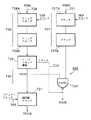
【0056】
具体的には、図8を参照して説明すると、BNCコネクタ302(トランシーバー171を介して)と、RJ−45コネクタ301は、それぞれネットワーク制御部510のセレクタ511につながれている。ネットワークトラフィックは、セレクタ511の状態に応じて、バス181及びBNCコネクタ302又はRJ−45コネクタ301を介して、マイクロプロセッサー173に入出力される。セレクタ511の位置は、制御レジスタ521の出力によって判断される。
【0057】
RJ−45コネクタ301がLANに接続すると、電流がコネクターに供給される。従って、ネットワーク制御部510は、RJ−45コネクタ301が電気的にLAN100に接続されていることをRJ−45コネクタ301が判断するところを監視する、リンク良好検出部512を含む。83902ネットワーク制御部においては、リンク良好検出部512は、開放ドレイン型(open drain)のN−チャンネルデバイスとして構成されている。電流がRJ−45コネクタ301で検出されると、リンク良好検出部512からの出力は低くなり、状態LED305が点灯することにより、電気的に接続していることを示す。反対に、RJ−45コネクタ301に電流がない場合、リンク良好検出部512からの出力は高くなり、状態LED305は消灯する。リンク良好ビットは、NEB制御論理回路520のリンク良好レジスタ522にも入力される。これにより、マイクロプロセッサー173はリンク良好信号の状態を読み込めるようになる。
【0058】
BNCコネクタ302などのBNCコネクタは、例えば、LANにT−タイプの同軸アダプタを用いてつながれたときなど、コネクタが適切に終端するまでジャバーし続ける。ネットワーク制御部510は、当業者に知られる方法でBNCコネクタ302でジャバリングがあるかどうかを検出するジャバー検出回路513を含み、その検出結果をジャバーレジスター514に書き込む。従って、ジャバーレジスタ514は、BNCコネクタ302が適切に終了したか否かを示すビットを含む。そして、このジャバービットはソフトウエアによって読み込まれる。
【0059】
マイクロプロセッサー173は、フラッシュEPROM174に格納されているソフトウエアモジュールを実行することによって、セレクタ511の状態を制御する。制御の方法は、以下に図9のフローチャートを参照にして説明する。NEB101が投入された後(ステップS900)、マイクロプロセッサー173は、0を制御レジスタ521にバス181を介して書き込むことにより、セレクタ511をRJ−45の位置へ設定する(ステップS901)。プログラムはリンク良好レジスタ522の状態を読み込み(ステップS902)、そして、リンク良好レジスタ522に記憶されたビットが低レベルならば(電流を示唆する)、プログラムはRJ−45コネクタ301がLAN100に接続され、処理を抜けて、セレクタ511をRJ−45の位置に残しておく(ステップS903、S904)。
【0060】
リンク良好検出部512を構成するN−チャンネルデバイスのスイッチングにおいて、固有の遅れがあるために、電気的接続を検出するための充分な時間をリンク良好検出部512に与えることが必要である。従って、リンク良好レジスタ522に記憶されているビットが高レベルならば(電気的接続がないことを示す)、プログラムはリンク良好レジスタ522を繰り返し読み込み、読み出した内のどれかが低レベルならば、処理を抜けて、セレクタをRJ−45の位置に留めておく(ステップS905−S906−S902)。しかし、読み込みを500回繰り返してもリンク良好レジスタ522に記憶されているビットが高レベルである場合は、プログラムは1を制御レジスタ521へ書き込むことによって、セレクタ511をBNCの側に設定する(ステップS907)。
【0061】
そして、プログラムはジャバーレジスタ514を読み込む(ステップS908)。ジャバーレジスタ514の状態が低レベルならば(BNCコネクタ302が適切に終端し、BNC接続があることを示す)、プログラムは処理を抜けて、セレクタ511をBNCの側に残しておく(ステップS909及びS910)。ジャバービットの状態が高レベルの場合(BNCコネクタ302が不適切に終端し、LAN100に接続されていないことを示す)、プログラムはステップS901へ戻り、セレクタ511をRJ−45の位置へリセットする。そして、RJ−45又はBNC接続が設定されるまで、プログラムは定期的に再実行される。
【0062】
このように、NEB101はBNCコネクタ302とRJ−45コネクタ301の間を断続し続け、特定のコネクタがLAN100に接続されたことをトグルする度に確認する。この構成により、電源投入時(及び接続がなされるまで)に、NEB101は、操作者が実際にスイッチを変えることを必要とせずに、そのBNCコネクタ302又はRJ−45コネクタ301がネットワークに接続されたか否かを判断することができる。従って、NEB101が、LAN100につながれていないコネクタを通してLAN100と通信しようとする可能性がなくなる。
【0063】
本実施の形態において、電力が供給されている現サイクル中、選択されたハードウエア接続は保持される。電力が供給されている現サイクル中において選択がなされた後に、ハードウエア接続が有効でなくなったときを感知し、選択処理を繰り返し、コネクタを変更することを許可するソフトウエアを実行することは可能である。これにより、一つの接続から他の接続へのダイナミックな切り換えを可能にする。
[ネットワークプロトコルセンサー]
マルチプロトコルシステムにおける適切な操作を確実にし、またネットワーク上で使用されるプロトコル及びフレームタイプに関する不適切な前提を作らせないようにするために、NEB101は、ネットワークトラフィックで使用されるフレームタイプを決定し、NEB101が使用することのできる数種の異なるプロトコルのうちのある一つにこれらのフレームタイプを関連させるための自動プロトコル判断を使用する。特に、フラッシュEPROM174に格納されているPRETASKモジュールの使用を通じて、NEBマイクロプロセッサー173は、どのフレームタイプがネットワークトラフィックのために使用されているかを判断し、そのフレームタイプを数種の異なるプロトコルの一つに関連づけ、そのプロトコル及び検出されたフレームタイプを使用したネットワーク通信を続けるために、フラッシュEPROM174からプロトコルスタック(IPX/SPX又はTCP/IP等)をロードすることができる。
【0064】
図10乃至図14は、この処理を説明する為の図である。図10は、フラッシュEPROM174にロードされたPRETASKソフトウエアモジュールに基づいて、NEBマイクロプロセッサー173によって実行される処理ステップを示すフローチャートである。PRETASKは、異なってはいるが、PRESCANソフトウエアモジュールに似ている。PRESCANソフトウエアモジュールは、審査中の特許出願番号第07/978,409の、「ローカルエリアネットワーク上で扱われるデータパケットの形式を適応判断する方法及び装置(Method And Apparatus For Adaptively Determining The Format Of Data Packets Carried On A Local Area Network)」に示されている通りである。
【0065】
ステップS1001で、マイクロプロセッサー173はMLID(マルチリンクインターフェースドライバ)をフラッシュEPROM174からDRAM175へロードし、MLIDを実行開始する。上記のとおり、MLIDはネットワークと通信する、最下層ソフトウエアである。したがって、MLIDはネットワーク線上で扱われるネットワークフレームパケットへの直接のソフトウエアインターフェースとして振る舞う。
【0066】
ステップS1002において、マイクロプロセッサー173はMLIDの上層にLSL(リンク補助層)をロードし、LSLを実行開始する。LSLは、下層のMLIDとその上層にロードされる様々なプロトコルスタックとの間の、マルチプレクサとして機能する。特に、LSLは、ネットワーク上でフレームパケットを運ぶ、様々なフレームタイプの登録を受け入れる。従って、例えばEthernet環境では、LSLは802.2、802.3、Ethernet_II、Ethernet_Snap等の登録を受け入れ、またToken-ring環境では、LSLは802.5、及びToken_Ring_Snapの登録を受け入れる。フレームタイプをLSLに登録することにより、LSLより上層のソフトウエアモジュールは登録されたフレームタイプに適合する全てのフレームパケットをモジュールに供給するように、LSLに命令する。
【0067】
ステップS1003において、マイクロプロセッサー173はLSLより上層にPRETASKをロードする。上記のとおり、PRETASKは、NEB101が通信を受け入れられた様々なプロトコルに、どのフレームタイプが関連するかを識別する。ステップS1004で、LSLから受信するために、PRETASKはMLIDにサポートされた全てのフレームタイプを登録する。従って、本実施の形態におけるEthernet環境では、PRETASKは802.2、802.3、Ethernet_II、Ethernet_SnapをLSLに登録し、これにより、登録されたフレームパケットに適合する全てのフレームパケットをPRETASKに供給するように、LSLに命令する。
【0068】
処理はステップS1005へ進み、MLIDとLSLはネットワークのトラフィックを監視する。特に、ステップS1005では、ネットワークはブロードキャストトラフィック手段を監視して、トラフィックの行き先が決定されていない(つまり、行き先はどこでもよい)ことを観察する。通常、ブロードキャストトラフィックは、行き先のMACアドレス、例えば16進法のFが12並んでいるアドレスなどのグローバルな特定によって識別される。LANブロードキャストトラフィックが検出されるまでは、PRETASKは何もしない。
【0069】
PRETASKを実行中のこの時点では、様々なソフトウエアモジュールの関係は図11に示すとおりである。図から分かるように、それぞれが異なるフレームタイプを用いる異なるプロトコルを起動している機器182、183、184、及び185などの複数のネットワーク機器全てが、一つのLAN100に接続する可能性がある。図11において、機器182はNovelタイプの機器で802.2フレームタイプを使用するIPX/SPXプロトコルを起動しており、機器183はUNIXタイプのネットワーク機器でEthernet_IIフレームタイプを使用するTCP/IPプロトコルを起動しており、機器184はMacintoshタイプの機器でEthernet_Snapフレームタイプを使用するEtherTalkプロトコルを起動しており、機器185は不明のフレームで、802.3フレームタイプを使用するプロトコル機器である。言うまでもなく、図11に示す組み合わせは図示のためだけのものであり、これに限られるものではなく、例えば、NovellのIPX/SPXが802.3フレームタイプ又は他のフレームタイプを使用することも可能である。ただし、それぞれのプロトコルが唯一のフレームタイプにのみ、関連づけられなければならない。
【0070】
NEB101はまたLAN100に接続されており、MLID186の上層にロードされたLSL187を含む。PRETASK188は、LAN100上にブロードキャストされる異なるフレームタイプをそれぞれ登録したものとして示されている。従って、図11に示すように、PRETASK188は、802.2を189に、Ethernet_IIを190に、Ethernet_Snapを191に、そして802.3を192に登録している。
【0071】
LANブロードキャストトラフィックが検出されると、ステップS1006へ進み、LSLはPRETASKへフレームパケットを供給する。ステップS1007で、そのフレームパケットで使用されているプロトコルを識別するために、PRETASKはフレームのプロトコルのヘッダを復号する。このヘッダへのオフセットは、プロトコルが使用しているフレームタイプによって異なる。下記のテーブルは16進法による値と、異なるプロトコルを識別するためのプロトコルのヘッダの数例を含む。
【0072】
図10のステップS1008において、PRETASKは、LSLから受信したばかりのフレームタイプの登録を取り消す。従って、図12の189aに示すとおり、PRETASKは802.2の登録を取り消す。
ステップS1008では、全ての場合に登録を取り消す場合を示しているが、登録を取り消さないほうがより好ましい場合もある。特に、それぞれ異なるプロトコルがそれに関して、受け入れ可能なフレームタイプのリストを持つ場合である。IPX/SPX及びTCP/ITの受け入れ可能なフレームタイプの例を以下に示す。
【0073】
ステップS1009において、PRETASKは、ステップS1007で復号したプロトコルに対応するプロトコルスタックをロードする。図12の例では、IPX/SPXプロトコルが復号されたので、PRETASKはフラッシュEPROM174からIPX/SPXプロトコルスタックをロードする。ロードする前に、プロトコルスタックは、LSLから受信したばかりのフレームタイプ、ここでは802.2で初期化される。
【0074】
ステップS1010では、新たにロードされたプロトコルスタックは、例えば図13に示すように、LSLに登録される。図に示すように、IPX/SPXプロトコルスタックは802.2をLSLに登録する。上記のように登録することによって、登録されたフレームタイプ(ここでは802.2)に適合する全てのフレームパケットを新たにロードされたプロトコルスタックに提供するように、IPX/SPXは、LSLに通知する。
【0075】
そして、ブロードキャストトラフィックのために引き続きネットワークを観察するために、PRETASKはステップS1005へ戻る。LSLが、PRETASKによって登録された残りのフレームタイプに適合するフレームパケットを見つけると、LSLは、図10に示す処理を行うためにこれらのフレームタイプをPRETASKに供給する。このように、例えばTCP/IPプロトコルに関連するフレームタイプのような追加フレームタイプが見つかる度に、フラッシュEPROM174から適切なプロトコルスタックがロードされるように、これらのフレームはPRETASKによって処理される。
【0076】
また、図14に示すように、プロトコルスタックは既にロードされているため、ネットワーク上での操作を開始する。特に、PRETASKが完全に受け身で、ネットワーク通信をブロードキャストしないのに対し、IPX/SPXはそれに関するSAPリクエストをブロードキャストする。PRETASKによってロードされた他のプロトコルタスクは、それらに関連するリクエストをブロードキャストしてもよい。例えば、TCP/IPプロトコルスタックがロードされた場合、最も近くのネットワークサーバーからそのアドレスを得るために、RARPSをブロードキャストする。
[スマートフラッシュ]
ローカルエリアネットワークがより複雑になるにつれて、NEB101のようなネットワークインターフェースカードを、最新の技術を用いてグレードアップする必要性が出てきた。従って、NEB101は操作用ソフトウエアに組み込まれているため、そのソフトウエアを後でLAN100から再プログラムすることができる。例えば、ネットワーク統括者は、統括者のPC103から新しいデータをダウンロードすることによって、フラッシュEPROM174のROMファームウエアイメージデータを遠隔操作で変更することができる。その新しいデータは、例えば、パッチコードと、製造テストルーチンと、ファームウエア全体の更新と、異なる言語バージョンとを含む。
【0077】
典型的なPCは、2つ以上のLANに接続されている。例えば、図15に示すように、PC103はEthernetのLANであるLAN100と、Token-ringLANであるLAN193とに接続しており、実際に両ネットワークのネットワーク統括者用PCとして機能してもよい。それぞれのLANはまた、独立したNEBをそれぞれ内蔵する複数のプリンターに接続されていてもよい。また、他の再プログラム可能な機器を、これらのLANの一方又は両方に接続することもできる。従って、ネットワーク統括者が潜在的に再プログラムすることができる、複数のNEBや他の機器がある。
【0078】
ある特定のNEBを再プログラムする場合、ネットワーク統括者はPC103から、ネットワークに接続されている全てのネットワーク機器から適切なフラッシュターゲットを識別するために、そのネットワークのバインダリーをスキャンするためのプログラムを稼働する。適するフラッシュターゲットは、フラッシュ機能を持ち、Ethernet機器及びToken-ring機器を含む、NEBのような機器を全て含む。ネットワーク統括者は、再プログラムのために機器の一つを選択し、その機器とのネットワーク通信を確立する。そしてボード上のフラッシュEPROMは、新しいイメージデータでそれ自身を再プログラムする。
【0079】
ネットワーク統括者が、ネットワークに接続されたいくつかの再プログラム可能ボードをそれぞれ含む、2つ以上のネットワークを統括している場合があるため、統括者は適切なイメージデータが目的のNEBに送られたことを確認しなければならない。従って、ネットワーク統括者が、NEB101上のフラッシュEPROM174を再プログラムしたい場合(NEBはEthernet LANに接続されている)、送信するイメージデータがEthernetイメージデータであることを確認し、NEB101の他の機能と互換性があることを確認しなければならない。
互換性がないイメージデータをダウンロードした結果は、破壊的なものでありうる。例えば、ネットワーク統括者が誤ってToken-ringイメージデータをNEB101にダウンロードし、その後にNEB101がフラッシュEPROM174をそのイメージデータで再プログラムした場合、フラッシュEPROM174はEthernet LAN100上で通信を行うことが全くできなくなる。これはつまり、NEB101がLAN100から再プログラムすることさえできないことを意味する。Ethernet LANに関しては全く「役立たず」のボードとなるわけである。例えば、ホストインターフェース構成(NEBとそれが内蔵されている周辺機器間のインターフェースのタイプ)や、製品構成(NEBのボードのタイプ)や、プロセッサー構成(ボード上のプロセッサーのタイプ及び速度)や、メモリ構成(ボードメモリ上の様々な部品のサイズ及び消去性)における非互換性は、問題となる可能性がある。従って、ある製品の前世代のものがある場合、新しい世代のものでしか動かないフラッシングソフトウエアはやはり「役立たず」のボードとなってしまうのである。
【0080】
互換性のないイメージデータがダウンロードされた場合にこのような悲惨な結果を招かないようにするために、NEB101は、実際に再プログラムが行われる前に、ダウンロードされたイメージデータが互換性のあるものであるかを確認するソフトウエアコードを含む。具体的には、NEB101のフラッシュEPROM174は、NEB101のための構成情報を含むネットワーク情報ファイル(NIF)ブロックを含む、現プログラムイメージデータと、フラッシュEPROM174を再プログラムするためのソフトウエアモジュールとを記憶する。マイクロプロセッサー173はネットワーク通信を送受信し、そして新しいプログラムイメージデータをネットワークから受信した時に、マイクロプロセッサー173はその新しいプログラムイメージデータをDRAM175へダウンロードし、その新しいプログラムイメージデータがNIFブロック中の構成情報と互換性があることを確認し、そして、互換性が確認された場合に限ってフラッシュEPROM174を再プログラムする。
【0081】
更に詳しくは、NIFブロックは、恒常的なアダプタ特有の構成情報を含み、それぞれの個別のNEBに特有のものである。一例としては、NIFブロックはフラッシュEPROM413中のメモリスペースのうち32バイトを占め、それぞれ8バイトの4バンクに分けられる。図16に示すように、NIFブロックは、MACアドレス情報バンクと、ボードバージョン及び識別情報バンクと、構成要素識別情報バンクと、一般情報バンクとを含む。
【0082】
MACアドレス情報バンクは、その名が示すとおり、ボードに特有のMACアドレスを記憶する。ボードバージョン及び識別情報バンクは、4つのバンクに更に分割される。NEB以外のネットワークインターフェースカードをLANにつなぐことも可能なため、製品カテゴリーバンクはLANにつながれた製品のタイプを識別し、そしてボード修正バンクは製品の修正番号を識別する。
【0083】
ネットワーク物理的媒体バンクは更に2つのバンクに分割される。これらは、ボードが使用されている物理的媒体(例えば、Ethernet、Token-ring、FDDIなど)を識別する物理的ネットワークバンクと、ボードが補助する物理的コネクタ(例えば、Ethernetネットワークの場合は10baseTと、10base2と、10base5、そしてToken-ringの場合はUTP及びSTP)のタイプを識別する補助接続バンクである。ホストインターフェース方法バンクでは、ボードを内蔵する周辺機器(NEB101の場合は、プリンター102等)へのインターフェースのタイプを識別する。これらのインターフェースタイプの例としては、共用RAMや、小型コンピューターシステムインターフェース(SCSI)や、標準パラレルインターフェースや、RS−232Cシリアルインターフェースや、セントロニクスパラレルインターフェース等がある。
【0084】
構成要素識別情報バンクもまた、いくつかの更に小さいバンクに分けられている。これらのバンクは、ボード上のROMや、DRAM及びNVRAMのサイズ及び細かさと、ROMの消去性を識別する。また、ネットワーク制御部(Ethernetの場合はDP83902チップ、Token-ringの場合はTI389C25)及びホスト制御部(調停された共用RAM、NCR53C90A SCSIコントローラー又はNCR53C80 SCSIコントローラー)が識別される。CPU識別バンクには、プロセッサーのタイプとクロックスピードが記憶される。最後に、一般情報バンクは、ハードウエア修正レベル等、ボードに関する追加構成属性を識別するための他のデータを記憶する。
【0085】
次に図17のフローチャートを参照して説明する。ネットワーク統括者のPC上のCPFLASHプログラムがバインダリーをスキャンしたときに、NEB101のフラッシュEPROM174の再プログラミングが開始され(ステップS1401)、潜在的なフラッシュターゲットのリストを統括者に表示する。統括者はターゲットを選択し(ステップS1402)、CPFLASHはそのターゲットとの通信を確立して、新しいフレームウエアイメージデータをLANへダウンロードし、NEBのDRAM175に記憶する(ステップS1403)。
【0086】
一度新しいイメージデータがDRAM175にダウンロードされると、現在実行されているプロトコルスタックはプログラムされようと(少なくとも潜在的に)しているので、プログラムされている間はネットワーク通信を行うことができないので、NEBマイクロプロセッサー173は、そのプロトコルスタックをインアクティブにする(ステップS1404)。マイクロプロセッサー173は次に、現在のNIFブロックをフラッシュEPROM174からDRAM175にコピーし(ステップS1405)、ソフトウエア再プログラミングモジュールを実行する。
【0087】
そして、ソフトウエア再プログラミングモジュールは、新しいイメージデータが互換性があることを確認するために、現イメージデータNIFブロックに記憶されている情報(DRAM175にコピーされた情報)を参照して、その情報を新しいフレームウエアイメージNIFブロックに記憶されている情報と比較して、イメージデータが互換性チェックを行う(ステップS1406)。NIFブロックはNEB101に関する多量の情報を持っているため、様々なチェックを行うことによってこのような互換性を判断することができる。
【0088】
最初の互換性チェックは、NIFブロックの物理的ネットワークバンクに記憶されたデータを参照することによって行う、新しいイメージデータが正しいネットワーク媒体のタイプか否かを判断するためのネットワーク媒体構成チェックを含む。同様に、2番目の互換性チェックは、NIFブロックのホストインターフェース方法バンクとホストインターフェース制御部バンクに記憶されたデータと新しいイメージデータとを比較することによって行う、新しいイメージデータが適切なホスト(例えば、共有RAM又はSCSI)にインターフェースするためのイメージデータであるか否かを判断するためのホストインターフェース構成チェックを含む。
【0089】
3番目の互換性チェックは、NIFブロックの製品カテゴリーバンクとボード修正バンクを参照し、そのデータを新しいイメージデータと比較することによって行われる、新しいイメージデータがEPROMが内蔵されたボードのタイプの為のものであるか否かを判断するための製品構成チェックを含む。また、プロセッサー構成チェックは、新しいイメージデータがボード上のプロセッサーと互換性があるか否かを判断するために、NIFブロックのCPUバンクを参照することによって行なうことができる。更に、メモリ構成チェックは、新しいイメージデータがボードのメモリと互換性があるか否かを判断するために、NIFブロックのROMバンク、DRAMバンク、及び/又はNVRAMバンクに記憶されているデータを新しいイメージデータと比較することによって行なうことができる。NIFブロックに記憶された他の情報を使用することによって、他の互換性チェックを行うこともできる。
【0090】
新しいイメージデータが互換性が無いと判断された場合、現プロトコルスタックは再度アクティブにされ(ステップS1407、S1408)、LAN100を通して、ネットワーク統括者のPC103にエラーを告げ、互換性が無いイメージデータを用いてNEB101を再プログラムする試みがなされたことを知らせる(ステップS1409)。
【0091】
反対に、新しいイメージデータが互換性がある場合、ボード特有の情報(MACアドレスやボード修正番号等)を保持するために、新しいイメージデータのNIFブロックのボード不変部分が、現イメージデータのNIFブロックの対応する部分で置き換えられる(ステップS1407とS1410)。そしてプログラムは現イメージデータをフラッシュEPROM174から消去し、上記の処理によってオリジナルのNIFブロックを含んでいる、DRAM175に記憶された新しいイメージデータでフラッシュEPROM174を再プログラムする。
【0092】
この構成により、互換性の無いイメージデータが誤ってLAN100からダウンロードされた場合でも、マイクロプロセッサー173が、互換性の無いイメージデータでフラッシュEPROM174を再プログラムすることがなくなる。そればかりか、ネットワーク統括者が互換性の無いイメージデータでNEB101を再プログラムしようとした場合、NEB101は、互換性の無いことを知らせるメッセージをネットワーク統括者に送る。従って、このような人的なエラーに対応する、失敗することのないメジャーが、安価で効率的な方法で供給される。
[アービトレーション機器]
図18乃至図20は、プリンターインターフェースカード150又はボード上のNEBマイクロプロセッサー173からのアクセスリクエストに応答した、共有SRAM200のアービトレーションを説明する図である。
【0093】
図18は、プリンターアドレス/データバス(A/Dバス)701と、印刷アドレスラッチイネーブル(ALE)信号702と、プリンターデータイネーブル(DEN)信号704と、プリンタークロック線705と、プリンター準備完了信号706とを示す。これらの信号は全て、プリンターインターフェースコネクタ170を介して、プリンターインターフェースカード150から受信される。具体的には、例えば、A/Dバス701は、プリンターインターフェースカード150に搭載されたプリンターマイクロプロセッサー151の為のA/Dバスである。プリンターALE信号702は、有効なアドレス情報がA/Dバス701上で運ばれた時を示す信号であり、そして、プリンターDEN信号704は、有効データ情報がA/Dバス701上で運ばれた時を示す信号である。プリンタークロック705はプリンターマイクロプロセッサー151の為の主要クロック信号で、プリンター準備完了信号706は、それが「偽」である場合に、メモリアクセスが完了していないことと、メモリアクセスが完了するまで続けるように、マイクロプロセッサー151が待機状態を挿入しなければならないことを示す信号である。
【0094】
また、図15には、NEBアドレス/データバス(A/Dバス)711と、NEB ALE信号712と、読み込み及び書き込み信号(WR及びRD)714と、NEBクロック715と、NEB準備完了信号716とが示されている。NEB A/Dバス711は、マイクロプロセッサー173のための主要アドレスバスであり、NEB101に搭載された全ての構成要素のアドレス及びデータ情報を運ぶ。NEB ALE信号712は、有効なアドレス情報がA/Dバス711上に現われた時を示す信号であり、読み込み及び書き込み信号714は有効データ情報がA/Dバス711上に現われた時を示し、さらに、そのデータを読み込むか書き込むかを示す信号であり、NEBクロック715は水晶発振機172によって供給される主要クロック信号であり、NEB準備完了信号716は、それが「偽」である場合に、メモリアクセスがまだ行うことができないことと、メモリアクセスを行えるようになるまでマイクロプロセッサー173が待機状態を挿入するように、NEBマイクロプロセッサー173に知らせる信号である。
【0095】
上記のとおり、プリンターマイクロプロセッサー151とNEBマイクロプロセッサー173は、共有SRAM200を介して通信する。共有SRAM200へのアクセスリクエストは、プリンターマイクロプロセッサー151とNEBマイクロプロセッサー173によって、A/Dバス701及び711上にそれぞれ発行される。そして上記のとおり、アービター制御論理回路400によって調停される。更に詳しくは、図6を参照して説明したとおり、アービター制御論理回路400は、NEB A/Dバス711上のバスアクセスを制御するためのバス制御論理回路410と、プリンターA/Dバス701上のバストラフィックを制御するためのバス制御論理回路420と、A/Dバス701およびA/Dバス711上のアクセスリクエストの調停を行うための共有メモリアービター430と、プリンターA/Dバス701とNEB A/Dバス711を、それぞれSRAMのためのアドレス及びデータバスにインターフェースするためのSRAMインターフェース440とを含む。これらの部分のそれぞれは、以下に詳しく説明する。
【0096】
バス制御論理回路410は、ラッチされたアドレス情報719を提供するために、NEB ALE信号712に応答してNEB A/Dバス711上のアドレス情報をラッチする、ラッチ717を含む。復号部720は、読み込み及び書き込み信号714がアクティブであるときに、NEB A/Dバス上のアドレス情報が共有SRAM200のアドレス空間に対応している場合に、NEBリクエスト信号(NREQ信号)721を提供するために、ラッチされたアドレス情報を復号する。
【0097】
同様に、バス制御論理回路420は、プリンターALE信号702が高レベルであるときに、ラッチされたアドレス情報724を提供するために、プリンター A/Dバス701上のアドレス情報をラッチするラッチ722を含む。復号部725は、プリンターDEN信号704がアクティブであって、ラッチされたアドレス情報が共有SRAM200のアドレス空間に対応している場合に、ラッチされたアドレス情報に応答し、プリンターリクエスト信号(PREQ)726を出力する。
【0098】
共有メモリアービター430は、PREQアクセスリクエスト信号とNREQアクセスリクエスト信号を共通のクロック(ここではNEBクロック715)に同期させるための同期回路と、上記リクエスト信号のどちらかに断片的なクロックディレイを鋏み込む遅延回路と、最初に受信したリクエスト信号にアクセスを許可し、後で受信されたアクセスリクエストを延期する延期回路と、再同期回路とを含む。特に、NREQ721とPREQ726は共に、共通のクロックに同期させるためにNEBクロック715に同期させる同期回路に入力する。ここで示す一例では、プリンタークロック信号705に固有に同期されたPREQは、NEBクロック信号715に同期される。遅延信号729は、オフセットリクエスト信号を生成するために、アクセスリクエスト信号のどちらか一方(ここではプリンターからのアクセスリクエスト信号)に挿入される。遅延回路は、2つのアクセスリクエストが共に全く同時に発行された場合でも、一方のアクセスリクエストが延期回路730に他より必ず先に到着するように、2分の1クロック遅延の様な、断片的なクロック遅延信号を挿入する。
【0099】
延期回路730は、第1及び第2のアクセスリクエスト信号に応じて、第1及び第2アクセス許可信号、PACK及びNACKを出力する。第1及び第2オフセットリクエスト信号で先に受信された順番に応じて、第1及び第2アクセス許可信号の厳密に一方がアクティブにされる。他の(つまり、後で受信された)オフセットリクエスト信号は、先に受信されたアクセスリクエスト信号の処理が終了するまで延期される。延期されたマイクロプロセッサーにアクセスが拒否されたことを示すために、準備未完了信号が発行される。例えば、NEBアクセスリクエストが、プリンターアクセスリクエストより後に受信された場合、延期回路730はプリンターにアクセス許可を与え、NEBからのアクセスを延期する。この場合、NEB準備完了信号716は取り下げられ、アクセス許可がおりるまで待機状態を挿入するように、マイクロプロセッサー173に示す。反対に、NEBアクセスリクエストが、プリンターアクセスリクエストより先に受信された場合、延期回路730はNEBにアクセス許可を与え、プリンターのアクセスを延期する。この場合、延期回路730はプリンター準備完了信号を遅らし、マイクロプロセッサー151にアクセス許可がおりるまで待機状態を挿入するように指示する。
【0100】
プリンターのためのPACKアクセス許可信号は、同期しないように制御された信号をそれ自身のクロックに再同期するように、再同期回路731へ入力される。この再同期された信号はFPACKとして指示される。再同期されたアクセス許可信号FPACK及びNACKは、アクセス許可を受けたマイクロプロセッサーと共用SRAM200との間の適切なインターフェースを提供する、SRAMインターフェース440に入力される。
【0101】
共用メモリアービター430は、Dタイプフリップフロップ及び標準の論理回路で構成することが好ましい。好ましい構成の一つを図19に示す。図19に示されるように、プリンターからのアクセスリクエスト信号726は、NEBクロック信号715にクロックされる、同期するDタイプフリップフロップ728aに入力され、その後、第2のDタイプフリップフロップ728bに入力する。同時に、NEBからのアクセスリクエスト信号721は、Dタイプフリップフロップ727aに入力され、その後、第2のDタイプフリップフロップ727bに入力する。これら2つのフリップフロップ727a及びフリップフロップ727bは、アクセスリクエスト信号721に適した同期及び遅延を確認するために提供される。立下がり制動Dタイプフリップフロップ729は、プリンターからのアクセスリクエスト信号726に、1.5クロックの遅延を挿入するために供給されている。フリップフロップ729の出力は、アクセス許可信号がNEBに既に供給されている場合(つまり、NACK信号が高レベル)に供給されるリセット信号732によって、低レベルに保たれる。反対に、NEBに対してアクセス許可が下りていない場合、プリンターからのアクセスリクエスト信号は、PACK信号を形成するために、クロックスルー(clocked through)される。このPACK信号は、プリンタークロック705によってクロックされる再同期フリップフロップ731へ送られる。同時に、PACK信号は、クロックされたNEBアクセスリクエスト信号に連動するNANDゲート734に供給される。プリンターにアクセス許可が下りると、NANDゲート734は、アクセスリクエストがあったとしても、PACKが低レベルに変わるまで、NEBのアクセスが拒絶されたことを確認する。
【0102】
図19に示す構成により、延期回路730が第1及び第2の許可信号を出力したとしても、一時に、これら2つの許可信号のうちのどちらか一方のみがアクティブにされる。つまり、プリンターにアクセス許可が下りると、NEBのアクセスは延期される。逆に、NEBにアクセス許可が下りると、プリンターのアクセスは延期される。
【0103】
図18に戻ると、SRAMインターフェース440は再同期されたプリンターアクセス許可信号FPACKと、NEBアクセス許可信号NACKとを受信し、この信号のうちどちらがアクティブにされているかに基づいて、プリンターマイクロプロセッサー151とNEBマイクロプロセッサー173の間での、共有SRAM200へのアクセスを調整する。
【0104】
更に詳しくは、図18に示すとおり、NEBアクセス許可信号NACKはマルチプレクサ735へ供給される。このマルチプレクサ735は、ラッチされたNEBアドレス情報719又はラッチされたプリンターアドレス情報724のどちらかを、NACK信号に基づいて選択し、選択されたアドレス情報を内部アドレスバス736へ供給する。NACKがアクティブである場合、マルチプレクサ735は、ラッチされたNEBアドレス情報719の13ビット全てを、内部アドレスバス736へ供給する。反対に、NACKがアクティブでない場合(つまり、プリンターがアクセス権を持つ)、マルチプレクサ735は、ラッチされたプリンターアドレス情報724の13ビットの内、12ビットを内部アドレスバス736へ供給する。第13番目のビット、ここではAOは、ジェネレーター747によって、以下に示す方法で供給される。
【0105】
バッファ737は、内部アドレスバス736からのアドレス情報をSRAMアドレスバス740にバッファする。バッファ737はORゲート739の出力により、アクティブにされる。ORゲート739は、NEBアクセス許可信号NACKを入力の一つとして受け付ける。これにより、NACKが高レベルになるとすぐに、バッファ737は、内部アドレスバス736上のアドレス情報をSRAMアドレスバス740にバッファする。
【0106】
読み込み又は書き込みのどちらがリクエストされたかによって、つまり、読み込み又は書き込み信号714の状態に応じて、SRAM200はデータ情報を、データバス741から受信またはデータバス741へ送出する。このデータ情報は、両方向バッファ742を介して内部データバス744へ送信される。両方向バッファ742は、NEBアクセス許可信号NACKを入力の一つとして受け付ける、ORゲート745からの出力によってアクティブにされる。従って、NACKが高レベルになると、ORゲート745の出力も高レベルになり、SRAMデータバス741から内部データバス744へのデータ情報の送信を許可することになる。内部データバス744上のデータ情報は、NEBアクセス許可信号NACKによってアクティブにされる両方向バッファ746を介して、NEB A/Dバス711へ送出される。NEBアクセス許可信号NACKは、読み込み又は書き込み信号714によって起動される復号部720から最終的に導き出されるため、バス711が有効なアドレスデータが出現することを期待せず、有効なデータ情報が出現することを期待するので、NEB A/Dバス711上のデータ情報のタイミングは適切である。
【0107】
従って、まとめると、NEBが共有SRAM200にアクセスする許可を受けると、ラッチ717からのラッチされたアドレス情報は、マルチプレクサ735及びバッファ737を介して、SRAMアドレスバス740にバッファされ、データ情報は、両方向バッファ742及び746を介して、NEB A/Dバス711へ(から)SRAMデータバス741から(へ)バッファされる。NEBのためのアクセス操作が終了すると、プリンターからの延期されたアクセスリクエストが処理される。
【0108】
プリンターマイクロプロセッサー151が、共有SRAM200にアクセスする許可を受けている場合には、NEBマイクロプロセッサー173が使用するのと同じ13ビット幅のアドレスを、プリンターマイクロプロセッサー151が使用していたとしても、プリンターマイクロプロセッサー151はSRAM200のデータバス幅と異なるものを持っているため、これらのビット幅の差を解決するために、上位又は下位バイトバッファが必要とされる。詳しくは、上記のとおり、プリンターマイクロプロセッサー151は、規則に基づいて16ビット幅の共有RAMデータアクセスを通して外部機器と通信する、32ビットのインテル80960KBRISCマイクロプロセッサーである。プリンターマイクロプロセッサー151の内部32ビットフォーマットへの16ビットアクセスの問題解決は、プリンターマイクロプロセッサーに依存する。しかし、8ビット幅の共有SRAM200への、プリンターマイクロプロセッサー151からの16ビットデータアクセスの問題解決は、SRAMインターフェース440及び上記の上位又は下位バイトバッファに依存する。この構造を以下に更に詳しく説明する。
【0109】
具体的には、ラッチ722でラッチされたアドレス情報については、マルチプレクサ735は13ビット中の12ビットを、内部アドレスバス736へ送信する。第13番目のビット、ここではAOは、ジェネレーター747から供給される。ジェネレーター747は、ストローブ(strobe)ジェネレーター751からの下位ストローブ出力750及び上位ストローブ出力752によってアクティブにされる。ストローブジェネレーター751は、共有メモリアービター430からのFPACKアクセス許可信号の受信に応じて、2つの連続する信号、つまり下位ストローブ750及び上位ストローブ752を供給するように構成されている。下位ストローブ信号750はジェネレーター747へ供給され、ジェネレーター747は二値の0ビットを第13番目のアドレスビットのために、マルチプレクサ735へ供給する。マルチプレクサ735は、これらの13のアドレスビットを選択し、内部アドレスバス736へ出力する。内部アドレスバス736に関するアドレス情報は、上述したとおり、バッファ737を介してSRAMアドレスバス740へラッチされる。バッファ737は下位ストローブ750及び上位ストローブ752をその入力として含む、ORゲート739の出力によってアクティブにされる。従って、続く下位ストローブ750及び上位ストローブ752に応じて、ORゲート739はバッファ737へ信号を出力し、これにより、内部アドレスバス736上のアドレス情報が、SRAMアドレスバス740へ送信されることになる。
【0110】
上位アドレスストローブ752は、ジェネレーター747へも供給され、ジェネレーター747は二値の1を第13番目のアドレスビットとして生成し、マルチプレクサ735へ供給する。マルチプレクサ735は、内部アドレスバス736へ出力する、これらの13ビットを選択する。ORゲート739による上位ストローブ752の受信に続いて、この更新されたアドレス情報は、SRAM200のアドレスバス740へ送出される。
【0111】
データ情報の取り扱いは、プリンターマイクロプロセッサー151によって読み込み、書き込みのどちらがリクエストされたかによって変わる。書き込みの場合、ストローブジェネレーター751は、バッファ754へ下位ストローブ信号750を供給する。バッファ754はプリンターA/Dバス701に関するデータ情報の下位バイトを内部データバス744にバッファする。そしてプリンターアクセス許可信号FPACKをその入力の一つとして受け入れるORゲート745の出力によってアクティブにされる両方向バッファ742を介して、このデータ情報はSRAMデータバス741にバッファされる。従って、プリンターA/Dバス701上にあるデータ情報の下位バイトはバッファ754を介して、内部データバス744、それからSRAMデータバス741にバッファされる。
【0112】
プリンターA/Dバス701上にあるデータ情報の上位バイトは、ストローブジェネレーター751からの上位ストローブ752によってアクティブにされるバッファ755によってバッファされる。上記と同様に、データ情報の上位バイトは両方向バッファ742を介して、内部データバス744、それからSRAMデータバス741に送信される。
【0113】
プリンターマイクロプロセッサー151がSRAMデータの読み込みをリクエストした場合、下位ストローブ信号750と上位ストローブ信号752はそれぞれ遅延回路756及び757によって遅延され、遅延されたストローブはそれぞれラッチ758及び759を制御する。これらのラッチは、SRAM200のデータバス741から供給された、それぞれ下位及び上位バイトをラッチし、上位及び下位バイトをプリンターA/Dバス701へアセンブルし、アセンブルされたデータ情報をプリンターマイクロプロセッサー151に供給する。
【0114】
従って、要約すると、プリンターマイクロプロセッサー151が共有SRAM200へのアクセスを許可されると、ラッチ722にラッチされたアドレス情報はSRAM200のアドレスバスに供給され、また、SRAM200へ書き込まれた(または、SRAM200から読み込まれた)データ情報は、下位及び上位バッファ754及び755によって、SRAMデータバス741用のデータ情報へ分解される(または、ラッチ758と759によって、データバス741からのデータ情報からアセンブルされる)。プリンターマイクロプロセッサー151によるアクセスが終了すると、NEBからの延期されていたアクセスリクエストが処理される。
【0115】
ORゲート760は、チップ選択信号761を共有SRAM200へ出力する。ORゲート760への入力は、下位アドレスストローブ750と、上位アドレスストローブ752と、NEBアクセス許可信号NACKである。従って、これらの信号のどれかに対応して、チップ選択信号761は発行される。
図20は、アービター制御論理回路400に入力される信号のタイミングを示す、タイミング図である。詳しくは、プリンター側では、上記のとおり、アービター制御論理回路400には、プリンタークロック705と、プリンターALE信号702と、プリンターA/Dバス701と、プリンターDEN信号704と、プリンター準備完了信号706とが供給される。共用SRAM200のアドレス空間に対応し、プリンターALE信号702が高レベルになったときに有効でありラッチされ、プリンターDEN信号704が低レベルになったときにプリンターリクエスト信号726(図18)を生成する、プリンターA/Dバス701上のアドレス情報に対応して、アービター制御論理回路400の延期回路730は、プリンター準備完了信号706を生成する。これにより、SRAM200へのアクセスが許可され、プリンターDEN信号が高レベルになることによって示される有効データがプリンターA/Dバス701上に現われるまで、プリンターマイクロプロセッサー151は待機状態を発行するようになる。
【0116】
NEB側では、共用SRAM200のアドレス空間に対応し、NEB ALE信号712が低レベルになったときに有効でありラッチされ、NEB書き込み信号714(不図示)が低レベルになったときにNEBリクエスト信号721を生成する、NEB A/Dバス711上のアドレス情報に応答して、SRAM200へのアクセスが許可され、有効データがNEB A/Dバス711上に現われるまで、NEB準備完了信号716は生成される。
[共有メモリ内のバス競合の削減]
上記のとおり、アービター制御論理回路400は、NEB101の設計に欠くことのできないものであり、その内部で、ある与えられた時点で一つのプロセッサーのみが、共有SRAM200へアクセスすることを許可する。これにより、同じメモリセルへの同時アクセスは回避され、データ破壊を防ぐことができる。しかし、この調停は、必要上、メモリー列全体について行われ、個々のメモリセルについて行われるわけではない。従って、2つの参照されたアドレスがお互いに異なっていたとしても、一方のプロセッサーは、他方のプロセッサーがメモリにアクセスしている間、待たなければならない。これはメモリアクセス時間を非常に遅くすることとなり、特に、印刷データがネットワークから、NEBマイクロプロセッサー173によって、プリンターマイクロプロセッサー151へ、共有SRAM200を介して送信されているときは顕著である。
【0117】
図21は、SRAM200中の使用可能なメモリが、どのように論理スペースに分割されているかを示す図である。印刷ジョブデータや、コマンドや、状態リクエストを含む、NEB101からプリンター102へ送信された全てのデータは、NEBマイクロプロセッサー173によって、プリンターデータ領域201へ書き込まれる。この領域からは、プリンターマイクロプロセッサー151によってデータが読み込まれている。反対に、プリンター102からNEB101へ送信された全てのデータは、プリンターマイクロプロセッサー151によって、メッセージデータ領域202へ書き込まれる。この領域からは、NEBマイクロプロセッサー173によってデータが読み込まれる。
【0118】
図21に示すように、プリンターデータ領域201は、リングバッファとして構成されている。この領域においては、最後に達したときに、アドレス付与が自動的に最初から再スタートするように、線形メモリーアレイは巡回してアドレス付与される。このようなメモリ構造は2つのポインタを必要とする。一つは「プット」ポインタで、次にデータを書き込むアドレスをマークし、もう一つは「ゲット」ポインタで、次のデータを読み込むアドレスをマークする。これらのポインターの値は、SRAM200中の状態メッセージ領域203に記憶されている。送信側のプロセッサーは、リングバッファに新しいデータを書き込む度にプットポインタの値を進めることによって、プットポインタの値を制御する。また、受信側のプロセッサーは、データをコピーして取り出す度に、ゲットポインタの値を進めることによって、ゲットポインタの値を制御する。
【0119】
データは、リングバッファに256バイトのブロック単位で、次のブロックの始まる場所を示すプットポインタ及びゲットポインタと共に書き込まれる。例えば、図21において、プットポインタはブロック2011を示し、そのブロックが、NEBマイクロプロセッサー173が書き込むことのできる次のメモリ領域であることを示す。また、ゲットポインタはブロック2012を示し、そのブロックが、プリンターマイクロプロセッサー151が次に読み込むべきメモリ領域であることを示す。データブロックをメモリに書き込む前に、NEBマイクロプロセッサー173は、プットポインタ及びゲットポインタの値を状態メッセージ領域203から読み込み、リングバッファ中に使用可能な領域があるか否かを判断するために、これらの値を比較する。同様に、プリンターマイクロプロセッサー151は、プットポインタ及びゲットポインタの値を状態メッセージ領域203から読み込み、読み込むべきデータがあるか否かを判断するためにこれらの値を比較する。
【0120】
従って、一方のプロセッサーから他方のプロセッサに、リングバッファを使用してデータを送信する場合において、受信側のプロセッサーは送信側のプロセッサーを「リングをまわりながら」追跡し、書き込まれたデータを読み出す。受信側のプロセッサーは運転しているプリンターの速さによって制限を受け、送信側のプロセッサーは、通常、受信側のプロセッサーが読み出しするよりも速い速度で書き込むため、従来のシステムにおいては、プットポインターがリングを回って、後にあるゲットポインタに追い付いてしまう傾向がある。このような場合、送信側プロセッサーは、リングバッファのメモリー空間が使用可能になるまで待つ。この待機時間に、従来のシステムにおいて、送信側のプロセッサーは、空間が使用可能になったか否かを判断するために、プットポインター及びゲットポインターを周期的に読み込み、比較する。送信側のプロセッサーによるこのようなポーリングは、送信側のプロセッサーが共有メモリにアクセスしてポインターの値を読み込まなければならないために、受信側プロセッサーの処理速度を低下させる。これによってプリンターによるアクセスが妨害され、システム全体の機能を低下させる。
NEB101では、プットポインタをゲットポインタよりも一定量以上先にならないようにし、ゲットポインタが追い付くまで待機することによって、バスの競合は削減される。NEBは、ゲットポインタがプットポインタに追い付いた時を判断するたの共有SRAM200のポーリングせず、他の機器に依存する。ここでは割り込み制御レジスタ450が、ゲットポインタが追い付いた時の通知をする。特に、プリンターインターフェースの特徴として、印刷データは、プリンターが受信通知を、割り込み制御レジスタ450を介してNEBへ発行するように命令するコマンドを含んでもよい。NEBは、プリンターへ送信する印刷データの最終ブロックにこのコマンドを挿入し、割り込み制御レジスタ450からの受信通知をポーリングの変わりに使用する。具体的には、NEBは印刷データをプリンターに以下の方法によって送信する。即ち、(1)共有RAM中に、印刷データの為の使用可能なスペースがあるか否かを、受信通知の受信予定カウンターを参照することによって決定し、(2)使用可能なスペースがある場合はゲットポインタ及びプットポインタを読み出し、プットポインタが、リングバッファを分割して得られた部分の数に対応する複数の部分インデックスのうちの一つと等しいか否かを判断し、(3)プットポインタの値が、予め設定された複数のインデックスの内の一つと等しい場合に、受信通知を発行するように受信プロセッサー(プリンター)にリクエストするコマンドを書き込み、(4)共有メモリのプットポインタの位置に、印刷データブロックを書き込み、(5)プットポインタの値を更新する。NEB101が、受信通知を発行するようにプリンターにリクエストするコマンドを書いたときに、受信通知の受信予定カウンターに1を加えることによって、プリンターから受信することが期待される受信通知の数が更新される。プリンターから受信通知を受信すると、受信通知の受信予定カウンターは、1減少する。このカウンターは共有SRAM200には記憶されておらず、バス競合の問題の無い、NEBマイクロプロセッサー173が持つDRAM175中に記憶されている。このように、NEB101は、カウンター中に記憶されている受信通知の受信予定数と、リングバッファを分割して得られた部分の数とを比較することによって、リングバッファに使用可能なスペースがあるか否かを判断する。受信通知の受信予定数が、分割部分の数以上ならば、リングバッファは満杯であり、NEB101は印刷情報をリングバッファに追加で書き込まない。その代わりに、プリンターがリングバッファの一部分をクリアし、新しい印刷情報を記憶できる部分ができたことを示す受信通知が受信されるまで待機する。反対に、受信通知の受信予定数が、分割部分の数より少なければ、リングバッファ内に使用可能なスペースがまだあることを示す。
【0121】
図22は、NEB101の送信側プロセッサー(つまり、NEBマイクロプロセッサー173)が、共有SRAM200にデータを書き込む手順を示す。この処理は、印刷ジョブがLANから受信されたときに開始する(ステップS1902)。印刷ジョブを受信すると、NEBマイクロプロセッサー173は、印刷データのために使用可能なスペースが、リングバッファにあるか否かを判断する。この判断は、プリンターからの受信通知の受信予定数を数えることによって行われる。具体的には、上記のとおり、NEBマイクロプロセッサー173は、割り込み制御レジスタ450を介してプリンターからNEBマイクロプロセッサー173へ送られる受信通知をプリンターに発行させるコマンドを、印刷データに挿入することができる。NEBマイクロプロセッサー173は、受信通知の受信予定数、つまり、受信通知のために発行されたコマンドの数から、実際に受信された受信通知の数を引いた数を追跡する。受信通知の受信予定数が、リングバッファを分割して得られた部分の数よりも少いならば(ここではリングバッファは2つに分割されている)、印刷データのために更に使用可能なスペースがリングバッファに存在することになる。反対に、未処理の受信通知の数が、リングバッファを分割して得られた部分の数以上ならば、使用可能なスペースは無く、NEBマイクロプロセッサー173は、受信通知を受信するまで待機する。
【0122】
従って、ステップS1903において、NEBマイクロプロセッサー173は、プリンターから受信通知を受信したか否かを判断する。受信通知が受信された場合、処理はステップS1904へ分岐し、受信通知の受信予定数を更新する。そしていづれの場合もステップS1905へ進み、NEBマイクロプロセッサー173は、ステップS1902で受信された印刷データの為のスペースが、リングバッファ中にあるか否かを判断する。上述したように、NEBマイクロプロセッサー173は、プットポインタ及びゲットポインタにアクセスすることによってスペースがあいているか否かを判断することはしない。なぜなら、このようなアクセスは、不必要なバスの競合を招くからである。そのかわりに、NEBマイクロプロセッサー173は、受信通知の受信予定数と、リングバッファを分割して得られた部分の数とを比較することによって、使用可能なスペースがあるか否かを判断する。受信通知の受信予定数が、リングバッファを分割して得られた部分の数よりも少なくなければ、リングバッファに使用可能なスペースがなく、処理は、追加の受信通知が受信されるまで、ステップS1903へ戻る。反対に、受信通知の受信予定数が、リングバッファを分割して得られた部分の数よりも少いならば、リングバッファに使用可能なスペースがあり、処理はステップS1906へ進む。
【0123】
ステップS1906ではプットポインタ及びゲットポインタが、共有SRAM200の状態メッセージ領域203から読み込まれる。ステップS1907では、プットポインタが分割されたインデックスと等しい場合、つまり、プットポインタが、図21のインデックスA及びインデックスBのように、リングバッファの一部分の最後を示す場合、NEBマイクロプロセッサー173は、プリンターに受信通知を発行させるようにコマンドを挿入する。具体的には、プットポインタが分割されたインデックスの一つに等しいならば、処理はステップS1908に分岐し、NEBマイクロプロセッサー173は、印刷データの次のブロックをプットポインタが指定するメモリ位置に書き込み、そのブロックに、受信側のプロセッサー(つまり、プリンターマイクロプロセッサー151)に受信通知を発行させるコマンドを入れる。NEBマイクロプロセッサー173は、次に、プットポインタの値を更新し(ステップS1909)、そして、受信通知の受信予定数を更新する(ステップS1910)。処理はステップS1911へ進み、印刷データを更にプリンターへ送る必要があるか否かを判断する。データを更に送信する必要がある場合、処理はステップS1903へ戻り、NEBマイクロプロセッサー173は、受信通知の受信予定数を参照することによって、リングバッファ内に使用可能なスペースがあるか否かを判断する。
【0124】
反対に、ステップS1907で、プットポインタが分割されたインデックスのどれにも等しくない場合は、ステップS1912へ進み、NEBマイクロプロセッサー173は、プットポインタに指定されたメモリへ、印刷データの次のブロックを単純に書き込み、プットポインタの値を更新し(ステップS1913)、ステップS1911へ進み、プリントデータを更にプリンターへ送る必要があるか否かを判断する。
【0125】
受信側のプロセッサーは、共有メモリから通知受信の発行コマンドを含むデータブロックを読み込むと、受信通知を発行する。具体的には、図23を参照すると、受信側のプロセッサーは、ゲットポインタ及びプットポインタの値を共有メモリから読み込むことによって、データのリトリーブを開始する(ステップS2001)。リトリーブするべきデータがある場合は(ステップS2002)、受信側のプロセッサーは、ゲットポインタによって指定されているメモリ位置からデータブロックを読み込み(ステップS2002からS2004)、ゲットポインタの値を更新する(ステップS2005)。
【0126】
そして、受信側プロセッサーは、例えば受信通知発行コマンドなどの、そのデータブロックに含まれているコマンドを全て実行する(ステップS2006)。受信側プロセッサーは、アービター制御論理回路400の一部である割り込み制御レジスタ450に1ビットを書き込むことによって、この受信通知を送信側プロセッサーへの割り込みとして発行する。送信側のプロセッサーは、この割り込みを受信すると、上述したように、受信通知の受信予定数を更新する。
【0127】
これにより、リングバッファが2つの部分に分割されると、送信側のプロセッサーは、一回にリングバッファの半分だけにブロックを書き込み、受信側のプロセッサーが残り半分を読み終えたかを確認し、それぞれのインデックス毎に、受信側のプロセッサーが追い付くまで、共有メモリへのアクセスをやめる。別の例では、2つのリングセグメントでは不充分な場合に、リングを更に細かく分割することができる。これらの場合、図24の(a)から(c)に示すように、追加のインデックスを使用することができる。
【0128】
この構成により、NEBマイクロプロセッサー173は待機中、共有SRAM200に全くアクセスしないので、NEBマイクロプロセッサー173の待機は、プリンターマイクロプロセッサー151の読み込み処理を妨害しない。これにより、非常に多くのデータ処理を達成できるだけでなく、プリンターインターフェースマイクロプロセッサー151がより速くそのタスクを達成することができるので、NEBマイクロプロセッサー173をプットポインタ及びゲットポインタのポーリングから開放することができ、これにより共有SRAM200を使用しない他のワークを行なうことができるようになる。
[シリアルポート]
上述のとおり、シリアルポートコネクタ600は、外部プロセッサー、特にNEB101のためのデバッグサービスに関連して使用されるプロセッサーとのシリアル通信を行うために、供給されている。具体的には、NEB101がデバッグ状態にセットされたときに、シリアルポートコネクタ600を介して、外部プロセッサーはNEB101によって送信されるデバッグ情報をリトリーブすることができる。この情報は、例えば、内部NEBレジスタの状態や、ネットワークインターフェース301(又は302、割り込み可能にされた方)のネットワークブロードキャスト及びトラフィックの状態や、印刷情報の状態や、共有SRAM200に書き込まれた印刷情報の状態などを含む。
【0129】
シリアルポートコネクタ600が、デバックサービスに関連して使用されるために、NEBマイクロプロセッサー173の割り込み能力に関わらず、そのポートを介してのシリアル通信をNEBマイクロプロセッサー173によって応答することを避けることができない。例えば、プリンター102が受信通知を発行するまで、新しい印刷データのSRAM200への書き込みを待つことによってバスの競合を減らす場合、上記のとおり、プリンターが間違えてそのような受信通知を発行しない可能性がある。こういう場合、NEBマイクロプロセッサー173は、受信通知が受信されるまでループを実行し続ける。通常、そのような状態にあるプロセッサーは「ロックアップ(錠を掛けられた;locked-up)」されたことになる。ロックアップとはどのような割り込みにも応じない状態を示す。ロックアップされた状態では、通常、電力を一旦止めて再度投入する必要がある。しかし、このようなエラーのある動作が、シリアルポートコネクタ600上でデバッグ情報が望まれる動作の種類そのものであるため、NEBマイクロプロセッサー173が、そのようなシリアル通信に応答できるようにすることを避けることはできない。
【0130】
図25は、受信チャンネルの信号が、NEBマイクロプロセッサー173のマスク不可能な割り込み(NMI)ピンに送信される、シリアルポートの構成を示す。マスク不可能な割り込み特性は、インテルプロセッサー80X86ライン等の、最新のプロセッサーに搭載されており、現状の処理状態に関わらず、プロセッサーに割り込みを掛ける手段を有している。つまり、NMIピンがアクティブにされた時には、プロセッサーは、現在行っている動作の如何に関わらず、その割り込みに応答しなければならない。
【0131】
更に具体的には、図25に示すように、本発明におけるシリアルポート構成は、上述の通り、マスク不可能な割り込み(NMI)ピン1731を含みNEB制御論理回路520へバス181を介して接続されている、NEBマイクロプロセッサー173を含む。NEB制御論理回路520は、アドレス復号論理回路523を含む。このアドレス復号論理回路523は、バス181上のアドレス信号を復号し、NEB制御論理回路520の内部レジスタへの接続を提供する。特に、ここでは、3つのレジスタを考慮する。それらは、送信レジスタ524と、受信レジスタ525と、NMIイネーブルレジスタ526とである。
【0132】
送信レジスタ524は、シリアルポートの送信ピン602に接続されている送信ビットを含む。具体的には、送信ビットは、その二値の1又は0に応じて、NEBマイクロプロセッサー173によって、バス181及びアドレス復号論理回路523を介して書き込み可能となる。二値の1又は0は、+5ボルト又は0ボルトの電圧として、送信ターミナル602に現れる。
【0133】
受信レジスタ524は、ソフトウエアシリアルポートの受信ピン601に接続されている受信ビットを含む。更に詳しくは、受信ターミナル601に現れる電圧のレベルに従って、受信ビットは二値の1又は0にセットされ、この受信ビットは、バス181及びアドレス復号論理回路523を介して、NEBマイクロプロセッサー173によって読み込まれる。
【0134】
NMIイネーブルレジスタ526は、NEBマイクロプロセッサー173によって制御されるスイッチで、受信ターミナル601とNMIピン1731との間に接続されている。NEBマイクロプロセッサー173の制御下で、バス181及びアドレス復号論理回路523を介して、NMIイネーブルレジスタ526は、受信ターミナル601上の信号をNMIピン1731へ接続する割り込み可能状態又は、受信ターミナル601上の信号をブロックする割り込み禁止状態を、スイッチで選択する。
【0135】
送信レジスタ524と、受信レジスタ525と、NMIイネーブルレジスタ526は、物理的に、一つのレジスタから構成することもできるが、通常は、図25に示すように、別個にアドレスすることのできるレジスタとして供給される。
図26は、シリアル受信モードでのシリアルポート処理を示すフローチャートである。図26における処理ステップは、DRAM175に記憶されたソフトウエアの命令に応じて、NEBマイクロプロセッサー173によって実行される。
【0136】
ステップS2301において、受信ターミナル601上の信号を直接NMIピン1731へ送信できるように、NEBマイクロプロセッサー173は、NMIイネーブルレジスタ526を割り込み可能にする。そしてステップS2302で、NEBマイクロプロセッサー173は、NMI信号が現われるのを確認のためにNMIピン1731を観察する。マスク不可能な割り込みを受信すると、NEBマイクロプロセッサー173は、コンピューターによって制御されたLANとプリンター間のネットワークを介した印刷処理のような、進行中の処理を続行する(ステップS2303)。
【0137】
反対に、NMI信号がNMIピン1731で受信されると、処理はステップS2304へ進み、NEBマイクロプロセッサー173は、進行中の処理を中断する。図27は、シリアル受信モードでの信号のタイミングを示す図である。図27に示すように、NMIイネーブルレジスタ526は割り込み可能にされているため、NMI信号は、受信ターミナル601の開始ビットに対応して受信される。従って、図27にあるとおり、最初のビットに対応する電圧レベル610が受信ターミナル601に現れると、NMIイネーブルレジスタ526が割り込み可能状態であるために、最初のビットはNMIピン1731へ送信される。同時に、最初のビットの電圧レベル610のために、受信レジスタ525の受信ビットは二値の1にスイッチされる。
【0138】
再び図26に戻って説明を続ける。NEBマイクロプロセッサー173が進行中の処理を中断した後(ステップS2304)、マイクロプロセッサー173は、ステップS2305で、NMI割り込み取り扱い処理を実行開始し、受信ターミナル601からNMIピン1731への信号の送信を遮るために、NMIイネーブルレジスタ526を割り込み禁止にする。そして、この割り込み取り扱い処理は、受信ターミナル601に最初のデータビットが現れることのできるように、シリアル送信期間中、待機する。シリアル送信が19.2KHzで行われた場合、あらかじめ設定されたシリアル送信周期は、1/19.2KHz、つまり52msである。あらかじめ設定されたシリアル送信周期が過ぎると、処理はステップS2307へ進み、受信レジスタ525の受信ビットが読み込まれる。これは図27において、表現上、最初データビットは受信ターミナル601の高電圧値に対応して、二値の1である。受信ビットは受信レジスタ525からリトリーブされ、8データビットが受信されるまで、ステップS2306及びS2307の処理を繰り返す(ステップS2308)。送信された停止ビット(例えば図27の611)はどれも無視される。
【0139】
8ビットのデータが受信されると、処理はステップS2309へ進み、割り込み取り扱い処理は、受信ターミナル601で受信された8ビットバイトデータを記憶する。次に、ステップS2310で、次のシリアル通信の受信に備えるために、NEBマイクロプロセッサー173は、NMIイネーブルレジスタ526を割り込み可能にする。1バイトのシリアルデータを受信するための、このシリアル通信サイクルは、これで完了する。
【0140】
ステップS2311では、NEBマイクロプロセッサー173は、ステップS2309で記憶された8ビットバイトが、処理中のソフトウエアタスクに非同期に割り込みのリクエストをしているか否かを判断する。詳しくは、上記のNMI割り込み取り扱い処理が中断されると、処理は通常、CPSOCKET等の、MONITORによって制御されている、進行中の処理へもどる。しかし、NMIによって動かされるシリアルポートの利点は、問題が起きている最中に、実行中のプログラムへ割り込むことができることである。例えば、NEBが、予期しないソフトウエアの問題によってクラッシュしたときは、NEBの状態はしばしばわからないままである。デバッグメッセージを送信することができないほど、非常にタイトなマイクロプロセッサーループ中にある可能性もある。NEBをリセットすることが、しばしば唯一、マイクロセッサーループに割り込む方法であるが、そうすることによって、現状を失ってしまい、また、クラッシュの原因などの情報が全く供給されないこともある。このような場合、NMIによって動作するシリアルポートを介して割り込む機能と、システムを検査する機能は、非常に価値のあるものである。
【0141】
従って、ステップS2311において、シリアルポートコネクタで受信されるバイトが非同期の割り込みをリクエストするものであるか否かを判断する。例えば、すでに設定されている規則を用いると、感嘆符(「!」)の送信が非同期の割り込みを特定することを判断することができる。この場合、NEBマイクロプロセッサー173は、進行中の処理の一時停止を続け、インタラクティブデバッガーに入る。このインタラクティブデバッガーは、ROMに保存されているプログラムで、ユーザーがメモリアドレスや、CPUレジスタ及びI/Oポートを観察したり、変更したりすることができる。更に、このインタラクティブデバッガーではコード中に2つの中断点を設定することができ、このようなどの中断点からも実行開始する機能を持つ。このすべては、シリアルポートコネクタ600を介して、達成される。
【0142】
従って、非同期の割り込みにより、トラブルがおこった場合に、トラブルシューターがNEBの現在の状態を分析することができる。シリアル通信の最初のビットによりNMI信号が生成されるので、非同期の割り込みにより、システム状態を分析することを許可するために非常にタイトに結ばれたマイクロプロセッサーループにさえも割り込むことのできる、インタラクティブデバッグのセッションを開始することができる。
【0143】
反対に、ステップS2309で記憶された8ビットバイトが、非同期な割り込みをリクエストしていない場合は、NEBマイクロプロセッサー173は、受信したバイトを単純に記憶し、ステップS2303へ戻り、ステップS2304で一時停止された進行中の処理の実行を再開する。典型的には、CPSOCKETなどの、NEBマイクロプロセッサー173でアクティブな他のソフトウエアモジュールは、8ビットバイトが記憶されたデータバッファを観察する。例えば、新しいソフトウエアモジュールをシリアルポートコネクタ600上にダウンロードする、ダウンロードサービスのリクエストを、すでに設定されている規則によって、文字列「DNLD」の送信が特定することを判断することができる。このような場合、CPSOCKETは、「DNLD」のそれぞれ文字が受信される度に反応し、その後にダウンロードモードに入るように構成してもよい。
【0144】
図28は、ソフトウエアシリアルポートの送信モードにおける処理の流れを示す図であり、図29は、送信レジスタ524に書き込まれた送信ビットに関連して、送信ターミナル602に現われる信号を示す図である。
ステップS2401において、NEBマイクロプロセッサー173は二値の1の開始ビットを、送信レジスタ524の送信ビットに書き込む。この送信ビットは、送信ターミナル602に接続しているため、送信ターミナル602は+5ボルトの電圧を表すことになる。
【0145】
処理はステップS2402へ進み、NEBマイクロプロセッサー173は、あらかじめ設定されたシリアル送信期間待機する。この送信期間は、19.2KHzのシリアルレートで、1/19.2KHzであるので、52msである(1インタービット時間)。必要期間待機した後、NEBマイクロプロセッサー173は送信ワードの最初のビットを、送信レジスタ524の送信ビットへ書き込む(ステップS2403)。送信されたワードの8ビットすべてが書き込まれるまで(ステップS2404)、NEBマイクロプロセッサー173は、シリアル通信期間は待機し、次のデータビットを送信レジスタ524の送信ビットへ書き込む、ステップS2402及びS2403の処理を繰り返す。8ビットのすべてが書き込まれると、処理はステップS2405へ進み、インタービット送信期間中待機した後、送信レジスタ524へ停止ビットを書き込む。そしてステップS2406へ進み、ポイントシリアル通信は終了する。
【0146】
上記の説明は、特定の例を参照してなされたが、本発明は上記の実施の形態によって限定されるものではない。関係分野の当業者には、発明の精神と範囲を越えない程度で、上記の説明から多数の変形例が可能であることは明らかであろう。
【0147】
【発明の効果】
以上述べたように本発明によれば、どのコネクタがネットワークに接続されているかを自動的に感知し、ネットワークに接続されているコネクタを使用してデータの送受信を行うことができ、ネットワークにつながれていないコネクタを通してネットワークと通信しようとする可能性がなくなる。
【図面の簡単な説明】
【図1】ネットワークボードがつながれたローカルエリアネットワークとワイドエリアネットワークを示す図である。
【図2】キャノンLBP1260レーザープリンターに嵌め込まれたネットワークボードを示す断面図である。
【図3】プリンターとローカルエリアネットワーク間につながれたネットワークボードを示すブロック図である。
【図4】ネットワークボード上の構成要素の配置を示す図である。
【図5】ネットワークボードのフェースプレートを示す図である。
【図6】ネットワークボードの機能を示すブロック図である。
【図7】フラッシュEPROMに記憶されるソフトウエアモジュールの例を示す図である。
【図8】どのコネクタがネットワークに接続しているかを判断するための構成を示すブロック図である。
【図9】どのコネクタがネットワークに接続しているかを判断するための方法を示すフローチャートである。
【図10】 PRETASKソフトウエアモジュールの動作を示すフローチャートである。
【図11】様々なネットワークモジュール間で可能な関係を示す図である。
【図12】様々なネットワークモジュール間で可能な関係を示す図である。
【図13】様々なネットワークモジュール間で可能な関係を示す図である。
【図14】様々なネットワークモジュール間で可能な関係を示す図である。
【図15】 Ethernetローカルエリアネットワーク及びToken-ringローカルエリアネットワークに接続したPCを示すブロック図である。
【図16】構造情報を記憶するための、ネットワーク情報ファイルブロックの内容を示す図である。
【図17】フラッシュEPROMの再プログラミングを示すフローチャートである。
【図18】メモリアービトレーション機器のブロック図である。
【図19】メモリアービトレーション機器の共有メモリアービターの好ましい構成の一例を示すブロック図である。
【図20】メモリアービトレーション機器に供給される信号のタイミングを示す図である。
【図21】共有メモリの構成を示す図である。
【図22】共有メモリへの書き込みに関する手順を示すフローチャートである。
【図23】共有メモリからの読み込みに関する手順を示すフローチャートである。
【図24】共有メモリの構成の別の例を示す図である。
【図25】シリアルポートのブロック図である。
【図26】シリアルポートを介してシリアル通信の送受信に関する手順を示すフローチャートである。
【図27】シリアル送受信モードにおける信号のタイミングを示す図である。
【図28】シリアルポートを介してシリアル通信の送受信に関する手順を示すフローチャートである。
【図29】シリアル送受信モードにおける信号のタイミングを示す図である。
【符号の説明】
173 NEBマイクロプロセッサー
510 ネットワーク制御部
511 セレクタ
512 リンク良好検出部
513 ジャバー検出部
514 ジャバーレジスタ
520 NEB制御論理回路
521 制御レジスタ
522 リンク良好レジスタ[0001]
BACKGROUND OF THE INVENTION
The present invention relates to a network communication apparatus having a plurality of network connectors and automatically detecting which connector is connected to a network. In particular, the present invention relates to a network communication device that senses which connector of a plurality of connectors is connected to a network, and transmits and receives network communication through the connector.
[0002]
[Prior art]
Network communication devices typically provide several different types of physical connection means for connecting network cables to a LAN. For example, a BNC connector is supplied to connect a 10BASE-2 coaxial cable, and an RJ-45 connector is supplied to connect a 10BASE-T unshielded twisted pair (UTP) line. Other physical connections are also possible, such as IBM data connectors for shielded twisted pair (STP) wires and ST optical fiber connectors for optical fiber cables.
[0003]
Typically, when a network communication device is connected to a LAN through one of several connectors, those who set up or change the connection to the LAN can send and receive data through the appropriate connector. Not only must the LAN cable be plugged into the appropriate connector, but the hard switch or “jumpers” position must be physically changed.
[0004]
However, it is possible for the user to forget to change the jumper or to change the jumper so that it does not match the set connection. Needless to say that the jumper is in the wrong state, the network communication device cannot talk to the network because it tries to send and retrieve data through the open connector. A user may attempt to use the device, call a mechanic, spend time to discriminate between these problems, and eventually change the jumper to the proper state. This results in wasted time, manpower, and computer resources.
[0005]
[Problems to be solved by the invention]
The present invention has been made in view of the above conventional example, and an object of the present invention is to provide a network communication device that automatically senses which connector is connected to a LAN and passes data to the connector.
[0006]
[Means for Solving the Problems]
In order to achieve the above object, the network communication apparatus of the present invention has the following configuration. That is,A network communication device having first and second connectors connectable to a network, each of which is connected to a bus, and the network is connected between the bus and one of the selected first and second connectors A first detection unit that performs communication and detects whether or not the first connector is electrically connected to the network, and stores a jabber bit indicating that the second connector is not properly terminated A first register that can be read via the bus; and a selector that selects one of the first and second connectors in accordance with a selection signal that selects one of the first and second connectors. And the network controller connected to the first and second connectors and the first detection that the first connector is electrically connected to the network. A second register readable via the bus for storing a link good bit indicating that a detection is detected, and for outputting a selection signal to the selector based on a selection bit stored therein A control register writable via the bus; and (1) in order to cause the selector to output a selection signal for selecting the first connector to the control register via the bus. Write a selection bit, (2) read the link good bit from the second register via the bus, and (3) the state of the selection bit when the link good bit indicates an electrical connection to a network (4) a selection signal for selecting the second connector when the link good bit does not indicate an electrical connection to the network. For the selector to output to the control register, a selection bit is written to the control register via the bus, (5) a jabber bit is read from the first register, and (6) the jabber bit is The state of the selected bit is retained when indicating an electrically proper termination of the second connector, and (7) the jabber bit indicates an electrically inappropriate termination of the second connector And (1) including a processor connected to the bus and transmitting and receiving network communication via the bus.
[0007]
The first connector is 10Base-TRJ-45 connector capable of accepting connection, wherein the second connector is 10Base-2It is a BNC connector that can accept a connection.
[0008]
In addition, when executing the selection process, the processor reads the link good bit from the second register through the bus for a predetermined number of times in order to delay, After reading, if the link good bit indicates an electrical connection to the network, the state of the selected bit is retained.
[0009]
Means for solving the above problems have been provided so that the present invention may be understood quickly. A more complete understanding of the present invention will become apparent from the following detailed description of the preferred embodiments, which proceeds with reference to the accompanying drawings.
[0010]
DETAILED DESCRIPTION OF THE INVENTION
Preferred embodiments of the present invention will be described below in detail with reference to the accompanying drawings.
As the most preferred example, the present invention takes the form of a network board (NEB). This NEB not only receives data from the network and processes network peripherals such as printers and interactive intelligent network members, but also handles a large amount of data related to peripherals such as detailed status information and computation parameters. Provide a solution using hardware, software or firmware that allows it to be transmitted to. Further, the present invention may be used for other peripheral devices connected to a network, such as a scanner, a facsimile machine, a copier, and an image processing apparatus. By fusing such hardware, software, and firmware with peripheral devices, it becomes unnecessary to use a personal computer as a server for the peripheral devices.
[Network configuration]
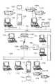
FIG. 1 is a diagram illustrating a case where a network board (NEB) 101 is connected to a
[0011]
A plurality of personal computers (PCs) such as
[0012]
In addition, a
[0013]
More specifically, the network shown in FIG. 1 can use network software such as Novell or UNIX software in order to efficiently communicate between various network members. Although any network software can be used, this embodiment will be described based on a LAN using Novell's NetWare (trademark of Novell, hereinafter omitted) software. A detailed description of this software package is given in the “NetWare User Guide” and “NetWare Supervisor Guide” published by M & T Books, Inc., which were registered in 1990. See also the March 1991 edition of "NetWare Print Server" (Novell Part 100-000892-001) published by Novell.
[0014]
Briefly, the
[0015]
Each of the
[0016]
Typically, a LAN, such as
[0017]
Therefore, as shown in FIG. 1, the
[0018]
The
[0019]
The
[0020]
The
[0021]
A fourth drawback is that only a limited amount of printer status and control information is provided through the
[Network board]
The installation of the
[0022]
As shown in FIG. 2, the
[0023]
The
[0024]
An important factor in NEB design is the function of accessing the printer control status from the
[0025]
FIG. 2 is a cross-sectional view showing a state where the
[0026]
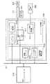
FIG. 3 is a block diagram showing electrical connections among the
[Physical arrangement of NEB]
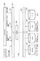
FIG. 4 is a diagram showing the size of the components of the
[0027]
FIG. 5 is a diagram showing in more detail the
[Configuration of NEB]
The configuration of the
[0028]
The network and
[0029]
The
[0030]
The NEB
[0031]
The NEB
[0032]
The central processing unit of
[0033]
The
[0034]
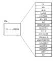
FIG. 7 is a diagram illustrating an example of the number of code blocks, that is, modules, stored in the
[0035]
The PRETASK module identifies which frame type is associated with which of the various protocol stacks above, as shown below. Since
Novell's IPX / SPX protocol stack is included in
CPRINTSERVER is executed exclusively by the Novell print server application. This module provides a self-generated print banner, notification of completion and exception status to the user, and transmission of print data and information commands to the printer engine. This is different from the Novell print server in that the CPRINTSERVER only operates the local printer (that is, the
[0036]
The TCP / IP protocol stack has user datagram protocol (UDP), reverse address resolution protocol (RARP), and BootP auxiliary in its interior. INTERRUPT is an interrupt handler for TCP / IP tasks, and TIMERTICK is a timer tick for UNIX TCP / IP network tasks. LPRINTSERVER is a TCP / IP print server application and owns a print data channel for continuing a print job.
[0037]
The CPSOCKET program works for all protocol stacks. The program responds to connection requests, data download requests, service requests from remote devices, etc., and provides status and control to other tasks via intermediate processing communications. Since a typical CPSOCKET has a status and control channel between the
[0038]
MONITOR is a dedicated multitask monitor that performs task generation, task termination, and microprocessor dispatch. MONITOR also has memory management submodules MEMGET and MEMFREE. RESIDENT is a block of routines that provide general services such as NVRAM read and write, FLASH code, ROM-based debugger, hardware timer ticks, and other basic functions. POST is a self-diagnosis module at startup, and checks the integrity of NEB hardware and software at the start of power supply.
[0039]
[0040]
All communication between the
[0041]
Generally speaking, the
[NEB functionality]
Broadly speaking,
[0042]
Thus, the
[0043]
All of the network traffic enters the
[0044]
All software modules executed by the
[0045]
For example, since many communication protocol types are broadcast on the
[0046]
Reprogramming
[0047]
The
[0048]
As explained above, access to shared
[0049]
Most of the shared
[0050]
With this configuration, the write processor can determine whether there is a writable area in the memory by comparing the put pointer and the get pointer with each other, and the read processor has remaining data to read. It can be determined whether or not. In order to reduce the number of shared memory conflicts between the two processors, the
[0051]
The
[Automatic detection of network hardware connection]
Network interface cards typically provide several different types of physical connection means for connecting network cables to a LAN. For example, the
[0052]
Typically, when a network interface card is connected to a LAN through one of several connectors, users who set up or change the connection to the LAN will be able to exchange data through the appropriate connector. Not only must the LAN cable be plugged into the appropriate connector, but the hard switch or “jumpers” position must be physically changed.
[0053]
However, it is possible for the user to forget to change the jumper or to change the jumper so that it does not match the set connection. In such cases, it goes without saying that the card cannot talk to the network at all. This results in a waste of time, manpower, and computer resources to discriminate and correct these problems. A network interface card that automatically senses which connector is connected to the LAN and exchanges data through that connector makes the connection setup and / or change process much more efficient.
[0054]
The present invention automatically detects hardware as described above by testing, checks the connectivity of each connector to the network, and selects one connector so that network communication is performed on the selected connector and board. To be done between processors. In general, the network control unit includes a first detection unit that detects that the first connector is electrically connected to the network, and a “jabber” that indicates that the second connector is improperly terminated. (Jabber) "bits and a first register readable by the processor. A second register, also readable by the processor, is a "good-link" bit that indicates that the first detector has detected that the first connector is electrically connected to the network. Remember. Also, a control register that can be written by the processor stores selection bits. The control register outputs a selection signal according to the stored selection bit.
[0055]
The microprocessor performs the selection process controlled by the software by the following method. That is, (1) a selection bit is written to the control register so that a selection signal for selecting the first connector (here, RJ-45, connector 301) is output, and (2) a link good bit is read from the second register. , (3) retains the state of the selected bit when the link good bit indicates electrical connection to the network, and (4) the second connector (when the link good bit does not indicate electrical connection to the network) Here, a selection bit is written to the control register so as to output a selection signal for selecting UTP, connector 302), (5) the jabber bit is read from the first register, and (6) the jabber bit is electrically connected to the second connector. If it is not indicated that the termination is inappropriate, the state of the selected bit is retained. (7) The jabber bit is electrically connected to the second connector. To indicate that the switching termination conditions, selecting process is repeated. This procedure allows it to perform a selection process after the board has been powered on for some time. Once selected, it is held while power is supplied to the board.
[0056]
Specifically, referring to FIG. 8, the BNC connector 302 (via the transceiver 171) and the RJ-45
[0057]
When the RJ-45
[0058]
A BNC connector, such as
[0059]
The
[0060]
Since there is an inherent delay in switching the N-channel devices constituting the link
[0061]
Then, the program reads the jabber register 514 (step S908). If the state of the
[0062]
In this way, the
[0063]
In the present embodiment, the selected hardware connection is maintained during the current cycle in which power is being supplied. It is possible to run software that senses when the hardware connection is no longer valid after a selection has been made during the current cycle in which power is being supplied, allowing the selection process to be repeated and changing the connector. It is. This allows dynamic switching from one connection to another.
[Network protocol sensor]
In order to ensure proper operation in multi-protocol systems and to avoid making inappropriate assumptions about the protocols and frame types used on the network,
[0064]
10 to 14 are diagrams for explaining this process. FIG. 10 is a flowchart showing processing steps performed by the
[0065]
In step S1001, the
[0066]
In step S1002, the
[0067]
In step S1003, the
[0068]
Processing proceeds to step S1005, where MLID and LSL monitor network traffic. In particular, in step S1005, the network monitors the broadcast traffic means and observes that the destination of the traffic has not been determined (that is, the destination can be anywhere). Typically, broadcast traffic is identified by a global specification such as a destination MAC address, for example an address with 12 hexadecimal Fs in a row. Until LAN broadcast traffic is detected, PRETASK does nothing.
[0069]
At this point during execution of PRETASK, the relationship between the various software modules is as shown in FIG. As can be seen, a plurality of network devices, such as
[0070]
[0071]
If LAN broadcast traffic is detected, the process advances to step S1006, and the LSL supplies a frame packet to PRETASK. In step S1007, PRETASK decodes the protocol header of the frame in order to identify the protocol used in the frame packet. The offset to this header depends on the frame type used by the protocol. The table below contains hexadecimal values and several examples of protocol headers for identifying different protocols.
[0072]
In step S1008 of FIG. 10, PRETASK cancels the registration of the frame type just received from the LSL. Therefore, as shown at 189a in FIG. 12, PRETASK cancels the registration of 802.2.
Step S1008 shows a case where registration is canceled in all cases, but it may be more preferable not to cancel registration. In particular, if each different protocol has a list of acceptable frame types for it. Examples of acceptable frame types for IPX / SPX and TCP / IT are shown below.
[0073]
In step S1009, PRETASK loads a protocol stack corresponding to the protocol decoded in step S1007. In the example of FIG. 12, since the IPX / SPX protocol has been decoded, PRETASK loads the IPX / SPX protocol stack from the
[0074]
In step S1010, the newly loaded protocol stack is registered in the LSL, for example, as shown in FIG. As shown in the figure, the IPX / SPX protocol stack registers 802.2 with the LSL. By registering as described above, IPX / SPX informs LSL to provide all frame packets that match the registered frame type (here 802.2) to the newly loaded protocol stack. To do.
[0075]
PRETASK then returns to step S1005 to continue observing the network for broadcast traffic. When LSL finds frame packets that match the remaining frame types registered by PRETASK, LSL supplies these frame types to PRETASK to perform the processing shown in FIG. Thus, each time an additional frame type is found, such as a frame type associated with the TCP / IP protocol, these frames are processed by PRETASK so that the appropriate protocol stack is loaded from
[0076]
Further, as shown in FIG. 14, since the protocol stack is already loaded, the operation on the network is started. In particular, PRETASK is completely passive and does not broadcast network communications, whereas IPX / SPX broadcasts SAP requests for it. Other protocol tasks loaded by PRETASK may broadcast their associated requests. For example, when the TCP / IP protocol stack is loaded, it broadcasts RARPS to get its address from the nearest network server.
[Smart Flash]
As local area networks have become more complex, there has been a need to upgrade network interface cards such as
[0077]
A typical PC is connected to two or more LANs. For example, as shown in FIG. 15, the
[0078]
When reprogramming a particular NEB, the network administrator must run a program from the
[0079]
Since the network supervisor may oversee more than one network, each containing several reprogrammable boards connected to the network, the supervisor will send the appropriate image data to the target NEB. I have to confirm that. Therefore, if the network supervisor wants to reprogram the
The result of downloading incompatible image data can be destructive. For example, if the network supervisor mistakenly downloads the Token-ring image data to the
[0080]
In order to avoid such disastrous consequences when incompatible image data is downloaded,
[0081]
More specifically, the NIF block contains permanent adapter specific configuration information and is specific to each individual NEB. As an example, the NIF block occupies 32 bytes of the memory space in the flash EPROM 413 and is divided into 4 banks of 8 bytes each. As shown in FIG. 16, the NIF block includes a MAC address information bank, a board version / identification information bank, a component identification information bank, and a general information bank.
[0082]
The MAC address information bank, as its name suggests, stores a unique MAC address for the board. The board version and identification information bank is further divided into four banks. Because network interface cards other than NEBs can be connected to the LAN, the product category bank identifies the type of product connected to the LAN, and the board modification bank identifies the modification number of the product.
[0083]
The network physical media bank is further divided into two banks. These are the physical network bank that identifies the physical medium in which the board is used (eg Ethernet, Token-ring, FDDI, etc.) and the physical connector that the board assists (eg 10baseT for an Ethernet network) In the case of 10base2, 10base5, and Token-ring, it is an auxiliary connection bank that identifies the type of UTP and STP). The host interface method bank identifies the type of interface to the peripheral device (such as
[0084]
The component identification information bank is also divided into several smaller banks. These banks identify the size and fineness of the ROM, DRAM and NVRAM on the board, and the erasability of the ROM. In addition, a network control unit (DP83902 chip for Ethernet, TI389C25 for Token-ring) and a host control unit (arbitrated shared RAM, NCR53C90A SCSI controller or NCR53C80 SCSI controller) are identified. The CPU identification bank stores the processor type and clock speed. Finally, the general information bank stores other data for identifying additional configuration attributes for the board, such as the hardware modification level.
[0085]
Next, a description will be given with reference to the flowchart of FIG. When the CPFLASH program on the network supervisor's PC scans the bindery, reprogramming of the
[0086]
Once new image data is downloaded to
[0087]
The software reprogramming module then refers to the information stored in the current image data NIF block (information copied to DRAM 175) to confirm that the new image data is compatible. Is compared with the information stored in the new frameware image NIF block to check the compatibility of the image data (step S1406). Since the NIF block has a large amount of information about the
[0088]
The initial compatibility check includes a network media configuration check to determine whether the new image data is the correct network media type, by referring to data stored in the physical network bank of the NIF block. Similarly, a second compatibility check is performed by comparing the new image data with the data stored in the host interface method bank and the host interface controller bank of the NIF block, and the new image data is the appropriate host (e.g. A host interface configuration check for determining whether the image data is to be interfaced to a shared RAM or SCSI).
[0089]
The third compatibility check is done by referring to the product category bank and board modification bank of the NIF block and comparing that data to the new image data, because the new image data is for the type of board with the built-in EPROM. Product configuration check to determine whether or not A processor configuration check can also be performed by referring to the CPU bank of the NIF block to determine whether the new image data is compatible with the processor on the board. In addition, the memory configuration check will update the data stored in the ROM bank, DRAM bank, and / or NVRAM bank of the NIF block to determine if the new image data is compatible with the board's memory. This can be done by comparing with image data. Other compatibility checks can be performed by using other information stored in the NIF block.
[0090]
If it is determined that the new image data is incompatible, the current protocol stack is reactivated (steps S1407 and S1408), and an error is reported to the
[0091]
Conversely, if the new image data is compatible, the board-invariant part of the NIF block of the new image data is replaced by the NIF block of the current image data to retain board-specific information (MAC address, board modification number, etc.). Are replaced by corresponding portions (steps S1407 and S1410). The program then erases the current image data from the
[0092]
With this configuration, even when incompatible image data is downloaded from the
[Arbitration equipment]
FIGS. 18 to 20 are diagrams illustrating arbitration of the shared
[0093]
FIG. 18 shows a printer address / data bus (A / D bus) 701, a print address latch enable (ALE) signal 702, a printer data enable (DEN) signal 704, a
[0094]
FIG. 15 also shows a NEB address / data bus (A / D bus) 711, a
[0095]
As described above, the
[0096]
[0097]
Similarly, the
[0098]
The shared
[0099]
The
[0100]
The PACK access permission signal for the printer is input to the
[0101]
The shared
[0102]
With the configuration shown in FIG. 19, even if the
[0103]
Returning to FIG. 18, the
[0104]
More specifically, the NEB access permission signal NACK is supplied to the
[0105]
Buffer 737 buffers address information from
[0106]
The
[0107]
Therefore, in summary, when the NEB receives permission to access the shared
[0108]
If the
[0109]
Specifically, for the address information latched by the
[0110]
The
[0111]
The handling of data information varies depending on whether reading or writing is requested by the
[0112]
The upper byte of the data information on the printer A /
[0113]
When the
[0114]
Therefore, in summary, when the
[0115]
The OR
FIG. 20 is a timing diagram showing the timing of signals input to the arbiter
[0116]
The NEB side corresponds to the address space of the shared
[Reduction of bus contention in shared memory]
As described above, the arbiter
[0117]
FIG. 21 is a diagram showing how usable memory in the
[0118]
As shown in FIG. 21, the
[0119]
Data is written to the ring buffer in 256-byte blocks along with a put pointer and a get pointer that indicate where the next block begins. For example, in FIG. 21, the put pointer indicates a
[0120]
Thus, when transmitting data from one processor to the other using a ring buffer, the receiving processor tracks the transmitting processor "around the ring" and reads the written data. The receiving processor is limited by the speed of the printer it is operating on, and the sending processor usually writes at a faster rate than the receiving processor reads. There is a tendency to go around the ring and catch up with the later get pointer. In such a case, the sending processor waits until the ring buffer memory space becomes available. During this waiting time, in a conventional system, the sending processor periodically reads and compares the put pointer and the get pointer to determine whether space is available. Such polling by the sending processor slows down the processing speed of the receiving processor because the sending processor must access the shared memory and read the pointer value. This obstructs access by the printer and degrades the overall system functionality.
In the
[0121]
FIG. 22 shows a procedure in which the transmitting processor (that is, the NEB microprocessor 173) of the
[0122]
Accordingly, in step S1903, the
[0123]
In step S 1906, the put pointer and the get pointer are read from the
[0124]
On the other hand, if it is determined in step S1907 that the put pointer is not equal to any of the divided indexes, the process proceeds to step S1912, and the
[0125]
When the processor on the receiving side reads a data block including a notification reception issue command from the shared memory, it issues a reception notification. Specifically, referring to FIG. 23, the receiving processor starts retrieving data by reading the values of the get pointer and the put pointer from the shared memory (step S2001). If there is data to be retrieved (step S2002), the receiving processor reads the data block from the memory location specified by the get pointer (steps S2002 to S2004), and updates the value of the get pointer (step S2005). ).
[0126]
Then, the receiving processor executes all commands included in the data block, such as a reception notification issue command, for example (step S2006). The receiving processor issues this reception notification as an interrupt to the transmitting processor by writing 1 bit to the interrupt control register 450 which is a part of the arbiter
[0127]
As a result, when the ring buffer is divided into two parts, the sending processor writes the block to only half of the ring buffer at a time, and checks whether the receiving processor has read the other half, For each index, stop accessing the shared memory until the receiving processor catches up. In another example, the ring can be further subdivided when two ring segments are insufficient. In these cases, an additional index can be used as shown in FIGS. 24 (a) to (c).
[0128]
With this configuration, since the
[Serial port]
As described above, the
[0129]
Because the
[0130]
FIG. 25 shows the configuration of the serial port where the signal on the receive channel is sent to the non-maskable interrupt (NMI) pin of the
[0131]
More specifically, as shown in FIG. 25, the serial port configuration of the present invention includes a non-maskable interrupt (NMI)
[0132]
The
[0133]
The
[0134]
The NMI enable
[0135]
The
FIG. 26 is a flowchart showing the serial port processing in the serial reception mode. The processing steps in FIG. 26 are executed by the
[0136]
In step S2301, the
[0137]
On the other hand, when the NMI signal is received at the
[0138]
Returning to FIG. 26 again, the description will be continued. After the
[0139]
When 8-bit data is received, the process proceeds to step S2309, and the interrupt handling process stores the 8-bit byte data received by the receiving
[0140]
In step S2311, the
[0141]
Accordingly, in step S2311, it is determined whether the byte received at the serial port connector is a request for an asynchronous interrupt. For example, using an already established rule, it can be determined that sending an exclamation point ("!") Identifies an asynchronous interrupt. In this case, the
[0142]
Therefore, when trouble occurs due to asynchronous interruption, the troubleshooter can analyze the current state of the NEB. As the NMI signal is generated by the first bit of serial communication, an asynchronous interrupt can even interrupt a very tightly tied microprocessor loop to allow analysis of the system state A debugging session can be started.
[0143]
Conversely, if the 8-bit byte stored in step S2309 does not request an asynchronous interrupt, the
[0144]
FIG. 28 is a diagram illustrating a processing flow in the transmission mode of the software serial port, and FIG. 29 is a diagram illustrating a signal appearing at the
In step S2401, the
[0145]
The process proceeds to step S2402, and the
[0146]
The above description has been made with reference to specific examples, but the present invention is not limited to the above embodiments. It will be apparent to those skilled in the relevant art that many variations are possible in light of the above description without departing from the spirit and scope of the invention.
[0147]
【The invention's effect】
As described above, according to the present invention, it is possible to automatically sense which connector is connected to the network, and to transmit / receive data using the connector connected to the network. The possibility of trying to communicate with the network through a connector that is not connected is eliminated.
[Brief description of the drawings]
FIG. 1 is a diagram showing a local area network and a wide area network to which network boards are connected.
FIG. 2 is a cross-sectional view showing a network board fitted in a Canon LBP 1260 laser printer.
FIG. 3 is a block diagram illustrating a network board connected between a printer and a local area network.
FIG. 4 is a diagram illustrating an arrangement of components on a network board.
FIG. 5 is a diagram showing a face plate of a network board.
FIG. 6 is a block diagram illustrating functions of a network board.
FIG. 7 is a diagram showing an example of software modules stored in a flash EPROM.
FIG. 8 is a block diagram showing a configuration for determining which connector is connected to the network.
FIG. 9 is a flowchart illustrating a method for determining which connector is connected to a network.
FIG. 10 is a flowchart showing the operation of the PRETASK software module.
FIG. 11 is a diagram showing possible relationships between various network modules.
FIG. 12 is a diagram showing possible relationships between various network modules.
FIG. 13 illustrates possible relationships between various network modules.
FIG. 14 shows possible relationships between various network modules.
FIG. 15 is a block diagram showing a PC connected to an Ethernet local area network and a Token-ring local area network.
FIG. 16 is a diagram showing the contents of a network information file block for storing structure information.
FIG. 17 is a flowchart showing flash EPROM reprogramming.
FIG. 18 is a block diagram of a memory arbitration device.
FIG. 19 is a block diagram showing an example of a preferred configuration of a shared memory arbiter of a memory arbitration device.
FIG. 20 is a diagram illustrating timings of signals supplied to the memory arbitration device.
FIG. 21 is a diagram illustrating a configuration of a shared memory.
FIG. 22 is a flowchart showing a procedure related to writing to a shared memory.
FIG. 23 is a flowchart showing a procedure related to reading from a shared memory;
FIG. 24 is a diagram illustrating another example of the configuration of the shared memory.
FIG. 25 is a block diagram of a serial port.
FIG. 26 is a flowchart showing a procedure related to transmission / reception of serial communication via a serial port.
FIG. 27 is a diagram illustrating signal timing in a serial transmission / reception mode.
FIG. 28 is a flowchart showing a procedure related to transmission / reception of serial communication via a serial port.
FIG. 29 is a diagram illustrating signal timing in a serial transmission / reception mode.
[Explanation of symbols]
173 NEB Microprocessor
510 Network control unit
511 selector
512 Link good detection part
513 jabber detector
514 Jabber Register
520 NEB control logic
521 Control register
522 Link good register
Claims (3)
Translated fromJapaneseバスに接続され、前記バスと選択された前記第1及び第2のコネクタのいずれか一方との間でネットワーク通信を行い、前記第1のコネクタがネットワークに電気的に接続しているか否かを検出する第1検出部と、前記第2のコネクタが適切に終端していないことを示すジャバービットを記憶する前記バスを介して読み込み可能な第1レジスタと、前記第1及び第2のコネクタのいずれか一方を選択する選択信号に従って前記第1及び第2のコネクタのいずれか一方を選択するセレクタとを有し、前記第1及び第2のコネクタに接続するネットワーク制御部と、
前記第1のコネクタがネットワークに電気的に接続していることを前記第1検出部が検出したことを示すリンク良好ビットを記憶するための、前記バスを介して読み込み可能な第2レジスタと、
内部に記憶された選択ビットに基づいて選択信号を前記セレクタに対して出力するための、前記バスを介して書き込み可能な制御レジスタと、
(1)前記第1のコネクタを選択する選択信号を前記セレクタに対して前記制御レジスタに出力させるために、前記バスを介して前記制御レジスタに選択ビットを書き込み、(2)前記バスを介して前記第2レジスタから前記リンク良好ビットを読み出し、(3)前記リンク良好ビットがネットワークへの電気的な接続を示すときに、前記選択ビットの状態を保持し、(4)前記リンク良好ビットがネットワークへの電気的な接続を示さない時に、前記第2のコネクタを選択する選択信号を前記セレクタに対して前記制御レジスタに出力させるために、前記バスを介して前記制御レジスタに選択ビットを書き込み、(5)ジャバービットを前記第1レジスタから読み込み、(6)前記ジャバービットが前記第2のコネクタの電気的に適切な終端を示す場合に、前記選択ビットの状態を保持し、(7)前記ジャバービットが前記第2のコネクタの電気的に不適切な終端を示す場合には(1)に戻る、前記バスに接続され、前記バスを介してネットワーク通信の送受信を行うプロセッサーとを含むことを特徴とするネットワーク通信装置。A network communication device having first and second connectors each connectable to a network,
Is connected to the bus, the performs network communication with the one bus with any of the selected firstandsecond connectors, whether thefirst connector is electrically connected to the network a first detector for detecting a first register readable through the bus for storing the jabber bit indicates that thesecond connector is not properly terminated, the first and second connectorA selectorfor selecting one of the first and second connectors according to a selection signal for selectingeither one, and a network control unit connected to the first and second connectors;
A second register readable throughthe bus for storing a good-link bit indicates that the first detector detects that thefirst connector is electrically connected to the network,
For outputting a selection signalto the selector based on the selection bits stored therein, and writable control registers viathe bus,
(1) a selection signal for selecting saidfirst connector inorder to outputto the control register to the selector, a write selection bit to the control register viathe bus, through the (2)the bus Reading the link good bit from the second register; (3) holding the state of the selected bit when the link good bit indicates an electrical connection to the network; and (4) the link good bit is the network. when showing no electrical connection to a selection signal for selecting said second connector inorder to outputto the control register to the selector, a write selection bit to the control register viathe bus, (5) the jabber bit read from the first register, (6) the jabber bit is thesecond connector electrically appropriate end of To indicate, to maintain the state of the selection bit, (7) when the jabber bit indicates improper electrical termination of thesecond connectorreturns to (1), connected tosaid bus , network communication device which comprises a processor for sending and receiving network communications viathe bus.
Applications Claiming Priority (2)
| Application Number | Priority Date | Filing Date | Title |
|---|---|---|---|
| US08/336,662US5701411A (en) | 1994-11-04 | 1994-11-04 | Automatic detection of network hardware connection |
| US08/336662 | 1994-11-04 |
Publications (2)
| Publication Number | Publication Date |
|---|---|
| JPH08255118A JPH08255118A (en) | 1996-10-01 |
| JP3796282B2true JP3796282B2 (en) | 2006-07-12 |
Family
ID=23317103
Family Applications (1)
| Application Number | Title | Priority Date | Filing Date |
|---|---|---|---|
| JP28616195AExpired - Fee RelatedJP3796282B2 (en) | 1994-11-04 | 1995-11-02 | Network communication equipment |
Country Status (4)
| Country | Link |
|---|---|
| US (1) | US5701411A (en) |
| EP (1) | EP0710912B1 (en) |
| JP (1) | JP3796282B2 (en) |
| DE (1) | DE69529451T2 (en) |
Families Citing this family (30)
| Publication number | Priority date | Publication date | Assignee | Title |
|---|---|---|---|---|
| US5819110A (en)* | 1995-06-05 | 1998-10-06 | Ricoh Company, Ltd. | System for determining whether connection or connectionless modes of communication should be used to transmit information between devices in accordance with priorities of events |
| US6098116A (en)* | 1996-04-12 | 2000-08-01 | Fisher-Rosemont Systems, Inc. | Process control system including a method and apparatus for automatically sensing the connection of devices to a network |
| US5892926A (en)* | 1996-12-30 | 1999-04-06 | Compaq Computer Corporation | Direct media independent interface connection system for network devices |
| US5980078A (en)* | 1997-02-14 | 1999-11-09 | Fisher-Rosemount Systems, Inc. | Process control system including automatic sensing and automatic configuration of devices |
| US5935249A (en)* | 1997-02-26 | 1999-08-10 | Sun Microsystems, Inc. | Mechanism for embedding network based control systems in a local network interface device |
| US6353927B1 (en)* | 1997-10-14 | 2002-03-05 | Lucent Technologies Inc. | Data download technique into installed memory |
| US5949335A (en)* | 1998-04-14 | 1999-09-07 | Sensormatic Electronics Corporation | RFID tagging system for network assets |
| US6707567B1 (en)* | 1998-05-20 | 2004-03-16 | Ricoh Company, Ltd. | Supervising system for image forming apparatus and method thereof |
| US6725278B1 (en)* | 1998-09-17 | 2004-04-20 | Apple Computer, Inc. | Smart synchronization of computer system time clock based on network connection modes |
| US6408334B1 (en) | 1999-01-13 | 2002-06-18 | Dell Usa, L.P. | Communications system for multiple computer system management circuits |
| US6718381B1 (en) | 1999-01-26 | 2004-04-06 | Dell Usa L.P. | Removal notification for a computer system |
| US6665724B2 (en)* | 1999-07-20 | 2003-12-16 | Canon Kabushiki Kaisha | Method for automatically delaying initialization of a protocol stack within a network interface |
| US6711629B1 (en) | 1999-10-18 | 2004-03-23 | Fisher-Rosemount Systems, Inc. | Transparent support of remote I/O in a process control system |
| US7216347B1 (en) | 2000-04-17 | 2007-05-08 | International Business Machines Corporation | Method and apparatus for prioritizing print jobs from multiple printer input channels |
| US7589849B2 (en)* | 2000-04-17 | 2009-09-15 | Inforprint Solutions Company, Llc | Method and apparatus for providing printer recognition and management of a print job entity |
| TWI237966B (en)* | 2000-09-21 | 2005-08-11 | Via Tech Inc | Method for dynamically selecting physical layer |
| US20020108058A1 (en)* | 2001-02-08 | 2002-08-08 | Sony Corporation And Sony Electronics Inc. | Anti-theft system for computers and other electronic devices |
| US7552216B2 (en)* | 2001-03-27 | 2009-06-23 | Lexmark International, Inc. | Method of sharing a printer |
| US20030055958A1 (en)* | 2001-09-20 | 2003-03-20 | Russell Richard Francis | Method for automatically creating network printer ports on a workstation |
| US6653845B2 (en)* | 2002-02-25 | 2003-11-25 | Daimlerchrysler Corporation | Addressable open connector test circuit |
| US7366799B2 (en) | 2002-03-06 | 2008-04-29 | Pharos Systems International, Inc. | Document processing system including multi-device compatible interface and related methods |
| US7043577B2 (en)* | 2002-08-27 | 2006-05-09 | General Electric Company | Auto-detecting universal appliance communication controller |
| JP2004171411A (en)* | 2002-11-21 | 2004-06-17 | Hitachi Global Storage Technologies Netherlands Bv | Data storage device and buffer memory management method |
| JP2004289561A (en)* | 2003-03-24 | 2004-10-14 | Sony Corp | Management method of network connection, and electronic equipment |
| JP4880883B2 (en)* | 2004-07-14 | 2012-02-22 | キヤノン株式会社 | COMMUNICATION DEVICE CONTROL METHOD, COMMUNICATION DEVICE, AND COMMUNICATION DEVICE CONTROL PROGRAM |
| JP2006039982A (en) | 2004-07-28 | 2006-02-09 | Canon Inc | Information processing apparatus control method, information processing apparatus, and information processing apparatus control program |
| JP4725066B2 (en)* | 2004-09-30 | 2011-07-13 | セイコーエプソン株式会社 | Printing device monitoring system, network board, and printing device monitoring method |
| US8082368B2 (en)* | 2006-04-21 | 2011-12-20 | Infortrend Technology, Inc. | Display device for indicating connection statuses of a communication channel provided between two systems and method thereof |
| TWI569604B (en)* | 2015-01-21 | 2017-02-01 | 智邦科技股份有限公司 | Network switch system and its operation method |
| CN111402784B (en)* | 2020-03-10 | 2022-02-18 | 苏州仰邦软件科技有限公司 | Method for stabilizing network operation of LED controller and display screen control system thereof |
Family Cites Families (10)
| Publication number | Priority date | Publication date | Assignee | Title |
|---|---|---|---|---|
| US3990024A (en)* | 1975-01-06 | 1976-11-02 | Xerox Corporation | Microstrip/stripline impedance transformer |
| JPH02294757A (en)* | 1989-05-09 | 1990-12-05 | Ricoh Co Ltd | Input/output apparatus |
| US5142269A (en)* | 1991-04-01 | 1992-08-25 | Charles T. Rush | Electronic component theft sensor and security system |
| US5319785A (en)* | 1991-06-28 | 1994-06-07 | Digital Equipment Corporation | Polling of I/O device status comparison performed in the polled I/O device |
| US5410535A (en)* | 1992-07-02 | 1995-04-25 | Digital Equipment Corporation | Automatic selection of an interface for ethernet stations |
| US5444856A (en)* | 1992-07-07 | 1995-08-22 | Intel Corporation | Apparatus and method for switching ethernet media type |
| US5696899A (en) | 1992-11-18 | 1997-12-09 | Canon Kabushiki Kaisha | Method and apparatus for adaptively determining the format of data packets carried on a local area network |
| US5611046A (en)* | 1992-11-18 | 1997-03-11 | Canon Kabushiki Kaisha | Method and apparatus for interfacing a peripheral to a local area network |
| US5406260A (en)* | 1992-12-18 | 1995-04-11 | Chrimar Systems, Inc. | Network security system for detecting removal of electronic equipment |
| US5513370A (en)* | 1992-12-22 | 1996-04-30 | National Semiconductor Corporation | Twisted pair and attachment unit interface (AUI) coding and transceiving circuit with full duplex, testing, isolation, and automatic output selection |
- 1994
- 1994-11-04USUS08/336,662patent/US5701411A/ennot_activeExpired - Lifetime
- 1995
- 1995-10-30DEDE69529451Tpatent/DE69529451T2/ennot_activeExpired - Lifetime
- 1995-10-30EPEP95307706Apatent/EP0710912B1/ennot_activeExpired - Lifetime
- 1995-11-02JPJP28616195Apatent/JP3796282B2/ennot_activeExpired - Fee Related
Also Published As
| Publication number | Publication date |
|---|---|
| JPH08255118A (en) | 1996-10-01 |
| DE69529451D1 (en) | 2003-02-27 |
| DE69529451T2 (en) | 2003-10-02 |
| EP0710912B1 (en) | 2003-01-22 |
| US5701411A (en) | 1997-12-23 |
| EP0710912A1 (en) | 1996-05-08 |
Similar Documents
| Publication | Publication Date | Title |
|---|---|---|
| JP3651987B2 (en) | Reprogrammable network communication device and method for reprogramming network communication device | |
| JP3796282B2 (en) | Network communication equipment | |
| JP3535634B2 (en) | Network protocol determination method, network board, and peripheral device | |
| US5548728A (en) | System for reducing bus contention using counter of outstanding acknowledgement in sending processor and issuing of acknowledgement signal by receiving processor to indicate available space in shared memory | |
| JP3689463B2 (en) | Arbitration device | |
| EP0835485B1 (en) | Network board which responds to status changes of its installed peripheral by generating a testpage | |
| US5828863A (en) | Interface device connected between a LAN and a printer for outputting formatted debug information about the printer to the printer | |
| US5935262A (en) | Outputting a network device log file | |
| US5606671A (en) | Serial port using non-maskable interrupt terminal of a microprocessor | |
| US5852746A (en) | System for transmitting a message using status button to system administrator by using a signal comprising predetermined number of changes effected over a period | |
| EP1234235B1 (en) | Method and apparatus for remotely debugging computer software over a serial bus | |
| Carboney | USB97C102 Programmers Reference Guide | |
| HK1013751A (en) | Method and device for transmitting a message to a lan administrator | |
| Carboney | APPLICATION NOTE 8.19 USB97C102 Programmers Reference Guide |
Legal Events
| Date | Code | Title | Description |
|---|---|---|---|
| A131 | Notification of reasons for refusal | Free format text:JAPANESE INTERMEDIATE CODE: A131 Effective date:20050218 | |
| A521 | Request for written amendment filed | Free format text:JAPANESE INTERMEDIATE CODE: A523 Effective date:20050419 | |
| A131 | Notification of reasons for refusal | Free format text:JAPANESE INTERMEDIATE CODE: A131 Effective date:20051114 | |
| A521 | Request for written amendment filed | Free format text:JAPANESE INTERMEDIATE CODE: A523 Effective date:20060113 | |
| TRDD | Decision of grant or rejection written | ||
| A01 | Written decision to grant a patent or to grant a registration (utility model) | Free format text:JAPANESE INTERMEDIATE CODE: A01 Effective date:20060331 | |
| A61 | First payment of annual fees (during grant procedure) | Free format text:JAPANESE INTERMEDIATE CODE: A61 Effective date:20060417 | |
| R150 | Certificate of patent or registration of utility model | Free format text:JAPANESE INTERMEDIATE CODE: R150 | |
| FPAY | Renewal fee payment (event date is renewal date of database) | Free format text:PAYMENT UNTIL: 20090421 Year of fee payment:3 | |
| FPAY | Renewal fee payment (event date is renewal date of database) | Free format text:PAYMENT UNTIL: 20100421 Year of fee payment:4 | |
| FPAY | Renewal fee payment (event date is renewal date of database) | Free format text:PAYMENT UNTIL: 20110421 Year of fee payment:5 | |
| FPAY | Renewal fee payment (event date is renewal date of database) | Free format text:PAYMENT UNTIL: 20120421 Year of fee payment:6 | |
| FPAY | Renewal fee payment (event date is renewal date of database) | Free format text:PAYMENT UNTIL: 20130421 Year of fee payment:7 | |
| FPAY | Renewal fee payment (event date is renewal date of database) | Free format text:PAYMENT UNTIL: 20130421 Year of fee payment:7 | |
| FPAY | Renewal fee payment (event date is renewal date of database) | Free format text:PAYMENT UNTIL: 20140421 Year of fee payment:8 | |
| LAPS | Cancellation because of no payment of annual fees |