JP3793464B2 - Semiconductor memory device - Google Patents
Semiconductor memory deviceDownload PDFInfo
- Publication number
- JP3793464B2 JP3793464B2JP2002011910AJP2002011910AJP3793464B2JP 3793464 B2JP3793464 B2JP 3793464B2JP 2002011910 AJP2002011910 AJP 2002011910AJP 2002011910 AJP2002011910 AJP 2002011910AJP 3793464 B2JP3793464 B2JP 3793464B2
- Authority
- JP
- Japan
- Prior art keywords
- data
- semiconductor memory
- flash memory
- writing
- write
- Prior art date
- Legal status (The legal status is an assumption and is not a legal conclusion. Google has not performed a legal analysis and makes no representation as to the accuracy of the status listed.)
- Expired - Lifetime
Links
Images


Landscapes
- Memory System (AREA)
- Information Retrieval, Db Structures And Fs Structures Therefor (AREA)
- Read Only Memory (AREA)
Description
Translated fromJapanese【0001】
【産業上の利用分野】
本発明はフラッシュメモリを用いた半導体記憶装置に関し、特にフラッシュメモリを用いた半導体ディスク装置などに連続してデータの書き込みをすることに関する。
【0002】
【従来の技術】
本発明は、例えば、複数ビットを1ワードとして、ワード単位に読み出し書き込み可能で、チップ単位あるいは複数ワード単位に電気的に消去可能なフラッシュEEPROMを複数個搭載し、上記フラッシュメモリに連続してデータの書き込みを行なう装置において、1ワードのデータを上記書き込み装置に搭載された任意の前記フラッシュメモリに書き込み、書き込みが行なわれた上記フラッシュメモリが次の1ワードのデータを書き込み可能となる一定時間の間に、前記装置に搭載された書き込みが行なわれている前記フラッシュメモリとは別のフラッシュメモリに1ワードのデータを書き込むことを特徴とする。
【0003】
従来技術に係るコマンド制御方式で書き込みや消去を行うフラッシュメモリの、データ書き込みのタイミング波形を図8に示す。図中Vccはフラッシュメモリの電源電圧であり、常時+5Vが印加されている。Vppは書き込み電源であり、フラッシュメモリへデータの書き込みを行うとき電源電圧Vccより高い電位を印加する。アドレスはフラッシュメモリのデータの書き込み領域をバイト単位に指定するものである。OEはアウトプットイネーブル信号であり、フラッシュメモリからデータの読み出しを行う際にLowとし、その他の時はHighとする。CEはチップイネーブル信号であり、フラッシュメモリにコマンドやデータの読み出し書き込みを行うときLowとする。また、本フラッシュメモリのCEはライトイネーブル信号も兼ねており、Vppが高電位でかつOEがHighの時OEの立上りでデータが書き込まれる。I/O7およびI/O0〜I/O6はデータ線である。続いて、フラッシュメモリに1バイトのデータを書き込むときの動作を示す。まず、CEの立上りのタイミングでデータ線上のコマンドをフラッシュメモリに書き込む。このコマンドはフラッシュメモリに1ワードのデータの書き込みの開始を知らせる、ライトセットアップコマンドである。このコマンドの書き込みの後、CEの立上りのタイミングでデータ線上のデータをフラッシュメモリに書き込む。このコマンドとデータの書き込み時のCEのLow期間は最小50ナノ秒である。しかし、実際にはフラッシュメモリ内部ではメモリチップへの書き込みが始まったところであり、内部での書き込みが終了するまで次のデータは書き込むことはできない。ここでフラッシュメモリの内部での書き込みが終了するまで、数十マイクロ秒の時間が必要で有り、コマンドと1ワードのデータの書き込みの時間に比較してかなりの時間を要する。そして、この数十マイクロ秒の時間を経て、フラッシュメモリチップの内部での書き込みが終了したことを調べる手段としてステータスポーリングが有る。これはCEとOEをLowにしてI/O7からステータスを読み出してメモリチップ内部での書き込みの終了を判定する。
【0004】
【発明が解決しようとする課題】
上記技術は、複数ワードのデータを連続して書き込む場合かなりの時間を要する。コマンドと1ワードのデータの書き込みは数十ナノ秒から数百ナノ秒程度である。しかし、1ワードのデータを書き込んでからフラッシュメモリチップ内部での書き込みが終了するまでには、数マイクロ秒から数十マイクロ秒の時間が必要であり、この間はフラッシュメモリにアクセスできない。そのため、1ワードのデータを書き込むためのトータルの時間が読みだし時間に比較してかなり遅い。また、複数ワードのデータを連続で書き込む場合、書き込むワード数に比例して書き込み時間が増大する。例えばフラッシュメモリを用いて半導体ディスク装置を構築した場合、数キロワードから数十キロワード、あるいはそれ以上のデータが連続で書き込まれる。そうすると、書き込まれるデータに比例して書き込み時間が増大するため、システム全体として書き込みの転送が遅くなる。
【0005】
本発明の目的は、データの書き込み時間を短縮した半導体記憶装置を提供することである。
【0006】
【課題を解決するための手段】
本発明は、
ページ単位でデータを書き込み、ブロック単位でデータを消去する複数の不揮発性半導体メモリと、
各不揮発性半導体メモリによる前記データの書き込みと前記データの消去とを制御する制御部と、
を備え、
前記制御部は、システムからの1つの書き込みコマンドに応答して、前記システムからの1つの書き込みコマンドに伴う複数セクタ分のデータがセクタ単位で前記各不揮発性半導体メモリに分配されるように、テーブルを参照して、前記システムが管理する論理セクタ番号から前記各不揮発性半導体メモリの物理アドレスを発生し、
前記制御部は、前記複数の不揮発性半導体メモリの1つが、前記複数の不揮発性半導体メモリの1つのために分配されたデータのうちの1ページ分のデータを書き込んでいる間に、前記複数の不揮発性半導体メモリの他の1つのために分配されたデータのうちの1ページ分のデータ及び当該1ページ分のデータのための書き込みコマンドを前記複数の不揮発性半導体メモリの他の1つに与え、
前記制御部は、消去すべき領域が前記ブロック単位で前記複数の不揮発性半導体メモリに分配されるように、前記各不揮発性半導体メモリのブロックのアドレスを発生し、
前記制御部は、前記複数の不揮発性半導体メモリの1つが前記データの消去を実行している間に、前記複数の不揮発性半導体メモリの他の1つに、前記データの消去を実行させるための消去コマンドを与え、
前記制御部は、前記複数の不揮発性半導体メモリへ前記消去コマンドを与えた後に、前記複数の不揮発性半導体メモリのステータスポーリングを行う、
ことを特徴とする半導体記憶装置を提供する。
【0007】
【作用】
本発明に係る半導体記憶装置によれば、前記複数の不揮発性半導体メモリの1つが前記データ消去を実行している間に、プロセッサが、前記複数の不揮発性半導体メモリの他の1つに前記データ消去を実行させるためのコマンドを書き込む。また、プロセッサは、前記複数の不揮発性半導体メモリへの、前記データ消去を実行させるためのコマンドの書き込みが終了した後に、前記データ消去を実行させるためのコマンドを書き込んだ順に前記複数の不揮発性半導体メモリのステータスポーリングを行う。
【0008】
【実施例】
本実施例では、連続したデータの書き込みの場合、連続して同一のフラッシュメモリに書き込むのでなく、他のフラッシュメモリに書き込むように制御する。
【0009】
1ワードのデータをフラッシュメモリに書き込んでから次のデータを書き込むまでに数マイクロ秒から数十マイクロ秒の待ち時間が有る。そのため、連続して書き込みデータが有る場合、この待ち時間の間に連続して他のフラッシュメモリへ1ワードのデータを書き込み続ける。そして、最初に書き込んだフラッシュメモリの待ち時間を過ぎると、最初のフラッシュメモリからステータスポーリングを行ない、次の1ワードのデータを書き込む。この様に、フラッシュメモリの待ち時間の間に他のフラッシュメモリへの書き込みを行う。
【0010】
複数の連続したデータを書き込む用途にフラッシュメモリを用いた場合、本実施例によればフラッシュメモリの低速の書き込みを、装置のトータルで高速化できる。すなわち、フラッシュメモリを半導体ディスク装置に用いた場合、複数の連続したデータが書き込まれる。しかし、連続したデータの書き込みの場合、フラッシュメモリへの書き込みが読み出しに比較して遅いため、トータルの転送速度が低下する。しかし、本実施例によればフラッシュメモリの書き込みが低速であっても、装置全体の書き込みの高速化を実現できる。
【0011】
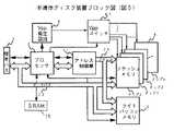
以下に、本発明の一実施例を図を用いて詳細に説明する。図1は、フラッシュメモリを用いた半導体ディスク装置のブロック図である。図中1は、パーソナルコンピュータなどの標準バスであり、このバスを介してシステムからのコマンドやデータの授受を行う。前記バスはこの他にもSCSIインタフェースやシステムのローカルバスなど、補助記憶装置を必要とするシステムとのプロトコルの取決めが有るものであれば特に限定はない。4は複数個のフラッシュメモリ。5は標準バス1から転送されたデータを一時保持するためのライトバッファメモリである。フラッシュメモリは読み出しに比較して書き込みが遅いため、標準バス1から転送されてくる書き込みデータを一時保持し、システム側にバス権を早く開放する。ライトバッファメモリ5は、図中ではスタティックRAMで構成している。しかし、スタティックRAMに限らず、揮発性・不揮発性に関係なくフラッシュメモリ4より高速に書き込みが可能な記憶素子であれば良い。また、半導体ディスク装置内に限らずシステム側にあるデータ記憶領域の一部を用いても良い。ライトバッファメモリ5は標準的なディスクのセクタ容量である512バイト単位で、複数セクタの容量を有する。2はプロセッサである。このプロセッサ2は、ライトバッファメモリ5からフラッシュメモリ4へのデータの書き込みの制御や、標準バスからのコマンドやステータスの授受や解析を行う。11は、システムが管理するセクタ番号である論理セクタ番号を、フラッシュメモリへの書き込む領域のセクタ番号である物理セクタ番号に変換する変換テーブル(始めてアクセスされる論理セクタ番号については、プロセッサ2が変換テーブルを作成する)を記憶しているスタティックラム(SRAM)である。31はフラッシュメモリ4やライトバッファメモリ5の実際のアドレスである物理アドレスを発生するアドレス制御部であり、プロセッサ2によって制御される。6はフラッシュメモリの書き込み電源であるVppを発生するVpp発生回路であり、プロセッサ2で電源発生を制御される。71はフラッシュメモリ4やライトバッファメモリ5のメモリアドレスバスであり、アドレス制御部31より出力される。72はデータバスである。
【0012】
図1の構成の半導体ディスク装置において、プロセッサ2が制御する書き込み動作を図2のフローチャートに示す。標準バス1から書き込みの要求かどうかを判断し(21)、要求がきたとき、プロセッサ2はVpp発生回路6に対して書き込み電源Vppの発生を起動する(22)。そして、プロセッサ2は標準バス1から渡された、システムが管理するセクタ番号である論理セクタ番号を、フラッシュメモリへの書き込む領域のセクタ番号である物理セクタ番号に変換する(23)。この際、標準バス1から転送されてくる複数セクタのデータを、それぞれセクタ単位で書き込むフラッシュメモリが別チップになる様に物理セクタ番号を決定する。例えば、最初に転送されてくる1セクタのデータをフラッシュメモリのチップ0に、次に転送されてくる1セクタのデータをフラッシュメモリのチップ1に、という具合にセクタ単位で割り当てる。この決定した物理セクタ番号を図3の示す書き込み管理テーブルに保持する。この書き込み管理テーブルはアドレス制御部31に存在する。図3では、標準バス1から転送されてくる3セクタ分のデータをライトバッファメモリ5のブロック1からブロック3に保持し、それぞれのブロックの1セクタのデータをそれぞれフラッシュメモリ4のチップ0のセクタ3、チップ1のセクタ2、チップ2のセクタ7へ書き込むことを示している。
【0013】
そして、書き込み管理テーブルの設定が終了したら、標準バス1から転送されてくる3セクタのデータを、書き込み管理テーブルが指定する通りライトバッファメモリ5のブロック1からブロック3の3領域に受け取る。それにより、標準バス1のアクセス権を開放し、フラッシュメモリ4への書き込みを半導体ディスク装置内だけで処理できるようにする(24)。
【0014】
そして、ライトバッファメモリ5に受け取ったデータをフラッシュメモリ4に書き込んでいく。まず、プロセッサ2が書き込み管理テーブルのテーブル番号0を選択することにより、ライトバッファメモリ5やフラッシュメモリ4の物理アドレスがメモリアドレスバス71に出力される。よって、ライトバッファメモリ5のブロック1から1ワードのデータを読み出し(26)、フラッシュメモリ4のチップ0にライトコマンドを書き込み(27)、ライトバッファメモリ5から読み出した1ワードのデータをフラッシュメモリ4のチップ0に書き込む(28)。これで、フラッシュメモリ4のチップ0は内部でのデータの書き込みが開始されるが、内部での書き込みが終了するまでチップ0はデータの読み書きができない。次のチップに書き込むデータがあるか判断し(29)、あるときは、この間に別のメモリチップへの書き込みを行なう。物理セクタへの変換の時述べたように、連続セクタの書き込み時、セクタごとに別のチップに割り当てられている。プロセッサ2が書き込み管理テーブルのテーブル番号1を指定して(25)、ライトバッファメモリ5のブロック2から読みだした1ワードのデータをフラッシュメモリ4のチップ1に書き込む(26,27,28)。続けて、テーブル番号2を指定して、ライトバッファメモリ5のブロック3から読みだした1ワードのデータをフラッシュメモリ4のチップ2に書き込む(26,27,28)。
【0015】
フラッシュメモリ4のチップ0、チップ1、チップ2それぞれに1ワードのデータを書き終えたら(29)、最初に書き込んだフラッシュメモリ4のチップ0のステータスポーリングを行ない(33)、フラッシュメモリ4のチップ内部での書き込みが終了したか確認する。この時も書き込みと同様に、プロセッサ2が書き込み管理テーブルのテーブル番号0を指定することによって、フラッシュメモリ4のチップ0のステータスを読みだす。ここでフラッシュメモリ4のチップ0の内部で書き込みが終了していなければステータスポーリングを繰り返す。書き込みが終了していたら、書き込み管理テーブルのテーブル0のカウンタ値をインクリメントする(34)。同様にして、書き込み管理テーブルに次のテーブルがあるか判断し(35)、あるときは、テーブル番号1を指定し、フラッシュメモリ4のチップ0の次にデータの書き込みを行なったチップ1のステータスポーリングを行なう。そして、フラッシュメモリ4のチップ1の内部での書き込みが終了していたら、その次にデータを書き込んだフラッシュメモリ4のチップ2のステータスポーリングを行なう(33)。書き込みを行なったフラッシュメモリ4のすべてのチップが、内部での書き込みを終了していたら、書き込みシーケンスの最初に戻る。
【0016】
ここで、カウンタが512バイトに達しているか判断し、達していたら、バッファメモリ5からフラッシュメモリ4への全てのデータの書き込みが終了したことになる。カウンタがまだ512バイト以下の場合、前記の書き込み方式で続けて512バイトの書き込みが終了するまで繰り返す。そして、ライトバッファメモリ5からフラッシュメモリ4への全てのデータの書き込みが終了したら、プロセッサ2はVpp発生回路6に対して書き込み電源Vppの発生を停止させる(37)。
【0017】
前記実施例でも明らかな様に3セクタのデータをほぼ1セクタの書き込み時間でフラッシュメモリへの書き込みが行なえる。本実施例では3セクタの書き込みの例を示したが、これは、3セクタより多くのセクタのデータの書き込みも同様であることは明らかである。
【0018】
また前記実施例は、セクタ単位で書き込むフラッシュメモリを別チップに割り当てたが、セクタ内の512バイトを複数のブロックに分割する方法も有る。その分割したブロック単位で異なるフラッシュメモリに書き込みを割り当てる。例えば512バイトを32バイト単位として16ブロックに分割する。そして、1ブロックから16ブロックを、それぞれフラッシュメモリの異なるチップに書き込む。これは32バイト単位としたが、16バイトや64バイトなど任意のバイト単位で良い。
【0019】
また、前記実施例はライトコマンドと1ワードのデータを書き込んでから、次の1ワードのデータの書き込みまで一定の待ち時間があるフラッシュメモリを示した。しかし、ページ書き込みのできるフラッシュメモリ、即ちページライトコマンドを書き込んでから、複数ワードのデータを連続に書き込むことができ、複数ワードのデータを書き込んでからフラッシュメモリ内部でメモリチップへの書き込みが終了するまでに一定の待ち時間があるフラッシュメモリも、前記実施例と同様にして、ページ単位でデータを書き込んでからステータスポーリングまでの時間に、データを書き込んだフラッシュメモリチップとは別のフラッシュメモリチップへのデータの書き込みを行なう。
【0020】
また、フラッシュメモリ4へのデータの書き込みだけでなく、消去についても同様のことがいえる。フラッシュメモリ4はチップ単位あるいは複数ワードを一単位としたブロック単位で消去する。その消去方法は、フラッシュメモリ4に消去するブロックを示すアドレスの指定と同時に消去コマンドを書き込むことで、フラッシュメモリ4内部での消去処理を起動する。そして、フラッシュメモリ4内部での消去が終了するまで一定時間の待ち時間となる。その間は消去処理を行なっているフラッシュメモリ4へはステータスポーリング以外のアクセスはできない。そして、一定時間が経った後ステータスポーリングにより内部での消去の終了が確認されたら、次のフラッシュメモリの消去に移る。この一定時間の間に、消去を実行しているフラッシュメモリとは別のフラッシュメモリに消去コマンドを書き込み、複数のフラッシュメモリの消去を同時に行なうことにより、半導体ディスク装置全体での消去の高速化を実現する。
【0021】
図1の構成の半導体ディスク装置において、プロセッサ2が制御する消去動作を図4のフローチャートに示す。フラッシュメモリ4の消去時にも書き込み電源Vppを印加する必要が有るため、プロセッサ2はVpp発生回路6に対して書き込み電源Vppの発生を起動する(41)。そして、プロセッサ2は消去するフラッシュメモリ4の物理セクタ番号を図3の書き込み管理テーブルに設定する(42)。この時、消去する領域が別のメモリチップになるように設定する。本実施例ではフラッシュメモリ4の消去単位が1セクタである場合について述べる。書き込み管理テーブルに消去するセクタの設定を行なった後、書き込み管理テーブルの指定を更新しながら(43)、テーブルの差し示すフラッシュメモリ4のそれぞれのチップに消去コマンドを書き込む(44)。次消去領域があるか判断し(45)、消去コマンドの書き込みがすべて終了したら、テーブル指定を更新し(46)、最初に消去コマンドを書き込んだメモリチップからステータスポーリングを行ない(47)、フラッシュメモリ4内部での消去処理が終了したかを確認する。そして次テーブル指定の有無を判断し(48)、全てのフラッシュメモリの消去処理が終了したら、プロセッサ2はVpp発生回路6に対して書き込み電源Vppの発生を停止させる(49)。
【0022】
上記実施例は、1セクタ単位での消去を行なうフラッシュメモリについて述べた。しかし、フラッシュメモリによって、消去単位が違う。よって、フラッシュメモリの消去単位の違いにより書き込み管理テーブルの設定方法を違える。フラッシュメモリがチップ単位での消去の場合、書き込み管理テーブルのフラッシュメモリのチップ番号の欄だけの設定で良い。また、複数ワード単位で消去を行なうフラッシュメモリの場合は、書き込み管理テーブルのフラッシュメモリのチップ番号とセクタ番号の2つの欄のセットとなる。しかし、複数ワード単位で消去を行なうフラッシュメモリであっても、1セクタ単位での消去とは限らない。フラッシュメモリが複数セクタの容量を1ブロックとして消去する場合、書き込み管理テーブルのフラッシュメモリのセクタ番号の欄の設定を行なうことで複数セクタの消去となる。
【0023】
前記実施例では、書き込みや消去時など書き込み電源Vppが必要な場合、全てのフラッシュメモリ4に書き込み電源Vppを印加している。しかし、書き込み電源Vppを書き込みを行なうフラッシュメモリにのみ印加する方法も有る。その実施例である半導体ディスク装置のブロック図を図5に示す。図中61はVpp発生回路6からフラッシュメモリ4へ書き込み電源Vppの印加をオンオフするスイッチ部であり、プロセッサ2で制御され、複数の書き込み電源Vppの出力の選択が可能である。その他は図1と同じ構成である。標準バス1から書き込みの要求がきたとき、プロセッサ2はVpp発生回路6に対して書き込み電源Vppの発生を起動する。その後、論理セクタ番号を物理セクタ番号に変換し、物理セクタ番号を図2の書き込み管理テーブルに保持する。この時、書き込みを行なう複数あるいは一つのフラッシュメモリ4への書き込み電源Vppを、Vppスイッチ部61の指定によってそれぞれ印加してやる。この書き込み電源VppのVppスイッチ部61の指定による印加は、書き込み時だけでなく、消去などフラッシュメモリ4が書き込み電源Vppを必要とする場合に行なうのは明らかである。
【0024】
また、前記実施例は、書き込みや消去時に電源電圧とは異なる電圧値の書き込み電源Vppが必要であるフラッシュメモリについて述べた。しかし、単一電源のフラッシュメモリ、要するに書き込み電源Vppが必要の無いフラッシュメモリを搭載した半導体ディスク装置のブロック図を図6に示す。構成は図1と同じであるが、Vpp発生回路6を搭載する必要が無い。また、図2の書き込みフローチャートや、図4の消去のフローチャートで書き込み電源のオンオフ処理が必要無くなるのは明らかである。
【0025】
また、前記実施例では、書き込むフラッシュメモリのチップの選択をチップイネーブル信号CEで行なっている。しかし、チップイネーブル信号CEでなくライトイネーブル信号WEで書き込むフラッシュメモリの選択を制御する方法が有る。その時の半導体ディスク措置のブロック図を図7に示す。図中32は書き込みを行なうフラッシュメモリ4へのライトイネーブル信号WEを選択的にフラッシュメモリ4に与える、WE選択部である。その他は図1と同じ構成である。WE選択部32は書き込みが発生したフラッシュメモリに対してのみライトイネーブル信号を有効にする。プロセッサ2が行なう書き込みの制御は、図2のフローチャートが示す動作と同じとなる。
【0026】
また、フラッシュメモリ4にはライトイネーブル信号WEが無いものが有る。このフラッシュメモリにデータを書き込む場合には、チップイネーブル信号CEと、書き込み電源Vppの制御により書き込みを制御する。このようなフラッシュメモリであっても、本発明を用い、書き込みや消去の高速化が図れる。
【0027】
以上の説明から明らかなように、本発明によれば、大量の書き込みデータが有る補助記憶装置等に、読み出しに比較して書き込みが低速なフラッシュメモリを用いても、装置全体での書き込みを高速に行なえるという効果が有る。特に、連続した大量のデータの書き込みが有る場合に効果が大きい。また、複数領域同時の消去に関しても高速に消去できる。
【0028】
【発明の効果】
本発明は、以上のように構成されているために、データの書き込み時間を短縮した半導体記憶装置を提供できる。
【図面の簡単な説明】
【図1】本発明の動作を行なう一実施例の半導体ディスク装置のブロック図。
【図2】本発明の書き込み動作を示すフローチャート。
【図3】本発明の動作で用いる、書き込み管理テーブル。
【図4】本発明の消去動作を示すフローチャート。
【図5】本発明の動作を行なう一実施例の半導体ディスク装置のブロック図。
【図6】本発明の動作を行なう一実施例の半導体ディスク装置のブロック図。
【図7】本発明の動作を行なう一実施例の半導体ディスク装置のブロック図。
【図8】フラッシュメモリの1ワードの書き込みタイミング波形の説明図。
【符号の説明】
1・・・標準バス
2・・・プロセッサ
31・・・アドレス制御部
32・・・WE選択部
4・・・フラッシュメモリ
5・・・ライトバッファメモリ
6・・・Vpp発生回路
61・・・Vppスイッチ部
71・・・アドレスバス
72・・・データバス[0001]
[Industrial application fields]
The present invention relates to a semiconductor memory device using a flash memory, and more particularly to writing data continuously in a semiconductor disk device using a flash memory.
[0002]
[Prior art]
In the present invention, for example, a plurality of flash EEPROMs that can be read and written in units of words with a plurality of bits as one word and that can be electrically erased in units of chips or in units of a plurality of words are mounted. 1 word of data is written into an arbitrary flash memory mounted on the writing device, and the flash memory in which the writing has been performed can write the next 1 word of data for a certain period of time. In the meantime, one word of data is written in a flash memory different from the flash memory in which writing is performed, which is mounted on the device.
[0003]
FIG. 8 shows timing waveforms for data writing in a flash memory in which writing and erasing are performed using the command control method according to the prior art. In the figure, Vcc is a power supply voltage of the flash memory, and +5 V is always applied. Vpp is a write power supply, and a potential higher than the power supply voltage Vcc is applied when data is written to the flash memory. The address designates a data write area of the flash memory in units of bytes. OE is an output enable signal, which is set to Low when reading data from the flash memory, and set to High at other times. CE is a chip enable signal, and is set to Low when reading and writing commands and data to the flash memory. The CE of this flash memory also serves as a write enable signal. When Vpp is at a high potential and OE is High, data is written at the rising edge of OE. I / O7 and I / O0 to I / O6 are data lines. Next, an operation when writing 1-byte data in the flash memory is shown. First, the command on the data line is written to the flash memory at the rising edge of CE. This command is a write setup command for notifying the flash memory of the start of writing one word of data. After writing this command, the data on the data line is written to the flash memory at the rising edge of CE. The CE Low period when writing this command and data is a minimum of 50 nanoseconds. However, actually, writing to the memory chip has started inside the flash memory, and the next data cannot be written until the internal writing is completed. Here, several tens of microseconds are required until the writing in the flash memory is completed, and a considerable time is required as compared with the writing time of the command and one word of data. Then, status polling is available as means for checking that the writing in the flash memory chip has been completed after the time of several tens of microseconds. This sets CE and OE to Low and reads the status from the I /
[0004]
[Problems to be solved by the invention]
The above technique requires a considerable amount of time when writing a plurality of words of data continuously. Writing commands and data of one word takes several tens of nanoseconds to several hundred nanoseconds. However, a time of several microseconds to several tens of microseconds is required from the writing of one word data to the completion of the writing in the flash memory chip, and the flash memory cannot be accessed during this time. Therefore, the total time for writing one word of data is considerably slower than the reading time. In addition, when data of a plurality of words is written continuously, the writing time increases in proportion to the number of words to be written. For example, when a semiconductor disk device is constructed using a flash memory, data of several kilowords to several tens of kilowords or more is continuously written. Then, since the writing time increases in proportion to the data to be written, the transfer of writing is delayed as a whole system.
[0005]
An object of the present invention is to provide a semiconductor memory device in which a data writing time is shortened.
[0006]
[Means for Solving the Problems]
The present invention
A plurality of nonvolatile semiconductor memories that write data in page units and erase data in block units;
A control unit that controls writing of the data and erasing of the data by each nonvolatile semiconductor memory;
With
In response to one write command from the system, the control unit distributes data for a plurality of sectors associated with one write command from the system to each nonvolatile semiconductor memory in units of sectors. The physical address of each nonvolatile semiconductor memory is generated from the logical sector number managed by the system,
Wherein,oneof said plurality of non-volatile semiconductormemory,while writing the data ofonepageof the distributed data foroneof said plurality of non-volatile semiconductormemory,said plurality ofIt applied to one write command other of said plurality of non-volatile semiconductor memory for data and data of theone page ofonepageof data distributed toanother foroneof the non-volatile semiconductor memory,
The control unit generates an address of a block of each nonvolatile semiconductor memory so that an area to be erased is distributed to the plurality of nonvolatile semiconductor memories in the block unit,
Wherein, during said one of the plurality of non-volatile semiconductor memory is running erasure of the data,inadditiontotheoneof the plurality of non-volatile semiconductormemory,for executing the erasure of the data Give erase command,
The control unit performs status polling of the plurality of nonvolatile semiconductor memories after giving the erase command to the plurality of nonvolatile semiconductor memories.
A semiconductor memory device is provided.
[0007]
[Action]
According to the semiconductor memory device according to the present invention, the data betweenone of saidplurality of non-volatile semiconductor memoryis running the data erasure, the processor,the other one ofsaid plurality of non-volatile semiconductor memory writing thecommand for executing the erasing.In addition, the processor includes the plurality of nonvolatile semiconductors in the order in which the command for executing the data erasure is written after the writing of the command for executing the data erasing to the plurality of nonvolatile semiconductor memories is completed. Performs memory status polling.
[0008]
【Example】
In this embodiment, in the case of continuous data writing, control is performed so that data is not continuously written in the same flash memory but is written in another flash memory.
[0009]
There is a waiting time of several microseconds to several tens of microseconds from writing one word of data to the flash memory until writing the next data. Therefore, when there is continuous write data, one word of data is continuously written to another flash memory during this waiting time. Then, when the waiting time of the first written flash memory has passed, status polling is performed from the first flash memory, and the next one word of data is written. In this manner, writing to another flash memory is performed during the waiting time of the flash memory.
[0010]
When the flash memory is used for writing a plurality of continuous data, according to the present embodiment, low-speed writing of the flash memory can be speeded up in total for the apparatus. That is, when a flash memory is used for a semiconductor disk device, a plurality of continuous data is written. However, in the case of continuous data writing, writing to the flash memory is slower than reading, so the total transfer rate is reduced. However, according to the present embodiment, the writing speed of the entire apparatus can be increased even when the writing speed of the flash memory is low.
[0011]
Hereinafter, an embodiment of the present invention will be described in detail with reference to the drawings. FIG. 1 is a block diagram of a semiconductor disk device using a flash memory. In the figure,
[0012]
The write operation controlled by the
[0013]
When the setting of the write management table is completed, the data of 3 sectors transferred from the
[0014]
Then, the data received in the write buffer memory 5 is written into the flash memory 4. First, when the
[0015]
After writing one word of data to each of
[0016]
Here, it is determined whether the counter has reached 512 bytes. If it has reached, writing of all data from the buffer memory 5 to the flash memory 4 has been completed. If the counter is still 512 bytes or less, the above writing method is repeated until 512 bytes have been written. When the writing of all data from the write buffer memory 5 to the flash memory 4 is completed, the
[0017]
As is apparent from the above embodiment, data of 3 sectors can be written to the flash memory in approximately 1 sector of writing time. In this embodiment, an example of writing in three sectors is shown, but it is obvious that writing data in more sectors than three sectors is the same.
[0018]
In the above embodiment, the flash memory to be written on a sector basis is allocated to another chip, but there is a method of dividing 512 bytes in a sector into a plurality of blocks. Writes are assigned to different flash memories in units of the divided blocks. For example, 512 bytes are divided into 16 blocks in units of 32 bytes. Then, 1 to 16 blocks are written to different chips of the flash memory. This is a 32-byte unit, but it may be an arbitrary byte unit such as 16 bytes or 64 bytes.
[0019]
In the above embodiment, the flash memory has a certain waiting time from the writing of the write command and one word of data to the writing of the next one word of data. However, a flash memory capable of page writing, that is, a plurality of words of data can be continuously written after a page write command is written, and writing to the memory chip inside the flash memory is completed after the writing of the plurality of words of data. In the same way as in the above embodiment, the flash memory having a certain waiting time until the status polling is performed on a flash memory chip different from the flash memory chip on which the data is written. Write data.
[0020]
The same applies to erasure as well as data writing to the flash memory 4. The flash memory 4 is erased in units of chips or in units of blocks each having a plurality of words as one unit. The erasing method starts erasing processing in the flash memory 4 by writing an erasing command simultaneously with designating an address indicating a block to be erased in the flash memory 4. Then, there is a waiting time of a certain time until erasing in the flash memory 4 is completed. In the meantime, access other than status polling cannot be performed on the flash memory 4 performing the erasure process. When the end of internal erasure is confirmed by status polling after a predetermined time has passed, the process proceeds to erasure of the next flash memory. During this fixed period of time, the erase command is written to a flash memory different from the flash memory that is erasing, and multiple flash memories are erased at the same time, thereby speeding up erasure of the entire semiconductor disk device. Realize.
[0021]
The erase operation controlled by the
[0022]
In the above embodiment, the flash memory that performs erasing in units of one sector has been described. However, the erase unit differs depending on the flash memory. Therefore, the setting method of the write management table differs depending on the erase unit of the flash memory. When the flash memory is erased in units of chips, it is sufficient to set only the chip number column of the flash memory in the write management table. Further, in the case of a flash memory that performs erasing in units of a plurality of words, it becomes a set of two columns of the flash memory chip number and sector number of the write management table. However, even a flash memory that erases in units of multiple words is not necessarily erased in units of one sector. When the flash memory erases the capacity of a plurality of sectors as one block, a plurality of sectors are erased by setting the flash memory sector number column in the write management table.
[0023]
In the above embodiment, when the write power supply Vpp is necessary for writing and erasing, the write power supply Vpp is applied to all the flash memories 4. However, there is a method in which the write power supply Vpp is applied only to the flash memory for writing. FIG. 5 shows a block diagram of a semiconductor disk device according to the embodiment. In the figure, reference numeral 61 denotes a switch unit for turning on / off the application of the write power supply Vpp from the
[0024]
In the above embodiment, the flash memory is described which requires the write power supply Vpp having a voltage value different from the power supply voltage at the time of writing or erasing. However, FIG. 6 shows a block diagram of a semiconductor disk device equipped with a flash memory having a single power source, that is, a flash memory that does not require a write power source Vpp. The configuration is the same as in FIG. 1, but it is not necessary to mount the
[0025]
In the above embodiment, the chip of the flash memory to be written is selected by the chip enable signal CE. However, there is a method for controlling selection of a flash memory to be written by the write enable signal WE instead of the chip enable signal CE. FIG. 7 shows a block diagram of the semiconductor disk measures at that time. In the figure, reference numeral 32 denotes a WE selection unit that selectively supplies the flash memory 4 with a write enable signal WE for writing to the flash memory 4. The rest of the configuration is the same as in FIG. The WE selection unit 32 validates the write enable signal only for the flash memory in which writing has occurred. The write control performed by the
[0026]
Some flash memories 4 do not have a write enable signal WE. When writing data to the flash memory, the writing is controlled by controlling the chip enable signal CE and the write power supply Vpp. Even in such a flash memory, the present invention can be used to speed up writing and erasing.
[0027]
As can be seen from the above description, according to the present invention, even if an auxiliary storage device having a large amount of write data uses a flash memory that is slower in writing than read, the entire device can be written at high speed. There is an effect that can be done. In particular, the effect is great when there is continuous writing of a large amount of data. Further, it is possible to erase at a high speed with respect to simultaneous erasure of a plurality of areas.
[0028]
【The invention's effect】
Since the present invention is configured as described above, it is possible to provide a semiconductor memory device in which the data writing time is shortened.
[Brief description of the drawings]
FIG. 1 is a block diagram of a semiconductor disk device according to an embodiment for performing the operation of the present invention.
FIG. 2 is a flowchart showing a write operation of the present invention.
FIG. 3 is a write management table used in the operation of the present invention.
FIG. 4 is a flowchart showing an erase operation of the present invention.
FIG. 5 is a block diagram of a semiconductor disk device according to an embodiment for performing the operation of the present invention.
FIG. 6 is a block diagram of a semiconductor disk device according to an embodiment for performing the operation of the present invention.
FIG. 7 is a block diagram of a semiconductor disk device according to an embodiment for performing the operation of the present invention.
FIG. 8 is an explanatory diagram of a write timing waveform of one word in a flash memory.
[Explanation of symbols]
DESCRIPTION OF
Claims (5)
Translated fromJapanese各不揮発性半導体メモリによる前記データの書き込みと前記データの消去とを制御する制御部と、
を備え、
前記制御部は、システムからの1つの書き込みコマンドに応答して、前記システムからの1つの書き込みコマンドに伴う複数セクタ分のデータがセクタ単位で前記各不揮発性半導体メモリに分配されるように、テーブルを参照して、前記システムが管理する論理セクタ番号から前記各不揮発性半導体メモリの物理アドレスを発生し、
前記制御部は、前記複数の不揮発性半導体メモリの1つが、前記複数の不揮発性半導体メモリの1つのために分配されたデータのうちの1ページ分のデータを書き込んでいる間に、前記複数の不揮発性半導体メモリの他の1つのために分配されたデータのうちの1ページ分のデータ及び当該1ページ分のデータのための書き込みコマンドを前記複数の不揮発性半導体メモリの他の1つに与え、
前記制御部は、消去すべき領域が前記ブロック単位で前記複数の不揮発性半導体メモリに分配されるように、前記各不揮発性半導体メモリのブロックのアドレスを発生し、
前記制御部は、前記複数の不揮発性半導体メモリの1つが前記データの消去を実行している間に、前記複数の不揮発性半導体メモリの他の1つに、前記データの消去を実行させるための消去コマンドを与え、
前記制御部は、前記複数の不揮発性半導体メモリへ前記消去コマンドを与えた後に、前記複数の不揮発性半導体メモリのステータスポーリングを行う、
ことを特徴とする半導体記憶装置。A plurality of nonvolatile semiconductor memories that write data inpage units and erase data in block units;
A control unit that controls writing of the data and erasing of the data by each nonvolatile semiconductor memory;
With
The control unit, in response to one write command from the system, such that a plurality of sectors of data associated with one write command from the system is distributed to the each non-volatile semiconductor memory on a sector basis,the table see,it generates the physicaladdresses of the respective non-volatile semiconductor memoryfrom the logical sector number which the systemmanages,
Thecontrol unit , while one of the plurality of nonvolatile semiconductor memories is writing data foronepage ofdata distributed for one of the plurality of nonvolatile semiconductor memories,Onepage ofdata distributed for another one of the nonvolatile semiconductor memories and a write command for theone page of data are given to the other one of the plurality of nonvolatile semiconductor memories. ,
Thecontrol unitgenerates an address of ablock of each nonvolatile semiconductor memory so that an area to be erased is distributed to the plurality of nonvolatile semiconductor memories in the block unit,
Wherein, during said one of the plurality of non-volatile semiconductor memory is running erasure of thedata, in addition to the one of the plurality of non-volatile semiconductor memory, for executing the erasure of the data Give erase command,
Wherein, after giving the erase command to the plurality of non-volatile semiconductormemory, performs status polling of the plurality of non-volatile semiconductor memory,
A semiconductor memory device.
前記各不揮発性半導体メモリは、1つのフラッシュメモリチップで構成される、
ことを特徴とする半導体記憶装置。The semiconductor memory device according to claim 1,
Each nonvolatile semiconductor memory is composed of one flash memory chip.
A semiconductor memory device.
前記各不揮発性半導体メモリは、前記データ消去の実行中、ステータスポーリング以外のアクセスを受け付けない、
ことを特徴とする半導体記憶装置。The semiconductor memory device according to claim 1,
Each nonvolatile semiconductor memory does not accept access other than status polling during execution of the data erasure,
A semiconductor memory device.
前記制御部は、前記ステータスポーリングにより前記データ消去が終了したことを確認した場合に、前記データ消去が終了した不揮発性半導体メモリに、前記消去コマンドを新たに書き込む、
ことを特徴とする半導体記憶装置。The semiconductor memory device according to claim 1, wherein
When thecontrol unit confirms that the data erasure is completed by the status polling, thecontrol unit newly writes the erasure command to the nonvolatile semiconductor memory in which the data erasure is completed.
A semiconductor memory device.
バッファメモリをさらに備え、
前記1セクタは、512バイトを含み、
前記制御部は、前記バッファメモリを介して、前記システムからのデータを前記複数の不揮発性半導体メモリへ書き込む、
ことを特徴とする半導体記憶装置。The semiconductor memory device accordingto any one of claims 1, 2, 3, and 4 ,
A buffer memory,
The one sector includes 512 bytes,
Thecontrol unit writes data from the system to the plurality of nonvolatile semiconductor memories via the buffer memory.
A semiconductor memory device.
Priority Applications (1)
| Application Number | Priority Date | Filing Date | Title |
|---|---|---|---|
| JP2002011910AJP3793464B2 (en) | 2002-01-21 | 2002-01-21 | Semiconductor memory device |
Applications Claiming Priority (1)
| Application Number | Priority Date | Filing Date | Title |
|---|---|---|---|
| JP2002011910AJP3793464B2 (en) | 2002-01-21 | 2002-01-21 | Semiconductor memory device |
Related Parent Applications (1)
| Application Number | Title | Priority Date | Filing Date |
|---|---|---|---|
| JP16307492ADivisionJP3328321B2 (en) | 1992-06-22 | 1992-06-22 | Semiconductor storage device |
Related Child Applications (3)
| Application Number | Title | Priority Date | Filing Date |
|---|---|---|---|
| JP2004116930ADivisionJP3793540B2 (en) | 2004-04-12 | 2004-04-12 | Semiconductor memory device |
| JP2004379652ADivisionJP3793542B2 (en) | 2004-12-28 | 2004-12-28 | Semiconductor memory device |
| JP2005229415ADivisionJP4158934B2 (en) | 2005-08-08 | 2005-08-08 | Semiconductor storage medium |
Publications (2)
| Publication Number | Publication Date |
|---|---|
| JP2002236612A JP2002236612A (en) | 2002-08-23 |
| JP3793464B2true JP3793464B2 (en) | 2006-07-05 |
Family
ID=19191706
Family Applications (1)
| Application Number | Title | Priority Date | Filing Date |
|---|---|---|---|
| JP2002011910AExpired - LifetimeJP3793464B2 (en) | 2002-01-21 | 2002-01-21 | Semiconductor memory device |
Country Status (1)
| Country | Link |
|---|---|
| JP (1) | JP3793464B2 (en) |
Families Citing this family (1)
| Publication number | Priority date | Publication date | Assignee | Title |
|---|---|---|---|---|
| KR100628832B1 (en) | 2004-11-10 | 2006-09-26 | 삼성전자주식회사 | Pumping voltage generation circuit of nonvolatile semiconductor memory device |
Family Cites Families (15)
| Publication number | Priority date | Publication date | Assignee | Title |
|---|---|---|---|---|
| JPS63124298A (en)* | 1986-11-13 | 1988-05-27 | Matsushita Graphic Commun Syst Inc | Memory device |
| JPS63288384A (en)* | 1987-05-20 | 1988-11-25 | Matsushita Electric Ind Co Ltd | memory card |
| JP2750704B2 (en)* | 1988-08-29 | 1998-05-13 | 日立マクセル株式会社 | Information writing method of IC card and IC card |
| JPH02114313A (en)* | 1988-10-24 | 1990-04-26 | Advantest Corp | High speed external storage device |
| JP2654596B2 (en)* | 1989-02-06 | 1997-09-17 | 株式会社日立製作所 | Non-volatile storage device |
| EP0935255A2 (en)* | 1989-04-13 | 1999-08-11 | SanDisk Corporation | Flash EEPROM system |
| JPH02304614A (en)* | 1989-05-19 | 1990-12-18 | Nippon Telegr & Teleph Corp <Ntt> | Peripheral equipment access system |
| JPH03252993A (en)* | 1990-03-01 | 1991-11-12 | Fuji Electric Co Ltd | E↑2PROM information writing device |
| JPH0433029A (en)* | 1990-05-24 | 1992-02-04 | Matsushita Electric Ind Co Ltd | Memory devices and their driving methods |
| JPH0457295A (en)* | 1990-06-22 | 1992-02-25 | Nec Corp | Electrically writable/erasable memory circuit |
| JPH0484216A (en)* | 1990-07-26 | 1992-03-17 | Toshiba Corp | Data erasing method for semiconductor disk device |
| JP2582487B2 (en)* | 1991-07-12 | 1997-02-19 | インターナショナル・ビジネス・マシーンズ・コーポレイション | External storage system using semiconductor memory and control method thereof |
| US5263003A (en)* | 1991-11-12 | 1993-11-16 | Allen-Bradley Company, Inc. | Flash memory circuit and method of operation |
| JPH05242688A (en)* | 1992-02-27 | 1993-09-21 | Hitachi Ltd | Recording and reproducing device employing flash eeprom |
| JPH05324000A (en)* | 1992-05-15 | 1993-12-07 | Sharp Corp | Audio recorder using semiconductor memory |
- 2002
- 2002-01-21JPJP2002011910Apatent/JP3793464B2/ennot_activeExpired - Lifetime
Also Published As
| Publication number | Publication date |
|---|---|
| JP2002236612A (en) | 2002-08-23 |
Similar Documents
| Publication | Publication Date | Title |
|---|---|---|
| JP3328321B2 (en) | Semiconductor storage device | |
| US8001319B2 (en) | Semiconductor storage device | |
| KR100716576B1 (en) | Memory card, logical address assignment method and data recording method | |
| JP4406339B2 (en) | Controller, memory card and control method thereof | |
| US5920884A (en) | Nonvolatile memory interface protocol which selects a memory device, transmits an address, deselects the device, subsequently reselects the device and accesses data | |
| JP2000067574A (en) | Semiconductor storage device | |
| JP4034971B2 (en) | Memory controller and memory system device | |
| US12423251B2 (en) | Memory device, method for controlling memory device and memory system | |
| JP4382131B2 (en) | Semiconductor disk device | |
| JP3793542B2 (en) | Semiconductor memory device | |
| JP3793464B2 (en) | Semiconductor memory device | |
| JP3328605B2 (en) | Semiconductor storage device | |
| JP3793540B2 (en) | Semiconductor memory device | |
| JP4158934B2 (en) | Semiconductor storage medium | |
| JP3328604B2 (en) | Semiconductor storage device | |
| JP2023044471A (en) | Memory system and memory control method | |
| JP7031672B2 (en) | Memory controller, memory system and information processing system | |
| JP2021152779A (en) | Semiconductor memory device | |
| KR20210012818A (en) | Memory device and operating method thereof | |
| JP2006215595A (en) | Storage | |
| JP2004213695A (en) | Nonvolatile memory, memory card using it, information processor and software write protection control method for nonvolatile memory | |
| KR20060012139A (en) | Flash memory control method | |
| JP2004303277A (en) | Nonvolatile memory, memory card and information processor using the same, and software write protect control method for nonvolatile memory |
Legal Events
| Date | Code | Title | Description |
|---|---|---|---|
| A131 | Notification of reasons for refusal | Free format text:JAPANESE INTERMEDIATE CODE: A131 Effective date:20040210 | |
| A521 | Written amendment | Free format text:JAPANESE INTERMEDIATE CODE: A523 Effective date:20040412 | |
| RD02 | Notification of acceptance of power of attorney | Free format text:JAPANESE INTERMEDIATE CODE: A7422 Effective date:20040412 | |
| A02 | Decision of refusal | Free format text:JAPANESE INTERMEDIATE CODE: A02 Effective date:20041102 | |
| A521 | Written amendment | Free format text:JAPANESE INTERMEDIATE CODE: A523 Effective date:20041228 | |
| A521 | Written amendment | Free format text:JAPANESE INTERMEDIATE CODE: A523 Effective date:20050201 | |
| A911 | Transfer to examiner for re-examination before appeal (zenchi) | Free format text:JAPANESE INTERMEDIATE CODE: A911 Effective date:20050207 | |
| A131 | Notification of reasons for refusal | Free format text:JAPANESE INTERMEDIATE CODE: A131 Effective date:20050607 | |
| A521 | Written amendment | Free format text:JAPANESE INTERMEDIATE CODE: A523 Effective date:20050808 | |
| TRDD | Decision of grant or rejection written | ||
| A01 | Written decision to grant a patent or to grant a registration (utility model) | Free format text:JAPANESE INTERMEDIATE CODE: A01 Effective date:20060404 | |
| A61 | First payment of annual fees (during grant procedure) | Free format text:JAPANESE INTERMEDIATE CODE: A61 Effective date:20060407 | |
| FPAY | Renewal fee payment (event date is renewal date of database) | Free format text:PAYMENT UNTIL: 20090414 Year of fee payment:3 | |
| S111 | Request for change of ownership or part of ownership | Free format text:JAPANESE INTERMEDIATE CODE: R313113 | |
| FPAY | Renewal fee payment (event date is renewal date of database) | Free format text:PAYMENT UNTIL: 20090414 Year of fee payment:3 | |
| R360 | Written notification for declining of transfer of rights | Free format text:JAPANESE INTERMEDIATE CODE: R360 | |
| FPAY | Renewal fee payment (event date is renewal date of database) | Free format text:PAYMENT UNTIL: 20090414 Year of fee payment:3 | |
| R370 | Written measure of declining of transfer procedure | Free format text:JAPANESE INTERMEDIATE CODE: R370 | |
| FPAY | Renewal fee payment (event date is renewal date of database) | Free format text:PAYMENT UNTIL: 20090414 Year of fee payment:3 | |
| S111 | Request for change of ownership or part of ownership | Free format text:JAPANESE INTERMEDIATE CODE: R313113 | |
| FPAY | Renewal fee payment (event date is renewal date of database) | Free format text:PAYMENT UNTIL: 20090414 Year of fee payment:3 | |
| R350 | Written notification of registration of transfer | Free format text:JAPANESE INTERMEDIATE CODE: R350 | |
| FPAY | Renewal fee payment (event date is renewal date of database) | Free format text:PAYMENT UNTIL: 20090414 Year of fee payment:3 | |
| S111 | Request for change of ownership or part of ownership | Free format text:JAPANESE INTERMEDIATE CODE: R313113 | |
| FPAY | Renewal fee payment (event date is renewal date of database) | Free format text:PAYMENT UNTIL: 20090414 Year of fee payment:3 | |
| R350 | Written notification of registration of transfer | Free format text:JAPANESE INTERMEDIATE CODE: R350 | |
| FPAY | Renewal fee payment (event date is renewal date of database) | Free format text:PAYMENT UNTIL: 20100414 Year of fee payment:4 | |
| FPAY | Renewal fee payment (event date is renewal date of database) | Free format text:PAYMENT UNTIL: 20110414 Year of fee payment:5 | |
| FPAY | Renewal fee payment (event date is renewal date of database) | Free format text:PAYMENT UNTIL: 20120414 Year of fee payment:6 | |
| FPAY | Renewal fee payment (event date is renewal date of database) | Free format text:PAYMENT UNTIL: 20120414 Year of fee payment:6 | |
| FPAY | Renewal fee payment (event date is renewal date of database) | Free format text:PAYMENT UNTIL: 20130414 Year of fee payment:7 | |
| EXPY | Cancellation because of completion of term | ||
| FPAY | Renewal fee payment (event date is renewal date of database) | Free format text:PAYMENT UNTIL: 20130414 Year of fee payment:7 |