JP3786427B2 - Method for manufacturing light emitting device - Google Patents
Method for manufacturing light emitting deviceDownload PDFInfo
- Publication number
- JP3786427B2 JP3786427B2JP50681398AJP50681398AJP3786427B2JP 3786427 B2JP3786427 B2JP 3786427B2JP 50681398 AJP50681398 AJP 50681398AJP 50681398 AJP50681398 AJP 50681398AJP 3786427 B2JP3786427 B2JP 3786427B2
- Authority
- JP
- Japan
- Prior art keywords
- light emitting
- electrode
- liquid
- line
- optical material
- Prior art date
- Legal status (The legal status is an assumption and is not a legal conclusion. Google has not performed a legal analysis and makes no representation as to the accuracy of the status listed.)
- Expired - Lifetime
Links
- 238000000034methodMethods0.000titleclaimsdescription46
- 238000004519manufacturing processMethods0.000titleclaimsdescription36
- 239000000463materialSubstances0.000claimsdescription94
- 239000000758substrateSubstances0.000claimsdescription31
- 239000010408filmSubstances0.000description62
- 230000003287optical effectEffects0.000description55
- 239000007788liquidSubstances0.000description51
- 239000010410layerSubstances0.000description41
- 239000011159matrix materialSubstances0.000description28
- 239000004065semiconductorSubstances0.000description21
- 239000010409thin filmSubstances0.000description20
- 238000002347injectionMethods0.000description19
- 239000007924injectionSubstances0.000description19
- 230000008569processEffects0.000description19
- 239000011229interlayerSubstances0.000description16
- 238000000059patterningMethods0.000description16
- 238000009826distributionMethods0.000description12
- 239000012705liquid precursorSubstances0.000description12
- 238000010586diagramMethods0.000description9
- -1phosphorus ionsChemical class0.000description7
- 239000002904solventSubstances0.000description7
- 229910021417amorphous siliconInorganic materials0.000description6
- 239000011248coating agentSubstances0.000description6
- 238000000576coating methodMethods0.000description6
- 238000005530etchingMethods0.000description5
- 238000000926separation methodMethods0.000description5
- BOTDANWDWHJENH-UHFFFAOYSA-NTetraethyl orthosilicateChemical compoundCCO[Si](OCC)(OCC)OCCBOTDANWDWHJENH-UHFFFAOYSA-N0.000description4
- 230000008901benefitEffects0.000description4
- 239000003990capacitorSubstances0.000description4
- 230000000694effectsEffects0.000description4
- 238000010438heat treatmentMethods0.000description4
- 230000001678irradiating effectEffects0.000description4
- 238000003892spreadingMethods0.000description4
- 230000007480spreadingEffects0.000description4
- XLYOFNOQVPJJNP-UHFFFAOYSA-NwaterSubstancesOXLYOFNOQVPJJNP-UHFFFAOYSA-N0.000description4
- VYPSYNLAJGMNEJ-UHFFFAOYSA-NSilicium dioxideChemical compoundO=[Si]=OVYPSYNLAJGMNEJ-UHFFFAOYSA-N0.000description3
- 239000004973liquid crystal related substanceSubstances0.000description3
- 238000005268plasma chemical vapour depositionMethods0.000description3
- 229910021420polycrystalline siliconInorganic materials0.000description3
- 239000002243precursorSubstances0.000description3
- 229910052814silicon oxideInorganic materials0.000description3
- XDTMQSROBMDMFD-UHFFFAOYSA-NCyclohexaneChemical compoundC1CCCCC1XDTMQSROBMDMFD-UHFFFAOYSA-N0.000description2
- MYMOFIZGZYHOMD-UHFFFAOYSA-NDioxygenChemical compoundO=OMYMOFIZGZYHOMD-UHFFFAOYSA-N0.000description2
- 239000004642PolyimideSubstances0.000description2
- HCHKCACWOHOZIP-UHFFFAOYSA-NZincChemical compound[Zn]HCHKCACWOHOZIP-UHFFFAOYSA-N0.000description2
- 230000008859changeEffects0.000description2
- 229910001882dioxygenInorganic materials0.000description2
- 230000005684electric fieldEffects0.000description2
- 239000007789gasSubstances0.000description2
- 238000005224laser annealingMethods0.000description2
- 229910052751metalInorganic materials0.000description2
- 239000002184metalSubstances0.000description2
- 230000004048modificationEffects0.000description2
- 238000012986modificationMethods0.000description2
- 229920000553poly(phenylenevinylene)Polymers0.000description2
- 229920001721polyimidePolymers0.000description2
- 230000001681protective effectEffects0.000description2
- 239000007787solidSubstances0.000description2
- 239000000126substanceSubstances0.000description2
- 229910052725zincInorganic materials0.000description2
- 239000011701zincSubstances0.000description2
- RETDKIXQRINZEF-UHFFFAOYSA-N1,3-benzoxazole;zincChemical compound[Zn].C1=CC=C2OC=NC2=C1RETDKIXQRINZEF-UHFFFAOYSA-N0.000description1
- 229910052693EuropiumInorganic materials0.000description1
- ZOKXTWBITQBERF-UHFFFAOYSA-NMolybdenumChemical compound[Mo]ZOKXTWBITQBERF-UHFFFAOYSA-N0.000description1
- 241001408050OxydiaSpecies0.000description1
- 229920000265PolyparaphenylenePolymers0.000description1
- NRCMAYZCPIVABH-UHFFFAOYSA-NQuinacridoneChemical classN1C2=CC=CC=C2C(=O)C2=C1C=C1C(=O)C3=CC=CC=C3NC1=C2NRCMAYZCPIVABH-UHFFFAOYSA-N0.000description1
- 229910004298SiO 2Inorganic materials0.000description1
- XUIMIQQOPSSXEZ-UHFFFAOYSA-NSiliconChemical compound[Si]XUIMIQQOPSSXEZ-UHFFFAOYSA-N0.000description1
- RTAQQCXQSZGOHL-UHFFFAOYSA-NTitaniumChemical compound[Ti]RTAQQCXQSZGOHL-UHFFFAOYSA-N0.000description1
- DGEZNRSVGBDHLK-UHFFFAOYSA-N[1,10]phenanthrolineChemical compoundC1=CN=C2C3=NC=CC=C3C=CC2=C1DGEZNRSVGBDHLK-UHFFFAOYSA-N0.000description1
- 229910052782aluminiumInorganic materials0.000description1
- XAGFODPZIPBFFR-UHFFFAOYSA-NaluminiumChemical compound[Al]XAGFODPZIPBFFR-UHFFFAOYSA-N0.000description1
- 239000007864aqueous solutionSubstances0.000description1
- 150000004984aromatic diaminesChemical class0.000description1
- 239000003795chemical substances by applicationSubstances0.000description1
- 239000003086colorantSubstances0.000description1
- 238000007796conventional methodMethods0.000description1
- 150000004696coordination complexChemical class0.000description1
- 238000002425crystallisationMethods0.000description1
- 230000008025crystallizationEffects0.000description1
- 239000000539dimerSubstances0.000description1
- 125000005678ethenylene groupChemical group[H]C([*:1])=C([H])[*:2]0.000description1
- OGPBJKLSAFTDLK-UHFFFAOYSA-Neuropium atomChemical compound[Eu]OGPBJKLSAFTDLK-UHFFFAOYSA-N0.000description1
- 239000011521glassSubstances0.000description1
- 230000005484gravityEffects0.000description1
- 239000012535impuritySubstances0.000description1
- 239000011344liquid materialSubstances0.000description1
- 239000006193liquid solutionSubstances0.000description1
- 229910052750molybdenumInorganic materials0.000description1
- 239000011733molybdenumSubstances0.000description1
- 150000004767nitridesChemical class0.000description1
- 230000005693optoelectronicsEffects0.000description1
- VLTRZXGMWDSKGL-UHFFFAOYSA-MperchlorateInorganic materials[O-]Cl(=O)(=O)=OVLTRZXGMWDSKGL-UHFFFAOYSA-M0.000description1
- 229910052698phosphorusInorganic materials0.000description1
- 239000011574phosphorusSubstances0.000description1
- 229920002120photoresistant polymerPolymers0.000description1
- 230000010287polarizationEffects0.000description1
- 229920000642polymerPolymers0.000description1
- 229920005591polysiliconPolymers0.000description1
- 150000004032porphyrinsChemical class0.000description1
- 150000003219pyrazolinesChemical class0.000description1
- LISFMEBWQUVKPJ-UHFFFAOYSA-Nquinolin-2-olChemical compoundC1=CC=C2NC(=O)C=CC2=C1LISFMEBWQUVKPJ-UHFFFAOYSA-N0.000description1
- YYMBJDOZVAITBP-UHFFFAOYSA-NrubreneChemical classC1=CC=CC=C1C(C1=C(C=2C=CC=CC=2)C2=CC=CC=C2C(C=2C=CC=CC=2)=C11)=C(C=CC=C2)C2=C1C1=CC=CC=C1YYMBJDOZVAITBP-UHFFFAOYSA-N0.000description1
- 229910052710siliconInorganic materials0.000description1
- 239000010703siliconSubstances0.000description1
- LIVNPJMFVYWSIS-UHFFFAOYSA-Nsilicon monoxideChemical compound[Si-]#[O+]LIVNPJMFVYWSIS-UHFFFAOYSA-N0.000description1
- 239000007790solid phaseSubstances0.000description1
- 238000007711solidificationMethods0.000description1
- 230000008023solidificationEffects0.000description1
- 239000000243solutionSubstances0.000description1
- 238000004528spin coatingMethods0.000description1
- 230000002269spontaneous effectEffects0.000description1
- 238000004544sputter depositionMethods0.000description1
- 229910052715tantalumInorganic materials0.000description1
- GUVRBAGPIYLISA-UHFFFAOYSA-Ntantalum atomChemical compound[Ta]GUVRBAGPIYLISA-UHFFFAOYSA-N0.000description1
- 229910052719titaniumInorganic materials0.000description1
- 239000010936titaniumSubstances0.000description1
- JFLKFZNIIQFQBS-FNCQTZNRSA-Ntrans,trans-1,4-Diphenyl-1,3-butadieneChemical classC=1C=CC=CC=1\C=C\C=C\C1=CC=CC=C1JFLKFZNIIQFQBS-FNCQTZNRSA-N0.000description1
- 150000003852triazolesChemical class0.000description1
- 125000006617triphenylamine groupChemical group0.000description1
- WFKWXMTUELFFGS-UHFFFAOYSA-NtungstenChemical compound[W]WFKWXMTUELFFGS-UHFFFAOYSA-N0.000description1
- 229910052721tungstenInorganic materials0.000description1
- 239000010937tungstenSubstances0.000description1
Images


Classifications
- G—PHYSICS
- G09—EDUCATION; CRYPTOGRAPHY; DISPLAY; ADVERTISING; SEALS
- G09F—DISPLAYING; ADVERTISING; SIGNS; LABELS OR NAME-PLATES; SEALS
- G09F9/00—Indicating arrangements for variable information in which the information is built-up on a support by selection or combination of individual elements
- G09F9/30—Indicating arrangements for variable information in which the information is built-up on a support by selection or combination of individual elements in which the desired character or characters are formed by combining individual elements
- G—PHYSICS
- G02—OPTICS
- G02F—OPTICAL DEVICES OR ARRANGEMENTS FOR THE CONTROL OF LIGHT BY MODIFICATION OF THE OPTICAL PROPERTIES OF THE MEDIA OF THE ELEMENTS INVOLVED THEREIN; NON-LINEAR OPTICS; FREQUENCY-CHANGING OF LIGHT; OPTICAL LOGIC ELEMENTS; OPTICAL ANALOGUE/DIGITAL CONVERTERS
- G02F1/00—Devices or arrangements for the control of the intensity, colour, phase, polarisation or direction of light arriving from an independent light source, e.g. switching, gating or modulating; Non-linear optics
- G02F1/01—Devices or arrangements for the control of the intensity, colour, phase, polarisation or direction of light arriving from an independent light source, e.g. switching, gating or modulating; Non-linear optics for the control of the intensity, phase, polarisation or colour
- G02F1/13—Devices or arrangements for the control of the intensity, colour, phase, polarisation or direction of light arriving from an independent light source, e.g. switching, gating or modulating; Non-linear optics for the control of the intensity, phase, polarisation or colour based on liquid crystals, e.g. single liquid crystal display cells
- G02F1/133—Constructional arrangements; Operation of liquid crystal cells; Circuit arrangements
- G02F1/1333—Constructional arrangements; Manufacturing methods
- G02F1/133377—Cells with plural compartments or having plurality of liquid crystal microcells partitioned by walls, e.g. one microcell per pixel
- G—PHYSICS
- G02—OPTICS
- G02F—OPTICAL DEVICES OR ARRANGEMENTS FOR THE CONTROL OF LIGHT BY MODIFICATION OF THE OPTICAL PROPERTIES OF THE MEDIA OF THE ELEMENTS INVOLVED THEREIN; NON-LINEAR OPTICS; FREQUENCY-CHANGING OF LIGHT; OPTICAL LOGIC ELEMENTS; OPTICAL ANALOGUE/DIGITAL CONVERTERS
- G02F1/00—Devices or arrangements for the control of the intensity, colour, phase, polarisation or direction of light arriving from an independent light source, e.g. switching, gating or modulating; Non-linear optics
- G02F1/01—Devices or arrangements for the control of the intensity, colour, phase, polarisation or direction of light arriving from an independent light source, e.g. switching, gating or modulating; Non-linear optics for the control of the intensity, phase, polarisation or colour
- G02F1/13—Devices or arrangements for the control of the intensity, colour, phase, polarisation or direction of light arriving from an independent light source, e.g. switching, gating or modulating; Non-linear optics for the control of the intensity, phase, polarisation or colour based on liquid crystals, e.g. single liquid crystal display cells
- G02F1/133—Constructional arrangements; Operation of liquid crystal cells; Circuit arrangements
- G02F1/1333—Constructional arrangements; Manufacturing methods
- G02F1/1341—Filling or closing of cells
- G—PHYSICS
- G02—OPTICS
- G02F—OPTICAL DEVICES OR ARRANGEMENTS FOR THE CONTROL OF LIGHT BY MODIFICATION OF THE OPTICAL PROPERTIES OF THE MEDIA OF THE ELEMENTS INVOLVED THEREIN; NON-LINEAR OPTICS; FREQUENCY-CHANGING OF LIGHT; OPTICAL LOGIC ELEMENTS; OPTICAL ANALOGUE/DIGITAL CONVERTERS
- G02F1/00—Devices or arrangements for the control of the intensity, colour, phase, polarisation or direction of light arriving from an independent light source, e.g. switching, gating or modulating; Non-linear optics
- G02F1/01—Devices or arrangements for the control of the intensity, colour, phase, polarisation or direction of light arriving from an independent light source, e.g. switching, gating or modulating; Non-linear optics for the control of the intensity, phase, polarisation or colour
- G02F1/13—Devices or arrangements for the control of the intensity, colour, phase, polarisation or direction of light arriving from an independent light source, e.g. switching, gating or modulating; Non-linear optics for the control of the intensity, phase, polarisation or colour based on liquid crystals, e.g. single liquid crystal display cells
- G02F1/133—Constructional arrangements; Operation of liquid crystal cells; Circuit arrangements
- G02F1/136—Liquid crystal cells structurally associated with a semi-conducting layer or substrate, e.g. cells forming part of an integrated circuit
- G02F1/1362—Active matrix addressed cells
- G02F1/136286—Wiring, e.g. gate line, drain line
- H—ELECTRICITY
- H10—SEMICONDUCTOR DEVICES; ELECTRIC SOLID-STATE DEVICES NOT OTHERWISE PROVIDED FOR
- H10K—ORGANIC ELECTRIC SOLID-STATE DEVICES
- H10K59/00—Integrated devices, or assemblies of multiple devices, comprising at least one organic light-emitting element covered by group H10K50/00
- H10K59/10—OLED displays
- H10K59/12—Active-matrix OLED [AMOLED] displays
- H10K59/122—Pixel-defining structures or layers, e.g. banks
- H—ELECTRICITY
- H10—SEMICONDUCTOR DEVICES; ELECTRIC SOLID-STATE DEVICES NOT OTHERWISE PROVIDED FOR
- H10K—ORGANIC ELECTRIC SOLID-STATE DEVICES
- H10K59/00—Integrated devices, or assemblies of multiple devices, comprising at least one organic light-emitting element covered by group H10K50/00
- H10K59/10—OLED displays
- H10K59/17—Passive-matrix OLED displays
- H10K59/173—Passive-matrix OLED displays comprising banks or shadow masks
- H—ELECTRICITY
- H10—SEMICONDUCTOR DEVICES; ELECTRIC SOLID-STATE DEVICES NOT OTHERWISE PROVIDED FOR
- H10K—ORGANIC ELECTRIC SOLID-STATE DEVICES
- H10K71/00—Manufacture or treatment specially adapted for the organic devices covered by this subclass
- H10K71/10—Deposition of organic active material
- H10K71/12—Deposition of organic active material using liquid deposition, e.g. spin coating
- H10K71/13—Deposition of organic active material using liquid deposition, e.g. spin coating using printing techniques, e.g. ink-jet printing or screen printing
- G—PHYSICS
- G02—OPTICS
- G02F—OPTICAL DEVICES OR ARRANGEMENTS FOR THE CONTROL OF LIGHT BY MODIFICATION OF THE OPTICAL PROPERTIES OF THE MEDIA OF THE ELEMENTS INVOLVED THEREIN; NON-LINEAR OPTICS; FREQUENCY-CHANGING OF LIGHT; OPTICAL LOGIC ELEMENTS; OPTICAL ANALOGUE/DIGITAL CONVERTERS
- G02F1/00—Devices or arrangements for the control of the intensity, colour, phase, polarisation or direction of light arriving from an independent light source, e.g. switching, gating or modulating; Non-linear optics
- G02F1/01—Devices or arrangements for the control of the intensity, colour, phase, polarisation or direction of light arriving from an independent light source, e.g. switching, gating or modulating; Non-linear optics for the control of the intensity, phase, polarisation or colour
- G02F1/13—Devices or arrangements for the control of the intensity, colour, phase, polarisation or direction of light arriving from an independent light source, e.g. switching, gating or modulating; Non-linear optics for the control of the intensity, phase, polarisation or colour based on liquid crystals, e.g. single liquid crystal display cells
- G02F1/133—Constructional arrangements; Operation of liquid crystal cells; Circuit arrangements
- G02F1/136—Liquid crystal cells structurally associated with a semi-conducting layer or substrate, e.g. cells forming part of an integrated circuit
- G02F1/13613—Liquid crystal cells structurally associated with a semi-conducting layer or substrate, e.g. cells forming part of an integrated circuit the semiconductor element being formed on a first substrate and thereafter transferred to the final cell substrate
- H—ELECTRICITY
- H10—SEMICONDUCTOR DEVICES; ELECTRIC SOLID-STATE DEVICES NOT OTHERWISE PROVIDED FOR
- H10K—ORGANIC ELECTRIC SOLID-STATE DEVICES
- H10K2102/00—Constructional details relating to the organic devices covered by this subclass
- H10K2102/301—Details of OLEDs
- H10K2102/351—Thickness
- H—ELECTRICITY
- H10—SEMICONDUCTOR DEVICES; ELECTRIC SOLID-STATE DEVICES NOT OTHERWISE PROVIDED FOR
- H10K—ORGANIC ELECTRIC SOLID-STATE DEVICES
- H10K50/00—Organic light-emitting devices
- H10K50/80—Constructional details
- H10K50/805—Electrodes
- H10K50/81—Anodes
- H—ELECTRICITY
- H10—SEMICONDUCTOR DEVICES; ELECTRIC SOLID-STATE DEVICES NOT OTHERWISE PROVIDED FOR
- H10K—ORGANIC ELECTRIC SOLID-STATE DEVICES
- H10K59/00—Integrated devices, or assemblies of multiple devices, comprising at least one organic light-emitting element covered by group H10K50/00
- H10K59/10—OLED displays
- H10K59/12—Active-matrix OLED [AMOLED] displays
- H10K59/1201—Manufacture or treatment
- H—ELECTRICITY
- H10—SEMICONDUCTOR DEVICES; ELECTRIC SOLID-STATE DEVICES NOT OTHERWISE PROVIDED FOR
- H10K—ORGANIC ELECTRIC SOLID-STATE DEVICES
- H10K59/00—Integrated devices, or assemblies of multiple devices, comprising at least one organic light-emitting element covered by group H10K50/00
- H10K59/10—OLED displays
- H10K59/12—Active-matrix OLED [AMOLED] displays
- H10K59/131—Interconnections, e.g. wiring lines or terminals
- H—ELECTRICITY
- H10—SEMICONDUCTOR DEVICES; ELECTRIC SOLID-STATE DEVICES NOT OTHERWISE PROVIDED FOR
- H10K—ORGANIC ELECTRIC SOLID-STATE DEVICES
- H10K59/00—Integrated devices, or assemblies of multiple devices, comprising at least one organic light-emitting element covered by group H10K50/00
- H10K59/10—OLED displays
- H10K59/17—Passive-matrix OLED displays
- H—ELECTRICITY
- H10—SEMICONDUCTOR DEVICES; ELECTRIC SOLID-STATE DEVICES NOT OTHERWISE PROVIDED FOR
- H10K—ORGANIC ELECTRIC SOLID-STATE DEVICES
- H10K71/00—Manufacture or treatment specially adapted for the organic devices covered by this subclass
- H—ELECTRICITY
- H10—SEMICONDUCTOR DEVICES; ELECTRIC SOLID-STATE DEVICES NOT OTHERWISE PROVIDED FOR
- H10K—ORGANIC ELECTRIC SOLID-STATE DEVICES
- H10K71/00—Manufacture or treatment specially adapted for the organic devices covered by this subclass
- H10K71/50—Forming devices by joining two substrates together, e.g. lamination techniques
Landscapes
- Physics & Mathematics (AREA)
- Nonlinear Science (AREA)
- Engineering & Computer Science (AREA)
- General Physics & Mathematics (AREA)
- Mathematical Physics (AREA)
- Crystallography & Structural Chemistry (AREA)
- Chemical & Material Sciences (AREA)
- Optics & Photonics (AREA)
- Microelectronics & Electronic Packaging (AREA)
- Manufacturing & Machinery (AREA)
- Devices For Indicating Variable Information By Combining Individual Elements (AREA)
- Theoretical Computer Science (AREA)
- Electroluminescent Light Sources (AREA)
- Led Device Packages (AREA)
- Liquid Crystal (AREA)
Description
Translated fromJapanese【発明の属する技術分野】
本発明は、表示基板上の所定位置に選択的に蛍光材料(発光材料)や光変調材料等の光学剤を配置された表示素子に関するものである。
【背景技術】
LCD(Liquid Crystal Display)やEL(Electroluminescense)表示素子等のマトリクス型表示素子は、軽量、薄型、高画質および高精細を実現する表示素子として、多種かつ多数用いられている。マトリクス型表示素子は、マトリクス状のバス配線と、光学材料(発光材料または光変調材料)と、必要に応じて他の構造とにより構成される。
ここで、単色のマトリクス型表示素子であれば、配線や電極は表示基板上にマトリクス状に配置する必要はあるが、光学材料は、表示基板全面に一様に塗布することも可能である。
これに対し、例えば自己が発光するタイプであるEL表示素子でいわゆるカラーのマトリクス型表示素子を実現しようとする場合、一画素毎に、RGBという光の三原色に対応して三つの画素電極を配置するとともに、各画素電極毎にRGBいずれかに対応した光学材料を塗布しなければならない。つまり、光学材料を所定の位置に選択的に配置する必要がある。
そこで、光学材料をパターニングする方法の開発が望まれるのであるが、有効なパターニング方法の候補としては、エッチングと塗布とが挙げられる。
エッチングによる場合の工程は、次のようになる。
先ず、表示基板上に、光学材料の層を形成する。次に、光学材料の層の上にレジスト膜を形成し、そのレジスト膜をマスクを介して露光した後にパターニングする。そして、エッチングを行い、レジストのパターンに応じて、光学材料の層のパターニングを行う。
しかしながら、この場合は、工程数が多く、各材料、装置が高価であることにより、コストが高くなる。また、工程数が多く、各工程が複雑であることにより、スループットも悪い。さらに、光学材料の化学的性質によっては、レジストやエッチング液に対する耐性が低く、これらの工程が不可能な場合もある。
一方、塗布による場合の工程は、次のようになる。
先ず、光学材料を溶媒に溶かして液状にし、この液状の光学材料を、表示基板上の所定位置に、インクジェット方式等により選択的に塗布する。そして、必要に応じて、加熱や光照射等により、光学材料を固形化する。この場合は、工程数が少なく、各材料、装置が安価であることにより、コストが安くなる。また、工程数が少なく、各工程が簡略であることにより、スループットも良い。さらに、光学材料の化学的性質に関係なく、液状化ができれば、これらの工程が可能である。
【発明が解決しようとする課題】
上記のような塗布によるパターニングの方法は、一見容易に実行可能なようにも思える。しかし、インクジェット方式により光学材料を塗布する際には、その光学材料を溶媒により数十倍以上希釈しなければならないため、その流動性が高く、塗布した後にそれの固形化が完了するまで塗布位置に保持しておくことが困難であることが判った。
つまり、液状の光学材料の流動性に起因して、パターニングの精度が悪いことである。例えば、ある画素に塗布した光学材料が、隣接する画素に流出することにより、画素の光学特性が劣化する。また、各画素毎に、塗布面積にバラツキが生じることにより、塗布厚さにバラツキが生じ、光学材料の光学特性にバラツキが生じる。
かかる問題点は、塗布する際には液状で、後に固形化されるEL表示素子用の発光材料等で顕著であるが、塗布した際及びその後も液状である液晶を、表示基板上に選択的に塗布する場合にも同様に生じる問題点である。
本発明は、このような従来の技術が有する未解決の課題に着目してなされたものであって、低コスト、高スループットおよび光学材料の自由度が高いこと等の特徴を維持しつつ、液状の光学材料を所定位置に確実に配置することができる表示素子の製造方法を提供することを目的としている。
【課題を解決するための手段】
本発明の発光装置の製造方法は、基板上に第1電極と、第2電極と、前記第1電極と前記第2電極の間に配置された発光材料層と、前記第1電極を制御するために配置された複数のスイッチング素子のいずれかに接続された走査線、信号線及び共通給電線を有する発光装置の製造方法であって、
前記基板上に前記走査線、前記走査線と交差する前記信号線及び前記信号線と平行に設けられた共通給電線を配置して、該走査線、信号線及び共通給電線により段差を形成し、
前記走査線、信号線及び共通給電線の段差により囲まれた凹部の所定位置に前記第1電極を形成し、
前記段差内の前記第1電極に対向する位置にインクジェット法により発光材料を選択的に塗布して、前記凹部の内側の領域に発光材料層を形成し、
しかる後に前記第1電極に対向するように前記第2電極を形成することを
特徴とする。
本発明の発光装置の製造方法は、前記走査線、信号線及び共通給電線の膜厚は、前記発光材料層の膜厚よりも大きいことを特徴とする。
本発明の発光装置の製造方法は、前記走査線、信号線及び共通給電線上に絶縁膜を形成する工程を有することを特徴とする。
【発明の実施の形態】
以下、本発明の好ましい実施の形態を、図面に基づいて説明する。
(1)第1の実施の形態
第1図乃至第5図は、本発明の第1の実施の形態を示す図であって、この実施の形態は、本発明に係るマトリクス型表示素子及びその製造方法を、EL表示素子を用いたアクティブマトリクス型の表示装置に適用したものである。より具体的には、配線としての走査線、信号線及び共通給電線を利用して、光学材料としての発光材料の塗布を行う例を示している。
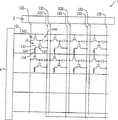
第1図は、本実施の形態における表示装置1の一部を示す回路図であって、この表示装置1は、透明の表示基板上に、複数の走査線131と、これら走査線131に対して交差する方向に延びる複数の信号線132と、これら信号線132に並列に延びる複数の共通給電線133と、がそれぞれ配線された構成を有するとともに、走査線131及び信号線132の各交点毎に、画素領域素1Aが設けられている。
信号線132に対しては、シフトレジスタ、レベルシフタ、ビデオライン、アナログスイッチを備えるデータ側駆動回路3が設けられている。また、走査線131に対しては、シフトレジスタおよびレベルシフタを備える走査側駆動回路4が設けられている。さらに、また、画素領域1Aの各々には、走査線131を介して走査信号がゲート電極に供給されるスイッチング薄膜トランジスタ142と、このスイッチング薄膜トランジスタ142を介して信号線線132から供給される画像信号を保持する保持容量capと、該保持容量capによって保持された画像信号がゲート電極に供給されるカレント薄膜トランジスタ143と、このカレント薄膜トランジスタ143を介して共通給電線133に電気的に接続したときに共通給電線133から駆動電流が流れ込む画素電極141と、この画素電極141と反射電極154との間に挟み込まれる発光素子140と、が設けられている。
かかる構成であれば、走査線131が駆動されてスイッチング薄膜トランジスタ142がオンとなると、その時の信号線132の電位が保持容量capに保持され、該保持容量capの状態に応じて、カレント薄膜トランジスタ143のオン・オフ状態が決まる。そして、カレント薄膜トランジスタ143のチャネルを介して、共通給電線133から画素電極141に電流が流れ、さらに発光素子140を通じて反射電極154に電流が流れるから、発光素子140は、これを流れる電流量に応じて発光する。
ここで、各画素領域1Aの平面構造は、反射電極や発光素子を取り除いた状態での拡大平面図である第2図に示すように、平面形状が長方形の画素電極141の四辺が、信号線132、共通給電線133、走査線131及び図示しない他の画素電極用の走査線によって囲まれた配置となっている。
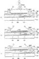
第3図〜第5図は、画素領域1Aの製造過程を順次示す断面図であって、第2図のA−A線断面に相当する。以下、第3図〜第5図に従って、画素領域1Aの製造工程を説明する。
先ず、第3図(a)に示すように、透明の表示基板121に対して、必要に応じて、TEOS(テトラエトキシシラン)や酸素ガスなどを原料ガスとしてプラズマCVD法により厚さが約2000〜5000オングストロームのシリコン酸化膜からなる下地保護膜(図示せず)。を形成する。次いで、表示基板121の温度を約350℃に設定して、下地保護膜の表面にプラズマCVD法により厚さが約300〜700オングストロームのアモルファスのシリコン膜からなる半導体膜200を形成する。次にアモルファスのシリコン膜からなる半導体膜200に対して、レーザアニールまたは固相成長法などの結晶化工程を行い、半導体膜200をポリシリコン膜に結晶化する。レーザアニール法では、例えば、エキシマレーザでビームの長寸が400mmのラインビームを用い、その出力強度はたとえば200mJ/cm2である。ラインビームについてはその短寸方向におけるレーザ強度のピーク値の90%に相当する部分が各領域毎に重なるようにラインビームを走査する。
次いで、第3図(b)に示すように、半導体膜200をパターニングして島状の半導体膜210とし、その表面に対して、TEOS(テトラエトキシシラン)や酸素ガスなどを原料ガスとしてプラズマCVD法により厚さが約600〜1500オングストロームのシリコン酸化膜または窒化膜からなるゲート絶縁膜220を形成する。なお、半導体膜210は、カレント薄膜トランジスタ143のチャネル領域及びソース・ドレイン領域となるものであるが、異なる断面位置においてはスイッチング薄膜トランジスタ142のチャネル領域及びソース・ドレイン領域となる半導体膜も形成されている。つまり、第3図〜第5図に示す製造工程では二種類のトランジスタ142、143が同時に作られるのであるが、同じ手順で作られるため、以下の説明では、トランジスタに関しては、カレント薄膜トランジスタ143についてのみ説明し、スイッチング薄膜トランジスタ142については説明を省略する。
次いで、第3図(c)に示すように、アルミニウム、タンタル、モリブデン、チタン、タングステンなどの金属膜からなる導電膜をスパッタ法により形成した後、パターニングし、ゲート電極143Aを形成する。
この状態で、高濃度のリンイオンを打ち込んで、シリコン薄膜210に、ゲート電極143Aに対して自己整合的にソース・ドレイン領域143a、143bを形成する。なお、不純物が導入されなかった部分がチャネル領域143cとなる。
次いで、第3図(d)に示すように、層間絶縁膜230を形成した後、コンタクトホール232、234を形成し、それらコンタクトホール232、234内に中継電極236、238を埋め込む。
次いで、第3図(e)に示すように、層間絶縁膜230上に、信号線132、共通給電線133及び走査線(第3図には図示せず。)を形成する。このとき、信号線132、共通給電線133及び走査線の各配線は、配線として必要な厚さに捕らわれることなく、十分に厚く形成する。
具体的には、各配線を1〜2μm程度の厚さに形成する。ここで中継電極238と各配線とは、同一工程で形成されていてもよい。この時、中継電極236は、後述するITO膜により形成されることになる。
そして、各配線の上面をも覆うように層間絶縁膜240を形成し、中継電極236に対応する位置にコンタクトホール242を形成し、そのコンタクトホール内にも埋め込まれるようにITO膜を形成し、そのITO膜をパターニングして、信号線132、共通給電線133及び走査線に囲まれた所定位置に、ソース・ドレイン領域143aに電気的に接続する画素電極141を形成する。
ここで、第3図(e)では、信号線132及び共通給電線133に挟まれた部分が、光学材料が選択的に配置される所定位置に相当するものである。そして、その所定位置とその周囲との間には、信号線132や共通給電線133によって段差111が形成されている。具体的には、所定位置の方がその周囲よりも低くなっている凹型の段差111が形成されている。
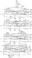
次いで、第4図(a)に示すように、表示基板121の上面を上に向けた状態で、インクジェットヘッド方式により、発光素子140の下層部分に当たる正孔注入層を形成するための液状(溶媒に溶かされた溶液状)の光学材料(前駆体)114Aを吐出し、これを段差111で囲まれた領域内(所定位置)に選択的に塗布する。なお、インクジェット方式の具体的な内容は、本発明の要旨ではないため、省略する(かかる方式については、例えば、特開昭56−13184号公報や特開平2−167751号公報を参照)。
正孔注入層を形成するための材料としては、ポリマー前駆体がポリテトラヒドロチオフェニルフェニレンであるポリフェニレンビニレン、1,1−ビス−(4−N,N−ジトリルアミノフェニル)シクロヘキサン、トリス(8−ヒドロキシキノリノール)アルミニウム等が挙げられる。
このとき、液状の前駆体114Aは、流動性が高いため、水平方向に広がろうとするが、塗布された位置を取り囲むように段差111が形成されているため、その液状の前駆体114Aの1回当たりの塗布量を極端に大量にしなければ、液状の前駆体114Aが段差111を越えて所定位置の外側に広がることは防止される。
次いで、第4図(b)に示すように、加熱或いは光照射により液状の前駆体114Aの溶媒を蒸発させて、画素電極141上に、固形の薄い正孔注入層140aを形成する。ここでは、液状の前駆体114Aの濃度にもよるが、薄い正孔注入層140aしか形成されない。そこで、より厚い正孔注入層140aを必要とする場合には、第4図(a)及び(b)の工程を必要回数繰り返し実行し、第4図(c)に示すように、十分な厚さの正孔注入層140Aを形成する。
次いで、第5図(a)に示すように、表示基板121の上面を上に向けた状態で、インクジェットヘッド方式により、発光素子140の上層部分に当たる有機半導体膜を形成するための液状(溶媒に溶かされた溶液状)の光学材料(有機蛍光材料)114Bを吐出し、これを段差111で囲まれた領域内(所定位置)に選択的に塗布する。
有機蛍光材料としては、シアノポリフェニレンビニレン、ポリフェニレンビニレン、ポリアルキルフェニレン、2,3,6,7−テトラヒドロ−11−オキソ−1H,5H,11H(1)ベンゾピラノ[6,7,8−ij]−キノリジン−10ーカルボン酸、1,1−ビス−(4−N,N−ジトリルアミノフェニル)シクロヘキサン、2−13’,4’−ジヒドロキシフェニル)−3,5,7−トリヒドロキシ−1−ベンゾピリリウムパークロレート、トリス(8−ヒドロキシキノリノール)アルミニウム、2,3,6,7−テトラヒドロ−9−メチル−11−オキソ−1H,5H,11H(1)ベンゾピラノ[6,7,8−ij]−キノリジン、アロマティックジアミン誘導体(TDP)、オキシジアゾールダイマー(OXD)、オキシジアゾール誘導体(PBD)、ジスチルアリーレン誘導体(DSA)、キノリノール系金属錯体、ベリリウム−ベンゾキノリノール錯体(Bebq)、トリフェニルアミン誘導体(MTDATA)、ジスチリル誘導体、ピラゾリンダイマー、ルブレン、キナクリドン、トリアゾール誘導体、ポリフェニレン、ポリアルキルフルオレン、ポリアルキルチオフェン、アゾメチン亜鉛錯体、ポリフィリン亜鉛錯体、ベンゾオキサゾール亜鉛錯体、フェナントロリンユウロピウム錯体等が挙げられる。
このとき、液状の有機蛍光材料114Bは、流動性が高いため、やはり水平方向に広がろうとするが、塗布された位置を取り囲むように段差111が形成されているため、その液状の有機蛍光材料114Bの1回当たりの塗布量を極端に大量にしなければ、液状の有機蛍光材料114Bが段差111を越えて所定位置の外側に広がることは防止される。
次いで、第5図(b)に示すように、加熱或いは光照射により液状の有機蛍光材料114Bの溶媒を蒸発させて、正孔注入層140A上に、固形の薄い有機半導体膜140bを形成する。ここでは、液状の有機蛍光材料114Bの濃度にもよるが、薄い有機半導体膜140bしか形成されない。そこで、より厚い有機半導体膜140bを必要とする場合には、第5図(a)及び(b)の工程を必要回数繰り返し実行し、第5図(c)に示すように、十分な厚さの有機半導体膜140Bを形成する。正孔注入層140A及び有機半導体膜140Bによって、発光素子140が構成される。最後に、第5図(d)に示すように、表示基板121の表面全体に若しくはストライプ状に反射電極154を形成する。
このように、本実施の形態にあっては、発光素子140が配置される処置位置を四方から取り囲むように信号線132、共通配線133等の配線を形成するとともに、それら配線を通常よりも厚く形成して段差111を形成し、そして、液状の前駆体114Aや液状の有機蛍光材料114Bを選択的に塗布するようにしているため、発光素子140のパターニング精度が高いという利点がある。
そして、段差111を形成すると、反射電極154は比較的凹凸の大きな面に形成されることになるが、その反射電極154の厚さをある程度厚くしておけば、断線等の不具合が発生する可能性は極めて小さくなる。
しかも、信号線132や共通配線133等の配線を利用して段差111を形成するため、特に新たな工程が増加する訳ではないから、製造工程の大幅な複雑化等を招くこともない。
なお、液状の前駆体114Aや液状の有機蛍光材料114Bが、段差111の内側から外側に流れ出すことをより確実に防止するためには、液状の前駆体114Aや液状の有機蛍光材料114Bの塗布厚さdaと、段差111の高さdrとの間に、
da<dr ……(1)
という関係が成立するようにしておくことが望ましい。
ただし、液状の有機蛍光材料114Bを塗布する際には、既に正孔注入層140Aが形成されているため、段差111の高さdrは、当初の高さからその正孔注入層140Aの分を差し引いて考えることが必要である。
また、上記(1)式を満足するとともに、さらに、有機半導体膜140Bに印加される駆動電圧Vdと、液状の有機蛍光材料114Bの各塗布厚さの和dbと、液状の有機蛍光材料114Bの濃度rと、有機半導体膜140Bに光学特性変化が現れる最少の電界強度(しきい電界強度)Etとの間に、
Vd/(db・r)>Et ……(2)
という関係が成立するようにすれば、塗布厚さと駆動電圧との関係が明確化され、有機半導体膜140Bの電気光学効果が発現することが補償される。
一方、段差111と発光素子140との平坦性が確保でき、有機半導体膜140Bの光学特性変化の一様性と、短絡の防止を可能とするためには、発光素子140の完成時の暑さdfと、段差111の高さdrとの間に、
df=dr ……(3)
という関係を成立させればよい。
さらに、上記(3)式を満足するとともに、下記の(4)式を満足すれば、発光素子140の完成時の厚さと駆動電圧との関係が明確化され、有機蛍光材料の電気光学効果が発現することが補償される。
Vd/df>Et ……(4)
ただし、この場合のdfは、発光素子140全体ではなく、有機半導体膜140Bの完成時の厚さである。
なお、発光素子140の上層部を形成する光学材料は、有機蛍光材料114Bに限定されるものではなく、無機の蛍光材料であってもよい。
また、スイッチング素子としての各トランジスタ142、143は、600℃以下の低温プロセスで形成された多結晶シリコンにより形成することが望ましく、これにより、ガラス基板の使用による低コスト化と、高移動度による高性能化が両立できる。なお、スイッチング素子は、非晶質シリコンまたは600℃以上の高温プロセスで形成された多結晶シリコンにより形成されてもよい。
そして、スイッチング薄膜トランジスタ142およびカレント薄膜トランジスタ143の他にトランジスタを設ける形式であってもよいし、或いは、一つのトランジスタで駆動する形式であってもよい。
また、段差111は、パッシブマトリクス型表示素子の第1のバス配線、アクティブマトリクス型表示素子の走査線131および、遮光層によって形成してもよい。
なお、発光素子140としては、発光効率(正孔注入率)がやや低下するものの、正孔注入層140Aを省略してもよい。また、正孔注入層140Aに代えて電子注入層を有機半導体膜140Bと反射電極154との間に形成してもよいし、或いは、正孔注入層及び電子注入層の双方を形成してもよい。
また、上記実施の形態では、特にカラー表示を念頭において、各発光素子140全体を選択的に配置した場合について説明したが、例えば単色表示の表示装置1の場合には、第6図に示すように、有機半導体膜140Bは、表示基板121全面に一様に形成してもよい。ただし、この場合でも、クロストークを防止するために正孔注入層140Aは各所定位置毎に選択的に配置しなければならないため、段差111を利用した塗布が極めて有効である。
(2)第2の実施の形態
第7図は本発明の第2の実施の形態を示す図であって、この実施の形態は、本発明に係るマトリクス型表示素子及びその製造方法を、EL表示素子を用いたパッシブマトリクス型の表示装置に適用したものである。
なお、第7図(a)は、複数の第1のバス配線300と、これに直交する方向に配設された複数の第2のバス配線310と、の配置関係を示す平面図であり、第7図(b)は、同(a)のB−B線断面図である。なお、上記第1の実施の形態と同様の構成には、同じ符号を付し、その重複する説明は省略する。また、細かな製造工程等も上記第1の実施の形態と同様であるため、その図示及び説明は省略する。
即ち、本実施の形態にあっては、発光素子140が配置される所定位置を取り囲むように、例えばSiO2等の絶縁膜320が配設されていて、これにより、所定位置とその周囲との間に、段差111が形成されている。
このような構成であっても、上記第1の実施の形態と同様に、液状の前駆体114Aや液状の有機蛍光材料114Bを選択的に塗布する際に、それらが周囲に流れ出ることが防止でき、高精度のパターニングが行える等の利点がある。
(3)第3の実施の形態
第8図は本発明の第3の実施の形態を示す図であって、この実施の形態も、上記第1の実施の形態と同様に、本発明に係るマトリクス型表示素子及びその製造方法を、EL表示素子を用いたアクティブマトリクス型の表示装置に適用したものである。より具体的には、画素電極141を利用して段差111を形成することにより、高精度のパターニングが行えるようにしたものである。なお、上記実施の形態と同様の構成には、同じ符号を付しておく。また、第8図は製造工程の途中を示す断面図であり、その前後は上記第1の実施の形態と略同様であるためその図示及び説明は省略する。
即ち、本実施の形態では、画素電極141を通常よりも厚く形成し、これにより、その周囲と間に段差111を形成している。つまり、本実施の形態では、後に光学材料が塗布される画素電極141の方がその周囲よりも高くなっている凸型の段差が形成されている。
そして、上記第1の実施の形態と同様に、インクジェットヘッド方式により、発光素子140の下層部分に当たる正孔注入層を形成するための液状(溶媒に溶かされた溶液状)の光学材料(前駆体)114Aを吐出し、画素電極141上面に塗布する。
ただし、上記第1の実施の形態の場合とは異なり、表示基板121を上下逆にした状態、つまり液状の前駆体114Aが塗布される画素電極141上面を下方に向けた状態で、液状の前駆体114Aの塗布を行う。
すると、液状の前駆体114Aは、重力と表面張力とによって、画素電極141上面に溜まり、その周囲には広がらない。よって、加熱や光照射等を行って固形化すれば、第4図(b)と同様の薄い正孔注入層を形成でき、これを繰り返せば正孔注入層が形成される。同様の手法で、有機半導体膜も形成される。
このように、本実施の形態では、凸型の段差111を利用して液状の光学材料を塗布して発光素子のパターニング精度を向上することができる。
なお、遠心力等の慣性力を利用して、画素電極141上面に溜まる液状の光学材料の量を調整するようにしてもよい。
(4)第4の実施の形態
第9図は本発明の第4の実施の形態を示す図であって、この実施の形態も、上記第1の実施の形態と同様に、本発明に係るマトリクス型表示素子及びその製造方法を、EL表示素子を用いたアクティブマトリクス型の表示装置に適用したものである。なお、上記実施の形態と同様の構成には、同じ符号を付しておく。また、第9図は製工程の途中を示す断面図であり、その前後は上記第1の実施の形態と略同様であるためその図示及び説明は省略する。
即ち、本実施の形態では、先ず、表示基板121上に、反射電極154を形成し、次いで、反射電極154上に、後に発光素子140が配置される所定位置を取り囲むように絶縁膜320を形成し、これにより所定位置の方がその周囲よりも低くなっている凹型の段差111を形成する。
そして、上記第1の実施の形態と同様に、段差111で囲まれた領域内に、インクジェット方式により液状の光学材料を選択的に塗布することにより、発光素子140を形成する。
一方、剥離用基板122上に、剥離層152を介して、走査線131、信号線132、画素電極141、スイッチング薄膜トランジスタ142、カレント薄膜トランジスタ143および絶縁膜240を形成する。
最後に、表示基板121上に、剥離用基板122上の剥離層122から剥離された構造を転写する。
このように、本実施の形態であっても、段差111を利用して液状の光学材料を塗布するようにしたから、高精度のパターニングが行える。
さらに、本実施の形態では、発光素子140等の下地材料への、その後の工程によるダメージ、あるいは、走査線131、信号線132、画素電極141、スイッチング薄膜トランジスタ142、カレント薄膜トランジスタ143または絶縁膜240への、光学材料の塗布等によるダメージを、軽減することが可能となる。
本実施の形態では、アクティブマトリクス型表示素子として説明したが、パッシブマトリクス型表示素子であってもよい。
(5)第5の実施の形態
第10図は本発明の第6の実施の形態を示す図であって、この実施の形態も、上記第1の実施の形態と同様に、本発明に係るマトリクス型表示素子及びその製造方法を、EL表示素子を用いたアクティブマトリクス型の表示装置に適用したものである。なお、上記実施の形態と同様の構成には、同じ符号を付しておく。また、第10図は製造工程の途中を示す断面図であり、その前後は上記第1の実施の形態と略同様であるためその図示及び説明は省略する。
即ち、本実施の形態では、層間絶縁膜240を利用して凹型の段差111を形成していて、これにより、上記第1の実施の形態と同様の作用効果を得るようにしている。
また、層間絶縁膜240を利用して段差111を形成するため、特に新たな工程が増加する訳ではないから、製造工程の大幅な複雑化等を招くこともない。
(6)第6の実施の形態
第11図は本発明の第6の実施の形態を示す図であって、この実施の形態も、上記第1の実施の形態と同様に、本発明に係るマトリクス型表示素子及びその製造方法を、EL表示素子を用いたアクティブマトリクス型の表示装置に適用したものである。なお、上記実施の形態と同様の構成には、同じ符号を付しておく。また、第11図は製造工程の途中を示す断面図であり、その前後は上記第1の実施の形態と略同様であるためその図示及び説明は省略する。
即ち、本実施の形態では、段差を利用してパターニング精度を向上させるのではなく、液状の光学材料が塗布される所定位置の親水性を、その周囲の親水性よりも相対的に強くすることにより、塗布された液状の光学材料が周囲に広がらないようにしたものである。
具体的には、第11図に示すように、層間絶縁膜240を形成した後に、その上面に非晶質シリコン層155を形成している。非晶質シリコン層155は、画素電極141を形成するITOよりも相対的に撥水性が強いので、ここに、画素電極141表面の親水性がその周囲の親水性よりも相対的に強い撥水性・親水性の分布が形成される。
そして、上記第1の実施の形態と同様に、画素電極141の上面に向けて、インクジェット方式により液状の光学材料を選択的に塗布することにより、発光素子140を形成し、最後に反射電極を形成する。
このように、本実施の形態であっても、所望の撥水性・親液性の分布を形成してから液状の光学材料を塗布するようにしているから、パターニングの精度を向上させることができる。
なお、本実施の形態の場合も、パッシブマトリクス型表示素子に適用できることは勿論である。
また、剥離用基板121上に剥離層152を介して形成された構造を、表示基板121に転写する工程を含んでいてもよい。
さらに、本実施の形態では、所望の撥水性・親水性の分布を、非晶質シリコン層155によって形成しているが、撥水性・親水性の分布は、金属や、陽極酸化膜、ポリイミドまたは酸化シリコン等の絶縁膜や、他の材料により形成されていてもよい。なお、パッシブマトリクス型表示素子であれば第1のバス配線、アクティブマトリクス型表示素子であれば走査線131、信号線132、画素電極141、絶縁膜240或いは遮光層によって形成してもよい。また、本実施の形態では、液状の光学材料が水溶液であることを前提に説明したが、他の液体の溶液を用いた液状の光学材料であってもよく、その場合は、その溶液に対して撥液性・親液性が得られるようにすればよい。
(7)第7の実施の形態
本発明の第7の実施の形態は、断面構造は上記第5の実施の形態で使用した第10図と同様であるため、これを用いて説明する。
即ち、本実施の形態では、層間絶縁膜240をSiO2で形成するとともに、その表面に紫外線を照射し、その後に、画素電極141表面を露出させ、そして液状の光学材料を選択的に塗布するようになっている。
このような製造工程であれば、段差111が形成されるだけでなく、層間絶縁膜240表面に沿って撥液性の強い分布が形成されるため、塗布された液状の光学材料は、段差111と層間絶縁膜240の撥液性との両方の作用によって所定位置に溜まり易くなっている。つまり、上記第5の実施の形態と、上記第6の実施の形態との両方の作用が発揮されるから、さらに発光素子140のパターニング精度を向上させることができる。
なお、紫外線を照射するタイミングは、画素電極141の表面を露出させる前後いずれでもよく、層間絶縁膜240を形成する材料や、画素電極141を形成する材料等に応じて適宜選定すればよく。ちなみに、画素電極141の表面を露出させる前に紫外線を照射する場合には、段差111の内壁面は撥液性が強くならないから、段差111で囲まれた領域に液状の光学材料を溜めることにとって有利である。これとは逆に、画素電極141の表面を露出させた後に紫外線を照射する場合には、段差111の内壁面の撥液性が強くならないように垂直に紫外線を照射する必要があるが、画素電極141の表面を露出する際のエッチング工程の後で紫外線を照射するため、そのエッチング工程によって撥液性が弱まるような懸念がないという利点がある。
また、層間絶縁膜240を形成する材料としては、例えばフォトレジストを用いることもできるし、或いはポリイミドを用いてもよく、これらであればスピンコートにより膜を形成できるという利点がある。
そして、層間絶縁膜240を形成する材料によっては、紫外線を照射するのではなく、例えばO2、CF4、Ar等のプラズマを照射することにより撥液性が強くなるようにしてもよい。
(8)第8の実施の形態
第12図は本発明の第8の実施の形態を示す図であって、この実施の形態も、上記第1の実施の形態と同様に、本発明に係るマトリクス型表示素子及びその製造方法を、EL表示素子を用いたアクティブマトリクス型の表示装置に適用したものである。なお、上記実施の形態と同様の構成には、同じ符号を付しておく。また、第12図は製造工程の途中を示す断面図であり、その前後は上記第1の実施の形態と略同様であるためその図示及び説明は省略する。
即ち、本実施の形態では、段差や撥液性・親液性の分布等を利用してパターニング精度を向上させるのではなく、電位による引力や斥力を利用してパターニング精度の向上を図っている。
つまり、第12図に示すように、信号線132や共通給電線133を駆動するとともに、図示しないトランジスタを適宜オン・オフすることにより、画素電極141がマイナス電位となり、層間絶縁膜240がプラス電位となる電位分布を形成する。そして、インクジェット方式により、プラスに帯電した液状の光学材料114を所定位置に選択的に塗布する。
このように、本実施の形態であれば、表示基板121上に所望の電位分布を形成し、その電位分布と、プラスに帯電した液状の光学材料114との間の引力及び斥力を利用して、液状の光学材料を選択的に塗布しているから、パターニングの精度を向上させることができる。
特に、本実施の形態では、液状の光学材料114を帯電させているので、自発分極だけでなく帯電電荷も利用することにより、パターニングの精度を向上する効果が、さらに高まる。
本実施の形態では、アクティブマトリクス型表示素子に適用した場合を示しているが、パッシブマトリクス型表示素子であっても適用可能である。
なお、剥離用基板121上に剥離層152を介して形成された構造を、表示基板121に転写する工程を含んでいてもよい。
また、本実施の形態では、所望の電位分布は、走査線131に順次電位を印加し、同時に信号線132および共通線133に電位を印加し、画素電極141にスイッチング薄膜トランジスタ142およびカレント薄膜トランジスタ143を介して電位を印加することにより形成される。
電位分布を走査線131、信号線132、共通線133および画素電極141で形成することにより、工程の増加が抑制できる。なお、パッシブマトリクス型表示素子であれば、電位分布は、第1のバス配線および遮光層によって形成することができる。
さらに、本実施の形態では、画素電極141と、その周囲の層間絶縁膜240との両方に電位を与えているが、これに限定されるものではなく、例えば第13図に示すように、画素電極141には電位を与えず、層間絶縁膜240にのみプラス電位を与え、そして、液状の光学材料114をプラスに帯電させてから塗布するようにしてもよい。このようにすれば、塗布された後にも、液状の光学材料114は確実にプラスに帯電した状態を維持できるから、周囲の層間絶縁膜240との間の斥力によって、液状の光学材料114が周囲に流れ出ることをより確実に防止することができるようになる。
なお、上記各実施の形態で説明したものとは異なり、例えば、段差111を、液状の材料を塗布することにより形成してもよいし、或いは、段差111を、剥離用基板上に剥離層を介して材料を形成し、表示基板上に剥離用基板上に剥離層から剥離された構造を転写することにより形成してもよい。
また、上記各実施の形態では、光学材料として有機又は無機のELが適用可能であるとして説明したが、これに限定されるものではなく、光学材料は液晶であってもよい。
産業上の利用可能性
以上説明したように、本発明によれば、発光材料を所定の第1バス配線と第2バス配線の内側の第一電極に対向する位置に的確に塗布することができ、液状の発光材料が周囲に広がることを防ぐことができる。
【図面の簡単な説明】
【図1】本発明の第1の実施の形態における表示装置の一部を示す回路図である。
【図2】画素領域の平面構造を示す拡大平面図である。
【図3】第1の実施の形態における製造工程の流れを示す断面図である。
【図4】第1の実施の形態における製造工程の流れを示す断面図である。
【図5】第1の実施の形態における製造工程の流れを示す断面図である。
【図6】第1の実施の形態の変形例を示す断面図である。
【図7】第2の実施の形態を示す平面図及び断面図である。
【図8】第3の実施の形態の製造工程の一部を示す断面図である。
【図9】第4の実施の形態の製造工程の一部を示す断面図である。
【図10】第5の実施の形態の製造工程の一部を示す断面図である。
【図11】第6の実施の形態の製造工程の一部を示す断面図である。
【図12】第8の実施の形態の製造工程の一部を示す断面図である。
【図13】第8の実施の形態の変形例を示す断面図である。BACKGROUND OF THE INVENTION
The present invention relates to a display element in which an optical agent such as a fluorescent material (light emitting material) or a light modulation material is selectively disposed at a predetermined position on a display substrate.
[Background]
Matrix-type display elements such as LCD (Liquid Crystal Display) and EL (Electroluminescense) display elements are used in various types and in large numbers as display elements that realize light weight, thinness, high image quality, and high definition. The matrix type display element includes a matrix-like bus wiring, an optical material (light emitting material or light modulation material), and another structure as necessary.
Here, in the case of a single-color matrix display element, wirings and electrodes need to be arranged in a matrix on the display substrate, but the optical material can be uniformly applied to the entire surface of the display substrate.
On the other hand, for example, when a so-called color matrix type display element is to be realized by an EL display element that emits light by itself, three pixel electrodes are arranged for each pixel corresponding to the three primary colors of RGB light. In addition, an optical material corresponding to one of RGB must be applied to each pixel electrode. That is, it is necessary to selectively arrange the optical material at a predetermined position.
Therefore, development of a method for patterning an optical material is desired, but examples of effective patterning methods include etching and coating.
The process in the case of etching is as follows.
First, a layer of an optical material is formed on a display substrate. Next, a resist film is formed on the optical material layer, and the resist film is exposed through a mask and then patterned. Etching is then performed to pattern the optical material layer in accordance with the resist pattern.
However, in this case, since the number of processes is large and each material and apparatus are expensive, the cost becomes high. Further, since the number of processes is large and each process is complicated, the throughput is also poor. Furthermore, depending on the chemical properties of the optical material, the resistance to resists and etchants is low, and these processes may not be possible.
On the other hand, the process in the case of application is as follows.
First, an optical material is dissolved in a solvent to form a liquid, and this liquid optical material is selectively applied to a predetermined position on the display substrate by an inkjet method or the like. Then, if necessary, the optical material is solidified by heating, light irradiation, or the like. In this case, the number of processes is small, and the cost is reduced because each material and device are inexpensive. Further, since the number of processes is small and each process is simple, the throughput is good. Furthermore, these steps are possible if liquefaction can be achieved regardless of the chemical properties of the optical material.
[Problems to be solved by the invention]
The patterning method by coating as described above seems to be easily implemented at first glance. However, when applying an optical material by an ink jet method, the optical material must be diluted several tens of times with a solvent, so its fluidity is high, and after application, the application position is completely solidified. It has proved difficult to hold on.
That is, the patterning accuracy is poor due to the fluidity of the liquid optical material. For example, when the optical material applied to a certain pixel flows out to an adjacent pixel, the optical characteristics of the pixel are deteriorated. In addition, since the application area varies for each pixel, the application thickness varies, and the optical characteristics of the optical material also vary.
Such a problem is noticeable in a light emitting material for an EL display element which is liquid when applied and is solidified later, but liquid crystal which is liquid when applied and thereafter is selectively formed on a display substrate. This is also a problem that occurs in the same manner when applied to the coating.
The present invention has been made paying attention to such an unsolved problem of the conventional technique, and maintains the characteristics such as low cost, high throughput, and high degree of freedom of optical materials while maintaining the liquid state. It is an object of the present invention to provide a method of manufacturing a display element that can reliably arrange the optical material at a predetermined position.
[Means for Solving the Problems]
The method for manufacturing a light emitting device of the present invention controls a first electrode, a second electrode, a light emitting material layer disposed between the first electrode and the second electrode, and the first electrode on a substrate. A method of manufacturing a light emitting device having a scanning line, a signal line, and a common power supply line connected to any of a plurality of switching elements arranged for
The scanning line, the signal line intersecting the scanning line, and a common power supply line provided in parallel with the signal line are arranged on the substrate, and a step is formed by the scanning line, the signal line, and the common power supply line. ,
Forming the first electrode at a predetermined position of a recess surrounded by steps of the scanning line, the signal line and the common power supply line;
A light emitting material is selectively applied by an ink jet method to a position facing the first electrode in the step, and a light emitting material layer is formed in a region inside the recess,
Thereafter, the second electrode is formed to face the first electrode.
Features.
The method for manufacturing a light emitting device according to the present invention is characterized in that the scanning line, the signal line, and the common feeder line have a film thickness larger than that of the light emitting material layer.
The method for manufacturing a light emitting device according to the present invention includes a step of forming an insulating film on the scanning line, the signal line, and the common power supply line.
DETAILED DESCRIPTION OF THE INVENTION
Hereinafter, preferred embodiments of the present invention will be described with reference to the drawings.
(1) First embodiment
FIG. 1 to FIG. 5 are diagrams showing a first embodiment of the present invention. In this embodiment, the matrix display element and the manufacturing method thereof according to the present invention are applied to an EL display element. The present invention is applied to an active matrix type display device. More specifically, an example is shown in which a light emitting material as an optical material is applied using a scanning line, a signal line, and a common power supply line as wiring.
FIG. 1 is a circuit diagram showing a part of the display device 1 according to the present embodiment. The display device 1 has a plurality of
For the
With this configuration, when the
Here, the planar structure of each
3 to 5 are cross-sectional views sequentially showing the manufacturing process of the
First, as shown in FIG. 3 (a), a
Next, as shown in FIG. 3B, the
Next, as shown in FIG. 3C, a conductive film made of a metal film such as aluminum, tantalum, molybdenum, titanium, or tungsten is formed by sputtering, followed by patterning to form a
In this state, high concentration phosphorus ions are implanted to form source /
Next, as shown in FIG. 3D, after the
Next, as shown in FIG. 3 (e), a
Specifically, each wiring is formed to a thickness of about 1 to 2 μm. Here, the
Then, an
Here, in FIG. 3 (e), a portion sandwiched between the
Next, as shown in FIG. 4 (a), a liquid (solvent) for forming a hole injection layer corresponding to the lower layer portion of the
As a material for forming the hole injection layer, polyphenylene vinylene whose polymer precursor is polytetrahydrothiophenylphenylene, 1,1-bis- (4-N, N-ditolylaminophenyl) cyclohexane, tris (8 -Hydroxyquinolinol) aluminum and the like.
At this time, the
Next, as shown in FIG. 4B, the solvent of the
Next, as shown in FIG. 5 (a), the liquid (for the solvent) for forming the organic semiconductor film corresponding to the upper layer portion of the
As organic fluorescent materials, cyanopolyphenylene vinylene, polyphenylene vinylene, polyalkylphenylene, 2,3,6,7-tetrahydro-11-oxo-1H, 5H, 11H (1) benzopyrano [6,7,8-ij]- Quinolidine-10-carboxylic acid, 1,1-bis- (4-N, N-ditolylaminophenyl) cyclohexane, 2-13 ′, 4′-dihydroxyphenyl) -3,5,7-trihydroxy-1-benzo Pyrylium perchlorate, tris (8-hydroxyquinolinol) aluminum, 2,3,6,7-tetrahydro-9-methyl-11-oxo-1H, 5H, 11H (1) benzopyrano [6,7,8-ij] -Quinolidine, aromatic diamine derivative (TDP), oxydiazole dimer (OXD), oxydia Derivative (PBD), distilarylene derivative (DSA), quinolinol-based metal complex, beryllium-benzoquinolinol complex (Bebq), triphenylamine derivative (MTDATA), distyryl derivative, pyrazoline dimer, rubrene, quinacridone, triazole derivative , Polyphenylene, polyalkylfluorene, polyalkylthiophene, azomethine zinc complex, porphyrin zinc complex, benzoxazole zinc complex, phenanthroline europium complex, and the like.
At this time, since the liquid
Next, as shown in FIG. 5B, the solvent of the liquid
As described above, in the present embodiment, the
When the
In addition, since the
In order to more reliably prevent the
da <dr (1)
It is desirable to establish such a relationship.
However, when the liquid
In addition to satisfying the above equation (1), the driving voltage Vd applied to the
Vd / (db · r)> Et (2)
If this relationship is established, the relationship between the coating thickness and the drive voltage is clarified, and it is compensated that the electro-optical effect of the
On the other hand, in order to ensure the flatness between the
df = dr (3)
This relationship should be established.
Furthermore, if the above equation (3) is satisfied and the following equation (4) is satisfied, the relationship between the thickness of the
Vd / df> Et (4)
However, df in this case is the thickness when the
The optical material forming the upper layer portion of the
The
In addition to the switching
The
Note that the light-emitting
Further, in the above-described embodiment, the case where the entire
(2) Second embodiment
FIG. 7 is a diagram showing a second embodiment of the present invention. In this embodiment, a matrix type display element and a manufacturing method thereof according to the present invention are applied to a passive matrix type using an EL display element. This is applied to a display device.
FIG. 7A is a plan view showing an arrangement relationship between the plurality of
That is, in the present embodiment, for example, SiO 2 is surrounded so as to surround a predetermined position where the
Even with such a configuration, when the
(3) Third embodiment
FIG. 8 is a diagram showing a third embodiment of the present invention. This embodiment also shows a matrix type display element and a method for manufacturing the same according to the present invention, as in the first embodiment. The present invention is applied to an active matrix display device using an EL display element. More specifically, the
That is, in the present embodiment, the
As in the first embodiment, a liquid (solution dissolved in a solvent) optical material (precursor) for forming a hole injection layer corresponding to the lower layer portion of the
However, unlike the case of the first embodiment, the liquid precursor is displayed with the
Then, the
As described above, in this embodiment mode, it is possible to improve the patterning accuracy of the light emitting element by applying the liquid optical material using the
Note that the amount of liquid optical material accumulated on the upper surface of the
(4) Fourth embodiment
FIG. 9 is a diagram showing a fourth embodiment of the present invention. This embodiment also shows a matrix type display device and a method for manufacturing the same according to the present invention, as in the first embodiment. The present invention is applied to an active matrix display device using an EL display element. In addition, the same code | symbol is attached | subjected to the structure similar to the said embodiment. FIG. 9 is a cross-sectional view showing the middle of the manufacturing process, and the front and rear thereof are substantially the same as those in the first embodiment, and the illustration and description thereof are omitted.
That is, in this embodiment mode, first, the
Then, similarly to the first embodiment, a light-emitting
On the other hand, the
Finally, the structure peeled off from the
Thus, even in this embodiment, since the liquid optical material is applied using the
Further, in this embodiment mode, damage to a base material such as the light-emitting
In this embodiment mode, the active matrix display element is described. However, a passive matrix display element may be used.
(5) Fifth embodiment
FIG. 10 is a diagram showing a sixth embodiment of the present invention, and this embodiment also shows a matrix type display element and a method for manufacturing the same according to the present invention, as in the first embodiment. The present invention is applied to an active matrix display device using an EL display element. In addition, the same code | symbol is attached | subjected to the structure similar to the said embodiment. Further, FIG. 10 is a cross-sectional view showing the middle of the manufacturing process, and before and after that, since it is substantially the same as the first embodiment, its illustration and description are omitted.
That is, in the present embodiment, the
Further, since the
(6) Sixth embodiment
FIG. 11 is a diagram showing a sixth embodiment of the present invention, and this embodiment also shows a matrix type display device and a method for manufacturing the same according to the present invention, as in the first embodiment. The present invention is applied to an active matrix display device using an EL display element. In addition, the same code | symbol is attached | subjected to the structure similar to the said embodiment. Further, FIG. 11 is a cross-sectional view showing the middle of the manufacturing process, and the front and rear thereof are substantially the same as those in the first embodiment, and the illustration and description thereof are omitted.
In other words, in this embodiment, the patterning accuracy is not improved by using a step, but the hydrophilicity at a predetermined position where the liquid optical material is applied is made relatively stronger than the surrounding hydrophilicity. Thus, the applied liquid optical material is prevented from spreading around.
Specifically, as shown in FIG. 11, after the
As in the first embodiment, a light-emitting
As described above, even in the present embodiment, since the liquid optical material is applied after the desired water repellency / lyophilic distribution is formed, the patterning accuracy can be improved. .
Needless to say, this embodiment can also be applied to a passive matrix display element.
Further, a step of transferring the structure formed over the peeling
Further, in the present embodiment, the desired water repellency / hydrophilic distribution is formed by the
(7) Seventh embodiment
In the seventh embodiment of the present invention, the cross-sectional structure is the same as that of FIG. 10 used in the fifth embodiment, so that this will be described.
That is, in this embodiment, the
In such a manufacturing process, not only the
Note that the timing of irradiating the ultraviolet rays may be either before or after exposing the surface of the
In addition, as a material for forming the
Depending on the material for forming the
(8) Eighth embodiment
FIG. 12 is a diagram showing an eighth embodiment of the present invention, and this embodiment also shows a matrix type display element and a method for manufacturing the same according to the present invention, as in the first embodiment. The present invention is applied to an active matrix display device using an EL display element. In addition, the same code | symbol is attached | subjected to the structure similar to the said embodiment. Further, FIG. 12 is a cross-sectional view showing the middle of the manufacturing process, and the front and rear thereof are substantially the same as those in the first embodiment, and the illustration and description thereof are omitted.
That is, in this embodiment, the patterning accuracy is improved by using the attractive force or repulsive force due to the potential, instead of using the step, the liquid repellency / lyophilic distribution, or the like. .
That is, as shown in FIG. 12, the
As described above, in the present embodiment, a desired potential distribution is formed on the
In particular, in the present embodiment, since the liquid
Although this embodiment mode shows a case where the present invention is applied to an active matrix display element, the present invention can also be applied to a passive matrix display element.
Note that a step of transferring the structure formed over the
In this embodiment mode, the desired potential distribution is such that the potential is sequentially applied to the
By forming the potential distribution with the
Furthermore, in this embodiment, a potential is applied to both the
Note that unlike those described in the above embodiments, for example, the
In each of the above embodiments, an organic or inorganic EL is applicable as an optical material. However, the present invention is not limited to this, and the optical material may be a liquid crystal.
Industrial applicability
As described above, according to the present invention, the light emitting material can be accurately applied to the position facing the first electrode inside the predetermined first bus wiring and the second bus wiring. It can be prevented from spreading around.
[Brief description of the drawings]
FIG. 1 is a circuit diagram showing a part of a display device according to a first embodiment of the present invention.
FIG. 2 is an enlarged plan view showing a planar structure of a pixel region.
FIG. 3 is a cross-sectional view showing a flow of a manufacturing process in the first embodiment.
FIG. 4 is a cross-sectional view showing the flow of manufacturing steps in the first embodiment.
FIG. 5 is a cross-sectional view showing the flow of the manufacturing process in the first embodiment.
FIG. 6 is a cross-sectional view showing a modification of the first embodiment.
7A and 7B are a plan view and a cross-sectional view illustrating a second embodiment.
FIG. 8 is a cross-sectional view showing a part of the manufacturing process of the third embodiment.
FIG. 9 is a cross-sectional view showing a part of the manufacturing process of the fourth embodiment.
FIG. 10 is a cross-sectional view showing a part of the manufacturing process of the fifth embodiment.
FIG. 11 is a cross-sectional view showing a part of the manufacturing process of the sixth embodiment.
FIG. 12 is a cross-sectional view showing a part of the manufacturing process of the eighth embodiment.
FIG. 13 is a cross-sectional view showing a modification of the eighth embodiment.
Claims (3)
Translated fromJapanese前記基板上に前記走査線、前記走査線と交差する前記信号線及び前記信号線と平行に設けられた共通給電線を配置して、該走査線、信号線及び共通給電線により段差を形成し、
前記走査線、信号線及び共通給電線の段差により囲まれた凹部の所定位置に前記第1電極を形成し、
前記段差内の前記第1電極に対向する位置にインクジェット法により発光材料を選択的に塗布して、前記凹部の内側の領域に発光材料層を形成し、
しかる後に前記第1電極に対向するように前記第2電極を形成することを
特徴とする発光装置の製造方法。A first electrode, a second electrode, a light emitting material layer disposed between the first electrode and the second electrode, and a plurality of switching elements disposed to control the first electrode on a substrate. A method of manufacturing a light emitting device having a scanning line, a signal line, and a common power supply line connected to any of
The scanning line, the signal line intersecting the scanning line, and a common power supply line provided in parallel with the signal line are arranged on the substrate, and a step is formed by the scanning line, the signal line, and the common power supply line. ,
Forming the first electrode at a predetermined position of a recess surrounded by steps of the scanning line, the signal line and the common power supply line;
A light emitting material is selectively applied by an ink jet method to a position facing the first electrode in the step, and a light emitting material layer is formed in a region inside the recess,
Thereafter, the second electrode is formed so as to face the first electrode.
Applications Claiming Priority (2)
| Application Number | Priority Date | Filing Date | Title |
|---|---|---|---|
| JP24808796 | 1996-09-19 | ||
| PCT/JP1997/003297WO1998012689A1 (en) | 1996-09-19 | 1997-09-18 | Matrix type display device and method of production thereof |
Related Child Applications (6)
| Application Number | Title | Priority Date | Filing Date |
|---|---|---|---|
| JP2002330875ADivisionJP3770225B2 (en) | 1996-09-19 | 2002-11-14 | Manufacturing method of substrate for organic EL element |
| JP2002330873ADivisionJP3858810B2 (en) | 1996-09-19 | 2002-11-14 | Method for manufacturing light emitting device |
| JP2002330872ADivisionJP3858809B2 (en) | 1996-09-19 | 2002-11-14 | Method for manufacturing light emitting device |
| JP2002330874ADivisionJP3900068B2 (en) | 1996-09-19 | 2002-11-14 | Method for manufacturing light emitting device |
| JP2004017285ADivisionJP2004253375A (en) | 1996-09-19 | 2004-01-26 | Method for forming organic semiconductor film and method for manufacturing light emitting element |
| JP2004217364ADivisionJP3858916B2 (en) | 1996-09-19 | 2004-07-26 | Method for manufacturing light emitting device |
Publications (1)
| Publication Number | Publication Date |
|---|---|
| JP3786427B2true JP3786427B2 (en) | 2006-06-14 |
Family
ID=17173021
Family Applications (2)
| Application Number | Title | Priority Date | Filing Date |
|---|---|---|---|
| JP50681398AExpired - LifetimeJP3786427B2 (en) | 1996-09-19 | 1997-09-18 | Method for manufacturing light emitting device |
| JP2008054485APendingJP2008210808A (en) | 1996-09-19 | 2008-03-05 | Manufacturing method of display element |
Family Applications After (1)
| Application Number | Title | Priority Date | Filing Date |
|---|---|---|---|
| JP2008054485APendingJP2008210808A (en) | 1996-09-19 | 2008-03-05 | Manufacturing method of display element |
Country Status (8)
| Country | Link |
|---|---|
| US (3) | US20060210704A1 (en) |
| EP (4) | EP0862156B1 (en) |
| JP (2) | JP3786427B2 (en) |
| KR (4) | KR100572238B1 (en) |
| CN (5) | CN100485904C (en) |
| DE (3) | DE69733057T2 (en) |
| TW (1) | TW438992B (en) |
| WO (1) | WO1998012689A1 (en) |
Families Citing this family (127)
| Publication number | Priority date | Publication date | Assignee | Title |
|---|---|---|---|---|
| CN100485904C (en) | 1996-09-19 | 2009-05-06 | 精工爱普生株式会社 | Matrix type display device and manufacturing method thereof |
| JP3520396B2 (en) | 1997-07-02 | 2004-04-19 | セイコーエプソン株式会社 | Active matrix substrate and display device |
| CN100517424C (en)* | 1997-08-21 | 2009-07-22 | 精工爱普生株式会社 | display device |
| JP3729196B2 (en)* | 1997-08-21 | 2005-12-21 | セイコーエプソン株式会社 | Organic electroluminescence device |
| JP3803342B2 (en)* | 1997-08-21 | 2006-08-02 | セイコーエプソン株式会社 | Method for forming organic semiconductor film and method for manufacturing active matrix substrate |
| JP3690406B2 (en)* | 1997-08-21 | 2005-08-31 | セイコーエプソン株式会社 | Organic electroluminescence device |
| JP3803355B2 (en)* | 1997-08-21 | 2006-08-02 | セイコーエプソン株式会社 | Method for manufacturing organic electroluminescence device |
| JP3729195B2 (en)* | 1997-08-21 | 2005-12-21 | セイコーエプソン株式会社 | Organic electroluminescence device and manufacturing method thereof |
| CN100530759C (en)* | 1998-03-17 | 2009-08-19 | 精工爱普生株式会社 | Thin film pattering substrate and surface treatment |
| US20030148024A1 (en)* | 2001-10-05 | 2003-08-07 | Kodas Toivo T. | Low viscosity precursor compositons and methods for the depositon of conductive electronic features |
| JP4258860B2 (en)* | 1998-09-04 | 2009-04-30 | セイコーエプソン株式会社 | Device with light transmission means |
| US6221438B1 (en)* | 1998-11-03 | 2001-04-24 | Sarnoff Corporation | Patterned deposition of a material |
| JP3900724B2 (en)* | 1999-01-11 | 2007-04-04 | セイコーエプソン株式会社 | Organic EL element manufacturing method and organic EL display device |
| US6576926B1 (en)* | 1999-02-23 | 2003-06-10 | Semiconductor Energy Laboratory Co., Ltd. | Semiconductor device and fabrication method thereof |
| JP4524810B2 (en)* | 1999-04-12 | 2010-08-18 | カシオ計算機株式会社 | Organic EL device |
| JP2000323276A (en)* | 1999-05-14 | 2000-11-24 | Seiko Epson Corp | Method for manufacturing organic EL device, organic EL device, and ink composition |
| JP4515349B2 (en)* | 1999-06-04 | 2010-07-28 | 株式会社半導体エネルギー研究所 | Electro-optic device |
| JP4515469B2 (en)* | 1999-06-04 | 2010-07-28 | 株式会社半導体エネルギー研究所 | Method for manufacturing electro-optical device |
| JP4094437B2 (en)* | 1999-06-04 | 2008-06-04 | 株式会社半導体エネルギー研究所 | Method for manufacturing electro-optical device |
| US7288420B1 (en) | 1999-06-04 | 2007-10-30 | Semiconductor Energy Laboratory Co., Ltd. | Method for manufacturing an electro-optical device |
| JP2001052864A (en)* | 1999-06-04 | 2001-02-23 | Semiconductor Energy Lab Co Ltd | Making method of opto-electronical device |
| TW512543B (en) | 1999-06-28 | 2002-12-01 | Semiconductor Energy Lab | Method of manufacturing an electro-optical device |
| JP2001085162A (en)* | 1999-09-10 | 2001-03-30 | Sharp Corp | Organic light emitting device and method of manufacturing the same |
| JP2001110575A (en) | 1999-10-04 | 2001-04-20 | Sanyo Electric Co Ltd | Electroluminescence display device |
| JP4780826B2 (en)* | 1999-10-12 | 2011-09-28 | 株式会社半導体エネルギー研究所 | Method for manufacturing electro-optical device |
| TW468283B (en) | 1999-10-12 | 2001-12-11 | Semiconductor Energy Lab | EL display device and a method of manufacturing the same |
| TW480722B (en) | 1999-10-12 | 2002-03-21 | Semiconductor Energy Lab | Manufacturing method of electro-optical device |
| TW471011B (en) | 1999-10-13 | 2002-01-01 | Semiconductor Energy Lab | Thin film forming apparatus |
| JP2001126867A (en)* | 1999-10-26 | 2001-05-11 | Seiko Epson Corp | Display device manufacturing method |
| US6580094B1 (en)* | 1999-10-29 | 2003-06-17 | Semiconductor Energy Laboratory Co., Ltd. | Electro luminescence display device |
| CN1187846C (en)* | 1999-11-29 | 2005-02-02 | 皇家菲利浦电子有限公司 | Organic electrotuminescent device and method of manufacturing thereof |
| TW465122B (en) | 1999-12-15 | 2001-11-21 | Semiconductor Energy Lab | Light-emitting device |
| JP4533489B2 (en)* | 2000-01-28 | 2010-09-01 | 大日本印刷株式会社 | Image display medium and manufacturing method thereof |
| US6559594B2 (en)* | 2000-02-03 | 2003-05-06 | Semiconductor Energy Laboratory Co., Ltd. | Light-emitting device |
| TW495808B (en) | 2000-02-04 | 2002-07-21 | Semiconductor Energy Lab | Thin film formation apparatus and method of manufacturing self-light-emitting device using thin film formation apparatus |
| JP2001230077A (en)* | 2000-02-18 | 2001-08-24 | Dainippon Printing Co Ltd | Method for manufacturing electroluminescent element |
| TW525305B (en) | 2000-02-22 | 2003-03-21 | Semiconductor Energy Lab | Self-light-emitting device and method of manufacturing the same |
| JP4831873B2 (en)* | 2000-02-22 | 2011-12-07 | 株式会社半導体エネルギー研究所 | Self-luminous device and manufacturing method thereof |
| KR20010085420A (en)* | 2000-02-23 | 2001-09-07 | 기타지마 요시토시 | Electroluminescence element and method manufacturing the same |
| JP4601842B2 (en)* | 2000-02-28 | 2010-12-22 | 株式会社半導体エネルギー研究所 | Thin film formation method |
| JP4637391B2 (en)* | 2000-03-27 | 2011-02-23 | 株式会社半導体エネルギー研究所 | Method for manufacturing light emitting device |
| JP4618918B2 (en)* | 2000-03-27 | 2011-01-26 | 株式会社半導体エネルギー研究所 | Method for manufacturing self-luminous device |
| JP4637390B2 (en)* | 2000-03-27 | 2011-02-23 | 株式会社半導体エネルギー研究所 | Method for manufacturing light emitting device |
| TW521226B (en)* | 2000-03-27 | 2003-02-21 | Semiconductor Energy Lab | Electro-optical device |
| US6852994B2 (en) | 2000-03-31 | 2005-02-08 | Seiko Epson Corporation | Organic EL device and method of manufacturing organic EL device |
| JP4048687B2 (en)* | 2000-04-07 | 2008-02-20 | セイコーエプソン株式会社 | ORGANIC EL ELEMENT AND METHOD FOR PRODUCING ORGANIC EL ELEMENT |
| KR100649722B1 (en) | 2000-04-21 | 2006-11-24 | 엘지.필립스 엘시디 주식회사 | Patterning device for electroluminescent display device and patterning method using same |
| US6356031B1 (en)* | 2000-05-03 | 2002-03-12 | Time Warner Entertainment Co, Lp | Electroluminescent plastic devices with an integral thin film solar cell |
| JP4713010B2 (en)* | 2000-05-08 | 2011-06-29 | 株式会社半導体エネルギー研究所 | Light emitting device and manufacturing method thereof |
| JP4860052B2 (en)* | 2000-05-12 | 2012-01-25 | 株式会社半導体エネルギー研究所 | Light emitting device |
| JP2002083689A (en)* | 2000-06-29 | 2002-03-22 | Semiconductor Energy Lab Co Ltd | Luminescence device |
| JP2002015866A (en)* | 2000-06-30 | 2002-01-18 | Seiko Epson Corp | Manufacturing method of organic EL display |
| JP3943900B2 (en)* | 2000-11-09 | 2007-07-11 | 株式会社東芝 | Self-luminous display device |
| US6980272B1 (en) | 2000-11-21 | 2005-12-27 | Sarnoff Corporation | Electrode structure which supports self alignment of liquid deposition of materials |
| JP3628997B2 (en)* | 2000-11-27 | 2005-03-16 | セイコーエプソン株式会社 | Method for manufacturing organic electroluminescence device |
| CN1921136B (en)* | 2000-11-27 | 2012-05-09 | 精工爱普生株式会社 | Organic electroluminescent device, and manufacture method thereof |
| SG143946A1 (en) | 2001-02-19 | 2008-07-29 | Semiconductor Energy Lab | Light emitting device and method of manufacturing the same |
| JP2002373781A (en)* | 2001-03-29 | 2002-12-26 | Hitachi Ltd | Organic EL display and color filter manufacturing equipment |
| JP3599047B2 (en) | 2001-06-25 | 2004-12-08 | セイコーエプソン株式会社 | Color filter and method of manufacturing the same, droplet material landing accuracy test substrate for color filter, method of measuring droplet material landing accuracy, electro-optical device, and electronic apparatus |
| JP4766218B2 (en)* | 2001-07-09 | 2011-09-07 | セイコーエプソン株式会社 | Organic EL array exposure head, manufacturing method thereof, and image forming apparatus using the same |
| US6845016B2 (en)* | 2001-09-13 | 2005-01-18 | Seiko Epson Corporation | Electronic device and method of manufacturing the same, and electronic instrument |
| JP3705264B2 (en) | 2001-12-18 | 2005-10-12 | セイコーエプソン株式会社 | Display device and electronic device |
| US7109653B2 (en) | 2002-01-15 | 2006-09-19 | Seiko Epson Corporation | Sealing structure with barrier membrane for electronic element, display device, electronic apparatus, and fabrication method for electronic element |
| CN101673508B (en) | 2002-01-18 | 2013-01-09 | 株式会社半导体能源研究所 | Light-emitting device |
| EP1474835A1 (en)* | 2002-02-01 | 2004-11-10 | Koninklijke Philips Electronics N.V. | Structured polmer substrate for ink-jet printing of an oled matrix |
| KR20040081783A (en)* | 2002-02-12 | 2004-09-22 | 이데미쓰 고산 가부시키가이샤 | Organic el display and its production method |
| JP3951750B2 (en)* | 2002-03-07 | 2007-08-01 | セイコーエプソン株式会社 | Substance filling method, film forming method, device and device manufacturing method |
| GB0216055D0 (en)* | 2002-03-20 | 2002-08-21 | Koninkl Philips Electronics Nv | Active matrix electroluminescent display devices and their manufacture |
| US7208760B2 (en)* | 2002-03-20 | 2007-04-24 | Koninklijke Philips Electronics N.V. | Active matrix electroluminescent display devices, and their manufacture |
| GB0216053D0 (en)* | 2002-03-20 | 2002-08-21 | Koninkl Philips Electronics Nv | Active matrix electroluminescent display devices and their manufacture |
| GB0216057D0 (en)* | 2002-03-20 | 2002-08-21 | Koninkl Philips Electronics Nv | Active matrix display devices and their manufacture |
| US7358529B2 (en)* | 2002-03-20 | 2008-04-15 | Koninklijke Philips Electronics N.V. | Active matrix display devices, and their manufacture |
| GB0216058D0 (en)* | 2002-03-20 | 2002-08-21 | Koninkl Philips Electronics Nv | Active matrix electroluminscent display devices and their manufacture |
| JP4053040B2 (en) | 2002-04-26 | 2008-02-27 | 三洋電機株式会社 | Display device |
| US7242441B2 (en)* | 2002-06-10 | 2007-07-10 | Seiko Epson Corporation | Method for manufacturing electro-optical device, and electro-optical device and electronic device manufactured with this manufacturing method |
| US6858464B2 (en) | 2002-06-19 | 2005-02-22 | Semiconductor Energy Laboratory Co., Ltd. | Method of manufacturing light emitting device |
| JP2004055159A (en)* | 2002-07-16 | 2004-02-19 | Dainippon Screen Mfg Co Ltd | Method for manufacturing organic el element, and organic el element displaying device |
| WO2004026002A1 (en)* | 2002-09-11 | 2004-03-25 | Semiconductor Energy Laboratory Co., Ltd. | Light-emitting apparatus and fabrication method of the same |
| JP2004127933A (en)* | 2002-09-11 | 2004-04-22 | Semiconductor Energy Lab Co Ltd | Light-emitting apparatus and fabrication method of the same |
| JP3719431B2 (en) | 2002-09-25 | 2005-11-24 | セイコーエプソン株式会社 | OPTICAL COMPONENT, ITS MANUFACTURING METHOD, DISPLAY DEVICE, AND IMAGING ELEMENT |
| CN100544533C (en) | 2002-11-11 | 2009-09-23 | 株式会社半导体能源研究所 | Method for manufacturing light emitting device |
| KR100521272B1 (en) | 2002-12-20 | 2005-10-12 | 삼성에스디아이 주식회사 | OELD with improved brightness |
| JP4151420B2 (en)* | 2003-01-23 | 2008-09-17 | セイコーエプソン株式会社 | Device manufacturing method |
| JP4251080B2 (en) | 2003-04-15 | 2009-04-08 | セイコーエプソン株式会社 | Film forming method, electronic device manufacturing method, film forming apparatus and electronic device, and electronic apparatus |
| JP3823981B2 (en)* | 2003-05-12 | 2006-09-20 | セイコーエプソン株式会社 | PATTERN AND WIRING PATTERN FORMING METHOD, DEVICE AND ITS MANUFACTURING METHOD, ELECTRO-OPTICAL DEVICE, ELECTRONIC DEVICE, AND ACTIVE MATRIX SUBSTRATE MANUFACTURING METHOD |
| JP4239873B2 (en) | 2003-05-19 | 2009-03-18 | セイコーエプソン株式会社 | Electro-optical device and electronic apparatus |
| JP4389480B2 (en) | 2003-05-28 | 2009-12-24 | セイコーエプソン株式会社 | Vibrator support mechanism and vibrator unit |
| DE10324880B4 (en)* | 2003-05-30 | 2007-04-05 | Schott Ag | Process for the preparation of OLEDs |
| US20070024800A1 (en)* | 2003-06-04 | 2007-02-01 | Tadahiro Ohmi | Substrate and process for producing the same |
| JP4507513B2 (en)* | 2003-06-20 | 2010-07-21 | コニカミノルタエムジー株式会社 | Method for producing organic thin film transistor |
| US7917941B2 (en) | 2003-09-22 | 2011-03-29 | International Business Machines Corporation | System and method for providing physical web security using IP addresses |
| JP4686967B2 (en)* | 2003-10-14 | 2011-05-25 | セイコーエプソン株式会社 | Manufacturing method of optical element |
| GB0325747D0 (en)* | 2003-11-05 | 2003-12-10 | Koninkl Philips Electronics Nv | Active matrix display device and method of producing the same |
| JP3915806B2 (en) | 2003-11-11 | 2007-05-16 | セイコーエプソン株式会社 | Electro-optical device and electronic apparatus |
| WO2005055332A1 (en)* | 2003-12-03 | 2005-06-16 | Philips Intellectual Property & Standards Gmbh | Display with reflective isolating separator layer |
| US7586171B2 (en)* | 2004-04-14 | 2009-09-08 | Yong Cao | Organic electronic device comprising conductive members and processes for forming and using the organic electronic device |
| JP2006081985A (en)* | 2004-09-15 | 2006-03-30 | Seiko Epson Corp | PATTERN FORMING METHOD, ELECTRONIC DEVICE MANUFACTURING METHOD, AND SUBSTRATE MANUFACTURING METHOD |
| JP4151652B2 (en)* | 2005-01-11 | 2008-09-17 | セイコーエプソン株式会社 | Identification code drawing method |
| JP4876415B2 (en)* | 2005-03-29 | 2012-02-15 | セイコーエプソン株式会社 | Organic EL device manufacturing method, device manufacturing method |
| JP4752303B2 (en)* | 2005-03-29 | 2011-08-17 | セイコーエプソン株式会社 | EL device manufacturing method, EL device, and electronic apparatus |
| KR101124502B1 (en)* | 2005-05-18 | 2012-03-15 | 삼성전자주식회사 | Color filter and the method of manufacturing the same |
| EP1775780A1 (en)* | 2005-10-14 | 2007-04-18 | STMicroelectronics S.r.l. | Organic electroluminescent device and process for manufacturing the device |
| KR100707601B1 (en)* | 2005-10-18 | 2007-04-13 | 삼성에스디아이 주식회사 | OLED display device and manufacturing method thereof |
| US8138075B1 (en) | 2006-02-06 | 2012-03-20 | Eberlein Dietmar C | Systems and methods for the manufacture of flat panel devices |
| US7731377B2 (en)* | 2006-03-21 | 2010-06-08 | Semiconductor Energy Laboratory Co., Ltd. | Backlight device and display device |
| KR100770267B1 (en)* | 2006-05-04 | 2007-10-25 | 삼성에스디아이 주식회사 | Organic light emitting diode |
| DE102006052029B4 (en)* | 2006-09-22 | 2020-01-09 | Osram Oled Gmbh | Light emitting device |
| US8884322B2 (en) | 2006-09-22 | 2014-11-11 | Osram Opto Semiconductor Gmbh | Light-emitting device |
| JP2008078011A (en)* | 2006-09-22 | 2008-04-03 | Seiko Epson Corp | LIGHT EMITTING DEVICE AND ELECTRONIC DEVICE |
| JP5343330B2 (en)* | 2007-06-28 | 2013-11-13 | 住友化学株式会社 | Thin film forming method, organic electroluminescence element manufacturing method, semiconductor element manufacturing method, and optical element manufacturing method |
| EP2629590A1 (en)* | 2008-06-17 | 2013-08-21 | Hitachi Ltd. | An organic light-emitting device |
| JP2010010235A (en)* | 2008-06-25 | 2010-01-14 | Hitachi Ltd | Organic light-emitting display device |
| JP5212405B2 (en)* | 2010-03-04 | 2013-06-19 | カシオ計算機株式会社 | Display panel |
| KR101805923B1 (en)* | 2011-08-04 | 2017-12-08 | 엘지디스플레이 주식회사 | Touch sensor integrated display device |
| US9589852B2 (en)* | 2013-07-22 | 2017-03-07 | Cree, Inc. | Electrostatic phosphor coating systems and methods for light emitting structures and packaged light emitting diodes including phosphor coating |
| CN104238217B (en)* | 2014-09-05 | 2017-03-01 | 深圳市华星光电技术有限公司 | A kind of Deskew display panel |
| CN104299968B (en)* | 2014-09-22 | 2017-04-26 | 京东方科技集团股份有限公司 | Electroluminescent device, manufacturing method of electroluminescent device, display substrate and display device |
| JP6528517B2 (en) | 2015-04-06 | 2019-06-12 | 三菱電機株式会社 | Method of applying alignment film |
| CN105789484B (en)* | 2016-03-09 | 2018-05-15 | 纳晶科技股份有限公司 | Luminescent device and preparation method thereof |
| CN106601779A (en)* | 2016-12-29 | 2017-04-26 | 深圳市华星光电技术有限公司 | OLED substrate and manufacturing method thereof |
| CN108630829B (en)* | 2017-03-17 | 2019-11-08 | 京东方科技集团股份有限公司 | Manufacturing method of display panel, display panel and display device |
| KR102525822B1 (en) | 2017-07-06 | 2023-04-26 | 삼성디스플레이 주식회사 | Display device and manufacturing method thereof |
| KR102486552B1 (en) | 2018-01-15 | 2023-01-10 | 삼성디스플레이 주식회사 | Display device and method for manufacturing the display device |
| CN114953744B (en)* | 2018-03-22 | 2023-08-04 | 柯尼卡美能达株式会社 | Ink jet head and method for manufacturing the same |
| US11264437B2 (en) | 2018-05-14 | 2022-03-01 | Samsung Display Co., Ltd. | Display devices |
| KR102659865B1 (en)* | 2019-03-29 | 2024-04-24 | 삼성전자주식회사 | Display module, method of manufacturing display module |
| CN110632796B (en)* | 2019-09-27 | 2022-06-28 | 京东方科技集团股份有限公司 | Back plate, backlight module, display device and preparation method of back plate |
Family Cites Families (132)
| Publication number | Priority date | Publication date | Assignee | Title |
|---|---|---|---|---|
| US3792308A (en)* | 1970-06-08 | 1974-02-12 | Matsushita Electric Industrial Co Ltd | Electrophoretic display device of the luminescent type |
| US3792309A (en)* | 1972-08-30 | 1974-02-12 | Multi Electric Mfg Inc | Strobe light intensity control |
| US3863332A (en)* | 1973-06-28 | 1975-02-04 | Hughes Aircraft Co | Method of fabricating back panel for liquid crystal display |
| US3956032A (en)* | 1974-09-24 | 1976-05-11 | The United States Of America As Represented By The United States National Aeronautics And Space Administration | Process for fabricating SiC semiconductor devices |
| US4042854A (en)* | 1975-11-21 | 1977-08-16 | Westinghouse Electric Corporation | Flat panel display device with integral thin film transistor control system |
| US4007462A (en)* | 1975-12-24 | 1977-02-08 | Recognition Equipment Incorporated | Light absorption printing process |
| DE2815485A1 (en) | 1978-04-10 | 1979-10-18 | Messer Griesheim Gmbh | METHOD AND DEVICE FOR GALVANIZING WIRE |
| US4499149A (en)* | 1980-12-15 | 1985-02-12 | M&T Chemicals Inc. | Siloxane-containing polymers |
| US4569305A (en)* | 1981-10-09 | 1986-02-11 | Ferco S.R.L. | Apparatus to provide the application of glue on preselected zones of printed circuit boards |
| JPS5975205A (en)* | 1982-10-25 | 1984-04-27 | Seiko Epson Corp | Color filter manufacturing method |
| US4792817A (en)* | 1983-08-29 | 1988-12-20 | Diagraph Corporation | Ink jet printing systems |
| US4683146A (en)* | 1984-04-16 | 1987-07-28 | Canon Kabushiki Kaisha | Process for producing deposition films |
| US4687352A (en)* | 1984-12-29 | 1987-08-18 | Brother Kogyo Kabushiki Kaisha | Printer with an image reader |
| EP0218117A3 (en) | 1985-10-11 | 1989-11-23 | Allied Corporation | Cyclosilazane polymers as dielectric films in integrated circuit fabrication technology |
| US4891110A (en)* | 1986-11-10 | 1990-01-02 | Zenith Electronics Corporation | Cataphoretic process for screening color cathode ray tubes |
| JPS63186216A (en)* | 1987-01-28 | 1988-08-01 | Nec Corp | Active matrix liquid crystal display device |
| JPH01140188A (en)* | 1987-11-26 | 1989-06-01 | Komatsu Ltd | Thin film el display panel |
| JP2653099B2 (en)* | 1988-05-17 | 1997-09-10 | セイコーエプソン株式会社 | Active matrix panel, projection display and viewfinder |
| US5132248A (en)* | 1988-05-31 | 1992-07-21 | The United States Of America As Represented By The United States Department Of Energy | Direct write with microelectronic circuit fabrication |
| US5200051A (en)* | 1988-11-14 | 1993-04-06 | I-Stat Corporation | Wholly microfabricated biosensors and process for the manufacture and use thereof |
| GB8909011D0 (en)* | 1989-04-20 | 1989-06-07 | Friend Richard H | Electroluminescent devices |
| US5705302A (en)* | 1989-04-28 | 1998-01-06 | Seiko Epson Corporation | Color filter for liquid crystal display device and method for producing the color filter |
| US5246782A (en)* | 1990-12-10 | 1993-09-21 | The Dow Chemical Company | Laminates of polymers having perfluorocyclobutane rings and polymers containing perfluorocyclobutane rings |
| JPH0333824A (en)* | 1989-06-30 | 1991-02-14 | Idemitsu Kosan Co Ltd | Film formation of liquid crystal material |
| JP2807510B2 (en)* | 1989-11-29 | 1998-10-08 | 大日本印刷株式会社 | Method for manufacturing transfer sheet and liquid crystal display element |
| US5066512A (en)* | 1989-12-08 | 1991-11-19 | International Business Machines Corporation | Electrostatic deposition of lcd color filters |
| JPH03192334A (en)* | 1989-12-22 | 1991-08-22 | Matsushita Electric Ind Co Ltd | lcd display panel |
| EP0443861B2 (en)* | 1990-02-23 | 2008-05-28 | Sumitomo Chemical Company, Limited | Organic electroluminescence device |
| JP3069139B2 (en)* | 1990-03-16 | 2000-07-24 | 旭化成工業株式会社 | Dispersion type electroluminescent device |
| US5326692B1 (en)* | 1992-05-13 | 1996-04-30 | Molecular Probes Inc | Fluorescent microparticles with controllable enhanced stokes shift |
| US5041190A (en)* | 1990-05-16 | 1991-08-20 | Xerox Corporation | Method of fabricating channel plates and ink jet printheads containing channel plates |
| JP2911552B2 (en)* | 1990-06-18 | 1999-06-23 | パイオニア株式会社 | Organic electroluminescent device and method of manufacturing the same |
| JP2717454B2 (en)* | 1990-07-16 | 1998-02-18 | 日本石油株式会社 | Organic thin-film electroluminescence device |
| US5202261A (en)* | 1990-07-19 | 1993-04-13 | Miles Inc. | Conductive sensors and their use in diagnostic assays |
| US5250439A (en)* | 1990-07-19 | 1993-10-05 | Miles Inc. | Use of conductive sensors in diagnostic assays |
| GB9018698D0 (en)* | 1990-08-24 | 1990-10-10 | Lynxvale Ltd | Semiconductive copolymers for use in electroluminescent devices |
| JPH04123007A (en)* | 1990-09-14 | 1992-04-23 | Toray Ind Inc | Production of color filter |
| US5477352A (en)* | 1990-10-31 | 1995-12-19 | Sharp Kaushiki Kaisha | Liquid crystal display device with liquid crystal dispersed or impregnated in a perfluoro-type polymer of perfluoroalkyl acrylate or methacrylate |
| US5347154A (en)* | 1990-11-15 | 1994-09-13 | Seiko Instruments Inc. | Light valve device using semiconductive composite substrate |
| US5206749A (en)* | 1990-12-31 | 1993-04-27 | Kopin Corporation | Liquid crystal display having essentially single crystal transistors pixels and driving circuits |
| JP2923074B2 (en)* | 1991-04-11 | 1999-07-26 | トヨタ自動車株式会社 | Gear lap finishing method |
| WO1992022922A2 (en)* | 1991-06-12 | 1992-12-23 | Case Western Reserve University | Process for the controlled growth of single-crystal films of silicon carbide polytypes on silicon carbide wafers |
| KR930005559B1 (en)* | 1991-06-14 | 1993-06-23 | 삼성전관 주식회사 | Plane display devices |
| KR940000143B1 (en)* | 1991-06-25 | 1994-01-07 | 재단법인 한국전자통신연구소 | Manufacturing method of large thin film transistor (TFT) liquid crystal display panel (LCD panel) |
| US5214350A (en)* | 1991-09-11 | 1993-05-25 | Zenith Electronics | Identification of image displays and their component parts |
| US5276380A (en)* | 1991-12-30 | 1994-01-04 | Eastman Kodak Company | Organic electroluminescent image display device |
| US5294870A (en) | 1991-12-30 | 1994-03-15 | Eastman Kodak Company | Organic electroluminescent multicolor image display device |
| JP2823725B2 (en)* | 1992-01-18 | 1998-11-11 | シャープ株式会社 | Color thin film EL panel |
| US5517037A (en) | 1992-03-25 | 1996-05-14 | Kanegafuchi Chemical Industry Co., Ltd. | Polysilicon thin film with a particulate product of SiOx |
| JP2781492B2 (en)* | 1992-04-01 | 1998-07-30 | シャープ株式会社 | Color electroluminescence display device |
| DE4212501C1 (en) | 1992-04-14 | 1993-08-05 | Fraunhofer-Gesellschaft Zur Foerderung Der Angewandten Forschung Ev, 8000 Muenchen, De | Deposition of silicon nitride polymer layer on substrate - using linear or cyclic silazane in gas, giving good quality and high coating ratio |
| US5439519A (en)* | 1992-04-28 | 1995-08-08 | Tokyo Ohka Kogyo Co., Ltd. | Solution applying apparatus |
| EP0905544B1 (en)* | 1992-06-01 | 2003-05-21 | LG.Philips LCD Co., Ltd. | A method of fabricating a liquid crystal display |
| JP2964780B2 (en)* | 1992-06-10 | 1999-10-18 | 富士ゼロックス株式会社 | Oriented multilayer ferroelectric thin film and method for producing the same |
| US5997122A (en)* | 1992-06-30 | 1999-12-07 | Canon Kabushiki Kaisha | Ink jet recording apparatus capable of performing liquid droplet diameter random variable recording and ink jet recording method using ink for liquid droplet random variable recording |
| GB9215929D0 (en)* | 1992-07-27 | 1992-09-09 | Cambridge Display Tech Ltd | Electroluminescent devices |
| US5510066A (en)* | 1992-08-14 | 1996-04-23 | Guild Associates, Inc. | Method for free-formation of a free-standing, three-dimensional body |
| US5652067A (en)* | 1992-09-10 | 1997-07-29 | Toppan Printing Co., Ltd. | Organic electroluminescent device |
| EP0659282B1 (en)* | 1992-09-11 | 1998-11-25 | Kopin Corporation | Color filter system for display panels |
| JP3033067B2 (en)* | 1992-10-05 | 2000-04-17 | 富士ゼロックス株式会社 | Method for manufacturing multilayer ferroelectric conductive film |
| JP2577111Y2 (en)* | 1992-11-17 | 1998-07-23 | 日本エー・エム・ピー株式会社 | template |
| KR100294194B1 (en)* | 1993-02-05 | 2001-09-17 | 김순택 | LCD |
| JPH06281917A (en)* | 1993-03-29 | 1994-10-07 | Dainippon Printing Co Ltd | Polymer distributed liquid crystal display device and manufacture of the same |
| JP3098651B2 (en)* | 1993-03-31 | 2000-10-16 | 松下電器産業株式会社 | Polymer electric device |
| JP2991270B2 (en)* | 1993-04-26 | 1999-12-20 | キヤノン株式会社 | Manufacturing method of color filter |
| JP3724592B2 (en)* | 1993-07-26 | 2005-12-07 | ハイニックス セミコンダクター アメリカ インコーポレイテッド | Method for planarizing a semiconductor substrate |
| JP2790163B2 (en)* | 1993-07-29 | 1998-08-27 | 富士通株式会社 | Method for forming silicon oxide film, method for manufacturing semiconductor device, and method for manufacturing flat display device |
| JP2814049B2 (en)* | 1993-08-27 | 1998-10-22 | 株式会社半導体エネルギー研究所 | Semiconductor device and manufacturing method thereof |
| JP3534445B2 (en)* | 1993-09-09 | 2004-06-07 | 隆一 山本 | EL device using polythiophene |
| US5410806A (en)* | 1993-09-15 | 1995-05-02 | Lsi Logic Corporation | Method for fabricating conductive epoxy grid array semiconductors packages |
| US5340619A (en)* | 1993-10-18 | 1994-08-23 | Brewer Science, Inc. | Method of manufacturing a color filter array |
| JPH07134288A (en)* | 1993-11-10 | 1995-05-23 | Dainippon Printing Co Ltd | Liquid crystal optical element and manufacturing method thereof |
| TW417034B (en)* | 1993-11-24 | 2001-01-01 | Canon Kk | Color filter, method for manufacturing it, and liquid crystal panel |
| JP2860869B2 (en) | 1993-12-02 | 1999-02-24 | 株式会社半導体エネルギー研究所 | Semiconductor device and manufacturing method thereof |
| JP3017912B2 (en)* | 1993-12-13 | 2000-03-13 | シャープ株式会社 | Electrode substrate for liquid crystal display device and liquid crystal display device |
| US5536603A (en) | 1993-12-21 | 1996-07-16 | Kabushiki Kaisha Toshiba | Phase shift mask and method of fabricating the same |
| JP2952143B2 (en)* | 1993-12-21 | 1999-09-20 | キヤノン株式会社 | Manufacturing method of color filter |
| JP3463362B2 (en)* | 1993-12-28 | 2003-11-05 | カシオ計算機株式会社 | Method of manufacturing electroluminescent device and electroluminescent device |
| US5399390A (en)* | 1994-01-27 | 1995-03-21 | Motorola, Inc. | Liquid crystal display with polymeric substrate |
| DE69523351T2 (en)* | 1994-01-28 | 2002-05-02 | Canon K.K., Tokio/Tokyo | Color filters, process for their manufacture, and liquid crystal panel |
| JP3813217B2 (en)* | 1995-03-13 | 2006-08-23 | パイオニア株式会社 | Method for manufacturing organic electroluminescence display panel |
| AUPM483294A0 (en)* | 1994-03-31 | 1994-04-28 | Chulalongkorn University | Amorphous semiconductor thin film light emitting diode |
| MY114271A (en)* | 1994-05-12 | 2002-09-30 | Casio Computer Co Ltd | Reflection type color liquid crystal display device |
| JP3246189B2 (en)* | 1994-06-28 | 2002-01-15 | 株式会社日立製作所 | Semiconductor display device |
| JPH0836169A (en)* | 1994-07-25 | 1996-02-06 | Sharp Corp | Liquid crystal display device and manufacturing method thereof |
| JP3517975B2 (en)* | 1994-08-12 | 2004-04-12 | ソニー株式会社 | Liquid crystal display device and method of manufacturing the same |
| US5935331A (en)* | 1994-09-09 | 1999-08-10 | Matsushita Electric Industrial Co., Ltd. | Apparatus and method for forming films |
| US5665857A (en)* | 1994-09-12 | 1997-09-09 | Motorola | Conjugated polymer with built-in fluorescent centers and method of manufacture |
| JPH08122768A (en)* | 1994-10-19 | 1996-05-17 | Sony Corp | Display device |
| JP3431700B2 (en)* | 1994-11-14 | 2003-07-28 | 理想科学工業株式会社 | Stencil making method and stencil making machine for stencil printing |
| US5550066A (en)* | 1994-12-14 | 1996-08-27 | Eastman Kodak Company | Method of fabricating a TFT-EL pixel |
| US5929464A (en)* | 1995-01-20 | 1999-07-27 | Semiconductor Energy Laboratory Co., Ltd. | Active matrix electro-optical device |
| US5610932A (en)* | 1995-01-25 | 1997-03-11 | Physical Sciences, Inc. | Solid state dye laser host |
| JP3684603B2 (en)* | 1995-01-26 | 2005-08-17 | 松下電器産業株式会社 | Method for manufacturing plasma display panel |
| US5804917A (en)* | 1995-01-31 | 1998-09-08 | Futaba Denshi Kogyo K.K. | Organic electroluminescent display device and method for manufacturing same |
| JP3208638B2 (en)* | 1995-01-31 | 2001-09-17 | 双葉電子工業株式会社 | Organic electroluminescent display device and method of manufacturing the same |
| TW334474B (en)* | 1995-02-01 | 1998-06-21 | Sumitomo Kagaku Kk | Method for making a polymeric fluorescent substrate and organic electrolumninescent element |
| US5909081A (en)* | 1995-02-06 | 1999-06-01 | Idemitsu Kosan Co., Ltd. | Multi-color light emission apparatus with organic electroluminescent device |
| JP3364081B2 (en)* | 1995-02-16 | 2003-01-08 | 株式会社半導体エネルギー研究所 | Method for manufacturing semiconductor device |
| JP3401356B2 (en)* | 1995-02-21 | 2003-04-28 | パイオニア株式会社 | Organic electroluminescent display panel and method of manufacturing the same |
| US5663573A (en)* | 1995-03-17 | 1997-09-02 | The Ohio State University | Bipolar electroluminescent device |
| US5771562A (en)* | 1995-05-02 | 1998-06-30 | Motorola, Inc. | Passivation of organic devices |
| KR100303134B1 (en)* | 1995-05-09 | 2002-11-23 | 엘지.필립스 엘시디 주식회사 | Lcd and fabricating method for fabricating the same |
| JPH08325564A (en)* | 1995-06-05 | 1996-12-10 | Nec Corp | Organic thin film EL device |
| TW477905B (en)* | 1995-06-14 | 2002-03-01 | Hitachi Ltd | Liquid crystal display device formed of high resistance black matrix with wide view angle |
| JP3124722B2 (en) | 1995-07-31 | 2001-01-15 | キヤノン株式会社 | Method and apparatus for manufacturing color filter, method of reducing color mixture between partitioned areas of color filter, method of improving accuracy of ink application position to partitioned area of color filter, and coloring unevenness of partitioned area of color filter Reduction method |
| US5593788A (en)* | 1996-04-25 | 1997-01-14 | Eastman Kodak Company | Organic electroluminescent devices with high operational stability |
| US5652019A (en)* | 1995-10-10 | 1997-07-29 | Rockwell International Corporation | Method for producing resistive gradients on substrates and articles produced thereby |
| JPH09123513A (en)* | 1995-11-06 | 1997-05-13 | Fuji Xerox Co Ltd | Conductive polymer thin film and manufacture thereof, driving method for the conductive polymer thin film, method and apparatus for image forming |
| US5830272A (en)* | 1995-11-07 | 1998-11-03 | Sputtered Films, Inc. | System for and method of providing a controlled deposition on wafers |
| US6195142B1 (en)* | 1995-12-28 | 2001-02-27 | Matsushita Electrical Industrial Company, Ltd. | Organic electroluminescence element, its manufacturing method, and display device using organic electroluminescence element |
| WO1997033323A1 (en)* | 1996-03-04 | 1997-09-12 | Uniax Corporation | Polyfluorenes as materials for photoluminescence and electroluminescence |
| KR100479000B1 (en)* | 1996-05-15 | 2005-08-01 | 세이코 엡슨 가부시키가이샤 | Manufacturing method of thin film device, liquid crystal panel and electronic device and thin film device |
| US5779799A (en)* | 1996-06-21 | 1998-07-14 | Micron Technology, Inc. | Substrate coating apparatus |
| US5824374A (en)* | 1996-07-22 | 1998-10-20 | Optical Coating Laboratory, Inc. | In-situ laser patterning of thin film layers during sequential depositing |
| US6104311A (en)* | 1996-08-26 | 2000-08-15 | Addison Technologies | Information storage and identification tag |
| CN100485904C (en) | 1996-09-19 | 2009-05-06 | 精工爱普生株式会社 | Matrix type display device and manufacturing method thereof |
| US5874200A (en)* | 1996-10-15 | 1999-02-23 | Daewoo Electronics Co., Ltd. | Method for forming a pattern preventing water mark formation |
| WO1998024273A1 (en)* | 1996-11-27 | 1998-06-04 | Tdk Corporation | Organic el element and method of producing the same |
| US6013982A (en)* | 1996-12-23 | 2000-01-11 | The Trustees Of Princeton University | Multicolor display devices |
| GB9701680D0 (en)* | 1997-01-28 | 1997-03-19 | Cambridge Display Tech Ltd | Viscosity modification of precursor solutions |
| US5972419A (en)* | 1997-06-13 | 1999-10-26 | Hewlett-Packard Company | Electroluminescent display and method for making the same |
| GB9718516D0 (en)* | 1997-09-01 | 1997-11-05 | Cambridge Display Tech Ltd | Methods of Increasing the Efficiency of Organic Electroluminescent Devices |
| US6087196A (en)* | 1998-01-30 | 2000-07-11 | The Trustees Of Princeton University | Fabrication of organic semiconductor devices using ink jet printing |
| KR100640671B1 (en)* | 1998-02-18 | 2006-11-02 | 세이코 엡슨 가부시키가이샤 | Method of manufacturing distributed reflective multilayer film mirror |
| JP3646510B2 (en)* | 1998-03-18 | 2005-05-11 | セイコーエプソン株式会社 | Thin film forming method, display device, and color filter |
| US6137221A (en)* | 1998-07-08 | 2000-10-24 | Agilent Technologies, Inc. | Organic electroluminescent device with full color characteristics |
| JP4434411B2 (en)* | 2000-02-16 | 2010-03-17 | 出光興産株式会社 | Active drive type organic EL light emitting device and manufacturing method thereof |
| TW490997B (en)* | 2000-03-31 | 2002-06-11 | Seiko Epson Corp | Method of manufacturing organic EL element, and organic EL element |
| JP3815269B2 (en)* | 2000-07-07 | 2006-08-30 | セイコーエプソン株式会社 | Organic EL display and manufacturing method thereof, perforated substrate, electro-optical device and manufacturing method thereof, and electronic apparatus |
| WO2002018513A1 (en) | 2000-08-30 | 2002-03-07 | Cambridge Display Technology Limited | A formulation for depositing a conjugated polymer layer |
| EP1386358A1 (en)* | 2001-04-26 | 2004-02-04 | Koninklijke Philips Electronics N.V. | Organic electroluminescent device and a method of manufacturing thereof |
- 1997
- 1997-09-18CNCNB2006101003680Apatent/CN100485904C/ennot_activeExpired - Lifetime
- 1997-09-18KRKR1020047020814Apatent/KR100572238B1/ennot_activeExpired - Lifetime
- 1997-09-18EPEP97940411Apatent/EP0862156B1/ennot_activeExpired - Lifetime
- 1997-09-18WOPCT/JP1997/003297patent/WO1998012689A1/enactiveIP Right Grant
- 1997-09-18KRKR10-2004-7020816Apatent/KR100524284B1/ennot_activeExpired - Lifetime
- 1997-09-18EPEP03077468Apatent/EP1367431B1/ennot_activeExpired - Lifetime
- 1997-09-18CNCNB031363598Apatent/CN100403355C/ennot_activeExpired - Lifetime
- 1997-09-18DEDE69733057Tpatent/DE69733057T2/ennot_activeExpired - Lifetime
- 1997-09-18CNCNA2006100944795Apatent/CN1882206A/enactivePending
- 1997-09-18CNCNB031409032Apatent/CN100481560C/ennot_activeExpired - Lifetime
- 1997-09-18DEDE69735022Tpatent/DE69735022T2/ennot_activeExpired - Lifetime
- 1997-09-18EPEP03077361Apatent/EP1365276B1/ennot_activeExpired - Lifetime
- 1997-09-18CNCNB971912769Apatent/CN1173315C/ennot_activeExpired - Lifetime
- 1997-09-18KRKR10-2004-7020813Apatent/KR100525642B1/ennot_activeExpired - Lifetime
- 1997-09-18DEDE69735023Tpatent/DE69735023T2/ennot_activeExpired - Lifetime
- 1997-09-18KRKR10-1998-0703374Apatent/KR100477153B1/ennot_activeExpired - Lifetime
- 1997-09-18JPJP50681398Apatent/JP3786427B2/ennot_activeExpired - Lifetime
- 1997-09-18EPEP03077362Apatent/EP1365443A3/ennot_activeWithdrawn
- 1997-09-19TWTW086113637Apatent/TW438992B/ennot_activeIP Right Cessation
- 2006
- 2006-05-22USUS11/437,696patent/US20060210704A1/ennot_activeAbandoned
- 2008
- 2008-03-05JPJP2008054485Apatent/JP2008210808A/enactivePending
- 2008-08-27USUS12/230,308patent/US8431182B2/ennot_activeExpired - Fee Related
- 2009
- 2009-11-09USUS12/614,978patent/US8580333B2/ennot_activeExpired - Fee Related
Also Published As
Similar Documents
| Publication | Publication Date | Title |
|---|---|---|
| JP3786427B2 (en) | Method for manufacturing light emitting device | |
| US20020075422A1 (en) | Matrix type display device and manufacturing method thereof | |
| US8232940B2 (en) | Organic electroluminescent display device and production method thereof | |
| KR20070073394A (en) | Inkjet printing system and manufacturing method of display device using same | |
| JP3858809B2 (en) | Method for manufacturing light emitting device | |
| JP3770225B2 (en) | Manufacturing method of substrate for organic EL element | |
| JP3900068B2 (en) | Method for manufacturing light emitting device | |
| JP3858810B2 (en) | Method for manufacturing light emitting device | |
| JP3858916B2 (en) | Method for manufacturing light emitting device | |
| JP4124253B2 (en) | Method for manufacturing light emitting device | |
| JP4067028B2 (en) | Manufacturing method of optical device | |
| JP4079183B2 (en) | Method for manufacturing light emitting device | |
| JP2004253375A (en) | Method for forming organic semiconductor film and method for manufacturing light emitting element | |
| KR100524285B1 (en) | Matrix type light emitting device | |
| JP2007035441A (en) | Electro-optical device manufacturing method and electro-optical device |
Legal Events
| Date | Code | Title | Description |
|---|---|---|---|
| RD07 | Notification of extinguishment of power of attorney | Free format text:JAPANESE INTERMEDIATE CODE: A7427 Effective date:20031218 | |
| A521 | Request for written amendment filed | Free format text:JAPANESE INTERMEDIATE CODE: A523 Effective date:20040126 | |
| A131 | Notification of reasons for refusal | Free format text:JAPANESE INTERMEDIATE CODE: A131 Effective date:20040525 | |
| A521 | Request for written amendment filed | Free format text:JAPANESE INTERMEDIATE CODE: A523 Effective date:20040726 | |
| A131 | Notification of reasons for refusal | Free format text:JAPANESE INTERMEDIATE CODE: A131 Effective date:20041124 | |
| A521 | Request for written amendment filed | Free format text:JAPANESE INTERMEDIATE CODE: A523 Effective date:20050124 | |
| A02 | Decision of refusal | Free format text:JAPANESE INTERMEDIATE CODE: A02 Effective date:20050329 | |
| A521 | Request for written amendment filed | Free format text:JAPANESE INTERMEDIATE CODE: A523 Effective date:20050524 | |
| A911 | Transfer to examiner for re-examination before appeal (zenchi) | Free format text:JAPANESE INTERMEDIATE CODE: A911 Effective date:20050609 | |
| A912 | Re-examination (zenchi) completed and case transferred to appeal board | Free format text:JAPANESE INTERMEDIATE CODE: A912 Effective date:20050704 | |
| A61 | First payment of annual fees (during grant procedure) | Free format text:JAPANESE INTERMEDIATE CODE: A61 Effective date:20060320 | |
| R150 | Certificate of patent or registration of utility model | Free format text:JAPANESE INTERMEDIATE CODE: R150 | |
| FPAY | Renewal fee payment (event date is renewal date of database) | Free format text:PAYMENT UNTIL: 20090331 Year of fee payment:3 | |
| FPAY | Renewal fee payment (event date is renewal date of database) | Free format text:PAYMENT UNTIL: 20100331 Year of fee payment:4 | |
| FPAY | Renewal fee payment (event date is renewal date of database) | Free format text:PAYMENT UNTIL: 20100331 Year of fee payment:4 | |
| FPAY | Renewal fee payment (event date is renewal date of database) | Free format text:PAYMENT UNTIL: 20110331 Year of fee payment:5 | |
| FPAY | Renewal fee payment (event date is renewal date of database) | Free format text:PAYMENT UNTIL: 20120331 Year of fee payment:6 | |
| FPAY | Renewal fee payment (event date is renewal date of database) | Free format text:PAYMENT UNTIL: 20120331 Year of fee payment:6 | |
| FPAY | Renewal fee payment (event date is renewal date of database) | Free format text:PAYMENT UNTIL: 20130331 Year of fee payment:7 | |
| FPAY | Renewal fee payment (event date is renewal date of database) | Free format text:PAYMENT UNTIL: 20140331 Year of fee payment:8 | |
| S531 | Written request for registration of change of domicile | Free format text:JAPANESE INTERMEDIATE CODE: R313531 | |
| R350 | Written notification of registration of transfer | Free format text:JAPANESE INTERMEDIATE CODE: R350 | |
| EXPY | Cancellation because of completion of term |