JP3786106B2 - Wavelength tunable optical filter and manufacturing method thereof - Google Patents
Wavelength tunable optical filter and manufacturing method thereofDownload PDFInfo
- Publication number
- JP3786106B2 JP3786106B2JP2003291165AJP2003291165AJP3786106B2JP 3786106 B2JP3786106 B2JP 3786106B2JP 2003291165 AJP2003291165 AJP 2003291165AJP 2003291165 AJP2003291165 AJP 2003291165AJP 3786106 B2JP3786106 B2JP 3786106B2
- Authority
- JP
- Japan
- Prior art keywords
- drive electrode
- movable body
- movable
- optical filter
- wavelength tunable
- Prior art date
- Legal status (The legal status is an assumption and is not a legal conclusion. Google has not performed a legal analysis and makes no representation as to the accuracy of the status listed.)
- Expired - Fee Related
Links
- 230000003287optical effectEffects0.000titleclaimsdescription108
- 238000004519manufacturing processMethods0.000titleclaimsdescription45
- 239000000758substrateSubstances0.000claimsdescription85
- 239000011521glassSubstances0.000claimsdescription59
- 238000000034methodMethods0.000claimsdescription26
- 229910052710siliconInorganic materials0.000claimsdescription22
- 239000010703siliconSubstances0.000claimsdescription22
- 239000002585baseSubstances0.000claimsdescription16
- 229910052783alkali metalInorganic materials0.000claimsdescription8
- 150000001340alkali metalsChemical class0.000claimsdescription8
- 238000005304joiningMethods0.000claimsdescription5
- 239000010408filmSubstances0.000description123
- VYPSYNLAJGMNEJ-UHFFFAOYSA-NSilicium dioxideChemical compoundO=[Si]=OVYPSYNLAJGMNEJ-UHFFFAOYSA-N0.000description42
- 238000005530etchingMethods0.000description33
- 229910052751metalInorganic materials0.000description22
- 239000002184metalSubstances0.000description22
- 229910004298SiO 2Inorganic materials0.000description21
- 239000000377silicon dioxideSubstances0.000description21
- 235000012239silicon dioxideNutrition0.000description21
- XUIMIQQOPSSXEZ-UHFFFAOYSA-NSiliconChemical compound[Si]XUIMIQQOPSSXEZ-UHFFFAOYSA-N0.000description20
- 239000011651chromiumSubstances0.000description15
- 239000010931goldSubstances0.000description15
- 229920002120photoresistant polymerPolymers0.000description15
- 239000010409thin filmSubstances0.000description14
- 238000001039wet etchingMethods0.000description13
- KRHYYFGTRYWZRS-UHFFFAOYSA-NFluoraneChemical compoundFKRHYYFGTRYWZRS-UHFFFAOYSA-N0.000description12
- 239000000243solutionSubstances0.000description11
- BPUBBGLMJRNUCC-UHFFFAOYSA-Noxygen(2-);tantalum(5+)Chemical compound[O-2].[O-2].[O-2].[O-2].[O-2].[Ta+5].[Ta+5]BPUBBGLMJRNUCC-UHFFFAOYSA-N0.000description10
- PBCFLUZVCVVTBY-UHFFFAOYSA-Ntantalum pentoxideInorganic materialsO=[Ta](=O)O[Ta](=O)=OPBCFLUZVCVVTBY-UHFFFAOYSA-N0.000description10
- 238000001312dry etchingMethods0.000description9
- VYZAMTAEIAYCRO-UHFFFAOYSA-NChromiumChemical compound[Cr]VYZAMTAEIAYCRO-UHFFFAOYSA-N0.000description8
- 238000005229chemical vapour depositionMethods0.000description8
- 229910052804chromiumInorganic materials0.000description8
- PCHJSUWPFVWCPO-UHFFFAOYSA-NgoldChemical compound[Au]PCHJSUWPFVWCPO-UHFFFAOYSA-N0.000description8
- 229910052737goldInorganic materials0.000description8
- 238000005240physical vapour depositionMethods0.000description8
- 238000005516engineering processMethods0.000description6
- WGTYBPLFGIVFAS-UHFFFAOYSA-Mtetramethylammonium hydroxideChemical compound[OH-].C[N+](C)(C)CWGTYBPLFGIVFAS-UHFFFAOYSA-M0.000description6
- QVGXLLKOCUKJST-UHFFFAOYSA-Natomic oxygenChemical compound[O]QVGXLLKOCUKJST-UHFFFAOYSA-N0.000description5
- 239000013307optical fiberSubstances0.000description5
- 229910052760oxygenInorganic materials0.000description5
- 239000001301oxygenSubstances0.000description5
- RZVAJINKPMORJF-UHFFFAOYSA-NAcetaminophenChemical compoundCC(=O)NC1=CC=C(O)C=C1RZVAJINKPMORJF-UHFFFAOYSA-N0.000description4
- QAOWNCQODCNURD-UHFFFAOYSA-NSulfuric acidChemical compoundOS(O)(=O)=OQAOWNCQODCNURD-UHFFFAOYSA-N0.000description4
- 239000007864aqueous solutionSubstances0.000description4
- QPJSUIGXIBEQAC-UHFFFAOYSA-Nn-(2,4-dichloro-5-propan-2-yloxyphenyl)acetamideChemical compoundCC(C)OC1=CC(NC(C)=O)=C(Cl)C=C1ClQPJSUIGXIBEQAC-UHFFFAOYSA-N0.000description4
- 239000005297pyrexSubstances0.000description4
- 238000010030laminatingMethods0.000description3
- 238000000206photolithographyMethods0.000description3
- 238000005498polishingMethods0.000description3
- 238000007789sealingMethods0.000description3
- 239000011734sodiumSubstances0.000description3
- BLIQUJLAJXRXSG-UHFFFAOYSA-N1-benzyl-3-(trifluoromethyl)pyrrolidin-1-ium-3-carboxylateChemical compoundC1C(C(=O)O)(C(F)(F)F)CCN1CC1=CC=CC=C1BLIQUJLAJXRXSG-UHFFFAOYSA-N0.000description2
- VEXZGXHMUGYJMC-UHFFFAOYSA-NHydrochloric acidChemical compoundClVEXZGXHMUGYJMC-UHFFFAOYSA-N0.000description2
- KWYUFKZDYYNOTN-UHFFFAOYSA-MPotassium hydroxideChemical compound[OH-].[K+]KWYUFKZDYYNOTN-UHFFFAOYSA-M0.000description2
- 229910018503SF6Inorganic materials0.000description2
- 229910052581Si3N4Inorganic materials0.000description2
- BOTDANWDWHJENH-UHFFFAOYSA-NTetraethyl orthosilicateChemical compoundCCO[Si](OCC)(OCC)OCCBOTDANWDWHJENH-UHFFFAOYSA-N0.000description2
- 239000003929acidic solutionSubstances0.000description2
- 230000004913activationEffects0.000description2
- 239000000853adhesiveSubstances0.000description2
- 230000001070adhesive effectEffects0.000description2
- 239000003990capacitorSubstances0.000description2
- 238000006243chemical reactionMethods0.000description2
- 239000004020conductorSubstances0.000description2
- 239000007789gasSubstances0.000description2
- 238000010438heat treatmentMethods0.000description2
- 229910003437indium oxideInorganic materials0.000description2
- PJXISJQVUVHSOJ-UHFFFAOYSA-Nindium(iii) oxideChemical compound[O-2].[O-2].[O-2].[In+3].[In+3]PJXISJQVUVHSOJ-UHFFFAOYSA-N0.000description2
- 239000012212insulatorSubstances0.000description2
- 150000002500ionsChemical class0.000description2
- 239000000463materialSubstances0.000description2
- 238000002844meltingMethods0.000description2
- 230000002093peripheral effectEffects0.000description2
- 238000001020plasma etchingMethods0.000description2
- 229910052594sapphireInorganic materials0.000description2
- 239000010980sapphireSubstances0.000description2
- 239000004065semiconductorSubstances0.000description2
- HQVNEWCFYHHQES-UHFFFAOYSA-Nsilicon nitrideChemical compoundN12[Si]34N5[Si]62N3[Si]51N64HQVNEWCFYHHQES-UHFFFAOYSA-N0.000description2
- 230000003068static effectEffects0.000description2
- SFZCNBIFKDRMGX-UHFFFAOYSA-Nsulfur hexafluorideChemical compoundFS(F)(F)(F)(F)FSFZCNBIFKDRMGX-UHFFFAOYSA-N0.000description2
- 229960000909sulfur hexafluorideDrugs0.000description2
- XLYOFNOQVPJJNP-UHFFFAOYSA-NwaterSubstancesOXLYOFNOQVPJJNP-UHFFFAOYSA-N0.000description2
- YDCWBDWPPAHSOR-UHFFFAOYSA-NC1CCC1.F.F.F.F.F.F.F.FChemical compoundC1CCC1.F.F.F.F.F.F.F.FYDCWBDWPPAHSOR-UHFFFAOYSA-N0.000description1
- XFXPMWWXUTWYJX-UHFFFAOYSA-NCyanideChemical compoundN#[C-]XFXPMWWXUTWYJX-UHFFFAOYSA-N0.000description1
- DGAQECJNVWCQMB-PUAWFVPOSA-MIlexoside XXIXChemical compoundC[C@@H]1CC[C@@]2(CC[C@@]3(C(=CC[C@H]4[C@]3(CC[C@@H]5[C@@]4(CC[C@@H](C5(C)C)OS(=O)(=O)[O-])C)C)[C@@H]2[C@]1(C)O)C)C(=O)O[C@H]6[C@@H]([C@H]([C@@H]([C@H](O6)CO)O)O)O.[Na+]DGAQECJNVWCQMB-PUAWFVPOSA-M0.000description1
- ZLMJMSJWJFRBEC-UHFFFAOYSA-NPotassiumChemical compound[K]ZLMJMSJWJFRBEC-UHFFFAOYSA-N0.000description1
- 229910006404SnO 2Inorganic materials0.000description1
- QZPSXPBJTPJTSZ-UHFFFAOYSA-Naqua regiaChemical compoundCl.O[N+]([O-])=OQZPSXPBJTPJTSZ-UHFFFAOYSA-N0.000description1
- 239000012298atmosphereSubstances0.000description1
- 230000002238attenuated effectEffects0.000description1
- 238000010923batch productionMethods0.000description1
- 230000005540biological transmissionEffects0.000description1
- 230000015572biosynthetic processEffects0.000description1
- 239000005388borosilicate glassSubstances0.000description1
- 238000004891communicationMethods0.000description1
- 230000002950deficientEffects0.000description1
- 238000000151depositionMethods0.000description1
- 230000008021depositionEffects0.000description1
- 230000000694effectsEffects0.000description1
- 229910052732germaniumInorganic materials0.000description1
- GNPVGFCGXDBREM-UHFFFAOYSA-Ngermanium atomChemical compound[Ge]GNPVGFCGXDBREM-UHFFFAOYSA-N0.000description1
- NOVHEGOWZNFVGT-UHFFFAOYSA-NhydrazineChemical compoundNN.NNNOVHEGOWZNFVGT-UHFFFAOYSA-N0.000description1
- 238000007733ion platingMethods0.000description1
- 239000012528membraneSubstances0.000description1
- 238000005459micromachiningMethods0.000description1
- 230000003647oxidationEffects0.000description1
- 238000007254oxidation reactionMethods0.000description1
- 230000001590oxidative effectEffects0.000description1
- 229910052700potassiumInorganic materials0.000description1
- 239000011591potassiumSubstances0.000description1
- 229910052708sodiumInorganic materials0.000description1
- 229910001415sodium ionInorganic materials0.000description1
- 238000004544sputter depositionMethods0.000description1
- 239000012756surface treatment agentSubstances0.000description1
- TXEYQDLBPFQVAA-UHFFFAOYSA-NtetrafluoromethaneChemical compoundFC(F)(F)FTXEYQDLBPFQVAA-UHFFFAOYSA-N0.000description1
- XOLBLPGZBRYERU-UHFFFAOYSA-Ntin dioxideChemical compoundO=[Sn]=OXOLBLPGZBRYERU-UHFFFAOYSA-N0.000description1
- 229910001887tin oxideInorganic materials0.000description1
- 238000007738vacuum evaporationMethods0.000description1
Images


Classifications
- G—PHYSICS
- G02—OPTICS
- G02B—OPTICAL ELEMENTS, SYSTEMS OR APPARATUS
- G02B6/00—Light guides; Structural details of arrangements comprising light guides and other optical elements, e.g. couplings
- G02B6/24—Coupling light guides
- G02B6/26—Optical coupling means
- G02B6/28—Optical coupling means having data bus means, i.e. plural waveguides interconnected and providing an inherently bidirectional system by mixing and splitting signals
- G02B6/293—Optical coupling means having data bus means, i.e. plural waveguides interconnected and providing an inherently bidirectional system by mixing and splitting signals with wavelength selective means
- G02B6/29346—Optical coupling means having data bus means, i.e. plural waveguides interconnected and providing an inherently bidirectional system by mixing and splitting signals with wavelength selective means operating by wave or beam interference
- G02B6/29361—Interference filters, e.g. multilayer coatings, thin film filters, dichroic splitters or mirrors based on multilayers, WDM filters
- G—PHYSICS
- G02—OPTICS
- G02B—OPTICAL ELEMENTS, SYSTEMS OR APPARATUS
- G02B26/00—Optical devices or arrangements for the control of light using movable or deformable optical elements
- G02B26/001—Optical devices or arrangements for the control of light using movable or deformable optical elements based on interference in an adjustable optical cavity
- G—PHYSICS
- G02—OPTICS
- G02B—OPTICAL ELEMENTS, SYSTEMS OR APPARATUS
- G02B1/00—Optical elements characterised by the material of which they are made; Optical coatings for optical elements
- G02B1/10—Optical coatings produced by application to, or surface treatment of, optical elements
- G02B1/11—Anti-reflection coatings
- G02B1/113—Anti-reflection coatings using inorganic layer materials only
- G02B1/115—Multilayers
- G—PHYSICS
- G01—MEASURING; TESTING
- G01J—MEASUREMENT OF INTENSITY, VELOCITY, SPECTRAL CONTENT, POLARISATION, PHASE OR PULSE CHARACTERISTICS OF INFRARED, VISIBLE OR ULTRAVIOLET LIGHT; COLORIMETRY; RADIATION PYROMETRY
- G01J3/00—Spectrometry; Spectrophotometry; Monochromators; Measuring colours
- G01J3/12—Generating the spectrum; Monochromators
- G01J3/26—Generating the spectrum; Monochromators using multiple reflection, e.g. Fabry-Perot interferometer, variable interference filters
Landscapes
- Physics & Mathematics (AREA)
- General Physics & Mathematics (AREA)
- Spectroscopy & Molecular Physics (AREA)
- Optics & Photonics (AREA)
- Chemical & Material Sciences (AREA)
- Inorganic Chemistry (AREA)
- Mechanical Light Control Or Optical Switches (AREA)
- Optical Filters (AREA)
Description
Translated fromJapanese本発明は、波長分割多重化(WDM:Wavelegth Division Multiplexing)光通信網等において、光ファイバ中を伝送される異なる波長を有する複数の光の中から所望の波長を有する光を取り出すために光を波長選択的に透過させる波長可変光フィルタ及びその製造方法に関する。 The present invention provides light for extracting light having a desired wavelength from a plurality of lights having different wavelengths transmitted through an optical fiber in a wavelength division multiplexing (WDM) optical communication network or the like. The present invention relates to a wavelength tunable optical filter that transmits wavelength selectively and a method for manufacturing the same.
従来の波長可変光フィルタは、ファブリ・ペロー干渉計の原理を利用したものであり、基板上に形成された固定鏡と、固定鏡との間に静電ギャップを形成した状態で固定鏡に対向配置された可動鏡とを有し、可動鏡に設けられた可動電極と固定鏡に設けられた固定電極との間に駆動電圧を印加して可動鏡を固定鏡に対して変位させることにより静電ギャップの長さを可変としている。この静電ギャップは、マイクロマシーニング技術を用いて、固定鏡と可動鏡との間に予め所定の形状及び大きさの犠牲層を設けた後、この犠牲層をエッチングによりすべて、あるいは一部を除去することによって形成されている(例えば、特許文献1参照。)。以下、この技術を第1の従来例と呼ぶ。 The conventional wavelength tunable optical filter uses the principle of the Fabry-Perot interferometer, and faces the fixed mirror with an electrostatic gap formed between the fixed mirror formed on the substrate and the fixed mirror. The movable mirror is disposed, and a static voltage is applied by displacing the movable mirror with respect to the fixed mirror by applying a driving voltage between the movable electrode provided on the movable mirror and the fixed electrode provided on the fixed mirror. The length of the electric gap is variable. This electrostatic gap is formed by providing a sacrificial layer having a predetermined shape and size between the fixed mirror and the movable mirror using micromachining technology, and then etching all or part of the sacrificial layer by etching. It is formed by removing (for example, refer to Patent Document 1). Hereinafter, this technique is referred to as a first conventional example.
また、従来の波長可変光フィルタには、SOI(Silicon on Insulator)ウェハの二酸化シリコン(SiO2)層を犠牲層として用いて、上記静電ギャップを形成しているものもある(例えば、特許文献2参照。)。以下、この技術を第2の従来例と呼ぶ。In addition, some conventional wavelength tunable optical filters use the silicon dioxide (SiO2 ) layer of an SOI (Silicon on Insulator) wafer as a sacrificial layer to form the electrostatic gap (for example, Patent Documents). 2). Hereinafter, this technique is referred to as a second conventional example.
波長可変光フィルタでは、可動鏡に設けられた可動電極と固定鏡に設けられた固定電極との間に形成される平行板コンデンサに駆動電圧を印加することにより可動鏡と固定鏡との間に静電引力を発生させ、可動鏡を固定鏡に対して変位させている。ここで、面積S、間隔dの2枚の極板が誘電率εの誘電体を隔てて対向して構成される平行板コンデンサに駆動電圧Vを印加した場合、2枚の極板に働く静電引力Fは、周知の通り、式(1)で表される。
F=(1/2)・ε・(V/d)2・S ・・・(1)In the wavelength tunable optical filter, a driving voltage is applied to a parallel plate capacitor formed between a movable electrode provided on the movable mirror and a fixed electrode provided on the fixed mirror, so that a gap between the movable mirror and the fixed mirror is obtained. An electrostatic attractive force is generated to displace the movable mirror with respect to the fixed mirror. Here, when a driving voltage V is applied to a parallel plate capacitor in which two electrode plates having an area S and a distance d are opposed to each other with a dielectric having a dielectric constant ε, a static force acting on the two electrode plates is applied. As is well known, the electric attractive force F is represented by the formula (1).
F = (1/2) · ε · (V / d)2 · S (1)
上記した第1の従来例では、上記間隔dに相当する上記静電ギャップの長さは犠牲層の膜厚だけで決定されるが、製造時の製膜条件を厳密に設定したとしても犠牲層の膜厚にバラツキが生じるおそれがある。このバラツキが生じた場合には、可動電極と駆動電極との間に、ある駆動電圧Vを印加しても設計時にその駆動電圧Vに対して想定した静電引力Fを発生させることができないため、設計通りに可動鏡を変位させることができない。この結果、各波長可変光フィルタごとに、各波長を有する光を取り出すための駆動電圧を調整して設定する必要があるため、使い勝手が悪いという課題があった。さらに、上記犠牲層の膜厚のバラツキが大きい場合には、光ファイバ中を伝送される異なる波長を有する複数の光のうち、短い波長帯域の光又は長い波長帯域の光を取り出すことができない波長可変光フィルタが製造されてしまうおそれがある。 In the first conventional example described above, the length of the electrostatic gap corresponding to the distance d is determined only by the thickness of the sacrificial layer, but the sacrificial layer even if the film forming conditions at the time of manufacture are strictly set. There is a possibility that the film thickness of the film may vary. When this variation occurs, an electrostatic attractive force F assumed for the drive voltage V at the time of design cannot be generated even if a certain drive voltage V is applied between the movable electrode and the drive electrode. The movable mirror cannot be displaced as designed. As a result, it is necessary to adjust and set the driving voltage for extracting light having each wavelength for each wavelength tunable optical filter. Furthermore, when the thickness of the sacrificial layer varies greatly, a wavelength in which light in a short wavelength band or light in a long wavelength band cannot be extracted from a plurality of lights having different wavelengths transmitted through the optical fiber. There is a possibility that the variable optical filter may be manufactured.
一方、上記した第2の従来例では、可動鏡と駆動電極との間が絶縁されていないため、何らかの原因で可動電極と駆動電極との間に大きな駆動電圧が印加された場合には、上記静電引力により可動鏡が駆動電極に張り付くスティッキング(sticking)と呼ばれる現象が発生し、上記駆動電圧を取り除いても可動鏡が駆動電極から離れなくなる場合がある。この場合には、その波長可変光フィルタはそれ以後使用することができない。 On the other hand, in the second conventional example, since the movable mirror and the drive electrode are not insulated, when a large drive voltage is applied between the movable electrode and the drive electrode for some reason, A phenomenon called sticking in which the movable mirror sticks to the drive electrode due to electrostatic attraction occurs, and the movable mirror may not be separated from the drive electrode even if the drive voltage is removed. In this case, the tunable optical filter cannot be used thereafter.
さらに、上記した第1及び第2の従来例のいずれの場合も、一旦形成された犠牲層は最終的に除去される。この犠牲層を完全に除去するために、通常、犠牲層の上面に形成されている可動鏡や可動電極等に、リリースホールと呼ばれ、犠牲層をウエットエッチングするエッチング液を犠牲層の形成領域全体に行き渡らせるための孔が形成される。したがって、このリリースホールが形成された分だけ可動電極の面積が減少するので、上記した式(1)から分かるように、所定の静電引力Fを発生させるためには、駆動電圧Vを高くする必要があり、その分消費電力が増大する。また、上記した第1及び第2の従来例のいずれの場合も、静電ギャップの長さを短く形成した場合には、上記犠牲層を除去する際に、水の表面張力に起因するスティッキングが発生してしまう。このスティッキングが発生した波長可変光フィルタは不良品となる。 Further, in both cases of the first and second conventional examples, the sacrificial layer once formed is finally removed. In order to completely remove the sacrificial layer, the movable mirror or the movable electrode formed on the upper surface of the sacrificial layer is usually called a release hole, and an etching solution for wet etching the sacrificial layer is used to form the sacrificial layer formation region. Holes are formed to spread throughout. Accordingly, since the area of the movable electrode is reduced by the amount of the release hole formed, the drive voltage V is increased in order to generate the predetermined electrostatic attractive force F as can be seen from the above equation (1). Therefore, the power consumption increases accordingly. In both cases of the first and second conventional examples, when the length of the electrostatic gap is short, sticking due to the surface tension of water occurs when the sacrificial layer is removed. Will occur. The wavelength tunable optical filter in which this sticking has occurred becomes a defective product.
本発明は、上述のような課題を解決するためになされたもので、その目的は、静電ギャップを高精度で形成することができ、低い駆動電圧で駆動することができ、しかも製造時及び使用時のスティッキングを防止することができる波長可変光フィルタ及びその製造方法を得るものである。 The present invention has been made in order to solve the above-described problems. The object of the present invention is to form an electrostatic gap with high accuracy, to drive with a low driving voltage, and to manufacture and A wavelength tunable optical filter capable of preventing sticking during use and a method for manufacturing the same are obtained.
本発明に係る波長可変光フィルタでは、一方の面に可動鏡が形成され、自在に上下動する可動体を支持する可動部と、上記可動体と所定の静電ギャップを隔てて対向した駆動電極が形成された駆動電極部と、上記可動鏡と所定の光学ギャップを隔てて対向した固定鏡が形成された光学ギャップ部とが互いに接合され、駆動電極の可動体に対向した領域と、可動体の駆動電極に対向した領域とのいずれか一方又は両方に絶縁膜が形成されている。
本発明によれば、静電ギャップが高精度で形成されているとともに、可動体にリリースホールが形成されていないので、低い駆動電圧で駆動することができる。In the wavelength tunable optical filter according to the present invention, a movable mirror is formed on one surface, and a movable part that supports a movable body that freely moves up and down, and a drive electrode that faces the movable body with a predetermined electrostatic gap therebetween. A drive electrode portion formed with a movable mirror and an optical gap portion formed with a fixed mirror facing the movable mirror with a predetermined optical gap therebetween, and a region facing the movable body of the drive electrode; An insulating film is formed in one or both of the regions facing the drive electrodes.
According to the present invention, since the electrostatic gap is formed with high accuracy and no release hole is formed in the movable body, the movable body can be driven with a low driving voltage.
また、本発明によれば、駆動電極の可動体に対向した領域と、可動体の駆動電極に対向した領域とのいずれか一方又は両方に絶縁膜を形成したので、製造時及び使用時のスティッキングを防止することができる。
In addition, according to the present invention, the insulating film is formed in one or both of the region of the drive electrode facing the movable body and the region of the movable body facing the drive electrode. Can be prevented.
また、本発明に係る波長可変光フィルタでは、上記可動体の他方の面に形成される反射防止膜が上記絶縁膜を兼ねている。
本発明によれば、少ない製造工程で安価に波長可変光フィルタを構成することができる。In the wavelength tunable optical filter according to the present invention, the antireflection film formed on the other surface of the movable body also serves as the insulating film.
According to the present invention, a tunable optical filter can be configured at low cost with a small number of manufacturing processes.
また、本発明に係る波長可変光フィルタでは、上記可動部はシリコンからなり、上記駆動電極部又は上記光学ギャップ部のいずれか一方又は両方はアルカリ金属を含有したガラスからなり、上記可動部と上記駆動電極部又は、上記可動部と上記光学ギャップ部のいずれか一方又は両方は、陽極接合により接合されている。
本発明によれば、極めて高精度で静電ギャップが形成される。したがって、可動体と駆動電極との間に、ある駆動電圧を印加すれば、設計時にその駆動電圧に対して想定した静電引力を発生させることができ、設計通りに可動体を変位させることができる。この結果、各波長可変光フィルタごとに、各波長を有する光を取り出すための駆動電圧を調整して設定する必要がないため、使い勝手が良く、また光ファイバ中を伝送される異なる波長を有するすべての光を取り出すことができる。In the wavelength tunable optical filter according to the present invention, the movable part is made of silicon, and either one or both of the drive electrode part and the optical gap part are made of glass containing an alkali metal, and the movable part and the above Either one or both of the drive electrode part or the movable part and the optical gap part are joined by anodic bonding.
According to the present invention, the electrostatic gap is formed with extremely high accuracy. Therefore, if a certain driving voltage is applied between the movable body and the driving electrode, an electrostatic attractive force assumed for the driving voltage can be generated at the time of design, and the movable body can be displaced as designed. it can. As a result, it is not necessary to adjust and set the drive voltage for extracting light having each wavelength for each wavelength tunable optical filter, so it is easy to use and has all the different wavelengths transmitted through the optical fiber. The light can be taken out.
また、本発明に係る波長可変光フィルタの製造方法では、第1の基板に第1の凹部を形成した後、上記第1の凹部に駆動電極を形成して駆動電極部とする。また、第2の基板に第2の凹部を形成した後、上記第2の凹部に固定鏡を形成して光学ギャップ部とする。次に、導電性を有する活性層、絶縁層及びベース層が順次積層された第3の基板と上記駆動電極部とを、上記駆動電極と上記活性層とを対向させて接合した後、上記ベース層及び上記絶縁層を順次除去し、上記活性層に可動体を形成した後、上記可動体に可動鏡を形成する。そして、上記第3の工程で製造された構造体と上記光学ギャップ部とを、上記可動鏡と上記固定鏡とを対向させて接合することにより、波長可変光フィルタを製造する。
本発明によれば、犠牲層を形成することなく、駆動電極と可動体とのギャップが形成される。したがって、その犠牲層を除去するためのリリースホールを可動体等に形成する必要がなく、その分設計通りの面積を有する可動体が得られる。したがって、製造された波長可変光フィルタを低い駆動電圧で駆動することができ、その分消費電力を削減することができる。In the method for manufacturing a wavelength tunable optical filter according to the present invention, after forming the first recess in the first substrate, the drive electrode is formed in the first recess to form the drive electrode portion. In addition, after forming the second recess in the second substrate, a fixed mirror is formed in the second recess to form an optical gap portion. Next, a third substrate on which an active layer having conductivity, an insulating layer, and a base layer are sequentially stacked and the drive electrode portion are joined with the drive electrode and the active layer facing each other, and then the base is formed. After the layer and the insulating layer are sequentially removed to form a movable body on the active layer, a movable mirror is formed on the movable body. Then, the tunable optical filter is manufactured by joining the structure manufactured in the third step and the optical gap portion with the movable mirror and the fixed mirror facing each other.
According to the present invention, the gap between the drive electrode and the movable body is formed without forming the sacrificial layer. Therefore, it is not necessary to form a release hole for removing the sacrificial layer in the movable body or the like, and a movable body having an area as designed can be obtained. Therefore, the manufactured tunable optical filter can be driven with a low drive voltage, and power consumption can be reduced accordingly.
また、本発明に係る波長可変光フィルタの製造方法では、第1の基板に第1の凹部を形成した後、上記第1の凹部に駆動電極を形成して駆動電極部とする。また、第2の基板に第2の凹部を形成した後、上記第2の凹部に固定鏡を形成して光学ギャップ部とする。次に、導電性を有し可動鏡が形成された活性層、絶縁層及びベース層が順次積層された第3の基板と上記光学ギャップ部とを、上記可動鏡と上記固定鏡とを対向させて接合した後、上記ベース層及び上記絶縁層を順次除去し、上記活性層に可動体を形成する。そして、上記第3の工程で製造された構造体と上記駆動電極部とを、上記可動体と上記駆動電極とを対向させて接合する。
本発明によれば、犠牲層を形成することなく、駆動電極と可動体とのギャップが形成される。したがって、その犠牲層を除去するためのリリースホールを可動体等に形成する必要がなく、その分設計通りの面積を有する可動体が得られる。したがって、製造された波長可変光フィルタを低い駆動電圧で駆動することができ、その分消費電力を削減することができる。In the method for manufacturing a wavelength tunable optical filter according to the present invention, after forming the first recess in the first substrate, the drive electrode is formed in the first recess to form the drive electrode portion. In addition, after forming the second recess in the second substrate, a fixed mirror is formed in the second recess to form an optical gap portion. Next, the movable mirror and the fixed mirror are made to face each other with the third substrate on which the active layer, the insulating layer, and the base layer, which are electrically conductive and have the movable mirror formed thereon, and the optical gap portion are opposed to each other. Then, the base layer and the insulating layer are sequentially removed, and a movable body is formed on the active layer. Then, the structure manufactured in the third step and the drive electrode portion are joined with the movable body and the drive electrode facing each other.
According to the present invention, the gap between the drive electrode and the movable body is formed without forming the sacrificial layer. Therefore, it is not necessary to form a release hole for removing the sacrificial layer in the movable body or the like, and a movable body having an area as designed can be obtained. Therefore, the manufactured tunable optical filter can be driven with a low drive voltage, and power consumption can be reduced accordingly.
また、本発明に係る波長可変光フィルタの製造方法では、上記第1の工程では、上記駆動電極の、後に上記可動体に対向する領域に絶縁膜を形成する。
また、本発明に係る波長可変光フィルタの製造方法では、上記第3の工程では、上記活性層の、後に上記可動体として上記駆動電極に対向する領域に絶縁膜を形成した後、上記駆動電極と上記活性層とを対向させて接合する。
また、本発明に係る波長可変光フィルタの製造方法では、上記第3の工程では、上記可動体を形成する前に、後に上記可動体となる領域であって、上記駆動電極に対向することになる領域に絶縁膜を形成する。
本発明によれば、製造時及び使用時のスティッキングを防止することができる。In the wavelength tunable optical filter manufacturing method according to the present invention, in the first step, an insulating film is formed in a region of the drive electrode that later faces the movable body.
In the wavelength tunable optical filter manufacturing method according to the present invention, in the third step, an insulating film is formed in a region facing the drive electrode as the movable body later in the active layer, and then the drive electrode. And the active layer facing each other.
Further, in the method of manufacturing a wavelength tunable optical filter according to the present invention, in the third step, before forming the movable body, a region that becomes the movable body later and is opposed to the drive electrode. An insulating film is formed in the region to be formed.
According to the present invention, sticking during manufacturing and use can be prevented.
また、本発明に係る波長可変光フィルタの製造方法では、上記第3の工程では、上記活性層の、後に上記可動体となる領域に反射防止膜とともに上記絶縁膜を形成する。
また、本発明に係る波長可変光フィルタの製造方法では、上記第3の工程では、上記可動体を形成する前に、後に上記可動体となる領域に反射防止膜とともに上記絶縁膜を形成する。
本発明によれば、製造時及び使用時のスティッキングを防止することができるとともに、少ない製造工程で安価に波長可変光フィルタを構成することができる。In the wavelength tunable optical filter manufacturing method according to the present invention, in the third step, the insulating film is formed together with the antireflection film in a region of the active layer which will later become the movable body.
In the wavelength tunable optical filter manufacturing method according to the present invention, in the third step, before the movable body is formed, the insulating film is formed together with the antireflection film in a region to be the movable body later.
ADVANTAGE OF THE INVENTION According to this invention, while being able to prevent the sticking at the time of manufacture and use, a wavelength tunable optical filter can be comprised at low cost with few manufacturing processes.
また、本発明に係る波長可変光フィルタの製造方法では、上記活性層はシリコンからなり、上記第1の基板又は上記第2の基板のいずれか一方又は両方はアルカリ金属を含有したガラスからなり、上記第3の工程又は上記第4の工程のいずれか一方又は両方では、上記接合を陽極接合により行う。
本発明によれば、極めて高精度で静電ギャップが形成される。したがって、可動体と駆動電極との間に、ある駆動電圧を印加すれば、設計時にその駆動電圧に対して想定した静電引力を発生させることができ、設計通りに可動体を変位させることができる。この結果、各波長可変光フィルタごとに、各波長を有する光を取り出すための駆動電圧を調整して設定する必要がないため、使い勝手が良く、また光ファイバ中を伝送される異なる波長を有するすべての光を取り出すことができる。In the wavelength tunable optical filter manufacturing method according to the present invention, the active layer is made of silicon, and one or both of the first substrate and the second substrate are made of glass containing an alkali metal, In either one or both of the third step and the fourth step, the bonding is performed by anodic bonding.
According to the present invention, the electrostatic gap is formed with extremely high accuracy. Therefore, if a certain driving voltage is applied between the movable body and the driving electrode, an electrostatic attractive force assumed for the driving voltage can be generated at the time of design, and the movable body can be displaced as designed. it can. As a result, it is not necessary to adjust and set the drive voltage for extracting light having each wavelength for each wavelength tunable optical filter, so it is easy to use and has all the different wavelengths transmitted through the optical fiber. The light can be taken out.
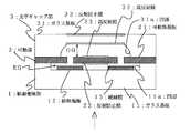
図1は、本発明の実施の形態における波長可変光フィルタを示す断面図である。なお、図1は、波長可変光フィルタの中央からややずれた位置における断面図である(図2のA−A'参照)。
この実施の形態の波長可変光フィルタは、駆動電極部1と、可動部2と、光学ギャップ部3とから構成されており、駆動電極部1と可動部2との間にはその長さが約4μmの静電ギャップEGが、可動部2と光学ギャップ部3との間にはその長さが約30μmの光学ギャップOGがそれぞれ形成されている。駆動電極部1は、断面略コ字状のガラス基板11の略中央部に形成された凹部11a上に略リング状の駆動電極12及び絶縁膜13が形成されて構成されている。ガラス基板11は、例えば、ナトリウム(Na)やカリウム(K)等のアルカリ金属を含有したガラスからなる。この種のガラスとしては、例えば、アルカリ金属を含有したホウケイ酸ガラス、具体的には、コーニング社製のパイレックス(登録商標)・ガラスがある。ガラス基板11を構成するガラスは、駆動電極部1と可動部2とを陽極接合(後述)により接合する場合には、ガラス基板11を加熱するため、可動部2を構成するシリコンと熱膨張係数がほぼ等しいことが要求されることから、上記パイレックス(登録商標)・ガラスのうち、コーニング#7740(商品名)が好ましい。FIG. 1 is a cross-sectional view showing a wavelength tunable optical filter according to an embodiment of the present invention. 1 is a cross-sectional view at a position slightly deviated from the center of the wavelength tunable optical filter (see AA ′ in FIG. 2).
The wavelength tunable optical filter of this embodiment is composed of a
駆動電極12は、例えば、金(Au)やクロム(Cr)等の金属、あるいは透明導電性材料からなる。透明導電性材料としては、例えば、酸化錫(SnO2)、酸化インジウム(In2O3)、あるいは錫ドープ酸化インジウム(ITO:Indium Tin Oxide)等がある。また、駆動電極12の膜厚は、例えば、0.1〜0.2μmである。なお、駆動電極12は、図示しないが、ガラス基板11の外部に設けられた端子に配線を介して接続されている。絶縁膜13は、例えば、二酸化シリコン(SiO2)又は窒化シリコン(SiNx)からなり、駆動電極12と後述する可動体21aとのスティッキングを防止するために形成されている。The drive electrode 12 is made of, for example, a metal such as gold (Au) or chromium (Cr), or a transparent conductive material. Examples of the transparent conductive material include tin oxide (SnO2 ), indium oxide (In2 O3 ), and tin-doped indium oxide (ITO). Moreover, the film thickness of the drive electrode 12 is 0.1-0.2 micrometer, for example. Although not shown, the drive electrode 12 is connected to a terminal provided outside the
可動部2は、可動部基板21と、反射防止膜22と、高反射膜23とから構成されている。可動部基板21は、例えば、二酸化シリコン(SiO2)からなり、約4μmの膜厚を有し、図2に示すように、可動体21aと、4個のヒンジ21bと、支持部21cとが一体に形成されて構成されている。可動体21aは、略円盤状であり、可動部基板21の略中央に形成されている。可動体21は、その周縁部に形成された4個のヒンジ21bを介して支持部21cに支持され、自在に上下動する。4個のヒンジ21bは、可動体21aの周縁に、隣接するもの同士が約90度の角度をなして位置している。The
反射防止膜22は、可動体21aの下面のほぼ全域に略円盤状に形成され、二酸化シリコン(SiO2)の薄膜と五酸化タンタル(Ta2O5)の薄膜とを交互に積層した多層膜からなる。反射防止膜22は、図1において駆動電極部1の略中央下方(図1の矢印参照)から入射された光が図中下方に反射されるのを防止するとともに、一旦反射防止膜22の上方に透過された後高反射膜23で反射された光が図中上方に再度反射されるのを防止する。高反射膜23は、可動体21aの上面のほぼ全域に略円盤状に形成され、二酸化シリコン(SiO2)の薄膜と五酸化タンタル(Ta2O5)の薄膜とを交互に積層した多層膜からなる。高反射膜23は、図1において駆動電極部1の略中央下方(図1の矢印参照)から入射され、一旦その上方に透過された光を、光学ギャップ部3を構成するガラス基板31の下面に形成された高反射膜32との間で複数回にわたって反射させるためのものである。反射防止膜22及び高反射膜23は、二酸化シリコン(SiO2)の薄膜及び五酸化タンタル(Ta2O5)の薄膜の各膜厚を変更することにより形成される。The
光学ギャップ部3は、ガラス基板31と、高反射膜32と、反射防止膜33とから構成されている。ガラス基板31は、ガラス基板11と同一の材質のガラスからなり、その略中央部に凹部31aが形成された断面略両持ち梁状である。高反射膜32は、光学ギャップ部3の凹部31aの下面に略円盤状に形成され、二酸化シリコン(SiO2)の薄膜と五酸化タンタル(Ta2O5)の薄膜とを交互に積層した多層膜からなる。高反射膜32は、図1において可動部2の略中央下方から入射され、一旦その上方に透過された光を、可動部2を構成する高反射膜23との間で複数回にわたって反射させるためのものである。反射防止膜33は、光学ギャップ部3の略中央上面に略円盤状に形成され、二酸化シリコン(SiO2)の薄膜と五酸化タンタル(Ta2O5)の薄膜とを交互に積層した多層膜からなる。反射防止膜33は、図1において光学ギャップ部3を構成するガラス基板31を透過した光が図中下方に反射されるのを防止する。高反射膜32及び反射防止膜33は、二酸化シリコン(SiO2)の薄膜及び五酸化タンタル(Ta2O5)の薄膜の各膜厚を変更することにより形成される。The
次に、上記構成の波長可変光フィルタの製造方法について、図3〜図8を参照して説明する。まず、駆動電極部1を製造するために、コーニング#7740のパイレックス(登録商標)・ガラスからなるガラス基板14(図3(1)参照)の上面に、図3(2)に示すように、化学的蒸着(CVD:Chemical Vapor Deposition)装置や物理的蒸着(PVD:Physical Vapor Deposition)装置を使用して、金(Au)やクロム(Cr)等の金属膜15を形成する。PVD装置としては、例えば、スパッタリング装置、真空蒸着装置、あるいはイオンプレーティング装置等がある。金属膜15の膜厚は、例えば、0.1μmとする。具体的には、クロム(Cr)膜の場合にはその膜厚を0.1μmとすれば良いが、金(Au)膜の場合にはガラス基板14との密着性が良好でないことから、膜厚が例えば0.03μmであるクロム(Cr)膜を形成した後、膜厚が例えば0.07μmである金(Au)膜を形成する。 Next, a manufacturing method of the wavelength tunable optical filter having the above configuration will be described with reference to FIGS. First, in order to manufacture the
次に、金属膜15の上面全面にフォトレジスト(図示略)を塗布し、マスクアライナーで金属膜15の上面全面に塗布されたフォトレジストを露光した後、現像液で現像するフォトリソグラフィ(photolithography)技術を使用して、ガラス基板14のうち、後にガラス基板11の凹部11a(図1参照)となる部分を形成するために、フォトレジストパターン(図示略)を形成する。次に、ウエットエッチング技術を使用して、例えば、塩酸又は硫酸(クロム膜の場合)、あるいは王水又は酸素や水の存在下でシアン化物イオンを含む溶液(金膜の場合)(以下、金属エッチング液と呼ぶ。)により金属膜15のうち不要な部分を除去した後、図示せぬフォトレジストパターンを除去して、図3(3)に示すエッチングパターン16を得る。 Next, a photoresist (not shown) is applied to the entire upper surface of the metal film 15, and the photoresist applied to the entire upper surface of the metal film 15 is exposed with a mask aligner, and then developed with a developer. Using a technique, a photoresist pattern (not shown) is formed to form a portion of the glass substrate 14 that will later become a recess 11a (see FIG. 1) of the
次に、ウエットエッチング技術を使用して、例えば、フッ化水素酸(HF)によりガラス基板14のうち不要な部分を除去して図3(4)に示す凹部11aを形成した後、ウエットエッチング技術を使用して、上記した金属エッチング液によりエッチングパターン16を除去して、図3(5)に示すように、約4μmの深さを有する凹部11aが形成されたガラス基板11を得る。次に、ガラス基板11の上面に、図3(6)に示すように、CVD装置やPVD装置を使用して、金(Au)やクロム(Cr)等の金属膜17を形成する。金属膜17の膜厚は、例えば、0.1〜0.2μmとする。次に、金属膜17の上面全面にフォトレジスト(図示略)を塗布した後、上記したフォトリソグラフィ技術を使用して、金属膜17のうち、後に駆動電極12となる部分を残すために、フォトレジストパターン(図示略)を形成する。次に、ウエットエッチング技術を使用して、上記した金属エッチング液により金属膜17のうち不要な部分を除去した後、図示せぬフォトレジストパターンを除去して、図4(1)に示すように、駆動電極12を得る。次に、CVD装置を使用して、図4(2)に示すように、駆動電極12上に二酸化シリコン(SiO2)又は窒化シリコン(SiNx)からなる絶縁膜13を形成する。以上説明した製造工程により、図1に示す駆動電極部1が製造される。Next, using a wet etching technique, for example, unnecessary portions of the glass substrate 14 are removed by hydrofluoric acid (HF) to form the recesses 11a shown in FIG. Then, the etching pattern 16 is removed with the above-described metal etching solution to obtain a
次に、可動部2を製造するために、図5(1)に示すSOI基板24を用いる。SOI基板24は、ベース層25と、絶縁層26と、活性層27とから構成されている。ベース層25は、シリコン(Si)からなり、その膜厚は例えば、500μmである。絶縁層26は、二酸化シリコン(SiO2)からなり、その膜厚は例えば、4μmである。活性層27はシリコン(Si)からなり、その膜厚は例えば、10μmである。活性層27の上面の略中央部に、CVD装置やPVD装置を使用して、二酸化シリコン(SiO2)の薄膜と五酸化タンタル(Ta2O5)の薄膜とを交互に、例えば、10〜20層程度積層することにより、図5(2)に示す反射防止膜22を形成する。Next, in order to manufacture the
次に、図4(2)に示す駆動電極部1と、図5(2)に示す反射防止膜22が形成されたSOI基板24とを、略円盤状の反射防止膜22が略リング状の駆動電極12のリング部分に対向するように接合する。この接合には、例えば、陽極接合、接着剤による接合、表面活性化接合、低融点ガラスを用いた接合を用いる。このうち、陽極接合は、以下に示す工程を経て行われる。まず、駆動電極部1の上面に、反射防止膜22が形成されたSOI基板24を、反射防止膜22が駆動電極12のリング部分に対向するように載置した状態において、図示せぬ直流電源のマイナス端子をガラス基板11に接続するとともに、上記直流電源のプラス端子を活性層27に接続する。次に、ガラス基板11を例えば、数百℃程度に加熱しつつ、ガラス基板11と活性層27との間に直流電圧を例えば、数百V程度印加する。ガラス基板11を加熱することにより、ガラス基板11内のアルカリ金属のプラスイオン、例えば、ナトリウムイオン(Na+)が移動しやすくなる。このアルカリ金属のプラスイオンがガラス基板11内を移動することにより、相対的に、ガラス基板11の活性層27との接合面がマイナスに帯電する一方、活性層27のガラス基板11との接合面がプラスに帯電する。この結果、シリコン(Si)と酸素(O)とが電子対を共有する共有結合により、図6に示すように、ガラス基板11と活性層27とは強固に接合される。Next, the
次に、図6に示す構造体からベース層25を除去することにより、図7(1)に示す構造体とする。このベース層25の除去には、ウエットエッチング、ドライエッチング、あるいは研磨を用いる。いずれの除去法においても絶縁層26が活性層27に対するエッチングのストッパーの役割を果たすために、駆動電極12に対向している活性層27がダメージを受けず、歩留まりの高い波長可変光フィルタを製造することができる。以下、ウエットエッチング除去法及びドライエッチング除去法について説明する。なお、研磨除去法については、半導体製造分野において用いられている周知の研磨除去法を用いることができるので、その説明を省略する。 Next, the
(1)ウエットエッチング除去法
図6に示す構造体を例えば、1〜40重量%(好ましくは、10重量%前後)の濃度の水酸化カリウム(KOH)水溶液に浸漬することにより、式(2)に示す反応式に基づいてベース層25を構成するシリコン(Si)がエッチングされる。
Si+2KOH+H2O→K2SiO3+2H2 ・・・(2)
この場合のシリコン(Si)のエッチングレートは、二酸化シリコン(SiO2)のエッチングレートよりも非常に大きいので、二酸化シリコン(SiO2)からなる絶縁層26がシリコン(Si)からなる活性層27に対するエッチングのストッパーの役割を果たす。(1) Wet Etching Removal Method The structure shown in FIG. 6 is immersed in an aqueous potassium hydroxide (KOH) solution having a concentration of 1 to 40% by weight (preferably around 10% by weight), for example. The silicon (Si) constituting the
Si + 2KOH + H2 O → K2 SiO3 + 2H2 (2)
Since the etching rate of the silicon (Si) in this case is much greater than the etching rate of the silicon dioxide (SiO2), for the
なお、この場合に用いるエッチング液としては、上記した水酸化カリウム(KOH)水溶液の他、半導体表面処理剤やフォトリソグラフィ用のポジレジスト用現像液として広く使用されている水酸化テトラメチルアンモニウム(TMAH:Tetramethyl ammonium hydroxide)水溶液、エチレンジアミン−ピロカテコール−ジアジン(EPD:Ethylenediamine Pyrocatechol Diazine)水溶液又は、ヒドラジン(Hydrazine)水溶液などがある。このウエットエッチング除去法を用いれば、図6に示す構造体の一団を、生産条件等をほぼ等しくして一括して処理するバッチ処理を行うことができるので、生産性を向上させることができる。 The etching solution used in this case includes tetramethylammonium hydroxide (TMAH) widely used as a semiconductor surface treatment agent and a positive resist developer for photolithography in addition to the above-mentioned potassium hydroxide (KOH) aqueous solution. : Tetramethyl ammonium hydroxide) aqueous solution, ethylenediamine-pyrocatechol-diazine (EPD) aqueous solution, hydrazine (Hydrazine) aqueous solution, or the like. If this wet etching removal method is used, a batch process in which a group of structures shown in FIG. 6 is collectively processed under substantially the same production conditions and the like can be performed, so that productivity can be improved.
(2)ドライエッチング除去法
図6に示す構造体をドライエッチング装置のチャンバー内に載置し、真空状態にした後、チャンバー内に例えば、圧力390Paの二フッ化キセノン(XeF2)を60秒間導入することにより、式(3)に示す反応式に基づいてベース層25を構成するシリコン(Si)がエッチングされる。
2XeF2+Si→2Xe+SiF4 ・・・(3)
この場合のシリコン(Si)のエッチングレートは、二酸化シリコン(SiO2)のエッチングレートよりも非常に大きいので、二酸化シリコン(SiO2)からなる絶縁層26がシリコン(Si)からなる活性層27に対するエッチングのストッパーの役割を果たす。また、この場合のドライエッチングは、プラズマエッチングではないので、ガラス基板11や絶縁層26がダメージを受けにくい。なお、上記した二フッ化キセノン(XeF2)を用いたドライエッチングの他、四フッ化炭素(CF4)や六フッ化硫黄(SF6)を用いたプラズマエッチングがある。(2) Dry Etching Removal Method After the structure shown in FIG. 6 is placed in a chamber of a dry etching apparatus and evacuated, for example, xenon difluoride (XeF2 ) at a pressure of 390 Pa is placed in the chamber for 60 seconds. By introducing, silicon (Si) constituting the
2XeF2 + Si → 2Xe + SiF4 (3)
Since the etching rate of the silicon (Si) in this case is much greater than the etching rate of the silicon dioxide (SiO2), for the
次に、図7(1)に示す構造体について、ウエットエッチング技術を使用して、例えば、フッ化水素酸(HF)により、図7(2)に示すように、絶縁層26をすべて除去する。次に、活性層27の上面全面にフォトレジスト(図示略)を塗布した後、上記したフォトリソグラフィ技術を使用して、活性層27のうち、後に可動部基板21となる部分を残すために、フォトレジストパターン(図示略)を形成する。次に、図7(2)に示す構造体に図示せぬフォトレジストパターンが形成されたものをドライエッチング装置のチャンバー内に載置した後、例えば、エッチングガスとして六フッ化硫黄(SF6)を流量130sccmで6秒間、デポジション(堆積)ガスとして八フッ化シクロブタン(C4F8)を流量50sccmで7秒間交互にチャンバー内に導入することにより、活性層27のうち不要な部分を異方性エッチングで除去する。ここで、ドライエッチング技術を使用して異方性エッチングを行うのは、以下に示す理由による。まず、ウェットエッチング技術を使用した場合、エッチングが進むに従ってエッチング液が可動部基板21に形成された孔から下方の駆動電極部1側に侵入し、駆動電極12や絶縁膜13を除去してしまうが、ドライエッチング技術を使用した場合はそのような危険性がない。また、等方性エッチングを使用した場合には、活性層27が等方的にエッチングされ、サイドエッチングが発生する。特に、ヒンジ21bにサイドエッチングが発生した場合には、強度が弱くなり、耐久性が劣化してしまう。これに対し、異方性エッチングを使用した場合には、サイドエッチングが発生せず、エッチング寸法の制御に優れており、ヒンジ21bの側面も垂直に形成されるため、強度が弱くなることはない。Next, as shown in FIG. 7 (2), the insulating
次に、上記異方性エッチング後の構造体について、図示せぬフォトレジストパターンを、例えば、酸素プラズマを使用して除去して、図7(3)に示すように、可動部基板21を得る。ここで、酸素プラズマを使用して図示せぬフォトレジストパターンを除去するのは、以下に示す理由による。すなわち、剥離液や硫酸その他の酸性の溶液を用いて図示せぬフォトレジストパターンを除去した場合、剥離液や酸性の溶液が可動部基板21に形成された孔から下方の駆動電極部1側に侵入し、駆動電極12や絶縁膜13を除去してしまうが、酸素プラズマを使用した場合はそのような危険性がないからである。 Next, the photoresist pattern (not shown) is removed from the structure after the anisotropic etching by using, for example, oxygen plasma to obtain the
次に、可動部基板21の上面の略中央部に、CVD装置やPVD装置を使用して、二酸化シリコン(SiO2)の薄膜と五酸化タンタル(Ta2O5)の薄膜とを交互に、例えば、10〜20層程度積層することにより、図7(4)に示す高反射膜23を形成する。以上説明した製造工程により、図1に示す可動部2が製造される。Next, a thin film of silicon dioxide (SiO2 ) and a thin film of tantalum pentoxide (Ta2 O5 ) are alternately used in a substantially central portion of the upper surface of the
次に、光学ギャップ部3を製造するために、コーニング7740のパイレックス(登録商標)・ガラスからなるガラス基板34(図8(1)参照)の上面に、図8(2)に示すように、CVD装置やPVD装置を使用して、金(Au)やクロム(Cr)等の金属膜35を形成する。金属膜35として金(Au)を用いた場合、その膜厚は例えば、0.07μm、金属膜35としてクロム(Cr)を用いた場合、その膜厚は例えば、0.03μmとする。 Next, in order to manufacture the
次に、金属膜35の上面全面にフォトレジスト(図示略)を塗布し、上記したフォトリソグラフィ技術を使用して、ガラス基板34のうち、後にガラス基板31の凹部31a(図1参照)となる部分を形成するために、フォトレジストパターン(図示略)を形成する。次に、ウエットエッチング技術を使用して、上記した金属エッチング液により金属膜35のうち不要な部分を除去した後、図示せぬフォトレジストパターンを除去して、図8(3)に示すエッチングパターン36を得る。 Next, a photoresist (not shown) is applied to the entire upper surface of the metal film 35, and the recesses 31a (see FIG. 1) of the
次に、ウエットエッチング技術を使用して、例えば、フッ化水素酸(HF)によりガラス基板34のうち不要な部分を除去して図8(4)に示す凹部31aを形成した後、ウエットエッチング技術を使用して、上記した金属エッチング液によりエッチングパターン36を除去して、図8(5)に示すように、凹部31aが形成されたガラス基板31を得る。なお、ガラス基板31が図8(5)に示すように、断面略両持ち梁状となるのは、フッ化水素酸(HF)により等方的にエッチングされるためである。次に、ガラス基板31の凹部31aの上面及び略中央下面に、CVD装置やPVD装置を使用して、二酸化シリコン(SiO2)の薄膜と五酸化タンタル(Ta2O5)の薄膜とを交互に、例えば、10〜20層程度積層することにより、図8(6)に示す高反射膜32及び反射防止膜33を形成する。以上説明した製造工程により、図1に示す光学ギャップ部3が製造される。Next, using wet etching technology, for example, unnecessary portions of the glass substrate 34 are removed by hydrofluoric acid (HF) to form the recesses 31a shown in FIG. 8 (4), and then wet etching technology is used. Then, the etching pattern 36 is removed with the above-described metal etching solution to obtain the
次に、図7(4)に示す構造体と、図8(6)に示す光学ギャップ部3とを、略円盤状の高反射膜23が略円盤状の高反射膜32に対向するように接合する。この接合には、例えば、上記した陽極接合、接着剤による接合、表面活性化接合、低融点ガラスを用いた接合を用いる。この接合の際、内部を真空にしたり(真空封止)、内部を最適圧力として(減圧封止)も良い。以上説明した製造工程により、図1に示す波長可変光フィルタが製造される。 Next, the structure shown in FIG. 7 (4) and the
次に、上記構成の波長可変光フィルタの動作について、図1を参照して説明する。駆動電極12と可動体21aとの間には駆動電圧を印加する。この駆動電圧は、例えば、60Hzの交流正弦波電圧やパルス状の電圧であり、駆動電極12にはガラス基板11の外部に設けられた端子及び配線(ともに図示略)を介して印加する一方、可動体21aには支持部21c及びヒンジ21b(図2参照)を介して印加する。この駆動電圧による電位差のため、駆動電極12と可動体21aとの間に静電引力が発生し、可動体21aが駆動電極12側に変位する、すなわち、静電ギャップEG及び光学ギャップOGが変化する。このとき、ヒンジ21bが弾性を有しているため、可動体21aは弾性的に変位する。 Next, the operation of the wavelength tunable optical filter having the above configuration will be described with reference to FIG. A drive voltage is applied between the drive electrode 12 and the movable body 21a. This drive voltage is, for example, an alternating sine wave voltage of 60 Hz or a pulse voltage, and is applied to the drive electrode 12 via terminals and wiring (both not shown) provided outside the
この波長可変光フィルタに、複数(例えば、60〜100個)の赤外の波長を有する光が図1において駆動電極部1の略中央下方(図1の矢印参照)から入射し、ガラス基板11を透過する。この光は、反射防止膜22によりほとんど反射されず、かつ、シリコンからなる可動体21aを透過して、下方に高反射膜21が、上方に高反射膜32がそれぞれ形成された空間(反射空間)に進入する。上記反射空間に進入した光は、高反射膜23と高反射膜32との間で反射を繰り返し、最終的に高反射膜32及びガラス基板31を透過してこの波長可変光フィルタの上方から出射する。このとき、ガラス基板31の上面に反射防止膜33が形成されているため、光がガラス基板31と空気の界面でほとんど反射されずに出射する。 Light having a plurality of (for example, 60 to 100) infrared wavelengths is incident on the wavelength tunable optical filter from substantially below the center of the drive electrode unit 1 (see the arrow in FIG. 1) in FIG. Transparent. This light is hardly reflected by the
上記の高反射膜32(固定鏡)と高反射膜23(可動鏡)との間で光が反射を繰り返す過程において、高反射膜32と高反射膜23との間の距離(光学ギャップOG)に対応する干渉条件を満たさない波長の光は急激に減衰し、この干渉条件を満たした波長の光だけが残って最終的にこの波長可変光フィルタから出射する。これがファブリ・ペロー干渉計の原理であり、この干渉条件を満たした波長の光が透過することとなるため、駆動電圧を変更することにより、可動体21aが変位して光学ギャップOGが変更されると、透過する光の波長を選択することが可能となる。 In the process where light is repeatedly reflected between the high reflection film 32 (fixed mirror) and the high reflection film 23 (movable mirror), the distance between the high reflection film 32 and the high reflection film 23 (optical gap OG). The light having a wavelength that does not satisfy the interference condition corresponding to is rapidly attenuated, and only the light having the wavelength satisfying the interference condition remains and is finally emitted from the wavelength tunable optical filter. This is the principle of the Fabry-Perot interferometer, and light having a wavelength satisfying this interference condition is transmitted. Therefore, by changing the drive voltage, the movable body 21a is displaced and the optical gap OG is changed. Then, it becomes possible to select the wavelength of the transmitted light.
このように、この実施の形態による波長可変光フィルタは、ガラス基板11を有する駆動電極部1と、シリコン(Si)からなる可動部2と、ガラス基板31を有する光学ギャップ部3とを接合して構成されているので、静電ギャップEGが高精度で形成される。特に、陽極接合を用いた場合には、極めて高精度で静電ギャップEGが形成される。したがって、可動体21aと駆動電極12との間に、ある駆動電圧を印加すれば、設計時にその駆動電圧に対して想定した静電引力を発生させることができ、設計通りに可動体21aを変位させることができる。この結果、各波長可変光フィルタごとに、各波長を有する光を取り出すための駆動電圧を調整して設定する必要がないため、使い勝手が良く、また光ファイバ中を伝送される異なる波長を有するすべての光を取り出すことができる。 As described above, the wavelength tunable optical filter according to this embodiment joins the
また、この実施の形態による波長可変光フィルタでは、犠牲層を形成することなく、静電ギャップEGが形成されているとともに、駆動電極12上に絶縁膜13が形成されている。したがって、たとえ静電ギャップEGの長さを短く形成したとしても、上記した第1及び第2の従来例とは異なり、製造時及び使用時のいずれの場合にも、スティッキングを防止することができる。この結果、歩留まり及び耐久性を向上させることができる。さらに、この実施の形態による波長可変光フィルタでは、製造過程で犠牲層が形成されないため、その犠牲層を除去するためのリリースホールを可動部基板21等に形成する必要がなく、その分設計通りの面積を有する可動体21aが得られる。したがって、上記した第1及び第2の従来例と比べて、低い駆動電圧で駆動することができ、その分消費電力を削減することができる。 In the wavelength tunable optical filter according to this embodiment, the electrostatic gap EG is formed without forming the sacrificial layer, and the insulating
また、この実施の形態による波長可変光フィルタでは、ガラス基板34に高精度のガラスエッチングを施すことにより凹部31aを形成するとともに、光学ギャップ部3と可動部2とを接合、特に、陽極接合しているので、光学ギャップOGも高精度に形成することができる。このため、波長可変光フィルタを安定的に駆動することができる。さらに、この実施の形態による波長可変光フィルタでは、透明なガラス基板31が封止キャップをも兼ねているので、波長可変光フィルタの動作をモニタすることができる。 Further, in the wavelength tunable optical filter according to this embodiment, the glass substrate 34 is subjected to high-precision glass etching to form the concave portion 31a, and the
また、この実施の形態による波長可変光フィルタでは、SOI基板24から可動部2を形成しているので、高精度な膜厚を有する可動体21aを形成することができる。また、SOI基板24として、一般に市販されているものを用いた場合には、既にその製造メーカによって活性層27の表面が鏡面に仕上げられているので、それを利用して高精度な反射防止膜22及び高反射膜23を形成することができる。 In the wavelength tunable optical filter according to this embodiment, since the
以上、この実施の形態を図面を参照して詳述してきたが、具体的な構成はこの実施の形態に限られるものではなく、本発明の要旨を逸脱しない範囲の設計の変更等があっても本発明に含まれる。
例えば、上述の実施の形態においては、可動部2を製造するのにSOI基板24を用いる例を示したが、これに限定されず、SOS(Silicon on Sapphire)基板を用いてもよく、またその上面に二酸化シリコン(SiO2)膜が形成されたシリコン基板と、他のシリコン基板とを上面同士を重ねて張り合わせたものを用いても良い。
また、上述の実施の形態においては、駆動電極部1及び光学ギャップ部3の両方をガラス基板で構成する例を示したが、これに限定されず、駆動電極部1及び光学ギャップ部3は、赤外等の所望の透過波長帯域の光を透過する材料、例えば、シリコン、サファイヤ、ゲルマニウムなどでも良い。The embodiment has been described in detail with reference to the drawings. However, the specific configuration is not limited to the embodiment, and there are design changes and the like without departing from the scope of the invention. Are also included in the present invention.
For example, in the above-described embodiment, the example in which the
Moreover, in the above-mentioned embodiment, although the example which comprises both the
また、上述の実施の形態においては、ヒンジ21bは4個である例を示したが、これに限定されず、ヒンジの数は、3個、5個、6個以上でも良い。この場合、隣接するヒンジは、可動体21aの周辺部に等距離となる位置に形成する。また、上述の実施の形態においては、駆動電極部1と図5(2)に示す構造体を接合した後に可動部2を形成し、その後図7(4)に示す構造体と光学ギャップ部3とを接合する例を示したが、これに限定されない。例えば、まず、光学ギャップ部3と活性層27に高反射膜23が形成されたSOI基板24とを接合した後に可動部2を形成し、その後これらと駆動電極部1とを接合しても良い。このように、この実施の形態による波長可変光フィルタは、製造工程に自由度がある。 Further, in the above-described embodiment, an example in which the number of
また、上述の実施の形態においては、駆動電極12上に絶縁膜13を形成する例を示したが、これに限定されず、可動体21aの下面であって、少なくとも駆動電極12に対向した領域に絶縁膜を形成しても良い。この絶縁膜の形成方法としては、例えば、シリコンを酸化性雰囲気中で加熱する熱酸化や、TEOS(Tetra Ethyl Ortho Silicate)−CVD装置を使用して、それぞれ二酸化シリコン(SiO2)膜を形成する。また、可動体21aの略中央下面に形成される反射防止膜22を構成する二酸化シリコン(SiO2)膜も五酸化タンタル(Ta2O5)膜もともに絶縁体である。そこで、反射防止膜22を可動体21aの下面全面に形成して、上記した絶縁膜として兼用しても良い。この場合、可動体21aの下面の周辺部については、反射防止膜22として機能するだけの層数を形成する必要はなく、絶縁膜として機能するだけの層数形成すれば良い。さらに、上記絶縁膜13と、可動体21aの下面に形成する絶縁膜との両方を形成しても良い。このように、反射防止膜22を絶縁膜として兼用すれば、少ない製造工程で上述の実施の形態と同様の効果を得ることができ、安価に波長可変光フィルタを構成することができる。また、上述の実施の形態においては、光学ギャップ部3の下面全面に高反射膜32を形成する例を示したが、これに限定されず、高反射膜32は、光学ギャップ部3の下面のうち、高反射膜23に対向した領域だけに形成しても良い。In the above-described embodiment, the example in which the insulating
1 駆動電極部、2 可動部、3 光学ギャップ部、11,14,31,34 ガラス基板、11a,31a 凹部、12 駆動電極、13 絶縁膜、15,17,35 金属膜、16,36 エッチングパターン、21 可動部基板、21a 可動体、21b ヒンジ、21c 支持部、22,33 反射防止膜、23,32 高反射膜、24 SOI基板、25 ベース層、26 絶縁層、27 活性層、EG 静電ギャップ、OG 光学ギャップ。
DESCRIPTION OF
Claims (11)
Translated fromJapanese前記可動体と所定の静電ギャップを隔てて対向した駆動電極が形成された駆動電極部と、
前記可動鏡と所定の光学ギャップを隔てて対向した固定鏡が形成された光学ギャップ部とが互いに接合され、
前記駆動電極の前記可動体に対向した領域と、前記可動体の前記駆動電極に対向した領域とのいずれか一方又は両方に絶縁膜が形成されていることを特徴とする波長可変光フィルタ。A movable mirror is formed on one surface and supports a movable body that moves freely up and down;
A drive electrode portion on which a drive electrode facing the movable body with a predetermined electrostatic gap is formed;
The movable mirror and an optical gap part formed with a fixed mirror facing each other with a predetermined optical gap are joined together,
A wavelength tunable optical filter, wherein an insulating film is formed in one or both of a region of the drive electrode facing the movable body and a region of the movable body facing the drive electrode.
第2の基板に第2の凹部を形成した後、前記第2の凹部に固定鏡を形成して光学ギャップ部とする第2の工程と、
導電性を有する活性層、絶縁層及びベース層が順次積層された第3の基板と前記駆動電極部とを、前記駆動電極と前記活性層とを対向させて接合した後、前記ベース層及び前記絶縁層を順次除去し、前記活性層に可動体を形成した後、前記可動体に可動鏡を形成する第3の工程と、
前記第3の工程で製造された構造体と前記光学ギャップ部とを、前記可動鏡と前記固定鏡とを対向させて接合する第4の工程と
を有することを特徴とする波長可変光フィルタの製造方法。A first step of forming a first recess in the first substrate and then forming a drive electrode in the first recess to form a drive electrode portion;
A second step of forming a second recess in the second substrate and then forming a fixed mirror in the second recess to form an optical gap portion;
After the conductive substrate, the drive electrode unit, and the third substrate on which the conductive active layer, the insulating layer, and the base layer are sequentially stacked are joined with the drive electrode facing the active layer, the base layer and the base layer A third step of sequentially removing the insulating layer, forming a movable body on the active layer, and then forming a movable mirror on the movable body;
And a fourth step of joining the structure manufactured in the third step and the optical gap portion with the movable mirror and the fixed mirror facing each other. Production method.
第2の基板に第2の凹部を形成した後、前記第2の凹部に固定鏡を形成して光学ギャップ部とする第2の工程と、
導電性を有し可動鏡が形成された活性層、絶縁層及びベース層が順次積層された第3の基板と前記光学ギャップ部とを、前記可動鏡と前記固定鏡とを対向させて接合した後、前記ベース層及び前記絶縁層を順次除去し、前記活性層に可動体を形成する第3の工程と、
前記第3の工程で製造された構造体と前記駆動電極部とを、前記可動体と前記駆動電極とを対向させて接合する第4の工程と
を有することを特徴とする波長可変光フィルタの製造方法。A first step of forming a first recess in the first substrate and then forming a drive electrode in the first recess to form a drive electrode portion;
A second step of forming a second recess in the second substrate and then forming a fixed mirror in the second recess to form an optical gap portion;
A third substrate on which an active layer, an insulating layer, and a base layer, which are electrically conductive and have a movable mirror formed thereon, and the optical gap portion are joined with the movable mirror and the fixed mirror facing each other. A third step of sequentially removing the base layer and the insulating layer to form a movable body in the active layer;
And a fourth step of joining the structure manufactured in the third step and the drive electrode portion with the movable body and the drive electrode facing each other. Production method.
Priority Applications (5)
| Application Number | Priority Date | Filing Date | Title |
|---|---|---|---|
| JP2003291165AJP3786106B2 (en) | 2003-08-11 | 2003-08-11 | Wavelength tunable optical filter and manufacturing method thereof |
| CNB2004100563455ACN1289926C (en) | 2003-08-11 | 2004-08-06 | Wavelength-variable filter and its making method |
| US10/915,122US20050068627A1 (en) | 2003-08-11 | 2004-08-10 | Tunable optical filter and method of manufacturing same |
| TW093123941ATWI248525B (en) | 2003-08-11 | 2004-08-10 | Wavelength-tunable filter and method of manufacturing the same |
| KR1020040062669AKR100659812B1 (en) | 2003-08-11 | 2004-08-10 | Tunable optical filter and method of manufacturing same |
Applications Claiming Priority (1)
| Application Number | Priority Date | Filing Date | Title |
|---|---|---|---|
| JP2003291165AJP3786106B2 (en) | 2003-08-11 | 2003-08-11 | Wavelength tunable optical filter and manufacturing method thereof |
Publications (2)
| Publication Number | Publication Date |
|---|---|
| JP2005062384A JP2005062384A (en) | 2005-03-10 |
| JP3786106B2true JP3786106B2 (en) | 2006-06-14 |
Family
ID=34368932
Family Applications (1)
| Application Number | Title | Priority Date | Filing Date |
|---|---|---|---|
| JP2003291165AExpired - Fee RelatedJP3786106B2 (en) | 2003-08-11 | 2003-08-11 | Wavelength tunable optical filter and manufacturing method thereof |
Country Status (5)
| Country | Link |
|---|---|
| US (1) | US20050068627A1 (en) |
| JP (1) | JP3786106B2 (en) |
| KR (1) | KR100659812B1 (en) |
| CN (1) | CN1289926C (en) |
| TW (1) | TWI248525B (en) |
Cited By (3)
| Publication number | Priority date | Publication date | Assignee | Title |
|---|---|---|---|---|
| US8970957B2 (en) | 2011-02-17 | 2015-03-03 | Seiko Epson Corporation | Tunable interference filter, optical module, and electronic device |
| US9372293B2 (en) | 2012-08-30 | 2016-06-21 | Seiko Espon Corporation | Variable wavelength interference filter, optical module, electronic apparatus, and method of manufacturing variable wavelength interference filter |
| US9658446B2 (en) | 2013-03-18 | 2017-05-23 | Seiko Epson Corporation | Sealing structure, interference filter, optical module, and electronic apparatus |
Families Citing this family (75)
| Publication number | Priority date | Publication date | Assignee | Title |
|---|---|---|---|---|
| JP3770326B2 (en)* | 2003-10-01 | 2006-04-26 | セイコーエプソン株式会社 | Analysis equipment |
| US8008736B2 (en) | 2004-09-27 | 2011-08-30 | Qualcomm Mems Technologies, Inc. | Analog interferometric modulator device |
| US7420725B2 (en) | 2004-09-27 | 2008-09-02 | Idc, Llc | Device having a conductive light absorbing mask and method for fabricating same |
| US7304784B2 (en)* | 2004-09-27 | 2007-12-04 | Idc, Llc | Reflective display device having viewable display on both sides |
| US7564612B2 (en)* | 2004-09-27 | 2009-07-21 | Idc, Llc | Photonic MEMS and structures |
| US7527995B2 (en)* | 2004-09-27 | 2009-05-05 | Qualcomm Mems Technologies, Inc. | Method of making prestructure for MEMS systems |
| US7289259B2 (en) | 2004-09-27 | 2007-10-30 | Idc, Llc | Conductive bus structure for interferometric modulator array |
| US7936497B2 (en) | 2004-09-27 | 2011-05-03 | Qualcomm Mems Technologies, Inc. | MEMS device having deformable membrane characterized by mechanical persistence |
| US7630119B2 (en)* | 2004-09-27 | 2009-12-08 | Qualcomm Mems Technologies, Inc. | Apparatus and method for reducing slippage between structures in an interferometric modulator |
| US7583429B2 (en) | 2004-09-27 | 2009-09-01 | Idc, Llc | Ornamental display device |
| US7944599B2 (en)* | 2004-09-27 | 2011-05-17 | Qualcomm Mems Technologies, Inc. | Electromechanical device with optical function separated from mechanical and electrical function |
| US7130104B2 (en)* | 2004-09-27 | 2006-10-31 | Idc, Llc | Methods and devices for inhibiting tilting of a mirror in an interferometric modulator |
| US7302157B2 (en)* | 2004-09-27 | 2007-11-27 | Idc, Llc | System and method for multi-level brightness in interferometric modulation |
| US7372613B2 (en)* | 2004-09-27 | 2008-05-13 | Idc, Llc | Method and device for multistate interferometric light modulation |
| US7884989B2 (en)* | 2005-05-27 | 2011-02-08 | Qualcomm Mems Technologies, Inc. | White interferometric modulators and methods for forming the same |
| US7253083B2 (en)* | 2005-06-17 | 2007-08-07 | Northrop Grumman Corporation | Method of thinning a semiconductor structure |
| US7916980B2 (en) | 2006-01-13 | 2011-03-29 | Qualcomm Mems Technologies, Inc. | Interconnect structure for MEMS device |
| US7550810B2 (en)* | 2006-02-23 | 2009-06-23 | Qualcomm Mems Technologies, Inc. | MEMS device having a layer movable at asymmetric rates |
| US20070242358A1 (en)* | 2006-04-18 | 2007-10-18 | Xerox Corporation | Fabry-perot tunable filter |
| US7628493B2 (en)* | 2006-04-18 | 2009-12-08 | Xerox Corporation | Projector based on tunable individually-addressable Fabry-Perot filters |
| US7649671B2 (en)* | 2006-06-01 | 2010-01-19 | Qualcomm Mems Technologies, Inc. | Analog interferometric modulator device with electrostatic actuation and release |
| US7835061B2 (en) | 2006-06-28 | 2010-11-16 | Qualcomm Mems Technologies, Inc. | Support structures for free-standing electromechanical devices |
| US7527998B2 (en)* | 2006-06-30 | 2009-05-05 | Qualcomm Mems Technologies, Inc. | Method of manufacturing MEMS devices providing air gap control |
| US8115987B2 (en)* | 2007-02-01 | 2012-02-14 | Qualcomm Mems Technologies, Inc. | Modulating the intensity of light from an interferometric reflector |
| KR20090125087A (en)* | 2007-02-20 | 2009-12-03 | 퀄컴 엠이엠스 테크놀로지스, 인크. | Etching Apparatus and Etching Method of Microelectromechanical System MEMS |
| US7742220B2 (en)* | 2007-03-28 | 2010-06-22 | Qualcomm Mems Technologies, Inc. | Microelectromechanical device and method utilizing conducting layers separated by stops |
| US7643202B2 (en)* | 2007-05-09 | 2010-01-05 | Qualcomm Mems Technologies, Inc. | Microelectromechanical system having a dielectric movable membrane and a mirror |
| US7715085B2 (en)* | 2007-05-09 | 2010-05-11 | Qualcomm Mems Technologies, Inc. | Electromechanical system having a dielectric movable membrane and a mirror |
| US7719752B2 (en)* | 2007-05-11 | 2010-05-18 | Qualcomm Mems Technologies, Inc. | MEMS structures, methods of fabricating MEMS components on separate substrates and assembly of same |
| US7782517B2 (en)* | 2007-06-21 | 2010-08-24 | Qualcomm Mems Technologies, Inc. | Infrared and dual mode displays |
| US7630121B2 (en) | 2007-07-02 | 2009-12-08 | Qualcomm Mems Technologies, Inc. | Electromechanical device with optical function separated from mechanical and electrical function |
| EP2183623A1 (en) | 2007-07-31 | 2010-05-12 | Qualcomm Mems Technologies, Inc. | Devices for enhancing colour shift of interferometric modulators |
| US8174698B2 (en)* | 2007-08-10 | 2012-05-08 | Corporation de l'Ecole Polytechnique de Montréal | MEMS tunable silicon fabry-perot cavity and applications thereof |
| JP2011501874A (en)* | 2007-09-14 | 2011-01-13 | クォルコム・メムズ・テクノロジーズ・インコーポレーテッド | Etching process used in MEMS manufacturing |
| US7847999B2 (en) | 2007-09-14 | 2010-12-07 | Qualcomm Mems Technologies, Inc. | Interferometric modulator display devices |
| US7773286B2 (en)* | 2007-09-14 | 2010-08-10 | Qualcomm Mems Technologies, Inc. | Periodic dimple array |
| US20090078316A1 (en)* | 2007-09-24 | 2009-03-26 | Qualcomm Incorporated | Interferometric photovoltaic cell |
| US8058549B2 (en)* | 2007-10-19 | 2011-11-15 | Qualcomm Mems Technologies, Inc. | Photovoltaic devices with integrated color interferometric film stacks |
| CN101828145B (en)* | 2007-10-19 | 2012-03-21 | 高通Mems科技公司 | Displays with integrated photovoltaic elements |
| EP2203765A1 (en)* | 2007-10-23 | 2010-07-07 | Qualcomm Mems Technologies, Inc. | Adjustably transmissive mems-based devices |
| US20090293955A1 (en)* | 2007-11-07 | 2009-12-03 | Qualcomm Incorporated | Photovoltaics with interferometric masks |
| US8941631B2 (en)* | 2007-11-16 | 2015-01-27 | Qualcomm Mems Technologies, Inc. | Simultaneous light collection and illumination on an active display |
| US7715079B2 (en)* | 2007-12-07 | 2010-05-11 | Qualcomm Mems Technologies, Inc. | MEMS devices requiring no mechanical support |
| WO2009085601A2 (en)* | 2007-12-21 | 2009-07-09 | Qualcom Mems Technologies, Inc. | Multijunction photovoltaic cells |
| US8164821B2 (en)* | 2008-02-22 | 2012-04-24 | Qualcomm Mems Technologies, Inc. | Microelectromechanical device with thermal expansion balancing layer or stiffening layer |
| US7944604B2 (en) | 2008-03-07 | 2011-05-17 | Qualcomm Mems Technologies, Inc. | Interferometric modulator in transmission mode |
| US7612933B2 (en)* | 2008-03-27 | 2009-11-03 | Qualcomm Mems Technologies, Inc. | Microelectromechanical device with spacing layer |
| US7898723B2 (en)* | 2008-04-02 | 2011-03-01 | Qualcomm Mems Technologies, Inc. | Microelectromechanical systems display element with photovoltaic structure |
| US7969638B2 (en)* | 2008-04-10 | 2011-06-28 | Qualcomm Mems Technologies, Inc. | Device having thin black mask and method of fabricating the same |
| US8023167B2 (en)* | 2008-06-25 | 2011-09-20 | Qualcomm Mems Technologies, Inc. | Backlight displays |
| US7746539B2 (en)* | 2008-06-25 | 2010-06-29 | Qualcomm Mems Technologies, Inc. | Method for packing a display device and the device obtained thereof |
| US7768690B2 (en)* | 2008-06-25 | 2010-08-03 | Qualcomm Mems Technologies, Inc. | Backlight displays |
| US7859740B2 (en)* | 2008-07-11 | 2010-12-28 | Qualcomm Mems Technologies, Inc. | Stiction mitigation with integrated mech micro-cantilevers through vertical stress gradient control |
| US7855826B2 (en)* | 2008-08-12 | 2010-12-21 | Qualcomm Mems Technologies, Inc. | Method and apparatus to reduce or eliminate stiction and image retention in interferometric modulator devices |
| US8358266B2 (en)* | 2008-09-02 | 2013-01-22 | Qualcomm Mems Technologies, Inc. | Light turning device with prismatic light turning features |
| US20100096011A1 (en)* | 2008-10-16 | 2010-04-22 | Qualcomm Mems Technologies, Inc. | High efficiency interferometric color filters for photovoltaic modules |
| US8270056B2 (en)* | 2009-03-23 | 2012-09-18 | Qualcomm Mems Technologies, Inc. | Display device with openings between sub-pixels and method of making same |
| CN102449512A (en) | 2009-05-29 | 2012-05-09 | 高通Mems科技公司 | Illumination devices and methods of fabrication thereof |
| FI124072B (en)* | 2009-05-29 | 2014-03-14 | Valtion Teknillinen | Micromechanical Fabry-Perot Adjustable Interferometer, Intermediate, and Method of Manufacture |
| US8270062B2 (en)* | 2009-09-17 | 2012-09-18 | Qualcomm Mems Technologies, Inc. | Display device with at least one movable stop element |
| US8488228B2 (en)* | 2009-09-28 | 2013-07-16 | Qualcomm Mems Technologies, Inc. | Interferometric display with interferometric reflector |
| CN101666907B (en)* | 2009-09-29 | 2011-06-01 | 吉林大学 | Electrostatically driven optical waveguide and F-P cavity tunable optical filter and preparation method |
| KR20130100232A (en) | 2010-04-09 | 2013-09-10 | 퀄컴 엠이엠에스 테크놀로지스, 인크. | Mechanical layer of an electromechanical device and methods of forming the same |
| CN103109315A (en) | 2010-08-17 | 2013-05-15 | 高通Mems科技公司 | Actuation and calibration of a charge neutral electrode in an interferometric display device |
| US9057872B2 (en) | 2010-08-31 | 2015-06-16 | Qualcomm Mems Technologies, Inc. | Dielectric enhanced mirror for IMOD display |
| JP5641220B2 (en)* | 2010-11-12 | 2014-12-17 | セイコーエプソン株式会社 | Wavelength variable interference filter, optical module, and optical analyzer |
| US8963159B2 (en) | 2011-04-04 | 2015-02-24 | Qualcomm Mems Technologies, Inc. | Pixel via and methods of forming the same |
| US9134527B2 (en) | 2011-04-04 | 2015-09-15 | Qualcomm Mems Technologies, Inc. | Pixel via and methods of forming the same |
| US8659816B2 (en) | 2011-04-25 | 2014-02-25 | Qualcomm Mems Technologies, Inc. | Mechanical layer and methods of making the same |
| US8736939B2 (en) | 2011-11-04 | 2014-05-27 | Qualcomm Mems Technologies, Inc. | Matching layer thin-films for an electromechanical systems reflective display device |
| JP6098197B2 (en)* | 2013-02-05 | 2017-03-22 | セイコーエプソン株式会社 | Optical filter device, optical module, and electronic apparatus |
| DE102016116499B4 (en)* | 2016-09-02 | 2022-06-15 | Infineon Technologies Ag | Process for forming semiconductor devices and semiconductor devices |
| CN111699430B (en)* | 2018-01-29 | 2022-07-22 | 应用材料公司 | Wetting layer for optical device enhancement |
| DE102018205778A1 (en)* | 2018-04-17 | 2019-10-17 | Robert Bosch Gmbh | Interferometer and method of making an interferometer |
| JP7181784B2 (en) | 2018-12-18 | 2022-12-01 | 浜松ホトニクス株式会社 | MONITORING DEVICE, OPTICAL FILTER SYSTEM, MONITORING METHOD, CURRENT GENERATOR |
Family Cites Families (9)
| Publication number | Priority date | Publication date | Assignee | Title |
|---|---|---|---|---|
| US5231532A (en)* | 1992-02-05 | 1993-07-27 | Texas Instruments Incorporated | Switchable resonant filter for optical radiation |
| FI94804C (en) | 1994-02-17 | 1995-10-25 | Vaisala Oy | Electrically adjustable surface micromechanical Fabry-Perot interferometer for optical material analysis |
| WO1999052006A2 (en) | 1998-04-08 | 1999-10-14 | Etalon, Inc. | Interferometric modulation of radiation |
| US6341039B1 (en)* | 2000-03-03 | 2002-01-22 | Axsun Technologies, Inc. | Flexible membrane for tunable fabry-perot filter |
| US6947195B2 (en)* | 2001-01-18 | 2005-09-20 | Ricoh Company, Ltd. | Optical modulator, optical modulator manufacturing method, light information processing apparatus including optical modulator, image formation apparatus including optical modulator, and image projection and display apparatus including optical modulator |
| US6594059B2 (en)* | 2001-07-16 | 2003-07-15 | Axsun Technologies, Inc. | Tilt mirror fabry-perot filter system, fabrication process therefor, and method of operation thereof |
| US7015457B2 (en)* | 2002-03-18 | 2006-03-21 | Honeywell International Inc. | Spectrally tunable detector |
| JP3801099B2 (en)* | 2002-06-04 | 2006-07-26 | 株式会社デンソー | Tunable filter, manufacturing method thereof, and optical switching device using the same |
| US6822779B2 (en)* | 2002-11-13 | 2004-11-23 | Np Photonics Inc. | Method of finding drive values for an actuation mechanism |
- 2003
- 2003-08-11JPJP2003291165Apatent/JP3786106B2/ennot_activeExpired - Fee Related
- 2004
- 2004-08-06CNCNB2004100563455Apatent/CN1289926C/ennot_activeExpired - Fee Related
- 2004-08-10KRKR1020040062669Apatent/KR100659812B1/ennot_activeExpired - Fee Related
- 2004-08-10TWTW093123941Apatent/TWI248525B/ennot_activeIP Right Cessation
- 2004-08-10USUS10/915,122patent/US20050068627A1/ennot_activeAbandoned
Cited By (3)
| Publication number | Priority date | Publication date | Assignee | Title |
|---|---|---|---|---|
| US8970957B2 (en) | 2011-02-17 | 2015-03-03 | Seiko Epson Corporation | Tunable interference filter, optical module, and electronic device |
| US9372293B2 (en) | 2012-08-30 | 2016-06-21 | Seiko Espon Corporation | Variable wavelength interference filter, optical module, electronic apparatus, and method of manufacturing variable wavelength interference filter |
| US9658446B2 (en) | 2013-03-18 | 2017-05-23 | Seiko Epson Corporation | Sealing structure, interference filter, optical module, and electronic apparatus |
Also Published As
| Publication number | Publication date |
|---|---|
| TW200530634A (en) | 2005-09-16 |
| KR100659812B1 (en) | 2006-12-19 |
| TWI248525B (en) | 2006-02-01 |
| KR20050016217A (en) | 2005-02-21 |
| US20050068627A1 (en) | 2005-03-31 |
| CN1580837A (en) | 2005-02-16 |
| CN1289926C (en) | 2006-12-13 |
| JP2005062384A (en) | 2005-03-10 |
Similar Documents
| Publication | Publication Date | Title |
|---|---|---|
| JP3786106B2 (en) | Wavelength tunable optical filter and manufacturing method thereof | |
| JP4603489B2 (en) | Tunable filter | |
| JP4210245B2 (en) | Wavelength tunable filter and detection device | |
| CN100380166C (en) | Optical modulator and method for manufacturing the optical modulator | |
| TWI276847B (en) | Wavelength-variable filter and method of manufacturing the same | |
| CN101004476B (en) | Variable wavelength filter, variable wavelength filter module and spectrum analyzer | |
| CN101051096B (en) | Optical tunable filter and method for manufacturing the optical tunable filter | |
| JP2005309174A (en) | Wavelength tunable filter and manufacturing method thereof | |
| CN100410723C (en) | Variable wavelength filter and manufacturing method of variable wavelength filter | |
| JP2005309099A (en) | Wavelength tunable filter and manufacturing method thereof | |
| JP2005305614A (en) | Microstructure manufacturing method, microstructure, wavelength tunable optical filter, and micromirror | |
| JP4548245B2 (en) | Tunable filter | |
| JP2005055790A (en) | Wavelength tunable optical filter and manufacturing method thereof | |
| JP2006208791A (en) | Wavelength tunable filter and method of manufacturing wavelength tunable filter | |
| US7348535B2 (en) | Metal line structure of optical scanner and method of fabricating the same | |
| JP2005062386A (en) | Wavelength tunable optical filter and manufacturing method thereof | |
| JP4479351B2 (en) | Wavelength tunable filter and method of manufacturing wavelength tunable filter | |
| JP2005024825A (en) | Interference filter, tunable interference filter, and manufacturing method thereof | |
| JP2005025020A (en) | Wavelength variable interference filter and manufacturing method thereof | |
| JP2005062380A (en) | Wavelength tunable optical filter and manufacturing method thereof | |
| KR100672249B1 (en) | How to make silicon micro mirror | |
| JP2010237693A (en) | Tunable filter | |
| JP2005024826A (en) | Interference filter, tunable interference filter, and manufacturing method thereof | |
| JP2010237694A (en) | Tunable filter | |
| JP2012022328A (en) | Wavelength variable filter |
Legal Events
| Date | Code | Title | Description |
|---|---|---|---|
| A621 | Written request for application examination | Free format text:JAPANESE INTERMEDIATE CODE: A621 Effective date:20050913 | |
| A871 | Explanation of circumstances concerning accelerated examination | Free format text:JAPANESE INTERMEDIATE CODE: A871 Effective date:20050913 | |
| A975 | Report on accelerated examination | Free format text:JAPANESE INTERMEDIATE CODE: A971005 Effective date:20051121 | |
| A131 | Notification of reasons for refusal | Free format text:JAPANESE INTERMEDIATE CODE: A131 Effective date:20051129 | |
| A521 | Written amendment | Free format text:JAPANESE INTERMEDIATE CODE: A523 Effective date:20060111 | |
| TRDD | Decision of grant or rejection written | ||
| A01 | Written decision to grant a patent or to grant a registration (utility model) | Free format text:JAPANESE INTERMEDIATE CODE: A01 Effective date:20060228 | |
| A61 | First payment of annual fees (during grant procedure) | Free format text:JAPANESE INTERMEDIATE CODE: A61 Effective date:20060313 | |
| R150 | Certificate of patent or registration of utility model | Free format text:JAPANESE INTERMEDIATE CODE: R150 | |
| FPAY | Renewal fee payment (event date is renewal date of database) | Free format text:PAYMENT UNTIL: 20090331 Year of fee payment:3 | |
| FPAY | Renewal fee payment (event date is renewal date of database) | Free format text:PAYMENT UNTIL: 20100331 Year of fee payment:4 | |
| FPAY | Renewal fee payment (event date is renewal date of database) | Free format text:PAYMENT UNTIL: 20100331 Year of fee payment:4 | |
| FPAY | Renewal fee payment (event date is renewal date of database) | Free format text:PAYMENT UNTIL: 20110331 Year of fee payment:5 | |
| FPAY | Renewal fee payment (event date is renewal date of database) | Free format text:PAYMENT UNTIL: 20120331 Year of fee payment:6 | |
| FPAY | Renewal fee payment (event date is renewal date of database) | Free format text:PAYMENT UNTIL: 20120331 Year of fee payment:6 | |
| FPAY | Renewal fee payment (event date is renewal date of database) | Free format text:PAYMENT UNTIL: 20130331 Year of fee payment:7 | |
| FPAY | Renewal fee payment (event date is renewal date of database) | Free format text:PAYMENT UNTIL: 20140331 Year of fee payment:8 | |
| S531 | Written request for registration of change of domicile | Free format text:JAPANESE INTERMEDIATE CODE: R313531 | |
| R350 | Written notification of registration of transfer | Free format text:JAPANESE INTERMEDIATE CODE: R350 | |
| LAPS | Cancellation because of no payment of annual fees |