JP3784711B2 - Defect inspection method and apparatus - Google Patents
Defect inspection method and apparatusDownload PDFInfo
- Publication number
- JP3784711B2 JP3784711B2JP2001386253AJP2001386253AJP3784711B2JP 3784711 B2JP3784711 B2JP 3784711B2JP 2001386253 AJP2001386253 AJP 2001386253AJP 2001386253 AJP2001386253 AJP 2001386253AJP 3784711 B2JP3784711 B2JP 3784711B2
- Authority
- JP
- Japan
- Prior art keywords
- inspection
- optical
- defect
- image
- optical system
- Prior art date
- Legal status (The legal status is an assumption and is not a legal conclusion. Google has not performed a legal analysis and makes no representation as to the accuracy of the status listed.)
- Expired - Fee Related
Links
Images


Landscapes
- Length Measuring Devices By Optical Means (AREA)
- Investigating Materials By The Use Of Optical Means Adapted For Particular Applications (AREA)
- Testing Or Measuring Of Semiconductors Or The Like (AREA)
Description
Translated fromJapanese【0001】
【発明の属する技術分野】
本発明は、半導体製造工程やフラットパネルディスプレイの製造工程に代表される微細パターン欠陥及び異物等の検査や観察に用いる高解像度光学系とこれを用いた欠陥検査方法及びその装置に関する。
【0002】
【従来の技術】
従来の技術として、特開平8−327554号公報には、観察対象の物体の光学特性に応じて、照明の入射角を変更して、物体のコントラストを向上させる技術が開示されている。
【0003】
【発明が解決しようとする課題】
上記従来の技術では、物体の表面にある微細な凹凸を顧在化するために、照明の入射角を変更して、凹凸のコントラストが高くなるように照明入射角を決定している。このような方式では、光学系として、斜方照明・斜方検出の方式を採用しており、斜方照明の入射角を変更することにより、明視野照明から暗視野照明まで連続的に物体の見え方を変更するようにしている。しかし、例えば、暗視野頗明の場合、物体上に薄膜残りの様な欠陥が存在する時には、検出が困難になる。また、検査対象が半導体デバイスの場合、メタル配線工程において形成されるメタル配線の表面には、微小な凹凸(グレイン)が発生する。しかし、このグレインは半導体デバイスとしては致命性がないため、欠陥として検出すべきではないが、従来の技術では、このグレインを他の欠陥と確実に識別して信頼度の高い欠陥検出を行うことがむづかしかった。
【0004】
本発明の目的は、上記した従来技術では達成が困難であった信頼度の高い欠陥検出を実現することにある。
【0005】
【課題を解決するための手段】
上記目的を達成するために、本発明は、同軸落射明視野照明光学系を用いて、試料を正反射した0次回折光の透過率を変更して試料の光学像を形成し、イメージセンサで撮像することにより、解像度の高い試料の画像を得る。
【0006】
また、本発明では、光学系を介して試料を撮像することにより試料の画像信号を得、この画像信号における試料の複数位置(例えば周辺回路領域部、ロジック回路領域部、およびメモリ領域部等の複数の回路領域)に対応する個所(局所領域或いはセグメント)での明るさ(コントラスト)或いはパターンのモジュレーション(コントラスト)の差が小さくなるように光学系の光学条件を調整し、光学条件を調整した状態でこの光学系を介して試料を撮像することにより光学条件を調整した試料の画像信号を得、そして、この画像信号を処理して試料の欠陥(パターン欠陥や異物等の欠陥)を検出する。
【0007】
また、本発明は、試料を落射照射してこの試料を撮像することにより試料の画像信号を得、この画像信号における試料の複数位置(例えば周辺回路領域部、ロジック回路領域部、およびメモリ領域部等の複数の回路領域)に対応する個所(局所領域或いはセグメント)での明るさ(コントラスト)或いはパターンのモジュレーション(コントラスト)の差が小さくなるように照明による試料からの反射光のうちの0次回折光(正反射光)の検出率(透過率)を調整し、この0次回折光の検出率(透過率)を調整した状態で試料を撮像することにより0次回折光の検出率を調整した前記試料の画像信号を得、そして、この画像信号を処理して試料の欠陥(パターン欠陥や異物等の欠陥)を検出する。
【0008】
また、本発明では、試料を落射照明し、照明による試料からの反射光のうち0次回折光の透過率を変えて試料を撮像することにより0次回折光の透過率が異なる複数の画像を得、この複数の画像を用いて欠陥検出感度が高くなる0次回折光の透過率条件を求め、試料からの反射光のうち0次回折光の透過率を求めた透過率条件に設定し、この求めた透過率条件に設定した状態で試料を撮像して画像を得、そして、透過率条件に設定した状態で撮像して得た画像を用いて試料の欠陥を検出する。
【0009】
さらに、本発明では、試料を偏光光で落射照明し、照明された試料を撮像して試料の画像を得、この試料の画像のコントラストの情報に基づいて照明による試料からの反射光の偏光状態を調整し、この反射光の偏光状態を調整した試料を撮像して試料の画像を得、そして、この画像を用いて試料の欠陥を検出する。
【0010】
また、本発明では、ウェハ上に配列されたチップ内に区分けされた複数の回路領域に対して落射照明し、前記複数の回路領域の各々からの反射光像を互いに0次回折光の透過率を変えて撮像して画像信号を得、該得られた各々の画像信号を処理して欠陥を検出することを特徴とする欠陥検査方法である。
【0011】
以上説明したように、本発明によれば、例えば、パターン幅が微細であり、パターン密度が高いメモリ領域部において、高解像度の画像を得ることができる。また、高コントラスト光学条件出しを短時間で自動的に設定することが可能となる。
【0012】
【発明の実施の形態】
本発明の実施の形態を図5に示す。45は、本発明に係る欠陥検査装置である。
試料(ウェハ)1はローダー41に収納されているが、ウェハ搬送ロボット40により、Zステージ10、θ(回転)ステージ11、Xステージ12、Yステージ13から構成されるステージ上に搬送される。ステージ上に搬送されたウェハ1は、ステージの移動と共にチップ全域の画像を検出するための低倍率の検出光学系で構成されたチップ全域検出光学系20の視野に移動される。次に、チップ全域検出光学系20の視野に入ったチップ全域の画像がカメラ21で撮像される。この画像は、画像処理部30に転送され、データサーバ31に保存される。そして、このデータサーバ31に保存された画像は、検査装置のオペレーティングコンピュータ35のディスプレイに表示され、図6にステップS64で示すように、0次回折光の検出率(透過率)を条件出しするための領域画像を外観検査用光学系15のイメージセンサ154で取得するための、チップ内の回路領域を選択することが可能となる。このように、チップ全域検出光学系20は、一つのチップ全域を撮像できるように低倍率で構成され、外観検査用光学系15のイメージセンサ154で取得するチップ内の回路領域(例えば、周辺回路領域部2a1、ロジック回路領域部2a2、メモリ領域部2a3等)を選択するための補助光学系である。なお、チップ全域検出光学系20も、検出する画像のモジュレーション(画像の明るさの振幅:コントラスト)を調整するための手段として、試料を照明する照明光及び試料からの反射光の偏光の状態を調整する偏光状態調整部201を備えている。これにより、チップ全域検出光学系20でも、チップ全域について比較的高コントラストの画像が得られ、外観検査装置15に対する領域部の選択が正確に行うことが可能となる。
【0013】
次に、実際の検査は、高倍率の外観検査用光学系15で行われることになる。そこで、上記ステージを移動させることによって、ウェハ1の表面を外観検査用光学系15の視野に入れて、イメージセンサ152で画像を検出することができることになる。そして、この検出された画像データも、画像処理部30に転送され、領域毎に0次回折光の透過率を調整したあと、再び、ウェハ1の表面を外観検査用光学系15の視野に入れて、イメージセンサ152で高コントラストの画像を検出し、画像処理部30に転送させ、図9に示す画像処理部30によって隣接チップの画像が位置合わせされて比較検査して欠陥候補を求めることになる。そして、この検査結果は、データサーバ31に保存され、レビュー時に検査結果が読み出されることになる。
【0014】
なお、ステージや回転駆動源156等の機械動作部は、メカニカルコントローラ32によって制御される。
【0015】
次に、実際の検査に用いられる高倍率の外観検査用光学系15について説明する。外観検査用光学系15は、同軸落射明視野光学系で構成される。この光学系15は、対物レンズ151、(1/2)λ(波長)板若しくは(1/4)λ(波長)板152、該波長板152を微回転調整する回転駆動源(駆動モータ)156、該回転駆動源156の回転出力を上記波長板152の微回転に伝達するベルト等の回転伝達手段157、PBS(Polarizing Beam Splitter:偏光ビームスプリッタ)153、各領域の画像を撮像するイメージセンサ154および光源155によって構成される。光源155としては、半導体レーザ、アルゴンレーザ、YAG−SHGレーザ、エキシマレーザなどのレーザ光源、キセノンランプや水銀灯などの放電管、またはハロゲンランプ等のフィラメント光源で構成できる。光源155としては、UV光、若しくはDUV光の方が波長が短くて有利である。イメージセンサ154としては、TDIイメージセンサ、CCDイメージセンサ等で構成される。偏光ビームスプリッタ153は、光源155から出射された光を反射させることによって、直線偏光光に変換するものである。さらに、波長板152は、偏光ビームスプリッタ153から入射する直線偏光光を楕円偏光光に変換するものである。従って、楕円偏光光が対物レンズ151によって集光されてウェハ1上のチップ内の領域に照射されることになる。
【0016】
そして、上記領域のパターンのエッジから生じる高次回折光(2次以上の回折光)は、対物レンズ151で集光され、波長板152によって楕円偏光光に変換される。その結果、高次回折光は、偏光ビームスプリッタ153を透過し、イメージセンサ154で画像として検出されることになる。他方、領域のパターンから発生する0次回折光(正反射光)は、対物レンズ151によって集光され、波長板152によって直線偏光に近い偏光光に変換される。偏光ビームスプリッタ153は、この0次回折光を透過光と反射光に分離する。それ故、偏光ビームスプリッタ153を透過する0次回折光の透過率(Ib/Ia)は、波長板152の回転角を調整することに従って、偏光状態を変化させることによって調整することが可能である。
【0017】
Ibは、偏光ビームスプリッタ153を透過する0次回折光の強度を示す。
【0018】
Iaは、偏光ビームスプリッタ153に入力される0次回折光の強度を示す。
【0019】
他の実施の形態は、光学系15において、偏光ビームスプリッタの代わりにハーフミラーで構成し、ウェハ1の表面のフーリエ変換面若しくはその近傍に空間フィルタ(図示せず)を備えて構成する。該空間フィルタは、0次回折光を遮光し、高次回折光(2次回折光以上)を通過させる。そこで、遮光部分の寸法を変えた複数の種類の空間フィルタを用意し、ある空間フィルタを異なる他の空間フィルタに交換することによって、0次回折光の透過率(Ib/Ia)を調整することが可能となる。
【0020】
以上説明したように、波長板152の微小回転調整または空間フルターの交換は、複数の領域(例えば、チップ内の周辺回路領域部2a1、ロジック領域部2a2、メモリ領域部2a3等)に応じた個所(局部領域:セグメント)の間のイメージセンサ154(25)で検出される画像信号のコントラスト(強度の振幅M)の差若しくはパターンのコントラストの差が減少するように、光学系15の光学条件として0次回折光の透過率(Ib/Ia)(以降0次光検出率と称する)を調整することが可能となる。
【0021】
光学系15は、イメージセンサ154で検出する検出画像のモジュレーション(画像の明るさ(強度)の振幅)を調整するために、試料を照明する照明光及び試料からの反射光の偏光の状態を調整する偏光状態調整部152、153を備えている。
【0022】
図1に0次光検出率(Ib/Ia)と検出した画像のパターンコントラストの関係を示す。0次光検出率100%が通常の明視野検出方式で検出される画像と同じ画像である。偏光状態調整部152、153で偏光の状態を調整して0次回折光の透過率を低くしていくと、高次回折光と0次回折光の振幅が同程度となり、コントラストが向上していく。さらに0次光検出率を低くしていくと、コントラストが低下する。これは、0次回折光に対して高次回折光の振幅が大きくなりすぎたため、0次回折光と高次回折光の干渉によるモジュレーション(コントラスト)が小さくなったためである。
【0023】
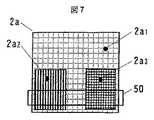
図2に検査対象となるウェハの外観を示す。ウェハ1にはダイ2毎に同様のパターンが形成されている。例えば、メモリとロジック回路を混載した半導体製品では、ダイ(チップ)の領域毎に周辺回路領域部2al,ロジック回路領域部2a2,メモリ領域部2a3等に区分けされる。それぞれの領域に形成されているパターンの幅や密度は、一般に異なる。ここでは、各領域のパターン幅とパターン密度を以下のように仮定する。(i)周辺回路領域部2alは、パターン幅が太く、パターンの密度も低い。(ii)ロジック回路領域部2a2はパターン幅は微細であるが、パターン密度が比較的低い。(iii)メモリ領域部2a3は、パターン幅が微細であり、パターン密度も高い。
【0024】
これらの領域を通常の明視野検出で取得した画像の例を図3に示す。検出画像のA−A部における検出光量分布では、パターン幅が太くて密度の低い周辺回路領域部2alにおいてパターンのモジュレーション(コントラスト)Mlが大きい。パターン幅が微細で密度の高いメモリ領域部2a3では、全般的に暗く検出され、モジュレーション(コントラスト)M3も小さい。メモリ領域部2a3において、全体的に暗く検出されるのは、対物レンズに補足される0次回折光と高次回折光の割合が低下するためである。欠陥検査は、隣接するダイ(チップ)若しくはセルの差画像を求め、しきい値以上となる位置を欠陥と判定している。このため、検出した画像においてモジュレーションが小さい領域では感度が低下する。従って、ダイ(チップ)内全域において、欠陥検出感度を均一にするためには、パターン幅やパターン密度に影響されることなく、モジュレーションを同等にすることが望ましい。
【0025】
図4に0次光検出率(透過率)を40%程度に設定した場合の検出画像を示す。メモリ領域部2a3でモジュレーションが小さくなるのは高次回折光を対物レンズ151で細くできる割合が低下するためであるため、偏光状態調整部152、153等を調整して0次回折光を減衰させることにより、0次回折光と高次回折光の振幅を同等程度に検出し、干渉によるモジュレーションM31を向上させることができる。また、パターン幅の太い周辺回路領域部2alにおいても0次回折光が減衰するため、0次光減衰前に比べて明レベルが低下する。従って、偏光状態調整部152、153等を調整して0次回折光を減衰させると検出される光量が低下するため、照明光量を多くする必要があるが、パターン幅の微細な領域のモジュレーションを向上することが可能となる。このため、微細パターン部での検査感度を向上できる。
【0026】
また、検査対象がメモリ搭載ウェハである場合は、メモリ部をセル比較し、それ以外の領域をダイ比較する。方式として、両者を2回に分けて検査する方式と両者を1回で行う混合検査方式がある。混合検査は短時間で検査できるたゆ、性能上有利である。さらに、本技術の0次回折光減衰によるセル部のモジュレーション拡大により、検査感度も向上することが可能となる。
【0027】
検査対象となるウェハ毎にパターン幅やパターン密度は異なるため、欠陥検査に用いる0次光検出率を何パーセントに設定するかを事前に条件出しする必要がある。図6に検査フローを示す。
【0028】
まず、検査対象となるウェハ1を検査装置内のローダー41にローデイングし(S61)、このローデイングされたウェハ1の種類に応じてウェハ内のダイ配列情報をCADシステム(図示せず)から入力手段を用いてオペレーテイングコントローラ35に入力して例えばデータサーバー31に登録する(S62)。次にダイ内の検査エリアの座標を同様にオペレーテイングコントローラ35に入力して例えばデータサーバー31に登録する(S63)。次に、ウェハ搬送ロボット40は、ウェハ1をローダー41からステージ上に搭載する。そして、ステージを移動させてウェハ1の所定のチップを、例えば、チップ全域検出光学系20の視野内に入れてカメラでそのチップ全域の画像を撮像し、画像処理部30に転送してデータサーバー31に保存され、更にデイスプレイ上に表示される。この表示された画面上で、外観検査用光学系15で0次光検出率(Ib/Ia)を条件出しするために画像を取得する領域が選択されてオペレーテイングコントローラ35に入力される(S64)。
【0029】
以降、外観検査用光学系15、画像処理部30、データサーバー31およびオペレーテイングコントローラ35等を用いて行う。
【0030】
次いで、外観検査用光学系15についての初期光学条件(例えば、偏光状態調整部152、153での初期偏光の状態や、光源15の初期照度など)を設定し(S65)、ステージを移動させてウェハ1上の上記選択された領域を外観検査用光学系15の視野に入れて、イメージセンサ154により条件出し領域の画像を撮像して取得する(S66)。次に、画像処理部30において、取得した画像のモジュレーション(コントラスト)を評価する(S67)。次に、オペレーテイングコントローラ35からの指令に基づいて、メカニカルコントローラ32を介して回転駆動源156を駆動して波長板152を微小回転させて0次回折光検出率を変更し、再度画像取得と画像評価を行う(S66、S67)。画像処理部30は、画像を評価し終えた時点で、0次光検出率毎に求めた図11に示す画像評価値をデーダサーバー31に記憶し、デイスプレイの画面に一覧表示する(S68)。
【0031】
オペレーテイングコントローラ35は、画面上において、上記評価値が高くなる0次光検出率を複数条件に絞り込む(S69)。次に、外観検査用光学系15および画像処理部30を用いて再度疑似欠陥を含む感度でテスト検査を行い(S70)、実欠陥か疑似欠陥かを分類する(S71)。この分類された実欠陥及び疑似欠陥部の画像を、再度外観検査用光学系15を用いて絞り込んだ0次光検出率毎に検出し、画像処理部30においてそれぞれの差画像を演算する(S72)。次に、画像処理部30は、各0次光検出率毎に疑似欠陥部の最大濃淡差Nmaxを求める(S73)。次に、画像処理部30は、それぞれの0次回折光検出率について、Nmaxに一定の値αを検査しきい値とした場合に、検出可能な実欠陥数を算出する(S74)。このように、それぞれの0次回折光検出率について、テスト検査によって得られる差画像に対して(Nmax+α)の検査しきい値で判定するので、擬似欠陥が排除された実欠陥数が算出されることになる。そして、オペレーテイングコントローラ35は、それぞれの0次光検出率の中で、最も多く実欠陥を検出できる0次光検出率(透過率)を上記外観検査用光学系15における実際の検査用の条件として設定する(S75)。次に、外観検査用光学系15および画像処理部30を用いて、検査しきい値を[Nmax+α]として、特定の領域をテスト検査し(S76)、予定の感度を満足していれば(S77)、条件出しは終了である(S78)。次に、外観検査用光学系15および画像処理部30を用いた本検査は、ダイ(チップ)内の各領域毎に先に条件出しした感度で行う。
【0032】
図7に0次光検出率の条件出しを行うために取得する画像領域50の模式図を示す。ダイ内でパターン幅やパターン密度を複数個にセグメントできる場合は、それぞれの領域を含むように領域50を設定することが望ましい。但し、予めセグメントするための情報がない場合は、ダイの中央フィールドをデフォルトで設定する等が考えられる。また、図5に示す低倍率のチップ全域検出光学系20で取得した画像を用いて、画像取得領域を決定することも可能である。
【0033】
図8にそれぞれの0次光検出率で取得した画像を微分し、その総和を求めた結果の例を示す。この計算結果では、0次光検出率40%程度が最も微分値の総和が高く、欠陥検査上、有利であると見られる。この徹分値の総和から、0次光検出率40%と60%の2つの条件に絞り込み、図6で示した実欠陥部と疑似欠陥部の画像を取得して本検査に用いる0次光検出率条件を決定する。
【0034】
図9に画像処理部30のブロック図を示す。ウェハ1の像を対物レンズ151でイメージセンサ154上に拡大投影する。イメージセンサ154の出力信号をAD変換部60でデジタル信号に変換する。一方のデジタル信号は画像評価部61に送られて画質を評価し、更に検出画像を出力する。他方のデジタル信号は遅延メモリ62に一旦格納されて、チップ比較若しくはセル比較の参照画像が出力される。それぞれの信号は画像位置合わせ部63で、検出画像と参照画像との位置合わせを行う。次に差画像算出部64で検出画像と差画像を算出し、差の特徴量を欠陥判定部65に送る。この欠陥判定部65で、検査しきい値以上となる特徴量の座標を求める。この位置が欠陥候補となり、欠陥候補の座標や特徴量などは、欠陥記憶部66に格納される。この欠陥記憶部66のデータは、データサーバ70に送られてハードディスク等に保存される。
【0035】
図10に0次光検出率を条件出しするための評価値(図6に示すステップS67で画像評価部61において実行される画質の評価値)の一つである2次微分値(2次元方向の微分値:ラプラシアンフィルター)の演算内容を示す。例えば、2次微分値(2次元方向の微分値)を求める画素の光量をI(x,y)とする。このI(x,y)と隣接する8画素の差をそれぞれについて求め、8つの差分値の絶対値の和をI(x,y)の2次微分値とする。これを、検出した画像の各画素について行い、各画素で求めた2次微分値の総和を画質の評価値とするものである。
【0036】
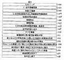
図11に0次光検出率を絞り込む評価値の一覧(図6に示すステップ68で表示する。)を示す。
微分値は各0次光検出率で検出した画像を2次微分し、微分値の総和を演算するものである。演算は図10で説明した内容である。
【0037】
次に、局所領域の最大濃淡差について説明する。検出した画像を一定の領域に区分けし、区分けした領域内で濃淡値の最小値と最大値を求め、これらの差を最大濃淡差とする。この最大濃淡差を区分けした領域全てで求め、これらの絶対値の総和を求める。領域を区分けする一例として、例えば画像のX,Y方向の画素数を3画素×3画素を1セグメントとする。この1セグメントには9画素分の明るさ情報が含まれているため、この9画素の最大値と最小値を求めて差を求めることにより、1セグメント分の濃淡差が求まる。この1セグメントの濃淡差は、セグメント内におけるパターン像のモジュレーション(コントラスト)を求めており、この最大濃淡差が大きいほど欠陥検出上有利である。従って、最大濃淡差の総和も大きい方が、欠陥検出上有利であるため、この総和値の高い0次光検出率条件を本検査用条件の候補として絞り込むことが考えられる。尚、ここで示す最大濃淡差には、画像のサンプリング誤差や局所的な照明分布のばらつきなどのウェハのパターン情報以外のばらつきを含んでいない。
【0038】
次に、濃淡分散値について説明する。画像を一定の領域に区分けし、区分けした領域内で濃淡値の分散を求める。この分散値を区分けした全ての領域で求め、これらの総和を求める。区分け領域の一例として、3×3画素を1セグメントに設定する。尚、この分散値は、局所領域内における濃淡のばらつきを示しており、この分散値が大きいほどパターン情報が高くなる。従って、分散値の大きい方が欠陥検出上有利である。尚、ここで示す濃淡のばらつきには、画像のサンプリング誤差や局所的な照明分布のばらつきなどのウェハのパターン情報以外のばらつきを含んでいない。
【0039】
次に画像フーリエ密度に関する評価手法について説明する。画像のX,Y方向に2次元フーリエ変換を行い、特定の周波数以上のスペクトル密度の総和を評価値とする。特定の周波数とは、パターンピッチやイメージセンサの1画素あたりの寸法をウェハ上の寸法に換算した値などを基準に決定する。この特定の周波数以上のスペクトル密度が高いといことは、特定の周波数に対応するパターンピッチ寸法以下の微細パターンにおいて、画像のモジュレーションが高いことを意味している。従って、特定の周波数以上のスペクトル密度が高い方が、欠陥検出上有利である。また、特定の周波数のみのスペクトル密度を評価値として用いる事が考えられる。
【0040】
上記した実施例においては、モジュレーション(コントラスト)を調整する手段として、0次光検出率(透過率)(Ib/Ia)を調整する偏光状態調整部152、153を用いた場合について説明したが、空間フィルタを用いても0次光検出率(透過率)(Ib/Ia)を調整することが可能で、同様の効果を得ることが出来る。この場合、0次光の透過率を変更するには、空間フィルタをそれぞれの検出率に対応したものに切り替えるか、又は、空間フィルタのパターンを可変の構造としておいてそれぞれの検出率に対応したパターンを形成するようにすれば良い。
【0041】
以上、複数種類の評価値について説明したが、実際に用いる評価値は単独あるいは2種類以上の評価値を用いて0次光低減率の絞り込みに用いても構わない。
【0042】
また、0次光低減率以外にも以下の光学パラメータがある。
【0043】
(i)照明c(照明の入射角範囲の設定)
(ii)照明波長域
(iii)対物レンズの開口数
これらの条件を絞り込む場合にも本評価値を有効に活用できる。これにより、短時間に検査感度上有利な光学条件に設定することが可能となる。
【0044】
さらに、本発明の特徴とする構成について説明する。
【0045】
即ち、本発明は、落射照明による試料の光学像を0次回折光の透過率を変更して撮像して画像を検出し、該検出した試料の画像の画質を評価して、欠陥検出感度が高くなる0次回折光検出率を求め、この0次回折光検出率となる光学条件に設定するステップと、該設定された光学条件で落射照明による試料の光学像を撮像して画像を検出し、該検出した試料の画像に基づいて欠陥を検出して検査する実検査ステップとを有することを特徴とする。
【0046】
上記画質評価手法として、前記試料の各領域において検出した画像の明るさの差を求め、この差が小さくなる0次光検出率が最適であると判定することを特徴とする。
【0047】
また、上記画質評価手法として、前記試料の各領域において検出した画像を2次微分し、画像内の2次微分値の総和を求め、この総和が大きくなる0次光検出率が最適であると判定することを特徴とする。
【0048】
また、上記画質評価値の高い複数の0次回折光検出率条件を選択し、予め実欠陥と疑似欠陥を分類した欠陥の画像をそれぞれの0次光検出率条件で取得し、欠陥部の濃淡差が大きく、疑似欠陥部の濃淡差が小さい0次光検出率条件を選択して検査することを特徴とする。
【0049】
また、本発明は、試料1を搭載するステージと、前記試料で正反射した光の検出率を制御する光学素子152、153と、該光学素子153を透過した光をイメージセンサ154上に結像させる結像光学系(図示せず)と、前記イメージセンサの出力信号をデジタル画像に変換する変換器60と、前記デジタル画像を用いて前記試料の画質を評価する画質処理部30と、前記評価値の高い正反射光の検出率に設定する設定部35、32、156、157を具備したことを特徴とする欠陥検査装置である。
【0050】
また、上記画質処理部30として、検出した画像の複数位置における明るさ或いはパターンのモジュレーションを求める評価値処理部と、評価値から検査感度が高い条件を選択する判定部と、判定した光学条件で前記試料を検査する機能を具備したことを特徴とする。
【0051】
また、本発明は、試料1を偏光照明する照明光学系155,153,152と、光学素子153を透過した光をイメージセンサ154上に結像させる結像光学系と、該結像光学系に特定の偏光をフィルタリングするフィルタリング部153と、前記イメージセンサの出力信号をデジタル画像に変換する変換部60と、該変換部で変換したデジタル画像を用いて前記試料の画質を評価する画質処理部30と、該画質処理部で前記試料の画質を評価して評価値の高いデジタル画像の正反射光の透過率に設定する設定部35、32、156、157を具備したことを特徴とする。
【0052】
上記画質処理部として、前記試料の各領域において検出した画像の明るさの差を演算する演算部と、この差が小さくなる0次光検出率が最適であると判定する判定部を具備したことを特徴とする。
【0053】
また、上記画質処理部として、前記試料め各領域において検出した画像を2次徹分する微分処理部と、画像内の2次微分値の総和を求める加算処理部と、この加算値が大きくなる0次光検出率が最適であると判定する判定部を具備したことをを特徴とする。
【0054】
また、上記設定部として、上記画質処理部の出力が高い複数の0次光検出率条件を選択する選択部と、予め実欠陥と疑似欠陥を分類した欠陥の画像をそれぞれの0次光検出率条件で取得する画像検出部と、欠陥部及び疑似欠陥部の濃淡差を求める差画像検出部と、疑似欠陥を検出しない検査官度で最も多く実欠陥を検出できる0次光検出率条件を選択する選択部と、前記選択部で選ばれた条件で検査する機能を具備したことを特徴とする。
【0055】
【発明の効果】
以上に説明したごとく、本発明によれば、微細パターン部のモジュレーション(コントラスト)を向上することにより、微細パターン部における欠陥検出感度を向上することが可能となる。微細パターン部のモジュレーション向上用光学条件出しについても各パラメータを短時間で設定することが可能となり、検査レシピ作成時間も大幅に省略できる。
【図面の簡単な説明】
【図1】図1は、0次光透過率(0次光検出率)と画像コントラストの関係を示すグラフである。
【図2】図2は、メモリ混載ロジック製品用ウェハの外観を示す平面図である。
【図3】図3は、従来の明視野照明による検出画像の例を示す平面図および光量分布図である。
【図4】図4は、0次光検出率を低減した場合の検出画像の例を示す平面図および光量分布図である。
【図5】図5は、本発明に係る検査装置の概略構成を示す正面図である。
【図6】図6は、0次光検出率の条件出しの手順を示すフローチャートである。
【図7】図7は、条件出し用画像取得領域の一例を示す画像の平面図である。
【図8】図8は、画像評価結果の一例を示す図である。
【図9】図9は、本発明に係る画像処理部の概略構成を示すブロック図である。
【図10】図10は、2次微分の演算内容を示す図である。
【図11】図11は、画質評価項目とその内容の関係の一例を示す図である。
【符号の説明】
1…ウェハ(試料)、2、2a…ダイ(チップ)、2a1…周辺回路領域部、2a2…ロジック回路領域部、2a3…メモリ領域部、10…θステージ、11…Zステージ、12…Xステージ、13…Yステージ、15…外観検査用光学系、20…チップ全域検出光学系、21…カメラ、30…画像処理部、31…データサーバー、32…メカコントローラー、35…オペレーティングコントローラー、45…欠陥検査装置、60…AD変換部、61…画像評価部61、62…遅延メモリ、63…画像位置合わせ部、64…差画像算出部、65…欠陥判定部、66…欠陥記憶部、70…データサーバ、151、202…対物レンズ、152…1/2、1/4波長板(偏光状態調整部)、153…偏光ビームスプリッタ、154…イメージセンサ、155…光源、156…回転駆動源、157…回転伝達手段。[0001]
BACKGROUND OF THE INVENTION
The present invention relates to a high-resolution optical system used for inspection and observation of fine pattern defects and foreign matters typified by semiconductor manufacturing processes and flat panel display manufacturing processes, and a defect inspection method and apparatus using the same.
[0002]
[Prior art]
As a conventional technique, Japanese Patent Laid-Open No. 8-327554 discloses a technique for improving the contrast of an object by changing the incident angle of illumination according to the optical characteristics of the object to be observed.
[0003]
[Problems to be solved by the invention]
In the conventional technique described above, in order to make the fine unevenness on the surface of the object special, the incident angle of illumination is determined so as to increase the contrast of the unevenness by changing the incident angle of the illumination. In such a system, an oblique illumination / diagonal detection system is employed as an optical system, and by changing the incident angle of the oblique illumination, the object is continuously observed from bright field illumination to dark field illumination. The appearance is changed. However, in the case of dark field brightening, for example, when there is a defect such as a thin film remaining on the object, detection becomes difficult. Further, when the inspection target is a semiconductor device, minute irregularities (grains) are generated on the surface of the metal wiring formed in the metal wiring process. However, since this grain is not fatal as a semiconductor device, it should not be detected as a defect. However, in the conventional technology, this grain is reliably identified from other defects to detect defects with high reliability. It was difficult.
[0004]
An object of the present invention is to realize defect detection with high reliability, which has been difficult to achieve with the above-described prior art.
[0005]
[Means for Solving the Problems]
In order to achieve the above object, the present invention uses a coaxial incident bright field illumination optical system to change the transmittance of zero-order diffracted light that is specularly reflected from a sample to form an optical image of the sample and capture it with an image sensor. By doing so, a sample image with high resolution is obtained.
[0006]
In the present invention, an image signal of the sample is obtained by imaging the sample through the optical system, and a plurality of positions of the sample in the image signal (for example, the peripheral circuit region portion, the logic circuit region portion, the memory region portion, etc.) The optical conditions of the optical system were adjusted so that the difference in brightness (contrast) or pattern modulation (contrast) at locations (local areas or segments) corresponding to multiple circuit areas was reduced. An image signal of the sample whose optical conditions are adjusted is obtained by imaging the sample through the optical system in a state, and the image signal is processed to detect a defect (pattern defect, defect such as foreign matter) of the sample. .
[0007]
In addition, the present invention obtains an image signal of a sample by imaging the sample by epi-illuminating the sample, and a plurality of positions of the sample in the image signal (for example, a peripheral circuit region portion, a logic circuit region portion, and a memory region portion) The next time of the reflected light from the sample due to illumination so that the difference in brightness (contrast) or pattern modulation (contrast) at a location (local region or segment) corresponding to a plurality of circuit regions such as The sample in which the detection rate (transmittance) of the folded light (regular reflection light) is adjusted, and the detection rate of the 0th-order diffracted light is adjusted by imaging the sample in a state where the detection rate (transmittance) of the 0th-order diffracted light is adjusted The image signal is obtained, and the image signal is processed to detect a defect of the sample (pattern defect, defect such as foreign matter).
[0008]
Further, in the present invention, a plurality of images having different transmittances of the 0th-order diffracted light are obtained by epi-illuminating the sample and imaging the sample by changing the transmittance of the 0th-order diffracted light among the reflected light from the sample by illumination, Using this plurality of images, a transmittance condition for the 0th-order diffracted light that increases the defect detection sensitivity is obtained, and the transmittance condition for obtaining the transmittance of the 0th-order diffracted light among the reflected light from the sample is set. The sample is imaged in the state set to the rate condition to obtain an image, and the defect of the sample is detected using the image obtained in the state set to the transmittance condition.
[0009]
Furthermore, in the present invention, the sample is incident-light illuminated with polarized light, the illuminated sample is imaged to obtain an image of the sample, and the polarization state of the reflected light from the sample by illumination based on the contrast information of the sample image The sample with the adjusted polarization state of the reflected light is imaged to obtain an image of the sample, and the defect of the sample is detected using this image.
[0010]
In the present invention, the plurality of circuit areas divided in the chips arranged on the wafer are incidentally illuminated, and the reflected light images from each of the plurality of circuit areas have a mutual transmittance of the 0th-order diffracted light. The defect inspection method is characterized in that an image signal is obtained by changing the image to obtain an image signal, and the obtained image signal is processed to detect a defect.
[0011]
As described above, according to the present invention, for example, a high-resolution image can be obtained in a memory area portion having a fine pattern width and a high pattern density. In addition, it is possible to automatically set high contrast optical conditions in a short time.
[0012]
DETAILED DESCRIPTION OF THE INVENTION
An embodiment of the present invention is shown in FIG. 45 is a defect inspection apparatus according to the present invention.
A sample (wafer) 1 is stored in a
[0013]
Next, the actual inspection is performed by the high magnification visual inspection
[0014]
The mechanical operation units such as the stage and the
[0015]
Next, a high-magnification appearance inspection
[0016]
High-order diffracted light (second-order or higher-order diffracted light) generated from the edge of the pattern in the region is condensed by the
[0017]
Ib indicates the intensity of the 0th-order diffracted light transmitted through the
[0018]
Ia indicates the intensity of the 0th-order diffracted light input to the
[0019]
In another embodiment, in the
[0020]
As described above, the minute rotation adjustment of the
[0021]
The
[0022]
FIG. 1 shows the relationship between the 0th-order light detection rate (Ib / Ia) and the pattern contrast of the detected image. A zero-order light detection rate of 100% is the same image as that detected by the normal bright field detection method. When the polarization state is adjusted by the polarization
[0023]
FIG. 2 shows the appearance of a wafer to be inspected. A similar pattern is formed on the
[0024]
FIG. 3 shows an example of an image obtained by obtaining these areas by normal bright field detection. In the detected light amount distribution in the AA portion of the detected image, the pattern modulation (contrast) Ml is large in the peripheral circuit region portion 2al having a thick pattern width and a low density. The memory area 2a3 having a fine pattern width and high density is generally detected dark, and the modulation (contrast) M3 is also small. The reason why the entire area is detected dark in the memory area 2a3 is that the ratio of the 0th-order diffracted light and the high-order diffracted light captured by the objective lens decreases. In the defect inspection, a difference image between adjacent dies (chips) or cells is obtained, and a position that is equal to or higher than a threshold value is determined as a defect. For this reason, the sensitivity decreases in a region where the modulation is small in the detected image. Therefore, in order to make the defect detection sensitivity uniform over the entire area within the die (chip), it is desirable to make the modulations equal without being affected by the pattern width or pattern density.
[0025]
FIG. 4 shows a detected image when the zero-order light detection rate (transmittance) is set to about 40%. The modulation is reduced in the memory area 2a3 because the rate at which the high-order diffracted light can be thinned by the
[0026]
When the inspection target is a memory-mounted wafer, the memory portion is subjected to cell comparison, and the other regions are subjected to die comparison. As a method, there are a method in which both are inspected in two times and a mixed inspection method in which both are in one time. The mixed inspection is advantageous in terms of performance because it can be inspected in a short time. Furthermore, inspection sensitivity can also be improved by expanding the modulation of the cell portion by attenuation of the 0th-order diffracted light of the present technology.
[0027]
Since the pattern width and pattern density differ for each wafer to be inspected, it is necessary to determine in advance what percentage the 0th-order light detection rate used for defect inspection is set. FIG. 6 shows an inspection flow.
[0028]
First, a
[0029]
Thereafter, the visual inspection
[0030]
Next, initial optical conditions for the appearance inspection optical system 15 (for example, the initial polarization state in the polarization
[0031]
On the screen, the operating controller 35 narrows down the 0th-order light detection rate at which the evaluation value is high to a plurality of conditions (S69). Next, the test inspection is performed again with the sensitivity including the pseudo defect using the
[0032]
FIG. 7 shows a schematic diagram of an
[0033]
FIG. 8 shows an example of the result obtained by differentiating the images acquired at the respective 0th-order light detection rates and obtaining the sum. In this calculation result, a zero-order light detection rate of about 40% has the highest sum of differential values, and is considered advantageous for defect inspection. Based on the sum of the total values, the two conditions of the 0th order light detection rate of 40% and 60% are narrowed down, and the images of the real defect portion and the pseudo defect portion shown in FIG. Determine the detection rate conditions.
[0034]
FIG. 9 shows a block diagram of the
[0035]
FIG. 10 shows a secondary differential value (two-dimensional direction) which is one of evaluation values for determining the 0th-order light detection rate (image quality evaluation value executed in the
[0036]
FIG. 11 shows a list of evaluation values for narrowing down the 0th-order light detection rate (displayed in step 68 shown in FIG. 6).
The differential value is obtained by secondarily differentiating the image detected at each 0th-order light detection rate and calculating the sum of the differential values. The calculation is as described in FIG.
[0037]
Next, the maximum gray level difference in the local area will be described. The detected image is divided into certain areas, and the minimum and maximum gray values are determined in the divided area, and the difference between them is defined as the maximum gray difference. It calculates | requires in all the area | regions which divided this maximum contrast, and calculates | requires the total of these absolute values. As an example of dividing the region, for example, the number of pixels in the X and Y directions of the image is 3 pixels × 3 pixels as one segment. Since the brightness information for nine pixels is included in one segment, the density difference for one segment can be obtained by obtaining the maximum value and the minimum value of the nine pixels to obtain the difference. The density difference of one segment determines the modulation (contrast) of the pattern image in the segment, and the larger the maximum density difference, the more advantageous for defect detection. Therefore, since it is more advantageous for defect detection to have a larger total sum of the maximum light and shade differences, it is conceivable to narrow down the 0th-order light detection rate condition having a high total value as a candidate for this inspection condition. Note that the maximum shading difference shown here does not include variations other than wafer pattern information, such as image sampling errors and local illumination distribution variations.
[0038]
Next, the light and shade dispersion value will be described. The image is divided into certain areas, and the variance of the gray value is obtained in the divided area. This variance value is obtained in all divided areas, and the sum of these is obtained. As an example of the segmented area, 3 × 3 pixels are set as one segment. This variance value indicates the variation in shading within the local region, and the pattern information becomes higher as the variance value is larger. Therefore, a larger dispersion value is advantageous for defect detection. The shading variation shown here does not include variations other than wafer pattern information such as image sampling error and local illumination distribution variation.
[0039]
Next, an evaluation method related to the image Fourier density will be described. Two-dimensional Fourier transform is performed in the X and Y directions of the image, and the sum of spectral densities over a specific frequency is used as an evaluation value. The specific frequency is determined based on a pattern pitch or a value obtained by converting a size per pixel of the image sensor into a size on the wafer. The fact that the spectral density equal to or higher than the specific frequency is high means that the modulation of the image is high in a fine pattern having a pattern pitch dimension or less corresponding to the specific frequency. Therefore, a higher spectral density above a specific frequency is advantageous for defect detection. It is also conceivable to use the spectral density of only a specific frequency as the evaluation value.
[0040]
In the above-described embodiments, the case where the polarization
[0041]
Although a plurality of types of evaluation values have been described above, the evaluation values that are actually used may be used for narrowing down the zero-order light reduction rate by using single or two or more types of evaluation values.
[0042]
In addition to the 0th-order light reduction rate, there are the following optical parameters.
[0043]
(I) Illumination c (setting of incident angle range of illumination)
(Ii) Illumination wavelength range
(Iii) Numerical aperture of the objective lens
This evaluation value can be used effectively when narrowing down these conditions. This makes it possible to set optical conditions that are advantageous in terms of inspection sensitivity in a short time.
[0044]
Further, a configuration that characterizes the present invention will be described.
[0045]
That is, according to the present invention, an optical image of a sample by epi-illumination is picked up by changing the transmittance of the 0th-order diffracted light to detect the image, and the image quality of the detected sample image is evaluated, and the defect detection sensitivity is high. A zero-order diffracted light detection rate is obtained and set to an optical condition that achieves this zero-order diffracted light detection rate; and an optical image of the sample by epi-illumination is captured under the set optical condition to detect the image, and the detection And an actual inspection step of detecting and inspecting the defect based on the sample image.
[0046]
As the image quality evaluation method, a difference in brightness of images detected in each region of the sample is obtained, and it is determined that a zero-order light detection rate at which the difference is small is optimal.
[0047]
Further, as the image quality evaluation method, the image detected in each region of the sample is second-order differentiated to obtain the sum of the second-order derivative values in the image, and the zero-order light detection rate at which this sum is large is optimal. It is characterized by determining.
[0048]
In addition, a plurality of 0th-order diffracted light detection rate conditions with high image quality evaluation values are selected, and images of defects in which real defects and pseudo defects are classified in advance are acquired under the respective 0th-order light detection rate conditions. Is characterized by selecting and inspecting a zero-order light detection rate condition that is large and has a small shade difference in the pseudo defect portion.
[0049]
Further, the present invention forms an image on the
[0050]
The image
[0051]
The present invention also provides illumination
[0052]
The image quality processing unit includes a calculation unit that calculates a difference in brightness of images detected in each region of the sample, and a determination unit that determines that the 0th-order light detection rate at which the difference is small is optimal. It is characterized by.
[0053]
In addition, as the image quality processing unit, a differential processing unit for secondarily dividing the image detected in each region of the sample, an addition processing unit for obtaining a sum of secondary differential values in the image, and the addition value is increased. A determination unit that determines that the 0th-order light detection rate is optimum is provided.
[0054]
In addition, as the setting unit, a selection unit that selects a plurality of 0th-order light detection rate conditions for which the output of the image quality processing unit is high, and a defect image in which real defects and pseudo-defects are classified in advance are displayed as respective 0th order light detection rates. Select the image detection unit that is acquired under the conditions, the difference image detection unit that obtains the density difference between the defective part and the pseudo defect part, and the 0th-order light detection rate condition that can detect the most real defects with the degree of inspector that does not detect the pseudo defect And a function of inspecting under a condition selected by the selection unit.
[0055]
【The invention's effect】
As described above, according to the present invention, it is possible to improve the defect detection sensitivity in the fine pattern portion by improving the modulation (contrast) of the fine pattern portion. Each parameter can be set in a short time for the optical condition for improving the modulation of the fine pattern portion, and the inspection recipe preparation time can be largely omitted.
[Brief description of the drawings]
FIG. 1 is a graph showing the relationship between 0th-order light transmittance (0th-order light detection rate) and image contrast.
FIG. 2 is a plan view showing an appearance of a wafer for memory-embedded logic products.
FIGS. 3A and 3B are a plan view and a light amount distribution diagram showing an example of a detection image by conventional bright field illumination. FIGS.
FIGS. 4A and 4B are a plan view and a light amount distribution diagram showing an example of a detected image when the 0th-order light detection rate is reduced. FIGS.
FIG. 5 is a front view showing a schematic configuration of an inspection apparatus according to the present invention.
FIG. 6 is a flowchart illustrating a procedure for setting a condition for a 0th-order light detection rate.
FIG. 7 is a plan view of an image showing an example of an image acquisition area for condition determination.
FIG. 8 is a diagram illustrating an example of an image evaluation result.
FIG. 9 is a block diagram illustrating a schematic configuration of an image processing unit according to the present invention.
FIG. 10 is a diagram illustrating calculation contents of second-order differentiation.
FIG. 11 is a diagram illustrating an example of a relationship between image quality evaluation items and their contents.
[Explanation of symbols]
DESCRIPTION OF
Claims (12)
Translated fromJapanese前記検査光学系により該検査用光学条件設定ステップで設定した検査用光学条件で前記検査光学系を用いてウェハ上の画像を撮像し、該撮像された検査画像信号とチップ比較若しくはセル比較用の参照画像信号とを比較してそれらの差画像信号に基づいて前記ウェハ上に存在する欠陥を検出する欠陥検査ステップと
を有する欠陥検査方法であって、
前記検査用光学条件設定ステップにおいて、
ウェハ上の条件出し領域について前記検査用光学系を用いて複数の光学条件でテスト検査を行い、該テスト検査の結果前記光学条件毎に検出される欠陥を実欠陥と擬似欠陥とに分類し、該光学条件毎に分類された実欠陥及び擬似欠陥の画像を検出してチップ比較若しくはセル比較による実欠陥及び擬似欠陥の差画像を算出し、該光学条件毎に算出された擬似欠陥の差画像を基に擬似欠陥部の最大濃淡差を求め、該光学条件毎に算出された実欠陥の差画像に対して前記求められた擬似欠陥部の最大濃淡差に応じた検査しきい値で判定して擬似欠陥が排除された実欠陥の数を算出し、該光学条件毎に算出された実欠陥の数が前記複数の光学条件の内最も多く検出できる光学条件を選んで前記検査用光学条件として設定することを特徴とする欠陥検査方法。Inspection optical condition setting step for setting inspection optical conditions for imaging using an inspection optical system having an illumination optical system and a detection optical system at the time of inspection;
The inspection optical system captures an image on the wafer using the inspection optical system under the inspection optical conditions set in the inspection optical condition setting step, and the captured inspection image signal is used for chip comparison or cell comparison. A defect inspection step of comparing a reference image signal and detecting a defect present on the wafer based on the difference image signal;
A defect inspection method comprising:
In the inspection optical condition setting step,
Perform test inspection under a plurality of optical conditions using the inspection optical system for the condition setting area on the wafer, classify the defects detected for each optical condition as a result of the test inspection into real defects and pseudo defects, Real defect and pseudo defect images classified for each optical condition are detected to calculate a difference image between the real defect and the pseudo defect by chip comparison or cell comparison, and the pseudo defect difference image calculated for each optical condition Based on the above, the maximum gray level difference of the pseudo defect portion is obtained, and the difference image of the actual defect calculated for each optical condition is determined by the inspection threshold value according to the obtained maximum gray level difference of the pseudo defect portion. Calculating the number of actual defects from which the pseudo defects have been eliminated, and selecting the optical condition that can detect the largest number of the actual defects calculated for each optical condition as the optical condition for inspection. defect detection, characterized inthat theset Method.
前記検査用光学条件条件設定ステップで設定した検査用光学条件で前記検査用光学系を用いてウェハ上の画像を撮像し、該撮像された検査画像信号とチップ比較若しくはセル比較用の参照画像信号とを比較してそれらの差画像信号に基づいて前記ウェハ上に存在する欠陥を検出する欠陥検査ステップとを有することを特徴とする欠陥検査方法。A test inspection is performed under a plurality of optical conditions using an inspection optical system having an illumination optical system and a detection optical system for the condition-determining area on the wafer, and the defects detected for each optical condition as a result of the test inspection are actual defects. And the actual defect and pseudo-defect image classified for each optical condition are detected and a difference image between the actual defect and the pseudo-defect is calculated by chip comparison or cell comparison, for each optical condition. Based on the calculated difference image of the pseudo defect, the maximum density difference of the pseudo defect portion is obtained, and the difference image of the actual defect calculated for each optical condition is determined according to the obtained maximum density difference of the pseudo defect portion. The number of actual defects from which pseudo defects have been eliminated by calculating with the inspection threshold is calculated, and the number of actual defects calculated for each optical condition is the optical condition that can be detected most among the plurality of optical conditions. Select the inspection light during inspection And the examination optical condition setting step of setting as the examination optical conditions for imaging using the system,
An image on the wafer is captured using the inspection optical system under the inspection optical conditions set in the inspection optical condition setting step, and the captured inspection image signal and a reference image signal for chip comparison or cell comparison And a defect inspection step of detecting a defect existing on the wafer based on the difference image signal .
該検査用光学系の検出光学系で撮像して得た検査画像信号とチップ比較若しくはセル比較用の参照画像信号とを比較してそれらの差画像信号に基づいてウェハ上に存在する欠陥を検出する画像処理部とを備えた欠陥検査装置であって、
検査時における前記検査用光学系の検査用光学条件を設定する検査用光学条件設定手段を備え、該検査用光学条件設定手段は、ウェハ上の条件出し領域について前記検査用光学系を用いて複数の光学条件でテスト検査を行い、該テスト検査の結果前記光学条件毎に検出される欠陥を実欠陥と擬似欠陥とに分類し、該光学条件毎に分類された実欠陥及び擬似欠陥の画像を検出してチップ比較若しくはセル比較による実欠陥及び擬似欠陥の差画像を算出し、該光学条件毎に算出された擬似欠陥の差画像を基に擬似欠陥部の最大濃淡差を求め、該光学条件毎に算出された実欠陥の差画像に対して前記求められた擬似欠陥部の最大濃淡差に応じた検査しきい値で判定して擬似欠陥が排除された実欠陥の数を算出し、該光学条件毎に算出された実欠陥の数が前記複数の光学条件の内最も多く検出できる光学条件を選んで前記検査用光学条件として設定するように構成し、
検査時において、前記検査用光学条件設定手段で設定された検査用光学条件になるように前記検査用光学系を調整することを特徴とする欠陥検査装置。An inspection optical system having an illumination optical system that illuminates the wafer and a detection optical system that captures an image on the wafer illuminated by the illumination optical system;
The inspection image signal obtained by imaging with the detection optical system of the inspection optical system is compared with a reference image signal for chip comparison or cell comparison, and a defect present on the wafer is detected based on the difference image signal. A defect inspection apparatus comprising an image processing unit for performing
An inspection optical condition setting means for setting an inspection optical condition of the inspection optical system at the time of inspection is provided, and the inspection optical condition setting means includes a plurality of condition setting areas on the wafer using the inspection optical system. The test inspection is performed under the optical conditions, and the defects detected for each optical condition as a result of the test inspection are classified into real defects and pseudo defects, and images of real defects and pseudo defects classified according to the optical conditions are obtained. Detecting and calculating a difference image between a real defect and a pseudo defect by chip comparison or cell comparison, obtaining a maximum gray level difference of the pseudo defect portion based on the difference image of the pseudo defect calculated for each optical condition, and the optical condition The actual defect difference image calculated every time is determined by the inspection threshold value according to the obtained maximum gray level difference of the pseudo defect portion, and the number of real defects from which the pseudo defect is eliminated is calculated, Actual defects calculated for each optical condition There was configured to set a most optical conditions for the test to select the optical conditions that can be detected among the plurality of optical conditions,
A defect inspection apparatus, wherein the inspection optical system is adjusted so that the inspection optical condition set by the inspection optical condition setting means is satisfied at the time of inspection .
Priority Applications (1)
| Application Number | Priority Date | Filing Date | Title |
|---|---|---|---|
| JP2001386253AJP3784711B2 (en) | 2000-12-20 | 2001-12-19 | Defect inspection method and apparatus |
Applications Claiming Priority (3)
| Application Number | Priority Date | Filing Date | Title |
|---|---|---|---|
| JP2000391825 | 2000-12-20 | ||
| JP2000-391825 | 2000-12-20 | ||
| JP2001386253AJP3784711B2 (en) | 2000-12-20 | 2001-12-19 | Defect inspection method and apparatus |
Publications (2)
| Publication Number | Publication Date |
|---|---|
| JP2002277404A JP2002277404A (en) | 2002-09-25 |
| JP3784711B2true JP3784711B2 (en) | 2006-06-14 |
Family
ID=26606460
Family Applications (1)
| Application Number | Title | Priority Date | Filing Date |
|---|---|---|---|
| JP2001386253AExpired - Fee RelatedJP3784711B2 (en) | 2000-12-20 | 2001-12-19 | Defect inspection method and apparatus |
Country Status (1)
| Country | Link |
|---|---|
| JP (1) | JP3784711B2 (en) |
Cited By (1)
| Publication number | Priority date | Publication date | Assignee | Title |
|---|---|---|---|---|
| KR102184780B1 (en)* | 2019-12-24 | 2020-11-30 | 한화에어로스페이스 주식회사 | Method and system for inspecting growth quality of graphine |
Families Citing this family (13)
| Publication number | Priority date | Publication date | Assignee | Title |
|---|---|---|---|---|
| US7006224B2 (en)* | 2002-12-30 | 2006-02-28 | Applied Materials, Israel, Ltd. | Method and system for optical inspection of an object |
| JP4706197B2 (en)* | 2003-07-15 | 2011-06-22 | オムロン株式会社 | Object determining apparatus and imaging apparatus |
| KR100839772B1 (en) | 2003-07-15 | 2008-06-20 | 오므론 가부시키가이샤 | Target determination device and imaging device |
| JP2006029881A (en) | 2004-07-14 | 2006-02-02 | Hitachi High-Technologies Corp | Pattern defect inspection method and apparatus |
| JP2007071678A (en) | 2005-09-07 | 2007-03-22 | Hitachi High-Technologies Corp | Inspection system |
| JP4914604B2 (en)* | 2005-12-07 | 2012-04-11 | 株式会社日立ハイテクノロジーズ | Pattern defect inspection method and system using electron beam inspection apparatus, and mapping projection type or multi-beam type electron beam inspection apparatus |
| CN101796398B (en)* | 2007-08-31 | 2013-06-19 | Icos视觉系统股份有限公司 | Apparatus and method for detecting semiconductor substrate anomalies |
| JP2012078164A (en)* | 2010-09-30 | 2012-04-19 | Nuflare Technology Inc | Pattern inspection device |
| KR102729956B1 (en) | 2018-08-28 | 2024-11-13 | 케이엘에이 코포레이션 | Off-axis illumination overlay measurements using imaging of 2-diffracted orders |
| CN114136975A (en)* | 2021-11-04 | 2022-03-04 | 上海精密计量测试研究所 | A kind of microwave bare chip surface defect intelligent detection system and method |
| CN117204811B (en)* | 2023-09-26 | 2025-06-06 | 深圳盛达同泽科技有限公司 | Refractive topography measurement system |
| CN118657346B (en)* | 2024-08-16 | 2024-11-12 | 深圳市宝田精工科技有限公司 | Method and system for optimizing the manufacturing process of communication module housing |
| CN118961730B (en)* | 2024-10-16 | 2025-01-07 | 深圳市领耀东方科技股份有限公司 | Intelligent and rapid detection system and method for appearance of LED chip |
- 2001
- 2001-12-19JPJP2001386253Apatent/JP3784711B2/ennot_activeExpired - Fee Related
Cited By (1)
| Publication number | Priority date | Publication date | Assignee | Title |
|---|---|---|---|---|
| KR102184780B1 (en)* | 2019-12-24 | 2020-11-30 | 한화에어로스페이스 주식회사 | Method and system for inspecting growth quality of graphine |
Also Published As
| Publication number | Publication date |
|---|---|
| JP2002277404A (en) | 2002-09-25 |
Similar Documents
| Publication | Publication Date | Title |
|---|---|---|
| US7440092B2 (en) | Method and apparatus for detecting defects | |
| JP3808169B2 (en) | Inspection method and apparatus, and semiconductor substrate manufacturing method | |
| US6928185B2 (en) | Defect inspection method and defect inspection apparatus | |
| US7333650B2 (en) | Defect inspection apparatus | |
| US7379173B2 (en) | High throughput brightfield/darkfield wafer inspection system using advanced optical techniques | |
| US7554655B2 (en) | High throughput brightfield/darkfield water inspection system using advanced optical techniques | |
| JP3784711B2 (en) | Defect inspection method and apparatus | |
| JP4009409B2 (en) | Pattern defect inspection method and apparatus | |
| JP4357355B2 (en) | Pattern inspection method and apparatus | |
| US5640237A (en) | Method and apparatus for detecting non-uniformities in reflective surafaces | |
| JP2006220644A (en) | Pattern inspection method and apparatus | |
| KR20080073281A (en) | Image defect inspection device, image defect inspection system and image defect inspection method | |
| JP2001013085A (en) | Flow inspection apparatus | |
| JP2004354250A (en) | Defect inspection device | |
| JP2010151824A (en) | Method and apparatus for inspecting pattern | |
| JP2947513B1 (en) | Pattern inspection equipment | |
| JP3376082B2 (en) | Pattern defect inspection equipment | |
| JP2001194322A (en) | Appearance inspection device and inspection method | |
| JP3657076B2 (en) | Wafer macro inspection method and automatic wafer macro inspection apparatus | |
| JP2024537955A (en) | Suppression of laser annealing patterns | |
| JP4162319B2 (en) | Defect inspection equipment | |
| JP5011348B2 (en) | Pattern inspection method and apparatus | |
| JP2002303588A (en) | Pattern defect inspection device | |
| JP2025090537A (en) | Image processing device, optical device, image processing method, and method of using optical device | |
| JP2001174417A (en) | Apparatus and method for detecting defect |
Legal Events
| Date | Code | Title | Description |
|---|---|---|---|
| A977 | Report on retrieval | Free format text:JAPANESE INTERMEDIATE CODE: A971007 Effective date:20050831 | |
| A131 | Notification of reasons for refusal | Free format text:JAPANESE INTERMEDIATE CODE: A131 Effective date:20050927 | |
| A521 | Written amendment | Free format text:JAPANESE INTERMEDIATE CODE: A523 Effective date:20051128 | |
| RD02 | Notification of acceptance of power of attorney | Free format text:JAPANESE INTERMEDIATE CODE: A7422 Effective date:20051128 | |
| TRDD | Decision of grant or rejection written | ||
| A01 | Written decision to grant a patent or to grant a registration (utility model) | Free format text:JAPANESE INTERMEDIATE CODE: A01 Effective date:20060307 | |
| A61 | First payment of annual fees (during grant procedure) | Free format text:JAPANESE INTERMEDIATE CODE: A61 Effective date:20060315 | |
| R150 | Certificate of patent or registration of utility model | Ref document number:3784711 Country of ref document:JP Free format text:JAPANESE INTERMEDIATE CODE: R150 Free format text:JAPANESE INTERMEDIATE CODE: R150 | |
| FPAY | Renewal fee payment (event date is renewal date of database) | Free format text:PAYMENT UNTIL: 20090324 Year of fee payment:3 | |
| FPAY | Renewal fee payment (event date is renewal date of database) | Free format text:PAYMENT UNTIL: 20100324 Year of fee payment:4 | |
| FPAY | Renewal fee payment (event date is renewal date of database) | Free format text:PAYMENT UNTIL: 20110324 Year of fee payment:5 | |
| FPAY | Renewal fee payment (event date is renewal date of database) | Free format text:PAYMENT UNTIL: 20110324 Year of fee payment:5 | |
| FPAY | Renewal fee payment (event date is renewal date of database) | Free format text:PAYMENT UNTIL: 20120324 Year of fee payment:6 | |
| FPAY | Renewal fee payment (event date is renewal date of database) | Free format text:PAYMENT UNTIL: 20130324 Year of fee payment:7 | |
| FPAY | Renewal fee payment (event date is renewal date of database) | Free format text:PAYMENT UNTIL: 20130324 Year of fee payment:7 | |
| LAPS | Cancellation because of no payment of annual fees |