JP3777908B2 - Electronic device and control method of electronic device - Google Patents
Electronic device and control method of electronic deviceDownload PDFInfo
- Publication number
- JP3777908B2 JP3777908B2JP27996899AJP27996899AJP3777908B2JP 3777908 B2JP3777908 B2JP 3777908B2JP 27996899 AJP27996899 AJP 27996899AJP 27996899 AJP27996899 AJP 27996899AJP 3777908 B2JP3777908 B2JP 3777908B2
- Authority
- JP
- Japan
- Prior art keywords
- charging
- electronic device
- signal
- communication
- level
- Prior art date
- Legal status (The legal status is an assumption and is not a legal conclusion. Google has not performed a legal analysis and makes no representation as to the accuracy of the status listed.)
- Expired - Fee Related
Links
- 238000000034methodMethods0.000titleclaimsdescription18
- 238000004891communicationMethods0.000claimsdescription63
- 230000008878couplingEffects0.000claimsdescription5
- 238000010168coupling processMethods0.000claimsdescription5
- 238000005859coupling reactionMethods0.000claimsdescription5
- 230000003287optical effectEffects0.000claimsdescription4
- 230000005674electromagnetic inductionEffects0.000claimsdescription3
- 238000012546transferMethods0.000description33
- 238000012545processingMethods0.000description11
- 238000010586diagramMethods0.000description8
- 230000008569processEffects0.000description8
- 230000005540biological transmissionEffects0.000description7
- 238000001514detection methodMethods0.000description7
- 230000000694effectsEffects0.000description4
- 230000007704transitionEffects0.000description4
- 239000006059cover glassSubstances0.000description3
- 230000004044responseEffects0.000description3
- 230000005856abnormalityEffects0.000description2
- 230000004048modificationEffects0.000description2
- 238000012986modificationMethods0.000description2
- 230000010355oscillationEffects0.000description2
- 230000004913activationEffects0.000description1
- 230000009172burstingEffects0.000description1
- 230000008859changeEffects0.000description1
- 230000005415magnetizationEffects0.000description1
- 230000007246mechanismEffects0.000description1
- 239000002184metalSubstances0.000description1
- 230000000630rising effectEffects0.000description1
- 230000008054signal transmissionEffects0.000description1
- 230000001360synchronised effectEffects0.000description1
- 238000004804windingMethods0.000description1
Images


Classifications
- Y—GENERAL TAGGING OF NEW TECHNOLOGICAL DEVELOPMENTS; GENERAL TAGGING OF CROSS-SECTIONAL TECHNOLOGIES SPANNING OVER SEVERAL SECTIONS OF THE IPC; TECHNICAL SUBJECTS COVERED BY FORMER USPC CROSS-REFERENCE ART COLLECTIONS [XRACs] AND DIGESTS
- Y02—TECHNOLOGIES OR APPLICATIONS FOR MITIGATION OR ADAPTATION AGAINST CLIMATE CHANGE
- Y02E—REDUCTION OF GREENHOUSE GAS [GHG] EMISSIONS, RELATED TO ENERGY GENERATION, TRANSMISSION OR DISTRIBUTION
- Y02E60/00—Enabling technologies; Technologies with a potential or indirect contribution to GHG emissions mitigation
- Y02E60/10—Energy storage using batteries
Landscapes
- Charge And Discharge Circuits For Batteries Or The Like (AREA)
- Secondary Cells (AREA)
- Near-Field Transmission Systems (AREA)
Description
Translated fromJapanese【0001】
【発明の属する技術分野】
本発明は、電子機器および電子機器の制御方法に係り、特に他の電子機器との間で通信及び充電を同一の系を介して行うことが可能な電子機器およびその制御方法に関する。
【0002】
【従来の技術】
近年、携帯端末や電子時計などのような小型携帯電子機器をステーションと呼ばれる充電器に収容して、当該携帯電子機器の充電とともに、データ転送などが行われつつある。ここで、充電やデータ転送などについて電気的接点を介して行う構成にすると、これら接点が露出するため、防水性の面において問題が発生する。このため、充電や信号転送などは、ステーションと携帯電子機器との双方に配設されたコイルの電磁的な結合あるいは赤外線通信などの光学的な結合によって非接触で行う構成が望ましい。
【0003】
【発明が解決しようとする課題】
このような構成において、充電と通信とを逐次的に行うとすると、充電動作あるいは通信動作中に他方の動作の指示がユーザによりなされると指示前の動作の動作状況に拘わらず、新たに指示された動作へと移行するように制御がなされている。
このような制御によれば、ユーザの操作に対するレスポンスは良好となる反面、以下のような問題点が生じることとなっていた。
より具体的には、通信動作中に充電動作が指示されると、通信途中で通信を強制的に終了されることとなり、プログラムあるいはデータなどが完全には転送されず、動作に支障を来してしまうという不具合があった。
【0004】
また、充電を無視するように制御がなされている場合には、通信動作終了後に再度充電開始指示を行わなければならず、操作が複雑になるという問題点が生じる。
さらに充電動作中に通信動作が指示されると、電池容量が少ないような場合、通信動作に移行してしまうと、通信途中でシステム駆動下限電圧を割り込むこととなり、システムそのものの動作が不安定になってしまうという不具合が生じる。
あるいは、通信が完了したとしても電池容量が少ない状態で動作が完了するため、電池容量の少ない状態での使用を余儀なくされ、あるいは、再度充電動作を行わなければならないという不具合が生じることとなる。
そこで、本発明の目的は、携帯電子機器やステーションなどのように、互いに分離した2以上の機器間において、ユーザの操作に対するレスポンスを維持しつつ、同一の系を介して充電あるいは通信を継続し、正常に動作させることが可能な電子機器および電子機器の制御方法を提供することにある。
【0005】
【課題を解決するための手段】
上記目的を達成するため、請求項1記載の構成は、他の電子機器との間で電気的接点を介さずに通信及び充電を同一の系を介して行う電子機器であって、前記他の電子機器を充電することが指示された場合に、前記他の電子機器と通信中であるか否かを判別する判別手段と、前記判別手段による判別結果が通信中であった場合は、当該通信が終わるまで充電の実行を控える一方、前記判別結果が通信中でなかった場合は、充電期間と非充電期間を交互に繰り返しながら前記他の電子機器に対する充電を開始し、少なくとも充電が指示されてから予め定められた設定時間内であって、かつ前記他の電子機器から充電する必要がない状態にあることを示す信号を受信していない場合は、前記充電期間を第1の時間量とする一方、前記他の電子機器から充電が支障なく行われていることを示す信号を受信すると、前記充電期間を前記第1の時間量よりも大きい第2の時間量に変更する制御手段とを備えたことを特徴としている。
【0006】
請求項2記載の構成は、請求項1記載の電子機器において、前記制御手段は、さらに、前記他の電子機器の充電中に前記他の電子機器と通信を行うことが指示されると、充電を中断して前記指示された通信を開始し、当該通信を終えた後に充電を再開することを特徴としている。
【0007】
請求項3記載の構成は、請求項1記載の電子機器において、前記設定時間は、前記他の電子機器に備わる二次電池を、電池残量がゼロの状態から前記他の電子機器が通信可能となる状態まで充電するのに要する時間であることを特徴としている。
【0013】
請求項4記載の構成は、請求項1ないし請求項3のいずれかに記載の電子機器において、前記同一の系は、光学系、電磁結合系あるいは電磁誘導系であることを特徴としている。
【0014】
請求項5記載の構成は、他の電子機器との間で電気的接点を介さずに通信及び充電を同一の系を介して行う電子機器の制御方法であって、前記他の電子機器を充電することが指示された場合に、前記他の電子機器と通信中であるか否かを判別し、判別結果が通信中であった場合は、当該通信が終わるまで充電の実行を控える一方、前記判別結果が通信中でなかった場合は、充電期間と非充電期間を交互に繰り返しながら前記他の電子機器に対する充電を開始し、少なくとも充電が指示されてから予め定められた設定時間内であって、かつ前記他の電子機器から充電する必要がない状態にあることを示す信号を受信していない場合は、前記充電期間を第1の時間量とする一方、前記他の電子機器から充電が支障なく行われていることを示す信号を受信すると、前記充電期間を前記第1の時間量よりも大きい第2の時間量に変更することを特徴としている。
【0019】
【発明の実施の形態】
以下、本発明の一実施形態について説明する。なお、本実施形態にあっては、第1の機器としてステーションを、第2の機器としてステーションにより充電される電子時計を、それぞれ例にとって説明するが、本発明をこれらに限定する趣旨ではない。
<機械的構成>
図1は、実施形態にかかるステーションおよび電子時計の構成を示す平面図である。この図に示すように、電子時計200は、充電やデータ転送など行う場合、ステーション100の凹部101に収容される。この凹部101は、電子時計200の本体201およびバンド202よりも若干大きめな形状に形成されているため、時計本体201は、ステーション100に対して位置決めされた状態で収容される。
また、ステーション100には、充電の開始を指示するための充電開始ボタン1031や、データ転送の開始を指示するための通信開始ボタン1032などの各種入力部とともに、各種の表示を行うための表示部104が設けられている。なお、本実施形態にかかる電子時計200は、通常の使用状態ではユーザの腕に装着されて、表示部204において日付時刻等を表示するのは言うまでもないが、図示しないセンサ等によって、脈拍数や心拍数などの生体情報を一定時間毎に検出・記憶する構成となっている。
【0020】
図2は、図1におけるA−A線の断面図である。この図に示すように、電子時計の本体201の下面裏蓋212には、データ転送や充電のための時計側コイル210がカバーガラス211を介して設けられている。また、時計本体201には、二次電池220や、時計側コイル210などと接続される回路基板221が設けられる。
一方、ステーション100の凹部101にあって、時計側コイル210と対向する位置には、ステーション側コイル110がカバーガラス111を介して設けられている。また、ステーション100には、コイル110、充電開始ボタン1031、通信開始ボタン1032、表示部104、一次電源(図示省略)などと接続された回路基板121が設けられている。
このように、電子時計200がステーション100に収容された状態において、ステーション側コイル110と時計側コイル210とは、カバーガラス111、211により物理的には非接触であるが、コイル巻回面が略平行なので電磁的には結合した状態となる。
【0021】
また、ステーション側コイル110および時計側コイル210は、それぞれ時計機構部分の着磁を避ける理由や、時計側の重量増加を避ける理由、磁性金属の露出を避ける理由などにより、磁心を有さない空心型となっている。したがって、このようなことが問題とならない電子機器に適用する場合には、磁心を有するコイルを採用しても良い。もっとも、コイルに与える信号周波数が十分に高いのであれば、空心型で十分である。
【0022】
<電気的構成>
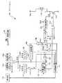
次に、ステーション100および電子時計200の電気的構成について説明する。
<ステーション>
まず、ステーション100側の構成について図3を参照して説明する。この図に示すように、ステーション側コイル110の一方の端子は、電源電圧Vccにプルアップされる一方、その他方の端子Dは、トランジスタ153のドレインに接続される。ここで、トランジスタ153のゲートは、一方の入力端にクロック信号CLKの供給を受けるアンドゲート152の出力と接続される一方、トランジスタ153のソースは接地されている。
ここで、クロック信号CLKは、各部の動作を同期させるための信号であり、発振回路140により生成されるものである。
【0023】
さて、充電開始ボタン1031および通信開始ボタン1032は、ユーザによって押下されると、それぞれ1ショットのパルス信号を出力するものである。ここで、両ボタンによって出力されるパルス信号を、説明の便宜上、総称してSTRとするが、いずれかのボタンが押下されたのかを区別するため、充電開始ボタン1031が押下された場合には、パルス信号CSが出力されるものとする。
次に、タイマA141は、パルス信号STRの供給を受けると、プリセット値mをクロック信号CLKでダウンカウントして、カウント動作中には、Hレベルとなる信号aを出力するものである。ここで、プリセット値mは、信号aのHレベル期間が、例えば10時間となるような値に設定されている。すなわち、タイマA141は、ユーザによって充電開始ボタン1031あるいは通信開始ボタン1032が押下されてから10時間だけHレベルとなる信号aを出力するように構成されている。そして、この信号aは、反転回路143によりレベル反転されて、オアゲート157の第2入力端と処理回路130とに供給されている。
また、タイマB142は、パルス信号STRの供給を受けると、プリセット値nをクロック信号CLKでダウンカウントして、カウント動作中には、Hレベルとなる信号bを出力するものである。ここで、プリセット値nは、mよりも十分に小さく設定されており、信号bのHレベル期間が、例えば30分となるような値に設定されている。すなわち、タイマB142は、ユーザによって充電開始ボタン1031あるいは通信開始ボタン1032の一方が押下されてから、30分だけHレベルとなる信号bを出力するように構成されている。
【0024】
ここで、タイマA141による設定時間は、フル充電状態に相当する容量まで充電するのに十分な時間であって、充電開始ボタン1031あるいは通信開始ボタン1032が押下された後に、何らかの理由によって、後述するコマンドcom3が電子時計200から送出されない場合でも、充電を終了させる目的で設定されるものである。
また、タイマB142による設定時間は、電池容量がゼロの状態からデータ転送可能状態(システム起動状態)となるまで充電するのに要する時間であって、(1)電子時計200がステーション100に収容されているが、電池容量が十分でないため、データ転送可能な状態にない場合である、あるいは、(2)電子時計200がステーション100に収容されていない場合である、のかを判別するのを目的として設定されるものである。
次に、コマンド検出器160は、パルス信号STRの供給を受けた後に、信号bがHレベルとなる30分の一定期間において、電子時計200側から後述するコマンドcom1〜com3を受信していない場合にHレベルとなる信号dを出力するものである。そして、この信号dは、オアゲート157の第1入力端と処理回路130とに供給されている。なお、このコマンド検出器160の詳細構成については後述する。
【0025】
ところで、充電・転送切換器170は、パルス信号STRの供給を受けた後、信号OFFがLレベルである期間において、図4(a)に示されるような第1充電信号をパルス信号eとして出力する一方、充電開始ボタン1031が押下されることによりパルス信号CSの供給を受けて、かつ、電子時計200側から後述するコマンドcom1を受信して信号com1の供給を受けると、図4(b)に示されるように、デューティ比を大きくした第2充電信号を信号eとして出力するものである。
ただし、充電・転送切換器170は、信号OFFがHレベルに遷移すると、信号eをLレベルに保持させる。
この充電・転送切換器170によって、トランジスタ153は、パルス信号STRの供給を受けた後、信号eがHレベルである期間において、クロック信号CLKのレベルに応じてドレイン−ソース間をスイッチングさせる構成となっている。このため、ステーション側コイル110には、電源電圧Vccをクロック信号CLKでスイッチングしたパルス信号が印加されるので、外部磁界が発生して、電子時計200を充電するようになっている。
一方、信号eがLレベル期間においては、アンドゲート152が閉じるので、ステーション側コイル110は、電源電圧Vccでプルアップされた状態となる。この状態において、時計側コイル210により外部磁界が発生すると、ステーション側コイル110の端子Dには、信号S2が誘起されることとなる。この信号S2は、受信回路154に供給される。受信回路154は、信号S2についてクロック信号CLKを用いて復調するものであり、その詳細構成については、後述する。次に、デコーダ155は、信号eがLレベルである期間において、受信回路154による復調結果をデコードするものである。
【0026】
したがって、信号eがHレベルである期間においては電子時計200の充電が行われる一方、信号eがLレベルである期間においてはデータ転送が行われることとなる。このため、充電・転送切換器170は、信号eのレベルによって、充電とデータ転送とを切り換える意義を有することになる。
さて、電子時計200からの信号は、後述するコマンドcom1〜com3のほか、脈拍数や心拍数などの生体情報(データ)などであり、デコーダ155は、生体情報については、処理回路130に供給する一方、各コマンドcom1〜com3を受信したことを、その出力信号com1〜com3をHレベルとすることで各部に通知する。 オアゲート156は、各信号com1〜com3の論理和を信号cとして出力するものである。このため、信号cは、電子時計200からコマンドcom1〜com3のいずれかを受信している状態を示す信号としての意義を有する。
ここで、デコード結果がコマンドcom1であることを示す信号com1は、充電・転送切換器170に供給されている。
また、デコード結果がコマンドcom2であることを示す信号com2は、ラッチ回路158を介して処理回路130に供給されている。
【0027】
さらに、デコード結果がコマンドcom3であることを示す信号com3は、オアゲート157の第3入力端に供給されている。そして、オアゲート157による論理和が信号OFFとして充電・転送切換器170に供給される。
ここで、オアゲート157の第1〜第3入力端に供給される信号は、第1に、コマンド検出器160による信号dと、第2に、タイマA141の信号aをレベル反転した信号と、第3に、デコード結果がコマンドcom3であることを示す信号com3とであるから、充電・転送切換器170は、次のいずれかに該当する場合に信号eの出力を終了するように構成されている。
すなわち、充電・転送切換器170が信号eをLレベルに保持して、充電を終了させる場合とは、(1)充電開始ボタン1031あるいは通信開始ボタン1032の押下によって信号STRが出力されてから30分の期間が経過するまで、電子時計200側からコマンドcom1〜com3を受信しない場合と、(2)充電が開始されてから10時間経過した場合と、(3)電子時計200から受信した信号がコマンドcom3である場合と、である。
なお、処理回路130は、入力された信号や、デコードされた生体情報などの各種表示を表示部104に実行させるためのものである。
【0028】
<コマンド検出器>
次に、コマンド検出器160の構成について図5を参照して説明する。
まず、アンドゲート1601は信号bおよび信号cの論理積を出力する。次に、ノアゲート1603および1604からなるRSフリップフロップは、アンドゲート1601の論理積をR信号として入力するとともに、信号STRをS信号として入力する。インバータ回路1605は、ノアゲート1604の出力を反転して信号U1として、Dフリップフロップ1606のD入力端に供給する。このDフリップフロップ1606は、信号STRでリセットするとともに、信号bの立ち下がりにおいて、その直前での入力端Dのレベルを信号dとして出力するものである。
さて、ユーザによって、充電開始ボタン1031あるいは通信開始ボタン1032が押下されると、1ショットのパルス信号STRが、例えば、図6(a)に示されるように出力される。この信号STRにより、ノアゲート1604の出力はLレベルとなるため、信号U1はHレベルとなる一方、タイマB142(図3参照)がカウント動作を実行するため、図6(a)に示されるように、信号bが一定期間だけHレベルとなる。
ここで、図3におけるデコーダ155が電子時計200からコマンドcom1〜com3を受信する場合、これらのコマンドは、信号eがLレベルの期間においてパルス的に出力される。
【0029】
このような場合において、信号bおよび信号cがともにHレベルとなって、その論理積がHレベルとなると、ノアゲート1604の出力はHレベルとなるから、信号U1はLレベルに遷移し、以降、この状態が保持される。したがって、1ショットのパルス信号STRが出力されてから一定時間経過して信号bが立ち下がった時点(正確にはその直前)において、Dフリップフロップ1606の出力端Qから出力される信号dは、Lレベルのままとなる。
一方、デコーダ155が電子時計200からコマンドcom1〜com3を受信しない場合、信号cは、図6(b)に示されるようにLレベルのままとなる。このため、信号U1はHレベルに保持されるので、信号STRが出力されてから一定時間経過して信号bが立ち下がった時点において、Dフリップフロップ1606の出力端Qから出力される信号dは、Hレベルに遷移する。
このように、コマンド検出器160は、パルス信号STRの供給を受けてから30分経過するまでの一定期間において、電子時計200側から少なくともコマンドcom1〜com3を受信すれば、期間経過後に信号dをHレベルに遷移させる一方、いずれのコマンドも受信しなければ、信号dをLレベルに保持するように構成されている。
【0030】
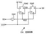
<受信回路>
次に、受信回路154の構成について図7を参照して説明する。なお、図示の構成はあくまでも一例であって、本来的に、データ転送における変調方式によって定められるものである。
まず、ステーション側コイル110における他方の端子Dに誘起された信号S2は、図7に示されるように、インバータ回路1541によってレベル反転されるとともに波形整形されて、発振回路140(図3参照)のクロック信号CLKと同期するDフリップフロップ1542、1543のリセット信号RSTとして供給される。ここで、Dフリップフロップ1542の入力端Dは、電源電圧Vccに接続される一方、その出力端Qは、次段のDフリップフロップ1543の入力端Dに接続される。そして、Dフリップフロップ1543の出力端Qが、復調結果たる信号S3として出力される構成となっている。
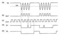
【0031】
次に、上記構成の受信回路154における各部の波形について検討してみる。電子時計200からのデータ受信時にあっては、トランジスタ153(図3参照)がスイッチングしないので、プルアップされたステーション側コイル110における他方の端子Dは、時計側コイル210による外部磁界が発生していなければプルアップレベルとなる一方、外部磁界が発生していれば、それに応じて誘起されるレベルにて変動する。このため、端子Dに誘起される信号S2は、例えば、図8(a)に示される通りとなる。
このような信号S2に対して、インバータ回路1541の出力たる信号RSTは、図8(b)に示されるように、信号S2の電圧がしきい値Vthを下回ったときにHレベルとなり、Dフリップフロップ1542、1543をリセットする。この際、Dフリップフロップ1542、1543は、クロック信号CLKの立ち上がりにおいて、その直前での入力端Dのレベルを出力するから、Dフリップフロップ1542の出力Q1、および、Dフリップフロップ1543の出力S3は、それぞれ図8(d)、(e)に示されるようになる。すなわち、受信回路154の出力信号S3は、時計側コイル210によって外部磁界が発生している期間にLレベルとなる信号となる。
ここで、時計側コイル210によって外部磁界が発生する期間とは、後述するように、電子時計200からステーション100へ転送されるデータがLレベルとなる期間であるから、結局、信号S3は、電子時計200からのデータやコマンドを復調したものであることが判る。
【0032】
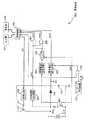
<電子時計>
次に、電子時計200の電気的構成について説明する。図9は、その構成を示すブロック図である。
この図に示されるように、時計側コイル210の一方の端子Pは、ダイオード245を介して二次電池220の正側端子に接続される一方、コイル210の他方の端子は、二次電池220の負側端子に接続されている。このため、ステーション側コイル110(図3参照)にパルス信号が印加されて、外部磁界が発生すると、その外部磁界により時計側コイル210の一方の端子Pに信号が誘起される。そして、この誘起信号は、トランジスタ253がオフのときにダイオード245によって整流されて二次電池220に充電される構成となっている。ここで、二次電池220の電圧Vccが、電子時計200における各部の電源として用いられる構成となっている。
【0033】
次に、充電期間検出回路261は、端子Pに外部磁界による信号が誘起されているか否かを検出するものであり、図10(a)に示されるように端子Pで信号が誘起されている場合には、同図(b)に示されるようにHレベルとなる信号CHRを出力する。また、タイミング作成回路271は、一定幅を有するパルスを一定間隔毎に生成して、アンドゲート272の一方の入力端に供給するものである。アンドゲート272の他方の入力端には、充電期間検出回路261による信号CHRが供給されているため、アンドゲート272は、端子Pに外部磁界による信号が誘起されている場合に閉じることになる。したがって、アンドゲート272の信号CKTは、図10(c)に示されるように、端子Pで信号が誘起されている場合に、一定幅を有するパルスが一定間隔毎に出力される形となる。
この信号CKTは、トランジスタ253のベースに供給されている。また、トランジスタ253のコレクタは抵抗254を介して端子Pに接続される一方、そのエミッタは接地されている。このため、トランジスタ253は、信号CKTがHレベルの場合に、コレクタ−エミッタ間がオンするように構成されている。
【0034】
ここで、トランジスタ253がオンになった場合、抵抗254による電圧降下によってコレクタの電位が時計側コイル210に流れる電流に応じて変動する。すなわち、時計側コイル210に流れる電流が大きいほど、コレクタの電位レベルは低下する。充電電流判定回路263は、コレクタの電位レベルと基準レベルとを比較して、時計側コイル210に流れる電流が基準レベルに対応するしきい値電流以上であれば、Hレベルとなる信号を出力するものである。ラッチ回路264は、充電電流判定回路263の出力信号を信号CKTの立ち下がりでラッチするもの、すなわち、トランジスタ253のオン期間において判別された充電電流の比較結果を出力するものである。
次に、アンドゲート281は、充電期間検出回路261の信号CHRと、ラッチ回路264のラッチ結果との論理積を求め、信号com1として出力するものである。
また、アンドゲート282は、充電期間検出回路261の信号CHRと、ラッチ回路264によるラッチ結果の反転結果との論理積を求め、信号com2として出力するものである。
【0035】
さらに、電池電圧検出回路265は、信号CKTがLレベルである期間(トランジスタ253がオフとなっている期間)における二次電池220の端子電圧を検出して、二次電池220が完全な充電状態(フル充電状態)となっているか否かを検出して、その検出結果が肯定的であれば、Hレベルとなる信号com3を出力するものである。
ここで、信号com1がHレベルである場合とは、端子Pに信号が誘起されている場合であって、かつ、時計側コイル210に流れる電流がしきい値以上である場合であるから、ステーション側コイル110と、時計側コイル210とがお互いに正しい位置で対向している状態を意味している。
また、信号com2がHレベルである場合とは、端子Pに信号が誘起されている場合であって、かつ、時計側コイル210に流れる電流がしきい値未満である場合であるから、ステーション側コイル110と、時計側コイル210とがお互いに正しい位置で対向していない、すなわち、位置ずれしている状態を意味する。
さらに、信号com3がHレベルである場合とは、二次電池220がフル充電状態であって、これ以上充電する必要がない状態を意味する。
【0036】
次に、制御回路230は、計時機能を備える一種の中央処理制御装置であり、主に、次の処理を実行するものである。すなわち、制御回路230は、第1に、通常では、入力部203(図1では図示省略)で設定されたモードに応じた表示(例えば、現在時刻表示など)を、表示部204に実行させる機能と、第2に、端子Pに信号が誘起されて信号CHRがHレベルに遷移すると、各信号com1〜com3で示される状態を認識して、これらの各状態に対応するコマンドcom1〜com3を作成して、信号CHRがLレベルに遷移したときに送出する機能と、第3に、コマンドcom1〜com3の送出後、ステーション100へ送信すべきディジタルデータを出力する機能とを有する。ここで、制御回路230は、コマンドcom1〜com3やディジタルデータなどをW1として送信回路250に供給する。なお、ステーション100へ送信すべきディジタルデータとしては、図示しないセンサ等により計測された脈拍数や心拍数などの生体情報などが想定される。
送信回路250は、ステーション100へ送信すべきデータやコマンドなどをシリアル化するとともに、シリアルデータがLレベルである期間において、一定周波数の信号をバーストしたスイッチング信号を出力するものである。送信回路250によるスイッチング信号は、抵抗251を介してトランジスタ252のベースに供給される。また、同トランジスタのコレクタは、二次電池220の正側端子に接続される一方、同トランジスタのエミッタは、コイル210の一方の端子Pに接続されている。
【0037】
したがって、このような電子時計200にあっては、図10(a)に示されるように端子Pに信号が誘起されると、図10(b)に示されるように、信号が誘起されている期間に信号CHRはHレベルとなるとともに、図10(c)に示されるように、信号CKTが出力される。そして、図10(d)に示されるように、端子Pに信号が誘起されている場合であって、信号CKTがLレベルである場合に、二次電池220の充電が行われる一方、図10(e)に示されるように、端子Pに信号が誘起されている場合であって、信号CKTがHレベルである場合に、トランジスタ253がオンして、二次電池220への充電電流がチェックされる。さらに、図10(f)に示されるように、端子Pに信号が誘起されずに、信号CHRがLレベルとなる場合に、コマンドcom1〜com3やディジタルデータなどが転送されるようになっている。
【0038】
<コマンドやディジタルデータの転送動作>
次に、ステーション100および電子時計200におけるコマンドやディジタルデータの転送の動作について説明する。上述したように、電子時計200の充電動作は、信号eがHレベルである期間において行われるが、転送動作は、信号eがLレベルにおいて行われる。
まず、信号eがLレベルである期間においては、ステーション側コイル110には、パルス信号が印加されない。このため、ステーション側コイル110による外部磁界が発生しないから、時計側コイル210の端子Pには信号が誘起されないため、信号CHRはLレベルとなる。信号CHRがLレベルとなると、制御回路230は、コマンドcom1〜com3の送出に続き、ステーション100へ送信すべきデータを送信回路250に供給するため、電子時計200からステーション100への信号送信が開始されることになる。
ここで、送信回路250は、ステーション100への送信すべきデータがHレベルであれば、出力をHレベルとし、データがLレベルであれば一定周波数のパルス信号をバーストさせたものとするから、トランジスタ252は、送信すべきデータがHレベルである期間において、スイッチングすることとなる。
したがって、時計側コイル210には、ステーション100への送信すべきデータがLレベルである期間において、パルス信号が印加されることとなり、これによって外部磁界が発生することとなる。
この外部磁界によって、ステーション側コイル110の端子Dに、当該パルス信号と同周期の信号が誘起されることとなる。ここで、信号が誘起されている期間では、上記構成の受信回路154によって信号S3がLレベルとなり、それ以外は、Hレベルであるから、結局、ステーション100側では、電子時計200からのディジタルデータW1を復調した信号S3が得られることとなる。そして、デコーダ155は、信号S3をデコードして、その結果が生体情報等のディジタルデータあれば、処理回路130に供給する一方、コマンドcom1〜com3であれば、それに対応した信号com1〜com3を出力する。
このように、ステーション100は、電子時計200からのコマンドやディジタルデータを得ることができるようになっている。
【0039】
<充電・データ転送の動作>
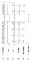
次に、ステーション100および電子時計200の充電・データ転送の動作について、図3および図9のブロック図とともに、図11のフローチャートを参照して説明する。
まず、ユーザは、電子時計200をステーション100の凹部101に収容させる。これにより、ステーション側コイル110と時計側コイル210とは、図2に示されるように互いに対向するため、電磁的に結合した状態となる。
この後、ユーザによって充電開始ボタン1031が押下されると、通信中か否かが判別される(ステップS1)。
ステップS1の判別において、通信中である場合には(ステップS1;Yes)、一旦充電待機状態となる(ステップS2)。
次に通信が終了したか否かを判別する(ステップS3)。
ステップS3の判別において、通信が終了していない場合には(ステップS3;No)、再び処理をステップS2に移行して充電待機状態を継続する。
ステップS1の判別において、非通信中である場合(ステップS1;No)、あるいは、ステップS3の判別において、通信が終了している場合(ステップS3;Yes)には、パルス信号STRによって、タイマA141およびタイマB142がカウント動作を開始する(ステップS4)。
また、パルス信号STRによって、充電・転送切換器170は、図4(a)に示されるような第1充電信号を信号eとして出力し、充電を行う(ステップS5)。
【0040】
次に、タイマA141がカウント動作を終了したか否かが、信号aの反転信号によって判別される(ステップS6)。
ステップS6の判別において、カウント動作が終了していれば(ステップS6;Yes)、それは、充電開始ボタン1031あるいは通信開始ボタン1032が押下されてから10時間以上経過したことを意味する。
上述したように、タイマA141による設定時間は、二次電池220をフル充電状態に相当する容量まで充電するのに十分な時間であるから、この設定時間を経過する前に、通常では、フル充電である旨を示すコマンドcom3の受信によって充電が終了するはずである。にもかかわらず、タイマA141による設定時間が経過したことは、二次電池220の故障などのような異常が発生していること意味する。
このため、処理回路130は、例えば、図12(c)に示されるような表示を表示部104に対して行わせて、その旨をユーザに告知する(ステップS7)。また、信号aの反転信号により信号OFFがHレベルとなるので、充電・転送切換器170は、信号eをLレベルに保持する。このため、異常が発生している場合において、電子時計200の充電は終了することになる(ステップS8)。
一方、タイマA141がカウント動作を終了していなければ(ステップS6;No)、現在の電池容量で通信が可能か否かを判別する(ステップS9)。
ステップS9の判別において、現在の電池容量では、通信不可能な場合には、処理を再びステップS5に移行し、充電・転送切換器170は、パルス信号STRによって、図4(a)に示されるような第1充電信号を信号eとして出力して充電を行い(ステップS5)、現在の電池容量で通信可能となるまで充電を継続する。
【0041】
ステップS9の判別において、現在の電池容量で通信可能となった場合には(ステップS9;Yes)、二次電池220がフル充電状態であるか否かが、電池電圧検出回路265によって判別される(ステップS10)。
ステップS10の判別において、フル充電状態であれば(ステップS10;Yes)、信号com3がHレベルである場合に相当し、上述したように、これ以上充電する必要がない状態である。そこで、制御回路230は、この状態をステーション100に通知すべく、コマンドcom3を送出し(ステップS11)、充電処理を終了する(ステップS12)。
また、ステップS10の判別において、フル充電状態でなければ(ステップS10;No)、信号com1がHレベルである場合に相当するから、上述したように、ステーション側コイル110と時計側コイル210とがお互いに正しい位置で対向しており、充電が良好に進行している状態である。そこで、制御回路230は、この状態をステーション100に通知すべく、コマンドcom1を送出する(ステップS13)。
そして、通信開始ボタン1032が押されたか否かを判別する(ステップS14)。
ステップS14の判別において、通信開始ボタン1032が押されなかった場合には(ステップS14;No)、処理を再びステップS6に移行し、同様の処理を繰り返す。
【0042】
ステップS14の判別において、通信開始ボタン1032が押された場合には(ステップS14;Yes)、充電を一時停止し(ステップS15)、コマンドcom1に続いて送出されたディジタルデータが受信回路154によって受信され、デコーダ155によってデコードされて、処理回路130にデータ転送される(ステップS16)。
そしてデータ転送が終了すると(ステップS17)、充電が一時停止中か否かを判別する(ステップS18)。
ステップS18の判別において、充電が一時停止中である場合には(ステップS18;Yes)、処理を再びステップS6に移行し、同様の処理を繰り返す。
ステップS18の判別において、充電が一時停止中では無い場合には(ステップS18;No)、転送が完了すると、処理回路130は、例えば、図12(d)に示されるような表示を表示部104に対して行わせるとともに(ステップS19)、受信したディジタルデータに基づく表示を表示部104に行わせて処理を終了する(ステップS20)。
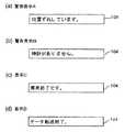
なお、ステーション側コイル110と時計側コイル210とが正しく対向しておらず、位置ずれしている場合には、それが検出されるとともに、その旨の警告が図12(a)に示されるように表示される。また、電子時計200がステーション100に収容されていないにもかかわらず、充電開始あるいはデータ転送が指示された場合には、それが検出されるとともに、その旨の警告が図12(b)に示されるように表示される。
【0043】
<変形例>
上記実施形態にあっては、次のような変形が可能である。
すなわち、実施形態におけるデータ転送は、電子時計200からステーション100への一方向のみであったが、ステーション100から電子時計200への方向であっても良いのはもちろんである。電子時計200へデータ転送する場合、ステーション100では、転送すべきデータに応じて変調する一方、電子時計200では、その変調方式に合わせて復調する構成とすれば良い。この際、変調・復調は、公知の技術を適用すれば良い。
【0044】
また、上記実施形態では、第1の機器としてステーション100、第2の機器あるいは相手方機器として電子時計200を例にとって説明したが、本願ではこれらの区別は本質的に無意味であり、電力転送や信号転送を行うすべての電子機器に適用可能である。例えば、電動歯ブラシや、電動ひげ剃り、コードレス電話、携帯電話、パーソナルハンディフォン、モバイルパソコン、PDA(Personal Digital Assistants:個人向情報端末)などの二次電池を備える被充電機器と、その充電機器とに適用可能である。
【0045】
以上の実施形態においては、電池残量(蓄電電圧)に基づいて充電制御を行っていたが、充電時間に基づいて制御を行うように構成することも可能である。
この場合には、所定時間以上充電がなされれば、通信可能であるというように判別すればよい。
【0046】
以上の実施形態においては、通信及び充電を行うための系として電磁誘導系、電磁結合系を用いていたが、赤外線等の光を用いた光学系を用いるように構成することも可能である。
【0047】
【発明の効果】
以上説明したように本発明によれば、携帯電子機器やその充電機器などのように、二つの電子機器間において、同一の系を介して充電及び通信を行う場合に、通信動作中に充電動作の開始が指示された場合には、通信動作に支障をきたさず、かつ、ユーザに面倒な操作の手間をかけることなく充電を行うことが可能となる。
また、充電動作中に通信動作の開始が指示された場合には、システムの安定性を確保しつつ通信を行うことが可能となる。
【図面の簡単な説明】
【図1】 本発明の実施形態にかかるステーションおよび電子時計の構成を示す平面図である。
【図2】 同ステーションおよび同電子時計の構成を示す断面図である。
【図3】 同ステーションの電気的構成を示すブロック図である。
【図4】 (a)および(b)は、それぞれ同ステーションにおける信号eたる第1および第2充電信号の波形を示す図である。
【図5】 同ステーションにおけるコマンド検出器の構成を示すブロック図である。
【図6】 (a)および(b)は、同コマンド検出器の動作を説明するためのタイミングチャートである。
【図7】 同ステーションの受信回路の一例を示す回路図である。
【図8】 (a)〜(e)は、それぞれ同受信回路の動作を説明するためのタイミングチャートである。
【図9】 同電子時計の電気的構成を示すブロック図である。
【図10】 (a)〜(f)は、それぞれ同電子時計における動作を説明するためのタイミングチャートである。
【図11】 同ステーションおよび同電子時計の間における充電・データ転送の動作を示すフローチャートである。
【図12】 (a)〜(d)は、それぞれ同ステーションにおける表示部の表示の一例を示す図である。
【符号の説明】
100……ステーション、
104……表示部、
110……ステーション側コイル、
130……処理回路、
153……トランジスタ、
154……受信回路、
200……電子時計、
210……時計側コイル、
220……二次電池、
245……ダイオード、
250……送信回路、
254……抵抗[0001]
BACKGROUND OF THE INVENTION
The present invention relates to an electronic device and a method for controlling the electronic device, and more particularly to an electronic device capable of performing communication and charging with another electronic device via the same system and a method for controlling the electronic device.
[0002]
[Prior art]
In recent years, small portable electronic devices such as portable terminals and electronic watches are housed in chargers called stations, and data transfer and the like are being performed along with charging of the portable electronic devices. Here, if it is configured to perform charging, data transfer, and the like via electrical contacts, these contacts are exposed, which causes a problem in terms of waterproofness. Therefore, it is desirable that charging, signal transfer, and the like be performed in a non-contact manner by electromagnetic coupling of coils disposed in both the station and the portable electronic device or optical coupling such as infrared communication.
[0003]
[Problems to be solved by the invention]
In such a configuration, if charging and communication are performed sequentially, if an instruction for the other operation is given by the user during the charging operation or communication operation, a new instruction will be issued regardless of the operation status of the operation before the instruction. Control is performed so as to shift to the performed operation.
According to such control, the response to the user's operation is good, but the following problems occur.
More specifically, if a charging operation is instructed during a communication operation, the communication will be forcibly terminated during the communication, and the program or data will not be transferred completely, resulting in a hindrance to the operation. There was a bug that it was.
[0004]
In addition, when the control is performed so as to ignore the charging, the charging start instruction must be performed again after the communication operation is finished, which causes a problem that the operation becomes complicated.
In addition, if the communication operation is instructed during the charging operation, if the battery capacity is low, the system operation lower limit voltage will be interrupted during the communication, and the operation of the system itself will become unstable if the operation shifts to the communication operation. The problem of becoming will arise.
Or, even if the communication is completed, the operation is completed with a low battery capacity, so that it is forced to be used in a low battery capacity state or the charging operation has to be performed again.
Accordingly, an object of the present invention is to continue charging or communication via the same system while maintaining a response to a user's operation between two or more devices separated from each other such as a portable electronic device or a station. Another object of the present invention is to provide an electronic device that can operate normally and a method for controlling the electronic device.
[0005]
[Means for Solving the Problems]
In order to achieve the above object, the configuration according to
[0006]
According to a second aspect of the present invention, in the electronic device according to the first aspect, when the control unit is further instructed to communicate with the other electronic device during charging of the other electronic device, the charging is performed. And the instructed communication is started, and charging is resumed after the communication is completed.
[0007]
According to a third aspect of the present invention, in the electronic device according to the first aspect, during the set time, the other electronic device can communicate with a secondary battery provided in the other electronic device from a state where the remaining battery level is zero. It is characterized by the time required to charge to the state.
[0013]
According to a fourth aspect of the present invention, in the electronic device according to any one of the first to third aspects, the same system is an optical system, an electromagnetic coupling system, or an electromagnetic induction system.
[0014]
The configuration according to claim 5 is between another electronic device.Without going through electrical contacts A method of controlling an electronic device that performs communication and charging through the same system, and when instructed to charge the other electronic device, whether or not communication with the other electronic device is in progress If the determination result is being communicated, charging is refrained until the end of the communication, whereas if the determination result is not being communicated, the charging period and the non-charging period are repeated alternately. Charging to another electronic device is started, and at least a signal indicating that charging is instructed within a predetermined set time and charging is not required from the other electronic device is received. If not, the charging period is set as the first amount of time, and when the signal indicating that charging is performed without any problem is received from the other electronic device, the charging period is set as the first amount of time. Greater than the second It is characterized in that change between amount.
[0019]
DETAILED DESCRIPTION OF THE INVENTION
Hereinafter, an embodiment of the present invention will be described. In the present embodiment, a station is used as the first device, and an electronic timepiece charged by the station as the second device will be described as an example. However, the present invention is not limited to these.
<Mechanical configuration>
FIG. 1 is a plan view illustrating a configuration of a station and an electronic timepiece according to the embodiment. As shown in this figure, the
Further, the
[0020]
2 is a cross-sectional view taken along line AA in FIG. As shown in this figure, a watch-
On the other hand, in the
Thus, in the state where the
[0021]
The
[0022]
<Electrical configuration>
Next, the electrical configuration of the
<Station>
First, the configuration on the
Here, the clock signal CLK is a signal for synchronizing the operation of each unit, and is generated by the
[0023]
Now, charging
Next, when the
When the
[0024]
Here, the set time by the
The set time by the
Next, after receiving the supply of the pulse signal STR, the
[0025]
By the way, after receiving the supply of the pulse signal STR, the charging /
However, the charge /
The charge /
On the other hand, when the signal e is at the L level, the AND
[0026]
Therefore, the
A signal from the
Here, the signal com1 indicating that the decoding result is the command com1 is supplied to the charge /
The signal com2 indicating that the decoding result is the command com2 is supplied to the
[0027]
Further, the signal com3 indicating that the decoding result is the command com3 is supplied to the third input terminal of the
Here, the signals supplied to the first to third input terminals of the
That is, the case where the charge /
The
[0028]
<Command detector>
Next, the configuration of the
First, the AND
Now, the charging
Here, when the
[0029]
In such a case, when both the signal b and the signal c become the H level and the logical product thereof becomes the H level, the output of the NOR
On the other hand, when the
As described above, if the
[0030]
<Receiver circuit>
Next, the configuration of the receiving
First, as shown in FIG. 7, the signal S2 induced at the other terminal D in the station-
[0031]
Next, the waveform of each part in the receiving
In contrast to such a signal S2, the signal RST output from the
Here, the period in which the external magnetic field is generated by the watch-
[0032]
<Electronic watch>
Next, the electrical configuration of the
As shown in this figure, one terminal P of the
[0033]
Next, the charging
This signal CKT is supplied to the base of the
[0034]
Here, when the
Next, the AND
The AND
[0035]
Further, the battery
Here, the case where the signal com1 is at the H level is a case where a signal is induced at the terminal P and the current flowing through the
The case where the signal com2 is at the H level is a case where a signal is induced at the terminal P and the current flowing through the
Furthermore, the case where the signal com3 is at the H level means that the
[0036]
Next, the
The
[0037]
Therefore, in such an
[0038]
<Command and digital data transfer operation>
Next, a command and digital data transfer operation in the
First, during the period in which the signal e is at the L level, no pulse signal is applied to the
Here, if the data to be transmitted to the
Therefore, a pulse signal is applied to the
By this external magnetic field, a signal having the same cycle as the pulse signal is induced at the terminal D of the
As described above, the
[0039]
<Charging and data transfer operations>
Next, the charging and data transfer operations of the
First, the user accommodates the
Thereafter, the charging
If it is determined in step S1 that communication is in progress (step S1; Yes), the battery is temporarily in a charging standby state (step S2).
Next, it is determined whether or not the communication has ended (step S3).
If it is determined in step S3 that communication has not ended (step S3; No), the process proceeds to step S2 again to continue the charge standby state.
If it is determined in step S1 that communication is not being performed (step S1; No), or if it is determined in step S3 that communication has been completed (step S3; Yes), the
Further, in response to the pulse signal STR, the charging /
[0040]
Next, it is determined by the inverted signal of the signal a whether or not the
In step S6, if the counting operation is completed (step S6; Yes), it is indicated by the
As described above, the set time by the
Therefore, for example, the
On the other hand, if the
If it is determined in step S9 that communication is not possible with the current battery capacity, the process returns to step S5, and the charge /
[0041]
In the determination of step S9, when communication is possible with the current battery capacity (step S9; Yes), the battery
If it is determined in step S10 that the battery is fully charged (step S10; Yes), this corresponds to the case where the signal com3 is at the H level, and as described above, it is not necessary to charge any more. Therefore, the
In step S10, if the battery is not fully charged (step S10; No), this corresponds to the case where the signal com1 is at the H level. Therefore, as described above, the
Then, a
In the determination of step S14, the
[0042]
In the determination of step S14, the
When the data transfer ends (step S17), it is determined whether or not the charging is temporarily stopped (step S18).
If it is determined in step S18 that charging is temporarily stopped (step S18; Yes), the process proceeds to step S6 again, and the same process is repeated.
If it is determined in step S18 that charging is not temporarily stopped (step S18; No), when the transfer is completed, the
In addition, when the
[0043]
<Modification>
In the above embodiment, the following modifications are possible.
That is, the data transfer in the embodiment is only in one direction from the
[0044]
In the above embodiment, the
[0045]
In the above embodiment, charging control is performed based on the remaining battery level (storage voltage), but it is also possible to perform control based on the charging time.
In this case, what is necessary is just to discriminate | determine that it is communicable if it performs charge more than predetermined time.
[0046]
In the above embodiment, an electromagnetic induction system and an electromagnetic coupling system are used as a system for performing communication and charging. However, an optical system using light such as infrared light may be used.
[0047]
【The invention's effect】
As described above, according to the present invention, when charging and communication are performed via the same system between two electronic devices, such as a portable electronic device and a charging device thereof, the charging operation is performed during the communication operation. When the start of the operation is instructed, it is possible to perform charging without causing trouble in the communication operation and without troublesome troublesome operation for the user.
In addition, when the start of the communication operation is instructed during the charging operation, it is possible to perform communication while ensuring the stability of the system.
[Brief description of the drawings]
FIG. 1 is a plan view showing configurations of a station and an electronic timepiece according to an embodiment of the present invention.
FIG. 2 is a cross-sectional view showing configurations of the station and the electronic timepiece.
FIG. 3 is a block diagram showing an electrical configuration of the station.
FIGS. 4A and 4B are diagrams showing waveforms of first and second charging signals which are signals e in the same station, respectively.
FIG. 5 is a block diagram showing a configuration of a command detector in the station.
FIGS. 6A and 6B are timing charts for explaining the operation of the command detector.
FIG. 7 is a circuit diagram showing an example of a receiving circuit of the station.
FIGS. 8A to 8E are timing charts for explaining the operation of the receiving circuit, respectively.
FIG. 9 is a block diagram showing an electrical configuration of the electronic timepiece.
FIGS. 10A to 10F are timing charts for explaining the operation of the electronic timepiece.
FIG. 11 is a flowchart showing charging / data transfer operations between the station and the electronic timepiece;
FIGS. 12A to 12D are diagrams showing examples of display on the display unit in the same station. FIG.
[Explanation of symbols]
100 …… Station,
104 …… Display section
110 …… Station side coil,
130 …… Processing circuit,
153: Transistor,
154 ....... receiving circuit,
200 …… Electronic watch,
210 …… Clock on the watch side,
220 …… Secondary battery,
245 ... Diode,
250 …… Transmission circuit,
254 …… Resistance
Claims (5)
Translated fromJapanese前記他の電子機器を充電することが指示された場合に、前記他の電子機器と通信中であるか否かを判別する判別手段と、
前記判別手段による判別結果が通信中であった場合は、当該通信が終わるまで充電の実行を控える一方、前記判別結果が通信中でなかった場合は、充電期間と非充電期間を交互に繰り返しながら前記他の電子機器に対する充電を開始し、少なくとも充電が指示されてから予め定められた設定時間内であって、かつ前記他の電子機器から充電する必要がない状態にあることを示す信号を受信していない場合は、前記充電期間を第1の時間量とする一方、前記他の電子機器から充電が支障なく行われていることを示す信号を受信すると、前記充電期間を前記第1の時間量よりも大きい第2の時間量に変更する制御手段と
を備えることを特徴とする電子機器。An electronic device that performs communication and charging through the same systemwithout using electrical contacts with other electronic devices,
A discriminating means for discriminating whether or not communication with the other electronic device is in progress when an instruction to charge the other electronic device is given;
If the determination result by the determination means is in communication, the charging is refrained until the communication is completed, while if the determination result is not in communication, the charging period and the non-charging period are alternately repeated. Charging to the other electronic device is started, and at least a signal indicating that charging is instructed within a predetermined set time and charging is not required from the other electronic device is received. If not, the charging period is set to the first amount of time, and when the signal indicating that charging is performed without any problem is received from the other electronic device, the charging period is set to the first time period. An electronic device comprising: control means for changing to a second time amount larger than the amount.
前記制御手段は、さらに、前記他の電子機器の充電中に前記他の電子機器と通信を行うことが指示されると、充電を中断して前記指示された通信を開始し、当該通信を終えた後に充電を再開することを特徴とする電子機器。The electronic device according to claim 1,
When the control unit is further instructed to communicate with the other electronic device during charging of the other electronic device, the control unit interrupts charging and starts the instructed communication, and ends the communication. The electronic device is characterized in that charging is resumed after a short time.
前記設定時間は、前記他の電子機器に備わる二次電池を、電池残量がゼロの状態から前記他の電子機器が通信可能となる状態まで充電するのに要する時間であることを特徴とする電子機器。The electronic device according to claim 1,
The set time is a time required to charge a secondary battery provided in the other electronic device from a state where the remaining battery level is zero to a state where the other electronic device can communicate. Electronics.
前記同一の系は、光学系、電磁結合系あるいは電磁誘導系であることを特徴とする電子機器。The electronic device according to any one of claims 1 to 3,
The electronic system is characterized in that the same system is an optical system, an electromagnetic coupling system, or an electromagnetic induction system.
前記他の電子機器を充電することが指示された場合に、前記他の電子機器と通信中であるか否かを判別し、
判別結果が通信中であった場合は、当該通信が終わるまで充電の実行を控える一方、
前記判別結果が通信中でなかった場合は、充電期間と非充電期間を交互に繰り返しながら前記他の電子機器に対する充電を開始し、
少なくとも充電が指示されてから予め定められた設定時間内であって、かつ前記他の電子機器から充電する必要がない状態にあることを示す信号を受信していない場合は、前記充電期間を第1の時間量とする一方、前記他の電子機器から充電が支障なく行われていることを示す信号を受信すると、前記充電期間を前記第1の時間量よりも大きい第2の時間量に変更する
ことを特徴とする電子機器の制御方法。A method for controlling an electronic device that performs communication and charging via the same systemwithout using an electrical contact with another electronic device,
When it is instructed to charge the other electronic device, it is determined whether the communication with the other electronic device is in progress,
If the determination result is in communication, while charging is stopped until the communication ends,
If the determination result is not in communication, start charging the other electronic device while alternately repeating the charging period and the non-charging period,
If the signal indicating that charging is not required from the other electronic device is received within at least a predetermined set time after the charging is instructed, the charging period is When a signal indicating that charging is performed without any problem from the other electronic device is received, the charging period is changed to a second amount of time that is greater than the first amount of time. A method for controlling an electronic device.
Priority Applications (1)
| Application Number | Priority Date | Filing Date | Title |
|---|---|---|---|
| JP27996899AJP3777908B2 (en) | 1999-09-30 | 1999-09-30 | Electronic device and control method of electronic device |
Applications Claiming Priority (1)
| Application Number | Priority Date | Filing Date | Title |
|---|---|---|---|
| JP27996899AJP3777908B2 (en) | 1999-09-30 | 1999-09-30 | Electronic device and control method of electronic device |
Publications (2)
| Publication Number | Publication Date |
|---|---|
| JP2001102974A JP2001102974A (en) | 2001-04-13 |
| JP3777908B2true JP3777908B2 (en) | 2006-05-24 |
Family
ID=17618456
Family Applications (1)
| Application Number | Title | Priority Date | Filing Date |
|---|---|---|---|
| JP27996899AExpired - Fee RelatedJP3777908B2 (en) | 1999-09-30 | 1999-09-30 | Electronic device and control method of electronic device |
Country Status (1)
| Country | Link |
|---|---|
| JP (1) | JP3777908B2 (en) |
Cited By (1)
| Publication number | Priority date | Publication date | Assignee | Title |
|---|---|---|---|---|
| CN104104156A (en)* | 2013-04-08 | 2014-10-15 | 索尼公司 | Electronic unit and power feeding system |
Families Citing this family (22)
| Publication number | Priority date | Publication date | Assignee | Title |
|---|---|---|---|---|
| JP5247215B2 (en) | 2008-04-04 | 2013-07-24 | キヤノン株式会社 | COMMUNICATION DEVICE AND ITS CONTROL METHOD |
| JP4725610B2 (en)* | 2008-07-16 | 2011-07-13 | セイコーエプソン株式会社 | Power transmission control device, power transmission device, power reception control device, power reception device, and electronic device |
| US8929957B2 (en)* | 2008-11-21 | 2015-01-06 | Qualcomm Incorporated | Reduced jamming between receivers and wireless power transmitters |
| JP5593926B2 (en) | 2010-07-29 | 2014-09-24 | ソニー株式会社 | Power feeding system, power feeding device and electronic device |
| US8983374B2 (en)* | 2010-12-13 | 2015-03-17 | Qualcomm Incorporated | Receiver for near field communication and wireless power functionalities |
| JP6064337B2 (en) | 2011-08-10 | 2017-01-25 | ソニー株式会社 | Power feeding system, power feeding device and electronic device |
| JP6007561B2 (en) | 2011-10-21 | 2016-10-12 | ソニー株式会社 | Power supply device and power supply system |
| JP6003172B2 (en) | 2011-10-21 | 2016-10-05 | ソニー株式会社 | Power supply device and power supply system |
| JP2013102665A (en) | 2011-10-21 | 2013-05-23 | Sony Corp | Power-feed device and power-feed system |
| JP5919991B2 (en) | 2011-11-29 | 2016-05-18 | ソニー株式会社 | Electronic device, power supply device and power supply system |
| JP6060516B2 (en) | 2011-11-30 | 2017-01-18 | ソニー株式会社 | Electronic equipment and power supply system |
| JP5849842B2 (en) | 2011-12-21 | 2016-02-03 | ソニー株式会社 | Power supply device, power supply system, and electronic device |
| JP5857861B2 (en) | 2011-12-21 | 2016-02-10 | ソニー株式会社 | Power supply device, power supply system, and electronic device |
| JP6060515B2 (en) | 2011-12-22 | 2017-01-18 | ソニー株式会社 | Electronic equipment and power supply system |
| JP6047911B2 (en) | 2011-12-22 | 2016-12-21 | ソニー株式会社 | Electronic equipment and power supply system |
| US9722451B2 (en) | 2012-01-27 | 2017-08-01 | Sony Corporation | Electronic unit and power feeding system |
| JP5847651B2 (en)* | 2012-06-01 | 2016-01-27 | 株式会社東芝 | Power receiving device and power transmitting / receiving system |
| JP2014030288A (en) | 2012-07-31 | 2014-02-13 | Sony Corp | Power-feeding device and power-feeding system |
| JP5836898B2 (en)* | 2012-08-01 | 2015-12-24 | ルネサスエレクトロニクス株式会社 | Communication apparatus and operation method thereof |
| JP6040899B2 (en) | 2013-04-08 | 2016-12-07 | ソニー株式会社 | Electronic equipment and power supply system |
| JP6677795B2 (en)* | 2016-02-24 | 2020-04-08 | ローム株式会社 | Wireless power transmission device, control method thereof, power transmission control circuit, charger |
| EP3926787B1 (en) | 2016-10-12 | 2024-05-22 | Snap Inc. | Circuits and methods for wearable device charging and wired control |
- 1999
- 1999-09-30JPJP27996899Apatent/JP3777908B2/ennot_activeExpired - Fee Related
Cited By (2)
| Publication number | Priority date | Publication date | Assignee | Title |
|---|---|---|---|---|
| CN104104156A (en)* | 2013-04-08 | 2014-10-15 | 索尼公司 | Electronic unit and power feeding system |
| CN104104156B (en)* | 2013-04-08 | 2019-06-28 | 索尼公司 | Electronic unit and feed system |
Also Published As
| Publication number | Publication date |
|---|---|
| JP2001102974A (en) | 2001-04-13 |
Similar Documents
| Publication | Publication Date | Title |
|---|---|---|
| JP3777908B2 (en) | Electronic device and control method of electronic device | |
| JP3826407B2 (en) | Electronic device, electronic device control method, secondary battery capacity estimation method, and secondary battery charge control method | |
| TW480759B (en) | Electronic machine, charged electronic machine and control method of electronic machine | |
| JP3747677B2 (en) | Electronics | |
| JP3794267B2 (en) | Electronics | |
| JP2549192B2 (en) | Non-contact IC card and method of using the same | |
| JP2011229265A (en) | Non-contacting power transmitter | |
| JPH09219932A (en) | Charging device for wireless equipment | |
| CN107615612A (en) | Controls, electronics and contactless power transmission systems | |
| JPH03262089A (en) | Noncontact type ic card | |
| US7265520B2 (en) | Electronic apparatus and method of controlling the electronic apparatus | |
| JP3888060B2 (en) | Electronic device and control method of electronic device | |
| JP4067595B2 (en) | Non-contact charging device compatible with multiple devices | |
| JP3659020B2 (en) | Method for estimating capacity of electronic device and secondary battery | |
| JP3622700B2 (en) | Electronic device and control method of electronic device | |
| JP2000270486A (en) | Electronic device, communication system including the electronic device, and control method of the communication system | |
| JPH11275774A (en) | Electronic device and charge control method | |
| JP3843641B2 (en) | Electronics | |
| JPH07114536B2 (en) | Rechargeable electronic device | |
| JP2001285171A (en) | Relay device, signal relay system, and control method of relay device | |
| JP3206244B2 (en) | Cordless telephone | |
| JPH01157232A (en) | Charging device for electronic watches | |
| JPH11274989A (en) | Communication method, communication device, and electronic device | |
| CN218940782U (en) | Magnetic attraction wireless charger | |
| JP2001021985A (en) | Charging device and camera system |
Legal Events
| Date | Code | Title | Description |
|---|---|---|---|
| A131 | Notification of reasons for refusal | Free format text:JAPANESE INTERMEDIATE CODE: A131 Effective date:20050816 | |
| A521 | Request for written amendment filed | Free format text:JAPANESE INTERMEDIATE CODE: A523 Effective date:20051017 | |
| A131 | Notification of reasons for refusal | Free format text:JAPANESE INTERMEDIATE CODE: A131 Effective date:20051115 | |
| A521 | Request for written amendment filed | Free format text:JAPANESE INTERMEDIATE CODE: A523 Effective date:20060111 | |
| TRDD | Decision of grant or rejection written | ||
| A01 | Written decision to grant a patent or to grant a registration (utility model) | Free format text:JAPANESE INTERMEDIATE CODE: A01 Effective date:20060207 | |
| A61 | First payment of annual fees (during grant procedure) | Free format text:JAPANESE INTERMEDIATE CODE: A61 Effective date:20060220 | |
| R150 | Certificate of patent or registration of utility model | Free format text:JAPANESE INTERMEDIATE CODE: R150 Ref document number:3777908 Country of ref document:JP Free format text:JAPANESE INTERMEDIATE CODE: R150 | |
| FPAY | Renewal fee payment (event date is renewal date of database) | Free format text:PAYMENT UNTIL: 20090310 Year of fee payment:3 | |
| FPAY | Renewal fee payment (event date is renewal date of database) | Free format text:PAYMENT UNTIL: 20100310 Year of fee payment:4 | |
| FPAY | Renewal fee payment (event date is renewal date of database) | Free format text:PAYMENT UNTIL: 20100310 Year of fee payment:4 | |
| FPAY | Renewal fee payment (event date is renewal date of database) | Free format text:PAYMENT UNTIL: 20110310 Year of fee payment:5 | |
| FPAY | Renewal fee payment (event date is renewal date of database) | Free format text:PAYMENT UNTIL: 20120310 Year of fee payment:6 | |
| FPAY | Renewal fee payment (event date is renewal date of database) | Free format text:PAYMENT UNTIL: 20120310 Year of fee payment:6 | |
| FPAY | Renewal fee payment (event date is renewal date of database) | Free format text:PAYMENT UNTIL: 20130310 Year of fee payment:7 | |
| FPAY | Renewal fee payment (event date is renewal date of database) | Free format text:PAYMENT UNTIL: 20140310 Year of fee payment:8 | |
| S531 | Written request for registration of change of domicile | Free format text:JAPANESE INTERMEDIATE CODE: R313531 | |
| R350 | Written notification of registration of transfer | Free format text:JAPANESE INTERMEDIATE CODE: R350 | |
| LAPS | Cancellation because of no payment of annual fees |