JP3775410B2 - Laser processing method, laser welding method and laser processing apparatus - Google Patents
Laser processing method, laser welding method and laser processing apparatusDownload PDFInfo
- Publication number
- JP3775410B2 JP3775410B2JP2003369929AJP2003369929AJP3775410B2JP 3775410 B2JP3775410 B2JP 3775410B2JP 2003369929 AJP2003369929 AJP 2003369929AJP 2003369929 AJP2003369929 AJP 2003369929AJP 3775410 B2JP3775410 B2JP 3775410B2
- Authority
- JP
- Japan
- Prior art keywords
- laser
- optical element
- diffractive optical
- processing
- laser beam
- Prior art date
- Legal status (The legal status is an assumption and is not a legal conclusion. Google has not performed a legal analysis and makes no representation as to the accuracy of the status listed.)
- Expired - Fee Related
Links
- 238000012545processingMethods0.000titleclaimsdescription78
- 238000003466weldingMethods0.000titleclaimsdescription45
- 238000000034methodMethods0.000titleclaimsdescription21
- 238000003672processing methodMethods0.000titleclaimsdescription4
- 230000003287optical effectEffects0.000claimsdescription100
- 229910000679solderInorganic materials0.000claimsdescription38
- 239000000758substrateSubstances0.000claimsdescription31
- 230000008569processEffects0.000claimsdescription8
- 230000001678irradiating effectEffects0.000claimsdescription5
- 239000013078crystalSubstances0.000description11
- 230000008859changeEffects0.000description4
- 238000004519manufacturing processMethods0.000description4
- 239000003990capacitorSubstances0.000description3
- 238000013461designMethods0.000description3
- 238000003754machiningMethods0.000description3
- 238000012986modificationMethods0.000description3
- 230000004048modificationEffects0.000description3
- 238000010586diagramMethods0.000description2
- 230000000694effectsEffects0.000description2
- 239000010453quartzSubstances0.000description2
- VYPSYNLAJGMNEJ-UHFFFAOYSA-Nsilicon dioxideInorganic materialsO=[Si]=OVYPSYNLAJGMNEJ-UHFFFAOYSA-N0.000description2
- 238000005476solderingMethods0.000description2
- 230000009471actionEffects0.000description1
- 238000004220aggregationMethods0.000description1
- 230000002776aggregationEffects0.000description1
- 238000005275alloyingMethods0.000description1
- 238000007796conventional methodMethods0.000description1
- 230000007423decreaseEffects0.000description1
- 238000009826distributionMethods0.000description1
- 238000005553drillingMethods0.000description1
- 238000001312dry etchingMethods0.000description1
- 238000005516engineering processMethods0.000description1
- 238000002474experimental methodMethods0.000description1
- 238000010438heat treatmentMethods0.000description1
- 239000000463materialSubstances0.000description1
- 238000002844meltingMethods0.000description1
- 230000008018meltingEffects0.000description1
- 229920002120photoresistant polymerPolymers0.000description1
- 229920000642polymerPolymers0.000description1
- 238000006116polymerization reactionMethods0.000description1
- 230000005855radiationEffects0.000description1
- 239000004065semiconductorSubstances0.000description1
Images


Classifications
- H—ELECTRICITY
- H05—ELECTRIC TECHNIQUES NOT OTHERWISE PROVIDED FOR
- H05K—PRINTED CIRCUITS; CASINGS OR CONSTRUCTIONAL DETAILS OF ELECTRIC APPARATUS; MANUFACTURE OF ASSEMBLAGES OF ELECTRICAL COMPONENTS
- H05K3/00—Apparatus or processes for manufacturing printed circuits
- H05K3/30—Assembling printed circuits with electric components, e.g. with resistor
- H05K3/32—Assembling printed circuits with electric components, e.g. with resistor electrically connecting electric components or wires to printed circuits
- H05K3/34—Assembling printed circuits with electric components, e.g. with resistor electrically connecting electric components or wires to printed circuits by soldering
- H05K3/3494—Heating methods for reflowing of solder
- B—PERFORMING OPERATIONS; TRANSPORTING
- B23—MACHINE TOOLS; METAL-WORKING NOT OTHERWISE PROVIDED FOR
- B23K—SOLDERING OR UNSOLDERING; WELDING; CLADDING OR PLATING BY SOLDERING OR WELDING; CUTTING BY APPLYING HEAT LOCALLY, e.g. FLAME CUTTING; WORKING BY LASER BEAM
- B23K1/00—Soldering, e.g. brazing, or unsoldering
- B23K1/005—Soldering by means of radiant energy
- B23K1/0056—Soldering by means of radiant energy soldering by means of beams, e.g. lasers, E.B.
- B—PERFORMING OPERATIONS; TRANSPORTING
- B23—MACHINE TOOLS; METAL-WORKING NOT OTHERWISE PROVIDED FOR
- B23K—SOLDERING OR UNSOLDERING; WELDING; CLADDING OR PLATING BY SOLDERING OR WELDING; CUTTING BY APPLYING HEAT LOCALLY, e.g. FLAME CUTTING; WORKING BY LASER BEAM
- B23K26/00—Working by laser beam, e.g. welding, cutting or boring
- B23K26/02—Positioning or observing the workpiece, e.g. with respect to the point of impact; Aligning, aiming or focusing the laser beam
- B23K26/04—Automatically aligning, aiming or focusing the laser beam, e.g. using the back-scattered light
- B23K26/042—Automatically aligning the laser beam
- B—PERFORMING OPERATIONS; TRANSPORTING
- B23—MACHINE TOOLS; METAL-WORKING NOT OTHERWISE PROVIDED FOR
- B23K—SOLDERING OR UNSOLDERING; WELDING; CLADDING OR PLATING BY SOLDERING OR WELDING; CUTTING BY APPLYING HEAT LOCALLY, e.g. FLAME CUTTING; WORKING BY LASER BEAM
- B23K26/00—Working by laser beam, e.g. welding, cutting or boring
- B23K26/02—Positioning or observing the workpiece, e.g. with respect to the point of impact; Aligning, aiming or focusing the laser beam
- B23K26/06—Shaping the laser beam, e.g. by masks or multi-focusing
- B23K26/067—Dividing the beam into multiple beams, e.g. multifocusing
- B23K26/0676—Dividing the beam into multiple beams, e.g. multifocusing into dependently operating sub-beams, e.g. an array of spots with fixed spatial relationship or for performing simultaneously identical operations
- H—ELECTRICITY
- H05—ELECTRIC TECHNIQUES NOT OTHERWISE PROVIDED FOR
- H05K—PRINTED CIRCUITS; CASINGS OR CONSTRUCTIONAL DETAILS OF ELECTRIC APPARATUS; MANUFACTURE OF ASSEMBLAGES OF ELECTRICAL COMPONENTS
- H05K2203/00—Indexing scheme relating to apparatus or processes for manufacturing printed circuits covered by H05K3/00
- H05K2203/10—Using electric, magnetic and electromagnetic fields; Using laser light
- H05K2203/107—Using laser light
Landscapes
- Physics & Mathematics (AREA)
- Optics & Photonics (AREA)
- Engineering & Computer Science (AREA)
- Mechanical Engineering (AREA)
- Plasma & Fusion (AREA)
- Manufacturing & Machinery (AREA)
- Microelectronics & Electronic Packaging (AREA)
- Laser Beam Processing (AREA)
Description
Translated fromJapanese本発明は、レーザーを利用した加工に関し、例えば、プリント基板上に回路部品を、レーザーを使ってはんだ溶接し(特に鉛フリーはんだ溶接)、実装する方法等に関する。 The present invention relates to processing using a laser, for example, a method of mounting a circuit component on a printed circuit board by soldering using a laser (particularly lead-free solder welding) and the like.
レーザーを用いてはんだ溶接を行いプリント基板上に各種部品(水晶振動子、IC、抵抗、コンデンサ等)を実装する方法が知られている。それらの各種部品がプリント基板へはんだ溶接によって接続される際、各部品はその接続端子を介して接続されるが、その接続端子の配置は各部品毎に、その向きや間隔が様々である。そのため、従来は、1本のレーザービームをはんだが盛られた接合個所に照射し、部品を移動させるかあるいはレーザービームを走査することにより複数の接合箇所で順次溶接を行って、各部品をプリント基板に接続させていた(例えば、特許文献1乃至4参照)。 There is known a method of mounting various parts (quartz crystal oscillator, IC, resistor, capacitor, etc.) on a printed board by performing solder welding using a laser. When these various components are connected to the printed circuit board by solder welding, each component is connected via its connection terminal, and the arrangement and the interval of the connection terminal vary for each component. For this reason, conventionally, a laser beam is irradiated onto a soldered joint, and the parts are moved or scanned by a laser beam to perform welding sequentially at a plurality of joints and print each part. It was connected to the substrate (see, for example,
しかし、従来の方法には次のような問題があった。すなわち、レーザービームを目的の加工(溶接を含む)個所へ照射するには、部品を載せたステージを移動及び回転させる必要がある。しかし、このようなステージ制御を量産ラインで採用することは実用的ではない。重量のあるステージを、加工個所の向きや間隔に合わせて小刻みに加速減速移動させることは困難だからである。現実には、実装部品ならびに基板は一方向にだけ流れるように供給されることがほとんどである。
一方において、上記の問題は、ガルバノミラーでビームを走査すれば回避される。しかし、その場合には、ガルバノミラー及びその制御ソフトに要するコストに加え、同ミラーを配置する空間が必要になり、これらは量産装置の簡略化を阻む要因となる。また、複数の加工個所をレーザービームの照射により順次加熱するため、同時に照射加熱する場合と比べて加工に要する時間が増し、その間に生じる放熱のために光利用効率が低下するという問題もあった。However, the conventional method has the following problems. That is, in order to irradiate the target processing (including welding) location with the laser beam, it is necessary to move and rotate the stage on which the component is placed. However, it is not practical to use such stage control in a mass production line. This is because it is difficult to accelerate and decelerate a heavy stage in small increments according to the direction and interval of the machining location. In reality, the mounting component and the substrate are mostly supplied so as to flow in only one direction.
On the other hand, the above problem can be avoided by scanning the beam with a galvanometer mirror. However, in that case, in addition to the cost required for the galvanometer mirror and its control software, a space for arranging the mirror is required, which becomes a factor that prevents simplification of the mass production apparatus. In addition, since a plurality of processing points are sequentially heated by laser beam irradiation, the time required for processing is increased as compared with the case of simultaneous irradiation heating, and there is a problem that light utilization efficiency decreases due to heat radiation generated during that time. .
本発明は、上記課題に対処するためになされたもので、電子部品等の各種部品の基板への実装に際して必要とされるそれら部品の基板への接続を、簡便な構成でより効率的に実施できるレーザー溶接方法及び装置を得ることを目的とする。また、この溶接方法と同じ原理を被加工物の他の加工、例えば除去加工または改質加工等の一般加工にも応用して、それらの加工に際してレーザーの照射位置決めが容易に実施できるレーザー加工方法及び装置を得ることも目的としている。 The present invention has been made in order to address the above-described problems, and more efficiently implements the connection of various components such as electronic components to the substrate, which are required for mounting on the substrate, with a simple configuration. An object of the present invention is to obtain a laser welding method and apparatus. In addition, the same principle as this welding method is applied to other processing of the workpiece, for example, general processing such as removal processing or modification processing, and laser processing method that can easily carry out laser irradiation positioning in those processing And also to obtain a device.
本発明のレーザー加工方法は、1本のレーザービームを回折光学素子により回折して、0次の回折次数のレーザービームを端部に含んだほぼ等強度の複数のレーザービームからなるビーム列に分岐する工程と、前記ビーム列からなる集光スポット列を前記0次のレーザービームを中心として、被加工物の複数の加工ポイントの列方向へ合わせて回転させる方向設定工程と、前記回折光学素子から前記被加工物までの距離を調節して、前記集光スポット列のスポット間隔を前記複数の加工ポイントの間隔に合わせる間隔設定工程と、前記集光スポット列の方向とスポット間隔が定められた前記複数のレーザービームの強度を加工に必要な強度まで増大して、該ビームを前記複数の加工ポイントに同時に照射し前記被加工物を加工する工程とを備え、前記回折光学素子を通過した0次のレーザービームと前記加工ポイントの一つを一致させた後、前記各設定工程を実行する。これによれば、被加工物の溶接、除去または改質等の加工において以下のような効果を奏する。
(1)簡便な光学系で一つの加工列の複数個所を同時に加工できる。
(2)回折光学素子の回転と高さの調整だけで、複数の加工ポイントの方向及び間隔が異なる加工列毎の加工に容易に対応できる。
(3)加工部位周囲の実装部品に対する熱影響を排除できる。
(4)量産用の加工装置が簡略化できる。In the laser processing method of the present invention, one laser beam is diffracted by a diffractive optical element, and is branched into a beam array composed of a plurality of laser beams of substantially equal intensity including a zero-order diffraction order laser beam at the end. And a direction setting step of rotating the condensing spot array composed of the beam array around the zero-order laser beam in accordance with the array direction of a plurality of processing points of the workpiece, and from the diffractive optical element An interval setting step of adjusting the distance to the workpiece to adjust the spot interval of the focused spot row to the interval of the plurality of processing points, and the direction of the focused spot row and the spot interval are determined. A step of increasing the intensity of a plurality of laser beams to an intensity necessary for processing, and simultaneously irradiating the plurality of processing points with the plurality of processing points to process the workpiece. , After the diffractive optical element and the 0-order laser beam passing through the matched one of the working point, to perform the respective setting step. According to this, the following effects are exhibited in processing such as welding, removal or modification of the workpiece.
(1) A plurality of locations in one processing row can be processed simultaneously with a simple optical system.
(2) By simply adjusting the rotation and height of the diffractive optical element, it is possible to easily cope with processing for each processing row in which the directions and intervals of a plurality of processing points are different.
(3) The influence of heat on the mounted parts around the processing site can be eliminated.
(4) A processing apparatus for mass production can be simplified.
本発明のレーザー溶接方法は、1本のレーザービームを回折光学素子により回折して、0次の回折次数のレーザービームを端部に含んだほぼ等強度の複数のレーザービームからなるビーム列に分岐する工程と、前記ビーム列からなる集光スポット列を前記0次のレーザービームを中心として、基板に実装された部品の前記基板との複数の溶接ポイントの列方向へ合わせて回転させる方向設定工程と、前記回折光学素子から前記基板までの距離を調節して、前記集光スポット列のスポット間隔を前記複数の溶接ポイントの間隔に合わせる間隔設定工程と、前記集光スポット列の方向とスポット間隔が定められた前記複数のレーザービームの強度を溶接に必要な強度まで増大して、該ビームを前記複数の溶接ポイントに同時に照射し前記基板と前記部品を接続する工程とを備え、前記回折光学素子を通過した0次のレーザービームと前記溶接ポイントの一つを一致させた後、前記各設定工程を実行する。これにより、部品の基板への実装においても、上記(1)〜(4)と同様の効果が得られる。 In the laser welding method of the present invention, one laser beam is diffracted by a diffractive optical element, and is branched into a beam array composed of a plurality of laser beams having substantially equal intensities including a zero-order diffraction order laser beam at the end. And a direction setting step of rotating the condensing spot array composed of the beam array in accordance with the array direction of a plurality of welding points with the substrate of the component mounted on the substrate with the zeroth-order laser beam as the center. Adjusting the distance from the diffractive optical element to the substrate to adjust the spot interval of the focused spot row to the interval of the plurality of welding points, and the direction and spot interval of the focused spot row And increasing the intensity of the plurality of laser beams determined to the intensity required for welding, and simultaneously irradiating the plurality of welding points to the substrate and the substrate. And a step of connecting the components, after the diffractive optical element 0-order laser beam passing through the a match of one of the welding point, to perform the respective setting step. As a result, the same effects as in the above (1) to (4) can be obtained in mounting the component on the board.
上記方法においては、前記回折光学素子を通過した0次のレーザービームと前記加工ポイントの一つを一致させた後、前記各設定工程を実行するのが好ましい。これによれば、集光スポット列の方向及びそのスポット間隔の設定に引き続いて、直ちに部品の加工や溶接が実行できるので、作業性と正確性が向上する。なお、溶接は、はんだ、特に鉛フリーはんだを用いたはんだ溶接としてもよい。 In the above method, it is preferable to execute each of the setting steps after making the zero-order laser beam that has passed through the diffractive optical element coincide with one of the processing points. According to this, subsequent to the setting of the direction of the focused spot row and the setting of the spot interval, parts can be processed and welded immediately, so that workability and accuracy are improved. The welding may be solder welding, particularly solder welding using lead-free solder.
本発明のレーザー加工装置は、レーザー発振器と、前記レーザー発振器から出射された1本のレーザービームを、0次の回折次数のレーザービームを端部に含んだほぼ等強度の複数のレーザービームからなるビーム列に分岐する回折光学素子と、前記回折光学素子をその光軸を中心として所望の角度回転させる回転装置と、前記回折光学素子をその光軸方向に所望の距離移動させる移動装置と、を備えたものである。これによれば、レーザー加工装置が簡便に構成でき、しかも、複数の加工ポイントが一定の間隔で一定の方向にある場合にはそれらの加工ポイントを同時に加工できる。また、それらの方向及び間隔が異なる別の加工列の加工も、回折光学素子の回転と高さ調整だけで容易に対応できる。
The laser processing apparatus according to the present invention includes a laser oscillator and a plurality of laser beams of substantially equal intensity including one laser beam emitted from the laser oscillator and a zero-order diffraction order laser beam at the end. A diffractive optical element that branches into a beam train; a rotating device that rotates the diffractive optical element by a desired angle about its optical axis; and a moving device that moves the diffractive optical element by a desired distance in the optical axis direction. It is provided. According to this, the laser processing apparatus can be simply configured, and when a plurality of processing points are in a constant direction at a constant interval, the processing points can be processed simultaneously. Further, processing of other processing rows having different directions and intervals can be easily handled only by rotating the diffractive optical element and adjusting the height.
また、前記回折光学素子に入射するレーザービームを該回折光学素子と一体にそれらの光軸方向に対して直角方向に動かす光軸位置決め装置を備えてもよい。これによれば、回折光学素子で分岐された0次のレーザービームを、任意の加工ポイントに一致させることができるので、加工の基準位置決めが容易となり、従って、被加工物の異なる領域における加工列の加工に容易に移行できる。 Further, an optical axis positioning device that moves the laser beam incident on the diffractive optical element in a direction perpendicular to the optical axis direction integrally with the diffractive optical element may be provided. According to this, since the zeroth-order laser beam branched by the diffractive optical element can be made to coincide with an arbitrary processing point, the processing reference positioning is facilitated, and therefore processing rows in different regions of the workpiece are processed. It can easily shift to processing.
さらに、被加工物上のレーザー照射部位にはんだを供給するはんだディスペンサを備えてもよい。これにより、はんだ溶接の作業効率が向上する。 Furthermore, you may provide the solder dispenser which supplies a solder to the laser irradiation site | part on a to-be-processed object. Thereby, the work efficiency of solder welding improves.
本発明においては、回折光学素子により分岐された複数のレーザービーム(分岐ビーム)の集光スポットからなる列(集光スポット列)の中に必ず0次ビームを含める。0次ビームは、分岐ビーム列の向きや長さに関係なく、光軸上に集光するため、その回折光学素子を回転させ、あるいはその高さを変えても、常に加工面上の同じ場所に位置することになる。このことを利用し、回折光学素子により生じた分岐ビーム列を、その0次ビームの位置を基準にしてその向きと長さを容易に調整することができる。この点に着目して成されたのが本発明である。なお、本発明では、0次ビームを任意の高次ビームと組み合わせることが可能である。以下、本発明をその実施形態に即して詳細に説明する。 In the present invention, the zero-order beam is always included in a row (condensed spot row) composed of the condensed spots of a plurality of laser beams (branched beams) branched by the diffractive optical element. Since the zero-order beam is focused on the optical axis regardless of the direction and length of the branched beam train, it is always the same location on the processing surface even if its diffractive optical element is rotated or its height is changed. Will be located. By utilizing this fact, the direction and length of the branched beam train generated by the diffractive optical element can be easily adjusted with reference to the position of the zero-order beam. The present invention has been made paying attention to this point. In the present invention, the zero-order beam can be combined with any higher-order beam. Hereinafter, the present invention will be described in detail according to the embodiment.
図1は本発明の実施形態に係るレーザー加工装置の基本構成図である。このレーザー加工装置は、レーザーを発生するレーザー発振器1と、レーザー発振器1から出力されたレーザービーム2を集光する集光装置としての集光レンズ3と、集光レンズ3により集光された1本のレーザービーム2を回折して複数の分岐ビーム2Aを生成する位相格子等の回折光学素子4と、回折光学素子4を光軸を中心にその光軸と直交する面内で回転させる回転装置5と、回折光学素子4をその光軸方向に移動(ここでは上下移動)させる移動装置6とを備える。ここで、回転装置5としてはθステージ、移動装置6としてはZステージ等、既に良く知られた装置が使用できる。 FIG. 1 is a basic configuration diagram of a laser processing apparatus according to an embodiment of the present invention. This laser processing apparatus includes a
さらに、レーザー加工装置は、レーザー発振器1またはその後段に配置されるレーザー照射ヘッド(図示せず)から回折光学素子4までの光学系を、それらの光軸方向に対して直角方向に移動させる、光軸位置決め装置8を備えるのが好ましい。また、必要に応じて、レーザー照射部位にはんだを供給するはんだディスペンサ9を備えても良い。なお、上記集光装置は、レンズに限定されるものではなく、レーザーを集光できる他の素子から構成してもよい。 Further, the laser processing apparatus moves the optical system from the
次に、上記加工装置の作用を説明する。なお、ここでは、加工に用いる2本の分岐ビームが、図2に示すような回折次数と光強度を有するように予め設計した回折光学素子4を備えているものとする。レーザー発振器1から出射されたレーザービーム2は集光レンズ3で集光され回折光学素子4に入る。回折光学素子4は、入射した1本のレーザービームを図2に示すような複数の分岐ビームにして射出し、これらの複数の分岐ビームの集光スポットから成る集光スポット列をつくる。 Next, the operation of the processing apparatus will be described. Here, it is assumed that the two branched beams used for processing include a diffractive
ここまでにおいては、回折光学素子4により形成された集光スポット列は、被加工物に予定されている複数の加工ポイントからなる方向と一致していないし、また、集光スポット列のスポット間隔もそれら加工ポイントの間隔に一致していない。そこで、次に、以下の調整を行う。 Up to this point, the condensing spot row formed by the diffractive
まず、回折光学素子4を通過した0次のレーザービームを、被加工物7に予定されている複数の加工ポイントからなる列(加工ポイント列)を構成する一つの加工ポイントに合わせる基準位置決めを行う。続いて、図3に示すように、回折光学素子4を光軸と直交する面内でその光軸を中心に回転させるさせると集光スポット列が回転することを利用し、回転装置5により回折光学素子4をその面内で光軸を中心に回転させて、集光スポット列を被加工物7の加工ポイント列の方向と一致させる。例えば、回折光学素子4をその光軸を中心に角度θ回転させると、集光スポット列も角度θだけ回転する。この操作により、+1次の分岐ビームによる集光スポットは、図5の矢印Aのように移動する。 First, reference positioning is performed so that the 0th-order laser beam that has passed through the diffractive
続いて、図4に示すように、移動装置6を利用して、回折光学素子4から被加工物7の加工面(又は溶接面)7Aまでの距離を変えて、分岐ビーム列の集光スポット間隔を加工ポイント列の間隔に合わせる。この操作により、+1次の分岐ビームによる集光スポットは、図5の矢印Bのように移動する。以上の図3及び図4に説明した調整により、回折光学素子4で分岐された複数の分岐ビームによる集光スポット列の方向と間隔は、複数の加工ポイントによる加工ポイント列のそれらと一致する。 Subsequently, as shown in FIG. 4, by using the moving device 6, the distance from the diffractive
回折光学素子4に関して上記の各調整を行うことで、回折光学素子4により分岐された分岐ビームの集光スポット列の各スポットを、被加工物7の列状に並んだ複数の加工ポイントの各ポイントに一致させることができる。なお、先に、集光スポット列の方向と間隔を各加工ポイントのそれらに対応させておき、その後、0次あるいは他の次数の集光スポットを基準として、各集光スポットと各加工ポイントを一致させることも可能である。しかし、先に、回折光学素子4を通過した0次のレーザービームによる集光スポットと加工ポイントの一つを一致させ、その後、集光スポット列の方向と間隔を加工ポイント列のそれらに一致させる方が、その後の作業性や加工の正確性の点からは好ましい。 By performing each of the adjustments described above with respect to the diffractive
ここで、図4を基に、回折光学素子4から被加工物7の加工面7Aまでの光軸上の距離Zと、0次の分岐ビームによる集光スポットから+1次の分岐ビームによる集光スポットまでの間隔Δとの関係について説明する。距離Zと、間隔Δとの関係は、次の近似式で与えられる。
Δ=(Z/Zmax)Δmax …(1)
ここで、ZmaxはZの最大値、ΔmaxはΔの最大値である。例えば、Zmax=90mm、Δmax=1.1mmとすると、Zを0〜90mmの範囲で変えることにより、Δは0〜1.1mmの間で変化する。そして、この加工装置を基板への部品実装の際のはんだ(「はんだ」には「鉛フリーはんだ」を含む、以下の記載でも同じ)溶接に用いる場合、実用上は、Zを45〜90mmの範囲で変えるくらいが適当である。この場合、集光スポットの間隔Δは、0.55〜1.1mmまで変化する。これくらいの幅で調節できれば、基板への部品のはんだ溶接における用途には十分である。なお、さらに集光スポットの間隔Δを広げたい場合には、回折光学素子4から加工面7Aまでの間隔Zmaxを長くすればよい。逆に、集光スポットの間隔Δを狭めたい場合には、Zmaxを短くすればよい。Here, based on FIG. 4, the distance Z on the optical axis from the diffractive
Δ = (Z / Zmax) Δmax (1)
Here, Zmax is the maximum value of Z, and Δmax is the maximum value of Δ. For example, if Zmax = 90 mm and Δmax = 1.1 mm, Δ changes between 0 and 1.1 mm by changing Z in the range of 0 to 90 mm. And when this processing apparatus is used for soldering (“solder” includes “lead-free solder”, the same applies to the following description) welding when mounting components on the board, practically, Z is 45 to 90 mm. It is appropriate to change the range. In this case, the condensing spot interval Δ varies from 0.55 to 1.1 mm. If it can be adjusted to such a width, it is sufficient for use in solder welding of components to a substrate. In order to further increase the distance Δ between the focused spots, the distance Zmax from the diffractive
本実施の形態で用いた回折光学素子4は、その断面が鋸歯状の1次元レリーフ型格子である。それはフォトレジスト露光とドライエッチングにより、使用波長に対して十分に透明な石英基板上に形成される。この格子の周期dは、次式から求まる。
d=λZmax/Δmax …(2)
ここで、例えば、λ=0.808μm、Zmax=90mm、Δmax=1.1mmとすると、d=66.1μmとなる。さらに、この格子の回折次数毎のビーム強度は以下の式で与えられる。
I0=sin2(φ/2)/(φ/2)2…(3−1)
Im=sin2[(2πm−φ)/2]/[(2πm−φ)/2]2…(3−2)
ここで、I0とImは0次ビームの強度とm次ビームの強度である。φは格子の位相変調深さであり、φ=2πh(n−1)/λである。なお、nは材料の屈折率、hは格子の深さである。例えば、図1に示すように、ほぼ等強度の2本の分岐ビームを利用して加工を行う場合、その条件は、式(3−1)、(3−2)から、φ=πと導ける。そして、この場合、回折ビームの強度は以下のように求まる。
I0=(2/π)2 …(4−1)
Im=[2/(2m−1)π]2…(4−2)The diffractive
d = λZmax / Δmax (2)
Here, for example, if λ = 0.008 μm, Zmax = 90 mm, and Δmax = 1.1 mm, d = 66.1 μm. Further, the beam intensity for each diffraction order of the grating is given by the following equation.
I0 = sin2 (φ / 2) / (φ / 2)2 (3-1)
Im = sin2 [(2πm−φ) / 2] / [(2πm−φ) / 2]2 (3-2)
Here, I0 and Im are the intensity of the 0th order beam and the intensity of the mth order beam. φ is the phase modulation depth of the grating, and φ = 2πh (n−1) / λ. Note that n is the refractive index of the material, and h is the depth of the grating. For example, as shown in FIG. 1, when processing is performed using two branched beams having approximately equal intensities, the condition can be derived as φ = π from equations (3-1) and (3-2). . In this case, the intensity of the diffracted beam is obtained as follows.
I0 = (2 / π)2 (4-1)
Im = [2 / (2m−1) π]2 (4-2)
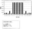
また、式(3−1)、(3−2)を用いて計算した回折ビームの次数と強度の関係を示したものが図2である。図2によれば、0次と+1の強度は等しく、0.405である。この他の強度は、−1次と+2次が等しく0.045、−2次と+3次が等しく0.016である。これより、はんだ溶接における光利用効率は81%となり、その値は実用上十分である。また、はんだ溶接に用いる0次及び+1次2本のビームとその他のビームとの強度比は0.405/0.045=9.0であり、はんだ溶接に要するビーム強度を考慮すると、0次及び+1次以外の回折ビームが接合部の周囲に損傷を与えることもない。 FIG. 2 shows the relationship between the order and intensity of the diffracted beam calculated using the equations (3-1) and (3-2). According to FIG. 2, the 0th and +1 intensities are equal, 0.405. The other intensities are equal to 0.045 for the −1st order and + 2nd order, and 0.016 for the −2nd order and + 3rd order. Thus, the light use efficiency in solder welding is 81%, which is practically sufficient. In addition, the intensity ratio of the 0th and + 1st order beams used for solder welding and the other beams is 0.405 / 0.045 = 9.0. And diffracted beams other than the + 1st order do not damage the periphery of the junction.
また、格子の設計に必要な格子の深さhは、次式から求まる。
h=φλ/[2π(n−1)]…(5)
ここで、φ=πであり、n=1.45とすると、h=0.898μmとなる。
なお、等強度の2本の分岐ビームを用いてはんだ溶接を行う場合の例を上に記したが、分岐ビーム間の強度比は回折光学素子の設計事項であり、必要に応じて変更することが可能である。Further, the depth h of the lattice necessary for the design of the lattice is obtained from the following equation.
h = φλ / [2π (n−1)] (5)
Here, if φ = π and n = 1.45, h = 0.898 μm.
In addition, although the example in the case of performing solder welding using two branch beams of equal intensity is described above, the intensity ratio between the branch beams is a design matter of the diffractive optical element and should be changed as necessary. Is possible.
図6は回路基板への水晶振動子の実装の方法を示す例示図である。ここで、水晶振動子10には2本の接続ピン11,12があり、これらのピン11,12を基板上でターミナル21,22に挿入してはんだ溶接により両者を接続する例である。実験に使用したターミナル21,22の間隔は0.80mmであり、それぞれの配線21A,22Aの幅は0.30mmであった。水晶振動子10の基板への接続は、まず、レーザー発振器1から基板やその基板上に実装されている部品に損傷を与えないような低い強度のレーザービームを出力する。そして、光軸位置決め装置8などを利用して、回折光学素子4を通過した0次のレーザービームによる集光スポットとターミナル21,22のいずれか一つを一致させる。続いて、すでに説明した方法で、回折光学素子4で生成された分岐ビーム2Aによる集光スポット列の方向と間隔を、ターミナル21,22の列方向と間隔に一致させる。
続いて、加工装置に並設されたはんだディスぺンサ9を利用してそれぞれのターミナル21,22の接続部位へはんだを供給する。次に、上記のようにして集光スポット列の位置、方向及び間隔がターミナル21,22の列のそれらと一致された2本の分岐ビーム2Aの強度を、レーザー発振器1の出力を調整して、目的の加工が可能な強度まで増大させる。ここでは、それらの分岐ビーム2Aがはんだを溶融できる強度まで増大させる。そしてその強度が増大された2本の分岐ビームをはんだが溶融するまで接続部位へ同時に照射し、接続ピン11,12とターミナル21,22とを溶接接続する。これにより水晶振動子10が基板に接続される。この方法によれば、独立した2個所で同時にはんだが加熱されるため、はんだの溶融と凝集が問題なく進む。特に、この例のように、はんだ溶接の個所が接近している場合、1本のビームで1個所づつ照射加熱すると、ビーム加熱されている側のはんだに反対側のはんだが融合し、配線が短絡する場合がある。この現象は、ビーム走査で交互にはんだを照射加熱した場合にも、走査速度が有限であるために起こり得るが、本実施形態によればそれも回避できる。FIG. 6 is an exemplary view showing a method of mounting a crystal resonator on a circuit board. Here, the
Subsequently, solder is supplied to the connection portions of the
なお、異なる複数の水晶振動子、抵抗、コンデンサ等が基板に実装される場合、それらの接続ターミナルの向きや間隔は基板上で一様ではない。その場合には、それぞれの水晶振動子、抵抗、コンデンサ等の実装個所毎に、上記集光スポット列の位置決めを行うことが必要となる。また、同じ種類の実装部品であってもピン間隔が異なるものが混在する場合には、回折光学素子と実装基板との距離を調節して、集光スポット列のスポット間隔を調整する必要がある。 When a plurality of different crystal resonators, resistors, capacitors, and the like are mounted on the substrate, the directions and intervals of their connection terminals are not uniform on the substrate. In that case, it is necessary to position the focused spot row for each mounting location of each crystal resonator, resistor, capacitor, and the like. In addition, even when the same type of mounting parts has different pin spacing, it is necessary to adjust the distance between the diffractive optical element and the mounting substrate to adjust the spot spacing of the focused spot array. .
以上は、回折光学素子の光分岐作用を利用して加工へ用いる2本のレーザービームを生じさせた例であるが、回折光学素子の設計により、所望の本数の加工用レーザービームを生じさせることもできる。例えば、図7は別の回折光学素子4Aにより生成された分岐ビームの回折次数と光強度の関係を示すグラフである。この回折光学素子4Aは、1本のレーザービームを分岐して0次から+6次までの7本の加工用レーザービームを等間隔で発生するようにしたものである。この場合、7本の分岐ビームによる光利用率は約85%、それらのビームの分岐均一性は約0.99となっており、十分に実用的な値となっている。なお、レーザービームの分岐数が3本以上の場合には、回折光学素子の形状は必ずしも鋸歯状とはならず、必要とされるレーザービームの分岐数及び分岐されたレーザービームの強度分布に応じて回折光学素子形状を設計する。従って、その素子形状の設計により、0次を含んだ正負どちらか一方の高次ビームを用いることも可能となるほか、光利用効率をさらに高めることも可能となる。 The above is an example in which two laser beams used for processing are generated by utilizing the light branching action of the diffractive optical element. By designing the diffractive optical element, a desired number of processing laser beams can be generated. You can also. For example, FIG. 7 is a graph showing the relationship between the diffraction order of a branched beam generated by another diffractive
図8は図7に示した回折光学素子4Aを用いて被加工物を加工する場合の例示図である。ここでは、片側7本の接続ピン31〜37を有するIC30を基板の対応するターミナル41〜47に挿入して、はんだ溶接により接続する例を示している。なお、図中、41A〜47Aは各ターミナルへの基板上の配線を示している。この場合も、まず、レーザー発振器1から基板やその基板上に実装されている部品に損傷を与えないような低い強度のレーザービームを出力する。そして、光軸位置決め装置8などを利用して、回折光学素子4Aを通過した0次のレーザービームによる集光スポットを、ターナル列を構成している一つのターミナル(ここでは左端のターミナル)41に一致させる。続いて、回折光素子4Aをその光軸を中心に回転させ、回折光学素子4Aにより生成された7本の分岐ビーム2Aによる集光スポット列を、ターミナル41〜47の列方向に一致させる。さらに、回折光学素子4Aを光軸方向に沿って移動させ、上記集光スポット列の間隔を、ターミナル41〜47のそれぞれの間隔に一致させる。続いて、それぞれのターミナル41〜47の接続部位へはんだを供給する。次に、上記のようにして集光スポット列の位置、方向及び間隔がターミナル41〜47の列のそれらと一致された7本の分岐ビーム2Aの強度を、レーザー発振器1の出力を調整して、はんだ溶接が可能な強度まで増大させる。そしてその強度が増大された7本の分岐ビーム2Aをはんだが溶融するまで接続部位へ同時に照射し、IC30の片側にある7つの接続ピン31〜37とターミナル41〜47とを溶接接続する。そして、IC30のもう一方側のピン列も、同様にして基板に接続する。これによれば、14カ所の溶接を非常に効率よくしかも周囲の部品に熱的影響を与えることなく実施することができる。 FIG. 8 is an exemplary view when a workpiece is processed using the diffractive
本発明のレーザー接合技術には、レーザー発振器として、例えば、YAGレーザー(波長1.064μm)や高出力半導体レーザー(波長0.808μm、0.940μm)等が使用できる。また、その他の加工においても、その加工特性に応じて、各種のレーザー発振器が利用できる。なお、上記実施形態では、レーザー発振器1の出力を変更することにより分岐ビーム2Aの強度を変更したが、レーザー発振器1の出力を固定し、発振器1の外部に配置したアッテネータ等、他のビーム強度変更手段を用いて、分岐ビーム2Aの強度を変更してもよい。さらに、上記実施形態で説明した1次元分岐ビームを用いた加工例を示したが、2次元分岐ビームを利用した加工にも本発明は適用可能である。 In the laser bonding technique of the present invention, for example, a YAG laser (wavelength 1.064 μm) or a high-power semiconductor laser (wavelengths 0.808 μm, 0.940 μm) can be used as a laser oscillator. Also, in other processing, various laser oscillators can be used depending on the processing characteristics. In the above embodiment, the intensity of the branched
本発明のレーザー加工技術は、回折光学素子により分岐される0次ビームと高次ビームの組み合わせに着目し、量産化の際の大きな課題である、分岐ビームと加工点の位置合わせを容易にしたものであり、本発明は加工点の並びの向き及び間隔が加工列毎に相違する場合に幅広く応用できる。従って、上記実施の形態で取り上げた実装部品のはんだ溶接は本発明の一応用例であって、それと異なる種々の加工、例えば、はんだ溶接以外の溶接加工、除去加工(孔開け、溝切り)、改質加工(合金化、高分子重合、屈折率変調)へも本発明は適用可能である。その場合、集光スポット列の位置、方向及び間隔が定められた複数の分岐ビームを、加工ポイントに同時に照射するレーザーの出力及び照射時間は、加工の種類に応じて適宜定めればよい。 The laser processing technology of the present invention has focused on the combination of the 0th order beam and the higher order beam branched by the diffractive optical element, and has facilitated the alignment of the branched beam and the processing point, which is a major issue in mass production. Therefore, the present invention can be widely applied when the direction and interval of the processing points are different for each processing row. Accordingly, the solder welding of the mounting component taken up in the above embodiment is an application example of the present invention, and various other processes such as welding processes other than solder welding, removal processes (drilling, grooving), and modification. The present invention can also be applied to quality processing (alloying, polymer polymerization, refractive index modulation). In that case, the output and irradiation time of a laser for simultaneously irradiating a processing point with a plurality of branched beams whose positions, directions, and intervals of the focused spot row are determined may be appropriately determined according to the type of processing.
1…レーザー発振器、2…レーザービーム、2A…分岐ビーム、3…集光レンズ、4,4A…回折光学素子、5…回転装置、6…移動装置、7…被加工物、7A…加工面、8…光軸位置決め装置、9…はんだディスペンサ、10…水晶振動子、11,12…水晶振動子の接続端子、21,22…基板の水晶振動子用ターミナル、30…IC、31〜37…ICの接続端子、41〜47…基板のIC用ターミナル。
DESCRIPTION OF
Claims (7)
Translated fromJapanese前記ビーム列からなる集光スポット列を前記0次のレーザービームを中心として、被加工物の複数の加工ポイントの列方向へ合わせて回転させる方向設定工程と、
前記回折光学素子から前記被加工物までの距離を調節して、前記集光スポット列のスポット間隔を前記複数の加工ポイントの間隔に合わせる間隔設定工程と、
前記集光スポット列の方向とスポット間隔が定められた前記複数のレーザービームの強度を加工に必要な強度まで増大して、該ビームを前記複数の加工ポイントに同時に照射し前記被加工物を加工する工程とを備え、
前記回折光学素子を通過した0次のレーザービームと前記加工ポイントの一つを一致させた後、前記各設定工程を実行することを特徴とするレーザー加工方法。Diffracting one laser beam by a diffractive optical element, and branching the beam into a beam array composed of a plurality of laser beams of substantially equal intensity including a laser beam of 0th diffraction order at the end;
A direction setting step of rotating the focused spot array composed of the beam array around the zero-order laser beam in accordance with the array direction of a plurality of processing points of the workpiece;
Adjusting the distance from the diffractive optical element to the workpiece, an interval setting step for adjusting the spot interval of the focused spot row to the interval of the plurality of processing points;
Increasing the intensity of the plurality of laser beams, the direction of the focused spot array and the spot interval being set, to an intensity necessary for processing, and simultaneously irradiating the plurality of processing points with the beam to process the workpiece. Comprising the steps of:
A laser processing method, wherein the setting steps are executed after the zero-order laser beam that has passed through the diffractive optical element is matched with one of the processing points.
前記ビーム列からなる集光スポット列を前記0次のレーザービームを中心として、基板に実装された部品の前記基板との複数の溶接ポイントの列方向へ合わせて回転させる方向設定工程と、
前記回折光学素子から前記基板までの距離を調節して、前記集光スポット列のスポット間隔を前記複数の溶接ポイントの間隔に合わせる間隔設定工程と、
前記集光スポット列の方向とスポット間隔が定められた前記複数のレーザービームの強度を溶接に必要な強度まで増大して、該ビームを前記複数の溶接ポイントに同時に照射し前記基板と前記部品を接続する工程とを備え、
前記回折光学素子を通過した0次のレーザービームと前記溶接ポイントの一つを一致させた後、前記各設定工程を実行することを特徴とするレーザー溶接方法。Diffracting one laser beam by a diffractive optical element, and branching the beam into a beam array composed of a plurality of laser beams of substantially equal intensity including a laser beam of 0th diffraction order at the end;
A direction setting step of rotating the condensing spot array composed of the beam array around the zero-order laser beam in accordance with the array direction of a plurality of welding points with the substrate of the component mounted on the substrate;
Adjusting the distance from the diffractive optical element to the substrate, an interval setting step for adjusting the spot interval of the focused spot row to the interval of the plurality of welding points;
Increasing the intensity of the plurality of laser beams, the direction of the focused spot row and the spot interval being set to those required for welding, simultaneously irradiating the plurality of welding points with the substrate and the component A process of connecting,
The laser welding method according to claim 1, wherein after the zero-order laser beam that has passed through the diffractive optical element is matched with one of the welding points, the setting steps are performed.
前記レーザー発振器から出射された1本のレーザービームを、0次の回折次数のレーザービームを端部に含んだほぼ等強度の複数のレーザービームからなるビーム列に分岐する回折光学素子と、
前記回折光学素子をその光軸を中心として所望の角度回転させる回転装置と、
前記回折光学素子をその光軸方向に所望の距離移動させる移動装置と、
を備えたことを特徴とするレーザー加工装置。A laser oscillator,
A diffractive optical element that splits one laser beam emitted from the laser oscillator into a beam array composed of a plurality of laser beams of substantially equal intensity including a laser beam of zeroth diffraction order at the end;
A rotating device that rotates the diffractive optical element by a desired angle about the optical axis;
A moving device for moving the diffractive optical element by a desired distance in the optical axis direction;
A laser processing apparatus comprising:
とを特徴とする請求項4ないし6のいずれかに記載のレーザー加工装置。The laser processing apparatus according to any one of claims 4 to 6, further comprising a solder dispenser for supplying solder to a laser irradiation point on the workpiece.
Priority Applications (6)
| Application Number | Priority Date | Filing Date | Title |
|---|---|---|---|
| JP2003369929AJP3775410B2 (en) | 2003-02-03 | 2003-10-30 | Laser processing method, laser welding method and laser processing apparatus |
| CNB2003101243727ACN1314302C (en) | 2003-02-03 | 2003-12-30 | Laser processing method, laser welding method, and laser processing device |
| EP07006870AEP1803522A3 (en) | 2003-02-03 | 2004-01-29 | Laser processing method, laser soldering method, and laser processing apparatus |
| EP04001892AEP1449610B1 (en) | 2003-02-03 | 2004-01-29 | Laser processing method and laser processing apparatus |
| US10/767,857US7009138B2 (en) | 2003-02-03 | 2004-01-29 | Laser processing method, laser welding method, and laser processing apparatus |
| DE602004020817TDE602004020817D1 (en) | 2003-02-03 | 2004-01-29 | Method for laser processing and apparatus for laser processing |
Applications Claiming Priority (2)
| Application Number | Priority Date | Filing Date | Title |
|---|---|---|---|
| JP2003025557 | 2003-02-03 | ||
| JP2003369929AJP3775410B2 (en) | 2003-02-03 | 2003-10-30 | Laser processing method, laser welding method and laser processing apparatus |
Publications (2)
| Publication Number | Publication Date |
|---|---|
| JP2004255461A JP2004255461A (en) | 2004-09-16 |
| JP3775410B2true JP3775410B2 (en) | 2006-05-17 |
Family
ID=32737721
Family Applications (1)
| Application Number | Title | Priority Date | Filing Date |
|---|---|---|---|
| JP2003369929AExpired - Fee RelatedJP3775410B2 (en) | 2003-02-03 | 2003-10-30 | Laser processing method, laser welding method and laser processing apparatus |
Country Status (5)
| Country | Link |
|---|---|
| US (1) | US7009138B2 (en) |
| EP (2) | EP1803522A3 (en) |
| JP (1) | JP3775410B2 (en) |
| CN (1) | CN1314302C (en) |
| DE (1) | DE602004020817D1 (en) |
Cited By (29)
| Publication number | Priority date | Publication date | Assignee | Title |
|---|---|---|---|---|
| US9676167B2 (en) | 2013-12-17 | 2017-06-13 | Corning Incorporated | Laser processing of sapphire substrate and related applications |
| US9701563B2 (en) | 2013-12-17 | 2017-07-11 | Corning Incorporated | Laser cut composite glass article and method of cutting |
| US9815730B2 (en) | 2013-12-17 | 2017-11-14 | Corning Incorporated | Processing 3D shaped transparent brittle substrate |
| US9815144B2 (en) | 2014-07-08 | 2017-11-14 | Corning Incorporated | Methods and apparatuses for laser processing materials |
| US9850160B2 (en) | 2013-12-17 | 2017-12-26 | Corning Incorporated | Laser cutting of display glass compositions |
| US9850159B2 (en) | 2012-11-20 | 2017-12-26 | Corning Incorporated | High speed laser processing of transparent materials |
| US10047001B2 (en) | 2014-12-04 | 2018-08-14 | Corning Incorporated | Glass cutting systems and methods using non-diffracting laser beams |
| US10144093B2 (en) | 2013-12-17 | 2018-12-04 | Corning Incorporated | Method for rapid laser drilling of holes in glass and products made therefrom |
| US10173916B2 (en) | 2013-12-17 | 2019-01-08 | Corning Incorporated | Edge chamfering by mechanically processing laser cut glass |
| US10233112B2 (en) | 2013-12-17 | 2019-03-19 | Corning Incorporated | Laser processing of slots and holes |
| US10252931B2 (en) | 2015-01-12 | 2019-04-09 | Corning Incorporated | Laser cutting of thermally tempered substrates |
| US10280108B2 (en) | 2013-03-21 | 2019-05-07 | Corning Laser Technologies GmbH | Device and method for cutting out contours from planar substrates by means of laser |
| US10335902B2 (en) | 2014-07-14 | 2019-07-02 | Corning Incorporated | Method and system for arresting crack propagation |
| US10421683B2 (en) | 2013-01-15 | 2019-09-24 | Corning Laser Technologies GmbH | Method and device for the laser-based machining of sheet-like substrates |
| US10526234B2 (en) | 2014-07-14 | 2020-01-07 | Corning Incorporated | Interface block; system for and method of cutting a substrate being transparent within a range of wavelengths using such interface block |
| US10525657B2 (en) | 2015-03-27 | 2020-01-07 | Corning Incorporated | Gas permeable window and method of fabricating the same |
| US10611667B2 (en) | 2014-07-14 | 2020-04-07 | Corning Incorporated | Method and system for forming perforations |
| US11062986B2 (en) | 2017-05-25 | 2021-07-13 | Corning Incorporated | Articles having vias with geometry attributes and methods for fabricating the same |
| US11078112B2 (en) | 2017-05-25 | 2021-08-03 | Corning Incorporated | Silica-containing substrates with vias having an axially variable sidewall taper and methods for forming the same |
| US11114309B2 (en) | 2016-06-01 | 2021-09-07 | Corning Incorporated | Articles and methods of forming vias in substrates |
| US11130701B2 (en) | 2016-09-30 | 2021-09-28 | Corning Incorporated | Apparatuses and methods for laser processing transparent workpieces using non-axisymmetric beam spots |
| US11186060B2 (en) | 2015-07-10 | 2021-11-30 | Corning Incorporated | Methods of continuous fabrication of holes in flexible substrate sheets and products relating to the same |
| US11542190B2 (en) | 2016-10-24 | 2023-01-03 | Corning Incorporated | Substrate processing station for laser-based machining of sheet-like glass substrates |
| US11554984B2 (en) | 2018-02-22 | 2023-01-17 | Corning Incorporated | Alkali-free borosilicate glasses with low post-HF etch roughness |
| US11556039B2 (en) | 2013-12-17 | 2023-01-17 | Corning Incorporated | Electrochromic coated glass articles and methods for laser processing the same |
| US11648623B2 (en) | 2014-07-14 | 2023-05-16 | Corning Incorporated | Systems and methods for processing transparent materials using adjustable laser beam focal lines |
| US11774233B2 (en) | 2016-06-29 | 2023-10-03 | Corning Incorporated | Method and system for measuring geometric parameters of through holes |
| US11773004B2 (en) | 2015-03-24 | 2023-10-03 | Corning Incorporated | Laser cutting and processing of display glass compositions |
| US12180108B2 (en) | 2017-12-19 | 2024-12-31 | Corning Incorporated | Methods for etching vias in glass-based articles employing positive charge organic molecules |
Families Citing this family (37)
| Publication number | Priority date | Publication date | Assignee | Title |
|---|---|---|---|---|
| JP3775410B2 (en)* | 2003-02-03 | 2006-05-17 | セイコーエプソン株式会社 | Laser processing method, laser welding method and laser processing apparatus |
| US7820936B2 (en)* | 2004-07-02 | 2010-10-26 | Boston Scientific Scimed, Inc. | Method and apparatus for controlling and adjusting the intensity profile of a laser beam employed in a laser welder for welding polymeric and metallic components |
| DE502005007859D1 (en)* | 2004-10-06 | 2009-09-17 | Limo Patentverwaltung Gmbh | LASER ARRANGEMENT |
| JP2008544859A (en)* | 2005-06-29 | 2008-12-11 | コーニンクレッカ フィリップス エレクトロニクス エヌ ヴィ | Laser welding system and method |
| US7626138B2 (en)* | 2005-09-08 | 2009-12-01 | Imra America, Inc. | Transparent material processing with an ultrashort pulse laser |
| DE102006038422A1 (en)* | 2006-08-17 | 2008-02-21 | Bayerische Motoren Werke Ag | Procedure for connecting two sheet metals (1, 2) by laser soldering, comprises separating laser beam on two partial beams (4, 5), whose one part serves for melting soldering material and another part serves for heating the sheet metals |
| JP2008221224A (en)* | 2007-03-08 | 2008-09-25 | Nuclear Fuel Ind Ltd | Laser welding method and laser welding apparatus |
| CN101439431A (en)* | 2007-11-21 | 2009-05-27 | 新科实业有限公司 | Multi-beam laser bonding machine and bonding method |
| FR2935621B1 (en)* | 2008-09-05 | 2011-10-14 | John Sanjay Swamidas | BRAZING TECHNIQUE BY LASER HOLOGRAPHY. |
| US8629843B2 (en)* | 2009-10-01 | 2014-01-14 | Blackberry Limited | Piezoelectric assembly |
| DE102010016628A1 (en)* | 2010-02-26 | 2011-09-29 | Reis Group Holding Gmbh & Co. Kg | Method and arrangement for the cohesive joining of materials |
| EP2622400B1 (en)* | 2010-09-27 | 2018-08-29 | JENOPTIK Optical Systems GmbH | Arrangement and method for generating a light beam for material processing |
| EP2478990B1 (en) | 2011-01-21 | 2019-04-17 | Leister Technologies AG | Method for adjusting a laser light spot for laser processing of workpieces and laser assembly for carrying out the method |
| US8951819B2 (en)* | 2011-07-11 | 2015-02-10 | Applied Materials, Inc. | Wafer dicing using hybrid split-beam laser scribing process with plasma etch |
| CN102500855B (en)* | 2011-10-25 | 2014-06-25 | 深圳市联赢激光股份有限公司 | Tin welding method for semiconductor laser |
| KR20140118554A (en)* | 2013-03-29 | 2014-10-08 | 삼성디스플레이 주식회사 | Optical system and substrate sealing method |
| CN104923914B (en)* | 2014-03-20 | 2017-08-22 | 大族激光科技产业集团股份有限公司 | A kind of welding method of component's feet |
| US10052719B2 (en)* | 2014-03-27 | 2018-08-21 | Primearth Ev Energy Co., Ltd. | Laser welding device, laser welding method, and battery casing |
| EP3188874B1 (en)* | 2014-09-01 | 2019-10-30 | Toyota Motor Europe | System for and method of welding with a laser beam point linear profile obliquely oriented relative to the travel direction |
| JP6487184B2 (en)* | 2014-11-10 | 2019-03-20 | 株式会社ディスコ | Laser oscillation mechanism |
| JP6510971B2 (en)* | 2015-04-17 | 2019-05-08 | 日本特殊陶業株式会社 | Method of manufacturing joined body, and method of manufacturing spark plug |
| EP3184232B1 (en)* | 2015-12-23 | 2025-05-28 | Universität Stuttgart | Drilling device, method, and use |
| SG11201809797PA (en) | 2016-05-06 | 2018-12-28 | Corning Inc | Laser cutting and removal of contoured shapes from transparent substrates |
| JP6808130B2 (en)* | 2016-06-09 | 2021-01-06 | 福井県 | Laser processing method and laser processing equipment |
| US11179802B2 (en)* | 2016-07-14 | 2021-11-23 | Mitsubishi Electric Corporation | Laser machining head and laser machining apparatus |
| KR20190035805A (en) | 2016-07-29 | 2019-04-03 | 코닝 인코포레이티드 | Apparatus and method for laser processing |
| EP3507057A1 (en) | 2016-08-30 | 2019-07-10 | Corning Incorporated | Laser processing of transparent materials |
| US10752534B2 (en) | 2016-11-01 | 2020-08-25 | Corning Incorporated | Apparatuses and methods for laser processing laminate workpiece stacks |
| JP2018092848A (en)* | 2016-12-06 | 2018-06-14 | 日本特殊陶業株式会社 | Spark plug electrode manufacturing method and spark plug manufacturing method |
| US10688599B2 (en) | 2017-02-09 | 2020-06-23 | Corning Incorporated | Apparatus and methods for laser processing transparent workpieces using phase shifted focal lines |
| US10626040B2 (en) | 2017-06-15 | 2020-04-21 | Corning Incorporated | Articles capable of individual singulation |
| TWI693119B (en)* | 2019-03-06 | 2020-05-11 | 台灣愛司帝科技股份有限公司 | Laser heating device for fixing led |
| CN112658423A (en)* | 2019-10-15 | 2021-04-16 | 大族激光科技产业集团股份有限公司 | Multipoint synchronous soldering method and multipoint synchronous soldering device |
| WO2021083487A1 (en)* | 2019-10-28 | 2021-05-06 | MAX-PLANCK-Gesellschaft zur Förderung der Wissenschaften e.V. | Laser system and method for driving a laser system |
| TWI754553B (en)* | 2021-02-25 | 2022-02-01 | 東捷科技股份有限公司 | welding equipment |
| JPWO2023281930A1 (en)* | 2021-07-08 | 2023-01-12 | ||
| CN113798705B (en)* | 2021-09-07 | 2023-07-07 | 哈尔滨焊接研究院有限公司 | High-flux detection method for high-power laser welding characteristics |
Family Cites Families (12)
| Publication number | Priority date | Publication date | Assignee | Title |
|---|---|---|---|---|
| DE3831743A1 (en)* | 1988-09-17 | 1990-03-29 | Philips Patentverwaltung | DEVICE FOR MACHINING A WORKPIECE WITH LASER LIGHT AND USE OF THIS DEVICE |
| US6008914A (en)* | 1994-04-28 | 1999-12-28 | Mitsubishi Denki Kabushiki Kaisha | Laser transfer machining apparatus |
| JP2723798B2 (en)* | 1994-04-28 | 1998-03-09 | 三菱電機株式会社 | Laser transfer processing equipment |
| JPH08279529A (en) | 1995-04-05 | 1996-10-22 | Toshiba Corp | Electronic component mounting apparatus and soldering method |
| JPH09199845A (en) | 1996-01-19 | 1997-07-31 | Toshiba Corp | YAG laser heating device |
| EP0838297A1 (en)* | 1996-08-20 | 1998-04-29 | MTA Automation AG | Soldering head used with an automatic soldering apparatus |
| JP2910720B2 (en) | 1997-03-07 | 1999-06-23 | 日本電気株式会社 | Soldering method |
| DE19983939B4 (en)* | 1999-03-05 | 2005-02-17 | Mitsubishi Denki K.K. | laser beam machine |
| JP2000280225A (en)* | 1999-04-02 | 2000-10-10 | Murata Mfg Co Ltd | Method and device for working ceramic green sheet |
| IL133073A (en)* | 1999-11-22 | 2003-06-24 | Yaakov Amitai | Method and system for treating a target plane with a laser beam |
| JP3720681B2 (en) | 2000-06-26 | 2005-11-30 | 株式会社ファインディバイス | Laser type soldering method and apparatus |
| JP3775410B2 (en)* | 2003-02-03 | 2006-05-17 | セイコーエプソン株式会社 | Laser processing method, laser welding method and laser processing apparatus |
- 2003
- 2003-10-30JPJP2003369929Apatent/JP3775410B2/ennot_activeExpired - Fee Related
- 2003-12-30CNCNB2003101243727Apatent/CN1314302C/ennot_activeExpired - Fee Related
- 2004
- 2004-01-29EPEP07006870Apatent/EP1803522A3/ennot_activeWithdrawn
- 2004-01-29EPEP04001892Apatent/EP1449610B1/ennot_activeExpired - Lifetime
- 2004-01-29USUS10/767,857patent/US7009138B2/ennot_activeExpired - Lifetime
- 2004-01-29DEDE602004020817Tpatent/DE602004020817D1/ennot_activeExpired - Lifetime
Cited By (42)
| Publication number | Priority date | Publication date | Assignee | Title |
|---|---|---|---|---|
| US9850159B2 (en) | 2012-11-20 | 2017-12-26 | Corning Incorporated | High speed laser processing of transparent materials |
| US11345625B2 (en) | 2013-01-15 | 2022-05-31 | Corning Laser Technologies GmbH | Method and device for the laser-based machining of sheet-like substrates |
| US11028003B2 (en) | 2013-01-15 | 2021-06-08 | Corning Laser Technologies GmbH | Method and device for laser-based machining of flat substrates |
| US10421683B2 (en) | 2013-01-15 | 2019-09-24 | Corning Laser Technologies GmbH | Method and device for the laser-based machining of sheet-like substrates |
| US10280108B2 (en) | 2013-03-21 | 2019-05-07 | Corning Laser Technologies GmbH | Device and method for cutting out contours from planar substrates by means of laser |
| US11713271B2 (en) | 2013-03-21 | 2023-08-01 | Corning Laser Technologies GmbH | Device and method for cutting out contours from planar substrates by means of laser |
| US10597321B2 (en) | 2013-12-17 | 2020-03-24 | Corning Incorporated | Edge chamfering methods |
| US10144093B2 (en) | 2013-12-17 | 2018-12-04 | Corning Incorporated | Method for rapid laser drilling of holes in glass and products made therefrom |
| US10173916B2 (en) | 2013-12-17 | 2019-01-08 | Corning Incorporated | Edge chamfering by mechanically processing laser cut glass |
| US10179748B2 (en) | 2013-12-17 | 2019-01-15 | Corning Incorporated | Laser processing of sapphire substrate and related applications |
| US10183885B2 (en) | 2013-12-17 | 2019-01-22 | Corning Incorporated | Laser cut composite glass article and method of cutting |
| US10233112B2 (en) | 2013-12-17 | 2019-03-19 | Corning Incorporated | Laser processing of slots and holes |
| US9701563B2 (en) | 2013-12-17 | 2017-07-11 | Corning Incorporated | Laser cut composite glass article and method of cutting |
| US11148225B2 (en) | 2013-12-17 | 2021-10-19 | Corning Incorporated | Method for rapid laser drilling of holes in glass and products made therefrom |
| US10293436B2 (en) | 2013-12-17 | 2019-05-21 | Corning Incorporated | Method for rapid laser drilling of holes in glass and products made therefrom |
| US10611668B2 (en) | 2013-12-17 | 2020-04-07 | Corning Incorporated | Laser cut composite glass article and method of cutting |
| US9850160B2 (en) | 2013-12-17 | 2017-12-26 | Corning Incorporated | Laser cutting of display glass compositions |
| US10442719B2 (en) | 2013-12-17 | 2019-10-15 | Corning Incorporated | Edge chamfering methods |
| US11556039B2 (en) | 2013-12-17 | 2023-01-17 | Corning Incorporated | Electrochromic coated glass articles and methods for laser processing the same |
| US9815730B2 (en) | 2013-12-17 | 2017-11-14 | Corning Incorporated | Processing 3D shaped transparent brittle substrate |
| US9676167B2 (en) | 2013-12-17 | 2017-06-13 | Corning Incorporated | Laser processing of sapphire substrate and related applications |
| US9815144B2 (en) | 2014-07-08 | 2017-11-14 | Corning Incorporated | Methods and apparatuses for laser processing materials |
| US11697178B2 (en) | 2014-07-08 | 2023-07-11 | Corning Incorporated | Methods and apparatuses for laser processing materials |
| US10335902B2 (en) | 2014-07-14 | 2019-07-02 | Corning Incorporated | Method and system for arresting crack propagation |
| US11648623B2 (en) | 2014-07-14 | 2023-05-16 | Corning Incorporated | Systems and methods for processing transparent materials using adjustable laser beam focal lines |
| US10611667B2 (en) | 2014-07-14 | 2020-04-07 | Corning Incorporated | Method and system for forming perforations |
| US10526234B2 (en) | 2014-07-14 | 2020-01-07 | Corning Incorporated | Interface block; system for and method of cutting a substrate being transparent within a range of wavelengths using such interface block |
| US11014845B2 (en) | 2014-12-04 | 2021-05-25 | Corning Incorporated | Method of laser cutting glass using non-diffracting laser beams |
| US10047001B2 (en) | 2014-12-04 | 2018-08-14 | Corning Incorporated | Glass cutting systems and methods using non-diffracting laser beams |
| US10252931B2 (en) | 2015-01-12 | 2019-04-09 | Corning Incorporated | Laser cutting of thermally tempered substrates |
| US11773004B2 (en) | 2015-03-24 | 2023-10-03 | Corning Incorporated | Laser cutting and processing of display glass compositions |
| US10525657B2 (en) | 2015-03-27 | 2020-01-07 | Corning Incorporated | Gas permeable window and method of fabricating the same |
| US11186060B2 (en) | 2015-07-10 | 2021-11-30 | Corning Incorporated | Methods of continuous fabrication of holes in flexible substrate sheets and products relating to the same |
| US11114309B2 (en) | 2016-06-01 | 2021-09-07 | Corning Incorporated | Articles and methods of forming vias in substrates |
| US11774233B2 (en) | 2016-06-29 | 2023-10-03 | Corning Incorporated | Method and system for measuring geometric parameters of through holes |
| US11130701B2 (en) | 2016-09-30 | 2021-09-28 | Corning Incorporated | Apparatuses and methods for laser processing transparent workpieces using non-axisymmetric beam spots |
| US11542190B2 (en) | 2016-10-24 | 2023-01-03 | Corning Incorporated | Substrate processing station for laser-based machining of sheet-like glass substrates |
| US11078112B2 (en) | 2017-05-25 | 2021-08-03 | Corning Incorporated | Silica-containing substrates with vias having an axially variable sidewall taper and methods for forming the same |
| US11062986B2 (en) | 2017-05-25 | 2021-07-13 | Corning Incorporated | Articles having vias with geometry attributes and methods for fabricating the same |
| US11972993B2 (en) | 2017-05-25 | 2024-04-30 | Corning Incorporated | Silica-containing substrates with vias having an axially variable sidewall taper and methods for forming the same |
| US12180108B2 (en) | 2017-12-19 | 2024-12-31 | Corning Incorporated | Methods for etching vias in glass-based articles employing positive charge organic molecules |
| US11554984B2 (en) | 2018-02-22 | 2023-01-17 | Corning Incorporated | Alkali-free borosilicate glasses with low post-HF etch roughness |
Also Published As
| Publication number | Publication date |
|---|---|
| EP1803522A2 (en) | 2007-07-04 |
| CN1520249A (en) | 2004-08-11 |
| DE602004020817D1 (en) | 2009-06-10 |
| CN1314302C (en) | 2007-05-02 |
| US7009138B2 (en) | 2006-03-07 |
| EP1803522A3 (en) | 2008-06-25 |
| EP1449610B1 (en) | 2009-04-29 |
| US20050035102A1 (en) | 2005-02-17 |
| EP1449610A1 (en) | 2004-08-25 |
| JP2004255461A (en) | 2004-09-16 |
Similar Documents
| Publication | Publication Date | Title |
|---|---|---|
| JP3775410B2 (en) | Laser processing method, laser welding method and laser processing apparatus | |
| JP4293098B2 (en) | Laser processing method, laser processing equipment, electronic equipment | |
| JP2694026B2 (en) | Laser light processing device | |
| JP6249225B2 (en) | Laser processing apparatus and laser processing method | |
| US6639177B2 (en) | Method and system for processing one or more microstructures of a multi-material device | |
| JP3293136B2 (en) | Laser processing apparatus and laser processing method | |
| JP2001138083A (en) | Laser processing apparatus and laser irradiation method | |
| JP2004268144A (en) | Laser beam machining device | |
| JP2007253203A (en) | Optical device for laser processing | |
| KR20190097033A (en) | Laser processing device and laser processing method | |
| JP2002113589A (en) | Method and device for laser beam machining | |
| JP6377771B2 (en) | Acousto-optic deflector with multiple transducers for optical beam steering | |
| US20170219743A1 (en) | Laser-machined optical components and related methods for pick and bond assembly | |
| JP4698200B2 (en) | Laser processing method and laser processing apparatus | |
| KR20230152776A (en) | Laser processing method and laser processing machine | |
| KR20180060830A (en) | Laser processing apparatus using spatial light modulator | |
| JP4215433B2 (en) | Method and apparatus for marking identification code by laser beam | |
| CN101011779A (en) | Laser processing method, laser soldering method, and laser processing apparatus | |
| JP4407202B2 (en) | Processing apparatus and processing method and production equipment using the same | |
| JP2002273589A (en) | Laser drilling apparatus and method | |
| JP2021092730A (en) | Light spot image irradiation device and transfer device | |
| JP2001066442A (en) | Grating processing equipment | |
| JP2008137039A (en) | Light irradiation method, circuit board manufacturing method | |
| JPH04237589A (en) | Laser beam machine | |
| JP7443042B2 (en) | Optical spot image irradiation device and transfer device |
Legal Events
| Date | Code | Title | Description |
|---|---|---|---|
| A621 | Written request for application examination | Free format text:JAPANESE INTERMEDIATE CODE: A621 Effective date:20050829 | |
| A871 | Explanation of circumstances concerning accelerated examination | Free format text:JAPANESE INTERMEDIATE CODE: A871 Effective date:20050829 | |
| A975 | Report on accelerated examination | Free format text:JAPANESE INTERMEDIATE CODE: A971005 Effective date:20050912 | |
| A131 | Notification of reasons for refusal | Free format text:JAPANESE INTERMEDIATE CODE: A131 Effective date:20051115 | |
| A521 | Request for written amendment filed | Free format text:JAPANESE INTERMEDIATE CODE: A523 Effective date:20060105 | |
| TRDD | Decision of grant or rejection written | ||
| A01 | Written decision to grant a patent or to grant a registration (utility model) | Free format text:JAPANESE INTERMEDIATE CODE: A01 Effective date:20060131 | |
| A61 | First payment of annual fees (during grant procedure) | Free format text:JAPANESE INTERMEDIATE CODE: A61 Effective date:20060213 | |
| R150 | Certificate of patent or registration of utility model | Ref document number:3775410 Country of ref document:JP Free format text:JAPANESE INTERMEDIATE CODE: R150 Free format text:JAPANESE INTERMEDIATE CODE: R150 | |
| FPAY | Renewal fee payment (event date is renewal date of database) | Free format text:PAYMENT UNTIL: 20090303 Year of fee payment:3 | |
| FPAY | Renewal fee payment (event date is renewal date of database) | Free format text:PAYMENT UNTIL: 20100303 Year of fee payment:4 | |
| FPAY | Renewal fee payment (event date is renewal date of database) | Free format text:PAYMENT UNTIL: 20100303 Year of fee payment:4 | |
| FPAY | Renewal fee payment (event date is renewal date of database) | Free format text:PAYMENT UNTIL: 20110303 Year of fee payment:5 | |
| FPAY | Renewal fee payment (event date is renewal date of database) | Free format text:PAYMENT UNTIL: 20120303 Year of fee payment:6 | |
| FPAY | Renewal fee payment (event date is renewal date of database) | Free format text:PAYMENT UNTIL: 20120303 Year of fee payment:6 | |
| FPAY | Renewal fee payment (event date is renewal date of database) | Free format text:PAYMENT UNTIL: 20130303 Year of fee payment:7 | |
| FPAY | Renewal fee payment (event date is renewal date of database) | Free format text:PAYMENT UNTIL: 20140303 Year of fee payment:8 | |
| S531 | Written request for registration of change of domicile | Free format text:JAPANESE INTERMEDIATE CODE: R313531 | |
| R350 | Written notification of registration of transfer | Free format text:JAPANESE INTERMEDIATE CODE: R350 | |
| LAPS | Cancellation because of no payment of annual fees |