JP3774499B2 - Photoelectric conversion device - Google Patents
Photoelectric conversion deviceDownload PDFInfo
- Publication number
- JP3774499B2 JP3774499B2JP01033696AJP1033696AJP3774499B2JP 3774499 B2JP3774499 B2JP 3774499B2JP 01033696 AJP01033696 AJP 01033696AJP 1033696 AJP1033696 AJP 1033696AJP 3774499 B2JP3774499 B2JP 3774499B2
- Authority
- JP
- Japan
- Prior art keywords
- signal
- photoelectric conversion
- noise
- optical signal
- output
- Prior art date
- Legal status (The legal status is an assumption and is not a legal conclusion. Google has not performed a legal analysis and makes no representation as to the accuracy of the status listed.)
- Expired - Fee Related
Links
Images


Classifications
- G—PHYSICS
- G03—PHOTOGRAPHY; CINEMATOGRAPHY; ANALOGOUS TECHNIQUES USING WAVES OTHER THAN OPTICAL WAVES; ELECTROGRAPHY; HOLOGRAPHY
- G03G—ELECTROGRAPHY; ELECTROPHOTOGRAPHY; MAGNETOGRAPHY
- G03G15/00—Apparatus for electrographic processes using a charge pattern
- H—ELECTRICITY
- H04—ELECTRIC COMMUNICATION TECHNIQUE
- H04N—PICTORIAL COMMUNICATION, e.g. TELEVISION
- H04N25/00—Circuitry of solid-state image sensors [SSIS]; Control thereof
- H04N25/60—Noise processing, e.g. detecting, correcting, reducing or removing noise
- H04N25/65—Noise processing, e.g. detecting, correcting, reducing or removing noise applied to reset noise, e.g. KTC noise related to CMOS structures by techniques other than CDS
- H—ELECTRICITY
- H04—ELECTRIC COMMUNICATION TECHNIQUE
- H04N—PICTORIAL COMMUNICATION, e.g. TELEVISION
- H04N25/00—Circuitry of solid-state image sensors [SSIS]; Control thereof
- H04N25/70—SSIS architectures; Circuits associated therewith
- H04N25/76—Addressed sensors, e.g. MOS or CMOS sensors
- H04N25/77—Pixel circuitry, e.g. memories, A/D converters, pixel amplifiers, shared circuits or shared components
Landscapes
- Engineering & Computer Science (AREA)
- Multimedia (AREA)
- Signal Processing (AREA)
- Physics & Mathematics (AREA)
- General Physics & Mathematics (AREA)
- Solid State Image Pick-Up Elements (AREA)
- Transforming Light Signals Into Electric Signals (AREA)
- Electronic Switches (AREA)
- Geophysics And Detection Of Objects (AREA)
- Photometry And Measurement Of Optical Pulse Characteristics (AREA)
Description
Translated fromJapanese【0001】
【発明の属する技術分野】
本発明は、光電変換装置に関し、例えばファクシミリ、デジタル複写機あるいはX線撮像装置等の読み取りを行う一次元及び二次元の光電変換装置に関し、特に光センサのリセット動作に起因するランダムノイズの除去に関するものである。
【0002】
【従来の技術】
従来、ファクシミリ、デジタル複写機等の画像読取系や、ビデオカメラ、ディジタルカメラ等の撮像デバイスとして、主にCCDが用いられてきたが、近年、MOSトランジスタやバイポーラトランジスタの増幅機能を画素単位で有する、いわゆる増幅型の光電変換装置の開発も盛んに行なわれている。
【0003】
増幅型光電変換装置において、高感度化を実現する為には、ノイズの除去が重要となるが、このノイズ除去に関して、従来、いくつかの提案が為されている。
[従来例1]
図6は、バイポーラトランジスタを光センサとして各画素に有する1次元の光電変換装置の回路図、及びそのタイミングチャートである(テレビジョン学会誌 Vol.47,No.9(1993)pp.1180より) 。
【0004】
この光電変換装置の動作を以下に説明する。スタートパルス(SP)が入力されると、蓄積容量CTS,CTNがリセットされ、続いてセンサノイズを含む光信号をCTSに転送する。
【0005】
その後、光センサのリセット動作を行ない、そのセンサノイズを含む暗時の出力をCTNに転送する。再びセンサをリセットして蓄積動作に入る。それと同時に1チップ目のシフトレジスタが走査を開始し、CTS,CTNのデータをそれぞれ1チップ目の共通出力線であるCHS,CHNに容量分割にて出力する。出力された信号は、それぞれボルテージフォロワを介して差動アンプに入力され、ICの出力としてセンサノイズのない信号が得られる。
【0006】
なお、ここでいうセンサリセットノイズとは、各画素の光センサとなるバイポーラトランジスタのhFEや、ベース/コレクタ間容量Cbcのバラツキに起因するFPN(Fixed Pattern noise)を指す。すなわち、hFEやCbcのバラツキにより、φERSによるエミッタリセット後のエミッタ電位が、画素ごとにばらつく為、それが通常の読み出しにおいては、オフセットとして現われるが、この方式により、そのオフセットが除去できるため、FPNが低減できる。
【0007】
[従来例2]
また、他の従来例として、特開平1−154678号公報には、図7及び図8に示すような固体撮像装置が提案されている。
【0008】
同図において、入射光によって生じ、各ホトダイオード101に蓄積された信号電荷の出力は、次の手順で行われる。装置の出力の水平帰線期間の始めに、次ぎに読み出すべき水平方向一列のホトダイオード101が選択されると、その一列に対応したリセット線106がオン、オフし、リセットスイッチ103によるリセットを行った後、次いでドレイン線107がオンすると、この一列の各画素アンプ104はソースフォロアのドライバトランジスタとして動作する。このときの各ソースフォロアの出力は、信号電荷の無い場合のアンプ出力であり、ゲート線116がオン、オフすることによって、この出力電圧はゲートスイッチ109を介して蓄積容量111へと記憶される。
【0009】
次いで、この水平方向一列に対応した垂直ゲート線105がオン、オフし、信号電荷が各画素アンプ104のゲートに加わると、各ソースフォロアの出力は、信号電荷の量に対応した値をとる。ここでゲート線117をオン、オフすることによってこの出力電圧はここでゲートスイッチ110を介して蓄積容量112へと記憶される。
【0010】
水平帰線期間内の動作は以上であり、水平走査出力期間内には、水平レジスタ122が各画素に対応する水平ゲートスイッチ113、114を順次開閉走査することにより、蓄積容量111、112に蓄えられていたソースフォロア出力電荷は水平信号線120より順次出力される。
【0011】
蓄積容量111、112に蓄えられていた出力電荷は、1個の画素アンプ104についての、リセット時と信号電荷入力時の両者の場合の出力を時間的に連続して得たものであり、さらにこれら両出力の差分をとることにより、複数のソースフォロアの入力オフセットばらつきに起因する雑音、及びソースフォロアの1/f雑音を容易に抑圧することができる。
【0012】
【発明が解決しようとする課題】
しかしながら、前述した従来例では、光電変換手段のリセット時に生ずるリセットノイズを除去することができないという解決すべき課題があった。
【0013】
このリセットノイズとは、光センサをリセットする度にリセットされた電位がゆらぐもので、ランダムノイズとして現われる。
【0014】
例えば、pn接合を有するホトダイオードにおいて、光生成キャリアQPをホトダイオード部の容量CPDに蓄積し、電圧に変換する場合、光生成キャリアによる光信号電圧VPは、
VP =QP /CPD ・・・・・(1)
となる。一方リセットノイズVNは、
VN =√(kT/CPD) ・・・・・(2)
(k:ボルツマン定数、T:温度(k))
となる為、S/N比は、
VP /VN =QP・√(1/(kTCPD)) ・・・・・(3)となる。
【0015】
従って、(3)式より、S/N比を上げる為には、光センサの蓄積容量CPDをできるだけ小さくすることが望ましいが、現実的には限界がある。一方、光電変換装置の高精細化、高速化に伴い、信号電荷QP は、減少する方向になる為、このリセットノイズを除去することは、光電変換装置の高S/N化の重要なポイントとなる。
【0016】
しかしながら、従来例1において、図6のタイミングチャートに示されるように、センサリセットを2回行なっており、読み出される光信号とノイズ信号は、異なるセンサリセットによるものとなっている。即ち、2回目のセンサリセット後に蓄積動作と光信号読み出し動作を行ない、この2回目のセンサリセット時に発生したセンサノイズN’を含む読み出し信号S+N’から、1回目のセンサリセットで発生したセンサノイズNを差し引くことで、センサノイズを除去しようとするため、センサリセットノイズの√2倍のランダムノイズが発生することになる。
【0017】
また、従来例2においても、リセットスイッチ103によるリセット時にはゲートスイッチ109は閉じている状態で行なうため、ホトダイオード101のリセットと、リセットスイッチ103によるリセットは、異なるリセット動作になるため、従来例1と同様にリセットに起因するランダムノイズは、完全に除去できない。
【0018】
また従来例2において、ゲートスイッチ109を設けない例も開示されているが、この場合も同様にセンサリセットに起因するランダムノイズが発生してしまうという問題があるということが開示されている。
【0019】
すなわち、従来技術において、FPNの改善は可能となったが、いぜんとして光センサのリセット動作に起因するランダムノイズに対しては、改善されていない。
【0020】
[発明の目的]
本発明の目的は、光信号蓄積と信号出力を同時に行なう1次元又は2次元の光電変換装置において、センサ部のリセット動作に起因するランダムノイズを低減することにある。
【0021】
【課題を解決するための手段】
本発明の光電変換装置は、各々が、光電変換領域と、前記光電変換領域によって得られた信号に基づく増幅信号を生成する増幅用トランジスタとを有し、前記光電変換領域と前記増幅用トランジスタの入力部とが電気的に接続された第1、第2の光電変換手段と、前記第1の光電変換領域及び前記第1の増幅用トランジスタの入力部、そして、前記第2の光電変換領域及び前記第2の増幅用トランジスタの入力部、をそれぞれリセットする第1、第2のリセット手段と、前記第1のリセット手段により前記第1の光電変換手段をリセットすることにより前記第1の増幅用トランジスタの出力に生じる第1のノイズ信号を一時保持する第1の信号保持手段と、前記第2のリセット手段により前記第2の光電変換手段をリセットすることにより前記第2の増幅用トランジスタの出力に生じる第2のノイズ信号を一時保持する第2の信号保持手段と、光信号蓄積後に前記第1の光電変換手段から前記第1のノイズ信号を含む第1の光信号を前記第1の信号保持手段に読み出す前に、前記第1の信号保持手段に一時保持されている前記第1のノイズ信号を前記第1の信号保持手段から読み出し保持する第1のノイズ信号蓄積用容量と、光信号蓄積後に前記第2の光電変換手段から前記第2のノイズ信号を含む第2の光信号を前記第2の信号保持手段に読み出す前に、前記第2の信号保持手段に一時保持されている前記第2のノイズ信号を前記第2の信号保持手段から読み出し保持する第2のノイズ信号蓄積用容量と、光信号蓄積後に前記第1の光電変換手段から前記第1の信号保持手段に読み出し保持された前記第1の光信号を前記第1の信号保持手段から読み出し保持する第1の光信号蓄積用容量と、光信号蓄積後に前記第2の光電変換手段から前記第2の信号保持手段に読み出し保持された前記第2の光信号を前記第2の信号保持手段から読み出し保持する第2の光信号蓄積用容量と、前記第1及び第2のノイズ信号蓄積用容量にそれぞれ保持された前記第1及び第2のノイズ信号が共通のノイズ信号出力線を介して出力され、前記第1及び第2の光信号蓄積用容量にそれぞれ保持された前記第1及び第2の光信号が共通の光信号出力線を介して出力され、且つ、前記第1のノイズ信号蓄積用容量、及び第1の光信号蓄積用容量に保持されている信号が前記ノイズ信号出力線、及び前記光信号出力線にそれぞれ出力された後に、前記第2のノイズ信号蓄積用容量、及び第2の光信号蓄積用容量に保持されている信号が前記ノイズ信号出力線、及び前記光信号出力線にそれぞれ出力される共通出力部と、前記共通出力部から出力された前記第1のノイズ信号、及び前記第2のノイズ信号を用いて、前記共通出力部から出力された前記第1の光信号、及び前記第2の光信号に含まれるノイズ成分をそれぞれ除去するノイズ除去手段とを有し、前記第1、第2の光電変換手段から前記第1、第2の光信号を、それぞれ前記第1、第2の信号保持手段を介して前記第1、第2の光信号蓄積用容量にそれぞれ読み出した後、前記第1の光電変換手段を前記第1のリセット手段により再度リセットすることにより前記第1の増幅用トランジスタの出力に生じる第3のノイズ信号を前記第1の信号保持手段に保持し、前記第2の光電変換手段を前記第2のリセット手段により再度リセットすることにより前記第2の増幅用トランジスタの出力に生じる第4のノイズ信号を前記第2の信号保持手段に保持することを特徴とする。
【0023】
[作用]
本発明によれば、ノイズの保持手段を設けることにより、センサリセット時に発生したノイズを保持した後、そのまま、光信号の蓄積動作と読み出し動作を行ない、同一のセンサリセットにおけるノイズと光信号の差分をとることができるため、センサリセット時に生ずるランダムノイズの完全な除去が可能となる。
【0024】
【発明の実施の形態】
以下、本発明の実施形態を図面に基づいて詳細に説明する。
【0025】
[第1の実施形態]
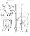
図1は、本発明の第1の実施形態に係る光電変換装置の回路図及びそのタイミングチャートである。
【0026】
本実施形態の光電変換装置は、図に示すように、光電変換手段となるホトダイオード1と、MOSトランジスタ3,3’と、該光電変換手段のリセット手段となるMOSスイッチ2と、
上記光電変換手段のリセット時のノイズ信号を保持するノイズ信号保持手段となるMOSトランジスタ4,6,6’と容量(CM )5と、
同一の上記リセット後に上記光電変換手段が蓄積した信号から上記保持しておいたノイズ信号を用いてノイズを除去するノイズ信号除去手段(7〜16)と、を有することを特徴とする光電変換装置である。
【0027】
また、上記リセット直後のノイズ信号電荷を読み出すノイズ信号読み出し手段としてのMOSスイッチ7,容量(CTN)9と、
光信号蓄積後の光信号電荷を読み出す光信号読み出し手段としてのMOSスイッチ8,容量(CTS)10と、
上記ノイズ信号読み出し手段のノイズ信号と上記光信号読み出し手段の光信号を順次走査する走査手段となるシフトレジスタ13と、
上記走査手段により、上記ノイズ信号読み出し手段(7,9)、及び光信号読み出し手段(8,10)から、信号を読み出すと同時に、上記光電変換手段で光信号蓄積を行なう光電変換装置において、
上記リセット直後のノイズ信号を、前記同一のリセット後蓄積された上記光信号を上記光信号読み出し手段(8,10)に読み出す前まで保持するノイズ信号保持手段(4,5,6,6’)と、
上記保持しておいたリセット直後のノイズ信号と、上記同一のリセット後の上記光信号との差分を出力する手段となるバッファアンプ14,14’,及び差動アンプ15と、
を有することを特徴とする光電変換装置である。
【0028】
ここで、MOSトランジスタ6,6’、及び3,3’は、各々MOSソースフォロアを形成している。
【0029】
また、バッファアンプ14,14’の入力16,16’が共通出力線であり、バッファアンプ14,14’及び差動アンプ15以外は、ビット分有することになる。
【0030】
また、本実施形態においては、図に示す部分を全て、同一半導体基板上に形成している。
【0031】
以下、タイミングチャートを参照しながら、本実施形態の動作及び構成を説明する。
【0032】
まず、スタートパルスSPが入力されると、最初に、光信号、及びノイズ信号蓄積用の容量CTS10及びCTN9がリセットされる。
【0033】
続いて、駆動パルスφTNをONし、容量CM 5に保持されていたノイズ信号を容量CTN9に読み出す。この時、容量CM 5から読み出されるノイズ信号は、前のフィールドにおいて、センサがリセットされた直後のノイズ信号である。容量CTN9にノイズ信号が読み出された後、駆動パルスφT1をONし、光信号を容量CM 5に読み出し、更に駆動パルスφTSをONして容量CTS10に光信号を読み出す。
【0034】
その後、駆動パルスφRをONしてセンサリセットを行ない、続いて駆動パルスφT1をONし、センサリセット直後の信号を、ノイズ信号として容量CM 5に読み出し、センサは、蓄積を開始する。
【0035】
そして、センサが蓄積を行なうのと同時に、容量CTS10、容量CTN9に保持された光信号、及びノイズ信号は、順次、共通出力線に出力され、最終的には、光信号とノイズ信号が、不図示の差分回路等により差分され、正味の光信号として出力されることになる。
【0036】
従って、本発明においては、タイミングチャート中に示す▲1▼のセンサリセットに対するノイズ信号は、蓄積期間中、容量CM 5に保持され(A)、光信号を読み出す前に容量CTN9に入力される(A’)。従って、▲1▼の同一のセンサリセットに対するノイズ信号(A’)と、光信号(B’)の差分を正味の光信号として出力することができるため、センサリセットノイズを完全に除去することが可能となる。
【0037】
また、ノイズ除去手段としては、上述した実施形態に限定されることはなく、例えば、クランプ回路等を用いることも可能である。
【0038】
また、特願61−219666号に開示されているように、差分回路としては、センサ信号を保持する回路と基準信号を保持する回路と、それらの差信号を出力する差動アンプを用いることもできる。
[第2の実施形態]
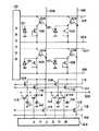
図2は、本発明の第2の実施形態を示す回路図及びタイミングチャートである。
【0039】
本実施形態では、バイポーラトランジスタ1’による光電変換手段を用いた点が、第1の実施形態とは異なる。本実施形態でも、点線で囲った部分がノイズ信号保持手段となり、その構成は第1の実施形態と同じである。
【0040】
以下、タイミングチャートに沿って、動作を説明する。
【0041】
不図示のスタートパルスが入力されると、まず、駆動パルスφCRがONし、光信号蓄積用容量CTS10及びノイズ信号蓄積用容量CTN9がリセットされる。
【0042】
次に、駆動パルスφTNをONしてノイズ信号を容量CTN9に読み出す。
【0043】
次に、駆動パルスφT1をONして光信号を容量CM 5に読み出す。
【0044】
次に、駆動パルスφTSをONして光信号を容量CTS10に読み出す。
【0045】
次に、駆動パルスφBRSをONして、バイポーラトランジスタ1’のベースをVBBにクランプリセットし、更に、駆動パルスφERSをONすることで、センサリセットを行なう。
【0046】
次に、駆動パルスφT1をONして、センサリセット時に発生したノイズ信号を容量CM 5に入力する。その後、センサの蓄積動作を行なう。
【0047】
そして、センサが蓄積を行なうのと同時に、容量CTS10、容量CTN9に保持された光信号、及びノイズ信号は、順次、共通出力線に出力され、最終的には、光信号とノイズ信号が、差分回路15により差分され、正味の光信号として出力されることになる。
【0048】
従って、本発明においても、センサリセットに対するノイズ信号は、蓄積期間中、容量CM 5に保持され、光信号を読み出す前に容量CTN9に入力される。従って、同一のセンサリセットに対するノイズ信号と、光信号の差分を正味の光信号として出力することができるため、センサリセットノイズを完全に除去することが可能となる。
【0049】
なお、ノイズ保持用の容量CM 5は、無くても良く、その場合は、配線や素子の寄生容量を容量CM 5の代わりとして利用することができる。
【0050】
また、本実施形態においては、差動アンプ15以外を、同一半導体基板に形成している。
[第3の実施形態]
図3は、本発明の第3の実施形態に係る光電変換装置の回路図及びそのタイミングチャートである。
【0051】
図において、1はホトダイオードであり、点線で囲った部分は、本発明の特徴となるノイズ信号保持手段であり、ノイズ信号を保持するための容量CM 5と、MOSトランジスタ・スイッチ4、16、17と、MOSトランジスタのソースフォロア回路6,6’とから構成されている。また、光信号蓄積用容量CTS10及びノイズ信号蓄積用容量CTN9を有している。
【0052】
以下、タイミングチャートを参照しながら、本実施形態の動作及び構成を説明する。
【0053】
まず、不図示のスタートパルスSPが入力されると、最初に、駆動パルスφCRがONされて光信号蓄積用の容量CTS10、及びノイズ信号蓄積用の容量CTN9がリセットされる。
【0054】
続いて、駆動パルスφT2をONし、このON期間中に駆動パルスφTNをONし、ノイズ信号を容量CTN9に入力する。
【0055】
次に、駆動パルスφR2をONして、ソースフォロア6,6’をリセットする。
【0056】
次に、駆動パルスφT1をONして、光信号を容量CM 5に入力する。
【0057】
続いて、駆動パルスφT2をONし、このON期間中に駆動パルスφTSをONし、光信号を容量CTS10に入力する。
【0058】
その後、駆動パルスφR1及び駆動パルスφR2をONしてセンサリセット及びソースフォロアリセットを行ない、続いて駆動パルスφT1をONし、センサリセット直後の信号を、ノイズ信号として容量CM 5に読み出し、センサは、蓄積動作を開始する。
【0059】
そして、センサが蓄積を行なうのと同時に、容量CTS10、容量CTN9に保持された光信号、及びノイズ信号は、順次、共通出力線に出力され、最終的には、光信号とノイズ信号が、不図示の差分回路により差分され、正味の光信号として出力されることになる。
【0060】
従って、本発明においても、センサリセットに対するノイズ信号は、蓄積期間中、容量CM 5に保持され、光信号を読み出す前に容量CTN9に入力される。従って、同一のセンサリセットに対するノイズ信号と、光信号の差分を正味の光信号として出力することができるため、センサリセットノイズを完全に除去することが可能となる。
[第4の実施形態]
図4は、本発明の第4の実施形態を示す回路図であり、図5は、そのタイミングチャートである。本実施形態では、前述した本発明の光電変換素子の複数個を2次元状に配列して、水平シフトレジスタH.S.R.及び垂直シフトレジスタV.S.R.を接続した画像読取装置を示すものである。
【0061】
図に示すように、各画素は、光電変換手段としてのホトダイオードと、ノイズ信号保持手段として、MOSトランジスタスイッチ43とソースフォロアとされたMOSトランジスタ44とを持ち、MOSトランジスタ44のゲート容量を前述したノイズ保持用容量として用いている。
【0062】
また、複数個の画素に対して1個ずつの前述した光信号蓄積用容量CTS及びノイズ信号蓄積用容量CTNが接続されている。
【0063】
以下、タイミングチャートを参照しながら、本実施形態の動作及び構成を説明する。
【0064】
まず、不図示のスタートパルスSPが入力されると、最初に、光信号、及びノイズ信号蓄積用の容量CTS及び容量CTNがリセットされる。
【0065】
続いて、駆動パルスφTNをONし、ノイズ信号をMOSトランジスタ44のゲート容量から容量CTNに読み出し、更に駆動パルスφTSをONして容量CTSに光信号を読み出す。
【0066】
その後、駆動パルスφRをONしてセンサリセットを行ない、続いて駆動パルスφT1をONし、センサリセット直後の信号を、MOSトランジスタ42のソースフォロアを介してMOSトランジスタ44のゲート容量に読み出し、センサは、蓄積を開始する。
【0067】
そして、センサが蓄積を行なうのと同時に、容量CTS、容量CTNに保持された光信号、及びノイズ信号は、順次、共通出力線に出力され、最終的には、光信号とノイズ信号が、不図示の差分回路により差分され、正味の光信号として出力されることになる。
【0068】
従って、本発明においては、センサリセットに対するノイズ信号は、蓄積期間中、MOSトランジスタ44のゲート容量に保持され、光信号を読み出す前に容量CTNに入力される。従って、同一のセンサリセットに対するノイズ信号と、光信号の差分を正味の光信号として出力することができるため、センサリセットノイズを完全に除去することが可能となる。
【0069】
また、本実施例のようなエリアセンサ等においては、開口率を向上させる為に、ホトダイオード40として、例えば、アモルファスシリコンのような光導電膜を半導体基板上に積層して用いても良い。
【0070】
【発明の効果】
以上説明したように、本発明によれば、ノイズの保持手段を持ったことにより、1回目のセンサリセット時に発生したノイズを保持した後、そのまま、光信号の蓄積動作と読み出し動作を行ない、1回目のリセットにおけるノイズと光信号の差分をとることができるため、センサリセットノイズの完全な除去ができる。
【0071】
すなわち、本発明においては、センサリセットに対するノイズ信号は、蓄積期間中、ノイズ信号保持手段に保持され、光信号を読み出す前に容量CTNに入力される。従って、センサリセットに対するノイズ信号と、光信号の差分を正味の光信号として出力することができるため、センサリセットノイズを完全に除去することが可能となる。
【図面の簡単な説明】
【図1】本発明の第1の実施形態の回路図及びその動作を示すタイミングチャートである。
【図2】本発明の第2の実施形態の回路図及びその動作を示すタイミングチャートである。
【図3】本発明の第3の実施形態の回路図及びその動作を示すタイミングチャートである。
【図4】本発明の第4実施形態の回路図である。
【図5】本発明の第4実施形態の回路の動作を示すタイミングチャートである。
【図6】従来例1の回路図及びその動作を示すタイミングチャートである。
【図7】従来例2の回路図である。
【図8】従来例2の回路図である。
【符号の説明】
1 光センサ(ホトダイオード)
1’ 光センサ(バイポーラトランジスタ)
2,3,3’,4,6,6’,7,8,11,12 MOSトランジスタ
5 ノイズ信号保持用容量CM
9 ノイズ信号蓄積用容量CTN
10 光信号蓄積用容量CTS
13 シフトレジスタ
14,14’ バッファアンプ
15 差動アンプ
16,16’ 共通出力線
40 ホトダイオード
42,43,44,45,46 MOSトランジスタ
101 ホトダイオード
103 リセットスイッチ
104 画素アンプ
105 垂直ゲート線
106 リセット線
107 ドレイン線
109,110 ゲートスイッチ
111,112 蓄積容量
113,114 水平ゲートスイッチ
116 ゲート線
117 ゲート線
120 水平信号線
122 水平レジスタ[0001]
BACKGROUND OF THE INVENTION
The present invention relates to a photoelectric conversion device, for example, a one-dimensional or two-dimensional photoelectric conversion device that performs reading of a facsimile, a digital copying machine, an X-ray imaging device, or the like, and more particularly, to removal of random noise caused by a reset operation of an optical sensor Is.
[0002]
[Prior art]
Conventionally, CCDs have been mainly used as image reading systems such as facsimiles and digital copying machines, and imaging devices such as video cameras and digital cameras, but in recent years, they have an amplification function for MOS transistors and bipolar transistors in units of pixels. So-called amplification type photoelectric conversion devices are also being actively developed.
[0003]
In order to achieve high sensitivity in an amplification type photoelectric conversion device, it is important to remove noise, but several proposals have been made regarding this noise removal.
[Conventional example 1]
FIG. 6 is a circuit diagram of a one-dimensional photoelectric conversion device having a bipolar transistor as an optical sensor in each pixel, and a timing chart thereof (from Television Society Journal Vol. 47, No. 9 (1993) pp. 1180). .
[0004]
The operation of this photoelectric conversion device will be described below. When the start pulse (SP) is input, the storage capacitors CTS and CTN are reset, and subsequently an optical signal including sensor noise is transferred to CTS .
[0005]
Thereafter, the optical sensor is reset, and the dark output including the sensor noise is transferred toCTN . The sensor is reset again and the accumulation operation starts. At the same time, the shift register of the first chip starts scanning, and the data of CTS and CTN are respectively output to the common output lines CHS and CHN of the first chip by capacity division. The output signals are each input to a differential amplifier via a voltage follower, and a signal without sensor noise is obtained as an output of the IC.
[0006]
Here, a sensor reset noise referred, hFE and bipolar transistors comprising the optical sensor of each pixel refers to the FPN due to the variation in the base / collector capacitance Cbc (Fixed Pattern noise). That is, the emitter potential after emitter reset by φERS varies from pixel to pixel due to variations in hFE and Cbc , and this appears as an offset in normal readout, but this offset can be removed by this method. , FPN can be reduced.
[0007]
[Conventional example 2]
As another conventional example, Japanese Patent Laid-Open No. 1-154678 proposes a solid-state imaging device as shown in FIGS.
[0008]
In the figure, output of signal charges generated by incident light and accumulated in each
[0009]
Next, when the
[0010]
The operation in the horizontal blanking period is as described above, and in the horizontal scanning output period, the
[0011]
The output charge stored in the
[0012]
[Problems to be solved by the invention]
However, in the above-described conventional example, there is a problem to be solved that reset noise generated when the photoelectric conversion means is reset cannot be removed.
[0013]
The reset noise is a fluctuation of the reset potential every time the optical sensor is reset, and appears as random noise.
[0014]
For example, in a photodiode having a pn junction, when the photogenerated carrier QP is accumulated in the capacitor CPD of the photodiode unit and converted into a voltage, the optical signal voltage VP by the photo generated carrier is:
VP = QP / CPD (1)
It becomes. On the other hand, the reset noise VN is
VN = √ (kT / CPD ) (2)
(K: Boltzmann constant, T: temperature (k))
Therefore, the S / N ratio is
VP / VN =QP · √ (1 / (kTCPD )) (3)
[0015]
Therefore, from the equation (3), in order to increase the S / N ratio, it is desirable to make the storage capacitanceCPD of the photosensor as small as possible, but there is a practical limit. On the other hand, high definition of the photoelectric conversion device, with the speed, the signal charge QP is to become the direction of decreasing, eliminating the reset noise, key points of the high S / N of the photoelectric conversion device It becomes.
[0016]
However, in the conventional example 1, as shown in the timing chart of FIG. 6, the sensor reset is performed twice, and the read optical signal and the noise signal are caused by different sensor resets. That is, the accumulation operation and the optical signal readout operation are performed after the second sensor reset, and the sensor noise N generated by the first sensor reset from the readout signal S + N ′ including the sensor noise N ′ generated at the second sensor reset. Since the sensor noise is to be removed by subtracting, random noise that is √2 times the sensor reset noise is generated.
[0017]
In the second prior art, since the
[0018]
Further, in the conventional example 2, an example in which the
[0019]
In other words, although FPN can be improved in the prior art, it has never been improved against random noise caused by the reset operation of the optical sensor.
[0020]
[Object of invention]
An object of the present invention is to reduce random noise caused by a reset operation of a sensor unit in a one-dimensional or two-dimensional photoelectric conversion apparatus that performs optical signal accumulation and signal output simultaneously.
[0021]
[Means for Solving the Problems]
Each of the photoelectric conversion devices of the present invention includes a photoelectric conversion region and an amplification transistor that generates an amplification signal based on a signal obtained by the photoelectric conversion region, and the photoelectric conversion region and the amplification transistor First and second photoelectric conversion means electrically connected tothe input unit, the first photoelectric conversion region and the input unit of the first amplification transistor, and the second photoelectric conversion region and First and second reset means for resetting the input section of the second amplification transistor, respectively, and the first photoelectric conversion means by resetting the first photoelectric conversion means by the first reset means. First signal holding means for temporarily holding a first noise signal generated at the output of the transistor, and resetting the second photoelectric conversion means by the second reset means A second signal holding means for temporarily holding a second noise signal generated at the output of the second amplifying transistor; and a first signal including the first noise signal from the first photoelectric conversion means after storing the optical signal. Before reading out the optical signal to the first signal holding means, the first noise that reads and holds the first noise signal temporarily held in the first signal holding means from the first signal holding means The signal storage capacitor and the second signal holding unit before reading the second optical signal including the second noise signal from the second photoelectric conversion unit to the second signal holding unit after storing the optical signal. A second noise signal storage capacitor for reading out and holding the second noise signal temporarily held in the means from the second signal holding means, and the first photoelectric conversion means from the first photoelectric conversion means after storing the optical signal. Read the signal holding means A first optical signal storage capacitor for reading out and holding the first optical signal that has been output and held from the first signal holding means, and the second signal holding from the second photoelectric conversion means after storing the optical signal The second optical signal read out and held by the means is read out from the second signal holding means and held in the second optical signal storage capacitor and the first and second noise signal storage capacitors, respectively. The first and second optical signals are output via a common noise signal output line, and the first and second optical signals respectively held in the first and second optical signal storage capacitors are Signals output via a common optical signal output line and held in the first noise signal storage capacitor and the first optical signal storage capacitor are the noise signal output line and the optical signal. After each output to the output line, A common output unit for outputting signals held in the second noise signal storage capacitor and the second optical signal storage capacitor to the noise signal output line and the optical signal output line; Noise contained in the first optical signal and the second optical signal output from the common output unit using the first noise signal and the second noise signal output from the output unit Noise removing means for removing each component, and the first and second optical signals from the first and second photoelectric conversion means through the first and second signal holding means, respectively. After reading to the first and second optical signal storage capacitors, the first photoelectric conversion means is reset again by the first reset means, thereby generating a third signal generated at the output of the first amplification transistor. Before the noise signal A fourth noise signal generated at the output of the second amplifying transistor is held in the first signal holding unit, and the second photoelectric conversion unit is reset again by the second reset unit, and the second noise signal is generated in the second signal. The signal is held in the signal holding means .
[0023]
[Action]
According to the present invention, by providing the noise holding means, after the noise generated at the time of sensor reset is held, the accumulation operation and the readout operation of the optical signal are performed as they are, and the difference between the noise and the optical signal at the same sensor reset Therefore, it is possible to completely remove random noise generated when the sensor is reset.
[0024]
DETAILED DESCRIPTION OF THE INVENTION
Hereinafter, embodiments of the present invention will be described in detail with reference to the drawings.
[0025]
[First Embodiment]
FIG. 1 is a circuit diagram and a timing chart of the photoelectric conversion device according to the first embodiment of the present invention.
[0026]
As shown in the figure, the photoelectric conversion device of the present embodiment includes a
Noise signal removing means (7-16) for removing noise from the signal accumulated by the photoelectric conversion means after the same reset using the retained noise signal It is.
[0027]
Also, a
A
A
In the photoelectric conversion apparatus that stores the optical signal by the photoelectric conversion unit at the same time as reading the signal from the noise signal reading unit (7, 9) and the optical signal reading unit (8, 10) by the scanning unit,
Noise signal holding means (4, 5, 6, 6 ′) for holding the noise signal immediately after the reset until the optical signal accumulated after the same reset is read out to the optical signal reading means (8, 10). When,
It is a photoelectric conversion device characterized by having.
[0028]
Here, the
[0029]
Further, the
[0030]
Moreover, in this embodiment, all the parts shown in the figure are formed on the same semiconductor substrate.
[0031]
Hereinafter, the operation and configuration of the present embodiment will be described with reference to a timing chart.
[0032]
First, when the start pulse SP is input, first, the optical signal and noise signal
[0033]
Subsequently, the drive pulse φTN is turned ON, and the noise signal held in the
[0034]
Thereafter, the drive pulse φR is turned on to perform sensor reset, and then the drive pulse φT1 is turned on. The signal immediately after the sensor reset is read as a noise signal to the
[0035]
At the same time as the sensor accumulates, the optical signal and the noise signal held in the
[0036]
Therefore, in the present invention, the noise signal for the sensor reset of (1) shown in the timing chart is held in the
[0037]
Further, the noise removing means is not limited to the above-described embodiment, and for example, a clamp circuit or the like can be used.
[0038]
Further, as disclosed in Japanese Patent Application No. 61-219666, as the difference circuit, a circuit that holds a sensor signal, a circuit that holds a reference signal, and a differential amplifier that outputs the difference signal may be used. it can.
[Second Embodiment]
FIG. 2 is a circuit diagram and a timing chart showing the second embodiment of the present invention.
[0039]
This embodiment is different from the first embodiment in that a photoelectric conversion means using a
[0040]
The operation will be described below along the timing chart.
[0041]
When a start pulse (not shown) is input, first, the drive pulse φCR is turned ON, and the optical signal
[0042]
Next, the drive pulse φTN is turned ON to read the noise signal to the capacitor CTN 9.
[0043]
Next, the drive pulse φT1 is turned on to read the optical signal into the
[0044]
Next, the drive pulse φTS is turned on to read the optical signal to the
[0045]
Then ON the drive pulse FaiBRS, clamp reset the base of the bipolar transistor 1 'to VBB, further, by turning ON the driving pulse FaiERS, perform sensor reset.
[0046]
Next, the drive pulse φT1 is turned ON, and a noise signal generated at the time of sensor reset is input to the
[0047]
At the same time as the sensor accumulates, the optical signal and the noise signal held in the
[0048]
Therefore, also in the present invention, the noise signal for the sensor reset is held in the
[0049]
Note that the noise holding
[0050]
In the present embodiment, components other than the differential amplifier 15 are formed on the same semiconductor substrate.
[Third Embodiment]
FIG. 3 is a circuit diagram and a timing chart of the photoelectric conversion device according to the third embodiment of the present invention.
[0051]
In the figure,
[0052]
Hereinafter, the operation and configuration of the present embodiment will be described with reference to a timing chart.
[0053]
First, when a start pulse SP (not shown) is input, first, the drive pulse φCR is turned on to reset the optical signal
[0054]
Subsequently, the drive pulse φT2 is turned ON, the drive pulse φTN is turned ON during this ON period, and a noise signal is input to the capacitor CTN 9.
[0055]
Next, the drive pulse φR2 is turned on to reset the
[0056]
Next, the drive pulse φT1 is turned ON, and an optical signal is input to the
[0057]
Then, turning ON the driving pulse .phi.T2, turning ON the driving pulse φTS during this ON period, and inputs the optical signal to the
[0058]
Thereafter, the drive pulse φR1 and the drive pulse φR2 are turned on to perform sensor reset and source follower reset, and then the drive pulse φT1 is turned on to read the signal immediately after the sensor reset as a noise signal to the
[0059]
At the same time as the sensor accumulates, the optical signal and the noise signal held in the
[0060]
Therefore, also in the present invention, the noise signal for the sensor reset is held in the
[Fourth Embodiment]
FIG. 4 is a circuit diagram showing a fourth embodiment of the present invention, and FIG. 5 is a timing chart thereof. In this embodiment, a plurality of the photoelectric conversion elements of the present invention described above are arranged in a two-dimensional manner, and the horizontal shift register H.264 is arranged. S. R. And vertical shift register V. S. R. 1 shows an image reading apparatus to which is connected.
[0061]
As shown in the figure, each pixel has a photodiode as a photoelectric conversion means, a MOS transistor switch 43 and a
[0062]
In addition, one optical signal storage capacitorCTS and one noise signal storage capacitorCTN are connected to a plurality of pixels.
[0063]
Hereinafter, the operation and configuration of the present embodiment will be described with reference to a timing chart.
[0064]
First, when a start pulse SP (not shown) is input, first, the optical signal and noise signal storage capacitorCTS and capacitorCTN are reset.
[0065]
Then, turning ON the driving pulse .phi.Tn, read a noise signal from the gate capacitance of the
[0066]
Thereafter, the drive pulse φR is turned on to perform sensor reset, and then the drive pulse φT1 is turned on, and the signal immediately after the sensor reset is read to the gate capacitance of the
[0067]
Simultaneously with the accumulation of the sensor, the optical signal and the noise signal held in the capacitor CTS , the capacitor CTN are sequentially output to the common output line, and finally the optical signal and the noise signal are output. The difference is made by a difference circuit (not shown) and outputted as a net optical signal.
[0068]
Accordingly, in the present invention, the noise signal for the sensor reset, during the accumulation period is held in the gate capacitor of the
[0069]
Further, in the area sensor or the like as in the present embodiment, a photoconductive film such as amorphous silicon may be laminated on the semiconductor substrate as the
[0070]
【The invention's effect】
As described above, according to the present invention, since the noise holding means is provided, after the noise generated at the first sensor reset is held, the optical signal accumulation operation and the readout operation are performed as they are. Since the difference between the noise and the optical signal in the second reset can be taken, the sensor reset noise can be completely removed.
[0071]
That is, in the present invention, the noise signal for the sensor reset, during the accumulation period is held in the noise signal holding means, it is inputted before reading out the optical signal to the capacitor CTN. Therefore, since the difference between the noise signal for the sensor reset and the optical signal can be output as a net optical signal, the sensor reset noise can be completely removed.
[Brief description of the drawings]
FIG. 1 is a circuit diagram of a first embodiment of the present invention and a timing chart showing its operation.
FIG. 2 is a circuit diagram of a second embodiment of the present invention and a timing chart showing its operation.
FIG. 3 is a circuit diagram of a third embodiment of the present invention and a timing chart showing its operation.
FIG. 4 is a circuit diagram of a fourth embodiment of the present invention.
FIG. 5 is a timing chart showing the operation of the circuit of the fourth embodiment of the present invention.
FIG. 6 is a circuit diagram of Conventional Example 1 and a timing chart showing its operation.
FIG. 7 is a circuit diagram of a second conventional example.
FIG. 8 is a circuit diagram of Conventional Example 2.
[Explanation of symbols]
1 Light sensor (photodiode)
1 'Optical sensor (bipolar transistor)
2, 3, 3 ', 4, 6, 6', 7, 8, 11, 12
9 Noise signal storage capacity CTN
10 Optical signal storage capacity CTS
13
Claims (5)
Translated fromJapanese前記第1の光電変換領域及び前記第1の増幅用トランジスタの入力部、そして、前記第2の光電変換領域及び前記第2の増幅用トランジスタの入力部、をそれぞれリセットする第1、第2のリセット手段と、
前記第1のリセット手段により前記第1の光電変換手段をリセットすることにより前記第1の増幅用トランジスタの出力に生じる第1のノイズ信号を一時保持する第1の信号保持手段と、
前記第2のリセット手段により前記第2の光電変換手段をリセットすることにより前記第2の増幅用トランジスタの出力に生じる第2のノイズ信号を一時保持する第2の信号保持手段と、
光信号蓄積後に前記第1の光電変換手段から前記第1のノイズ信号を含む第1の光信号を前記第1の信号保持手段に読み出す前に、前記第1の信号保持手段に一時保持されている前記第1のノイズ信号を前記第1の信号保持手段から読み出し保持する第1のノイズ信号蓄積用容量と、
光信号蓄積後に前記第2の光電変換手段から前記第2のノイズ信号を含む第2の光信号を前記第2の信号保持手段に読み出す前に、前記第2の信号保持手段に一時保持されている前記第2のノイズ信号を前記第2の信号保持手段から読み出し保持する第2のノイズ信号蓄積用容量と、
光信号蓄積後に前記第1の光電変換手段から前記第1の信号保持手段に読み出し保持された前記第1の光信号を前記第1の信号保持手段から読み出し保持する第1の光信号蓄積用容量と、
光信号蓄積後に前記第2の光電変換手段から前記第2の信号保持手段に読み出し保持された前記第2の光信号を前記第2の信号保持手段から読み出し保持する第2の光信号蓄積用容量と、
前記第1及び第2のノイズ信号蓄積用容量にそれぞれ保持された前記第1及び第2のノイズ信号が共通のノイズ信号出力線を介して出力され、
前記第1及び第2の光信号蓄積用容量にそれぞれ保持された前記第1及び第2の光信号が共通の光信号出力線を介して出力され、
且つ、前記第1のノイズ信号蓄積用容量、及び第1の光信号蓄積用容量に保持されている信号が前記ノイズ信号出力線、及び前記光信号出力線にそれぞれ出力された後に、前記第2のノイズ信号蓄積用容量、及び第2の光信号蓄積用容量に保持されている信号が前記ノイズ信号出力線、及び前記光信号出力線にそれぞれ出力される共通出力部と、
前記共通出力部から出力された前記第1のノイズ信号、及び前記第2のノイズ信号を用いて、前記共通出力部から出力された前記第1の光信号、及び前記第2の光信号に含まれるノイズ成分をそれぞれ除去するノイズ除去手段とを有し、
前記第1、第2の光電変換手段から前記第1、第2の光信号を、それぞれ前記第1、第2の信号保持手段を介して前記第1、第2の光信号蓄積用容量にそれぞれ読み出した後、前記第1の光電変換手段を前記第1のリセット手段により再度リセットすることにより前記第1の増幅用トランジスタの出力に生じる第3のノイズ信号を前記第1の信号保持手段に保持し、
前記第2の光電変換手段を前記第2のリセット手段により再度リセットすることにより前記第2の増幅用トランジスタの出力に生じる第4のノイズ信号を前記第2の信号保持手段に保持することを特徴とする光電変換装置。Each includes a photoelectric conversion region and an amplification transistor that generates an amplification signal based on a signal obtained by the photoelectric conversion region, and the photoelectric conversion region and the input portion of the amplification transistor are electrically connected First and second photoelectric conversion means,
First and second resetting the first photoelectric conversion region and the input portion of the first amplification transistor, and the second photoelectric conversion region and the input portion of the second amplification transistor, respectively. Resetting means;
First signal holding means for temporarily holding a first noise signal generated at the output of the first amplification transistor by resetting the first photoelectric conversion means by the first reset means;
Second signal holding means for temporarily holding a second noise signal generated at the output of the second amplification transistor by resetting the second photoelectric conversion means by the second reset means;
Before the first optical signal including the first noise signal is read from the first photoelectric conversion unit to the first signal holding unit after the optical signal is accumulated, the first signal holding unit temporarily holds the first optical signal. A first noise signal storage capacitor for reading and holding the first noise signal from the first signal holding means;
Before the second optical signal including the second noise signal is read from the second photoelectric conversion unit to the second signal holding unit after the optical signal is accumulated, the second signal is temporarily held in the second signal holding unit. A second noise signal storage capacitor for reading and holding the second noise signal from the second signal holding means;
A first optical signal storage capacitor for reading and holding the first optical signal read and held from the first photoelectric conversion means to the first signal holding means after the optical signal is stored. When,
Second optical signal storage capacitor for reading and holding the second optical signal read and held from the second photoelectric conversion means to the second signal holding means after the optical signal is stored. When,
The first and second noise signals respectively held in the first and second noise signal storage capacitors are output via a common noise signal output line,
The first and second optical signals respectively held in the first and second optical signal storage capacitors are output via a common optical signal output line;
In addition, after the signals held in the first noise signal storage capacitor and the first optical signal storage capacitor are output to the noise signal output line and the optical signal output line, respectively, the second A common output unit for outputting a signal held in the noise signal storage capacitor and the second optical signal storage capacitor to the noise signal output line and the optical signal output line, respectively.
Included in the first optical signal and the second optical signal output from the common output unit using the first noise signal and the second noise signal output from the common output unit Noise removing means for removing each noise component generated,
The first and second optical signals from the first and second photoelectric conversion means are respectively sent to the first and second optical signal storage capacitors via the first and second signal holding means, respectively. After reading, the third signal generated at the output of the first amplification transistor is held in the first signal holding means by resetting the first photoelectric conversion means again by the first reset means. And
The second signal holding means holds the fourth noise signal generated at the output of the second amplification transistor by resetting the second photoelectric conversion means again by the second reset means. A photoelectric conversion device.
Priority Applications (5)
| Application Number | Priority Date | Filing Date | Title |
|---|---|---|---|
| JP01033696AJP3774499B2 (en) | 1996-01-24 | 1996-01-24 | Photoelectric conversion device |
| TW086100632ATW359057B (en) | 1996-01-24 | 1997-01-21 | Photoelectric converting apparatus |
| US08/786,183US6538693B1 (en) | 1996-01-24 | 1997-01-21 | Photoelectric conversion apparatus having reset noise holding and removing units |
| KR1019970001941AKR100206099B1 (en) | 1996-01-24 | 1997-01-23 | Photoelectric converter |
| CN97102142ACN1097381C (en) | 1996-01-24 | 1997-01-24 | Photoelectric converting apparatus |
Applications Claiming Priority (1)
| Application Number | Priority Date | Filing Date | Title |
|---|---|---|---|
| JP01033696AJP3774499B2 (en) | 1996-01-24 | 1996-01-24 | Photoelectric conversion device |
Related Child Applications (1)
| Application Number | Title | Priority Date | Filing Date |
|---|---|---|---|
| JP2006008660ADivisionJP4236271B2 (en) | 2006-01-17 | 2006-01-17 | Photoelectric conversion device |
Publications (2)
| Publication Number | Publication Date |
|---|---|
| JPH09205588A JPH09205588A (en) | 1997-08-05 |
| JP3774499B2true JP3774499B2 (en) | 2006-05-17 |
Family
ID=11747364
Family Applications (1)
| Application Number | Title | Priority Date | Filing Date |
|---|---|---|---|
| JP01033696AExpired - Fee RelatedJP3774499B2 (en) | 1996-01-24 | 1996-01-24 | Photoelectric conversion device |
Country Status (5)
| Country | Link |
|---|---|
| US (1) | US6538693B1 (en) |
| JP (1) | JP3774499B2 (en) |
| KR (1) | KR100206099B1 (en) |
| CN (1) | CN1097381C (en) |
| TW (1) | TW359057B (en) |
Families Citing this family (42)
| Publication number | Priority date | Publication date | Assignee | Title |
|---|---|---|---|---|
| JPH11307756A (en) | 1998-02-20 | 1999-11-05 | Canon Inc | Photoelectric conversion device and radiation reader |
| US6963372B1 (en)* | 1998-04-24 | 2005-11-08 | Canon Kabushiki Kaisha | Solid-state image sensing apparatus and method of operating the same |
| JPH11312822A (en)* | 1998-04-28 | 1999-11-09 | Seiko Instruments Inc | Image sensor |
| US6977684B1 (en) | 1998-04-30 | 2005-12-20 | Canon Kabushiki Kaisha | Arrangement of circuits in pixels, each circuit shared by a plurality of pixels, in image sensing apparatus |
| JP3507336B2 (en) | 1998-06-17 | 2004-03-15 | キヤノン株式会社 | Photoelectric conversion device |
| US6850278B1 (en)* | 1998-11-27 | 2005-02-01 | Canon Kabushiki Kaisha | Solid-state image pickup apparatus |
| US6590242B1 (en) | 1999-02-25 | 2003-07-08 | Canon Kabushiki Kaisha | Light-receiving element and photoelectric conversion device |
| US6878977B1 (en) | 1999-02-25 | 2005-04-12 | Canon Kabushiki Kaisha | Photoelectric conversion device, and image sensor and image input system making use of the same |
| JP2000287130A (en)* | 1999-03-31 | 2000-10-13 | Sharp Corp | Amplification type solid-state imaging device |
| JP3466953B2 (en) | 1999-04-12 | 2003-11-17 | キヤノン株式会社 | Image sensor |
| JP2000324406A (en) | 1999-05-07 | 2000-11-24 | Canon Inc | Photoelectric conversion device and image reading system using the same |
| JP2001024949A (en)* | 1999-07-08 | 2001-01-26 | Canon Inc | Solid-state imaging device and imaging system using the same |
| JP4119052B2 (en)* | 1999-07-16 | 2008-07-16 | 浜松ホトニクス株式会社 | Photodetector |
| JP3524440B2 (en)* | 1999-07-27 | 2004-05-10 | キヤノン株式会社 | Solid-state imaging device and driving method thereof |
| JP2001086414A (en)* | 1999-09-10 | 2001-03-30 | Sony Corp | Imaging device and signal processing method |
| AU2001293062A1 (en)* | 2000-09-25 | 2002-04-08 | Foveon, Inc. | Active pixel sensor with noise cancellation |
| US6950131B1 (en)* | 2000-09-26 | 2005-09-27 | Valley Oak Semiconductor | Simultaneous access and reset system for an active pixel sensor |
| US20020097446A1 (en)* | 2001-01-25 | 2002-07-25 | Umax Data Systems Inc. | Apparatus and method for dark calibration of a linear CMOS sensor |
| FR2819941B1 (en)* | 2001-01-25 | 2003-06-20 | Get Int | PHOTOELECTRIC ELEMENT WITH VERY HIGH OPERATING DYNAMICS |
| JP4809999B2 (en)* | 2001-05-25 | 2011-11-09 | キヤノン株式会社 | Radiation imaging apparatus and radiation imaging system |
| JP2003007995A (en)* | 2001-06-20 | 2003-01-10 | Iwate Toshiba Electronics Co Ltd | CMOS image sensor |
| TW200511843A (en) | 2003-08-29 | 2005-03-16 | Rohm Co Ltd | Photo-electric conversion device |
| JP2005130322A (en)* | 2003-10-27 | 2005-05-19 | Matsushita Electric Ind Co Ltd | Image sensor noise removal device |
| US7446806B2 (en)* | 2003-12-19 | 2008-11-04 | Symbol Technologies, Inc. | Single chip, noise-resistant, one-dimensional, CMOS sensor for target imaging |
| JP4412547B2 (en)* | 2005-02-28 | 2010-02-10 | セイコーインスツル株式会社 | Photoelectric conversion device and image sensor |
| JP4771535B2 (en)* | 2005-05-17 | 2011-09-14 | キヤノン株式会社 | Imaging apparatus and control method |
| JP4486015B2 (en)* | 2005-09-13 | 2010-06-23 | パナソニック株式会社 | Solid-state imaging device |
| JP5012188B2 (en)* | 2007-05-14 | 2012-08-29 | コニカミノルタホールディングス株式会社 | Solid-state imaging device |
| JP4673396B2 (en)* | 2007-09-14 | 2011-04-20 | キヤノン株式会社 | Imaging apparatus and imaging system |
| EP2037667B1 (en)* | 2007-09-14 | 2017-08-23 | Canon Kabushiki Kaisha | Image sensing apparatus and imaging system |
| JP4509202B2 (en)* | 2008-06-09 | 2010-07-21 | キヤノン株式会社 | Signal processing apparatus and imaging apparatus |
| JP5222068B2 (en)* | 2008-09-08 | 2013-06-26 | キヤノン株式会社 | Imaging device |
| JP5355026B2 (en)* | 2008-10-09 | 2013-11-27 | キヤノン株式会社 | Imaging device |
| KR101696410B1 (en)* | 2009-11-11 | 2017-01-16 | 삼성전자주식회사 | Image sensor and method of operating the same |
| JP2013153857A (en)* | 2012-01-27 | 2013-08-15 | Canon Inc | Radiation imaging system and control method of the same |
| JP6586793B2 (en)* | 2015-06-30 | 2019-10-09 | 株式会社リコー | Photoelectric conversion device and image generation device |
| WO2017022451A1 (en)* | 2015-07-31 | 2017-02-09 | ソニーセミコンダクタソリューションズ株式会社 | Solid-state imaging device and electronic device |
| US9819883B2 (en)* | 2015-12-03 | 2017-11-14 | Omnivision Technologies, Inc. | Global shutter correction |
| JP6688451B2 (en)* | 2016-02-29 | 2020-04-28 | 株式会社リコー | Solid-state imaging device and image reading device |
| JP6960831B2 (en) | 2017-11-17 | 2021-11-05 | エイブリック株式会社 | Sensor device |
| JP6998741B2 (en) | 2017-11-20 | 2022-01-18 | エイブリック株式会社 | Sensor device |
| KR20240107546A (en) | 2022-12-30 | 2024-07-09 | 동의대학교 산학협력단 | Anti-tangle comb |
Family Cites Families (63)
| Publication number | Priority date | Publication date | Assignee | Title |
|---|---|---|---|---|
| USB299480I5 (en) | 1972-10-20 | |||
| US3904818A (en) | 1974-02-28 | 1975-09-09 | Rca Corp | Removal of dark current spikes from image sensor output signals |
| FR2356328A1 (en) | 1976-06-24 | 1978-01-20 | Ibm France | NOISE ELIMINATION DEVICE IN SELF-SCANNING PHOTOSENSITIVE NETWORKS |
| JPS5378112A (en) | 1976-12-22 | 1978-07-11 | Toshiba Corp | Charge transfer type pick up unit |
| JPS54130828A (en) | 1978-03-31 | 1979-10-11 | Canon Inc | Photo sensor array device and image scanner using it |
| JPS5822900B2 (en) | 1978-09-25 | 1983-05-12 | 株式会社日立製作所 | solid-state imaging device |
| JPS5568879A (en) | 1978-11-16 | 1980-05-23 | Hitachi Ltd | Chopper device |
| JPS5578680A (en) | 1978-12-08 | 1980-06-13 | Matsushita Electric Ind Co Ltd | Solid state pickup device |
| JPS55104174A (en) | 1979-02-05 | 1980-08-09 | Nec Corp | Solidstate pick up unit |
| US4216503A (en) | 1979-03-26 | 1980-08-05 | Xerox Corporation | Signal restoration and gain control for image viewing devices |
| DE2936703A1 (en) | 1979-09-11 | 1981-03-26 | Siemens AG, 1000 Berlin und 8000 München | MONOLITHICALLY INTEGRATED CIRCUIT WITH A TWO-DIMENSIONAL IMAGE SENSOR |
| DE2939490A1 (en) | 1979-09-28 | 1981-04-16 | Siemens AG, 1000 Berlin und 8000 München | MONOLITHICALLY INTEGRATED TWO-DIMENSIONAL IMAGE SENSOR WITH A DIFFERENTIAL LEVEL |
| JPS56116374A (en) | 1980-02-20 | 1981-09-12 | Sony Corp | Charge detection circuit |
| JPS5741081A (en) | 1980-08-23 | 1982-03-06 | Shoichi Tanaka | Solid image pickup device |
| US4392157A (en) | 1980-10-31 | 1983-07-05 | Eastman Kodak Company | Pattern noise reduction method and apparatus for solid state image sensors |
| DE3049130A1 (en) | 1980-12-24 | 1982-07-15 | Robert Bosch Gmbh, 7000 Stuttgart | Read circuit for solid-state imaging array - eliminates noise by reading each line twice and then subtracting |
| JPS57140073A (en) | 1981-02-20 | 1982-08-30 | Fujitsu Ltd | Solid-state image pickup device |
| JPS57184376A (en) | 1981-05-09 | 1982-11-13 | Sony Corp | Signal output circuit of image pickup device |
| JPS5813079A (en) | 1981-07-16 | 1983-01-25 | Olympus Optical Co Ltd | Image sensor |
| JPS5870687A (en) | 1981-10-22 | 1983-04-27 | Matsushita Electric Ind Co Ltd | Driving method of solid-state image sensor |
| JPS5884568A (en) | 1981-11-13 | 1983-05-20 | Fuji Xerox Co Ltd | Original reading device |
| FR2517864A1 (en) | 1981-12-07 | 1983-06-10 | Telecommunications Sa | DEVICE FOR RECORDING AND READING IMAGES |
| JPS58111579A (en) | 1981-12-25 | 1983-07-02 | Hitachi Ltd | solid-state imaging device |
| JPS5915167A (en) | 1982-07-13 | 1984-01-26 | 丸五株式会社 | Assembling of reinforcing cage for concrete pillar |
| JPS5923765A (en) | 1982-07-30 | 1984-02-07 | 株式会社日立製作所 | vehicle seat |
| JPS5986379A (en) | 1982-11-08 | 1984-05-18 | Toshiba Corp | Photoelectric conversion device |
| JPS59108476A (en) | 1982-12-14 | 1984-06-22 | Junichi Nishizawa | Two-dimensional solid-state image pickup device and its readout method |
| JPS59144169A (en) | 1983-02-07 | 1984-08-18 | Hitachi Ltd | solid-state image sensor |
| JPS6012760A (en) | 1983-07-02 | 1985-01-23 | Tadahiro Omi | Photoelectric conversion device and photoelectric conversion method |
| JPS6012765A (en) | 1983-07-02 | 1985-01-23 | Tadahiro Omi | Photoelectric conversion device |
| JPS6012759A (en) | 1983-07-02 | 1985-01-23 | Tadahiro Omi | Photoelectric conversion device |
| JPS6012763A (en) | 1983-07-02 | 1985-01-23 | Tadahiro Omi | Photoelectric conversion device |
| US4686554A (en) | 1983-07-02 | 1987-08-11 | Canon Kabushiki Kaisha | Photoelectric converter |
| JPS6012761A (en) | 1983-07-02 | 1985-01-23 | Tadahiro Omi | Photoelectric conversion device |
| JPS6012762A (en) | 1983-07-02 | 1985-01-23 | Tadahiro Omi | Photoelectric conversion device |
| JPS6012764A (en) | 1983-07-02 | 1985-01-23 | Tadahiro Omi | Photoelectric conversion device |
| US4742392A (en) | 1983-08-04 | 1988-05-03 | Canon Kabushiki Kaisha | Clamp circuit with feed back |
| JPS6058780A (en) | 1983-09-09 | 1985-04-04 | Olympus Optical Co Ltd | Solid-state image pickup device provided with photometric function |
| JPS6058781A (en) | 1983-09-09 | 1985-04-04 | Olympus Optical Co Ltd | solid-state imaging device |
| JPS60100886A (en) | 1983-11-05 | 1985-06-04 | Junichi Nishizawa | Two-dimensional solid-state pickup device and its signal detection method |
| JPH0831991B2 (en) | 1984-04-17 | 1996-03-27 | オリンパス光学工業株式会社 | Solid-state imaging device |
| JPS6181087A (en) | 1984-09-28 | 1986-04-24 | Olympus Optical Co Ltd | solid-state imaging device |
| EP0455311B1 (en) | 1984-12-26 | 2001-03-14 | Canon Kabushiki Kaisha | Image sensor device |
| CA1269446A (en) | 1984-12-28 | 1990-05-22 | Seiji Hashimoto | Image sensing apparatus |
| JPS61219666A (en) | 1985-03-26 | 1986-09-30 | Toshiba Corp | Thermal head |
| CA1289242C (en) | 1985-11-13 | 1991-09-17 | Shigetoshi Sugawa | Device and method of photoelectrically converting light into electrical signal |
| US5737016A (en) | 1985-11-15 | 1998-04-07 | Canon Kabushiki Kaisha | Solid state image pickup apparatus for reducing noise |
| US5771070A (en) | 1985-11-15 | 1998-06-23 | Canon Kabushiki Kaisha | Solid state image pickup apparatus removing noise from the photoelectric converted signal |
| US4914519A (en)* | 1986-09-19 | 1990-04-03 | Canon Kabushiki Kaisha | Apparatus for eliminating noise in a solid-state image pickup device |
| JPH084127B2 (en) | 1986-09-30 | 1996-01-17 | キヤノン株式会社 | Photoelectric conversion device |
| JPH0824352B2 (en) | 1986-02-10 | 1996-03-06 | 株式会社日立製作所 | Solid-state imaging device |
| US4644287A (en)* | 1986-03-10 | 1987-02-17 | Rca Corporation | Low noise synchronous detection for a charge transfer device |
| JPH01154678A (en) | 1987-12-11 | 1989-06-16 | Hitachi Ltd | solid state imaging device |
| US5019602A (en) | 1989-12-12 | 1991-05-28 | Premier Industrial Corporation | Polyurethane foams, compositions to prepare same and process to prepare same |
| US5276521A (en)* | 1990-07-30 | 1994-01-04 | Olympus Optical Co., Ltd. | Solid state imaging device having a constant pixel integrating period and blooming resistance |
| JP2965777B2 (en)* | 1992-01-29 | 1999-10-18 | オリンパス光学工業株式会社 | Solid-state imaging device |
| US5949483A (en)* | 1994-01-28 | 1999-09-07 | California Institute Of Technology | Active pixel sensor array with multiresolution readout |
| US5841126A (en)* | 1994-01-28 | 1998-11-24 | California Institute Of Technology | CMOS active pixel sensor type imaging system on a chip |
| US5471515A (en)* | 1994-01-28 | 1995-11-28 | California Institute Of Technology | Active pixel sensor with intra-pixel charge transfer |
| US5473660A (en)* | 1994-06-01 | 1995-12-05 | U.S. Philips Corporation | Image sensing device |
| US5631704A (en)* | 1994-10-14 | 1997-05-20 | Lucent Technologies, Inc. | Active pixel sensor and imaging system having differential mode |
| US5576763A (en)* | 1994-11-22 | 1996-11-19 | Lucent Technologies Inc. | Single-polysilicon CMOS active pixel |
| US5608243A (en)* | 1995-10-19 | 1997-03-04 | National Semiconductor Corporation | Single split-gate MOS transistor active pixel sensor cell with automatic anti-blooming and wide dynamic range |
- 1996
- 1996-01-24JPJP01033696Apatent/JP3774499B2/ennot_activeExpired - Fee Related
- 1997
- 1997-01-21TWTW086100632Apatent/TW359057B/ennot_activeIP Right Cessation
- 1997-01-21USUS08/786,183patent/US6538693B1/ennot_activeExpired - Lifetime
- 1997-01-23KRKR1019970001941Apatent/KR100206099B1/ennot_activeExpired - Fee Related
- 1997-01-24CNCN97102142Apatent/CN1097381C/ennot_activeExpired - Fee Related
Also Published As
| Publication number | Publication date |
|---|---|
| TW359057B (en) | 1999-05-21 |
| KR970059850A (en) | 1997-08-12 |
| CN1097381C (en) | 2002-12-25 |
| JPH09205588A (en) | 1997-08-05 |
| US6538693B1 (en) | 2003-03-25 |
| KR100206099B1 (en) | 1999-07-01 |
| CN1162888A (en) | 1997-10-22 |
Similar Documents
| Publication | Publication Date | Title |
|---|---|---|
| JP3774499B2 (en) | Photoelectric conversion device | |
| US8698935B2 (en) | Solid-state image pickup device and camera having arrayed pixels including amplifying units | |
| JP5821315B2 (en) | Electronic device, driving method of electronic device | |
| US9343500B2 (en) | Solid-state imaging device, driving method thereof, and electronic device | |
| US8513710B2 (en) | Solid-state imaging device and control method for same | |
| EP0793378B1 (en) | Photoelectric conversion device using charge skimming | |
| US9001243B2 (en) | Imaging apparatus and processing method thereof | |
| KR101945052B1 (en) | Solid-state imaging device, method of driving the same, and electronic system | |
| JP3507336B2 (en) | Photoelectric conversion device | |
| JPH11122532A (en) | Solid-state imaging device and driving method thereof | |
| KR20000048439A (en) | Photodiode active pixel sensor with shared reset signal row select | |
| KR20180113506A (en) | Solid-state imaging device, method of driving solid-state imaging device, and electronic device | |
| US9794497B2 (en) | Solid-state imaging device controlling read-out of signals from pixels in first and second areas | |
| JP2708455B2 (en) | Solid-state imaging device | |
| JP3890207B2 (en) | Imaging apparatus and imaging system | |
| JP2001238132A (en) | Mos-type solid-state imaging apparatus and image pickup method therefor | |
| JP2003017677A (en) | Imaging device | |
| JP4236271B2 (en) | Photoelectric conversion device | |
| JP2005051282A (en) | Driving device and imaging device | |
| JP2000295530A (en) | Solid-state imaging device | |
| JP2014078869A (en) | Solid-state imaging element, imaging apparatus and drive control method of solid-state imaging element | |
| JP4746962B2 (en) | Solid-state imaging device and imaging system | |
| JPH1093868A (en) | Solid-state image pickup element and its drive method | |
| JP3149126B2 (en) | Solid-state imaging device | |
| JP3037993B2 (en) | Solid-state imaging device |
Legal Events
| Date | Code | Title | Description |
|---|---|---|---|
| A521 | Request for written amendment filed | Free format text:JAPANESE INTERMEDIATE CODE: A523 Effective date:20031217 | |
| A911 | Transfer to examiner for re-examination before appeal (zenchi) | Free format text:JAPANESE INTERMEDIATE CODE: A911 Effective date:20031222 | |
| A912 | Re-examination (zenchi) completed and case transferred to appeal board | Free format text:JAPANESE INTERMEDIATE CODE: A912 Effective date:20040220 | |
| A521 | Request for written amendment filed | Free format text:JAPANESE INTERMEDIATE CODE: A523 Effective date:20060117 | |
| A61 | First payment of annual fees (during grant procedure) | Free format text:JAPANESE INTERMEDIATE CODE: A61 Effective date:20060220 | |
| R150 | Certificate of patent or registration of utility model | Free format text:JAPANESE INTERMEDIATE CODE: R150 | |
| FPAY | Renewal fee payment (event date is renewal date of database) | Free format text:PAYMENT UNTIL: 20100224 Year of fee payment:4 | |
| FPAY | Renewal fee payment (event date is renewal date of database) | Free format text:PAYMENT UNTIL: 20100224 Year of fee payment:4 | |
| FPAY | Renewal fee payment (event date is renewal date of database) | Free format text:PAYMENT UNTIL: 20110224 Year of fee payment:5 | |
| FPAY | Renewal fee payment (event date is renewal date of database) | Free format text:PAYMENT UNTIL: 20120224 Year of fee payment:6 | |
| FPAY | Renewal fee payment (event date is renewal date of database) | Free format text:PAYMENT UNTIL: 20130224 Year of fee payment:7 | |
| FPAY | Renewal fee payment (event date is renewal date of database) | Free format text:PAYMENT UNTIL: 20140224 Year of fee payment:8 | |
| LAPS | Cancellation because of no payment of annual fees |