JP3772066B2 - Semiconductor device - Google Patents
Semiconductor deviceDownload PDFInfo
- Publication number
- JP3772066B2 JP3772066B2JP2000071027AJP2000071027AJP3772066B2JP 3772066 B2JP3772066 B2JP 3772066B2JP 2000071027 AJP2000071027 AJP 2000071027AJP 2000071027 AJP2000071027 AJP 2000071027AJP 3772066 B2JP3772066 B2JP 3772066B2
- Authority
- JP
- Japan
- Prior art keywords
- chip
- package
- conductor
- pad
- chips
- Prior art date
- Legal status (The legal status is an assumption and is not a legal conclusion. Google has not performed a legal analysis and makes no representation as to the accuracy of the status listed.)
- Expired - Fee Related
Links
Images


Classifications
- H—ELECTRICITY
- H01—ELECTRIC ELEMENTS
- H01L—SEMICONDUCTOR DEVICES NOT COVERED BY CLASS H10
- H01L23/00—Details of semiconductor or other solid state devices
- H01L23/28—Encapsulations, e.g. encapsulating layers, coatings, e.g. for protection
- H01L23/31—Encapsulations, e.g. encapsulating layers, coatings, e.g. for protection characterised by the arrangement or shape
- H01L23/3107—Encapsulations, e.g. encapsulating layers, coatings, e.g. for protection characterised by the arrangement or shape the device being completely enclosed
- H—ELECTRICITY
- H01—ELECTRIC ELEMENTS
- H01L—SEMICONDUCTOR DEVICES NOT COVERED BY CLASS H10
- H01L24/00—Arrangements for connecting or disconnecting semiconductor or solid-state bodies; Methods or apparatus related thereto
- H01L24/01—Means for bonding being attached to, or being formed on, the surface to be connected, e.g. chip-to-package, die-attach, "first-level" interconnects; Manufacturing methods related thereto
- H01L24/18—High density interconnect [HDI] connectors; Manufacturing methods related thereto
- H01L24/23—Structure, shape, material or disposition of the high density interconnect connectors after the connecting process
- H01L24/24—Structure, shape, material or disposition of the high density interconnect connectors after the connecting process of an individual high density interconnect connector
- H—ELECTRICITY
- H01—ELECTRIC ELEMENTS
- H01L—SEMICONDUCTOR DEVICES NOT COVERED BY CLASS H10
- H01L24/00—Arrangements for connecting or disconnecting semiconductor or solid-state bodies; Methods or apparatus related thereto
- H01L24/93—Batch processes
- H01L24/94—Batch processes at wafer-level, i.e. with connecting carried out on a wafer comprising a plurality of undiced individual devices
- H—ELECTRICITY
- H01—ELECTRIC ELEMENTS
- H01L—SEMICONDUCTOR DEVICES NOT COVERED BY CLASS H10
- H01L24/00—Arrangements for connecting or disconnecting semiconductor or solid-state bodies; Methods or apparatus related thereto
- H01L24/93—Batch processes
- H01L24/95—Batch processes at chip-level, i.e. with connecting carried out on a plurality of singulated devices, i.e. on diced chips
- H01L24/97—Batch processes at chip-level, i.e. with connecting carried out on a plurality of singulated devices, i.e. on diced chips the devices being connected to a common substrate, e.g. interposer, said common substrate being separable into individual assemblies after connecting
- H—ELECTRICITY
- H01—ELECTRIC ELEMENTS
- H01L—SEMICONDUCTOR DEVICES NOT COVERED BY CLASS H10
- H01L25/00—Assemblies consisting of a plurality of semiconductor or other solid state devices
- H01L25/03—Assemblies consisting of a plurality of semiconductor or other solid state devices all the devices being of a type provided for in a single subclass of subclasses H10B, H10D, H10F, H10H, H10K or H10N, e.g. assemblies of rectifier diodes
- H01L25/04—Assemblies consisting of a plurality of semiconductor or other solid state devices all the devices being of a type provided for in a single subclass of subclasses H10B, H10D, H10F, H10H, H10K or H10N, e.g. assemblies of rectifier diodes the devices not having separate containers
- H01L25/065—Assemblies consisting of a plurality of semiconductor or other solid state devices all the devices being of a type provided for in a single subclass of subclasses H10B, H10D, H10F, H10H, H10K or H10N, e.g. assemblies of rectifier diodes the devices not having separate containers the devices being of a type provided for in group H10D89/00
- H01L25/0652—Assemblies consisting of a plurality of semiconductor or other solid state devices all the devices being of a type provided for in a single subclass of subclasses H10B, H10D, H10F, H10H, H10K or H10N, e.g. assemblies of rectifier diodes the devices not having separate containers the devices being of a type provided for in group H10D89/00 the devices being arranged next and on each other, i.e. mixed assemblies
- H—ELECTRICITY
- H01—ELECTRIC ELEMENTS
- H01L—SEMICONDUCTOR DEVICES NOT COVERED BY CLASS H10
- H01L25/00—Assemblies consisting of a plurality of semiconductor or other solid state devices
- H01L25/03—Assemblies consisting of a plurality of semiconductor or other solid state devices all the devices being of a type provided for in a single subclass of subclasses H10B, H10D, H10F, H10H, H10K or H10N, e.g. assemblies of rectifier diodes
- H01L25/04—Assemblies consisting of a plurality of semiconductor or other solid state devices all the devices being of a type provided for in a single subclass of subclasses H10B, H10D, H10F, H10H, H10K or H10N, e.g. assemblies of rectifier diodes the devices not having separate containers
- H01L25/065—Assemblies consisting of a plurality of semiconductor or other solid state devices all the devices being of a type provided for in a single subclass of subclasses H10B, H10D, H10F, H10H, H10K or H10N, e.g. assemblies of rectifier diodes the devices not having separate containers the devices being of a type provided for in group H10D89/00
- H01L25/0657—Stacked arrangements of devices
- H—ELECTRICITY
- H01—ELECTRIC ELEMENTS
- H01L—SEMICONDUCTOR DEVICES NOT COVERED BY CLASS H10
- H01L2224/00—Indexing scheme for arrangements for connecting or disconnecting semiconductor or solid-state bodies and methods related thereto as covered by H01L24/00
- H01L2224/01—Means for bonding being attached to, or being formed on, the surface to be connected, e.g. chip-to-package, die-attach, "first-level" interconnects; Manufacturing methods related thereto
- H01L2224/02—Bonding areas; Manufacturing methods related thereto
- H01L2224/04—Structure, shape, material or disposition of the bonding areas prior to the connecting process
- H01L2224/0401—Bonding areas specifically adapted for bump connectors, e.g. under bump metallisation [UBM]
- H—ELECTRICITY
- H01—ELECTRIC ELEMENTS
- H01L—SEMICONDUCTOR DEVICES NOT COVERED BY CLASS H10
- H01L2224/00—Indexing scheme for arrangements for connecting or disconnecting semiconductor or solid-state bodies and methods related thereto as covered by H01L24/00
- H01L2224/01—Means for bonding being attached to, or being formed on, the surface to be connected, e.g. chip-to-package, die-attach, "first-level" interconnects; Manufacturing methods related thereto
- H01L2224/02—Bonding areas; Manufacturing methods related thereto
- H01L2224/04—Structure, shape, material or disposition of the bonding areas prior to the connecting process
- H01L2224/04105—Bonding areas formed on an encapsulation of the semiconductor or solid-state body, e.g. bonding areas on chip-scale packages
- H—ELECTRICITY
- H01—ELECTRIC ELEMENTS
- H01L—SEMICONDUCTOR DEVICES NOT COVERED BY CLASS H10
- H01L2224/00—Indexing scheme for arrangements for connecting or disconnecting semiconductor or solid-state bodies and methods related thereto as covered by H01L24/00
- H01L2224/01—Means for bonding being attached to, or being formed on, the surface to be connected, e.g. chip-to-package, die-attach, "first-level" interconnects; Manufacturing methods related thereto
- H01L2224/10—Bump connectors; Manufacturing methods related thereto
- H01L2224/12—Structure, shape, material or disposition of the bump connectors prior to the connecting process
- H01L2224/12105—Bump connectors formed on an encapsulation of the semiconductor or solid-state body, e.g. bumps on chip-scale packages
- H—ELECTRICITY
- H01—ELECTRIC ELEMENTS
- H01L—SEMICONDUCTOR DEVICES NOT COVERED BY CLASS H10
- H01L2224/00—Indexing scheme for arrangements for connecting or disconnecting semiconductor or solid-state bodies and methods related thereto as covered by H01L24/00
- H01L2224/01—Means for bonding being attached to, or being formed on, the surface to be connected, e.g. chip-to-package, die-attach, "first-level" interconnects; Manufacturing methods related thereto
- H01L2224/10—Bump connectors; Manufacturing methods related thereto
- H01L2224/12—Structure, shape, material or disposition of the bump connectors prior to the connecting process
- H01L2224/14—Structure, shape, material or disposition of the bump connectors prior to the connecting process of a plurality of bump connectors
- H01L2224/141—Disposition
- H01L2224/1418—Disposition being disposed on at least two different sides of the body, e.g. dual array
- H01L2224/14181—On opposite sides of the body
- H—ELECTRICITY
- H01—ELECTRIC ELEMENTS
- H01L—SEMICONDUCTOR DEVICES NOT COVERED BY CLASS H10
- H01L2224/00—Indexing scheme for arrangements for connecting or disconnecting semiconductor or solid-state bodies and methods related thereto as covered by H01L24/00
- H01L2224/01—Means for bonding being attached to, or being formed on, the surface to be connected, e.g. chip-to-package, die-attach, "first-level" interconnects; Manufacturing methods related thereto
- H01L2224/10—Bump connectors; Manufacturing methods related thereto
- H01L2224/15—Structure, shape, material or disposition of the bump connectors after the connecting process
- H01L2224/16—Structure, shape, material or disposition of the bump connectors after the connecting process of an individual bump connector
- H01L2224/161—Disposition
- H01L2224/16135—Disposition the bump connector connecting between different semiconductor or solid-state bodies, i.e. chip-to-chip
- H01L2224/16145—Disposition the bump connector connecting between different semiconductor or solid-state bodies, i.e. chip-to-chip the bodies being stacked
- H—ELECTRICITY
- H01—ELECTRIC ELEMENTS
- H01L—SEMICONDUCTOR DEVICES NOT COVERED BY CLASS H10
- H01L2224/00—Indexing scheme for arrangements for connecting or disconnecting semiconductor or solid-state bodies and methods related thereto as covered by H01L24/00
- H01L2224/01—Means for bonding being attached to, or being formed on, the surface to be connected, e.g. chip-to-package, die-attach, "first-level" interconnects; Manufacturing methods related thereto
- H01L2224/18—High density interconnect [HDI] connectors; Manufacturing methods related thereto
- H01L2224/23—Structure, shape, material or disposition of the high density interconnect connectors after the connecting process
- H01L2224/24—Structure, shape, material or disposition of the high density interconnect connectors after the connecting process of an individual high density interconnect connector
- H01L2224/241—Disposition
- H01L2224/24135—Connecting between different semiconductor or solid-state bodies, i.e. chip-to-chip
- H01L2224/24145—Connecting between different semiconductor or solid-state bodies, i.e. chip-to-chip the bodies being stacked
- H01L2224/24146—Connecting between different semiconductor or solid-state bodies, i.e. chip-to-chip the bodies being stacked the HDI interconnect connecting to the same level of the lower semiconductor or solid-state body at which the upper semiconductor or solid-state body is mounted
- H—ELECTRICITY
- H01—ELECTRIC ELEMENTS
- H01L—SEMICONDUCTOR DEVICES NOT COVERED BY CLASS H10
- H01L2224/00—Indexing scheme for arrangements for connecting or disconnecting semiconductor or solid-state bodies and methods related thereto as covered by H01L24/00
- H01L2224/01—Means for bonding being attached to, or being formed on, the surface to be connected, e.g. chip-to-package, die-attach, "first-level" interconnects; Manufacturing methods related thereto
- H01L2224/26—Layer connectors, e.g. plate connectors, solder or adhesive layers; Manufacturing methods related thereto
- H01L2224/27—Manufacturing methods
- H01L2224/274—Manufacturing methods by blanket deposition of the material of the layer connector
- H—ELECTRICITY
- H01—ELECTRIC ELEMENTS
- H01L—SEMICONDUCTOR DEVICES NOT COVERED BY CLASS H10
- H01L2224/00—Indexing scheme for arrangements for connecting or disconnecting semiconductor or solid-state bodies and methods related thereto as covered by H01L24/00
- H01L2224/01—Means for bonding being attached to, or being formed on, the surface to be connected, e.g. chip-to-package, die-attach, "first-level" interconnects; Manufacturing methods related thereto
- H01L2224/26—Layer connectors, e.g. plate connectors, solder or adhesive layers; Manufacturing methods related thereto
- H01L2224/31—Structure, shape, material or disposition of the layer connectors after the connecting process
- H01L2224/32—Structure, shape, material or disposition of the layer connectors after the connecting process of an individual layer connector
- H01L2224/321—Disposition
- H01L2224/32135—Disposition the layer connector connecting between different semiconductor or solid-state bodies, i.e. chip-to-chip
- H01L2224/32145—Disposition the layer connector connecting between different semiconductor or solid-state bodies, i.e. chip-to-chip the bodies being stacked
- H—ELECTRICITY
- H01—ELECTRIC ELEMENTS
- H01L—SEMICONDUCTOR DEVICES NOT COVERED BY CLASS H10
- H01L2224/00—Indexing scheme for arrangements for connecting or disconnecting semiconductor or solid-state bodies and methods related thereto as covered by H01L24/00
- H01L2224/01—Means for bonding being attached to, or being formed on, the surface to be connected, e.g. chip-to-package, die-attach, "first-level" interconnects; Manufacturing methods related thereto
- H01L2224/26—Layer connectors, e.g. plate connectors, solder or adhesive layers; Manufacturing methods related thereto
- H01L2224/31—Structure, shape, material or disposition of the layer connectors after the connecting process
- H01L2224/32—Structure, shape, material or disposition of the layer connectors after the connecting process of an individual layer connector
- H01L2224/321—Disposition
- H01L2224/32151—Disposition the layer connector connecting between a semiconductor or solid-state body and an item not being a semiconductor or solid-state body, e.g. chip-to-substrate, chip-to-passive
- H01L2224/32221—Disposition the layer connector connecting between a semiconductor or solid-state body and an item not being a semiconductor or solid-state body, e.g. chip-to-substrate, chip-to-passive the body and the item being stacked
- H01L2224/32225—Disposition the layer connector connecting between a semiconductor or solid-state body and an item not being a semiconductor or solid-state body, e.g. chip-to-substrate, chip-to-passive the body and the item being stacked the item being non-metallic, e.g. insulating substrate with or without metallisation
- H—ELECTRICITY
- H01—ELECTRIC ELEMENTS
- H01L—SEMICONDUCTOR DEVICES NOT COVERED BY CLASS H10
- H01L2224/00—Indexing scheme for arrangements for connecting or disconnecting semiconductor or solid-state bodies and methods related thereto as covered by H01L24/00
- H01L2224/73—Means for bonding being of different types provided for in two or more of groups H01L2224/10, H01L2224/18, H01L2224/26, H01L2224/34, H01L2224/42, H01L2224/50, H01L2224/63, H01L2224/71
- H01L2224/732—Location after the connecting process
- H01L2224/73201—Location after the connecting process on the same surface
- H01L2224/73209—Bump and HDI connectors
- H—ELECTRICITY
- H01—ELECTRIC ELEMENTS
- H01L—SEMICONDUCTOR DEVICES NOT COVERED BY CLASS H10
- H01L2224/00—Indexing scheme for arrangements for connecting or disconnecting semiconductor or solid-state bodies and methods related thereto as covered by H01L24/00
- H01L2224/73—Means for bonding being of different types provided for in two or more of groups H01L2224/10, H01L2224/18, H01L2224/26, H01L2224/34, H01L2224/42, H01L2224/50, H01L2224/63, H01L2224/71
- H01L2224/732—Location after the connecting process
- H01L2224/73251—Location after the connecting process on different surfaces
- H01L2224/73253—Bump and layer connectors
- H—ELECTRICITY
- H01—ELECTRIC ELEMENTS
- H01L—SEMICONDUCTOR DEVICES NOT COVERED BY CLASS H10
- H01L2224/00—Indexing scheme for arrangements for connecting or disconnecting semiconductor or solid-state bodies and methods related thereto as covered by H01L24/00
- H01L2224/73—Means for bonding being of different types provided for in two or more of groups H01L2224/10, H01L2224/18, H01L2224/26, H01L2224/34, H01L2224/42, H01L2224/50, H01L2224/63, H01L2224/71
- H01L2224/732—Location after the connecting process
- H01L2224/73251—Location after the connecting process on different surfaces
- H01L2224/73259—Bump and HDI connectors
- H—ELECTRICITY
- H01—ELECTRIC ELEMENTS
- H01L—SEMICONDUCTOR DEVICES NOT COVERED BY CLASS H10
- H01L2224/00—Indexing scheme for arrangements for connecting or disconnecting semiconductor or solid-state bodies and methods related thereto as covered by H01L24/00
- H01L2224/73—Means for bonding being of different types provided for in two or more of groups H01L2224/10, H01L2224/18, H01L2224/26, H01L2224/34, H01L2224/42, H01L2224/50, H01L2224/63, H01L2224/71
- H01L2224/732—Location after the connecting process
- H01L2224/73251—Location after the connecting process on different surfaces
- H01L2224/73267—Layer and HDI connectors
- H—ELECTRICITY
- H01—ELECTRIC ELEMENTS
- H01L—SEMICONDUCTOR DEVICES NOT COVERED BY CLASS H10
- H01L2224/00—Indexing scheme for arrangements for connecting or disconnecting semiconductor or solid-state bodies and methods related thereto as covered by H01L24/00
- H01L2224/91—Methods for connecting semiconductor or solid state bodies including different methods provided for in two or more of groups H01L2224/80 - H01L2224/90
- H01L2224/92—Specific sequence of method steps
- H01L2224/922—Connecting different surfaces of the semiconductor or solid-state body with connectors of different types
- H01L2224/9222—Sequential connecting processes
- H01L2224/92242—Sequential connecting processes the first connecting process involving a layer connector
- H01L2224/92244—Sequential connecting processes the first connecting process involving a layer connector the second connecting process involving a build-up interconnect
- H—ELECTRICITY
- H01—ELECTRIC ELEMENTS
- H01L—SEMICONDUCTOR DEVICES NOT COVERED BY CLASS H10
- H01L2224/00—Indexing scheme for arrangements for connecting or disconnecting semiconductor or solid-state bodies and methods related thereto as covered by H01L24/00
- H01L2224/93—Batch processes
- H01L2224/94—Batch processes at wafer-level, i.e. with connecting carried out on a wafer comprising a plurality of undiced individual devices
- H—ELECTRICITY
- H01—ELECTRIC ELEMENTS
- H01L—SEMICONDUCTOR DEVICES NOT COVERED BY CLASS H10
- H01L2224/00—Indexing scheme for arrangements for connecting or disconnecting semiconductor or solid-state bodies and methods related thereto as covered by H01L24/00
- H01L2224/93—Batch processes
- H01L2224/95—Batch processes at chip-level, i.e. with connecting carried out on a plurality of singulated devices, i.e. on diced chips
- H01L2224/97—Batch processes at chip-level, i.e. with connecting carried out on a plurality of singulated devices, i.e. on diced chips the devices being connected to a common substrate, e.g. interposer, said common substrate being separable into individual assemblies after connecting
- H—ELECTRICITY
- H01—ELECTRIC ELEMENTS
- H01L—SEMICONDUCTOR DEVICES NOT COVERED BY CLASS H10
- H01L2225/00—Details relating to assemblies covered by the group H01L25/00 but not provided for in its subgroups
- H01L2225/03—All the devices being of a type provided for in the same main group of the same subclass of class H10, e.g. assemblies of rectifier diodes
- H01L2225/04—All the devices being of a type provided for in the same main group of the same subclass of class H10, e.g. assemblies of rectifier diodes the devices not having separate containers
- H01L2225/065—All the devices being of a type provided for in the same main group of the same subclass of class H10
- H01L2225/06503—Stacked arrangements of devices
- H01L2225/06513—Bump or bump-like direct electrical connections between devices, e.g. flip-chip connection, solder bumps
- H—ELECTRICITY
- H01—ELECTRIC ELEMENTS
- H01L—SEMICONDUCTOR DEVICES NOT COVERED BY CLASS H10
- H01L2225/00—Details relating to assemblies covered by the group H01L25/00 but not provided for in its subgroups
- H01L2225/03—All the devices being of a type provided for in the same main group of the same subclass of class H10, e.g. assemblies of rectifier diodes
- H01L2225/04—All the devices being of a type provided for in the same main group of the same subclass of class H10, e.g. assemblies of rectifier diodes the devices not having separate containers
- H01L2225/065—All the devices being of a type provided for in the same main group of the same subclass of class H10
- H01L2225/06503—Stacked arrangements of devices
- H01L2225/06582—Housing for the assembly, e.g. chip scale package [CSP]
- H01L2225/06586—Housing with external bump or bump-like connectors
- H—ELECTRICITY
- H01—ELECTRIC ELEMENTS
- H01L—SEMICONDUCTOR DEVICES NOT COVERED BY CLASS H10
- H01L23/00—Details of semiconductor or other solid state devices
- H01L23/28—Encapsulations, e.g. encapsulating layers, coatings, e.g. for protection
- H01L23/31—Encapsulations, e.g. encapsulating layers, coatings, e.g. for protection characterised by the arrangement or shape
- H01L23/3107—Encapsulations, e.g. encapsulating layers, coatings, e.g. for protection characterised by the arrangement or shape the device being completely enclosed
- H01L23/3114—Encapsulations, e.g. encapsulating layers, coatings, e.g. for protection characterised by the arrangement or shape the device being completely enclosed the device being a chip scale package, e.g. CSP
- H—ELECTRICITY
- H01—ELECTRIC ELEMENTS
- H01L—SEMICONDUCTOR DEVICES NOT COVERED BY CLASS H10
- H01L2924/00—Indexing scheme for arrangements or methods for connecting or disconnecting semiconductor or solid-state bodies as covered by H01L24/00
- H01L2924/01—Chemical elements
- H01L2924/01004—Beryllium [Be]
- H—ELECTRICITY
- H01—ELECTRIC ELEMENTS
- H01L—SEMICONDUCTOR DEVICES NOT COVERED BY CLASS H10
- H01L2924/00—Indexing scheme for arrangements or methods for connecting or disconnecting semiconductor or solid-state bodies as covered by H01L24/00
- H01L2924/01—Chemical elements
- H01L2924/01005—Boron [B]
- H—ELECTRICITY
- H01—ELECTRIC ELEMENTS
- H01L—SEMICONDUCTOR DEVICES NOT COVERED BY CLASS H10
- H01L2924/00—Indexing scheme for arrangements or methods for connecting or disconnecting semiconductor or solid-state bodies as covered by H01L24/00
- H01L2924/01—Chemical elements
- H01L2924/01006—Carbon [C]
- H—ELECTRICITY
- H01—ELECTRIC ELEMENTS
- H01L—SEMICONDUCTOR DEVICES NOT COVERED BY CLASS H10
- H01L2924/00—Indexing scheme for arrangements or methods for connecting or disconnecting semiconductor or solid-state bodies as covered by H01L24/00
- H01L2924/01—Chemical elements
- H01L2924/01013—Aluminum [Al]
- H—ELECTRICITY
- H01—ELECTRIC ELEMENTS
- H01L—SEMICONDUCTOR DEVICES NOT COVERED BY CLASS H10
- H01L2924/00—Indexing scheme for arrangements or methods for connecting or disconnecting semiconductor or solid-state bodies as covered by H01L24/00
- H01L2924/01—Chemical elements
- H01L2924/01024—Chromium [Cr]
- H—ELECTRICITY
- H01—ELECTRIC ELEMENTS
- H01L—SEMICONDUCTOR DEVICES NOT COVERED BY CLASS H10
- H01L2924/00—Indexing scheme for arrangements or methods for connecting or disconnecting semiconductor or solid-state bodies as covered by H01L24/00
- H01L2924/01—Chemical elements
- H01L2924/01029—Copper [Cu]
- H—ELECTRICITY
- H01—ELECTRIC ELEMENTS
- H01L—SEMICONDUCTOR DEVICES NOT COVERED BY CLASS H10
- H01L2924/00—Indexing scheme for arrangements or methods for connecting or disconnecting semiconductor or solid-state bodies as covered by H01L24/00
- H01L2924/01—Chemical elements
- H01L2924/01033—Arsenic [As]
- H—ELECTRICITY
- H01—ELECTRIC ELEMENTS
- H01L—SEMICONDUCTOR DEVICES NOT COVERED BY CLASS H10
- H01L2924/00—Indexing scheme for arrangements or methods for connecting or disconnecting semiconductor or solid-state bodies as covered by H01L24/00
- H01L2924/01—Chemical elements
- H01L2924/01047—Silver [Ag]
- H—ELECTRICITY
- H01—ELECTRIC ELEMENTS
- H01L—SEMICONDUCTOR DEVICES NOT COVERED BY CLASS H10
- H01L2924/00—Indexing scheme for arrangements or methods for connecting or disconnecting semiconductor or solid-state bodies as covered by H01L24/00
- H01L2924/01—Chemical elements
- H01L2924/01074—Tungsten [W]
- H—ELECTRICITY
- H01—ELECTRIC ELEMENTS
- H01L—SEMICONDUCTOR DEVICES NOT COVERED BY CLASS H10
- H01L2924/00—Indexing scheme for arrangements or methods for connecting or disconnecting semiconductor or solid-state bodies as covered by H01L24/00
- H01L2924/01—Chemical elements
- H01L2924/01078—Platinum [Pt]
- H—ELECTRICITY
- H01—ELECTRIC ELEMENTS
- H01L—SEMICONDUCTOR DEVICES NOT COVERED BY CLASS H10
- H01L2924/00—Indexing scheme for arrangements or methods for connecting or disconnecting semiconductor or solid-state bodies as covered by H01L24/00
- H01L2924/01—Chemical elements
- H01L2924/01079—Gold [Au]
- H—ELECTRICITY
- H01—ELECTRIC ELEMENTS
- H01L—SEMICONDUCTOR DEVICES NOT COVERED BY CLASS H10
- H01L2924/00—Indexing scheme for arrangements or methods for connecting or disconnecting semiconductor or solid-state bodies as covered by H01L24/00
- H01L2924/10—Details of semiconductor or other solid state devices to be connected
- H01L2924/11—Device type
- H01L2924/14—Integrated circuits
- H—ELECTRICITY
- H01—ELECTRIC ELEMENTS
- H01L—SEMICONDUCTOR DEVICES NOT COVERED BY CLASS H10
- H01L2924/00—Indexing scheme for arrangements or methods for connecting or disconnecting semiconductor or solid-state bodies as covered by H01L24/00
- H01L2924/15—Details of package parts other than the semiconductor or other solid state devices to be connected
- H01L2924/151—Die mounting substrate
- H01L2924/153—Connection portion
- H01L2924/1532—Connection portion the connection portion being formed on the die mounting surface of the substrate
- H—ELECTRICITY
- H01—ELECTRIC ELEMENTS
- H01L—SEMICONDUCTOR DEVICES NOT COVERED BY CLASS H10
- H01L2924/00—Indexing scheme for arrangements or methods for connecting or disconnecting semiconductor or solid-state bodies as covered by H01L24/00
- H01L2924/15—Details of package parts other than the semiconductor or other solid state devices to be connected
- H01L2924/181—Encapsulation
- H—ELECTRICITY
- H01—ELECTRIC ELEMENTS
- H01L—SEMICONDUCTOR DEVICES NOT COVERED BY CLASS H10
- H01L2924/00—Indexing scheme for arrangements or methods for connecting or disconnecting semiconductor or solid-state bodies as covered by H01L24/00
- H01L2924/30—Technical effects
- H01L2924/35—Mechanical effects
- H01L2924/351—Thermal stress
Landscapes
- Engineering & Computer Science (AREA)
- Power Engineering (AREA)
- Microelectronics & Electronic Packaging (AREA)
- Computer Hardware Design (AREA)
- Physics & Mathematics (AREA)
- Condensed Matter Physics & Semiconductors (AREA)
- General Physics & Mathematics (AREA)
- Encapsulation Of And Coatings For Semiconductor Or Solid State Devices (AREA)
Description
Translated fromJapanese【0001】
【発明の属する技術分野】
本発明は,チップサイズパッケージを用い,マルチチップ化した半導体装置に関するものである。
【0002】
【従来の技術】
近年の電子機器の小型化に伴い,半導体装置を実装する際,高密度実装を可能にするさまざまな方法が検討されている。そのなかで,半導体装置の小型化と,複数の部品実装の高密度化を進める方法がある。半導体装置の小型化については,ICチップを内蔵する半導体パッケージの小型化が検討され,ICチップとほぼ同一のサイズをもつチップサイズパッケージ(以下,CSPと略す)と称する半導体パッケージがある。複数の部品実装の高密度化については,複数のICチップやその他の部品を単一のモジュールあるいはパッケージに内蔵した,マルチチップモジュール(以下,MCMと略す)あるいはマルチチップパッケージ(以下,MCPと略す)がある。
【0003】
従来のCSPの構造の一例を図17に示す。ICチップ1上にはアルミ電極パッド2が形成されている。アルミ電極パッド2は,ICチップ1の内部集積回路と電気的に接続されている。アルミ電極パッド2に接続して,その上には,柱状の導体である銅ポスト5が形成されている。樹脂30は,上記導体およびICチップ1の少なくとも集積回路形成面を封止している。
【0004】
銅ポスト5上および,樹脂30上の所定位置には,表面に金,スズ等のメッキが施された再配線パターン6が間隔をおいて複数形成されている。再配線パターン6上には,外部接続端子用のハンダボール7が形成されている。アルミ電極パッド2,銅ポスト5,再配線パターン6,ハンダボール7は電気的に接続されている。これにより,ICチップ1の内部集積回路は外部基板と電気的に接続可能となっている。このようにして,ICチップ1とほぼ同一サイズのパッケージを構成している。
【0005】
【発明が解決しようとする課題】
しかしながら,上記のCSPの中でも,特にインターポーザーと称する中間基板を内蔵しないCSPは,その外形サイズと構造から複数のICチップを内蔵できず,MCP化するのが困難であった。そのため,実装基板上の複数の半導体パッケージを電気的に配線する場合,配線長が長くなり,高密度実装のみならず最終的な電子機器の高速化という点においても障害になっていた。
【0006】
一方,インターポーザーを内蔵する半導体パッケージにおいては,複数のICチップをインターポーザー上に実装可能であるが,パッケージサイズがICチップより大きくなり,さらにインターポーザーを内蔵するためパッケージのコストが高価になるという問題があった。
【0007】
本発明は,このような問題に鑑みてなされたもので,その目的とするところは,インターポーザーを内蔵しないCSPにおいてMCP化が可能な半導体装置を提供することにある。
【0008】
【課題を解決するための手段】
上記課題を解決するために,本発明の半導体装置は、主表面を有する第1のICチップと、第1のICチップの主表面上に設けられるパッドと、パッドの一部を露出するように第1のICチップの主表面上に設けられる絶縁膜と、パッドから絶縁膜上に延在する配線と、集積回路が形成された第1面と第1面と対向する第2面とを有し第2面が絶縁膜と対向するように絶縁膜上に設けられる第2のICチップと、第2のICチップの第1面上に設けられ第2のICチップの第1面に形成された集積回路と電気的に接続される第1の柱状導体と、配線上に設けられる第2の柱状導体と、第1の柱状導体の先端の真上に設けられる第1の外部端子と、第2の柱状導体の先端の真上に設けられる第2の外部端子と、第1及び第2の柱状導体の側面と絶縁膜と第2のICチップの第1面及び側面とを覆う樹脂とを備えたことを特徴とする。
【0009】
【発明の実施の形態】
以下,図面に基づいて本発明の実施の形態を詳細に説明する。なお,以下の説明および添付図面において,略同一の機能および構成を有する構成要素については,同一符号を付すことにより重複説明を省略する。
【0010】
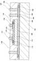
図1は本発明の第1の実施の形態を示す構造断面図である。支持基板となるICチップ101上に別のICチップ111がダイボンディングされてパッケージに内蔵されている。支持基板となるICチップ101とパッケージのサイズは同等である。
【0011】
ICチップ101上にはパッド102と,2層の表面保護膜103,104が形成されている。パッド102はICチップ101の内部集積回路と電気的に接続されている。表面保護膜103および104は,集積回路の表面保護のためのものであり,パッド102上に開口部を有する。さらに,パッド102に接続し表面保護膜104上に導体105,導体105に接続して柱状の導体106,導体106上に接続材料107が形成されている。
【0012】
導体105,106によりパッド102からパッケージの外部端子へ電気的に接続でき,接続材料107により,パッケージを外部基板(図示せず)に接続できる。すなわち,一連の接続されたパッド102,導体105,106,接続材料107により,ICチップ101の内部集積回路と外部基板とを電気的に接続できる。
【0013】
表面保護膜104上には,ダイボンディング材料108を介してICチップ111がダイボンディングされている。ICチップ111は,支持基板となるICチップ101とは別のチップであり,ICチップ101より小さく,かつ同一パッケージに内蔵できる程薄く研削されている。
【0014】
ICチップ111上にはパッド112と,2層の表面保護膜113,114が形成されている。パッド112はICチップ111の内部集積回路と電気的に接続されている。表面保護膜113および114は,集積回路の表面保護のためのものであり,パッド112上に開口部を有する。さらに,パッド112に接続し表面保護膜114上に導体115,導体115に接続して柱状の導体116,導体116上に接続材料117が形成されている。そして,樹脂130は全てのICチップの少なくとも集積回路形成面を封止している。
【0015】
導体115,116によりパッド112からパッケージの外部端子へ電気的に接続でき,接続材料117により,パッケージを外部基板へ接続できる。すなわち,一連の接続されたパッド112,導体115,116,接続材料117により,ICチップ111の内部集積回路とパッケージの外部基板とを電気的に接続できる。
【0016】
表面保護膜103,104および113,114は,それぞれICチップ101および111の表面保護膜である。ここでは表面保護膜103および113はシリコン酸化膜もしくはシリコン窒化膜とし,表面保護膜104および114はポリイミドなどの高分子樹脂からなる膜とする。これらの表面保護膜は単層構成でもよいが複合層構成にすることにより,ICチップ上の導体形成やダイボンディングなどの加工の影響,およびパッケージを基板へ接続した後の熱応力の影響から集積回路をより保護できる。
【0017】
導体105,115は,それぞれパッド102と導体106,パッド112と導体116を結ぶ導体配線である。ここではチタンおよび銅からなる複合層構成の金属材料によるものとする。この場合,チタン層はパッドや表面保護膜との密着性や拡散防止機能のために形成され,銅層は主として電気的な接続材料としての機能のために形成する。無論,単層構成でもよいし材料構成を問うものではない。複合層構成の場合の材料構成例については,クロム−銅,クロム−金,ニッケル−銅,ニッケル−金,チタン/タングステン−銅,チタン/タングステン−金等さまざまなものが考えられる。
【0018】
導体106,116は,それぞれ導体105,115からパッケージ外部へ電気的接続を施すための導体で,少なくも樹脂130よりその一部が露出している必要がある。材料としては電気抵抗の低い材料が好ましく銅,金,アルミニウムなどが挙げられる。
【0019】
なお,図1では支持基板となるICチップ以外の内蔵ICチップは,ICチップ111の1つしか示していないが,複数のICチップであってもよい。この点は,以下に述べる実施の形態についても同様である。ここで,支持基板となるICチップ101をロジック系チップとし,内蔵されるICチップ111をメモリ系チップとすれば,ロジック系とメモリ系の混載が可能となる。またICチップの組み合わせは上記に限定されるものではなく,メモリ系の半導体素子同士,ロジック系半導体素子同士でも可能である。
【0020】
図8は,図1に示した構造の半導体パッケージを実装基板に実装した図である。ICチップ101,111を内蔵した半導体装置100が,実装基板150に実装基板上配線151により実装されている。なお,図8では半導体装置100の上下は図1とは逆になっている。半導体装置100を実装基板150に実装することにより,ICチップ101,111が実装基板上配線151に電気的に接続される。半導体装置100単体の状態ではICチップ101,111間は電気的には直接接続されていないが,実装基板150に実装した状態では実装基板上配線151を介して,ICチップ101とICチップ111は接続されている。
【0021】
以下に,図9を参照しながら,ICチップ101にICチップ111を搭載する方法を説明する。まず,ICチップ101においては,パッド102,表面保護膜103,104,導体105,106が形成された状態,ICチップ111においては,パッド112,表面保護膜113,114,導体115,116が形成された状態のものを準備する。ここで,ICチップ101は既にダイシングされ個片化されたものでもダイシング前のウエハ状態でもかまわない。
【0022】
ICチップ101へICチップ111をダイボンディングする際,ICチップ101が個片化されたICチップの場合は,図9(1)に示すように,個片化されたICチップ199を個片化されたICチップ191上にダイボンディング材料108でボンディングすることになる。ICチップ101がダイシング前のウエハ状態であれば図9(2)に示すように,個片化されたICチップ199をウエハ181上にダイボンディング材料108でボンディングすることになる。
【0023】
半導体パッケージには可能限界までの小型化が要求されるので,ICチップ101とICチップ111は可能な限り薄く並行にダイボンディングされることが望まれる。したがって,ダイボンディング材料108は薄くかつ均一な厚さが得られるものが好ましい。ダイボンディング材料108は,銀を主材料とする導電性ペーストや液状ポリイミド,シート状接着剤などさまざまなものが考えられる。
【0024】
個片化されたICチップを支持基板となるICチップへ搭載する場合は,これら2つのICチップに傷が生じるなどの心配がない。一方,個片化されたICチップを個片化される前のウエハ状態のICへ搭載する場合は,以後の工程をウエハ単位で一括処理できるので製造が容易になるという利点がある。
【0025】
次に,図10を参照しながら,半導体パッケージの外部へ電気的接続を施すための柱状の導体106および116において,パッケージの同一表面に導体を露出させる方法について述べる。前述したICチップ101にICチップ111を搭載すると,その上に形成されている導体106および116は,一般に図10に示すように高さが不揃いとなる。柱状の導体106および116の形成は,厚膜レジストでパターンを形成しメッキにより行うか,既存の微細な柱状部品を接着・固定することにより行われる。しかし,ICチップ101にICチップ111を搭載した時に導体106および116の最上面が同一表面に均一に露出するように,上記の導体形成時に導体106および116の高さをあらかじめ調整するのは困難である。
【0026】
よって,ICチップ101にICチップ111を搭載し,導体106および116の高さが不揃いの状態で,両者の最上面より高い面1001まで樹脂130により封止する。次に,樹脂130を1002の面まで研磨もしくはエッチングする。この時,導体106および116も同時に研磨もしくはエッチングする。これにより,各IC上に形成された柱状の導体106および116を,パッケージの同一表面に露出することができる。
【0027】
次に,本発明で提供するMCP化された半導体装置の電気的試験方法について説明する。これには,半導体装置の状態により2つの方法が考えられる。1つは,MCP化された半導体装置が個片化された状態であり,その個片化された1つのパッケージ毎に試験する方法である。もう1つの方法は,支持基板となるICがウエハの状態であり,かつ内蔵されるICチップが搭載され樹脂封止され柱状導体が露出した時点で試験する方法である。
【0028】
前者の試験方法は,個別に試験を行うことができるので,確実に試験が行われ,不良品については判明した時点で良品と分別可能である。後者の試験方法は,いわゆるブロービング方式が応用可能で,前者の試験方法と比較すると特別な試験用ソケットなどの特殊な治具を準備する必要がない。いずれにしても,内蔵される各ICを個々に試験した後組み合わせるだけではなく,MCP化された半導体装置で電気的試験を行うことにより,内蔵される複数のIC間の電気的接続,および組み合わせて初めて確認可能な機能の試験が可能になる。
【0029】
以上より,本実施の形態によれば,以下に述べる多数の効果が得られる。インターポーザーを使用することなく,複数のICチップを内蔵できるMCPであり,かつそのパッケージサイズは内蔵されるICチップの中で最大のものと同サイズでよいため,実装基板上に高密度実装が可能になる。また,複数のICチップが半導体パッケージに内蔵され,全て樹脂封止されているので,パッケージ外部に別のICチップを装着したものに比較して耐湿性等における信頼性が高い。複数のICチップを同時に実装できるので,実装基板に対する実装加工工程が少なくなりコストが低減できる。実装基板に1つのMCPを実装することにより,内蔵された複数のICチップを同時に電気的に接続することができる。
【0030】
また,支持基板となるICが個片化された状態の場合は,個片化されたICチップ上に別の個片化されたICチップを搭載するので,個片化される前に隣接していたICチップに傷をつけるなどの不具合がなくなる。支持基板となるICがウエハ状態の場合は,ウエハ上に複数の個片化されたICチップを搭載し,以後の工程となる樹脂封止および導体露出,端子処理をウエハ単位で一括処理できるので,製造が容易になる。
【0031】
支持基板となるIC上に複数の個片化されたICチップを搭載し,樹脂封止後各IC上に形成された柱状の導体を樹脂とともに研磨しあるいはエッチングすることにより,容易に半導体パッケージの同一表面に柱状の導体を均一に露出させることができる。
【0032】
1つの半導体パッケージに複数のICチップが内蔵された状態で電気的検査を行う試験方法を採用することにより,確実に試験が行われるとともに不良品についてはその時点で良品と分別することが可能である。支持基板となるICがウエハの状態であり,他の個片化されたICチップを搭載し,樹脂封止し,支持基板となるICを個片化する前に電気的検査を行う試験方法の場合は,いわゆるブロービング方式が応用可能で前者の試験方法と比較して特別に試験用ソケットなど特殊な治具の準備を必要としない。MCP化された半導体装置で電気的試験を行うことにより,内蔵される複数のIC間の電気的接続,および組み合わせて初めて確認可能な機能の試験が可能になる。
【0033】
図2は,本発明の第2の実施の形態を示す構造断面図である。本実施の形態では,導体105の1つが導体205に代替されている。導体205はICチップ111のダイボンディング領域まで延長され,その上にICチップ111がダイボンディング材料208によりボンディングされている。ダイボンディング材料208は導電性を有する。
【0034】
このような構造により,ICチップ111の裏面は,接続材料107およびICチップ101の内部集積回路と,ダイボンディング材料208,導体205を介して電気的に接続されている。よって,図2で示す半導体装置を実装基板に接続すると,接続材料107,導体205,ダイボンディング材料208を介してICチップ111の裏面電位を固定できる。
【0035】
本実施の形態によれば,第1の実施の形態の効果に加えて,半導体パッケージに内蔵されるICチップの裏面電位を固定することができ,半導体装置の安定した機能が得られる。
【0036】
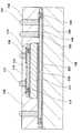
図3は,本発明の第3の実施の形態を示す構造断面図である。本実施の形態では,第1の実施の形態における導体105および115に代わり,導体305および315が設けられ,そして新たにICチップ111の側面に絶縁材料309が設けられている。導体305および315は延長され絶縁材料309の表面を介して接続されている。
【0037】
導体305および315が接続されたことにより,支持基板となるICチップ101と内蔵されるICチップ111がパッケージ内部で電気的に接続される。また,ICチップ101上に複数のICチップをダイボンディングする場合,それらのICチップにも導体305および315と同様の導体を設け,適宜配置することにより,支持基板以外の内蔵される複数のICチップ間を電気的に接続することができる。なお,本実施の形態においては導体116,接続材料117は必ずしも必要ではない。
【0038】
本実施の形態によれば,第1の実施の形態の効果に加えて,半導体パッケージに内蔵される複数のICチップ間の電気的接続を半導体パッケージ内部で施すことが可能である。これにより,内蔵されるICチップ間の電気的接続を考慮した配線を,半導体装置を接続する接続基板上に形成する必要がない。また,半導体パッケージに内蔵される複数のICチップ間の電気的接続がより短い配線を使用し施すことが可能になるため,半導体装置の高速化が図れる。
【0039】
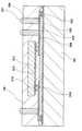
図4は,本発明の第4の実施の形態を示す構造断面図である。本実施の形態ではさらに,表面保護膜104に代わり表面保護膜104よりも厚みを増した表面保護膜404を設けている。そして,表面保護膜404は,ICチップ111と同等サイズの孔部,およびパッド102上に設けられた開口部を有する。ICチップ111は,孔部に埋め込まれてダイボンディングされる。導体405はパッド102に接続した後は表面保護膜404の表面上を延長し,導体415と接続している。ここで,表面保護膜404の材料としてはポリイミドなどの高分子樹脂を用いている。
【0040】
導体405および415が接続されたことにより,支持基板となるICチップ101と内蔵されるICチップ111がパッケージ内部で電気的接続される。また,ICチップ101上に複数のICチップをダイボンディングする場合,それら複数の内蔵されるICチップ間も,支持基板となるICチップの表面に形成される導体を介して電気的に接続される。さらに,厚みを増した表面保護膜404に孔部を設けその中にICチップ111を埋め込むようにしたことにより,支持基板となるICチップ101にダイボンディングされるICチップ111の厚さによって生じる段差を少なくとも第3の実施の形態に比較して改善できる。
【0041】
このような構造は,個片化されたICチップを個片化される前のウエハ状態のICへ搭載する製造方法を選択する場合に有利となる。というのは,ウエハおよびICチップ111の表面に同時に導体形成およびそのパターニングを施すことができ,導体405と415を電気的に接続する構造の形成が一括して行えるからである。また,半導体パッケージの内部の樹脂封止される面がより平坦化されるため,樹脂130による封止も容易になる。なお,本実施の形態においては導体116,接続材料117は必ずしも必要ではない。
【0042】
本実施の形態によれば,第3の実施の形態の効果に加えて,支持基板となるICチップにダイボンディングされるICチップの厚さによって生じる段差が改善されているため,支持基板となるICチップ上の導体と内蔵されるそれ以外のICチップ上の導体を電気的に接続する構造の形成が容易になる。また,樹脂封止も容易になる。
【0043】
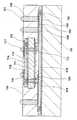
図5は,本発明の第5の実施の形態を示す構造断面図である。本実施の形態が前述の実施の形態と大きく異なる点は,支持基板となるICチップ101上に,別のICチップ511がフェイスダウンボンディングされてパッケージに内蔵されている点である。ICチップ511は,支持基板となるICチップ101とは別のチップであり,ICチップ101より小さく,かつ同一パッケージに内蔵できる程薄く研削されている。
【0044】
ICチップ511にはパッド512と,表面保護膜513が形成されている。パッド512はICチップ511の内部集積回路と電気的に接続されている。表面保護膜513は,集積回路の表面保護のためのものであり,ICチップ512表面を覆い,パッド512上に開口部を有する。さらに,パッド512に接続し表面保護膜513の外側に電極接続材料518が形成されている。電極接続材料518としては,例えばバンプ電極や印刷などで形成される導電性樹脂などを用いることができる。ICチップ101のパッド102に接続している導体505は,第1の実施の形態の導体105に比べ延長されて形成され,電極接続材料518と電気的に接続されている。
【0045】
導体505と電極接続材料518が接続されたことにより,支持基板となるICチップ101と内蔵されるICチップ511がパッケージ内部で電気的接続される。また,支持基板となるICチップ101以外の複数の内蔵されるチップ間も,支持基板となるICチップの表面に形成される導体を介して電気的接続される。また,ICチップ511は,電極接続材料518により外部端子と接続するため,前述の実施の形態で用いた導体115,116,接続材料117等が不要になる。また,導体115,116がないため,1層の表面保護膜513だけで十分となり,表面保護膜114も不要になる。
【0046】
本実施の形態によれば,第1の実施の形態の効果に加えて,半導体パッケージに内蔵される複数のICチップ間の電気的接続を半導体パッケージ内部で施すことが可能である。これにより,内蔵されるICチップ間の電気的接続を考慮した配線を,半導体装置を接続する接続基板上に形成する必要がない。また,半導体パッケージに内蔵される複数のICチップ間の電気的接続をより短い配線で行うことが可能になるため,半導体装置の高速化が図れる。さらに,前述の実施の形態に比べ,半導体パッケージに内蔵される,支持基板になるICチップ以外のICチップに対する加工が簡素化できる。
【0047】
図6は,本発明の第6の実施の形態を示す構造断面図である。本実施の形態も,第5の実施の形態と同様に,支持基板となるICチップ101上に,別のICチップ511がフェイスダウンボンディングされてパッケージに内蔵されている。ただし,本実施の形態では,ICチップ101上に新たに,パッド602,パッド602に接続して表面保護膜104上に導体605が形成されている。パッド602はICチップ101の内部集積回路と電気的に接続されている。表面保護膜103および104は,パッド602上に開口部を有する。導体605は,ここではICチップ101とICチップ511の間に形成されており,ICチップ511の電極接続材料518と電気的に接続されている。導体605は,導体105とは異なり,外部端子に接続可能な導体106および接続材料107とは接続されていない。パッド602は,導体605と電極接続材料518が接続されるのに好適な位置に配置される。
【0048】
パッド602,導体605を設け,導体605と電極接続材料518が接続されたことにより,支持基板となるICチップ101と内蔵されるICチップ511がパッケージ内部で電気的接続される。さらに,ICチップ101上に複数のICチップをボンディングする場合,それら複数の内蔵されるICチップ間を,導体605を介して電気的に接続することができる。
【0049】
本実施の形態によれば,第5の実施の形態の効果に加えて,支持基板になるICチップとそれ以外の半導体パッケージに内蔵されるICチップの間でそれぞれの内部集積回路の電気的接続が可能であり,配線の自由度が高まり,より高密度な内部配線構造を提供できる。
【0050】
図7は,本発明の第7の実施の形態を示す構造断面図である。本実施の形態も,第5,第6の実施の形態と同様に,支持基板となるICチップ101上に,別のICチップ711がフェイスダウンボンディングされてパッケージに内蔵されている。ただし,本実施の形態では,第5の実施の形態の構造に加えて,ICチップ711内部に,新たに貫通電極719を設ける。貫通電極719はICチップ711を貫通し,内部に導体720を有する。導体720は,ICチップ711の半導体基板とは絶縁されている。ここでは貫通電極719は貫通孔と貫通孔側壁に設けた導体720からなるものとして図示しているが,上記以外の構造であってもよい。例えば,ICチップ711を貫通する柱状の導体を設け,ICチップ711の半導体基板と絶縁するよう構成してもよい。
【0051】
ICチップ101に対向するICチップ711の表面には,パッド712,表面保護膜513,電極接続材料518が形成されている。パッド712は,貫通電極719に接続し,かつICチップ101の内部集積回路と電気的に接続されている。表面保護膜513は,ICチップ711表面を覆い,パッド712上に開口部を有する。電極接続材料518は,パッド712に接続し,かつICチップ101上の導体505にも接続している。
【0052】
また,ICチップ711の裏面には,裏面電極722と,2層の表面保護膜713,714が形成されている。裏面電極722は,貫通電極719に電気的に接続されている。表面保護膜713,714は,ICチップ711の裏面の形成された配線の表面保護のためのものであり,裏面電極722上に開口部を有する。さらに,裏面電極722に接続し表面保護膜714上に導体715,導体715に接続して柱状の導体116,導体116上に接続材料117が形成されている。
【0053】
上記のような構成により,貫通電極719の一端は電極接続材料518,導体505を介してICチップ101に接続されており,他端はパッケージ外部への導体と接続されている。これより,ICチップ711から貫通電極719を通して直接パッケージ外部へ電気的接続が可能になる。
【0054】
本実施の形態によれば,第5の実施の形態の効果に加えて,支持基板になるICチップとそれ以外の半導体パッケージに内蔵されるICチップの間でそれぞれのICの電気的接続が可能である。また,支持基板以外の内蔵されるICチップから,半導体パッケージ外部へ直接電気的接続が可能になる。これより,多ピン化された半導体パッケージを提供することができ,配線の自由度が高まる。
【0055】
上記では,接続材料107,117を設けた例について説明したが,導体106,116の表面は,樹脂130表面に露出しているため,接続材料107,117を省略した場合においても外部との電気的接続は可能である。本発明の効果は得られる。接続材料107,117を省略した場合には,より低コストの半導体装置を提供できるという利点がある。
【0056】
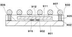
図11は本発明の第8の実施の形態を示す構造断面図である。これは,図17に示した従来のCSPに本発明を適用した例の1つである。支持基板となるICチップ801上に別のICチップ811がダイボンディングされてパッケージに内蔵されている。支持基板となるICチップ801とパッケージのサイズは同等である。
【0057】
ICチップ801上にはアルミ電極パッド802が形成されている。アルミ電極パッド802は,ICチップ801の内部集積回路と電気的に接続されている。アルミ電極パッド802に接続して,柱状の導体である銅ポスト805が形成されている。さらに,ICチップ801上には,接着シート808を介してICチップ811が固定されている。ICチップ811は,支持基板となるICチップ801とは別のチップであり,ICチップ801より小さく,かつ同一パッケージに内蔵できる程薄く研削されている。ICチップ811上にはアルミ電極パッド812が形成されている。アルミ電極パッド812は,ICチップ811の内部集積回路と電気的に接続されている。アルミ電極パッド812に接続して,金バンプ815が形成されている。
【0058】
樹脂830は,全てのICチップの少なくとも集積回路形成面を封止している。樹脂830上の所定位置,および銅ポスト805上,金バンプ815上には,表面に金,スズ等のメッキが施された再配線パターン806が間隔をおいて複数形成されている。再配線パターン806上には,外部接続端子用のハンダボール807が形成されている。
【0059】
銅ポスト805によりアルミ電極パッド802からパッケージの外部端子へ電気的に接続でき,ハンダボール807により,パッケージを外部基板へ接続できる。すなわち,一連の接続されたアルミ電極パッド802,銅ポスト805,再配線パターン806,ハンダボール807により,ICチップ801の内部集積回路とパッケージの外部基板とを電気的に接続できる。
【0060】
同様に,金バンプ815によりアルミ電極パッド812からパッケージの外部端子へ電気的に接続でき,ハンダボール807により,パッケージを外部基板へ接続できる。すなわち,一連の接続されたアルミ電極パッド812,金バンプ815,再配線パターン806,ハンダボール807により,ICチップ811の内部集積回路とパッケージの外部基板とを電気的に接続できる。また,再配線パターン806,ハンダボール807により,ICチップ801とICチップ811を接続することもできる。以上より,本実施の形態によれば,第1の実施の形態と同様の効果が得られる。
【0061】
以下に,図15を参照しながら,第8の実施の形態の製造方法の一例を示す。まず,ICチップ801においては,アルミ電極パッド802が形成された状態,ICチップ811においては,アルミ電極パッド812と,その上に金バンプ815が形成された状態のものを準備する。ここでは,ICチップ801については,個片化される前のウエハ状態の場合について説明する。図15(a)において,ウエハ881はICチップ801となる半導体素子が形成されたウエハであり,その上にはアルミ電極パッド802が形成されている。
【0062】
次に図15(b)に示すように,アルミ電極パッド802上に銅ポスト805を形成する。銅ポスト805の形成は,ウエハ881全面への金属膜の蒸着,感光性レジストの塗布,パターニング,銅メッキ,感光性レジスト除去,余分な金属膜の剥離の工程を順に行うことにより得られる。次に図15(c)に示すように,アルミ電極パッド812,金バンプ815が形成されたICチップ811を,接着シート808を用いてウエハ881に搭載する。
【0063】
その後,図15(d)に示すように,ウエハ881上の全てを樹脂830で封止し,保護する。この状態では,銅ポスト805,金バンプ815とも,樹脂830内部に埋まっている。次に図15(e)に示すように,樹脂830の上面を銅ポスト805,金バンプ815が露出するまで削る。
【0064】
次に図15(f)に示すように,樹脂830,銅ポスト805,金バンプ815上に再配線パターン806を形成する。再配線パターン806の形成は,樹脂830全面への金属膜の蒸着,感光性レジストの塗布,パターニング,銅メッキ,感光性レジスト除去,余分な金属膜の剥離,無電解スズ(あるいは金)メッキの工程を順に行うことにより得られる。
【0065】
次に図15(g)に示すように,再配線パターン806上にハンダボール807を形成する。最後にウエハをダイシングし,図15(h)に示すように個片化して第8の実施の形態のCSPが完成する。
【0066】
図12は本発明の第9の実施の形態を示す構造断面図である。これも,図17に示した従来のCSPに本発明を適用した例の1つである。第8の実施の形態と大きく異なる点は,支持基板となるICチップ801上に別のICチップ911がフェイスダウンボンディングされてパッケージに内蔵されている点である。支持基板となるICチップ801とパッケージのサイズは同等である。ICチップ911は,支持基板となるICチップ801とは別のチップであり,ICチップ801より小さく,かつ同一パッケージに内蔵できる程薄く研削されている。
【0067】
本実施の形態では,第8の実施の形態と比べ,アルミ電極パッド802に加え,アルミ電極パッド902が,ICチップ801上のICチップ911と対向する位置に形成されている。そして,アルミ電極パッド812に代わり,アルミ電極パッド912が,ICチップ911のICチップ801と対向する面に形成されている。アルミ電極パッド902とアルミ電極パッド912の間には,両者と接続して金バンプ915が形成されている。このように,ICチップ911をボンディングするにあたり,接着シート808を用いない構成となっている。また,ICチップ911と再配線パターン806を直接接続する導体はない。その他の構成は第8の実施の形態と同じである。
【0068】
アルミ電極パッド802,902は,ICチップ801の内部集積回路と電気的に接続されている。アルミ電極パッド912は,ICチップ911の内部集積回路と電気的に接続されている。よって,ICチップ801とICチップ911の内部集積回路は,パッケージ内部で電気的に接続される。ICチップ911を外部基板に接続したい場合は,ICチップ801および再配線パターン806,ハンダボール807を介して接続することが可能である。本実施の形態では,接着シート808を用いないため,安価なCSPを提供することができる。以上より,本実施の形態によれば,第5の実施の形態と同様の効果が得られる。
【0069】
以下に,図16を参照しながら,第9の実施の形態の製造方法の一例を示す。まず,ICチップ801においては,アルミ電極パッド802,902が形成された状態,ICチップ911においては,アルミ電極パッド912と,その上に金バンプ915が形成された状態のものを準備する。ここでは,ICチップ801については,個片化される前のウエハ状態の場合について説明する。図16(a)において,ウエハ881はICチップ801となる半導体素子が形成されたウエハであり,その上にはアルミ電極パッド802,902が形成されている。
【0070】
次に図16(b)に示すように,アルミ電極パッド802上に銅ポスト805を形成する。銅ポスト805の形成は,図15(b)での説明と同様に行う。次に図16(c)に示すように,アルミ電極パッド912,金バンプ915が形成されたICチップ911を,フェイスダウンボンディングによりウエハ881に搭載する。その後,図16(d)に示すように,ウエハ881上の全てを樹脂830で封止する。次に図16(e)に示すように,樹脂830の上面を銅ポスト805が露出するまで削る。
【0071】
次に図16(f)に示すように,樹脂830,銅ポスト805上に再配線パターン806を形成する。再配線パターン806の形成は,図15(f)での説明と同様に行う。その後の図16(g),図16(h)に示す工程は,図15(g),図15(h)で説明したものと同じである。以上のようにして,第9の実施の形態のCSPが完成する。
【0072】
図13は本発明の第10の実施の形態を示す構造断面図である。これは,第9の実施の形態からハンダボール807を無くしたものである。その他の構成は第9の実施の形態と同じである。ハンダボール807を省くことにより,更なる低コストのCSPを提供することができる。
【0073】
図14は本発明の第11の実施の形態を示す構造断面図である。これは,フェイスダウンボンディングにより内蔵されるICチップの数を2つにしたものである。その他の構成は第9の実施の形態と同じである。内蔵されるICチップ921,931は,同一のものでも,別のものでも構わない。また,内蔵されるICチップの数は,2つではなく,3つ以上でも構わない。内蔵されるICチップの数を増やすことにより,更なる高機能なCSPを提供することができる。
【0074】
以上,添付図面を参照しながら本発明にかかる好適な実施形態について説明したが,本発明はかかる例に限定されないことは言うまでもない。当業者であれば,特許請求の範囲に記載された技術的思想の範疇内において,各種の変更例または修正例に想到し得ることは明らかであり,それらについても当然に本発明の技術的範囲に属するものと了解される。
【0075】
【発明の効果】
以上,詳細に説明したように本発明によれば,インターポーザーを内蔵しないCSPにおいてMCP化が可能な半導体装置を提供できる。
【図面の簡単な説明】
【図1】 本発明の第1の実施の形態を示す構造断面図である。
【図2】 本発明の第2の実施の形態を示す構造断面図である。
【図3】 本発明の第3の実施の形態を示す構造断面図である。
【図4】 本発明の第4の実施の形態を示す構造断面図である。
【図5】 本発明の第5の実施の形態を示す構造断面図である。
【図6】 本発明の第6の実施の形態を示す構造断面図である。
【図7】 本発明の第7の実施の形態を示す構造断面図である。
【図8】 本発明の第1の実施の形態に係る半導体パッケージを実装基板に実装した図である。
【図9】 本発明の第1の実施の形態に係る半導体装置の製造方法を説明する図である。
【図10】 本発明の第1の実施の形態に係る半導体装置の製造方法を説明する図である。
【図11】 本発明の第8の実施の形態を示す構造断面図である。
【図12】 本発明の第9の実施の形態を示す構造断面図である。
【図13】 本発明の第10の実施の形態を示す構造断面図である。
【図14】 本発明の第11の実施の形態を示す構造断面図である。
【図15】 本発明の第8の実施の形態に係る半導体装置の製造方法を説明する図である。
【図16】 本発明の第9の実施の形態に係る半導体装置の製造方法を説明する図である。
【図17】 従来の半導体装置を示す構造断面図である。
【符号の説明】
100 半導体装置
101,111 ICチップ
102,112 パッド
103,104,113,114 表面保護膜
105,106,115,116 導体
107,117 接続材料
108 ダイボンディング材料
130 樹脂[0001]
BACKGROUND OF THE INVENTION
The present invention uses a chip size package to make a multichip.For semiconductor devicesIt is related.
[0002]
[Prior art]
With the recent miniaturization of electronic devices, various methods enabling high-density mounting are being studied when mounting semiconductor devices. Among these methods, there are methods for reducing the size of semiconductor devices and increasing the density of mounting multiple components. As for miniaturization of semiconductor devices, miniaturization of semiconductor packages incorporating IC chips has been studied, and there is a semiconductor package called a chip size package (hereinafter abbreviated as CSP) having substantially the same size as the IC chip. For increasing the density of mounting of multiple components, a multichip module (hereinafter abbreviated as MCM) or a multichip package (hereinafter abbreviated as MCP) in which a plurality of IC chips and other components are built in a single module or package. )
[0003]
An example of the structure of a conventional CSP is shown in FIG. An
[0004]
A plurality of
[0005]
[Problems to be solved by the invention]
However, among the CSPs described above, a CSP that does not incorporate an intermediate substrate called an interposer cannot incorporate a plurality of IC chips due to its external size and structure, and it has been difficult to make an MCP. For this reason, when a plurality of semiconductor packages on a mounting board are electrically wired, the wiring length becomes long, which is an obstacle not only in high-density mounting but also in speeding up the final electronic equipment.
[0006]
On the other hand, in a semiconductor package with a built-in interposer, a plurality of IC chips can be mounted on the interposer. However, the package size is larger than the IC chip, and the package cost is high because the interposer is built-in. There was a problem.
[0007]
The present invention has been made in view of such problems, and the object of the present invention is to enable MCP in a CSP that does not incorporate an interposer.Semiconductor devicesIt is to provide.
[0008]
[Means for Solving the Problems]
In order to solve the above problems, the present inventionThe semiconductor device includes a first surface having a main surface.I cA chip, a pad provided on a main surface of the first IC chip, and a first part so as to expose a part of the padI cA second surface having an insulating film provided on the main surface of the chip, wiring extending from the pad onto the insulating film, a first surface on which an integrated circuit is formed, and a second surface facing the first surface Is provided on the insulating film so as to face the insulating film.I cChip and secondI cA second surface provided on the first surface of the chip;I cA first columnar conductor electrically connected to the integrated circuit formed on the first surface of the chip; a second columnar conductor provided on the wiring; and provided immediately above the tip of the first columnar conductor. A first external terminal; a second external terminal provided immediately above the tip of the second columnar conductor; a side surface of the first and second columnar conductors; an insulating film;I cAnd a resin covering the first surface and the side surface of the chip.
[0009]
DETAILED DESCRIPTION OF THE INVENTION
Hereinafter, embodiments of the present invention will be described in detail with reference to the drawings. In the following description and the accompanying drawings, components having substantially the same function and configuration are denoted by the same reference numerals, and redundant description is omitted.
[0010]
FIG. 1 is a structural cross-sectional view showing a first embodiment of the present invention. Another
[0011]
A
[0012]
The
[0013]
An
[0014]
A
[0015]
The
[0016]
The surface
[0017]
The
[0018]
The
[0019]
In FIG. 1, only one
[0020]
FIG. 8 is a diagram in which the semiconductor package having the structure shown in FIG. 1 is mounted on a mounting substrate. The semiconductor device 100 incorporating the IC chips 101 and 111 is mounted on the mounting
[0021]
Hereinafter, a method of mounting the
[0022]
When the
[0023]
Since the semiconductor package is required to be miniaturized to the limit possible, it is desired that the
[0024]
When the separated IC chip is mounted on the IC chip as the support substrate, there is no concern that the two IC chips are damaged. On the other hand, when an individualized IC chip is mounted on an IC in a wafer state before being separated into individual pieces, there is an advantage that the subsequent processes can be collectively processed in units of wafers, thereby facilitating manufacturing.
[0025]
Next, a method of exposing the conductors on the same surface of the package in the
[0026]
Therefore, the
[0027]
Next, an electrical test method for an MCP semiconductor device provided in the present invention will be described. There are two methods for this depending on the state of the semiconductor device. One is a state in which an MCP semiconductor device is singulated, and a test is performed for each singulated package. The other method is a test method in which an IC serving as a support substrate is in a wafer state, and a built-in IC chip is mounted, resin-sealed, and a columnar conductor is exposed.
[0028]
Since the former test method can be tested individually, the test is performed reliably, and defective products can be separated from non-defective products when they are identified. The latter test method can be applied to the so-called blowing method, and it is not necessary to prepare a special jig such as a special test socket as compared with the former test method. In any case, it is not only combined after individually testing each built-in IC, but by conducting an electrical test on the MCP-made semiconductor device, the electrical connection and combination between a plurality of built-in ICs It is possible to test functions that can be confirmed for the first time.
[0029]
As described above, according to the present embodiment, a number of effects described below can be obtained. Since it is an MCP that can incorporate multiple IC chips without using an interposer, and the package size may be the same as the largest IC chip built-in, high-density mounting on the mounting board is possible. It becomes possible. In addition, since a plurality of IC chips are built in the semiconductor package and all are sealed with resin, reliability in moisture resistance and the like is higher than that in which another IC chip is mounted outside the package. Since a plurality of IC chips can be mounted at the same time, the number of mounting processes for the mounting substrate is reduced, and the cost can be reduced. By mounting one MCP on the mounting substrate, a plurality of built-in IC chips can be electrically connected simultaneously.
[0030]
In addition, when the IC as the support substrate is separated, another IC chip is mounted on the separated IC chip, so that the adjacent IC chip is separated before being separated. This eliminates problems such as scratching the IC chip. When the IC as the support substrate is in a wafer state, a plurality of individual IC chips can be mounted on the wafer, and the subsequent steps of resin sealing, conductor exposure, and terminal processing can be performed in batch units. , Manufacturing becomes easier.
[0031]
A plurality of individual IC chips are mounted on an IC serving as a support substrate, and after sealing the resin, the columnar conductor formed on each IC is polished or etched together with the resin, so that the semiconductor package can be easily formed. Columnar conductors can be uniformly exposed on the same surface.
[0032]
By adopting a test method that conducts electrical inspection with multiple IC chips built into a single semiconductor package, it is possible to ensure that the test is performed and that defective products can be separated from non-defective products at that time. is there. A test method in which an IC serving as a support substrate is in a wafer state, and another IC chip is mounted, resin-sealed, and an electrical inspection is performed before the IC serving as a support substrate is separated. In this case, the so-called blowing method can be applied, and special jigs such as test sockets are not required compared to the former test method. By performing an electrical test on a semiconductor device that has been made into an MCP, it is possible to test electrical functions between a plurality of built-in ICs and functions that can be confirmed only in combination.
[0033]
FIG. 2 is a structural cross-sectional view showing a second embodiment of the present invention. In the present embodiment, one of the
[0034]
With such a structure, the back surface of the
[0035]
According to the present embodiment, in addition to the effects of the first embodiment, the back surface potential of the IC chip incorporated in the semiconductor package can be fixed, and a stable function of the semiconductor device can be obtained.
[0036]
FIG. 3 is a structural cross-sectional view showing a third embodiment of the present invention. In the present embodiment,
[0037]
By connecting the
[0038]
According to the present embodiment, in addition to the effects of the first embodiment, electrical connection between a plurality of IC chips built in the semiconductor package can be made inside the semiconductor package. As a result, it is not necessary to form a wiring considering the electrical connection between the built-in IC chips on the connection substrate to which the semiconductor device is connected. In addition, since the electrical connection between the plurality of IC chips incorporated in the semiconductor package can be performed using a shorter wiring, the speed of the semiconductor device can be increased.
[0039]
FIG. 4 is a structural cross-sectional view showing a fourth embodiment of the present invention. In this embodiment, a surface
[0040]
By connecting the
[0041]
Such a structure is advantageous when selecting a manufacturing method in which an individualized IC chip is mounted on an IC in a wafer state before being individualized. This is because conductor formation and patterning can be simultaneously performed on the wafer and the surface of the
[0042]
According to the present embodiment, in addition to the effects of the third embodiment, the level difference caused by the thickness of the IC chip die-bonded to the IC chip serving as the support substrate is improved, so that the support substrate is obtained. It is easy to form a structure for electrically connecting the conductor on the IC chip and the conductor on the other IC chip to be built therein. Also, resin sealing becomes easy.
[0043]
FIG. 5 is a structural cross-sectional view showing a fifth embodiment of the present invention. The present embodiment is greatly different from the above-described embodiment in that another
[0044]
A
[0045]
By connecting the
[0046]
According to the present embodiment, in addition to the effects of the first embodiment, electrical connection between a plurality of IC chips built in the semiconductor package can be made inside the semiconductor package. As a result, it is not necessary to form a wiring considering the electrical connection between the built-in IC chips on the connection substrate to which the semiconductor device is connected. In addition, since it is possible to make electrical connection between a plurality of IC chips built in the semiconductor package with shorter wiring, the speed of the semiconductor device can be increased. Further, as compared with the above-described embodiment, the processing for IC chips other than the IC chip to be a support substrate built in the semiconductor package can be simplified.
[0047]
FIG. 6 is a structural cross-sectional view showing a sixth embodiment of the present invention. Similarly to the fifth embodiment, in this embodiment, another
[0048]
By providing the
[0049]
According to the present embodiment, in addition to the effects of the fifth embodiment, electrical connection of each internal integrated circuit between the IC chip serving as the support substrate and the IC chip incorporated in the other semiconductor package. This increases the degree of freedom of wiring and provides a higher-density internal wiring structure.
[0050]
FIG. 7 is a structural cross-sectional view showing a seventh embodiment of the present invention. Similarly to the fifth and sixth embodiments, in this embodiment, another
[0051]
On the surface of the
[0052]
Further, on the back surface of the
[0053]
With the configuration described above, one end of the through electrode 719 is connected to the
[0054]
According to the present embodiment, in addition to the effects of the fifth embodiment, each IC can be electrically connected between the IC chip serving as the support substrate and the IC chip incorporated in the other semiconductor package. It is. In addition, an electrical connection can be made directly from the built-in IC chip other than the support substrate to the outside of the semiconductor package. As a result, a multi-pin semiconductor package can be provided, and the degree of freedom of wiring is increased.
[0055]
In the above, the example in which the
[0056]
FIG. 11 is a structural cross-sectional view showing an eighth embodiment of the present invention. This is one example in which the present invention is applied to the conventional CSP shown in FIG. Another
[0057]
An
[0058]
The
[0059]
A
[0060]
Similarly, the gold bumps 815 can be electrically connected from the
[0061]
An example of the manufacturing method according to the eighth embodiment will be described below with reference to FIG. First, the
[0062]
Next, as shown in FIG. 15B, a
[0063]
Thereafter, as shown in FIG. 15D, everything on the
[0064]
Next, as shown in FIG. 15 (f), a
[0065]
Next, as shown in FIG. 15G,
[0066]
FIG. 12 is a structural sectional view showing a ninth embodiment of the present invention. This is also one example in which the present invention is applied to the conventional CSP shown in FIG. A major difference from the eighth embodiment is that another
[0067]
In the present embodiment, compared to the eighth embodiment, in addition to the
[0068]
The
[0069]
An example of the manufacturing method according to the ninth embodiment will be described below with reference to FIG. First, the
[0070]
Next, as shown in FIG. 16B, a
[0071]
Next, as shown in FIG. 16F, a
[0072]
FIG. 13 is a structural cross-sectional view showing a tenth embodiment of the present invention. This is obtained by eliminating the
[0073]
FIG. 14 is a structural sectional view showing an eleventh embodiment of the present invention. In this case, the number of IC chips incorporated by face-down bonding is two. Other configurations are the same as those of the ninth embodiment. The built-in
[0074]
As mentioned above, although preferred embodiment concerning this invention was described referring an accompanying drawing, it cannot be overemphasized that this invention is not limited to this example. It is obvious for those skilled in the art that various changes or modifications can be conceived within the scope of the technical idea described in the claims. It is understood that it belongs to.
[0075]
【The invention's effect】
As described above in detail, according to the present invention, MCP can be implemented in a CSP that does not incorporate an interposer.Semiconductor devicesCan be provided.
[Brief description of the drawings]
FIG. 1 is a structural cross-sectional view showing a first embodiment of the present invention.
FIG. 2 is a structural cross-sectional view showing a second embodiment of the present invention.
FIG. 3 is a structural cross-sectional view showing a third embodiment of the present invention.
FIG. 4 is a structural sectional view showing a fourth embodiment of the present invention.
FIG. 5 is a structural cross-sectional view showing a fifth embodiment of the present invention.
FIG. 6 is a structural sectional view showing a sixth embodiment of the present invention.
FIG. 7 is a structural cross-sectional view showing a seventh embodiment of the present invention.
FIG. 8 is a diagram in which the semiconductor package according to the first embodiment of the present invention is mounted on a mounting substrate.
FIG. 9 is a diagram for explaining the method for manufacturing the semiconductor device according to the first embodiment of the invention.
FIG. 10 is a diagram for explaining the method for manufacturing the semiconductor device according to the first embodiment of the invention.
FIG. 11 is a structural sectional view showing an eighth embodiment of the present invention.
FIG. 12 is a structural sectional view showing a ninth embodiment of the present invention.
FIG. 13 is a structural sectional view showing a tenth embodiment of the present invention.
FIG. 14 is a structural sectional view showing an eleventh embodiment of the present invention.
FIG. 15 illustrates a method for manufacturing a semiconductor device according to an eighth embodiment of the present invention.
FIG. 16 illustrates a method for manufacturing a semiconductor device according to a ninth embodiment of the present invention.
FIG. 17 is a structural cross-sectional view showing a conventional semiconductor device.
[Explanation of symbols]
100 Semiconductor device
101,111 IC chip
102,112 pad
103, 104, 113, 114 Surface protective film
105, 106, 115, 116 conductors
107,117 connecting material
108 Die bonding materials
130 resin
Claims (2)
Translated fromJapanese前記第1のICチップの主表面上に設けられるパッドと、
前記パッドの一部を露出するように、前記第1のICチップの前記主表面上に設けられる絶縁膜と、
前記パッドから前記絶縁膜上に延在する配線と、
集積回路が形成された第1面と該第1面と対向する第2面とを有し、該第2面が前記絶縁膜と対向するように、前記絶縁膜上に設けられる第2のICチップと、
前記第2のICチップの前記第1面上に設けられ、該第2のICチップの該第1面に形成された前記集積回路と電気的に接続される第1の柱状導体と、
前記配線上に設けられる第2の柱状導体と、
前記第1の柱状導体の先端の真上に設けられる第1の外部端子と、
前記第2の柱状導体の先端の真上に設けられる第2の外部端子と、
前記第1及び第2の柱状導体の側面と前記絶縁膜と前記第2のICチップの前記第1面及び側面とを覆う樹脂とを備えたことを特徴とする半導体装置。A first IC chip having a main surface;
A pad provided on the main surface of the first IC chip;
Aninsulating film provided on the main surface ofthe firstICchipso as to expose a part of the pad;
Wiring extending on the insulating film from the pad;
And a second surface facing the first surface and the first surface on which an integrated circuit is formed, as said second surface is opposite to theinsulating film, a second IC providedon the insulating film Chips,
A first columnar conductor provided on the first surface of the second IC chip and electrically connected to the integrated circuit formed on the first surface of the second IC chip;
A second columnar conductor provided on thewiring ;
A firstexternal terminal provideddirectly above the tipof the first columnar conductor;
A secondexternal terminal provideddirectly above the tipof the second columnar conductor;
The semiconductordevice characterizedby comprising a resin covering the first surface and side surfaces of the side surface ofthe first and second columnar conductor andthe insulating film and the second IC chip.
Priority Applications (3)
| Application Number | Priority Date | Filing Date | Title |
|---|---|---|---|
| JP2000071027AJP3772066B2 (en) | 2000-03-09 | 2000-03-09 | Semiconductor device |
| US09/797,907US6765299B2 (en) | 2000-03-09 | 2001-03-05 | Semiconductor device and the method for manufacturing the same |
| US10/856,933US7528005B2 (en) | 2000-03-09 | 2004-06-01 | Method of manufacturing chip size package semiconductor device without intermediate substrate |
Applications Claiming Priority (1)
| Application Number | Priority Date | Filing Date | Title |
|---|---|---|---|
| JP2000071027AJP3772066B2 (en) | 2000-03-09 | 2000-03-09 | Semiconductor device |
Related Child Applications (2)
| Application Number | Title | Priority Date | Filing Date |
|---|---|---|---|
| JP2003323553ADivisionJP3999720B2 (en) | 2003-09-16 | 2003-09-16 | Semiconductor device and manufacturing method thereof |
| JP2004003385ADivisionJP3923944B2 (en) | 2004-01-08 | 2004-01-08 | Semiconductor device |
Publications (2)
| Publication Number | Publication Date |
|---|---|
| JP2001257310A JP2001257310A (en) | 2001-09-21 |
| JP3772066B2true JP3772066B2 (en) | 2006-05-10 |
Family
ID=18589678
Family Applications (1)
| Application Number | Title | Priority Date | Filing Date |
|---|---|---|---|
| JP2000071027AExpired - Fee RelatedJP3772066B2 (en) | 2000-03-09 | 2000-03-09 | Semiconductor device |
Country Status (2)
| Country | Link |
|---|---|
| US (2) | US6765299B2 (en) |
| JP (1) | JP3772066B2 (en) |
Families Citing this family (163)
| Publication number | Priority date | Publication date | Assignee | Title |
|---|---|---|---|---|
| US6642136B1 (en)* | 2001-09-17 | 2003-11-04 | Megic Corporation | Method of making a low fabrication cost, high performance, high reliability chip scale package |
| US6710454B1 (en)* | 2000-02-16 | 2004-03-23 | Micron Technology, Inc. | Adhesive layer for an electronic apparatus having multiple semiconductor devices |
| JP3917344B2 (en)* | 2000-03-27 | 2007-05-23 | 株式会社東芝 | Semiconductor device and method for mounting semiconductor device |
| KR100583491B1 (en)* | 2000-04-07 | 2006-05-24 | 앰코 테크놀로지 코리아 주식회사 | Semiconductor package and manufacturing method |
| US7247932B1 (en) | 2000-05-19 | 2007-07-24 | Megica Corporation | Chip package with capacitor |
| JP4505983B2 (en)* | 2000-12-01 | 2010-07-21 | 日本電気株式会社 | Semiconductor device |
| TW577152B (en) | 2000-12-18 | 2004-02-21 | Hitachi Ltd | Semiconductor integrated circuit device |
| US6815324B2 (en)* | 2001-02-15 | 2004-11-09 | Megic Corporation | Reliable metal bumps on top of I/O pads after removal of test probe marks |
| JP2002252318A (en)* | 2001-02-27 | 2002-09-06 | Nec Kansai Ltd | Chip-type semiconductor device |
| TWI313507B (en) | 2002-10-25 | 2009-08-11 | Megica Corporatio | Method for assembling chips |
| US7498196B2 (en) | 2001-03-30 | 2009-03-03 | Megica Corporation | Structure and manufacturing method of chip scale package |
| JP4593835B2 (en)* | 2001-07-04 | 2010-12-08 | パナソニック株式会社 | Semiconductor device and manufacturing method thereof |
| US6759275B1 (en) | 2001-09-04 | 2004-07-06 | Megic Corporation | Method for making high-performance RF integrated circuits |
| US6613606B1 (en) | 2001-09-17 | 2003-09-02 | Magic Corporation | Structure of high performance combo chip and processing method |
| US7099293B2 (en) | 2002-05-01 | 2006-08-29 | Stmicroelectronics, Inc. | Buffer-less de-skewing for symbol combination in a CDMA demodulator |
| TW550997B (en) | 2001-10-18 | 2003-09-01 | Matsushita Electric Industrial Co Ltd | Module with built-in components and the manufacturing method thereof |
| JP3861669B2 (en)* | 2001-11-22 | 2006-12-20 | ソニー株式会社 | Manufacturing method of multichip circuit module |
| WO2003049184A1 (en)* | 2001-12-07 | 2003-06-12 | Fujitsu Limited | Semiconductor device and method for manufacturing the same |
| TWI255001B (en)* | 2001-12-13 | 2006-05-11 | Matsushita Electric Industrial Co Ltd | Metal wiring substrate, semiconductor device and the manufacturing method thereof |
| TW584950B (en) | 2001-12-31 | 2004-04-21 | Megic Corp | Chip packaging structure and process thereof |
| US6673698B1 (en) | 2002-01-19 | 2004-01-06 | Megic Corporation | Thin film semiconductor package utilizing a glass substrate with composite polymer/metal interconnect layers |
| TW517361B (en) | 2001-12-31 | 2003-01-11 | Megic Corp | Chip package structure and its manufacture process |
| TW544882B (en) | 2001-12-31 | 2003-08-01 | Megic Corp | Chip package structure and process thereof |
| TW503496B (en) | 2001-12-31 | 2002-09-21 | Megic Corp | Chip packaging structure and manufacturing process of the same |
| TW577160B (en) | 2002-02-04 | 2004-02-21 | Casio Computer Co Ltd | Semiconductor device and manufacturing method thereof |
| US6867500B2 (en)* | 2002-04-08 | 2005-03-15 | Micron Technology, Inc. | Multi-chip module and methods |
| US20030218246A1 (en)* | 2002-05-22 | 2003-11-27 | Hirofumi Abe | Semiconductor device passing large electric current |
| JP3529050B2 (en) | 2002-07-12 | 2004-05-24 | 沖電気工業株式会社 | Method for manufacturing semiconductor device |
| WO2004015771A2 (en)* | 2002-08-09 | 2004-02-19 | Casio Computer Co., Ltd. | Semiconductor device and method of manufacturing the same |
| US6987031B2 (en)* | 2002-08-27 | 2006-01-17 | Micron Technology, Inc. | Multiple chip semiconductor package and method of fabricating same |
| JP2004140037A (en) | 2002-10-15 | 2004-05-13 | Oki Electric Ind Co Ltd | Semiconductor device and its manufacturing process |
| US7285867B2 (en)* | 2002-11-08 | 2007-10-23 | Casio Computer Co., Ltd. | Wiring structure on semiconductor substrate and method of fabricating the same |
| JP4016825B2 (en)* | 2002-12-09 | 2007-12-05 | ソニー株式会社 | Manufacturing method of semiconductor device |
| JP2004193404A (en)* | 2002-12-12 | 2004-07-08 | Alps Electric Co Ltd | Circuit module and its manufacturing method |
| US7388294B2 (en)* | 2003-01-27 | 2008-06-17 | Micron Technology, Inc. | Semiconductor components having stacked dice |
| JP3740469B2 (en)* | 2003-01-31 | 2006-02-01 | 株式会社東芝 | Semiconductor device and manufacturing method of semiconductor device |
| DE10320579A1 (en)* | 2003-05-07 | 2004-08-26 | Infineon Technologies Ag | Semiconductor wafer having an upper side, semiconductor chip positions with integrated circuits for first chips, central and edge regions and an equalizing layer useful in semiconductor technology |
| JP3968051B2 (en)* | 2003-05-14 | 2007-08-29 | 富士通株式会社 | Semiconductor device and manufacturing method thereof, and semiconductor device precursor and manufacturing method thereof |
| KR20050001159A (en)* | 2003-06-27 | 2005-01-06 | 삼성전자주식회사 | Multi-chip package having a plurality of flip chips and fabrication method thereof |
| US20040264148A1 (en)* | 2003-06-27 | 2004-12-30 | Burdick William Edward | Method and system for fan fold packaging |
| JP2005123463A (en) | 2003-10-17 | 2005-05-12 | Seiko Epson Corp | Semiconductor device and manufacturing method thereof, semiconductor device module, circuit board, and electronic device |
| US7394161B2 (en)* | 2003-12-08 | 2008-07-01 | Megica Corporation | Chip structure with pads having bumps or wirebonded wires formed thereover or used to be tested thereto |
| JP4599834B2 (en)* | 2003-12-12 | 2010-12-15 | ソニー株式会社 | Semiconductor device and manufacturing method thereof |
| JP3953027B2 (en) | 2003-12-12 | 2007-08-01 | ソニー株式会社 | Semiconductor device and manufacturing method thereof |
| US20050133933A1 (en)* | 2003-12-19 | 2005-06-23 | Advanpack Solutions Pte. Ltd. | Various structure/height bumps for wafer level-chip scale package |
| JP4271590B2 (en)* | 2004-01-20 | 2009-06-03 | 新光電気工業株式会社 | Semiconductor device and manufacturing method thereof |
| JP4055717B2 (en)* | 2004-01-27 | 2008-03-05 | カシオ計算機株式会社 | Semiconductor device and manufacturing method thereof |
| JP4527991B2 (en)* | 2004-01-28 | 2010-08-18 | 株式会社日立製作所 | Multi-chip module manufacturing method |
| JP2005332896A (en) | 2004-05-19 | 2005-12-02 | Oki Electric Ind Co Ltd | Semiconductor device, manufacturing method thereof, chip size package, and manufacturing method thereof |
| JP2006005101A (en) | 2004-06-16 | 2006-01-05 | Rohm Co Ltd | Semiconductor device |
| US7129572B2 (en)* | 2004-08-18 | 2006-10-31 | Chung-Cheng Wang | Submember mounted on a chip of electrical device for electrical connection |
| JP4800606B2 (en)* | 2004-11-19 | 2011-10-26 | Okiセミコンダクタ株式会社 | Method for manufacturing element-embedded substrate |
| JP2006173232A (en)* | 2004-12-14 | 2006-06-29 | Casio Comput Co Ltd | Semiconductor device and manufacturing method thereof |
| JP2006179570A (en) | 2004-12-21 | 2006-07-06 | Renesas Technology Corp | Method of manufacturing semiconductor device |
| US8294279B2 (en) | 2005-01-25 | 2012-10-23 | Megica Corporation | Chip package with dam bar restricting flow of underfill |
| JP4659488B2 (en) | 2005-03-02 | 2011-03-30 | Okiセミコンダクタ株式会社 | Semiconductor device and manufacturing method thereof |
| JP4731191B2 (en)* | 2005-03-28 | 2011-07-20 | 富士通セミコンダクター株式会社 | Semiconductor device and manufacturing method of semiconductor device |
| US7468545B2 (en)* | 2005-05-06 | 2008-12-23 | Megica Corporation | Post passivation structure for a semiconductor device and packaging process for same |
| US7582556B2 (en) | 2005-06-24 | 2009-09-01 | Megica Corporation | Circuitry component and method for forming the same |
| TWI290375B (en)* | 2005-07-15 | 2007-11-21 | Via Tech Inc | Die pad arrangement and bumpless chip package applying the same |
| CN100447997C (en)* | 2005-09-28 | 2008-12-31 | 王忠诚 | an electronic device |
| JP4395775B2 (en)* | 2005-10-05 | 2010-01-13 | ソニー株式会社 | Semiconductor device and manufacturing method thereof |
| JP4851794B2 (en) | 2006-01-10 | 2012-01-11 | カシオ計算機株式会社 | Semiconductor device |
| JP4876618B2 (en)* | 2006-02-21 | 2012-02-15 | セイコーエプソン株式会社 | Semiconductor device and manufacturing method of semiconductor device |
| US7993972B2 (en)* | 2008-03-04 | 2011-08-09 | Stats Chippac, Ltd. | Wafer level die integration and method therefor |
| TWI335658B (en)* | 2006-08-22 | 2011-01-01 | Advanced Semiconductor Eng | Stacked structure of chips and wafer structure for making same |
| KR100770934B1 (en)* | 2006-09-26 | 2007-10-26 | 삼성전자주식회사 | Semiconductor package and semiconductor system package using the same |
| JP2008091795A (en)* | 2006-10-04 | 2008-04-17 | Shinko Electric Ind Co Ltd | Semiconductor device and manufacturing method thereof |
| US8133762B2 (en) | 2009-03-17 | 2012-03-13 | Stats Chippac, Ltd. | Semiconductor device and method of providing z-interconnect conductive pillars with inner polymer core |
| US8193034B2 (en) | 2006-11-10 | 2012-06-05 | Stats Chippac, Ltd. | Semiconductor device and method of forming vertical interconnect structure using stud bumps |
| US8174119B2 (en) | 2006-11-10 | 2012-05-08 | Stats Chippac, Ltd. | Semiconductor package with embedded die |
| JP4480710B2 (en)* | 2006-12-04 | 2010-06-16 | Okiセミコンダクタ株式会社 | Semiconductor device embedded substrate |
| KR100833194B1 (en)* | 2006-12-19 | 2008-05-28 | 삼성전자주식회사 | Semiconductor package and manufacturing method in which wiring layer of semiconductor chip is directly connected to substrate |
| JP2008159820A (en)* | 2006-12-22 | 2008-07-10 | Tdk Corp | Collective packaging method of electronic component, and method for producing substrate with built-in electronic component |
| JP4976840B2 (en)* | 2006-12-22 | 2012-07-18 | 株式会社東芝 | Printed wiring board, printed wiring board manufacturing method, and electronic device |
| US20080246126A1 (en)* | 2007-04-04 | 2008-10-09 | Freescale Semiconductor, Inc. | Stacked and shielded die packages with interconnects |
| JP4806649B2 (en)* | 2007-04-09 | 2011-11-02 | ローム株式会社 | Semiconductor device |
| JP2008288481A (en)* | 2007-05-21 | 2008-11-27 | Casio Comput Co Ltd | Semiconductor device and manufacturing method thereof |
| US7816176B2 (en)* | 2007-05-29 | 2010-10-19 | Headway Technologies, Inc. | Method of manufacturing electronic component package |
| GB0711676D0 (en)* | 2007-06-16 | 2007-07-25 | Rf Module And Optical Design L | Improvements relating to semiconductor packages |
| JP2009071095A (en) | 2007-09-14 | 2009-04-02 | Spansion Llc | Method of manufacturing semiconductor device |
| JP5081578B2 (en)* | 2007-10-25 | 2012-11-28 | ローム株式会社 | Resin-sealed semiconductor device |
| KR20090055316A (en)* | 2007-11-28 | 2009-06-02 | 삼성전자주식회사 | Semiconductor package, method for manufacturing electronic device and semiconductor package having same |
| US7767496B2 (en) | 2007-12-14 | 2010-08-03 | Stats Chippac, Ltd. | Semiconductor device and method of forming interconnect structure for encapsulated die having pre-applied protective layer |
| US8456002B2 (en) | 2007-12-14 | 2013-06-04 | Stats Chippac Ltd. | Semiconductor device and method of forming insulating layer disposed over the semiconductor die for stress relief |
| US9318441B2 (en) | 2007-12-14 | 2016-04-19 | Stats Chippac, Ltd. | Semiconductor device and method of forming sacrificial adhesive over contact pads of semiconductor die |
| JP5690466B2 (en)* | 2008-01-31 | 2015-03-25 | インヴェンサス・コーポレイション | Manufacturing method of semiconductor chip package |
| US7888184B2 (en)* | 2008-06-20 | 2011-02-15 | Stats Chippac Ltd. | Integrated circuit packaging system with embedded circuitry and post, and method of manufacture thereof |
| US7928534B2 (en) | 2008-10-09 | 2011-04-19 | Taiwan Semiconductor Manufacturing Company, Ltd. | Bond pad connection to redistribution lines having tapered profiles |
| US8736050B2 (en) | 2009-09-03 | 2014-05-27 | Taiwan Semiconductor Manufacturing Company, Ltd. | Front side copper post joint structure for temporary bond in TSV application |
| US8093711B2 (en)* | 2009-02-02 | 2012-01-10 | Infineon Technologies Ag | Semiconductor device |
| US8759949B2 (en) | 2009-04-30 | 2014-06-24 | Taiwan Semiconductor Manufacturing Company, Ltd. | Wafer backside structures having copper pillars |
| CN102439719B (en)* | 2009-05-14 | 2015-06-24 | 高通股份有限公司 | System-in packages |
| JP5089660B2 (en)* | 2009-07-27 | 2012-12-05 | ラピスセミコンダクタ株式会社 | Manufacturing method of semiconductor device embedded substrate |
| JP5532744B2 (en)* | 2009-08-20 | 2014-06-25 | 富士通株式会社 | Multi-chip module and method for manufacturing multi-chip module |
| TWI528514B (en)* | 2009-08-20 | 2016-04-01 | 精材科技股份有限公司 | Chip package and fabrication method thereof |
| US8169058B2 (en)* | 2009-08-21 | 2012-05-01 | Stats Chippac, Ltd. | Semiconductor device and method of stacking die on leadframe electrically connected by conductive pillars |
| US8383457B2 (en) | 2010-09-03 | 2013-02-26 | Stats Chippac, Ltd. | Semiconductor device and method of forming interposer frame over semiconductor die to provide vertical interconnect |
| USRE48111E1 (en) | 2009-08-21 | 2020-07-21 | JCET Semiconductor (Shaoxing) Co. Ltd. | Semiconductor device and method of forming interposer frame over semiconductor die to provide vertical interconnect |
| US8446017B2 (en)* | 2009-09-18 | 2013-05-21 | Amkor Technology Korea, Inc. | Stackable wafer level package and fabricating method thereof |
| JP5665020B2 (en)* | 2009-12-22 | 2015-02-04 | 国立大学法人九州工業大学 | Manufacturing method of electronic parts for wiring |
| JP5165006B2 (en)* | 2010-01-25 | 2013-03-21 | 株式会社テラミクロス | Manufacturing method of semiconductor device |
| US9922955B2 (en)* | 2010-03-04 | 2018-03-20 | STATS ChipPAC Pte. Ltd. | Semiconductor device and method of forming package-on-package structure electrically interconnected through TSV in WLCSP |
| JPWO2011122228A1 (en)* | 2010-03-31 | 2013-07-08 | 日本電気株式会社 | Semiconductor built-in substrate |
| JP2011233854A (en)* | 2010-04-26 | 2011-11-17 | Nepes Corp | Wafer level semiconductor package and fabrication method thereof |
| US20110291264A1 (en) | 2010-06-01 | 2011-12-01 | Daesik Choi | Integrated circuit packaging system with posts and method of manufacture thereof |
| US8343810B2 (en) | 2010-08-16 | 2013-01-01 | Stats Chippac, Ltd. | Semiconductor device and method of forming Fo-WLCSP having conductive layers and conductive vias separated by polymer layers |
| GB2485830A (en)* | 2010-11-26 | 2012-05-30 | Cambridge Silicon Radio Ltd | Stacked multi-chip package using encapsulated electroplated pillar conductors; also able to include MEMS elements |
| KR101817159B1 (en) | 2011-02-17 | 2018-02-22 | 삼성전자 주식회사 | Semiconductor package having TSV interposer and method of manufacturing the same |
| US8829684B2 (en) | 2011-05-19 | 2014-09-09 | Microsemi Semiconductor Limited | Integrated circuit package |
| GB201108425D0 (en)* | 2011-05-19 | 2011-07-06 | Zarlink Semiconductor Inc | Integrated circuit package |
| US20120299150A1 (en)* | 2011-05-26 | 2012-11-29 | Primarion, Inc. | Power Semiconductor Module with Embedded Chip Package |
| JP2012248754A (en)* | 2011-05-30 | 2012-12-13 | Lapis Semiconductor Co Ltd | Method of manufacturing semiconductor device and semiconductor device |
| KR20130007049A (en)* | 2011-06-28 | 2013-01-18 | 삼성전자주식회사 | Package on package using through silicon via technique |
| US9040348B2 (en)* | 2011-09-16 | 2015-05-26 | Altera Corporation | Electronic assembly apparatus and associated methods |
| US8860222B2 (en) | 2011-12-27 | 2014-10-14 | Maxim Integrated Products, Inc. | Techniques for wafer-level processing of QFN packages |
| KR101332916B1 (en)* | 2011-12-29 | 2013-11-26 | 주식회사 네패스 | Semiconductor package and method of manufacturing the same |
| TWI488281B (en)* | 2012-05-18 | 2015-06-11 | Universal Scient Ind Co Ltd | Conformal shielding module |
| US8896060B2 (en) | 2012-06-01 | 2014-11-25 | Taiwan Semiconductor Manufacturing Company, Ltd. | Trench power MOSFET |
| US20140210106A1 (en)* | 2013-01-29 | 2014-07-31 | Apple Inc. | ULTRA THIN PoP PACKAGE |
| US8970023B2 (en) | 2013-02-04 | 2015-03-03 | Taiwan Semiconductor Manufacturing Company, Ltd. | Package structure and methods of forming same |
| US20140252632A1 (en)* | 2013-03-06 | 2014-09-11 | Hans-Joachim Barth | Semiconductor devices |
| CN111244056A (en)* | 2013-03-13 | 2020-06-05 | 马克西姆综合产品公司 | Wafer level package device with high standoff peripheral solder bumps |
| JP6084114B2 (en)* | 2013-05-10 | 2017-02-22 | 株式会社ディスコ | Processing method of package substrate |
| DE102013211613B4 (en) | 2013-06-20 | 2023-01-12 | Robert Bosch Gmbh | Device in the form of a wafer-level package and method for its manufacture |
| US9478485B2 (en)* | 2013-06-28 | 2016-10-25 | STATS ChipPAC Pte. Ltd. | Semiconductor device and method of stacking semiconductor die on a fan-out WLCSP |
| TWI582913B (en)* | 2013-08-02 | 2017-05-11 | 矽品精密工業股份有限公司 | Semiconductor package and method of manufacture |
| US20150035163A1 (en)* | 2013-08-02 | 2015-02-05 | Siliconware Precision Industries Co., Ltd. | Semiconductor package and method of fabricating the same |
| KR102120817B1 (en)* | 2013-10-28 | 2020-06-10 | 삼성디스플레이 주식회사 | Driving integrated circuit pad unit and flat display panel having the same |
| US9293440B2 (en)* | 2013-12-19 | 2016-03-22 | The Charles Stark Draper Laboratory, Inc. | Method for interconnecting die and substrate in an electronic package |
| CN103730379A (en)* | 2014-01-16 | 2014-04-16 | 苏州晶方半导体科技股份有限公司 | Chip packaging method and structure |
| US9653442B2 (en)* | 2014-01-17 | 2017-05-16 | Taiwan Semiconductor Manufacturing Company, Ltd. | Integrated circuit package and methods of forming same |
| US9704841B2 (en) | 2014-03-26 | 2017-07-11 | United Microelectronics Corp. | Method of packaging stacked dies on wafer using flip-chip bonding |
| US9978700B2 (en) | 2014-06-16 | 2018-05-22 | STATS ChipPAC Pte. Ltd. | Method for building up a fan-out RDL structure with fine pitch line-width and line-spacing |
| US20160049383A1 (en)* | 2014-08-12 | 2016-02-18 | Invensas Corporation | Device and method for an integrated ultra-high-density device |
| US10177115B2 (en) | 2014-09-05 | 2019-01-08 | Taiwan Semiconductor Manufacturing Company, Ltd. | Package structures and methods of forming |
| JP6276151B2 (en) | 2014-09-17 | 2018-02-07 | 東芝メモリ株式会社 | Semiconductor device |
| JP6606331B2 (en)* | 2015-02-16 | 2019-11-13 | ローム株式会社 | Electronic equipment |
| US9461018B1 (en)* | 2015-04-17 | 2016-10-04 | Taiwan Semiconductor Manufacturing Company, Ltd. | Fan-out PoP structure with inconsecutive polymer layer |
| JPWO2016199437A1 (en) | 2015-06-12 | 2018-03-29 | 株式会社ソシオネクスト | Semiconductor device |
| JP6580889B2 (en)* | 2015-07-09 | 2019-09-25 | ローム株式会社 | Semiconductor device |
| JP6571446B2 (en)* | 2015-08-11 | 2019-09-04 | ローム株式会社 | Semiconductor device |
| US9786599B2 (en) | 2015-08-21 | 2017-10-10 | Taiwan Semiconductor Manufacturing Company, Ltd. | Package structures and method of forming the same |
| US10049953B2 (en)* | 2015-09-21 | 2018-08-14 | Taiwan Semiconductor Manufacturing Company, Ltd. | Method of manufacturing an integrated fan-out package having fan-out redistribution layer (RDL) to accommodate electrical connectors |
| US9917072B2 (en) | 2015-09-21 | 2018-03-13 | Taiwan Semiconductor Manufacturing Company, Ltd. | Method of manufacturing an integrated stacked package with a fan-out redistribution layer (RDL) and a same encapsulating process |
| US9666539B1 (en)* | 2015-12-03 | 2017-05-30 | International Business Machines Corporation | Packaging for high speed chip to chip communication |
| US20170178990A1 (en)* | 2015-12-17 | 2017-06-22 | Intel Corporation | Through-mold structures |
| JP6328741B2 (en)* | 2016-12-28 | 2018-05-23 | ラピスセミコンダクタ株式会社 | Semiconductor device |
| US10257925B2 (en)* | 2017-04-10 | 2019-04-09 | Tactotek Oy | Method for manufacturing an electronic assembly |
| CN107527887B (en)* | 2017-08-22 | 2020-03-10 | 华进半导体封装先导技术研发中心有限公司 | Stack packaging method and structure |
| US10163858B1 (en)* | 2017-10-26 | 2018-12-25 | Taiwan Semiconductor Manufacturing Co., Ltd. | Semiconductor packages and manufacturing methods thereof |
| DE102018106038A1 (en) | 2017-11-15 | 2019-05-16 | Taiwan Semiconductor Manufacturing Co., Ltd. | INTEGRATED CIRCUIT PACKAGES AND METHOD FOR THE PRODUCTION THEREOF |
| US11410918B2 (en) | 2017-11-15 | 2022-08-09 | Taiwan Semiconductor Manufacturing Company, Ltd. | Method of making an integrated circuit package including an integrated circuit die soldered to a bond pad of a carrier |
| US10504835B1 (en)* | 2018-07-16 | 2019-12-10 | Taiwan Semiconductor Manufacturing Co., Ltd. | Package structure, semiconductor chip and method of fabricating the same |
| US11063019B2 (en)* | 2019-07-17 | 2021-07-13 | Taiwan Semiconductor Manufacturing Company, Ltd. | Package structure, chip structure and method of fabricating the same |
| DE102020106799A1 (en)* | 2019-09-20 | 2021-03-25 | Taiwan Semiconductor Manufacturing Co., Ltd. | SEMICONDUCTOR COMPONENTS AND METHOD OF MANUFACTURING |
| CN110610952B (en)* | 2019-09-30 | 2020-06-30 | 上海剧浪影视传媒有限公司 | Image sensor device and manufacturing method thereof |
| CN110783327A (en)* | 2019-10-24 | 2020-02-11 | 中芯集成电路(宁波)有限公司 | Wafer level system packaging method and packaging structure |
| CN111146099B (en)* | 2019-12-31 | 2021-12-24 | 中芯集成电路(宁波)有限公司 | Semiconductor structure and manufacturing method thereof |
| CN111341755A (en)* | 2020-03-09 | 2020-06-26 | 上海朕芯微电子科技有限公司 | Embedded substrate packaging structure of power device and preparation method |
| US11495557B2 (en)* | 2020-03-20 | 2022-11-08 | Advanced Semiconductor Engineering, Inc. | Semiconductor device and method of manufacturing the same |
| KR20230094645A (en)* | 2021-12-21 | 2023-06-28 | 현대자동차주식회사 | Power module and its manufacturing method |
| GB2618627B (en)* | 2022-05-06 | 2025-01-08 | Cirrus Logic Int Semiconductor Ltd | Electronic circuit fabrication |
Family Cites Families (15)
| Publication number | Priority date | Publication date | Assignee | Title |
|---|---|---|---|---|
| JPS61259533A (en)* | 1985-05-13 | 1986-11-17 | Mitsubishi Electric Corp | Semiconductor device |
| JPH0563137A (en)* | 1991-08-30 | 1993-03-12 | Fujitsu Ltd | Semiconductor device |
| JPH05206379A (en) | 1991-10-04 | 1993-08-13 | Internatl Business Mach Corp <Ibm> | Multichip module and its manufacture |
| JPH06151701A (en) | 1992-11-09 | 1994-05-31 | Sharp Corp | Manufacture of semiconductor device |
| US6002177A (en)* | 1995-12-27 | 1999-12-14 | International Business Machines Corporation | High density integrated circuit packaging with chip stacking and via interconnections |
| JPH1084076A (en)* | 1996-09-05 | 1998-03-31 | Hitachi Ltd | Semiconductor device and manufacturing method thereof |
| JP4033968B2 (en)* | 1998-03-31 | 2008-01-16 | 新日鉄マテリアルズ株式会社 | Multiple chip mixed semiconductor device |
| US5977640A (en)* | 1998-06-26 | 1999-11-02 | International Business Machines Corporation | Highly integrated chip-on-chip packaging |
| US6380755B1 (en)* | 1998-09-14 | 2002-04-30 | Tokyo Electron Limited | Testing apparatus for test piece testing method contactor and method of manufacturing the same |
| KR100470386B1 (en)* | 1998-12-26 | 2005-05-19 | 주식회사 하이닉스반도체 | Multi-chip Package |
| US6201302B1 (en)* | 1998-12-31 | 2001-03-13 | Sampo Semiconductor Corporation | Semiconductor package having multi-dies |
| US6204562B1 (en)* | 1999-02-11 | 2001-03-20 | United Microelectronics Corp. | Wafer-level chip scale package |
| DE10011005B4 (en)* | 1999-07-01 | 2004-03-04 | Fraunhofer-Gesellschaft zur Förderung der angewandten Forschung e.V. | Multi-chip module and method for producing a multi-chip module |
| JP3833858B2 (en)* | 1999-08-23 | 2006-10-18 | ローム株式会社 | Semiconductor device and manufacturing method thereof |
| US6348728B1 (en)* | 2000-01-28 | 2002-02-19 | Fujitsu Limited | Semiconductor device having a plurality of semiconductor elements interconnected by a redistribution layer |
- 2000
- 2000-03-09JPJP2000071027Apatent/JP3772066B2/ennot_activeExpired - Fee Related
- 2001
- 2001-03-05USUS09/797,907patent/US6765299B2/ennot_activeExpired - Lifetime
- 2004
- 2004-06-01USUS10/856,933patent/US7528005B2/ennot_activeExpired - Fee Related
Also Published As
| Publication number | Publication date |
|---|---|
| US20040219717A1 (en) | 2004-11-04 |
| US6765299B2 (en) | 2004-07-20 |
| US7528005B2 (en) | 2009-05-05 |
| US20010038151A1 (en) | 2001-11-08 |
| JP2001257310A (en) | 2001-09-21 |
Similar Documents
| Publication | Publication Date | Title |
|---|---|---|
| JP3772066B2 (en) | Semiconductor device | |
| JP3999720B2 (en) | Semiconductor device and manufacturing method thereof | |
| US6630372B2 (en) | Method for routing die interconnections using intermediate connection elements secured to the die face | |
| US7573136B2 (en) | Semiconductor device assemblies and packages including multiple semiconductor device components | |
| US7198980B2 (en) | Methods for assembling multiple semiconductor devices | |
| US7915077B2 (en) | Methods of making metal core foldover package structures | |
| US6815254B2 (en) | Semiconductor package with multiple sides having package contacts | |
| US7045391B2 (en) | Multi-chips bumpless assembly package and manufacturing method thereof | |
| US7074696B1 (en) | Semiconductor circuit module and method for fabricating semiconductor circuit modules | |
| US6441500B1 (en) | Semiconductor device having resin members provided separately corresponding to externally connecting electrodes | |
| US6873040B2 (en) | Semiconductor packages for enhanced number of terminals, speed and power performance | |
| US20010015496A1 (en) | Semiconductor device and method for the fabrication thereof | |
| JP2002170918A (en) | Semiconductor device and its manufacturing method | |
| KR20070007151A (en) | Land grid array packaged device and method of forming the same | |
| JP3651346B2 (en) | Semiconductor device and manufacturing method thereof | |
| US6911737B2 (en) | Semiconductor device package and method | |
| US20040012078A1 (en) | Folded tape area array package with one metal layer | |
| JP2005026363A (en) | Semiconductor device and manufacturing method thereof | |
| US6476475B1 (en) | Stacked SRAM die package | |
| JP4498336B2 (en) | Semiconductor device and manufacturing method of semiconductor device | |
| JP4649792B2 (en) | Semiconductor device | |
| JP3923944B2 (en) | Semiconductor device | |
| JP2000349228A (en) | Stacked semiconductor package | |
| JPH1167985A (en) | Semiconductor device | |
| JP2002289632A (en) | Method of manufacturing semiconductor device and semiconductor device |
Legal Events
| Date | Code | Title | Description |
|---|---|---|---|
| A02 | Decision of refusal | Free format text:JAPANESE INTERMEDIATE CODE: A02 Effective date:20031209 | |
| A521 | Request for written amendment filed | Free format text:JAPANESE INTERMEDIATE CODE: A523 Effective date:20040108 | |
| A911 | Transfer to examiner for re-examination before appeal (zenchi) | Free format text:JAPANESE INTERMEDIATE CODE: A911 Effective date:20040218 | |
| A912 | Re-examination (zenchi) completed and case transferred to appeal board | Free format text:JAPANESE INTERMEDIATE CODE: A912 Effective date:20040423 | |
| A521 | Request for written amendment filed | Free format text:JAPANESE INTERMEDIATE CODE: A523 Effective date:20051221 | |
| A61 | First payment of annual fees (during grant procedure) | Free format text:JAPANESE INTERMEDIATE CODE: A61 Effective date:20060213 | |
| R150 | Certificate of patent or registration of utility model | Ref document number:3772066 Country of ref document:JP Free format text:JAPANESE INTERMEDIATE CODE: R150 Free format text:JAPANESE INTERMEDIATE CODE: R150 | |
| FPAY | Renewal fee payment (event date is renewal date of database) | Free format text:PAYMENT UNTIL: 20090217 Year of fee payment:3 | |
| FPAY | Renewal fee payment (event date is renewal date of database) | Free format text:PAYMENT UNTIL: 20100217 Year of fee payment:4 | |
| S111 | Request for change of ownership or part of ownership | Free format text:JAPANESE INTERMEDIATE CODE: R313111 | |
| S531 | Written request for registration of change of domicile | Free format text:JAPANESE INTERMEDIATE CODE: R313531 | |
| FPAY | Renewal fee payment (event date is renewal date of database) | Free format text:PAYMENT UNTIL: 20100217 Year of fee payment:4 | |
| R350 | Written notification of registration of transfer | Free format text:JAPANESE INTERMEDIATE CODE: R350 | |
| FPAY | Renewal fee payment (event date is renewal date of database) | Free format text:PAYMENT UNTIL: 20110217 Year of fee payment:5 | |
| FPAY | Renewal fee payment (event date is renewal date of database) | Free format text:PAYMENT UNTIL: 20110217 Year of fee payment:5 | |
| FPAY | Renewal fee payment (event date is renewal date of database) | Free format text:PAYMENT UNTIL: 20120217 Year of fee payment:6 | |
| FPAY | Renewal fee payment (event date is renewal date of database) | Free format text:PAYMENT UNTIL: 20120217 Year of fee payment:6 | |
| FPAY | Renewal fee payment (event date is renewal date of database) | Free format text:PAYMENT UNTIL: 20130217 Year of fee payment:7 | |
| FPAY | Renewal fee payment (event date is renewal date of database) | Free format text:PAYMENT UNTIL: 20130217 Year of fee payment:7 | |
| FPAY | Renewal fee payment (event date is renewal date of database) | Free format text:PAYMENT UNTIL: 20140217 Year of fee payment:8 | |
| S531 | Written request for registration of change of domicile | Free format text:JAPANESE INTERMEDIATE CODE: R313531 | |
| S533 | Written request for registration of change of name | Free format text:JAPANESE INTERMEDIATE CODE: R313533 | |
| R350 | Written notification of registration of transfer | Free format text:JAPANESE INTERMEDIATE CODE: R350 | |
| LAPS | Cancellation because of no payment of annual fees |