JP3769425B2 - Electronic component manufacturing apparatus and electronic component manufacturing method - Google Patents
Electronic component manufacturing apparatus and electronic component manufacturing methodDownload PDFInfo
- Publication number
- JP3769425B2 JP3769425B2JP26731599AJP26731599AJP3769425B2JP 3769425 B2JP3769425 B2JP 3769425B2JP 26731599 AJP26731599 AJP 26731599AJP 26731599 AJP26731599 AJP 26731599AJP 3769425 B2JP3769425 B2JP 3769425B2
- Authority
- JP
- Japan
- Prior art keywords
- cassette
- chamber
- substrate
- carry
- container
- Prior art date
- Legal status (The legal status is an assumption and is not a legal conclusion. Google has not performed a legal analysis and makes no representation as to the accuracy of the status listed.)
- Expired - Fee Related
Links
Images


Landscapes
- Warehouses Or Storage Devices (AREA)
- Container, Conveyance, Adherence, Positioning, Of Wafer (AREA)
Abstract
Description
Translated fromJapanese【0001】
【発明の属する技術分野】
この発明は、一般に、電子部品の製造装置に関するものであり、より特定的には、数百mm径や数百mm角以上の大型基板を用いる場合に適した電子部品の製造装置に関する。この発明は、また、そのような大型基板を用いる場合に適した、電子部品の製造方法に関する。
【0002】
【従来の技術】
一般に、半導体、液晶表示装置、イメージセンサなどの各種電子部品の製造工程においては、部品を一括して効率よく製造できるように、製品を、同時に、多数個製造する。また、大型の表示装置などを製造するために、大型の基板を用いて、製造している。そして、さらなる取れ数増加や部品の大型化を目指し、益々大きな基板サイズでも製造できるように、各種生産技術や処理装置が、年々あるいは日々、開発され、実用化されている。
【0003】
また、これらの電子部品の製造工程は、通常多くの処理工程を有しており、被処理体である基板に対するCVD法やスパッタ法による薄膜形成、熱拡散法による不純物濃度領域の形成、各種薄膜のパターン形成等において、各種の処理装置が、多数使用されている。
【0004】
これらの電子部品内には、μmオーダ以下の微細パターンが数万個以上形成され、しかも、先の大型化と同様、さらなる高精細化も追求されており、浮遊している目視できないような異物やガスも、パターン形成や化学反応の欠陥原因となる。そのため、処理装置、検査装置、搬送装置などの工程全体を、たとえば、クラス1や10などのクリーン度を有するクリーンルームの中に収めてさらに各種の空調管理を行なっている。
【0005】
しかし、クリーンルームの設備は、クリーン度が増すにつれて極端に、その建設コストが増している。特に、大型基板を扱う工場では、中でも、新規工場では、立上げ時、装置の配置や工程内の作業の動きにより空気の流れが複雑に変わり、要所要所で、異物や不純物の飛散抑制対策や、クリーン度の管理や維持が難しくなっている。また工場の立上げ期間や、建設およびランニングコストも増している。また、防塵服などの、工程内の作業者に対する防塵対策のチェックポイントが増えて、広い工程内での作業が増すにつれ、作業者自身の作業環境も悪化しつつある。
【0006】
これらの問題を改善する方法として、たとえば、特開平6−196545号公報、特開平7−161797号公報、特開平7−297257号公報などに記載の処理装置が提案されている。いずれも、基板を多数収めたカセットと着脱可能なカバーとを一式とするポット(またはポッドまたはカセット収容容器)を処理装置間のクリーンな基板搬送に使用するものである。このようにしてライン全体の高クリーンエリアを低減するなどの改善ができる。
【0007】
特開平7−161797号公報に開示された装置を、図6と図7を用いて説明する。
【0008】
この装置は、被処理体であるウェハWに所定の処理を施す処理室であるプロセスチューブ101を備える。プロセスチューブ101には、多数枚、たとえば100枚のウェハWを収納した保持体としてのウェハポート102を挿脱する移送機構103を備えたロードロック室104が連結されている。ロードロック室104には、ウェハWを搬出入する搬出入室105が接続されている。搬出入室105には、カセット収容容器用ポート106が形成されている。保持体収容室20は、ロードロック室104と搬出入室105との間に配置されるウェハポート102を収容する。
【0009】
一方、搬出入室105は、HEPA(High Efficiency Particle Air)フィルタ107を通して導入される清浄気体により、大気雰囲気下にされている。搬出入室105内には、カセット収容容器用ポート106が設けられている。カセット収容容器用ポート106には、複数枚、たとえば25枚のウェハWを収納するウェアキャリアCが内部に収められたカセット収容容器108が設置されている。
【0010】
カセット収容容器108は、図8を参照して、1つのカセットCを収容し得る程度の大きさにされている。カセット収容容器108は、下部が開口された容器本体109とこの開口部を密閉可能に閉塞する容器底部110とより構成される。カセット収容容器108の内部は、カセットCを収容した状態で、大気圧に対して陽圧になされた高いクリーン度の清浄空気あるいは不活性ガスが充填されている、もしくは、真空引きされている。カセット収容容器108は、たとえば市販のSMIF−POD(商標)が用いられる。
【0011】
カセット収容容器用ポート106は、搬出入室105の側壁を、内部に向かって、凹部状に凹ませるように形成されている。容器本体109を実際に載置するポート載置台111には、容器本体109のフランジ部109Aの内径よりも大きく、かつその外径よりも小さくされたカセット挿通孔112が形成されている。挿通孔112の周縁部は、外方へ下向き傾斜するテーパ状に形成されている。これにより、ポート載置台111より、下方向に、着脱可能に、容器底部載置台113が設けられる。
【0012】
容器底部載置台113は、図6にも示すように、垂直移動アーム115の先端に、ボールねじ部114から大きく突出するように取付けられている。垂直移動アーム115は、容器底部載置台113のほぼ側方に配置されたボールねじ部114によって垂直方向(上下方向)へ移動可能にされている。容器底部載置台113は、容器本体109を上方に残して、容器底部110と、この上面に載置されているカセットCのみを沈み込ませて、搬出入室105内に取込まれるようになっている。
【0013】
図9を参照して、ボールねじ114には、水平移動アーム116が設けられている。水平移動アーム116は、容器底部載置台113の下方に位置し、水平方向へ置き倒して屈曲可能になされた多関節アームよりなる。水平移動アーム116の先端には、常に水平状態になるように、遊嵌状態で首振り可能になされたアーム補助部材116Aが設けられている。アーム補助部材116Aの両端には、開閉可能にされた爪部117が設けられている。水平移動アーム116を屈曲させた状態で、爪部117を開閉作動することにより、沈み込んだカセットCの側壁を把持し得るようになっている。
【0014】
カセット収容容器用ポート106の入口には、この部分を開閉して作業エリアとの連通・遮断を行なうためのシャッタ機構118が設けられている。
【0015】
搬出入室105内には、カセット収容容器用ポート106のすぐ後側の位置に、キャリアトランスファ119が、エレベータ120を介して、昇降可能に設置されている。キャリアトランスファ119の後側に、トランスファステージ121が設置されている。トランスファステージ121の上方にキャリアストックステージ122が設けられている。キャリアストックステージ122には、カセット収容容器用ポート106からキャリアトランスファ119により搬送されてくるウェハキャリアCを、それぞれ横向きで、たとえば2列4段に保管できるように、複数の棚が形成されている。
【0016】
搬出入室105の保持体収容室側には、ウェハトランスファ123が、移載用エレベータ124によって、昇降可能に支持されて設置されている。ウェハトランスファ123は、昇降しながら、トランスファステージ122上のウェハキャリアC内のウェハWを1枚ずつ取出して、保持体収容室20内に収容されたウェハポート100に収容保持させる。ウェハトランスファ123は、また、ウェハポート102からウェハWをトランスファステージ121上のウェハキャリアC内に戻す働きもする。
【0017】
キャリアストックステージ122に並んで、内部HEPAフィルタ125が設けられている。HEPAフィルタ125の上方から導入されたクリーン度の高い清浄空気を水平方向および下方向へ順次屈曲させて、ポート用HEPAフィルタ125を通過させた後、カセット収容容器用ポート106を通って、その下方へ流し、室内へ循環させてワンスルーで排気するようになっている。
【0018】
特開平6−196545号公報に記載の装置は、図10(A)および(B)に示すように、処理装置127と搬出入室128を備える。コンテナ133は、ボックス(あるいは、ボックスストップまたはポットとして特定される)132およびボックスドア(またはポットドア)131を有している。複数のウェハ129を収納するウェハカセット130はボックスドア131の上に載せられている。この装置は、特開平7−161797号公報に記載の装置と異なり、搬出入室128内には、ウェハ129を収納したウェハカセット130とボックスドア131のみが持ち込まれる。ただし、特開平7−161797号公報の装置と同様に、ウェハカセット130の昇降部の側部に、昇降機構134を有する。昇降機構134は搬出入室128内に設けられている。また、この装置は、処理前ステージ135まで、ウェハカセット135毎、搬送する、マニプレータアーム136を有している。
【0019】
特開平7−297257号公報に記載の装置は、図11に示すように、カセットCがカセット収容容器108と一体化されている。カセット収容容器108は、容器保管ステージ137に、複数個保管される。この点で、この装置は、特開平7−161797号公報に記載の装置と異なり、ひいては、その分、省スペース化が図られる。
【0020】
なお、カセット内の基板の支持を、液晶表示装置の場合、全面支持で行なうと、傷の発生と発塵が生じるという問題点がある。したがって、対向する2辺の基板底面間に、十数mm程度の間隔を設ける形状のものが多い。
【0021】
【発明が解決しようとする課題】
さて、半導体、液晶表示装置などの各種電子部品の製造工程においては、基板の大型化が進展している。しかも、工程数や処理装置数が多く、大規模な工場施設が必要となってきている。しかし、建設や保守、維持費などを抑え、装置のメーカーから工場までのトラックなどによる搬送を容易にし、製造や工程管理などの作業性を図るためには、各処理や移動すべき装置あるいは付帯設備などの小型化を図る必要がある。
【0022】
また、生産のタクトを落とさないよう真空引き時間などを低減する必要がある。特開平7−161797号のように、3台のHEPAを調整するような複雑な空調調整を不要にして、クリーン度を安定化させるためにも、ロードロック室等に基板を受け渡す予備室の容積をなるべく小さくする必要がある。
【0023】
ところが、特開平7−161797号公報あるいは特開平7−297257号公報に記載の装置では、搬出入室のスペースが、図6のX×Y面にカセットの外周の容積の20倍以上大きなスペースが必要となる。さらに、図7を参照して、奥行方向Bを考えると、さらにその2倍ないし3倍以上と、大きなスペースが必要となる。
【0024】
したがって、以下の項目が検討課題となる。
▲1▼ 搬出入室に、複数のカセットおよびカセット収容容器を収めていること。
【0025】
▲2▼ カセットおよびカセット収容容器の移載や昇降機構を搬出入室に収めていること。
【0026】
▲3▼ カセットまたはカセット収容容器の昇降機構を搬出入室に収めていること。かつ昇降機構を、カセットまたはカセット収容容器の側部に形成していること。このような稼動や摺動部を搬出入室に設けるのは、発塵などにより、製品の品質や歩留りが低下しやすいなどの問題点がある。また、特に、液晶表示装置では、数百mm角以上の大型の基板を用い、カセットなどを含めた重量は大きく、このような片持ち構造で摺動部を設けると、大きなモーメントに耐えるため、垂直移動アーム115、水平移動アーム116、ボールねじ114やその軸受が一回り大きくなったり、寿命が短くなるなどの問題を生じさせる。また、軸受が搬出入室にあり、メンテナンスの作業時間を増し、装置の稼働率が下がるおそれがある。
【0027】
▲4▼ また、特開平7−161797号公報の開示の装置では、クリーン度を安定化するため、3台のHEPAの流量や位置を調整するような複雑な空調装置が必要で、HEPAのスペースもかさむ。
【0028】
▲5▼ 特に、液晶表示装置では、数百mm角以上の大型の基板を用い、厚みも0.5〜1.1mmと薄いものなので、従来のように、2辺支持構造では、基板が10〜数十mm程度反る。したがって、基板受け渡し時などの干渉や割れを防止するため、基板間の間隔を大きく取る必要がある。しかし、カセットやカセット収容容器が大きく、重量が増し、上記▲1▼〜▲3▼の課題を、相乗的に大きくする。
【0029】
また、特開平6−196545号公報記載の装置では、上述の▲1▼項の問題は低減されるが、上記▲2▼〜▲5▼の問題は同様に存在する。すなわち、図10に示すように、カセット寸法に比べ、図10(B)に示す断面図の面内において、カセットの10倍前後のスペースを必要とする。
【0030】
さらに、これらの電子部品の製造工程において、基板を搭載したカセットの搬送には、床面に敷設したレール上を移動する無人搬送車が一般的に用いられている。しかし、この場合、無人搬送車軌道用レールや各種処理装置、さらには、クリーン度向上のためのHEPAユニットなどを床面に設置することになる。ひいては、床面積が大きくなる。これにより、有効床面積率が下がり、メンテナンスや日常の作業性が悪くなったり、工程内のクリーン度管理が困難になったり、工場の建設コストが増すなどの問題点があった。
【0031】
それゆえにこの発明の目的は、有効床面積が向上する、電子部品の製造装置を提供することにある。
【0032】
また、この発明の目的は、メンテナンスや日常の作業性が悪くならない電子部品の製造装置を提供することにある。
【0033】
この発明にさらに他の目的は、工程内のクリーン度管理が容易になる電子部品の製造装置を提供することにある。
【0034】
この発明のさらに他の目的は、工場の建設コストを抑えることができるように改良された部品の製造装置を提供することにある。
【0035】
この発明のさらに他の目的は、そのような製造装置を用いて電子部品を製造する方法を提供することを目的とする。
【0036】
【課題を解決するための手段】
請求項1に係る電子部品の製造装置は、基板に所定の処理を施す処理室を備える。上記処理室に、上記基板を上記処理室に移送する操作を行なうロードロック室等の隣接室が接続されている。上記隣接室に上記基板を複数枚上下方向に間隔をおいて積み重ねて搭載したカセットの中から、該基板を取出して、隣接室へ搬出する操作を行なうカセット収容容器を収納する搬出入室が接続されている。当該装置は、天井に配設されたレール軌道を移動し、上記カセットをカセット収容容器に入れて上記搬出入室へ搬送する搬送機を備える。上記搬出入室内に、カセット収容容器とともに搬送されてきた上記カセットを昇降させる昇降手段が設けられている。搬出入室は、カセット収容容器を搬入する際に開閉される扉を有し、カセット収納容器を収容し、扉を閉めた状態で、カセット収納容器の下方に不活性ガスが充填され、該不活性ガス充填後に真空引きされる。搬出入室の内壁に設けられた突出部と、カセット収容容器の底部に設けられ、突出部と当接することにより、搬入出室を上部領域と下部領域とに遮断可能なOリングとが設けられている。当該装置は、上記カセットから、ほぼ一定の水平位置で水平方向に上記基板を1枚だけ取出して、上記隣接室へ搬出する搬出手段を備える。
【0037】
この発明によれば、搬出入室に、単数(または処理ダクトを改善するため横置きなどで2〜3個程度の最低限の数)のカセットおよびカセット収容容器を収めている(あるいは、処理タクトを改善するため処理装置に複数の搬出入室を設けてもよい)。
【0038】
また、搬出入室内で、複数のカセットおよびカセット収容容器の保管や移載はなく、移載機構などは不要となる。また、昇降機構の一部を搬出入室外に置き、基板は一定の水平位置で取出されるので、隣接するロードロック室等の隣接室への出入口を小さくできる。
【0039】
したがって、半導体、液晶表示装置などの各種電子部品の清浄気体密封容器内の基板搬送式製造工程において、大型基板であっても、工程数や処理装置数が多くとも、各種処理装置を格段に小型化できる(従来の数分の1以下にできる)。したがって工場施設を最小限にし、建設や保守、維持費などを抑え、装置の、メーカーから工場までのトラックなどの搬送を容易にし、製造や工程管理などの作業性を向上させることができる。
【0040】
また、真空引き時間などを低減させて、製造タクトを抑えることができる。また、特開平7−161797号のように、3台のHEPAを調節するような複雑な空調調整が不要となる。また、クリーン度を安定化させ、かつ製品の品質や歩留りを向上できる。
【0041】
また、搬送車軌道用レールを床面に設置することなく、床面積を小さくできる。これにより、有効床面積率が増し、メンテナンスや日常の作業性を改善し、工程内のクリーン度管理が容易になり、工場の建設コストを抑えることができる。
【0042】
請求項2に係る電子部品の製造装置においては、上記昇降手段は、上記カセットの重心近傍を下から支えて、該カセットを昇降させる昇降部と、上記搬出入室の外部に設けられ、上記昇降部を受ける受け部と、を含む。上記昇降部は、ベローズで囲まれている。
【0043】
この発明によれば、カセットまたはカセット収容容器の昇降機構を搬出入室外に収めている。かつ、昇降機構を、カセット収容容器の中心付近に形成している。したがって、摺動部などの発塵などにより、製品の品質や歩留りの低下をなくし、保守作業も容易で、ねじ部や軸部などの強度も低減できて、小型化できる。
【0044】
また、カセット収容容器の側部に昇降機構などがないので、カセット収容容器の搬入経路を小さくでき、搬入ロボットや移送装置なども簡素で設計が容易である。たとえば、カセット収容容器の側部に、確認のための内圧計や基板の覗き窓を取付けて、基板搬入工程におけるガラス基板の割れ、その他の異常を容易に黙視し、確認ができる。
【0045】
また、搬送車軌道用レールを床面に設置することなく、床面積を小さくできる。これにより、有効床面積率が増し、メンテナンスや日常の作業性を改善し、工程内のクリーン度管理が容易になり、工場の建設コストを抑えることができる。
【0046】
請求項3に係る電子部品の製造装置においては、上記カセットは、上記基板を下から、少なくとも4点で支える、水平方向に延びた少なくとも4個の突出部を有する基板支持手段を備える。上記突出部の先端部には、上記基板に下から当接し、該基板を支持するピンが設けられている。
【0047】
この発明においても、複数のカセット収容容器の軽量小型化が図れ、搬出入室も小型化できる。
【0048】
説明を付け加えると、二次元理想解で、基板の2点支持において、基板の最大撓みは、支持間距離の3乗に比例し、基板の厚みの3乗に反比例するので、基板が大きくあるいは薄くなるほど極端に基板の反り量が増す。支持点の距離を小さくすることにより、反りが減り、基板の受渡し時などの異常振動やわずかな位置ずれ等による干渉で、発生する基板の欠けや割れなどの不良を低減し、カセット内の基板間隔も小さくして、カセット収容容器の小型化も図れる。
【0049】
エッジ2辺近傍の線支持や広範な面(たとえば、ほぼ全面)支持は、基板との接触部が増し、異物付着や傷付きなどの確率が増し、好ましくない。また、広範な面の支持部を設けるとカセット全体の重量が増し、基板の受取りなどが困難となり、好ましくない。したがって、4〜6点程度の凸状突出部を設けることが好ましい。
【0050】
また、支持部は剛性を確保し、比較的軽量で、定期的に洗浄が容易なアルミニウムが好ましい。基板の当接部には、基板に傷を付けることなく、当接する部材も摩耗や欠けが少なく、酸性洗浄剤などに対する耐薬品性の高いテフロンなどの樹脂が好ましい。
【0051】
さらに、搬送車軌道用レールを床面に設置することなく、床面積を小さくできる。これにより、有効床面積率が増し、メンテナンスや日常の作業性を改善し、工程内のクリーン度管理が容易になり、工場の建設コストを抑えることができる。
【0052】
請求項4に係る電子部品の製造装置においては、上記突出部は、少なくとも6個設けられている。
【0053】
液晶などの大型の四角形状の基板の反り低減とカセットの軽量化をバランスよく両立させるためには、突出部は6ヵ所程度が好ましい。二次元理想解では、反りを約1/8程度に低減できる。
【0054】
請求項5に係る電子部品の製造装置においては、上記突出部は、平面形状で、なめらかな曲線の山型を有している。
【0055】
基板支持部の軽量化と剛性確保のためには、片持ち支持に対し、応力が均一になるような基板支持部の断面形状が好ましい。かつ、基板間隔を最小にし、板材などの加工と組立が容易なように、厚みを一様にすることが好ましい。さらに、角部などをなくして、基板との接触時の傷付けや発塵を防止するため、なめらかな山型(波型)などの形状が好ましい。
【0056】
請求項6に係る電子部品の製造装置においては、上記レール軌道と上記搬出入室は、平面図において、重なっている。
【0057】
この発明によれば、床面積を小さくし、有効床面積率が増し、工程内のクリーン度管理が容易になり、工場の建設コストを抑えることができる。
【0058】
請求項7に係る電子部品の製造方法においては、まず、天井に配設されたレール軌道を移動する搬送機により、基板を複数枚上下方向に間隔をおいて積み重ねて搭載したカセットを、カセット収容容器に入れて、搬入出口から搬出入室内に搬送する。搬出入室の内壁に設けられた突出部と、前記カセット収容容器の底部に設けられたOリングとを当接させることにより搬出入室を上部領域と下部領域に遮断する。搬入出口を閉めて搬出入室内に前記カセット収容容器を位置させた状態で、上記搬出入室の上記下部領域の雰囲気を清浄な気体で置換する。上記カセット収容容器から上記カセットを取出し、これを上記下部領域まで下降させる。そして、搬入出室内を真空引きする。上記カセットから、ほぼ一定の水平位置で水平方向に、上記基板を1枚だけ取出し、隣接室へ搬入する。
【0059】
この発明によれば、上記請求項1で述べたと同様の効果を得ることができる。請求項8に係る電子部品の製造方法においては、上記カセット収容容器の搬送は、該カセット収容容器内の圧力を陽圧にして行なう。
【0060】
搬送体の内部は、清浄な気体であれば、真空圧でもよいが、Oリングなどの破損や寿命などにより、外部の清浄でない空気が入り込まないよう、また、基板取出し時の大気圧開放や底板開放など一連の作業性と時間短縮のためには、大気圧よりわずかに陽圧にすることが好ましい。
【0061】
請求項9に係る電子部品の製造方法においては、上記基板の上記隣接室への搬入は、該隣接室に設けられた移送手段によって行われる。
【0062】
この発明によれば、新たに基板搬入装置を設ける必要がない。
【0063】
【発明の実施の形態】
以下、この発明の実施の形態を図について説明する。
【0064】
図1は、本発明に係る電子部品の製造装置の部分断面図である。
処理装置本体部は省略するが、スパッタリング、CVDなどの薄膜形成、検査、レジスト塗布、露光、パターニングなどのパターン形成や、加熱、乾燥、洗浄イオン注入など、各種の単一あるいは連続処理を行なういずれの装置にも用いることができる。
【0065】
図1を参照して、本発明に係る製造装置は、被処理体である基板1に所定の処理を施す処理室2を備える。処理室2に、ロードロック室3が接続されている。ロードロック室3は、処理体である基板1を挿脱する移送機構(図示せず)を有する。ロードロック室3に、カセット5内に収容されている複数の基板1を搬出入する操作を行なう搬出入室6が接続されている。処理室2とロードロック室3と搬出入室6とで、処理装置7が構成されている。
【0066】
搬出入室6には、搬出入扉4からカセット5およびカセット収容容器8が搬入される。搬出入室6からロードロック室3には、基板1のみが搬入される。搬出入室6内では、カセット5を昇降する。ほぼ一定の水平位置から各基板1を、ロードロック室3に搬入する。これにより、搬出入室6の容積を、カセット5の外周容積の約2倍程度(大きくとも約3倍以下)に、小型化を図ることができた。
【0067】
ただし、搬出入室6内にn個のカセット収容容器8を横置きなどにして、搬出入室6の容積を2n+α(最小2n強、ゲートバルブ数や移載スペースの取り方による)とし、基板当りの真空引き等の基板取組み時間を低減してもよい。
【0068】
また、搬出入室6内には、基板1またはカセット5を昇降させる機構9が設けられている。昇降機構9は、基板1またはカセット5のほぼ重心近くに設けられる。昇降機構のガイド(摺動)10の受け部は、搬出入室6の外部に設けられる。搬出入室6内に存在する昇降部(シャフト)11は、ベローズ12で囲まれ、搬出入室6の外部と遮断される。
【0069】
複数の基板1をカセット5に搭載したカセット収容容器(本体)8およびカセット収容容器8の底板13で囲まれた空間部分を、清浄度の高い不活性ガスを入れることにより、やや大気圧より陽圧にする。これにより、基板1を、Oリング14などを介して密封した状態にする。このような状態にされた搬送体15を、製造工程の処理装置間などを搬送させ、搬出入室内に搬入される。
【0070】
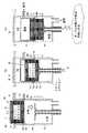
図2に、搬送体15の構造を示す。図2(A)は側部断面図であり、図2(B)は上部断面図である。
【0071】
搬送体15は、基板支持部16を備える。基板支持部16は、アルミ製であり、約3mmの厚みを有する。基板支持部16は、基板1を受けるため、基板の面内方向に6ヵ所が、なめらかな山型に突出している。突出部の先端近傍には、基板1に当接して基板1を支持する、テフロン樹脂からなる、ピン17が設けられている。基板1のサイズについて説明すると、厚みは1.1mmであり、幅は550mmであり、長さ650mmである。幅方向に、基板の端部から約150mm内側にピン17が設けられている。基板1の端部はローラ(図示せず)で押さえられ、反りが、おおよそ10mm以下に抑えられている。各基板1間の間隙は30mm程度である。カセット5内に、20枚の基板1が収容されている。
【0072】
図3を参照して、処理装置7への基板1の搬送受渡し法を説明する。
図3(a)を参照して、複数の基板1が搭載されたカセット5をカセット収容容器8に収めてなる搬送体15を、処理装置の扉4を開いて、搬出入室6に収める。
【0073】
図3(b)を参照して、扉4を閉めて、搬送体15の下方に、大気圧よりわずかに陽圧の、清浄なN2などの不活性ガスを充填し、大気と置換する。その後、わずかに底板13を下降させる。なお、このとき、カセット収容容器(本体)8の外の、上部および側部の大気がカセット収容容器(本体)8の内部に入り込まないように、カセット収容容器(本体)8の底部18は、搬出入室6内に設けられた側壁突出部19とOリング14などを介して、当接させる。
【0074】
その後、図3(c)を参照して、搬出入室6の上部および下部領域を同時に真空引き排気する。ゲートバルブ20を開いた後、カセット5を定位置に順次下降させる。次に、図示しない隣接のロードロック室内に設けられたロボットで、基板1を1枚ごと、処理室2内に搬入する。また、処理が完了した基板は、逆にカセット5に戻される。
【0075】
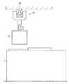
図4に、搬送体を搬送する搬送機の概略図を示す。天井22にレール23が配設されている。レール23に車24を取付けて、搬送機21が移動できるようになっている。搬送機21は、たとえば自走式で、各搬送機21は回転モータ(図示せず)を内蔵している。レール23の下部には、高周波等の電源と信号を供給する給電線管25が配設されている。高周波電流を流し、誘導電流を発生させて回転モータを駆動させてもよい。これにより、非接触で発塵が少なくなる。しかも、搬送機21内に大容量の充電器を設ける必要がなく、かつ充電時間ロスを発生させることなく、給電できる。
【0076】
また、搬送機21は、半導体15を引っかける抜差しピン26および搬送体15の受渡し時などに稼動する昇降ユニット27を備えている。
【0077】
また、図5に示すように、多数ある処理装置7の中、少なくとも一部の上に、搬送機21の通過経路または搬送体15の受渡し位置を配置するように、軌道レール23を配設する。床面にレール等を配設することがないので、工場全体の床面積を格段に小さくすることができる。また、床の作業者の作業性を改善することができ、かつ安全性を確保することができる。
【0078】
なお、本実施例では、搬出入室6の隣接室がロードロック室3の場合を例示したが、その他、ロボット室、前処理室、処理室等、各種従来同様の装置の基板の受入れまたは中継室であってもよい。
【0079】
今回開示された実施の形態はすべての点で例示であって制限的なものではないと考えられるべきである。本発明の範囲は上記した説明ではなくて特許請求の範囲によって示され、特許請求の範囲と均等の意味および範囲内でのすべての変更が含まれることが意図される。
【図面の簡単な説明】
【図1】 本発明の実施の形態に係る処理装置の部分断面図である。
【図2】 本発明の実施の形態に係る搬送体の構造を示す図である。
【図3】 処理装置への基板の搬送受渡し法を説明するための図である。
【図4】 本発明の実施の形態に係る搬送機の断面図である。
【図5】 本発明に係る搬送機を軌道レールに配設した状態を説明するための断面図である。
【図6】 従来の処理装置の概略断面図である。
【図7】 従来の処理装置の概略平面図である。
【図8】 従来のカセット収容容器用ポートの断面図である。
【図9】 従来のカセット水平移動機構の斜視図である。
【図10】 他の従来の処理装置を示す図である。
【図11】 さらに他の従来の処理装置の概略断面図である。
【符号の説明】
1 基板、2 処理室、3 ロードロック室、6 搬出入室、8 カセット収容容器、11 シャフト、13 底板。[0001]
BACKGROUND OF THE INVENTION
The present invention generally relates to an electronic component manufacturing apparatus, and more particularly, to an electronic component manufacturing apparatus suitable for use of a large substrate having a diameter of several hundred mm or several hundred mm square. The present invention also relates to a method for manufacturing an electronic component suitable for use of such a large substrate.
[0002]
[Prior art]
In general, in the manufacturing process of various electronic components such as semiconductors, liquid crystal display devices, and image sensors, a large number of products are manufactured simultaneously so that the components can be manufactured efficiently. In order to manufacture a large display device or the like, a large substrate is used. Various production technologies and processing devices have been developed and put into practical use every year or every day so that even larger substrate sizes can be manufactured with the aim of further increasing the number of components and increasing the size of parts.
[0003]
In addition, the manufacturing process of these electronic components usually has many processing steps, forming a thin film by a CVD method or a sputtering method on a substrate as an object to be processed, forming an impurity concentration region by a thermal diffusion method, various thin films. A large number of various processing apparatuses are used in the pattern formation.
[0004]
In these electronic parts, tens of thousands or more of fine patterns of the order of μm or less are formed, and as with the previous enlargement, further high definition has been pursued, and floating foreign objects that cannot be seen. And gas also cause defects in pattern formation and chemical reaction. For this reason, the entire process such as the processing apparatus, the inspection apparatus, and the transfer apparatus is housed in a clean room having a cleanness such as
[0005]
However, the construction cost of clean room facilities is extremely increased as the degree of cleanliness increases. Especially in factories that handle large substrates, especially in new factories, the flow of air changes complicatedly due to the arrangement of equipment and the movement of work in the process at startup, and measures to suppress the scattering of foreign substances and impurities at important points. In addition, it is difficult to manage and maintain cleanliness. Also, the factory startup period, construction and running costs are increasing. Also, as the number of check points for dust-proof measures for workers in the process, such as dust-proof clothing, increases, and the work in a wide process increases, the work environment of the worker himself is becoming worse.
[0006]
As a method for solving these problems, for example, processing apparatuses described in JP-A-6-196545, JP-A-7-161797, JP-A-7-297257, and the like have been proposed. In either case, a pot (or pod or cassette housing container) including a cassette containing a large number of substrates and a detachable cover is used for clean substrate transfer between processing apparatuses. In this way, improvements such as reducing the high clean area of the entire line can be achieved.
[0007]
The apparatus disclosed in Japanese Patent Laid-Open No. 7-161797 will be described with reference to FIGS.
[0008]
This apparatus includes a
[0009]
On the other hand, the carry-in / out
[0010]
The
[0011]
The
[0012]
As shown in FIG. 6, the container bottom portion mounting table 113 is attached to the tip of the
[0013]
Referring to FIG. 9, the
[0014]
A
[0015]
A
[0016]
A
[0017]
An
[0018]
The apparatus described in Japanese Patent Laid-Open No. 6-196545 includes a
[0019]
In the apparatus described in Japanese Patent Application Laid-Open No. 7-297257, the cassette C is integrated with the
[0020]
In the case of a liquid crystal display device supporting the substrate in the cassette with full support, there is a problem that scratches and dust generation occur. Therefore, there are many shapes in which an interval of about several tens of millimeters is provided between the bottom surfaces of two opposing substrates.
[0021]
[Problems to be solved by the invention]
Now, in the manufacturing process of various electronic components such as semiconductors and liquid crystal display devices, an increase in the size of the substrate is progressing. In addition, the number of processes and processing devices is large, and a large-scale factory facility is required. However, in order to reduce construction, maintenance, maintenance costs, etc., facilitate transportation from equipment manufacturers to factories by trucks, etc., and improve workability such as manufacturing and process management, each process or equipment to be moved or incidental It is necessary to reduce the size of equipment.
[0022]
Moreover, it is necessary to reduce the vacuuming time so as not to drop the production tact. In order to eliminate the need for complicated air conditioning such as adjusting three HEPAs and to stabilize the cleanliness as in JP-A-7-161797, a spare chamber for delivering a substrate to a load lock chamber or the like. It is necessary to make the volume as small as possible.
[0023]
However, in the apparatus described in Japanese Patent Application Laid-Open No. 7-161797 or Japanese Patent Application Laid-Open No. 7-297257, the space for the carry-in / out chamber needs to be 20 times or more larger than the volume of the outer periphery of the cassette on the X × Y plane in FIG. It becomes. Further, with reference to FIG. 7, when considering the depth direction B, a large space is required that is twice to three times or more.
[0024]
Therefore, the following items will be considered.
(1) A plurality of cassettes and cassette storage containers are stored in the loading / unloading chamber.
[0025]
(2) The transfer of the cassette and the cassette storage container and the lifting mechanism are stored in the carry-in / out chamber.
[0026]
(3) The elevating mechanism of the cassette or cassette container is stored in the carry-in / out chamber. And the raising / lowering mechanism should be formed in the side part of a cassette or a cassette storage container. Providing such an operation or sliding part in the carry-in / out chamber has problems such as the product quality and the yield being liable to decrease due to dust generation. In particular, in a liquid crystal display device, a large substrate of several hundred mm square or more is used, and the weight including a cassette is large. If a sliding portion is provided in such a cantilever structure, a large moment can be resisted. The
[0027]
(4) The apparatus disclosed in Japanese Patent Laid-Open No. 7-161797 requires a complicated air conditioner that adjusts the flow rate and position of three HEPAs in order to stabilize the cleanliness. It's hard.
[0028]
(5) In particular, in a liquid crystal display device, a large substrate of several hundred mm square or more is used, and the thickness is as thin as 0.5 to 1.1 mm. Warps about tens of mm. Therefore, it is necessary to increase the distance between the substrates in order to prevent interference and cracking during substrate delivery. However, the cassette and the cassette housing container are large and the weight is increased, and the above problems (1) to (3) are synergistically increased.
[0029]
In the apparatus described in Japanese Patent Laid-Open No. 6-196545, the problem (1) is reduced, but the problems (2) to (5) are also present. That is, as shown in FIG. 10, compared to the cassette size, a space about 10 times that of the cassette is required in the plane of the cross-sectional view shown in FIG.
[0030]
Furthermore, in the manufacturing process of these electronic components, an automated guided vehicle that moves on a rail laid on a floor surface is generally used for transporting a cassette on which a board is mounted. However, in this case, an automatic guided vehicle track rail, various processing devices, and a HEPA unit for improving cleanliness are installed on the floor surface. As a result, the floor area increases. As a result, the effective floor area ratio is lowered, maintenance and daily workability are deteriorated, the cleanliness management in the process becomes difficult, and the construction cost of the factory is increased.
[0031]
Therefore, an object of the present invention is to provide an electronic component manufacturing apparatus with an improved effective floor area.
[0032]
Another object of the present invention is to provide an electronic component manufacturing apparatus that does not deteriorate maintenance and daily workability.
[0033]
Still another object of the present invention is to provide an electronic component manufacturing apparatus that facilitates the cleanliness management in the process.
[0034]
Still another object of the present invention is to provide an improved part manufacturing apparatus that can reduce the construction cost of a factory.
[0035]
Still another object of the present invention is to provide a method of manufacturing an electronic component using such a manufacturing apparatus.
[0036]
[Means for Solving the Problems]
According to a first aspect of the present invention, there is provided an electronic component manufacturing apparatus including a processing chamber for performing predetermined processing on a substrate. An adjacent chamber such as a load lock chamber for performing an operation of transferring the substrate to the processing chamber is connected to the processing chamber. From the cassette in which a plurality of the above substrates are stacked in the adjacent chamber at intervals in the vertical direction, the substrate is taken out,Adjacent room A loading / unloading chamber for storing a cassette container for performing an operation for unloading is connected. The apparatus includes a transporter that moves on a rail track disposed on a ceiling, and that transports the cassette into a cassette storage container and transports the cassette to the carry-in / out chamber. Elevating means for elevating and lowering the cassette that has been transported together with the cassette container is provided in the carry-in / out chamber.The carry-in / out chamber has a door that is opened and closed when the cassette container is carried in, accommodates the cassette container, and with the door closed, is filled with an inert gas below the cassette container. It is evacuated after gas filling. Projection provided on the inner wall of the carry-in / out chamber, and cassette storage containerBottom of Provided in contact with the protrusionBy doing so, the loading / unloading chamber can be blocked into the upper area and the lower area An O-ring is provided. The apparatus includes unloading means for unloading only one substrate from the cassette in the horizontal direction at a substantially constant horizontal position and unloading the substrate to the adjacent chamber.
[0037]
According to the present invention, a single cassette (or a minimum number of about two or three in a horizontal orientation or the like for improving the processing duct) is stored in the loading / unloading chamber (or the processing tact is stored). In order to improve, the processing apparatus may be provided with a plurality of loading / unloading chambers).
[0038]
Further, there is no storage or transfer of a plurality of cassettes and cassette storage containers in the carry-in / out chamber, and a transfer mechanism or the like is not necessary. Further, since a part of the lifting mechanism is placed outside the carry-in / out chamber and the substrate is taken out at a certain horizontal position, the entrance to the adjacent chamber such as the adjacent load lock chamber can be made small.
[0039]
Therefore, in the substrate transfer manufacturing process in clean gas-sealed containers for various electronic components such as semiconductors and liquid crystal display devices, even if the substrate is large, the number of processes and the number of processing devices are much smaller. (Can be reduced to a fraction of the conventional one). Therefore, factory facilities can be minimized, construction, maintenance and maintenance costs can be suppressed, trucks can be easily transported from the manufacturer to the factory, and workability such as manufacturing and process management can be improved.
[0040]
In addition, manufacturing time can be suppressed by reducing the vacuuming time and the like. Further, as in JP-A-7-161797, complicated air conditioning adjustment for adjusting three HEPAs is not required. In addition, the cleanliness can be stabilized and the quality and yield of the product can be improved.
[0041]
Moreover, the floor area can be reduced without installing the rails for the carriage track on the floor. This increases the effective floor area ratio, improves maintenance and daily workability, facilitates the cleanliness management in the process, and reduces the construction cost of the factory.
[0042]
In the electronic component manufacturing apparatus according to
[0043]
According to this invention, the raising / lowering mechanism of a cassette or a cassette storage container is stored out of the carrying in / out chamber. And the raising / lowering mechanism is formed near the center of a cassette storage container. Therefore, it is possible to eliminate the deterioration of product quality and yield due to dust generation on the sliding portion, etc., to facilitate maintenance work, to reduce the strength of the screw portion and the shaft portion, and to reduce the size.
[0044]
In addition, since there is no lifting mechanism or the like on the side of the cassette container, the carry-in route of the cassette container can be made small, and the carry-in robot and transfer device are simple and easy to design. For example, an internal pressure gauge for confirmation or a viewing window for the substrate can be attached to the side of the cassette housing container, and the glass substrate can be easily broken and confirmed in the substrate loading process.
[0045]
Moreover, the floor area can be reduced without installing the rails for the carriage track on the floor. This increases the effective floor area ratio, improves maintenance and daily workability, facilitates the cleanliness management in the process, and reduces the construction cost of the factory.
[0046]
In the electronic component manufacturing apparatus according to a third aspect, the cassette includes substrate support means having at least four protrusions extending in the horizontal direction for supporting the substrate from below at least at four points. A pin that contacts the substrate from below and supports the substrate is provided at the tip of the protruding portion.
[0047]
Also in this invention, the plurality of cassette containers can be reduced in weight and size, and the carry-in / out chamber can also be reduced in size.
[0048]
In addition, in the two-dimensional ideal solution, in the two-point support of the substrate, the maximum deflection of the substrate is proportional to the cube of the distance between the supports and inversely proportional to the cube of the thickness of the substrate. The amount of warpage of the substrate increases extremely. By reducing the distance between the support points, the warpage is reduced, and defects such as chipping and cracking of the substrate caused by abnormal vibration such as when the substrate is delivered and slight positional displacement are reduced, and the substrate in the cassette By reducing the interval, the cassette container can be downsized.
[0049]
Line support in the vicinity of the two edges and support over a wide range of surfaces (for example, almost the entire surface) are not preferable because the contact portion with the substrate increases and the probability of foreign matter adhesion or damage increases. In addition, providing a wide range of support portions is not preferable because the weight of the entire cassette increases and it becomes difficult to receive the substrate. Therefore, it is preferable to provide approximately 4 to 6 convex protrusions.
[0050]
Moreover, the support part is preferably aluminum, which ensures rigidity, is relatively lightweight, and can be easily cleaned regularly. The contact portion of the substrate is preferably made of a resin such as Teflon that does not damage the substrate, has little wear and chipping, and has high chemical resistance against an acidic cleaning agent.
[0051]
Furthermore, the floor area can be reduced without installing the rails for the carriage track on the floor. This increases the effective floor area ratio, improves maintenance and daily workability, facilitates the cleanliness management in the process, and reduces the construction cost of the factory.
[0052]
In the electronic component manufacturing apparatus according to a fourth aspect, at least six protrusions are provided.
[0053]
In order to achieve a good balance between reducing warpage of a large rectangular substrate such as liquid crystal and reducing the weight of the cassette, the number of protrusions is preferably about six. In the two-dimensional ideal solution, the warpage can be reduced to about 1/8.
[0054]
In the electronic device manufacturing apparatus according to a fifth aspect of the present invention, the protruding portion has a planar shape and has a smooth curved mountain shape.
[0055]
In order to reduce the weight and rigidity of the substrate support, a cross-sectional shape of the substrate support that allows the stress to be uniform with respect to the cantilever support is preferable. In addition, it is preferable to make the thickness uniform so that the distance between the substrates is minimized and the processing and assembly of the plate material and the like are easy. Furthermore, a smooth mountain shape (wave shape) or the like is preferable in order to eliminate corners and the like to prevent scratches and dust generation when contacting the substrate.
[0056]
In the electronic component manufacturing apparatus according to a sixth aspect, the rail track and the carry-in / out chamber overlap in a plan view.
[0057]
According to this invention, the floor area can be reduced, the effective floor area ratio can be increased, the cleanliness management in the process can be facilitated, and the construction cost of the factory can be suppressed.
[0058]
In the electronic component manufacturing method according to
[0059]
According to the present invention, the same effect as described in the first aspect can be obtained. In the electronic component manufacturing method according to an eighth aspect of the present invention, the cassette housing container is transported with a positive pressure in the cassette housing container.
[0060]
The inside of the transport body may be at a vacuum pressure if it is a clean gas. However, due to breakage or the life of the O-ring, etc., the outside unclean air may not enter. For a series of workability such as opening and shortening the time, it is preferable to make the pressure slightly positive from the atmospheric pressure.
[0061]
In the electronic component manufacturing method according to the ninth aspect, the substrate is carried into the adjacent chamber by a transfer means provided in the adjacent chamber.
[0062]
According to the present invention, there is no need to newly provide a substrate carry-in device.
[0063]
DETAILED DESCRIPTION OF THE INVENTION
Embodiments of the present invention will be described below with reference to the drawings.
[0064]
FIG. 1 is a partial sectional view of an electronic component manufacturing apparatus according to the present invention.
Although the main body of the processing apparatus is omitted, any single or continuous processing such as thin film formation such as sputtering and CVD, inspection, resist coating, exposure, patterning such as patterning, heating, drying, cleaning ion implantation, etc. It can also be used for these devices.
[0065]
Referring to FIG. 1, a manufacturing apparatus according to the present invention includes a
[0066]
The
[0067]
However, n
[0068]
Further, a
[0069]
By introducing an inert gas having a high degree of cleanliness into a space surrounded by a cassette housing container (main body) 8 on which a plurality of
[0070]
FIG. 2 shows the structure of the
[0071]
The
[0072]
With reference to FIG. 3, a method for transferring the
Referring to FIG. 3A, a
[0073]
Referring to FIG. 3 (b), the
[0074]
Thereafter, referring to FIG. 3C, the upper and lower regions of the carry-in / out
[0075]
FIG. 4 shows a schematic diagram of a transporter that transports the transport body.
[0076]
Further, the
[0077]
In addition, as shown in FIG. 5, the track rails 23 are disposed so that the passing path of the
[0078]
In this embodiment, the
[0079]
The embodiment disclosed this time should be considered as illustrative in all points and not restrictive. The scope of the present invention is defined by the terms of the claims, rather than the description above, and is intended to include any modifications within the scope and meaning equivalent to the terms of the claims.
[Brief description of the drawings]
FIG. 1 is a partial cross-sectional view of a processing apparatus according to an embodiment of the present invention.
FIG. 2 is a diagram showing a structure of a transport body according to an embodiment of the present invention.
FIG. 3 is a diagram for explaining a method of transferring a substrate to a processing apparatus.
FIG. 4 is a cross-sectional view of a transporter according to an embodiment of the present invention.
FIG. 5 is a cross-sectional view for explaining a state in which the transporter according to the present invention is disposed on the track rail.
FIG. 6 is a schematic sectional view of a conventional processing apparatus.
FIG. 7 is a schematic plan view of a conventional processing apparatus.
FIG. 8 is a cross-sectional view of a conventional cassette housing container port.
FIG. 9 is a perspective view of a conventional cassette horizontal movement mechanism.
FIG. 10 is a diagram showing another conventional processing apparatus.
FIG. 11 is a schematic sectional view of still another conventional processing apparatus.
[Explanation of symbols]
1 substrate, 2 processing chamber, 3 load lock chamber, 6 carry-in / out chamber, 8 cassette container, 11 shaft, 13 bottom plate.
Claims (9)
Translated fromJapanese前記処理室に接続され、前記基板を前記処理室に移送する操作を行なうロードロック室等の隣接室と、
前記隣接室に接続され、前記基板を複数枚上下方向に間隔をおいて積み重ねて搭載したカセットの中から、該基板を取出して、前記隣接室へ搬出する操作を行ない、カセット収容容器を搬入する際に開閉される扉を有し、前記カセット収納容器を収容し、前記扉を閉めた状態で、前記カセット収納容器の下方に不活性ガスが充填され、該不活性ガス充填後に真空引きされる搬出入室と、
天井に配設されたレール軌道を移動し、前記カセットをカセット収容容器に入れて前記搬出入室へ搬送する搬送機と、
前記搬出入室内に設けられ、カセット収容容器とともに搬送されてきた前記カセットを昇降させる昇降手段と、
前記搬出入室の内壁に設けられた突出部と、
前記カセット収容容器の底部に設けられ、前記突出部と当接することにより、前記搬入出室を上部領域と下部領域とに遮断可能なOリングと、
前記カセットから、ほぼ一定の水平位置で水平方向に前記基板を1枚だけ取出して、前記隣接室へ搬出する搬出手段とを備えた、電子部品の製造装置。A processing chamber for performing predetermined processing on the substrate;
An adjacent chamber such as a load lock chamber that is connected to the processing chamber and performs an operation of transferring the substrate to the processing chamber;
The cassette is connected to the adjacent chamber, and a plurality of the substrates stacked in the vertical direction are stacked and mounted, and the substrate is taken out and transferred to the adjacent chamber, and the cassette container isloaded. In the state where the cassette storage container is accommodated and the door is closed, the cassette storage container is filled with an inert gas and is evacuated after the inert gas is filled. Carry-in / out rooms,
A transporter that moves on a rail track disposed on the ceiling, and that transports the cassette into a cassette storage container and transports it to the loading / unloading chamber;
Elevating means for elevating and lowering the cassette provided in the carry-in / out chamber and conveyed together with the cassette container,
A protrusion provided on the inner wall of the carry-in / out chamber;
An O-ring provided atthe bottom of the cassette containerand capable of blocking the carry-in / out chamber into an upper region and a lower region by abuttingagainst the protruding portion;
An electronic component manufacturing apparatus, comprising: an unloading means for unloading only one substrate from the cassette in a horizontal direction at a substantially constant horizontal position and unloading the substrate to the adjacent chamber.
前記カセットの重心近傍を下から支えて、該カセットを昇降させる昇降部と、
前記搬出入室の外部に設けられ、前記昇降部を受ける受け部と、を含み、
前記昇降部は、ベローズで囲まれている、請求項1に記載の電子部品の製造装置。The lifting means is
A lifting part for supporting the vicinity of the center of gravity of the cassette from below and raising and lowering the cassette,
A receiving part that is provided outside the carry-in / out chamber and receives the elevating part,
The electronic component manufacturing apparatus according to claim 1, wherein the elevating unit is surrounded by a bellows.
前記突出部の先端部には、前記基板に下から当接し、該基板を支持するピンが設けられている、請求項1に記載の電子部品の製造装置。The cassette comprises substrate support means having at least four protrusions extending horizontally, supporting the substrate from below at at least four points,
The electronic component manufacturing apparatus according to claim 1, wherein a pin that abuts the substrate from below and supports the substrate is provided at a tip portion of the projecting portion.
前記搬出入室の内壁に設けられた突出部と、前記カセット収容容器の底部に設けられたOリングとを当接させることにより前記搬出入室を上部領域と下部領域に遮断する工程と、
前記搬入出口を閉めて前記搬出入室内に前記カセット収容容器を位置させた状態で、前記搬出入室の前記下部領域の雰囲気を清浄な気体で置換する工程と、
前記カセット収容容器から前記カセットを取出し、これを前記下部領域まで下降させる工程と、
前記搬入出室内を真空引きする工程と、
前記カセットから、ほぼ一定の水平位置で水平方向に、前記基板を1枚だけ取出し、隣接室へ搬入する工程とを備えた、電子部品の製造方法。A step of transferring a cassette in which a plurality of substrates are stacked and spaced in the vertical direction by a transfer machine that moves on a rail track disposed on the ceiling into a cassette storage container andtransferring the cassettefrom aloading / unloading port to aloading / unloading chamber. When,
Shutting the carry-in / out chamber into an upper region and a lower region by bringing a protrusion provided on the inner wall of the carry-in / out chamber into contact with an O-ring provided atthe bottom of the cassette container;
A step of replacing the atmosphere in the lower region of theloading / unloading chamber with a clean gas in a state where theloading / unloading portis closed and the cassette container is positioned in theloading / unloading chamber;
Removing the cassette from the cassette container and lowering it to the lower region;
Evacuating the loading / unloading chamber;
From the cassette, horizontally at a substantially constant horizontal position, taken out only one of the substrate,and a step of loading into the adjacent chamber, a method of manufacturing an electronic component.
Priority Applications (1)
| Application Number | Priority Date | Filing Date | Title |
|---|---|---|---|
| JP26731599AJP3769425B2 (en) | 1999-09-21 | 1999-09-21 | Electronic component manufacturing apparatus and electronic component manufacturing method |
Applications Claiming Priority (1)
| Application Number | Priority Date | Filing Date | Title |
|---|---|---|---|
| JP26731599AJP3769425B2 (en) | 1999-09-21 | 1999-09-21 | Electronic component manufacturing apparatus and electronic component manufacturing method |
Publications (2)
| Publication Number | Publication Date |
|---|---|
| JP2001093957A JP2001093957A (en) | 2001-04-06 |
| JP3769425B2true JP3769425B2 (en) | 2006-04-26 |
Family
ID=17443122
Family Applications (1)
| Application Number | Title | Priority Date | Filing Date |
|---|---|---|---|
| JP26731599AExpired - Fee RelatedJP3769425B2 (en) | 1999-09-21 | 1999-09-21 | Electronic component manufacturing apparatus and electronic component manufacturing method |
Country Status (1)
| Country | Link |
|---|---|
| JP (1) | JP3769425B2 (en) |
Families Citing this family (9)
| Publication number | Priority date | Publication date | Assignee | Title |
|---|---|---|---|---|
| KR100882376B1 (en) | 2002-06-19 | 2009-02-05 | 브룩스 오토메이션, 인크. | Automatic material handling system for semiconductor manufacturing based on combination of vertical rotary storage lathe and overhead hoist |
| WO2004034438A2 (en) | 2002-10-11 | 2004-04-22 | Brooks Automation, Inc. | Access to one or more levels of material storage shelves by an overhead hoist transport vehicle from a single track position |
| JP4602359B2 (en)* | 2003-08-29 | 2010-12-22 | 株式会社日立プラントテクノロジー | Liquid crystal substrate transfer device |
| JP4494831B2 (en)* | 2004-03-11 | 2010-06-30 | 株式会社アルバック | Substrate transfer device and substrate transfer system provided with the same |
| JP2007115785A (en)* | 2005-10-18 | 2007-05-10 | Oki Electric Ind Co Ltd | Supporting container for thin plate |
| JP5277572B2 (en)* | 2007-06-26 | 2013-08-28 | 大日本印刷株式会社 | Plate-like material storage and transfer system and plate-like material storage and transfer method |
| JP7191678B2 (en)* | 2018-12-27 | 2022-12-19 | 株式会社アルバック | SUBSTRATE PROCESSING APPARATUS, CASSETTE REMOVAL METHOD OF SUBSTRATE PROCESSING APPARATUS |
| JP7224725B2 (en)* | 2019-03-26 | 2023-02-20 | 株式会社ディスコ | Conveyor system |
| KR102701743B1 (en)* | 2019-09-18 | 2024-08-30 | 무라다기카이가부시끼가이샤 | Return system and storage |
- 1999
- 1999-09-21JPJP26731599Apatent/JP3769425B2/ennot_activeExpired - Fee Related
Also Published As
| Publication number | Publication date |
|---|---|
| JP2001093957A (en) | 2001-04-06 |
Similar Documents
| Publication | Publication Date | Title |
|---|---|---|
| JP4581031B2 (en) | Substrate processing apparatus, substrate processing method, and semiconductor device manufacturing method | |
| KR100406337B1 (en) | Board Transfer and Processing System | |
| KR100221983B1 (en) | A treating apparatus for semiconductor process | |
| EP2092555B1 (en) | Workpiece stocker with circular configuration | |
| KR102033083B1 (en) | Semiconductor stocker systems and methods | |
| JP4977228B2 (en) | Substrate loading / unloading method and semiconductor device manufacturing method | |
| US11501987B2 (en) | Loadlock module and semiconductor manufacturing apparatus including the same | |
| US6120229A (en) | Substrate carrier as batchloader | |
| TWI868516B (en) | Conveying system, container opening and closing device | |
| KR20020019414A (en) | Substrate processing apparatus and method for manufacturing a semiconductor device by using the substrate processing apparatus | |
| JP2011517134A (en) | Clean transfer robot | |
| JP2002517055A (en) | Substrate handling and processing systems and methods | |
| JPH10256346A (en) | Cassette transferring mechanism and semiconductor manufacturing apparatus | |
| JP3769425B2 (en) | Electronic component manufacturing apparatus and electronic component manufacturing method | |
| JP3248129B2 (en) | Substrate transfer processing equipment | |
| JP3082389B2 (en) | Cleanroom storage | |
| KR19980071865A (en) | Substrate processing apparatus and method for repairing the same | |
| JP2002134588A (en) | Substrate conveying and processing apparatus | |
| JP4383636B2 (en) | Semiconductor manufacturing apparatus and semiconductor device manufacturing method | |
| JP2004303835A (en) | Substrate storing device | |
| KR100236272B1 (en) | Article storage cabinet for cleen room | |
| JP4155722B2 (en) | Substrate processing apparatus, pod opening / closing apparatus, substrate processing method, semiconductor device manufacturing method, and substrate transfer method | |
| JP3666636B2 (en) | Substrate processing equipment | |
| KR20200108467A (en) | Processing device, exhaust system, manufacturing method of semiconductor device | |
| KR102189275B1 (en) | Transfer robot and transfer apparatus including the same |
Legal Events
| Date | Code | Title | Description |
|---|---|---|---|
| A977 | Report on retrieval | Free format text:JAPANESE INTERMEDIATE CODE: A971007 Effective date:20050523 | |
| A131 | Notification of reasons for refusal | Free format text:JAPANESE INTERMEDIATE CODE: A131 Effective date:20050531 | |
| A521 | Written amendment | Free format text:JAPANESE INTERMEDIATE CODE: A523 Effective date:20050713 | |
| A131 | Notification of reasons for refusal | Free format text:JAPANESE INTERMEDIATE CODE: A131 Effective date:20051101 | |
| A521 | Written amendment | Free format text:JAPANESE INTERMEDIATE CODE: A523 Effective date:20051227 | |
| TRDD | Decision of grant or rejection written | ||
| A01 | Written decision to grant a patent or to grant a registration (utility model) | Free format text:JAPANESE INTERMEDIATE CODE: A01 Effective date:20060131 | |
| A61 | First payment of annual fees (during grant procedure) | Free format text:JAPANESE INTERMEDIATE CODE: A61 Effective date:20060206 | |
| R150 | Certificate of patent or registration of utility model | Free format text:JAPANESE INTERMEDIATE CODE: R150 | |
| FPAY | Renewal fee payment (event date is renewal date of database) | Free format text:PAYMENT UNTIL: 20090210 Year of fee payment:3 | |
| FPAY | Renewal fee payment (event date is renewal date of database) | Free format text:PAYMENT UNTIL: 20100210 Year of fee payment:4 | |
| FPAY | Renewal fee payment (event date is renewal date of database) | Free format text:PAYMENT UNTIL: 20110210 Year of fee payment:5 | |
| FPAY | Renewal fee payment (event date is renewal date of database) | Free format text:PAYMENT UNTIL: 20110210 Year of fee payment:5 | |
| FPAY | Renewal fee payment (event date is renewal date of database) | Free format text:PAYMENT UNTIL: 20120210 Year of fee payment:6 | |
| FPAY | Renewal fee payment (event date is renewal date of database) | Free format text:PAYMENT UNTIL: 20130210 Year of fee payment:7 | |
| LAPS | Cancellation because of no payment of annual fees |