JP3763378B2 - Light guide film manufacturing method, light guide film manufactured by the manufacturing method, laminated film, and liquid crystal display device - Google Patents
Light guide film manufacturing method, light guide film manufactured by the manufacturing method, laminated film, and liquid crystal display deviceDownload PDFInfo
- Publication number
- JP3763378B2 JP3763378B2JP20414198AJP20414198AJP3763378B2JP 3763378 B2JP3763378 B2JP 3763378B2JP 20414198 AJP20414198 AJP 20414198AJP 20414198 AJP20414198 AJP 20414198AJP 3763378 B2JP3763378 B2JP 3763378B2
- Authority
- JP
- Japan
- Prior art keywords
- light guide
- liquid crystal
- light
- guide film
- refractive index
- Prior art date
- Legal status (The legal status is an assumption and is not a legal conclusion. Google has not performed a legal analysis and makes no representation as to the accuracy of the status listed.)
- Expired - Fee Related
Links
Images


Landscapes
- Liquid Crystal (AREA)
- Laminated Bodies (AREA)
- Light Guides In General And Applications Therefor (AREA)
Description
Translated fromJapanese【0001】
【発明の属する技術分野】
本発明は、有機高分子からなる導光体フィルムの製造方法、その製造方法により製造された導光体フィルム、その導光体フィルムと偏光板または光拡散層とを積層した積層フィルム、およびこれらを液晶セルに装着した液晶表示装置に関するものである。
【0002】
【従来の技術】
従来、反射型カラー液晶表示装置は、液晶セルの外側に反射板を配置すると視差ずれを生じるため、液晶セル内に反射電極を形成する構成が提案されている。
【0003】
しかしながら、反射電極の端子が腐食されないようにするため、または効率的な拡散反射率を形成するため、反射電極の下地に工夫が要る等プロセスが複雑となり、良品率の低下を招くとともに高価になる問題点がある。
【0004】
そこで、視差ずれを防ぐとともに上記問題点を解決するために、液晶セルの外側の観察者とは反対側に鏡面反射板を装着するとともに液晶セルの観察者側の基板そのものを光ファイバープレートにする構成(特開平6−258627号公報)、または液晶セルの外側に光ファイバープレートを装着する構成(特開平6−59254号公報)が提案されている。
【0005】
一方、照明装置を備えた透過型液晶表示装置においては、光ファイバープレートを液晶セルとこの液晶セルを照明する照明装置との間等に装着する構成(特開平5−216031号公報)が提案されている。
【0006】
これら液晶表示装置に使用される光ファイバープレートは、GI(グレーデッドインデックス)型の石英系または樹脂系のもので、光ファイバー径が例えば0.5mmのものを最密構造となるように束ねてエポキシ樹脂または溶着等で固定し、これを光ファイバーの長さ方向に垂直な面で数mm以上の厚さで切断して両面を光学研磨している。
【0007】
【発明が解決しようとする課題】
前記従来技術では、視差ずれをなくすことができる、明るい反射型表示が実現できる、または高コントラストと広視野角との両立ができるが、太い光ファイバーを束ねているため、表示の解像度が低下する問題点がある。
【0008】
また、光ファイバープレートは、沢山の光ファイバーを束ねて切断するため、薄く製造すること、または液晶表示装置のような大面積のものを製造することが困難であるばかりでなく、製造できたとしても極めて高価なものになるという問題点がある。
【0009】
また、光ファイバープレートが石英系の場合には液晶表示装置が厚くて重く、樹脂系の場合には厚くなるという問題点を有する。さらに、石英系または樹脂系のどちらであっても厚くて硬いため、ローラーで液晶セルに貼り合わせて製造すること、または偏光板等の光学フィルムと積層一体化して同様に液晶セルに貼り合わせて製造することが困難であるという問題点がある。
【0010】
本発明は、以上のような従来の問題点に鑑みなされたものであって、貼り合わせまたは積層一体化が容易、大面積化が可能、解像度が高い、薄いおよび軽い導光体フィルムおよびその製造方法を提供することを目的としている。また、視差ずれがなく、明るい反射型表示が実現でき、高コントラストと広視野角との両立ができる安価で薄型軽量の液晶表示装置を提供することを目的としている。
【0011】
【課題を解決するための手段】
前述した目的を達成するために、本発明に係る導光体フィルムの製造方法は、屈折率の異なる2種以上の光重合性化合物からなる光重合性混合物層に、高圧水銀ランプからの光をフォトマスクを介して照射し、上記光重合性化合物を重合に伴って選択的に移動させて他の領域よりも屈折率の高い柱状構造を面内に複数個配列した後、上記水銀ランプからの光を全面に照射する方法としてもよい。
【0012】
本発明に係る導光体フィルムの製造方法は、屈折率の異なる2種以上の光重合性化合物からなる光重合性混合物層に、高圧水銀ランプからの光をフォトマスクを介して照射し、上記光重合性化合物を重合に伴って選択的に移動させて中心の屈折率が最も高く端部の屈折率が最も低くなるように連続的に屈折率が変化する柱状構造を面内に複数個配列した後、上記水銀ランプからの光を全面に照射する方法としてもよい。
【0013】
本発明に係る導光体フィルムの製造方法は、上記の製造方法において、上記フォトマスクはグラデーション加工が施されたマスクパターンを有している方法としてもよい。
【0014】
本発明に係る導光体フィルムの製造方法は、屈折率の異なる2種以上の光重合性化合物からなる光重合性混合物層上で光の干渉縞が交差するように光を上記光重合性混合物層に照射し、上記光重合性化合物を重合に伴って選択的に移動させて他の領域よりも屈折率の高い柱状構造を面内に複数個配列した後、紫外線を全面に照射することを特徴としている。
【0015】
本発明に係る導光体フィルムの製造方法は、屈折率の異なる2種以上の光重合性化合物からなる光重合性混合物層上で光の干渉縞が交差するように光を上記光重合性混合物層に照射し、上記光重合性化合物を重合に伴って選択的に移動させて中心の屈折率が最も高く端部の屈折率が最も低くなるように連続的に屈折率が変化する柱状構造を面内に複数個配列した後、紫外線を全面に照射することを特徴としている。
【0016】
本発明に係る導光体フィルムは、上記の製造方法により製造された導光体フィルムである。
【0017】
本発明に係る積層フィルムは、上記導光体フィルムと、偏光板とを積層してなることを特徴としている。
【0018】
本発明に係る積層フィルムは、上記導光体フィルムと、光拡散層とを積層してなることを特徴としている。
【0019】
本発明に係る液晶表示装置は、液晶セルの観察者側に、上記導光体フィルム、または上記積層フィルムを装着してなることを特徴としている。
【0020】
本発明に係る液晶表示装置は、液晶セルと該液晶セルを照明する照明装置との間に、上記導光体フィルム、または上記積層フィルムを装着してなることを特徴としている。
【0021】
本発明の製造方法によって製造された導光体フィルムによれば、微細な柱状構造が面内に複数個配列され、柱状構造はその他の領域よりも屈折率が高く形成され、厚さ方向に光を導く機能を有することにより、光ファイバープレートよりも大面積化が可能で、解像度が高く、薄くて軽いものを安価で得ることができる。また、柱状構造以外の領域を黒色等に着色しておけば、隣接する柱状構造の間隙からの光漏れを防ぐことができる。また、光ファイバープレートと違ってフレキシブルなため、偏光板または光拡散層との積層一体化を大面積でできるとともに、積層フィルムのカットを容易にできる。さらに、硬い液晶セル等への貼り合わせもローラー等で容易に行うことができる。
【0022】
また、微細な柱状構造が面内に近接状態で複数個配列され、柱状構造は、中心の屈折率が最も高く端部の屈折率が最も低くなるように、連続的に屈折率が変化するように形成され、厚さ方向に光を導く機能を有することにより、光ファイバープレートよりも大面積化が可能で、解像度が高く、薄くて軽いものを安価で得ることができる。また、光ファイバープレートと違ってフレキシブルなため、偏光板または光拡散層との積層一体化を大面積でできるとともに、積層フィルムのカットを容易にできる。さらに、硬い液晶セル等への貼り合わせもローラー等で容易に行うことができる。
【0023】
本発明の導光体フィルムの製造方法によれば、屈折率の異なる2種以上の光重合性化合物からなる光重合性混合物層に、高圧水銀ランプからの光を、フォトマスクを介して照射することによって、導光体フィルムを製造することにより、光重合性化合物の光重合速度の差を利用して、紫外線を照射した領域と照射しない領域とで屈折率の分布状態を異ならせ、微細な柱状構造を面内に複数個配列させることができる。しかも、光ファイバープレートよりも大面積化が可能で、解像度が高く、薄くて軽いものを安価で得ることができる。また、黒色等の着色性化合物を利用すれば、隣接する柱状構造の間隙からの光漏れを防ぐことができる。
【0024】
また、屈折率の異なる2種以上の光重合性化合物からなる光重合性混合物層に、高圧水銀ランプからの光を、フォトマスクのマスクパターンにグラデーション加工を施したものを介して照射することによって、導光体フィルムを製造することにより、光重合性化合物の光重合速度の差を利用して、紫外線の照射光量によって屈折率の分布状態を異ならせ、微細な柱状構造を面内に近接状態で複数個配列させることができる。しかも、光ファイバープレートよりも大面積化が可能で、解像度が高く、薄くて軽いものを安価で得ることができる。
【0025】
また、屈折率の異なる2種以上の光重合性化合物からなる光重合性混合物層に、前記光重合性混合物層上で光の干渉縞が交差するように光を照射することによって、導光体フィルムを製造することにより、光重合性化合物の光重合速度の差を利用して、紫外線を照射した領域と照射しない領域とで屈折率の分布状態を異ならせ、または紫外線の照射光量によって屈折率の分布状態を異ならせ、微細な柱状構造を面内に複数個配列させることができる。しかも、光ファイバープレートよりも大面積化が可能で、解像度が高く、薄くて軽いものを安価で得ることができる。また、黒色等の着色性化合物を利用すれば、隣接する柱状構造の間隙からの光漏れを防ぐことができる。
【0026】
本発明の積層フィルムによれば、上記製造方法により製造された導光体フィルムと偏光板とを積層してなることにより、光ファイバープレートと違ってフレキシブルなため、偏光板との積層一体化を大面積でできるとともに、積層フィルムのカットが容易にできる。さらに、硬い液晶セル等への貼り合わせもローラー等で容易に行うことができる。
【0027】
また、上記製造方法により製造された導光体フィルムと光拡散層とを積層してなることにより、光拡散層との積層一体化を大面積でできるとともに、積層フィルムのカットが容易にできる。さらに、硬い液晶セル等への貼り合わせもローラー等で容易に行うことができる。
【0028】
本発明の液晶表示装置によれば、液晶セルの観察者側に、上記製造方法により製造された導光体フィルム、または上記積層フィルムを装着してなることにより、光ファイバープレートを装着した場合に比べて液晶表示装置を薄型軽量とし、安価で得ることができる。特に、R、G、Bのカラーフィルターを利用したカラー液晶表示装置の場合には、隣接するカラーフィルターの混色がなく、色純度を高くすることができる。
【0029】
また、液晶セルと液晶セルを照明する照明装置との間に、上記製造方法により製造された導光体フィルム、または上記積層フィルムを装着してなることにより、光ファイバープレートを装着した場合に比べて液晶表示装置を薄型軽量とし、安価で得ることができる。特に、R、G、Bのカラーフィルターを利用したカラー液晶表示装置の場合には、隣接するカラーフィルターの混色がなく、色純度を高くすることができる。
【0030】
【発明の実施の形態】
図1乃至図9を用いて、本発明の実施の形態について説明する。尚、本発明は以下の実施の形態に限定されるものではない。
【0031】
(実施の形態1)
図1は本発明の一実施の形態である導光体フィルムの斜視図である。この導光体フィルム1は、高屈折率領域によって構成される微細な柱状構造2が面内に複数個配列されている構成である。図2は図1のX−X’線における断面図および屈折率nの分布状態、図3は柱状構造2の他の例を示す断面図および屈折率nの分布状態を示している。
【0032】
導光体フィルム1は、例えば以下のようにして作製することができる。
【0033】
まず、屈折率の異なる2種以上の光重合性化合物の組成物を調整する。光重合性化合物の組成物としては、例えば特開平9−127331号公報等に記載の光重合性組成物等を挙げることができる。それらの例としては、屈折率が異なる2種以上の光重合性二重結合を有するモノマーおよび/またはオリゴマーの組み合わせによる組成物が挙げられる。
【0034】
具体的な組み合わせとしては、2−ヒドロキシ−3−フェノキシプロピルアクリレート(屈折率1.526)を含むモノマーとポリエーテルウレタンアクリレート(屈折率1.460)、トリブロモフェノキシアクリレートを含むモノマーとポリエーテルウレタンアクリレート、フェノキシエチルアクリレートを含むモノマーとポリエーテルウレタンアクリレートを挙げることができる。光重合性化合物の組成物の中には、2−ヒドロキシ−2−メチルプロピオフェン等の光重合開始剤を使用することが好ましい。
【0035】
次に、この組成物を化学的および熱的に安定であるポリエチレンテレフタレートもしくはポリカーボネート等の高分子フィルムまたはガラス板からなる支持体基板の上に、公知の方法、例えばナイフコーター、ローラーコーター、スピンナー、ワイヤーバーコーター、ホワイラーまたはエクストルーダー等の方法を用いて塗布し、乾燥させて光重合性混合物層を設ける。必要に応じて、一対の支持体基板間に光重合性混合物層を配設してもよい。塗布膜厚としては1mm以下が好ましい。
【0036】
次に、光源に平行光が得られる紫外線用の高圧水銀ランプを使用し、波長400nm以下の紫外線をフォトマスクを介して前記光重合性混合物層に照射し、屈折率の異なる2種以上の光重合性化合物を重合に伴って選択的に移動させ、高屈折率領域樹脂部3として、断面が円形または四角形もしくは六角形等の多角形であって柱状径が100μm以下で高さが1mm以下の柱状構造2を、面内に複数個充填状態で形成する。その他の領域は、低屈折率樹脂部4となる。
【0037】
紫外線照射の際には、必要に応じて加温状態で行ってもよい。また、フォトマスクとしては、微細な円形または四角形もしくは六角形等の多角形が配列されたパターンが好ましい。このとき、必要に応じてパターンにグラデーションをかけておけば、図3に示すように、柱状構造2の中で屈折率が連続的に変化する屈折率傾斜領域樹脂部6と、屈折率傾斜領域樹脂部6同士の境界に位置する最低屈折率領域樹脂部5とを形成することができる。
【0038】
柱状構造2内の屈折率分布は、光重合性化合物の分子量、混合比、フォトマスクのパターン形状、紫外線の照射条件または加温条件等により、図2に示すような屈折率不連続型または図3に示すような屈折率傾斜型の柱状構造2を形成することができる。
【0039】
最後に、支持体基板全面に高圧水銀ランプを用いて紫外線を照射する。その後、支持体基板上に作製された導光体フィルム1を支持体基板より剥がし、大面積で薄くて軽い導光体フィルム1を得る。
【0040】
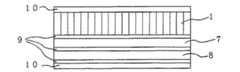
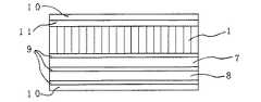
以下に、前述した導光体フィルム1を用いた積層フィルムについて、図4および図5を用いて説明する。
【0041】
本実施の形態の積層フィルムは、図4に示すように、吸収型偏光板7と位相差板8とを粘着剤層9を介して積層したものの表面に粘着剤層9を形成した後、前述した導光体フィルム1を重ねてローラーで加圧して積層一体化する。
【0042】
必要に応じて吸収型偏光板7の代わりに反射型偏光板を用いてもかまわない。また、位相差板8は必要に応じて粘着剤層9を介して複数枚重ねてもかまわない。
【0043】
最後に、位相差板8の表面に粘着剤層9を形成し、積層体の両表面に離型紙10を貼り合わせて積層フィルムを得る。尚、これら部材の積層順序は限定されるものでない。
【0044】
また、別の積層フィルムとして、図5に示すように、導光体フィルム1と離型紙10との間に光拡散層11を設けた積層フィルムを作製する。尚、これら部材の積層順序は限定されるものでない。
【0045】
光拡散層11の形成方法としては、透明樹脂にこの透明樹脂とは屈折率の異なるガラスビーズを混合したものを導光体フィルム1上に塗布し、光または熱によって硬化させる方法、または互いに屈折率の異なる樹脂を不均一に分散させた混合樹脂を塗布して硬化もしくはフィルム状態にしたものを粘着剤を介して貼り合わせる方法が適宜採用される。
【0046】
以下に、前述した積層フィルムを用いた反射型カラー液晶表示装置について、図6を用いて説明する。
【0047】
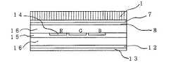
本実施の形態の反射型カラー液晶表示装置は、図6に示すように、図4に示す積層フィルムの位相差板8側の離型紙10を剥離して、液晶セルの電極基板16の観察者側に重ねてローラーで加圧し、積層フィルムを液晶セルに積層する。その後、導光体フィルム1側の離型紙10を剥離する。
【0048】
尚、液晶セルは、反射型STN構造で、液晶セルの内部には画素に対応させてR、G、Bのカラーフィルター14を形成し、液晶セルの観察者とは反対側には反射型偏光板12と鏡面反射板13とを配設している。一対の電極基板16間には液晶15が封入されている。
【0049】
このようすれば、視差ずれによってR、G、Bの各隣接画素間で色が混合することがなく、明るく高コントラストの反射型カラー表示を実現できる。
【0050】
以下に、前述した積層フィルムを用いた透過型カラー液晶表示装置について、図7を用いて説明する。
【0051】
本実施の形態の透過型カラー液晶表示装置は、図7に示すように、図5に示す積層フィルムの位相差板8側の離型紙10を剥離して、液晶セルの電極基板16の観察者とは反対側、つまり照明装置側に重ねてローラーで加圧し、光拡散層11を有する積層フィルムを液晶セルに積層する。その後、光拡散層11側の離型紙10を剥離する。
【0052】
尚、液晶セルは、反射型STN構造で、液晶セルの内部には画素に対応させてR、G、Bのカラーフィルター14を形成し、液晶セルの観察者側には位相差板8と吸収型偏光板7とを配設している。一対の電極基板16間には液晶15が封入されている。
【0053】
このようにすれば、冷陰極管からなる光源18とクサビ型の導光板プラスチック17等を備えたエッジライト型照明装置からの光を均一に拡散するとともに、導光体フィルム1を介して有効に液晶セルに導くことができ、高輝度化を実現することができる。
【0054】
(実施の形態2)導光体フィルムの作製における紫外線照射以外の方法については、実施の形態1と同様に行う。紫外線照射の方法は、特開平6−281805号公報に開示されている方法を応用して行う。
【0055】
支持体基板上に実施の形態1と同様に光重合性混合物層を配設する。この支持体基板に、直線偏光成分を含むコヒーレント光源であるエキシマレーザー等を使用し、支持体基板表面に散乱したコヒーレント光と支持体基板に入射してくるコヒーレント光との間での第1の干渉縞19をまずひとつの方向に照射する。
【0056】
次に、図8に示すように、第1の干渉縞19の照射方向に対して90度方向を変えて、同様に第2の干渉縞20を照射する。また、図9に示すように、第1の干渉縞19の照射方向に対して60度および120度方向を変えて、同様に第2の干渉縞20および第3の干渉縞21を照射する。
【0057】
この操作を繰り返して、屈折率が異なる2種以上の光重合性化合物を特定方向に選択移動させ、屈折率の分布を生じさせ、高屈折率領域樹脂部3と低屈折率領域樹脂部4とを形成し、高屈折率領域樹脂部3として、断面が四角形または三角形の柱状構造を面内に複数個充填状態で形成する。柱状構造内の屈折率分布は、実施の形態1と同様に、図3に示すような屈折率傾斜型または図2に示すような屈折率不連続型のどちらでもよい。
【0058】
最後に、支持体基板全面に高圧水銀ランプを用いて紫外線を照射する。その後、支持体基板上に作製された導光体フィルムを支持体基板より剥がし、大面積で薄くて軽い導光体フィルムを得る。
【0059】
【発明の効果】
以上の説明のように、本発明の製造方法により製造された導光体フィルムによれば、微細な柱状構造が面内に複数個配列され、柱状構造はその他の領域よりも屈折率が高く形成され、厚さ方向に光を導く機能を有することにより、光ファイバープレートよりも大面積化が可能で、解像度が高く、薄くて軽いものを安価で得ることができる。また、硬い液晶セル等への貼り合わせもローラー等で容易に行うことができる。
【0060】
また、微細な柱状構造が面内に近接状態で複数個配列され、柱状構造は、中心の屈折率が最も高く端部の屈折率が最も低くなるように、連続的に屈折率が変化するように形成され、厚さ方向に光を導く機能を有することにより、光ファイバープレートよりも大面積化が可能で、解像度が高く、薄くて軽いものを安価で得ることができる。また、硬い液晶セル等への貼り合わせもローラー等で容易に行うことができる。
【0061】
本発明の導光体フィルムの製造方法によれば、屈折率の異なる2種以上の光重合性化合物からなる光重合性混合物層に、高圧水銀ランプからの光をフォトマスクを介して照射することによって、導光体フィルムを製造することにより、屈折率の分布状態を異ならせて微細な柱状構造を面内に複数個配列させることができる。しかも、光ファイバープレートよりも大面積化が可能で、解像度が高く、薄くて軽いものを安価で得ることができる。
【0062】
また、屈折率の異なる2種以上の光重合性化合物からなる光重合性混合物層に、高圧水銀ランプからの光を、フォトマスクのマスクパターンにグラデーション加工を施したものを介して照射することによって、導光体フィルムを製造することにより、屈折率の分布状態を異ならせて微細な柱状構造を面内に近接状態で複数個配列させることができる。しかも、光ファイバープレートよりも大面積化が可能で、解像度が高く、薄くて軽いものを安価で得ることができる。
【0063】
また、屈折率の異なる2種以上の光重合性化合物からなる光重合性混合物層に、前記光重合性混合物層上で光の干渉縞が交差するように光を照射することによって、導光体フィルムを製造することにより、屈折率の分布状態を異ならせて微細な柱状構造を面内に複数個配列させることができる。しかも、光ファイバープレートよりも大面積化が可能で、解像度が高く、薄くて軽いものを安価で得ることができる。
【0064】
本発明の積層フィルムによれば、上記製造方法によって製造された導光体フィルムと偏光板とを積層してなることにより、光ファイバープレートと違ってフレキシブルなため、偏光板との積層一体化を大面積でできるとともに、積層フィルムのカットが容易にできる。さらに、硬い液晶セル等への貼り合わせもローラー等で容易に行うことができる。
【0065】
また、上記製造方法によって製造された導光体フィルムと光拡散層とを積層してなることにより、光拡散層との積層一体化を大面積でできるとともに、積層フィルムのカットが容易にできる。さらに、硬い液晶セル等への貼り合わせもローラー等で容易に行うことができる。
【0066】
本発明の液晶表示装置によれば、液晶セルの観察者側に、上記製造方法によって製造された導光体フィルム、または上記積層フィルムを装着してなることにより、光ファイバープレートを装着した場合に比べて液晶表示装置を薄型軽量とし、安価で得ることができる。特に、R、G、Bのカラーフィルターを利用したカラー液晶表示装置の場合には、隣接するカラーフィルターの混色がなく、色純度を高くすることができる。
【0067】
また、液晶セルと液晶セルを照明する照明装置との間に、上記製造方法によって製造された導光体フィルム、または上記積層フィルムを装着してなることにより、光ファイバープレートを装着した場合に比べて液晶表示装置を薄型軽量とし、安価で得ることができる。特に、R、G、Bのカラーフィルターを利用したカラー液晶表示装置の場合には、隣接するカラーフィルターの混色がなく、色純度を高くすることができる。また、照明装置からの光を効率よく伝達できるため、高輝度化または低消費電力化を実現することができる。
【0068】
以上のように説明したが、上記導光体フィルムは、ファイバープレート機能を有するため、前述した液晶表示装置だけでなく、各種表示装置のフロント面、複数枚の液晶セル間の画像電送または広告表示等の各種用途に利用することができる。
【図面の簡単な説明】
【図1】 実施の形態に係る導光体フィルムを示す斜視図である。
【図2】 図1のX−X’線における断面図およびその屈折率分布状態を示す説明図である。
【図3】 柱状構造の他の例を示す断面図およびその屈折率分布状態を示す説明図である。
【図4】 実施の形態に係る積層フィルムを示す断面図である。
【図5】 実施の形態に係る他の積層フィルムを示す断面図である。
【図6】 実施の形態に係る反射型カラー液晶表示装置を示す断面図である。
【図7】 実施の形態に係る透過型カラー液晶表示装置を示す断面図である。
【図8】 実施の形態2に係る導光体フィルムの製造方法を示す説明図である。
【図9】 実施の形態2に係る他の導光体フィルムの製造方法を示す説明図である。
【符号の説明】
1 導光体フィルム
2 柱状構造
3 高屈折率領域樹脂部
4 低屈折率領域樹脂部
5 最低屈折率領域樹脂部
6 屈折率傾斜領域樹脂部
7 吸収型偏光板
8 位相差板
9 粘着剤層
10 離型紙
11 光拡散層
12 反射型偏光板
13 鏡面反射板
14 カラーフィルター
15 液晶
16 電極基板
17 導光板プラスチック
18 光源
19 第1の干渉縞
20 第2の干渉縞
21 第3の干渉縞[0001]
BACKGROUND OF THE INVENTION
The present invention relates to a method for producing a light guide film comprising an organic polymer, a light guide film produced by the production method, a laminated film in which the light guide film and a polarizing plate or a light diffusion layer are laminated, and these The present invention relates to a liquid crystal display device mounted on a liquid crystal cell.
[0002]
[Prior art]
2. Description of the Related Art Conventionally, a reflection type color liquid crystal display device has a configuration in which a reflection electrode is formed in a liquid crystal cell because a parallax shift occurs when a reflection plate is disposed outside the liquid crystal cell.
[0003]
However, in order to prevent the terminals of the reflective electrode from being corroded or to form an efficient diffuse reflectance, a process such as requiring a device for the base of the reflective electrode becomes complicated, leading to a decrease in the yield rate and high cost. There is a problem.
[0004]
Therefore, in order to prevent the parallax shift and solve the above problems, a configuration in which a specular reflector is mounted on the side opposite to the viewer outside the liquid crystal cell and the substrate on the viewer side of the liquid crystal cell itself is an optical fiber plate. (Japanese Patent Laid-Open No. 6-258627) or a configuration in which an optical fiber plate is mounted outside the liquid crystal cell (Japanese Patent Laid-Open No. 6-59254) has been proposed.
[0005]
On the other hand, in a transmissive liquid crystal display device including an illuminating device, a configuration (Japanese Patent Laid-Open No. 5-216031) is proposed in which an optical fiber plate is mounted between a liquid crystal cell and an illuminating device that illuminates the liquid crystal cell. Yes.
[0006]
The optical fiber plate used in these liquid crystal display devices is a GI (graded index) type quartz or resin type, and an optical fiber having an optical fiber diameter of, for example, 0.5 mm is bundled so as to have a close-packed structure and epoxy resin. Or it fixes by welding etc., this is cut | disconnected by the thickness of several mm or more in the surface perpendicular | vertical to the length direction of an optical fiber, and both surfaces are optically polished.
[0007]
[Problems to be solved by the invention]
In the prior art, the parallax shift can be eliminated, a bright reflective display can be realized, or high contrast and a wide viewing angle can be achieved at the same time, but because the thick optical fibers are bundled, the display resolution is reduced. There is a point.
[0008]
In addition, since the optical fiber plate bundles and cuts many optical fibers, it is difficult not only to manufacture thinly, or to manufacture a large area such as a liquid crystal display device. There is a problem that it becomes expensive.
[0009]
In addition, the liquid crystal display device is thick and heavy when the optical fiber plate is made of quartz, and thick when the optical fiber plate is made of resin. Furthermore, since it is thick and hard, whether it is quartz or resin, it can be manufactured by laminating it to a liquid crystal cell with a roller, or laminated and integrated with an optical film such as a polarizing plate, and similarly laminated to a liquid crystal cell. There is a problem that it is difficult to manufacture.
[0010]
The present invention has been made in view of the conventional problems as described above, and is easy to bond or laminate, can have a large area, has a high resolution, a thin and light light guide film, and its manufacture It aims to provide a method. It is another object of the present invention to provide an inexpensive, thin and light liquid crystal display device which can realize a bright reflective display without parallax shift and can achieve both high contrast and a wide viewing angle.
[0011]
[Means for Solving the Problems]
To achieve the above object, a manufacturing method of the light guide filmaccording to the present invention, the photopolymerizable mixture layer of two or more photopolymerizable compounds having different refractive indices, the light from a high pressure mercury lamp Irradiation through a photomask, the photopolymerizable compound is selectively moved along with the polymerization, and a plurality of columnar structures having a higher refractive index than other regions are arranged in a plane, and then from the mercury lamp. Amethod of irradiating the entire surface with lightmay be used.
[0012]
In the method for producing a light guide film accordingto the present invention, a photopolymerizable mixture layer composed of two or more photopolymerizable compounds having different refractive indexes is irradiated with light from a high-pressure mercury lamp through a photomask, A plurality of columnar structures in which the refractive index continuously changes so that the refractive index at the center is the highest and the refractive index at the end is the lowest by selectively moving the photopolymerizable compound during polymerization After that, the entire surfacemay be irradiated with light from the mercury lamp.
[0013]
The manufacturing method of the light guide film accordingto the present invention may be a method in which, in theabove manufacturing method, the photomask has a mask pattern subjected to gradation processing.
[0014]
The method for producing a light guide film accordingto the present invention comprises the step of producing a photopolymerizable mixture in which light interference fringes intersect on a photopolymerizable mixture layer composed of two or more photopolymerizable compounds having different refractive indexes. Irradiating the entire surface with a plurality of columnar structures having a higher refractive index than other regions by irradiating the layer and selectively moving the photopolymerizable compound along with the polymerization. It is a feature.
[0015]
The method for producing a light guide film accordingto the present invention comprises the step of producing a photopolymerizable mixture in which light interference fringes intersect on a photopolymerizable mixture layer composed of two or more photopolymerizable compounds having different refractive indexes. A columnar structure in which the refractive index continuously changes so that the refractive index at the center is the highest and the refractive index at the end is the lowest by irradiating the layer and selectively moving the photopolymerizable compound with polymerization. It is characterized by irradiating the entire surface with ultraviolet rays after being arranged in a plane.
[0016]
The light guide filmwhich concerns on this invention is a light guide film manufactured bysaid manufacturing method.
[0017]
Laminated filmaccording to the present invention is characterized in that formed by laminating theaforementioned light guide film, and a polarizing plate.
[0018]
Laminated filmaccording to the present invention is characterized in that formed by laminating theaforementioned light guide film, a light diffusion layer.
[0019]
The liquid crystal display deviceaccording to the present invention, on the viewer side of the liquid crystal cell is characterized by comprisingthe light guide film orthe laminated film was mounted.
[0020]
The liquid crystal display deviceaccording to the present invention, between the illumination device for illuminating the liquid crystal cell and the liquid crystal cell is characterized by comprisingthe light guide film orthe laminated film was mounted.
[0021]
According to the light guide film manufactured by the manufacturing method of the present invention, a plurality of fine columnar structures are arranged in a plane, the columnar structures are formed with a higher refractive index than the other regions, and light is emitted in the thickness direction. By having the function of guiding, it is possible to increase the area as compared with the optical fiber plate, and it is possible to obtain a thin, light material with high resolution at low cost. Further, if the region other than the columnar structure is colored black or the like, light leakage from the gap between adjacent columnar structures can be prevented. Moreover, since it is flexible unlike an optical fiber plate, lamination | stacking integration with a polarizing plate or a light-diffusion layer can be made in a large area, and the cut of a laminated | multilayer film can be made easy. Furthermore, the bonding to a hard liquid crystal cell or the like can be easily performed with a roller or the like.
[0022]
Also, a plurality of fine columnar structures are arranged in close proximity to each other in the plane, and the columnar structure continuously changes its refractive index so that the refractive index at the center is the highest and the refractive index at the end is the lowest. And having a function of guiding light in the thickness direction, it is possible to increase the area as compared with the optical fiber plate, and it is possible to obtain a thin, light material with high resolution at low cost. Moreover, since it is flexible unlike an optical fiber plate, lamination | stacking integration with a polarizing plate or a light-diffusion layer can be made in a large area, and the cut of a laminated | multilayer film can be made easy. Furthermore, the bonding to a hard liquid crystal cell or the like can be easily performed with a roller or the like.
[0023]
According to the method for producing a light guide film of the present invention, light from a high-pressure mercury lamp is irradiated through a photomask onto a photopolymerizable mixture layer made of two or more photopolymerizable compounds having different refractive indexes. Thus, by producing the light guide film, the difference in the refractive index distribution state is different between the region irradiated with ultraviolet rays and the region not irradiated using the difference in the photopolymerization rate of the photopolymerizable compound. A plurality of columnar structures can be arranged in the plane. In addition, the area can be made larger than that of the optical fiber plate, and a high resolution, thin and light material can be obtained at a low cost. Moreover, if a coloring compound such as black is used, light leakage from the gaps between adjacent columnar structures can be prevented.
[0024]
In addition, by irradiating the photopolymerizable mixture layer composed of two or more kinds of photopolymerizable compounds having different refractive indexes with light from a high-pressure mercury lamp through a mask pattern of a photomask subjected to gradation processing By manufacturing the light guide film, utilizing the difference in the photopolymerization rate of the photopolymerizable compound, the refractive index distribution state varies depending on the amount of ultraviolet light irradiation, and the fine columnar structure is in close proximity to the surface. A plurality can be arranged by. In addition, the area can be made larger than that of the optical fiber plate, and a high resolution, thin and light material can be obtained at a low cost.
[0025]
Further, by irradiating the photopolymerizable mixture layer composed of two or more kinds of photopolymerizable compounds having different refractive indexes so that the light interference fringes intersect on the photopolymerizable mixture layer, the light guide By making use of the difference in the photopolymerization rate of the photopolymerizable compound by producing a film, the refractive index distribution is different between the region irradiated with ultraviolet rays and the region not irradiated with ultraviolet rays, or the refractive index depends on the amount of ultraviolet irradiation light. It is possible to arrange a plurality of fine columnar structures in the plane by differentiating the distribution state. In addition, the area can be made larger than that of the optical fiber plate, and a high resolution, thin and light material can be obtained at a low cost. Moreover, if a coloring compound such as black is used, light leakage from the gaps between adjacent columnar structures can be prevented.
[0026]
According to the laminated film of the present invention, by laminating the light guide film produced by the above production method and the polarizing plate, it is flexible unlike the optical fiber plate. The area can be reduced and the laminated film can be easily cut. Furthermore, the bonding to a hard liquid crystal cell or the like can be easily performed with a roller or the like.
[0027]
Moreover, by laminating the light guide film produced by the above production method and the light diffusing layer, the laminated integration with the light diffusing layer can be performed in a large area, and the laminated film can be easily cut. Furthermore, the bonding to a hard liquid crystal cell or the like can be easily performed with a roller or the like.
[0028]
According to the liquid crystal display device of the present invention, on the viewer side of the liquid crystal cell, the manufacturing method lightguide films produced by or by formed by attachingthe laminated film, as compared with the case where the optical fiber plate is mounted Thus, the liquid crystal display device can be made thin and light and inexpensive. In particular, in the case of a color liquid crystal display device using R, G, and B color filters, there is no color mixing of adjacent color filters, and color purity can be increased.
[0029]
Also, by mounting the light guide film manufactured by the above manufacturing method or theabove laminated film between the liquid crystal cell and the lighting device that illuminates the liquid crystal cell, compared to the case where the optical fiber plate is mounted. The liquid crystal display device can be made thin and light and inexpensive. In particular, in the case of a color liquid crystal display device using R, G, and B color filters, there is no color mixing of adjacent color filters, and color purity can be increased.
[0030]
DETAILED DESCRIPTION OF THE INVENTION
An embodiment of the present invention will be described with reference to FIGS. The present invention is not limited to the following embodiment.
[0031]
(Embodiment 1)
FIG. 1 is a perspective view of a light guide film according to an embodiment of the present invention. The
[0032]
The
[0033]
First, a composition of two or more photopolymerizable compounds having different refractive indexes is prepared. As a composition of a photopolymerizable compound, the photopolymerizable composition etc. which are described in Unexamined-Japanese-Patent No. 9-127331 etc. can be mentioned, for example. Examples thereof include a composition comprising a combination of monomers and / or oligomers having two or more photopolymerizable double bonds having different refractive indexes.
[0034]
As a specific combination, a monomer containing 2-hydroxy-3-phenoxypropyl acrylate (refractive index 1.526) and a polyether urethane acrylate (refractive index 1.460), a monomer containing tribromophenoxy acrylate and a polyether urethane Mention may be made of monomers containing acrylates, phenoxyethyl acrylates and polyether urethane acrylates. In the composition of the photopolymerizable compound, it is preferable to use a photopolymerization initiator such as 2-hydroxy-2-methylpropiophene.
[0035]
Next, the composition is applied on a support substrate made of a polymer film or glass plate such as polyethylene terephthalate or polycarbonate that is chemically and thermally stable, by a known method such as a knife coater, a roller coater, a spinner, It coat | covers using methods, such as a wire bar coater, a wheeler, or an extruder, It dries and provides a photopolymerizable mixture layer. If necessary, a photopolymerizable mixture layer may be provided between the pair of support substrates. The coating film thickness is preferably 1 mm or less.
[0036]
Next, using a high-pressure mercury lamp for ultraviolet rays that can obtain parallel light as a light source, the photopolymerizable mixture layer is irradiated with ultraviolet rays having a wavelength of 400 nm or less through a photomask, and two or more kinds of light having different refractive indexes are irradiated. The polymerizable compound is selectively moved along with the polymerization, and the high refractive index
[0037]
The ultraviolet irradiation may be performed in a heated state as necessary. In addition, the photomask is preferably a pattern in which fine circles or polygons such as squares or hexagons are arranged. At this time, if gradation is applied to the pattern as necessary, as shown in FIG. 3, the refractive index gradient
[0038]
Depending on the molecular weight of the photopolymerizable compound, the mixing ratio, the pattern shape of the photomask, the irradiation condition of ultraviolet rays or the heating condition, etc., the refractive index distribution in the
[0039]
Finally, the entire surface of the support substrate is irradiated with ultraviolet rays using a high-pressure mercury lamp. Thereafter, the
[0040]
Below, the laminated | multilayer film using the
[0041]
As shown in FIG. 4, the laminated film of the present embodiment is formed by forming the pressure-
[0042]
If necessary, a reflective polarizing plate may be used instead of the absorbing
[0043]
Finally, the pressure-
[0044]
Moreover, as another laminated film, as shown in FIG. 5, a laminated film in which a
[0045]
The
[0046]
Hereinafter, a reflective color liquid crystal display device using the above-described laminated film will be described with reference to FIG.
[0047]
As shown in FIG. 6, the reflective color liquid crystal display device of the present embodiment peels off the
[0048]
The liquid crystal cell has a reflective STN structure, and R, G, and B color filters 14 are formed in the liquid crystal cell corresponding to the pixels, and the reflective polarization is provided on the opposite side of the liquid crystal cell from the viewer. A plate 12 and a specular reflector 13 are provided. A liquid crystal 15 is sealed between the pair of
[0049]
In this way, it is possible to realize a bright and high-contrast reflective color display without color mixing between adjacent pixels of R, G, and B due to a parallax shift.
[0050]
Hereinafter, a transmissive color liquid crystal display device using the above-described laminated film will be described with reference to FIG.
[0051]
As shown in FIG. 7, the transmissive color liquid crystal display device according to the present embodiment peels the
[0052]
The liquid crystal cell has a reflective STN structure, and R, G, and B color filters 14 are formed in the liquid crystal cell corresponding to the pixels, and the
[0053]
In this way, the light from the edge light type illumination device provided with the
[0054]
(Embodiment 2) The methods other than ultraviolet irradiation in the production of a light guide film are performed in the same manner as in
[0055]
A photopolymerizable mixture layer is disposed on the support substrate in the same manner as in the first embodiment. An excimer laser, which is a coherent light source including a linearly polarized light component, is used for the support substrate, and the first between the coherent light scattered on the support substrate surface and the coherent light incident on the support substrate is used. First, the
[0056]
Next, as shown in FIG. 8, the
[0057]
By repeating this operation, two or more kinds of photopolymerizable compounds having different refractive indexes are selectively moved in a specific direction to generate a refractive index distribution, and the high refractive index
[0058]
Finally, the entire surface of the support substrate is irradiated with ultraviolet rays using a high-pressure mercury lamp. Thereafter, the light guide film produced on the support substrate is peeled off from the support substrate to obtain a light light guide film having a large area and being thin and light.
[0059]
【The invention's effect】
As described above, according to the light guide film manufactured by the manufacturing method of the present invention, a plurality of fine columnar structures are arranged in a plane, and the columnar structures are formed with a higher refractive index than other regions. In addition, by having the function of guiding light in the thickness direction, it is possible to increase the area as compared with the optical fiber plate, and it is possible to obtain a thin, light material with high resolution at low cost. In addition, bonding to a hard liquid crystal cell or the like can be easily performed with a roller or the like.
[0060]
Also, a plurality of fine columnar structures are arranged in close proximity to each other in the plane, and the columnar structure continuously changes its refractive index so that the refractive index at the center is the highest and the refractive index at the end is the lowest. And having a function of guiding light in the thickness direction, it is possible to increase the area as compared with the optical fiber plate, and it is possible to obtain a thin, light material with high resolution at low cost. In addition, bonding to a hard liquid crystal cell or the like can be easily performed with a roller or the like.
[0061]
According to the method for producing a light guide film of the present invention, light from a high-pressure mercury lamp is irradiated through a photomask onto a photopolymerizable mixture layer composed of two or more photopolymerizable compounds having different refractive indexes. By manufacturing a light guide film, a plurality of fine columnar structures can be arranged in a plane with different refractive index distribution states. In addition, the area can be made larger than that of the optical fiber plate, and a high resolution, thin and light material can be obtained at a low cost.
[0062]
In addition, by irradiating the photopolymerizable mixture layer composed of two or more kinds of photopolymerizable compounds having different refractive indexes with light from a high-pressure mercury lamp through a mask pattern of a photomask subjected to gradation processing By manufacturing the light guide film, a plurality of fine columnar structures can be arranged in the vicinity in the plane by changing the refractive index distribution state. In addition, the area can be made larger than that of the optical fiber plate, and a high resolution, thin and light material can be obtained at a low cost.
[0063]
Further, by irradiating the photopolymerizable mixture layer composed of two or more kinds of photopolymerizable compounds having different refractive indexes so that the light interference fringes intersect on the photopolymerizable mixture layer, the light guide By producing a film, a plurality of fine columnar structures can be arranged in a plane by changing the refractive index distribution. In addition, the area can be made larger than that of the optical fiber plate, and a high resolution, thin and light material can be obtained at a low cost.
[0064]
According to the laminated film of the present invention, by laminating the light guide film produced by the above production method and the polarizing plate, it is flexible unlike the optical fiber plate. The area can be reduced and the laminated film can be easily cut. Furthermore, the bonding to a hard liquid crystal cell or the like can be easily performed with a roller or the like.
[0065]
Moreover, by laminating the light guide film produced by the above production method and the light diffusion layer, the lamination integration with the light diffusion layer can be performed in a large area, and the laminated film can be easily cut. Furthermore, the bonding to a hard liquid crystal cell or the like can be easily performed with a roller or the like.
[0066]
According to the liquid crystal display device of the present invention, on the viewer side of the liquid crystal cell, the manufacturing method lightguide films produced by or by formed by attachingthe laminated film, as compared with the case where the optical fiber plate is mounted Thus, the liquid crystal display device can be made thin and light and inexpensive. In particular, in the case of a color liquid crystal display device using R, G, and B color filters, there is no color mixing of adjacent color filters, and color purity can be increased.
[0067]
Also, by mounting the light guide film manufactured by the above manufacturing method or theabove laminated film between the liquid crystal cell and the lighting device that illuminates the liquid crystal cell, compared to the case where the optical fiber plate is mounted. The liquid crystal display device can be made thin and light and inexpensive. In particular, in the case of a color liquid crystal display device using R, G, and B color filters, there is no color mixing of adjacent color filters, and color purity can be increased. In addition, since light from the lighting device can be transmitted efficiently, high luminance or low power consumption can be realized.
[0068]
As described above, since the light guide film has a fiber plate function, not only the liquid crystal display device described above, but also the front surface of various display devices, image transmission or advertisement display between a plurality of liquid crystal cells. It can be used for various purposes.
[Brief description of the drawings]
FIG. 1 is a perspective view showing a light guide film according to an embodiment.
FIG. 2 is a cross-sectional view taken along line XX ′ in FIG. 1 and an explanatory diagram showing a refractive index distribution state thereof.
FIG. 3 is a cross-sectional view showing another example of a columnar structure and an explanatory view showing a refractive index distribution state thereof.
FIG. 4 is a cross-sectional view showing a laminated film according to an embodiment.
FIG. 5 is a cross-sectional view showing another laminated film according to the embodiment.
FIG. 6 is a cross-sectional view showing a reflective color liquid crystal display device according to an embodiment.
FIG. 7 is a cross-sectional view showing a transmissive color liquid crystal display device according to an embodiment.
8 is an explanatory view showing a method for manufacturing a light guide film according to
FIG. 9 is an explanatory diagram showing another method for manufacturing a light guide film according to
[Explanation of symbols]
DESCRIPTION OF
Claims (7)
Translated fromJapanesePriority Applications (1)
| Application Number | Priority Date | Filing Date | Title |
|---|---|---|---|
| JP20414198AJP3763378B2 (en) | 1998-07-21 | 1998-07-21 | Light guide film manufacturing method, light guide film manufactured by the manufacturing method, laminated film, and liquid crystal display device |
Applications Claiming Priority (1)
| Application Number | Priority Date | Filing Date | Title |
|---|---|---|---|
| JP20414198AJP3763378B2 (en) | 1998-07-21 | 1998-07-21 | Light guide film manufacturing method, light guide film manufactured by the manufacturing method, laminated film, and liquid crystal display device |
Publications (2)
| Publication Number | Publication Date |
|---|---|
| JP2000035576A JP2000035576A (en) | 2000-02-02 |
| JP3763378B2true JP3763378B2 (en) | 2006-04-05 |
Family
ID=16485523
Family Applications (1)
| Application Number | Title | Priority Date | Filing Date |
|---|---|---|---|
| JP20414198AExpired - Fee RelatedJP3763378B2 (en) | 1998-07-21 | 1998-07-21 | Light guide film manufacturing method, light guide film manufactured by the manufacturing method, laminated film, and liquid crystal display device |
Country Status (1)
| Country | Link |
|---|---|
| JP (1) | JP3763378B2 (en) |
Families Citing this family (10)
| Publication number | Priority date | Publication date | Assignee | Title |
|---|---|---|---|---|
| JP2002014239A (en)* | 2000-06-30 | 2002-01-18 | Ricoh Co Ltd | Optical device for image enlargement and method of manufacturing the same |
| EP1390806B1 (en) | 2001-02-27 | 2010-08-25 | Dolby Laboratories Licensing Corporation | High dynamic range display devices |
| JP4348457B2 (en) | 2002-03-13 | 2009-10-21 | ドルビー ラボラトリーズ ライセンシング コーポレイション | High dynamic range display, display controller, and image display method |
| WO2005073290A1 (en) | 2004-01-30 | 2005-08-11 | Mitsubishi Rayon Co., Ltd. | Optical component-use molding and production method therefor |
| US20060268418A1 (en)* | 2005-05-05 | 2006-11-30 | Kim Jong M | Optical films, method of making and method of using |
| EP2118880A4 (en) | 2007-02-01 | 2010-08-25 | Dolby Lab Licensing Corp | CALIBRATION OF VARIABLE BACKLIGHT DISPLAY DEVICES IN SPACE |
| US20090322800A1 (en) | 2008-06-25 | 2009-12-31 | Dolby Laboratories Licensing Corporation | Method and apparatus in various embodiments for hdr implementation in display devices |
| CN101749647A (en)* | 2008-12-12 | 2010-06-23 | 深圳Tcl新技术有限公司 | Backlight illuminating system, display system and method for supplying backlight illumination |
| US20100214282A1 (en) | 2009-02-24 | 2010-08-26 | Dolby Laboratories Licensing Corporation | Apparatus for providing light source modulation in dual modulator displays |
| KR102594498B1 (en)* | 2016-09-30 | 2023-10-25 | 엘지디스플레이 주식회사 | Liquid crystal display device |
Family Cites Families (11)
| Publication number | Priority date | Publication date | Assignee | Title |
|---|---|---|---|---|
| JPS5488149A (en)* | 1977-12-26 | 1979-07-13 | Ricoh Co Ltd | Production of optical transmission line sheet |
| JPS6011803A (en)* | 1983-06-30 | 1985-01-22 | Matsushita Electric Works Ltd | Image scope |
| EP0368482A1 (en)* | 1988-10-14 | 1990-05-16 | Secretary Of State For Trade And Industry In Her Britannic Majesty's Gov. Of The U.K. Of Great Britain And Northern Ireland | Method of making a product with a feature having a multiplicity of fine lines |
| JPH07104516B2 (en)* | 1989-06-14 | 1995-11-13 | セイコー電子工業株式会社 | Method for manufacturing multicolor display device |
| JP3005808B2 (en)* | 1990-08-16 | 2000-02-07 | 康博 小池 | Manufacturing method of synthetic resin optical transmission body |
| JPH063506A (en)* | 1992-06-17 | 1994-01-14 | Nitto Denko Corp | Lens manufacturing method and lens array plate manufacturing method |
| JPH06160636A (en)* | 1992-11-19 | 1994-06-07 | Hitachi Ltd | Back light and liquid crystal display device |
| JPH0735938A (en)* | 1993-07-19 | 1995-02-07 | Mitsubishi Rayon Co Ltd | Illuminator for illumination |
| JPH08114716A (en)* | 1994-10-14 | 1996-05-07 | Matsushita Electric Ind Co Ltd | Image display device |
| JPH09146259A (en)* | 1995-08-29 | 1997-06-06 | Ricoh Opt Ind Co Ltd | Gradation mask and its production and method for generating special surface shape by using gradation mask |
| US5874187A (en)* | 1996-08-15 | 1999-02-23 | Lucent Technologies Incorporated | Photo recording medium |
- 1998
- 1998-07-21JPJP20414198Apatent/JP3763378B2/ennot_activeExpired - Fee Related
Also Published As
| Publication number | Publication date |
|---|---|
| JP2000035576A (en) | 2000-02-02 |
Similar Documents
| Publication | Publication Date | Title |
|---|---|---|
| KR100769779B1 (en) | Optical film and liquid-crystal display device | |
| JP4361206B2 (en) | Optical film and liquid crystal display device | |
| JP3129444B2 (en) | Light guide, planar light source device and liquid crystal display device | |
| CA2165432C (en) | Direct view display device with array of tapered waveguide | |
| JP3587852B2 (en) | Backlight assembly for electro-optic display | |
| US20090213464A1 (en) | Light polarizing sheet and manufacturing method for same | |
| KR100802743B1 (en) | Optical film and liquid crystal display | |
| KR20020035787A (en) | Optical film and reflective liquid-crystal display device | |
| KR20100094533A (en) | Light guides | |
| CN101512391A (en) | Method for manufacturing birefringent liquid crystal cell | |
| JP2003207646A (en) | Light guide plate and liquid crystal display device provided with this light guide plate | |
| KR20010104298A (en) | Reflection type liquid-crystal display device | |
| KR100681103B1 (en) | Optical path polarizer | |
| KR19990004687A (en) | Optical sheet for liquid crystal display panel and its manufacturing method | |
| KR20020032374A (en) | Light pipe, planar light source unit and reflection type liquid-crystal display device | |
| JP3763378B2 (en) | Light guide film manufacturing method, light guide film manufactured by the manufacturing method, laminated film, and liquid crystal display device | |
| KR20010082170A (en) | Reflector and liquid-crystal display device | |
| KR101813753B1 (en) | Liquid crystal display apparatus | |
| JP2000147429A (en) | Polarization plane light source device and liquid crystal display device | |
| JP4968728B2 (en) | Light control film laminate for projection screen, method for manufacturing the same, and projection screen | |
| JPH11142627A (en) | Prism type transflective plate and illumination device | |
| JP4953517B2 (en) | Manufacturing method of polarizing plate and liquid crystal display device | |
| JPH1152377A (en) | Optical path control plate, surface light source device, polarized light source device, and liquid crystal display device | |
| JP4191498B2 (en) | Optical element, manufacturing method thereof, and liquid crystal display device | |
| JP2010122382A (en) | Polarization converting element and display apparatus equipped with the same |
Legal Events
| Date | Code | Title | Description |
|---|---|---|---|
| A02 | Decision of refusal | Free format text:JAPANESE INTERMEDIATE CODE: A02 Effective date:20030325 | |
| RD02 | Notification of acceptance of power of attorney | Free format text:JAPANESE INTERMEDIATE CODE: A7422 Effective date:20051102 | |
| A521 | Written amendment | Free format text:JAPANESE INTERMEDIATE CODE: A523 Effective date:20051201 | |
| A61 | First payment of annual fees (during grant procedure) | Free format text:JAPANESE INTERMEDIATE CODE: A61 Effective date:20060111 | |
| R150 | Certificate of patent or registration of utility model | Free format text:JAPANESE INTERMEDIATE CODE: R150 | |
| FPAY | Renewal fee payment (event date is renewal date of database) | Free format text:PAYMENT UNTIL: 20100127 Year of fee payment:4 | |
| FPAY | Renewal fee payment (event date is renewal date of database) | Free format text:PAYMENT UNTIL: 20110127 Year of fee payment:5 | |
| FPAY | Renewal fee payment (event date is renewal date of database) | Free format text:PAYMENT UNTIL: 20120127 Year of fee payment:6 | |
| FPAY | Renewal fee payment (event date is renewal date of database) | Free format text:PAYMENT UNTIL: 20130127 Year of fee payment:7 | |
| LAPS | Cancellation because of no payment of annual fees |