JP3762114B2 - Nonvolatile semiconductor memory device - Google Patents
Nonvolatile semiconductor memory deviceDownload PDFInfo
- Publication number
- JP3762114B2 JP3762114B2JP25399298AJP25399298AJP3762114B2JP 3762114 B2JP3762114 B2JP 3762114B2JP 25399298 AJP25399298 AJP 25399298AJP 25399298 AJP25399298 AJP 25399298AJP 3762114 B2JP3762114 B2JP 3762114B2
- Authority
- JP
- Japan
- Prior art keywords
- memory cells
- voltage
- memory cell
- cell array
- memory
- Prior art date
- Legal status (The legal status is an assumption and is not a legal conclusion. Google has not performed a legal analysis and makes no representation as to the accuracy of the status listed.)
- Expired - Lifetime
Links
Images


Classifications
- G—PHYSICS
- G11—INFORMATION STORAGE
- G11C—STATIC STORES
- G11C16/00—Erasable programmable read-only memories
- G11C16/02—Erasable programmable read-only memories electrically programmable
- G11C16/06—Auxiliary circuits, e.g. for writing into memory
- G11C16/30—Power supply circuits
- G—PHYSICS
- G11—INFORMATION STORAGE
- G11C—STATIC STORES
- G11C16/00—Erasable programmable read-only memories
- G11C16/02—Erasable programmable read-only memories electrically programmable
- G11C16/06—Auxiliary circuits, e.g. for writing into memory
- G11C16/08—Address circuits; Decoders; Word-line control circuits
- G—PHYSICS
- G11—INFORMATION STORAGE
- G11C—STATIC STORES
- G11C16/00—Erasable programmable read-only memories
- G11C16/02—Erasable programmable read-only memories electrically programmable
- G11C16/06—Auxiliary circuits, e.g. for writing into memory
- G11C16/10—Programming or data input circuits
- G11C16/14—Circuits for erasing electrically, e.g. erase voltage switching circuits
Landscapes
- Read Only Memory (AREA)
- Non-Volatile Memory (AREA)
Description
Translated fromJapanese【0001】
【発明の属する技術分野】
この発明は不揮発性半導体記憶装置に係り、特にメモリセルにおけるデータ消去方法を改良した不揮発性半導体記憶装置に関する。
【0002】
【従来の技術】
不揮発性半導体記憶装置の一つにNOR型フラッシュメモリがある。従来のNOR型フラッシュメモリとして、例えば「IEEE-Journal of Solid-State Circuits,vol.27,No.11,pp.1540-1546,Nov.1992 」に記載されたものが良く知られている。
【0003】
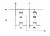
図12はNOR型フラッシュメモリの一般的な回路構成を示している。
図12において、複数のワード線WL、BL(それぞれ2本のみ図示)の各交点には不揮発性トランジスタからなるメモリセルMCが配置されており、各メモリセルMCのコントロールゲートは対応するワード線WLに、ドレインは対応するビット線BLにそれぞれ接続され、全てのソースはソース線SLに共通に接続されている。
【0004】
図13は、図12中の1個のメモリセルMCの素子構造を示す断面図である。半導体基板もしくは半導体基板に形成されたウエル領域等からなる半導体領域101には、この半導体領域101とは反対導電型の拡散領域からなるソース102、ドレイン103が形成されている。さらに上記ソース、ドレイン間のチャネル領域上には図示しないゲート絶縁膜を介してフローティングゲート104が形成され、さらにこのフローティングゲート104上には図示しないゲート絶縁膜を介してコントロールゲート105が形成されている。
【0005】
このような構成のメモリにおいて、データの読み出しは次のようにして行われる。すなわち、選択されたワード線WLに正極性の電圧、例えば5Vを印加し、メモリセルMCのドレインに接続されたビット線BLに電流が流れるか否かで、データの“1”/“0”の判定を行う。“1”セルの場合、ワード線WL(コントロールゲート105)から見た閾値電圧は5V以下であるために、そのメモリセルにはドレイン電流が流れる。一方、“0”セルの場合、ワード線WLから見た閾値電圧は5V以上であるために、そのメモリセルにはドレイン電流は流れない。そして、センスアンプでこの電流差を検知し、外部にセンスデータとして出力する。
【0006】
データの書き込みは次のようにして行われる。すなわち、選択されたワード線WLに正極性の高電圧、例えば10Vを印加し、書き込み選択されたビット線BLには例えば5Vを印加して、ホットエレクトロン注入現象によって閾値電圧を5V以上にすることによって実現される。書き込み非選択のビット線BLには0Vの電圧が印加されるためにホットエレクトロンが発生しないので、閾値電圧は5V以下のままである。なお、データを書き込む前には予め消去を行って全て“1”データにしておき、その後“0”データを選択的に書き込むようにする。
【0007】
データの消去は、複数個のメモリセル(例えば512kビット)に対して一括して行われる。すなわち、ソース線SLに正極性の電圧、例えば5Vを印加し、消去を行うメモリセルに接続されているワード線WLの全てに負極性の電圧、例えば−7Vを印加し、図13中に示されるフローティングゲート104とソース102とのオーバーラップ領域のトンネル酸化膜106を介して、トンネル現象によってフローティングゲート104から電子をソース102に引き抜くことによって実現される。
【0008】
【発明が解決しようとする課題】
ところで、これまでは素子の微細化によってチップサイズを縮小してきたが、メモリサイズに対するフローティングゲートとソースとのオーバーラップ領域が占める割合が増しており、この結果、メモリセルサイズの縮小率が低下する傾向にある。
【0009】
この発明は上記のような事情を考慮してなされたものであり、その目的は、メモリセルサイズの縮小率を向上させることができる不揮発性半導体記憶装置を提供することにある。
【0010】
【課題を解決するための手段】
第1の発明の不揮発性半導体記憶装置は、コントロールゲート、フローティングゲート、ソース及びドレインをそれぞれ有する複数のメモリセルと、上記複数のメモリセルのコントロールゲートに接続された複数のワード線と、上記複数のメモリセルのドレインに接続された複数のビット線と、上記複数のメモリセルのソースに共通に接続され、かつ上記複数のメモリセルが形成されている半導体領域に接続されたソース線と、上記複数のメモリセルに対してデータを書き込むための書き込み手段と、上記複数のメモリセルからデータを読み出すための読み出し手段と、上記複数のメモリセルのデータを消去するための消去手段とを具備し、上記複数のワード線のうち少なくとも1つが上記半導体領域に接続されていることを特徴とする。
【0011】
第2の発明の不揮発性半導体記憶装置は、コントロールゲート、フローティングゲート、ソース及びドレインをそれぞれ有する複数のメモリセルが第1の半導体領域内に形成された第1のメモリセルアレイと、コントロールゲート、フローティングゲート、ソース及びドレインをそれぞれ有する複数のメモリセルが、上記第1の半導体領域と分離された第2の半導体領域内に形成された第2のメモリセルアレイと、上記第1のメモリセルアレイ内の複数のメモリセルのコントロールゲートに接続された複数の第1のワード線と、上記第2のメモリセルアレイ内の複数のメモリセルのコントロールゲートに接続された複数の第2のワード線と、上記第1のメモリセルアレイ内の複数のメモリセルのドレインに接続された複数の第1のビット線と、上記第2のメモリセルアレイ内の複数のメモリセルのドレインに接続された複数の第2のビット線と、上記第1のメモリセルアレイ内の複数のメモリセルのソースに共通に接続され、かつ上記第1の半導体領域に接続された第1のソース線と、上記第2のメモリセルアレイ内の複数のメモリセルのソースに共通に接続され、かつ上記第2の半導体領域に接続された第2のソース線と、上記第1及び第2のメモリセルアレイ内の複数のメモリセルに対してデータを書き込むための書き込み手段と、上記第1及び第2のメモリセルアレイ内の複数のメモリセルからデータを読み出すための読み出し手段と、上記第1及び第2のメモリセルアレイ内の複数のメモリセルのデータを消去するための消去手段とを具備し、上記消去手段は、上記第1のメモリセルアレイ内のメモリセルのデータを消去するときには上記複数の第1のワード線に負極性の電圧を出力しかつ上記第1のソース線に正極性の電圧を出力し、上記第2のメモリセルアレイ内のメモリセルのデータを消去するときには上記複数の第2のワード線に負極性の電圧を出力しかつ上記第2のソース線に正極性の電圧を出力する手段を含んで構成されることを特徴とする。
【0012】
第3の発明の不揮発性半導体記憶装置は、コントロールゲート、フローティングゲート、ソース及びドレインをそれぞれ有し、半導体領域に形成された複数のメモリセルと、上記複数のメモリセルのコントロールゲートに接続された複数のワード線と、上記複数のメモリセルのドレインに接続された複数のビット線と、上記複数のメモリセルのソースに共通に接続されたソース線と、上記複数のメモリセルに対してデータを書き込むための書き込み手段と、上記複数のメモリセルからデータを読み出すための読み出し手段と、上記複数のメモリセルのデータを消去するための消去手段とを具備し、上記消去手段は、上記複数のワード線に負極性の電圧を出力しかつ上記複数のメモリセルが形成されている上記半導体領域に正極性の電圧を出力する手段を含み、上記半導体領域に正極性の電圧が出力された後に上記複数のワード線に負極性の電圧を出力するように構成されており、上記複数のワード線のうち少なくとも1つが上記半導体領域に接続されていることを特徴とする。
【0013】
【発明の実施の形態】
以下、図面を参照してこの発明を実施の形態により説明する。
図1は、この発明に係る不揮発性半導体記憶装置全体の構成を示すブロック図である。この実施の形態による不揮発性半導体記憶装置(以下、メモリ装置と略称する)10は、それぞれ512kビットサイズの複数個のメモリセルアレイ(MCA)(本例では2個)11、12と、ロウメインデコーダ(RM)13及びロウサブデコーダ(RS)14、15から構成されるロウデコーダと、それぞれツリー状に構成され、上記メモリセルアレイ11、12のビット線を選択するカラムゲート(CG)16、17と、ロウメインデコーダ13によって選択されたロウサブデコーダ14または15を介して、メモリセルアレイ11または12内のワード線をバイアスするコントロールゲートドライバ(GD)18、19と、メモリセルアレイ11及び12がそれぞれ形成される互いに分離された2つの半導体領域(ウエル領域)をバイアスするウエルドライバ(WD)20、21と、上記カラムゲート16、17を介してメモリセルアレイ11、12から読み出されるセルデータをセンスし、増幅し、Doutとしてメモリ装置10の外部に出力するセンスアンプ(SA)22と、メモリ装置10の外部から入力される書き込みデータDin に対応した書き込み電圧を、上記カラムゲート16、17を介してメモリセルアレイ11、12のビット線に出力する書き込みバッファ(WB)23と、メモリ装置10の外部から入力されるアドレス信号Add のうちメモリセルアレイブロックアドレスに対応したアドレスから内部メモリセルアレイブロックアドレスを生成するブロックアドレスバッファ(BAB)24と、上記アドレス信号Add のうちロウアドレスに対応したアドレスから内部ロウアドレスを生成するロウアドレスバッファ(RA)25と、上記アドレス信号Add のうちカラムアドレスに対応したアドレスから内部カラムアドレスを生成するカラムアドレスバッファ(CA)26とから構成されている。
【0014】
なお、メモリ装置10の外部からは各種制御信号ctl が入力され、これらの制御信号ctl は先のウエルドライバ20、21、センスアンプ22及び書き込みバッファ23の動作の制御に使用される。
【0015】
図2は、図1中のメモリセルアレイ11、12のうち一方のメモリセルアレイ11の詳細な回路例を示している。なお上記両メモリセルアレイ11、12は共に同様に構成されているので、他方のメモリセルアレイ12についてはその説明を省略する。
【0016】
メモリセルアレイ11には512本のワード線WL0 〜WL511 と1024本のビット線BL0 〜BL1023とが互いに交差するように配列されている。これら各ワード線とビット線との交点にはそれぞれフローティングゲート、コントロールゲート、ソース及びドレインを有する不揮発性トランジスタからなるメモリセルMCが配置されている。これに各メモリセルMCのコントロールゲートは対応するワード線に接続され、ドレインは対応するビット線に接続されている。また、メモリセルMCのうち、ビット線方向で隣接している各2個のメモリセルMCは、ドレインまたはソースのいずれか一方を共有している。さらに全てのメモリセルMCのソースと、バックゲートすなわち各メモリセルMCが形成されているウエル領域(WELL0 )はソース線SLに共通に接続されている。
【0017】
また、メモリセルアレイのビット線方向の両端部には、それぞれ各ワード線に接続されているメモリセルと同数(1024個)の加工用ダミーセルDCからなるダミーセル部DCAがそれぞれ設けられている。上記ダミーセル部DCA内の各ダミーセルDCのコントロールゲート、ソース及びバックゲートは先のソース線SLに接続されている。
【0018】
メモリセルアレイの周辺部ではそれ以外の領域に対してセルの対称性が崩れるため、書き込み時や消去時の特性がメモリセルアレイ中央部のセルのそれらと比べて変ってしまう。例えば、消去時に速く消去される特性であれば、中央部のセルが消去された時に周辺部のセルは消去され過ぎる場合があり、このとき閾値電圧が負になってしまうと、このセルと同じビット線に接続されているセルは例え“0”セルであってもセル電流が流れるので“1”セルと見做されてしまう。これは読み出しエラーを意味する。従って、加工用ダミーセルDCはこの読み出しエラーの発生を防止するために設けられている。すなわち、メモリセルアレイの両端部にそれぞれ1列分の余分なメモリセル(加工用ダミーセルDC)を設けることによって、メモリセルアレイ内のメモリセルの特性を一致を図るようにしている。
【0019】
図3は、図1のメモリ装置10の一部の素子構造を示す断面図である。P型の半導体基板31にはN型のウエル領域32、33が形成されている。上記N型のウエル領域32にはP型のウエル領域34が形成されている。図2中の各メモリセルMCはこのP型のウエル領域34に形成されている。なお、図では1個のメモリセルMCのみ図示している。
【0020】
上記P型のウエル領域34にはこのウエル領域34に対してコンタクトを取るためのP型のコンタクト領域35が、上記N型のウエル領域32にはこのウエル領域32に対してコンタクトを取るためのN型のコンタクト領域36がそれぞれ形成されている。これらのコンタクト領域35、36は、メモリセルMCのソースSと共に前記ソース線SLに接続され、前記ウエルドライバ(WD)20で生成されるバイアスがこのソース線SLを経由してウエル領域32、34及びメモリセルMCのソースSに共通に与えられる。なお、メモリセルMCのドレインDは、図2中の複数のビット線のうち対応するものに接続される。
【0021】
また、上記各メモリセルMCは、フローティングゲートとソースSとの間に、従来のようなオーバーラップ領域を有していない。
一方、N型のウエル領域33にはP型のウエル領域37が形成されており、半導体基板31、上記P型のウエル領域37及びN型のウエル領域33には、メモリ装置10において高電圧が印加されて高耐圧(HV)を要する周辺回路用のNチャネル及びPチャネルMOSトランジスタが形成されている。
【0022】
さらに、P型の半導体基板31にはP型のウエル領域38及びN型のウエル領域39が形成されている。そして、これらP型及びN型のウエル領域38、39には、メモリ装置10において高耐圧を要しない低耐圧(LV)の周辺回路用のNチャネル及びPチャネルMOSトランジスタが形成されている。
【0023】
なお、図示したトランジスタはあくまでも一部であり、半導体基板31には多数のトランジスタが形成されている。
次に、上記構成でなるメモリ装置の動作を説明する。
【0024】
読み出し及び書き込みは従来の場合と同様である。すなわち、読み出しは、ロウメインデコーダ13とロウサブデコーダ14または15によってメモリセルアレイ11または12内のワード線WLが選択され、この選択されたワード線WLに対し、コントロールゲートドライバ(GD)18または19から出力される5Vの電圧が印加される。このとき、ウエルドライバ20、21からは0Vの電圧が出力され、この0Vの電圧が各ソース線SLを介してメモリセルアレイ11、12が形成されているウエル領域WELL(図3中のP型のウエル領域34)に印加される。また、ウエル領域WELLには各メモリセルMCのソースも接続されているので、各メモリセルMCのソースも0Vになる。
【0025】
一方、カラムゲート(CG)16または17を介してメモリセルアレイ11または12内のビット線BLがセンスアンプ22に接続され、選択セルのドレインに接続されたビット線BLに所定の電圧が印加される。このとき、選択セルが“1”セルの場合、ワード線WLから見た閾値電圧は5V以下であるために、そのメモリセルにはドレイン電流が流れる。“0”セルの場合、ワード線WLから見た閾値電圧は5V以上であるために、そのメモリセルにはドレイン電流は流れない。そして、センスアンプ22でこの電流差が検知され、増幅されて外部にセンスデータDoutが出力される。
【0026】
書き込みは、読み出し時と同様にしロウデコーダで選択されたワード線WLに対し、コントロールゲートドライバ18または19から出力される10Vの電圧が印加される。このとき、ウエルドライバ20、21からは0Vの電圧が出力される。
【0027】
この際に、書き込みデータDin に応じて書き込みバッファ(WB)23から出力される5Vの電圧がカラムゲート(CG)16または17を介して、メモリセルアレイ11または12のビット線BLに印加される。従って、選択セルのドレイン、ソース間に電流が流れ、このときに発生するホットエレクトロンがフローティングゲートに注入され、その閾値電圧が5V以上に上昇することによって書き込みが実現される。書き込み非選択のビット線BLには0Vの電圧が印加され、ホットエレクトロンは発生しないので、閾値電圧は5V以下のままである。
【0028】
次に、消去動作について、図4のタイミングチャートを用いて説明する。まず、タイミングT0で消去信号ERASE が“H”にされる。次に、この後のタイミングT1でウエルドライバ20または21から8Vの電圧が出力され、ソース線SLを介してウエル領域WELLが充電され始める。このとき、この8Vの電圧の立上がり勾配は比較的穏やかにされる。その理由は、この8Vの電圧を速く立上げると、ウエル領域との間の容量結合によってワード線WLの電位が上昇し、このワード線WLを選択するロウサブデコーダ14、15を構成するP型のMOSトランジスタのウエル電位よりも高くなり、その結果によって発生するフォワードバイアス状態を避けるためである。
【0029】
ウエル領域WELLが8Vまで充電された後、タイミングT2でコントロールゲートドライバ18または19から−6Vの電圧が出力され、ワード線WLがこの−6Vの電圧で充電され始める。ここで、T1とT2のタイミングを分けている理由は次の通りである。すなわち、ウエルドライバ20、21から出力される8Vの電圧及びコントロールゲートドライバ18、19から出力される−6Vの電圧は、それぞれ図示しない昇圧回路を動作させて生成される。ここで、8Vの電圧を生成する昇圧回路と−6Vの電圧を生成する昇圧回路とを同時に動作させると、お互いの負荷容量を充電することになって、昇圧効率が低下するからである。すなわち、8Vの電圧を生成する昇圧回路がウエル領域を充電している間は、ワード線WLを0Vにすることによって、−6Vの電圧を生成する昇圧回路における消費電流を節約することができる。
【0030】
そして、ウエル領域WELLが8V、ワード線WLが−6Vのときに消去が行われる。すなわち、ワード線WLが−6Vのとき、コントロールゲートとフローティングゲートとの間の容量結合により、フローティングゲートは−6Vよりも絶対値は低いが所定の負の電圧となる。この時、フローティングゲートとメモリセルのチャネル領域全体との間でトンネル電流が流れ、フローティングゲートから電子が引き抜かれ、閾値電圧が5V以下に低下する。このようにして消去が実現される。
【0031】
消去が終了した後は、タイミングT3でコントロールゲートドライバ18または19から0Vの電圧が出力され、ワード線WLが0Vにリセットされる。このリセット動作もゆっくり行う必要がある。これは、ワード線WLを急速に0Vにリセットさせると、ワード線とウエル領域との間の容量結合によってウエル電圧が上がり過ぎてしまい、ウエル領域またはジャンクションブレークダウンを引き起こしてしまうからである。
【0032】
その後、タイミングT4でウエル領域が0Vにリセットされる。このリセット動作もゆっくり行う必要がある。これは、余りにも速すぎると、ワード線とウエル領域との間の容量結合によってワード線電位が負になってしまい、ロウサブデコーダ14、15を構成するN型のMOSトランジスタのウエル電位(0V)よりも低くなってしまい、その結果によって発生するフォワードバイアス状態を避けるためである。
【0033】
この後、タイミングT5で消去信号ERASE が“L”にされて消去動作が終了する。
なお、図4中のCLK1〜CLK4は、上記消去動作を制御する際に使用されるクロック信号であり、これらのクロック信号については後に説明する。
【0034】
このように、データの消去はチャネル領域全体でトンネル電流を流がして行われ、従来のようなフローティングゲートとソースとの間のオーバーラップ領域は形成されていないので、従来に比べてメモリセルサイズの縮小率の向上を図ることができる。
【0035】
また、図3に示すように、メモリセルMCが形成されているP型のウエル領域34と、このウエル領域34が形成されているN型のウエル領域32とは共にソース線SLに接続されている。書き込み時と読み出し時に、ウエル領域34とメモリセルMCのソースSは共に0Vであるので、このウエル領域34とソースSをショートしてよい。また、消去時もウエル領域34とソースSを同電位にバイアスしてよく、両者をショートしてよい。これにより、ウエル配線とソース配線を別々に設ける必要がないので、配線領域と配線を駆動する駆動回路の削減を図ることができる。
【0036】
さらに、消去時に過消去を防いで読み出しエラーの発生を防止する、図2中のダミーセル部DCAにおいて、各ダミーセルDCのコントロールゲートは、ソース線SLに接続されており、メモリセルMCの書き込み時や読み出し時には0Vが印加される。従って、ダミーセルDCのコントロールゲートとウエル領域との間には電圧ストレスが加わらない。
【0037】
一方、メモリセルMCの消去時には、ウエル領域には正極性の電圧(8V)が印加されるが、コントロールゲートとウエル領域とが接続されており、コントロールゲートにもこの正極性の電圧が印加されるので、この場合にもダミーセルDCには電圧ストレスが加わらない。
【0038】
このようにダミーセルDCのコントロールゲートはメモリセルアレイ内でソース線SLに接続することができるので、ダミーセルDCのワード線に対する配線が不要になる。この結果、ダミーセルDCを設けていてもそれに必要な配線領域や駆動回路を無くすことができるので、面積はそれ程増加しない。
【0039】
図5(a)は図1における一方のウエルドライバ(WD)20のシンボル図を示しており、図5(b)はその詳細な回路構成を示している。なお、図1中の他方のウエルドライバ21もこれと同様に構成されており、入力される内部メモリセルアレイブロックアドレス(BA、/BA)のみが異なるので、その説明は省略する。
【0040】
図5(a)に示すように、ウエルドライバ(WD)20には図示しないクロック発生回路で生成されるクロック信号CLK1、CLK2、CLK4と、ブロックアドレスバッファ(BAB)24で生成される内部メモリセルアレイブロックアドレス(以下、単にアドレスと称する)BA0、/BA0が供給され、ウエルドライバ20はこれらの信号及び電源電圧に基づいてウエル(WELL0 )バイアスを出力する。
【0041】
次に図5(b)の回路構成について説明する。なお、図5(b)において、VP8はこの回路に供給される+8Vの電源電圧である。
電源電圧VP8の供給ノード(以下、VP8ノードと称する)と接地電圧のノード(以下、接地ノードと称する)との間にはPチャネルのMOSトランジスタ(以下、Pトランジスタと略称する)P1とNチャネルのMOSトランジスタ(以下、Nトランジスタと略称する)N1のソース、ドレイン間が直列に挿入されている。さらにVP8ノードと接地ノードとの間にはPトランジスタP2とNトランジスタN2のソース、ドレイン間が直列に挿入されている。上記PトランジスタP1のゲートは、上記PトランジスタP2とNトランジスタN2の直列接続ノード41に接続されている。上記PトランジスタP2のゲートは、上記PトランジスタP1とNトランジスタN1の直列接続ノードに接続されている。
【0042】
また、3入力のNORゲート42には、アドレス/BA(/BA0)、クロック信号CLK2がそれぞれ直接に、さらにインバータ43を介してクロック信号CLK1が供給される。そして、このNORゲート42の出力はNトランジスタN1のゲートに供給されると共にインバータ44を介してNトランジスタN2のゲートに供給される。
【0043】
VP8ノードと接地ノードとの間にはPトランジスタP3のソース、ドレイン間、抵抗45及びNトランジスタN3のソース、ドレイン間が直列に接続されている。また、VP8ノードと上記PトランジスタP3及び抵抗45の直列接続ノード46との間には、PトランジスタP4のソース、ドレイン間が接続されている。このPトランジスタP4のゲートはノード46に接続されている。
【0044】
VP8ノードと接地ノードとの間にはPトランジスタP5のソース、ドレイン間とNトランジスタN4のソース、ドレイン間とが直列に接続されている。上記PトランジスタP5のゲートは上記ノード46に接続されている。また、NトランジスタN4のゲートには2入力のNANDゲート47の出力が供給される。このNANDゲート47には消去信号ERASE とアドレスBA(BA0)が供給される。また、上記PトランジスタP5とNトランジスタN4の直列接続ノード48からウエル領域WELLに与える電圧が出力される。
【0045】
VP8ノードと上記ノード48との間にはPトランジスタP6のソース、ドレイン間が接続されている。また、上記ノード48と接地ノードとの間には2個のNトランジスタN5、N6ソース、ドレイン間が直列に接続されている。上記NトランジスタN5のゲートには一定バイアス電圧Vstが供給される。2入力のNANDゲート49にはクロック信号CLK4とアドレスBA(BA0)が供給され、このNANDゲート49の出力はインバータ50を介して上記NトランジスタN6のゲートに供給される。
【0046】
VP8ノードと接地ノードとの間にはPトランジスタP7とNトランジスタN7のソース、ドレイン間が直列に挿入されている。さらにVP8ノードと接地ノードとの間にはPトランジスタP8とNトランジスタN8のソース、ドレイン間が直列に挿入されている。上記PトランジスタP7のゲートは、上記PトランジスタP8とNトランジスタN8の直列接続ノードに接続されている。上記PトランジスタP8のゲートは、上記PトランジスタP7とNトランジスタN7の直列接続ノード51に接続されている。先のPトランジスタP6のゲートはこのノード51に接続されている。
【0047】
また、3入力のNORゲート52には、アドレス/BA(/BA0)、クロック信号CLK4がそれぞれ直接に、さらにインバータ53を介してクロック信号CLK2が供給される。そして、このNORゲート52の出力はNトランジスタN7のゲートに供給されると共にインバータ54を介してNトランジスタN8のゲートに供給される。
【0048】
なお、上記PトランジスタP5に比べてPトランジスタP6の素子サイズが大きく設定されていると共に、上記NトランジスタN5に比べてNトランジスタN4の素子サイズが大きく設定されている。
【0049】
次に、上記構成でなるウエルドライバの動作を、先の図4のタイミングチャートを併用して説明する。なお、このウエルドライバが動作する場合、アドレスBAは“H”であり、/BAは“L”である。
【0050】
消去信号ERASE が“L”のときはNANDゲート47の出力が“H”となり、NトランジスタN4がオンして、ウエルバイアスは0Vになる。次に、タイミングT0で消去信号ERASE が“H”になると、NANDゲート47の出力が“L”となり、いままでオンしていたNトランジスタN4がオフする。
【0051】
タイミングT0からT1の期間では全てのクロック信号CLK1〜CLK4は“L”である。従って、NORゲート42の出力は“L”、これに続くインバータ44の出力は“H”であり、NトランジスタN2がオンしてノード41が“L”になる。さらに、ノード41の信号がゲートに入力するPトランジスタP3がオンし、ノード46はVP8(8V)になり、PトランジスタP4及びP5はオフしている。また、NANDゲート49の出力は“H”、これに続くインバータ50の出力は“L”であり、NトランジスタN6はオフしている。NORゲート52の出力は“L”、これに続くインバータ54の出力は“H”であり、NトランジスタN8がオンしてノード51が“H”(VP8)になる。従って、このノード51の信号がゲートに入力するPトランジスタP6はオフしている。
【0052】
次に、タイミングT1にクロック信号CLK1が“H”に立ち上がると、NORゲート42の出力が“H”、これに続くインバータ44の出力が“L”になり、NトランジスタN1がオンしてPトランジスタP1との接続ノードが“L”になる。これにより、PトランジスタP2がオンして、ノード41が“H”(VP8)になる。そして、このノード41信号がゲートに入力するNトランジスタN3がオンし、抵抗45を介して一定電流がPトランジスタP4に流れる。ここで、PトランジスタP4とP5とはカレントミラー回路を構成しているので、上記抵抗45に流れる一定電流がPトランジスタP5側にも流れ、ノード48の充電が開始される。このとき、上記抵抗45に流れる電流の値が比較的小さくなるように設定されているので、先にも説明したようにソース線SLを介してウエル領域WELLが充電され始めときに、8Vの電圧の立上がり勾配は比較的穏やかになる。
【0053】
次に、タイミングT2にクロック信号CLK2が“H”に立ち上がると、NORゲート52の出力が“H”、これに続くインバータ54の出力が“L”になり、NトランジスタN7がオンし、PトランジスタP7との接続ノード51が“L”になる。これにより、素子サイズが大きいPトランジスタP6がオンして、ノード48が十分に大きな電流で充電され始める。
【0054】
次に、タイミングT4にクロック信号CLK4が“H”に立ち上がると、NORゲート52の出力が再び“L”に落ち、これに続くインバータ54の出力が“H”に立ち上がり、NトランジスタN8がオンしてノード51が再び“H”になり、PトランジスタP6がオフして、ノード48に対する充電が終わる。また、クロック信号CLK4が“H”に立ち上がることにより、NANDゲート49の出力が“H”から“L”に落ち、これに続くインバータ50の出力が“L”から“H”に立ち上がり、NトランジスタN6がオンする。ここで、このNトランジスタN6に対して直列接続されているNトランジスタN5のゲートには一定バイアス電圧Vstが供給されているので、NトランジスタN6がオンした後にノード48が放電され始める。この場合、NトランジスタN5の素子サイズが小さくされているので、先にも述べたようにノード48の放電、すなわちリセット動作がゆっくりと行われる。
【0055】
次に、タイミングT5の後に消去信号ERASE が“L”に落ち、全てのクロック信号CLK1〜CLK4が“L”に落ちて、最初の状態に戻る。
図6(a)は、消去時に、ワード線に出力される−6Vの電圧を出力制御する制御回路(BB)のシンボル図を示しており、図6(b)はその詳細な回路構成を示している。
【0056】
図6(a)に示すように、この制御回路(BB)には図示しないクロック発生回路で生成されるクロック信号CLK2、CLK3、ブロックアドレスバッファ(BAB)24で生成されるアドレス/BA及び5Vと−6Vの電源電圧が供給され、この制御回路(BB)はこれらの信号及び電源電圧に基づいてワード線WLに供給するための電圧VBBを出力する。
【0057】
次に図6(b)の回路構成について説明する。なお、図6(b)において、Vcc、VN6はこの回路に供給される5V、−6Vの電源電圧である。
電源電圧Vccの供給ノード(以下、Vccノードと称する)と電源電圧VN6の供給ノード(以下、VN6ノードと称する)との間にはPトランジスタP11とNトランジスタN11のソース、ドレイン間が直列に挿入されている。さらにVccノードとVN6ノードとの間にはPトランジスタP12とNトランジスタN12のソース、ドレイン間が直列に挿入されている。上記NトランジスタN11のゲートは、上記PトランジスタP12とNトランジスタN12の直列接続ノード61に接続されている。上記NトランジスタN12のゲートは、上記PトランジスタP11とNトランジスタN11の直列接続ノード62に接続されている。また、3入力のNORゲート63には、アドレス/BA、クロック信号CLK3がそれぞれ直接に、さらにインバータ64を介してクロック信号CLK2が供給される。そして、このNORゲート63の出力はPトランジスタP11のゲートに供給されると共にインバータ65を介してPトランジスタP12のゲートに供給される。
【0058】
電圧VBBが出力されるノード66とVN6ノードとの間にはNトランジスタN13のソース、ドレイン間が接続され、さらにノード66と接地ノードとの間には1個のPトランジスタP13及び2個のNトランジスタN14、N15の各ソース、ドレイン間が並列に接続されている。上記PトランジスタP13のバックゲート、すなわちこのトランジスタが形成されているウエル領域には5Vの電源電圧Vccが供給され、2個のNトランジスタN14、N15のバックゲートには−6Vの電源電圧VN6が供給されている。
【0059】
上記NトランジスタN13及びPトランジスタP13の各ゲートは上記ノード61に接続され、上記NトランジスタN14のゲートは上記PトランジスタP11とNトランジスタN11の直列接続ノード62に接続されている。
【0060】
VccノードとVN6ノードとの間にはPトランジスタP14のソース、ドレイン間とNトランジスタN16のソース、ドレイン間とが直列に接続されている。さらにVccノードとVN6ノードとの間にはPトランジスタP15とNトランジスタN17のソース、ドレイン間が直列に挿入されている。上記NトランジスタP16のゲートは、上記PトランジスタP15とNトランジスタN17の直列接続ノードに接続されている。上記PトランジスタP17のゲートは、上記PトランジスタP14とNトランジスタN16との直列接続ノード67に接続されている。そして、先のNトランジスタN15のゲートはこのノード67に接続されている。上記PトランジスタP13のゲートに消去信号ERASE が供給され、さらに上記PトランジスタP14のゲートにはインバータ68を介してこの消去信号ERASE が供給される。
【0061】
なお、NトランジスタN14に比べてNトランジスタN15の素子サイズが大きくされていて、NトランジスタN15が流し得る電流の値がNトランジスタN14に比べて大きくされている。
【0062】
次に、図6(b)のような構成でなる制御回路の動作を説明する。なお、この制御回路が動作する場合、アドレス/BAは“L”である。
まず、消去期間ではない消去信号ERASE が“L”の期間(書き込み時及び読み出し時も含む)のとき、インバータ68の出力が“H”となり、これによりPトランジスタP14がオン、PトランジスタP15がオフし、ノード67は“H”(Vcc)となる。このノード67の信号がゲートに供給されるNトランジスタN15がオンし、ノード66が放電されて、VBBは接地電圧の0Vに設定される。
【0063】
一方、消去期間のときは消去信号ERASE が“H”になり、インバータ68の出力が“L”となるので、ノード67が“L”(VN6)となり、NトランジスタN15はオフする。
【0064】
ここで、先の図4のタイミングチャートのタイミングT2以前、すなわちクロック信号CLK2、CLK3が共に“L”の時は、インバータ64の出力が“H”、NORゲート63の出力が“L”、及びこれに続くインバータ65の出力が“H”となり、PトランジスタP11とNトランジスタN12がオンし、PトランジスタP12とNトランジスタN11がオフし、ノード61が“L”(VN6)、ノード62が“H”(Vcc)となる。このとき、ノード61の信号がゲートに入力するNトランジスタN13がオフし、PトランジスタP13がオンする。さらに、ノード62の信号がゲートに入力するNトランジスタN14がオンする。従って、クロック信号CLK2、CLK3が共に“L”の時、ノード66はそれぞれオン状態であるPトランジスタP13とNトランジスタN14を介して放電されて、VBBは接地電圧の0Vに設定される。
【0065】
次に、図4のタイミングチャートのタイミングT2で一方のクロックCLK2が“H”に立ち上がると、インバータ64の出力が“H”から“L”に反転し、MORゲート63の出力は“L”から“H”に反転し、さらにインバータ66の出力が“H”から“L”に反転する。これにより、PトランジスタP12とNトランジスタN11がオンし、PトランジスタP11とNトランジスタN12がオフし、ノード61は“L”(VN6)から“H”(Vcc)へ、また、ノード62は“H”(Vcc)から“L”(VN6)へそれぞれ変化する。このとき、NトランジスタN13がオンし、いままでオンしていたPトランジスタP13とNトランジスタN14がオフする。従って、クロック信号CLK2が“H”に立ち上がった後は、ノード66が電源電圧VN6によって充電され、VBBは−6Vに向かって変化していく。
【0066】
この後、図4のタイミングチャートのタイミングT3で他方のクロックCLK3が“H”に立ち上がると、NORゲート63の出力が再び“L”となり、タイミングT2以前と場合と同様にPトランジスタP13とNトランジスタN14がオンし、ノード66が放電されて、VBBが接地電圧の0Vに設定される。
【0067】
すなわち、図6に示した制御回路では、図4のタイミングチャートのタイミングT2からT3の期間に、VBBとして−6Vの電圧が出力され、その他の期間では0Vになる。
【0068】
図7(a)は、図1中のロウメインデコーダ(RM)13内の1個の部分デコーダのシンボル図を示しており、図7(b)はその詳細な回路構成を示している。
【0069】
図7(a)に示すように、このロウメインデコーダ13の部分デコーダには、後述するプリデコーダから出力されるプリデコード信号GAi、GBj(ただしi、jはそれぞれ0〜7)が供給され、この部分デコーダはメインデコード信号Mij、/Mijを出力する。ここで、i、jの数はそれぞれ8なので、先のロウメインデコーダ13内には、図7(a)に示す部分デコーダが8×8の64個設けられている。
【0070】
次に図7(b)の回路構成について説明する。なお、図7(b)において、VSWはこの部分デコーダに供給される電源電圧であり、その値はデータの読み出し時には5V、書き込み時には10Vになる。また、VBBは図6の回路から出力される電圧である。
【0071】
電源電圧VSWの供給ノード(以下、VSWノードと称する)と接地電圧ノードとの間にはPトランジスタP21とNトランジスタN21のソース、ドレイン間が直列に挿入されている。さらにVSWノードと接地電圧ノードとの間にはPトランジスタP22とNトランジスタN22のソース、ドレイン間が直列に挿入されている。上記PトランジスタP21のゲートは、上記PトランジスタP22とNトランジスタN22の直列接続ノード71に接続されている。上記PトランジスタP22のゲートは、上記PトランジスタP21とNトランジスタN21の直列接続ノード72に接続されている。また、2入力のNANDゲート73にはプリデコード信号GAi及びその相補信号のいずれか一方と、プリデコード信号GBj及びその相補信号のいずれか一方とが供給される。なお、図では、プリデコード信号GAiとGBjが供給されるものについて示している。このNANDゲート73の出力はNトランジスタN21のゲートに供給されると共にインバータ74を介してNトランジスタN22のゲートに供給される。
【0072】
VSWノードと接地電圧ノードとの間にはPトランジスタP23とNトランジスタN23のソース、ドレイン間が直列に挿入されている。さらにVSWノードと接地電圧ノードとの間にはPトランジスタP24とNトランジスタN24のソース、ドレイン間が直列に挿入されている。上記PトランジスタP23のゲートは先のノード71に接続され、上記PトランジスタP24のゲートは先のノード72に接続されている。そして、PトランジスタP23とNトランジスタN23の直列接続ノード75からメインデコード信号Mijが出力され、PトランジスタP24とNトランジスタN24の直列接続ノード76からメインデコード信号/Mijが出力される。
【0073】
図7(b)の部分デコーダにおいて、図中のプリデコード信号GAi、GBjが共に“H”のとき、すなわち、図示の部分デコーダが選択される条件の時、NANDゲート73の出力が“L”、これに続くインバータ74の出力が“H”となり、NトランジスタN21がオフし、NトランジスタN22がオンする。これによりノード71が“L”となり、さらにPトランジスタP21がオンして、ノード72が“H”(VSW)となり、PトランジスタP22がオフする。
【0074】
従って、PトランジスタP23がオンし、PトランジスタP24がオフする。また、PトランジスタP23がオンすると、ノード75が“H”(VSW)となり、NトランジスタN24がオンする。これにより、ノード76が“L”となり、NトランジスタN23はオフする。
【0075】
すなわち、プリデコード信号GAi、GBjが共に“H”のときにメインデコード信号Mij、/Mijは“H”、“L”となり、選択状態となる。
また、これ以外の部分デコーダでは、NANDゲート73に入力される2つのプリデコード信号のうち少なくともいずれか一方が“L”になり、そのNANDゲート73の出力が“H”、そのインバータ74の出力が“L”になるので、それぞれのメインデコード信号Mij、/Mijは“L”、“H”となり、非選択状態となる。
【0076】
図8(a)は、ロウメインデコーダ13から出力されるメインデコード信号Mij、/Mij及び図1中のコントロールゲートドライバ(GD)18もしくは19の出力Fkが供給される図1中のロウサブデコーダ(RS)14もしくは15内の1個の部分デコーダのシンボル図を示しており、図8(b)はその詳細な回路構成を示している。
【0077】
ここで、先にも述べたようにi、jの数はそれぞれ8であり、また、kの数も8にされているので、各ロウサブデコーダ内には図8(a)に示す部分デコーダが64×8の512個設けられており、それぞれの出力は512本のワード線 WLijk(図2中のWL0 〜WL511 )のうち対応する1本に出力される。
【0078】
次に8(b)の回路構成について説明する。8(b)に示す部分デコーダは、NトランジスタN25及びPトランジスタP25からなり、コントロールゲートドライバ18もしくは19の出力Fkのノードと対応するワード線WLijkとの間に挿入されたCMOS型のトランスファゲート77と、ワード線WLijkと図6の回路から出力される電圧VBBのノードとの間に接続されたNトランジスタN26とから構成されている。そして、NトランジスタN25及びPトランジスタP25の各ゲートには図7のロウメインデコーダで発生されるメインデコード信号Mij、/Mijが供給され、NトランジスタN26のゲートにはメインデコード信号/Mijが供給される。
【0079】
このように構成されたロウサブデコーダの部分デコーダでは、メインデコード信号Mij、/Mijが“H”、“L”のときは、トランスファゲート77がオンし、コントロールゲートドライバ18もしくは19の出力Fkがワード線WLijkに出力される。
【0080】
他方、メインデコード信号Mij、/Mijが“L”、“H”のときには、トランスファゲート77はオフし、NトランジスタN26がオンして、電圧VBBがワード線WLijkに出力される。
【0081】
図9(a)は、図1中のコントロールゲートドライバ(GD)18もしくは19内の1個のドライバ回路のシンボル図を示しており、図9(b)はその詳細な回路構成を示している。
【0082】
ここで、コントロールゲートドライバ18もしくは19には、図1中のロウアドレスバッファ(RA)25で生成される3ビットの内部ロウアドレスRA0、/RA0〜RA2、/RA2が入力される。従って、各コントロールゲートドライバ内には図8(a)、(b)に示すようなドライバ回路がそれぞれ8個設けられている。図9(b)はこの8個のドライバ回路のうち、アドレス/RA0、/RA1、/RA2が入力されてF0(k=0)を出力するものを例示しているが、他のドライバ回路もこれと同様に構成されており、入力信号が異なるだけであるので、その説明は省略する。
【0083】
図9(b)において、VSWノードと接地電圧ノードとの間にはPトランジスタP31とNトランジスタN31のソース、ドレイン間が直列に挿入されている。さらにVSWノードと接地電圧ノードとの間にはPトランジスタP32とNトランジスタN32のソース、ドレイン間が直列に挿入されている。上記PトランジスタP31のゲートはPトランジスタP32とNトランジスタN32の直列接続ノード81に接続され、上記PトランジスタP34のゲートはPトランジスタP31とNトランジスタN31の直列接続ノードに接続されている。
【0084】
また、3入力のNANDゲート82には3ビットのアドレス/RA0、/RA1、/RA2が入力される。このNANDゲート82の出力はインバータ83を介してNトランジスタN31のゲートに供給され、さらにインバータ83の出力はインバータ84を介してNトランジスタN32のゲートに供給される。そして、F0は上記ノード81から出力される。
【0085】
このような構成の回路において、3ビットのアドレス/RA0、/RA1、/RA2が全て“H”、すなわちこのドライブ回路が選択される条件のときは、NANDゲート82の出力が“L”、インバータ83の出力が“H”、インバータ84の出力が“L”となり、NトランジスタN31がオン、NトランジスタN32がオフし、出力F0は“H”(VSW)になる。
【0086】
このとき、これ以外の7個のドライバ回路では、3ビットのアドレスのうち少なくとも1つが“L”となっているので、NANDゲート82の出力は“H”、インバータ83の出力は“L”、インバータ84の出力は“H”となり、NトランジスタN31がオフ、NトランジスタN32がオンし、出力F0は“L”(接地電圧)になる。
【0087】
図10(a)、(b)は、先の図7に示したロウメインデコーダ(RM)13内の部分デコーダに入力されるプリデコード信号GAi、GBj(i、jはそれぞれ0〜7)を生成するプリデコーダの詳細な回路構成を示している。
【0088】
プリデコード信号GAi(GA0〜GA7)を生成する8個の各プリデコーダは、図10(a)に示すように、それぞれ3入力のNANDゲート82とインバータ83とから構成されている。上記NANDゲート82には、3ビットの内部ロウアドレスRA3、RA4、RA5及びこれらの相補アドレス/RA3、/RA4、/RA5の組み合わせが入力され、これら各NANDゲート82の出力がインバータ83で反転されることによってプリデコード信号GAi(GA0〜GA7)が出力される。
【0089】
図10(b)に示す、プリデコード信号GBi(GB0〜GB7)を生成する8個の各プリデコーダは、図10(a)に示すものど同様にNANDゲート82とインバータ83とから構成されている。なお、この場合、3ビットの内部ロウアドレスRA3、RA4、RA5及びこれらの相補アドレス/RA3、/RA4、/RA5の代わりに、3ビットの内部ロウアドレスRA6、RA7、RA8及びこれらの相補アドレス/RA6、/RA7、/RA8の組み合わせが入力され、各インバータ83からはプリデコード信号GBi(GB0〜GB7)が出力される。
【0090】
図11は、図6に示した制御回路(BB)、図7に示したロウメインデコーダ(RM)13及び図8に示したロウサブデコーダ(RS)14(15)からなるロウデコーダ全体の構成を示すブロックである。各ワード線WLはロウサブデコーダ内の一つの部分デコーダRPDに接続され、さらに8個の部分デコーダRPDはロウメインデコーダ13内の1つの部分デコーダRMDからの出力Mij、/Mijで制御される。また、コントロールゲートドライバ18(19)の出力F0〜F7は、ロウサブデコーダ内の部分デコーダRPDに8個おきに順次入力される。
【0091】
先に説明したように、ロウメインデコーダ13内には部分デコーダRMDが64個設けられており、それぞれの出力が各8個の部分デコーダRPDに供給される。
【0092】
ここで、書き込み時や読み出し時は、ロウアドレスRA0〜RA8で選択される1つのワード線に電圧VSWが出力され、その他のワード線には電圧VBBが出力される。電圧VSWは先にも述べたように、書き込み時は10Vに、読み出し時は5Vにされ、電圧VBBは書き込み時及び読み出し時は共に0Vにされる。
【0093】
なお、この発明は上記実施の形態に限定されるものではなく種々の変形が可能であることはいううまでもない。例えば、図1中のメモリセルアレイ11、12内のメモリセルが、図3に示すようにN型のウエル領域32に形成されたP型のウエル領域34に設けられる場合について説明したが、これに限定されるものではなく、メモリセルをP型の半導体基板31に設けるようにしてもよい。このようにメモリセルをP型の半導体基板31に設けた場合、ソース線SLはメモリセルのソースに接続されると共にP型の半導体基板31にも接続される。
【0094】
【発明の効果】
以上説明したようにこの発明によれば、メモリセルサイズの縮小率を向上させることができる不揮発性半導体記憶装置を提供することができる。
【図面の簡単な説明】
【図1】この発明に係る不揮発性半導体記憶装置全体の構成を示すブロック図。
【図2】図1中のメモリセルアレイの一方の詳細な回路例を示す回路図。
【図3】図1のメモリ装置の一部の素子構造を示す断面図。
【図4】図1のメモリ装置の消去動作を説明するためのタイミングチャート。
【図5】図5(a)は図1における一方のウエルドライバのシンボル図、図5(b)はその詳細な回路構成を示す回路図。
【図6】図6(a)は消去時にワード線に出力される−6Vの電圧を出力制御する制御回路のシンボル図、図6(b)はその詳細な回路構成を示す回路図。
【図7】図7(a)は図1中のロウメインデコーダ内の1個の部分デコーダのシンボル図、図7(b)はその詳細な回路構成を示す回路図。
【図8】図8(a)は図1中のロウサブデコーダ内の1個の部分デコーダのシンボル図、図8(b)はその詳細な回路構成を示す回路図。
【図9】図9(a)は図1中のコントロールゲートドライバ内の1個のドライバ回路のシンボル図、図9(b)はその詳細な回路構成を示す回路図。
【図10】図10(a)はプリデコード信号GAiを生成するプリデコーダの詳細な回路構成を示す回路図、図10(b)はプリデコード信号GBjを生成するプリデコーダの詳細な回路構成を示す回路図。
【図11】図6の制御回路と図7のロウメインデコーダ及び図8のロウサブデコーダからなるロウデコーダ全体の構成を示すブロック。
【図12】NOR型フラッシュメモリの一般的な回路構成を示す図。
【図13】図12中の1個のメモリセルの素子構造を示す断面図。
【符号の説明】
10…不揮発性半導体記憶装置(メモリ装置)、
11、12…メモリセルアレイ(MCA)、
13…ロウメインデコーダ(RM)、
14、15…ロウサブデコーダ(RS)、
16、17…カラムゲート(CG)、
18、19…コントロールゲートドライバ(GD)、
20、21…ウエルドライバ(WD)、
22…センスアンプ(SA)、
23…書き込みバッファ(WB)、
24…ブロックアドレスバッファ(BAB)、
25…ロウアドレスバッファ(RA)、
26…カラムアドレスバッファ(CA)、
31…P型の半導体基板、
32、33…N型のウエル領域、
34…P型のウエル領域、
35…P型のコンタクト領域、
36…N型のコンタクト領域、
37…P型のウエル領域、
38…P型のウエル領域、
39…N型のウエル領域。
WL0 〜WL511 …ワード線、
BL0 〜BL1023…ビット線、
MC…メモリセル、
SL…ソース線、
DC…加工用ダミーセル、
DCA…ダミーセル部。[0001]
BACKGROUND OF THE INVENTION
The present invention relates to a nonvolatile semiconductor memory device, and more particularly to a nonvolatile semiconductor memory device having an improved data erasing method in a memory cell.
[0002]
[Prior art]
One type of nonvolatile semiconductor memory device is a NOR flash memory. As a conventional NOR type flash memory, for example, one described in “IEEE-Journal of Solid-State Circuits, vol. 27, No. 11, pp. 1540-1546, Nov. 1992” is well known.
[0003]
FIG. 12 shows a general circuit configuration of a NOR type flash memory.
In FIG. 12, a memory cell MC composed of a nonvolatile transistor is arranged at each intersection of a plurality of word lines WL and BL (only two are shown), and the control gate of each memory cell MC is a corresponding word line WL. The drains are connected to the corresponding bit lines BL, respectively, and all the sources are connected to the source line SL in common.
[0004]
FIG. 13 is a cross-sectional view showing the element structure of one memory cell MC in FIG. In a
[0005]
In the memory having such a configuration, data reading is performed as follows. That is, a positive voltage, for example, 5 V is applied to the selected word line WL, and data “1” / “0” is determined depending on whether or not a current flows through the bit line BL connected to the drain of the memory cell MC. Judgment is made. In the case of the “1” cell, since the threshold voltage viewed from the word line WL (control gate 105) is 5 V or less, a drain current flows through the memory cell. On the other hand, in the case of the “0” cell, since the threshold voltage viewed from the word line WL is 5 V or higher, no drain current flows through the memory cell. Then, this current difference is detected by the sense amplifier and outputted to the outside as sense data.
[0006]
Data writing is performed as follows. That is, a positive high voltage, for example, 10 V is applied to the selected word line WL, and 5 V is applied to the write-selected bit line BL, for example, so that the threshold voltage is set to 5 V or more by hot electron injection phenomenon. It is realized by. Since a voltage of 0V is applied to the write non-selected bit line BL, hot electrons are not generated, so the threshold voltage remains at 5V or less. Before data is written, the data is erased in advance and set to all “1” data, and then “0” data is selectively written.
[0007]
Data is erased collectively for a plurality of memory cells (for example, 512 kbits). That is, a positive voltage, for example, 5V is applied to the source line SL, and a negative voltage, for example, -7V is applied to all the word lines WL connected to the memory cell to be erased, as shown in FIG. This is realized by extracting electrons from the
[0008]
[Problems to be solved by the invention]
By the way, although the chip size has been reduced by miniaturization of elements so far, the ratio of the overlap region between the floating gate and the source to the memory size has increased, and as a result, the reduction rate of the memory cell size has decreased. There is a tendency.
[0009]
The present invention has been made in view of the above circumstances, and an object thereof is to provide a nonvolatile semiconductor memory device capable of improving the reduction rate of the memory cell size.
[0010]
[Means for Solving the Problems]
According to a first aspect of the present invention, there is provided a nonvolatile semiconductor memory device including a plurality of memory cells each having a control gate, a floating gate, a source, and a drain, a plurality of word lines connected to the control gates of the plurality of memory cells, and the plurality of memory cells A plurality of bit lines connected to the drains of the memory cells, a source line connected in common to the sources of the plurality of memory cells and connected to a semiconductor region in which the plurality of memory cells are formed, and A writing means for writing data to a plurality of memory cells, a reading means for reading data from the plurality of memory cells, and an erasing means for erasing data of the plurality of memory cells,At least one of the plurality of word lines is connected to the semiconductor region. It is characterized by that.
[0011]
According to a second aspect of the present invention, there is provided a nonvolatile semiconductor memory device including a first memory cell array in which a plurality of memory cells each having a control gate, a floating gate, a source and a drain are formed in a first semiconductor region, a control gate, and a floating gate A plurality of memory cells each having a gate, a source, and a drain; a second memory cell array formed in a second semiconductor region separated from the first semiconductor region; and a plurality of memory cells in the first memory cell array A plurality of first word lines connected to the control gates of the memory cells; a plurality of second word lines connected to the control gates of the plurality of memory cells in the second memory cell array; A plurality of first bit lines connected to drains of a plurality of memory cells in the memory cell array; A plurality of second bit lines connected to the drains of the plurality of memory cells in the second memory cell array, and a source connected to the sources of the plurality of memory cells in the first memory cell array; A first source line connected to one semiconductor region and a second source connected in common to the sources of a plurality of memory cells in the second memory cell array and connected to the second semiconductor region Lines, writing means for writing data to the plurality of memory cells in the first and second memory cell arrays, and reading data from the plurality of memory cells in the first and second memory cell arrays. Reading means, and erasing means for erasing data of a plurality of memory cells in the first and second memory cell arrays,The erasing means outputs a negative voltage to the plurality of first word lines and applies a positive voltage to the first source line when erasing data of the memory cells in the first memory cell array. When outputting and erasing data in the memory cells in the second memory cell array, a negative voltage is output to the plurality of second word lines and a positive voltage is output to the second source line. Comprising means It is characterized by that.
[0012]
A nonvolatile semiconductor memory device according to a third aspect of the present invention has a control gate, a floating gate, a source and a drain, and is connected to a plurality of memory cells formed in the semiconductor region and the control gates of the plurality of memory cells. A plurality of word lines, a plurality of bit lines connected to drains of the plurality of memory cells, a source line commonly connected to sources of the plurality of memory cells, and data to the plurality of memory cells Writing means for writing, reading means for reading data from the plurality of memory cells, and erasing means for erasing data of the plurality of memory cells, the erasing means comprising the plurality of words A negative voltage is output to the line and a positive voltage is output to the semiconductor region where the plurality of memory cells are formed. Includes means that, configured to output a negative voltage to the plurality of word lines after the voltage of the positive polarity to the semiconductor region is outputAnd at least one of the plurality of word lines is connected to the semiconductor region. It is characterized by that.
[0013]
DETAILED DESCRIPTION OF THE INVENTION
Embodiments of the present invention will be described below with reference to the drawings.
FIG. 1 is a block diagram showing the configuration of the entire nonvolatile semiconductor memory device according to the present invention. A nonvolatile semiconductor memory device (hereinafter abbreviated as a memory device) 10 according to this embodiment includes a plurality of memory cell arrays (MCAs) (two in this example) 11 and 12 each having a 512 kbit size, and a row main decoder. (RM) 13 and row sub-decoders (RS) 14 and 15; and column gates (CG) 16 and 17 for selecting bit lines of the
[0014]
Various control signals ctl are input from the outside of the
[0015]
FIG. 2 shows a detailed circuit example of one of the
[0016]
In the
[0017]
In addition, dummy cell portions DCA each including the same number (1024) of processing dummy cells DC as the memory cells connected to each word line are provided at both ends in the bit line direction of the memory cell array. The control gate, source and back gate of each dummy cell DC in the dummy cell portion DCA are connected to the previous source line SL.
[0018]
In the peripheral portion of the memory cell array, the symmetry of the cells is lost with respect to other regions, so that the characteristics at the time of writing and erasing change compared to those of the cells in the central portion of the memory cell array. For example, in the case of a characteristic that is quickly erased at the time of erasing, the peripheral cell may be over-erased when the central cell is erased, and if the threshold voltage becomes negative at this time, the same as this cell Even if the cell connected to the bit line is a “0” cell, a cell current flows, so that it is regarded as a “1” cell. This means a read error. Therefore, the processing dummy cell DC is provided to prevent the occurrence of this read error. That is, by providing extra memory cells (processing dummy cells DC) for one column at both ends of the memory cell array, the characteristics of the memory cells in the memory cell array are matched.
[0019]
FIG. 3 is a cross-sectional view showing a part of the element structure of the
[0020]
The P-
[0021]
Each memory cell MC does not have an overlap region as in the conventional case between the floating gate and the source S.
On the other hand, a P-
[0022]
Further, a P-
[0023]
Note that the illustrated transistor is only a part, and a large number of transistors are formed on the
Next, the operation of the memory device configured as described above will be described.
[0024]
Reading and writing are the same as in the conventional case. That is, in the read operation, the word line WL in the
[0025]
On the other hand, the bit line BL in the
[0026]
For writing, the voltage of 10 V output from the
[0027]
At this time, a voltage of 5V output from the write buffer (WB) 23 according to the write data Din is applied to the bit line BL of the
[0028]
Next, the erase operation will be described with reference to the timing chart of FIG. First, the erase signal ERASE is set to “H” at timing T0. Next, a voltage of 8V is output from the
[0029]
After the well region WELL is charged to 8V, a voltage of −6V is output from the
[0030]
Erase is performed when the well region WELL is 8V and the word line WL is -6V. That is, when the word line WL is -6V, the floating gate has a predetermined negative voltage although its absolute value is lower than -6V due to capacitive coupling between the control gate and the floating gate. At this time, a tunnel current flows between the floating gate and the entire channel region of the memory cell, electrons are extracted from the floating gate, and the threshold voltage decreases to 5 V or less. In this way, erasure is realized.
[0031]
After erasing is completed, a voltage of 0V is output from the
[0032]
Thereafter, the well region is reset to 0 V at timing T4. This reset operation also needs to be performed slowly. If this is too fast, the word line potential becomes negative due to capacitive coupling between the word line and the well region, and the well potential (0 V) of the N-type MOS transistors constituting the row sub-decoders 14 and 15. This is in order to avoid a forward bias state that occurs as a result.
[0033]
Thereafter, at timing T5, the erase signal ERASE is set to "L" and the erase operation is completed.
Note that CLK1 to CLK4 in FIG. 4 are clock signals used when controlling the erasing operation, and these clock signals will be described later.
[0034]
As described above, data is erased by flowing a tunnel current through the entire channel region, and the conventional overlap region between the floating gate and the source is not formed. The size reduction rate can be improved.
[0035]
As shown in FIG. 3, the P-
[0036]
Further, in the dummy cell section DCA in FIG. 2 which prevents over-erasure at the time of erasure and prevents the occurrence of a read error, the control gate of each dummy cell DC is connected to the source line SL, and when the memory cell MC is written, At the time of reading, 0V is applied. Therefore, no voltage stress is applied between the control gate of the dummy cell DC and the well region.
[0037]
On the other hand, when erasing the memory cell MC, a positive voltage (8V) is applied to the well region, but the control gate and the well region are connected, and this positive voltage is also applied to the control gate. Therefore, in this case as well, no voltage stress is applied to the dummy cell DC.
[0038]
Thus, since the control gate of the dummy cell DC can be connected to the source line SL in the memory cell array, wiring for the word line of the dummy cell DC becomes unnecessary. As a result, even if the dummy cell DC is provided, the wiring area and the drive circuit necessary for the dummy cell DC can be eliminated, so that the area does not increase so much.
[0039]
FIG. 5A shows a symbol diagram of one well driver (WD) 20 in FIG. 1, and FIG. 5B shows its detailed circuit configuration. The
[0040]
As shown in FIG. 5A, the well driver (WD) 20 has an internal memory cell array generated by clock signals CLK1, CLK2, and CLK4 generated by a clock generation circuit (not shown) and a block address buffer (BAB) 24. Block addresses (hereinafter simply referred to as addresses) BA0 and / BA0 are supplied, and the
[0041]
Next, the circuit configuration of FIG. 5B will be described. In FIG. 5B, VP8 is a power supply voltage of + 8V supplied to this circuit.
P channel MOS transistor (hereinafter abbreviated as P transistor) P1 and N channel between a supply node (hereinafter referred to as VP8 node) of power supply voltage VP8 and a node of ground voltage (hereinafter referred to as ground node) The source and drain of a MOS transistor (hereinafter abbreviated as N transistor) N1 is inserted in series. Further, the source and drain of the P transistor P2 and the N transistor N2 are inserted in series between the VP8 node and the ground node. The gate of the P transistor P1 is connected to the
[0042]
Further, the address / BA (/ BA0) and the clock signal CLK2 are directly supplied to the three-input NOR
[0043]
Between the VP8 node and the ground node, the source and drain of the P transistor P3, and the
[0044]
Between the VP8 node and the ground node, the source and drain of the P transistor P5 and the source and drain of the N transistor N4 are connected in series. The gate of the P transistor P5 is connected to the
[0045]
Between the VP8 node and the
[0046]
Between the VP8 node and the ground node, the source and drain of the P transistor P7 and the N transistor N7 are inserted in series. Further, the source and drain of the P transistor P8 and the N transistor N8 are inserted in series between the VP8 node and the ground node. The gate of the P transistor P7 is connected to the series connection node of the P transistor P8 and the N transistor N8. The gate of the P transistor P8 is connected to the
[0047]
Further, the address / BA (/ BA0) and the clock signal CLK4 are directly supplied to the 3-input NOR
[0048]
The element size of the P transistor P6 is set larger than that of the P transistor P5, and the element size of the N transistor N4 is set larger than that of the N transistor N5.
[0049]
Next, the operation of the well driver configured as described above will be described with reference to the timing chart of FIG. When the well driver operates, the address BA is “H” and / BA is “L”.
[0050]
When the erase signal ERASE is “L”, the output of the
[0051]
In the period from the timing T0 to T1, all the clock signals CLK1 to CLK4 are “L”. Accordingly, the output of the NOR
[0052]
Next, when the clock signal CLK1 rises to “H” at the timing T1, the output of the NOR
[0053]
Next, when the clock signal CLK2 rises to “H” at timing T2, the output of the NOR
[0054]
Next, when the clock signal CLK4 rises to “H” at timing T4, the output of the NOR
[0055]
Next, after timing T5, the erase signal ERASE falls to "L", all the clock signals CLK1 to CLK4 fall to "L", and the initial state is restored.
FIG. 6A shows a symbol diagram of a control circuit (BB) that controls the output of a voltage of −6 V outputted to the word line at the time of erasing, and FIG. 6B shows its detailed circuit configuration. ing.
[0056]
As shown in FIG. 6A, the control circuit (BB) includes clock signals CLK2 and CLK3 generated by a clock generation circuit (not shown), addresses / BA and 5V generated by a block address buffer (BAB) 24, A power supply voltage of −6V is supplied, and the control circuit (BB) outputs a voltage VBB to be supplied to the word line WL based on these signals and the power supply voltage.
[0057]
Next, the circuit configuration of FIG. 6B will be described. In FIG. 6B, Vcc and VN6 are 5V and -6V power supply voltages supplied to this circuit.
Between the supply node of power supply voltage Vcc (hereinafter referred to as Vcc node) and the supply node of power supply voltage VN6 (hereinafter referred to as VN6 node), the source and drain of P transistor P11 and N transistor N11 are inserted in series. Has been. Further, between the Vcc node and the VN6 node, the sources and drains of the P transistor P12 and the N transistor N12 are inserted in series. The gate of the N transistor N11 is connected to the
[0058]
The source and drain of the N transistor N13 are connected between the
[0059]
The gates of the N transistor N13 and the P transistor P13 are connected to the
[0060]
Between the Vcc node and the VN6 node, the source and drain of the P transistor P14 and the source and drain of the N transistor N16 are connected in series. Further, the source and drain of the P transistor P15 and the N transistor N17 are inserted in series between the Vcc node and the VN6 node. The gate of the N transistor P16 is connected to the series connection node of the P transistor P15 and the N transistor N17. The gate of the P transistor P17 is connected to a
[0061]
Note that the element size of the N transistor N15 is larger than that of the N transistor N14, and the value of the current that can be passed through the N transistor N15 is larger than that of the N transistor N14.
[0062]
Next, the operation of the control circuit configured as shown in FIG. 6B will be described. When this control circuit operates, the address / BA is “L”.
First, when the erase signal ERASE which is not the erase period is “L” (including the time of writing and reading), the output of the
[0063]
On the other hand, during the erase period, the erase signal ERASE becomes “H”, and the output of the
[0064]
Here, before the timing T2 in the timing chart of FIG. 4, that is, when the clock signals CLK2 and CLK3 are both “L”, the output of the inverter 64 is “H”, the output of the NOR
[0065]
Next, when one clock CLK2 rises to “H” at timing T2 in the timing chart of FIG. 4, the output of the inverter 64 is inverted from “H” to “L”, and the output of the
[0066]
Thereafter, when the other clock CLK3 rises to “H” at timing T3 in the timing chart of FIG. 4, the output of the NOR
[0067]
That is, in the control circuit shown in FIG. 6, a voltage of −6V is output as VBB during the period from the timing T2 to T3 in the timing chart of FIG. 4, and becomes 0V during the other periods.
[0068]
FIG. 7A shows a symbol diagram of one partial decoder in the row main decoder (RM) 13 in FIG. 1, and FIG. 7B shows its detailed circuit configuration.
[0069]
As shown in FIG. 7A, the partial decoder of the row
[0070]
Next, the circuit configuration of FIG. 7B will be described. In FIG. 7B, VSW is a power supply voltage supplied to this partial decoder, and its value is 5V when reading data and 10V when writing. VBB is a voltage output from the circuit of FIG.
[0071]
Between the supply node of power supply voltage VSW (hereinafter referred to as VSW node) and the ground voltage node, the source and drain of P transistor P21 and N transistor N21 are inserted in series. Further, the source and drain of the P transistor P22 and the N transistor N22 are inserted in series between the VSW node and the ground voltage node. The gate of the P transistor P21 is connected to the
[0072]
Between the VSW node and the ground voltage node, the source and drain of the P transistor P23 and the N transistor N23 are inserted in series. Further, the source and drain of the P transistor P24 and the N transistor N24 are inserted in series between the VSW node and the ground voltage node. The gate of the P transistor P23 is connected to the
[0073]
In the partial decoder of FIG. 7B, when the predecode signals GAi and GBj in the drawing are both “H”, that is, when the illustrated partial decoder is selected, the output of the
[0074]
Therefore, the P transistor P23 is turned on and the P transistor P24 is turned off. When the P transistor P23 is turned on, the
[0075]
That is, when the predecode signals GAi and GBj are both “H”, the main decode signals Mij and / Mij are “H” and “L”, which are in a selected state.
In other partial decoders, at least one of the two predecode signals input to the
[0076]
8A shows the row sub-decoder in FIG. 1 to which the main decode signals Mij, / Mij output from the row
[0077]
Here, as described above, the number of i and j is 8 and the number of k is also 8. Therefore, in each row sub-decoder, the partial decoder shown in FIG. 64 × 8 are provided, and each output is output to a corresponding one of 512 word lines WLijk (WL0 to WL511 in FIG. 2).
[0078]
Next, the circuit configuration of 8 (b) will be described. The partial decoder shown in FIG. 8B includes an N transistor N25 and a P transistor P25, and is a CMOS
[0079]
In the partial decoder of the row sub-decoder configured as described above, when the main decode signals Mij and / Mij are “H” and “L”, the
[0080]
On the other hand, when the main decode signals Mij and / Mij are “L” and “H”, the
[0081]
FIG. 9A shows a symbol diagram of one driver circuit in the control gate driver (GD) 18 or 19 in FIG. 1, and FIG. 9B shows its detailed circuit configuration. .
[0082]
Here, the
[0083]
In FIG. 9B, the source and drain of the P transistor P31 and the N transistor N31 are inserted in series between the VSW node and the ground voltage node. Further, the source and drain of the P transistor P32 and the N transistor N32 are inserted in series between the VSW node and the ground voltage node. The gate of the P transistor P31 is connected to the
[0084]
The 3-
[0085]
In the circuit having such a configuration, when the 3-bit addresses / RA0, / RA1 and / RA2 are all "H", that is, when this drive circuit is selected, the output of the
[0086]
At this time, in the other seven driver circuits, since at least one of the 3-bit addresses is “L”, the output of the
[0087]
10A and 10B show predecode signals GAi and GBj (i and j are 0 to 7 respectively) input to the partial decoder in the row main decoder (RM) 13 shown in FIG. 3 shows a detailed circuit configuration of a predecoder to be generated.
[0088]
Each of the eight predecoders that generate the predecode signal GAi (GA0 to GA7) includes a three-
[0089]
Each of the eight predecoders for generating the predecode signal GBi (GB0 to GB7) shown in FIG. 10 (b) is composed of a
[0090]
11 shows the overall configuration of the row decoder including the control circuit (BB) shown in FIG. 6, the row main decoder (RM) 13 shown in FIG. 7, and the row sub-decoder (RS) 14 (15) shown in FIG. It is a block which shows. Each word line WL is connected to one partial decoder RPD in the row sub-decoder, and eight partial decoders RPD are controlled by outputs Mij and / Mij from one partial decoder RMD in the row
[0091]
As described above, 64 row decoders RMD are provided in the row
[0092]
Here, at the time of writing or reading, the voltage VSW is output to one word line selected by the row addresses RA0 to RA8, and the voltage VBB is output to the other word lines. As described above, the voltage VSW is set to 10V at the time of writing and 5V at the time of reading, and the voltage VBB is set to 0V at the time of writing and reading.
[0093]
Needless to say, the present invention is not limited to the above embodiment, and various modifications are possible. For example, the case where the memory cells in the
[0094]
【The invention's effect】
As described above, according to the present invention, it is possible to provide a nonvolatile semiconductor memory device that can improve the reduction rate of the memory cell size.
[Brief description of the drawings]
FIG. 1 is a block diagram showing the overall configuration of a nonvolatile semiconductor memory device according to the present invention.
FIG. 2 is a circuit diagram showing one detailed circuit example of one of the memory cell arrays in FIG. 1;
3 is a cross-sectional view showing a part of the element structure of the memory device of FIG. 1;
4 is a timing chart for explaining an erasing operation of the memory device of FIG. 1;
5A is a symbol diagram of one well driver in FIG. 1, and FIG. 5B is a circuit diagram showing a detailed circuit configuration thereof.
FIG. 6A is a symbol diagram of a control circuit for controlling the output of a voltage of −6 V output to a word line at the time of erasing, and FIG. 6B is a circuit diagram showing a detailed circuit configuration thereof.
7A is a symbol diagram of one partial decoder in the row main decoder in FIG. 1, and FIG. 7B is a circuit diagram showing a detailed circuit configuration thereof.
8A is a symbol diagram of one partial decoder in the row sub-decoder in FIG. 1, and FIG. 8B is a circuit diagram showing a detailed circuit configuration thereof.
9A is a symbol diagram of one driver circuit in the control gate driver in FIG. 1, and FIG. 9B is a circuit diagram showing a detailed circuit configuration thereof.
10A is a circuit diagram showing a detailed circuit configuration of a predecoder that generates a predecode signal GAi, and FIG. 10B is a detailed circuit configuration of a predecoder that generates a predecode signal GBj. FIG.
11 is a block diagram showing a configuration of the entire row decoder including the control circuit of FIG. 6, the row main decoder of FIG. 7, and the row sub-decoder of FIG. 8;
FIG. 12 is a diagram showing a general circuit configuration of a NOR type flash memory.
13 is a cross-sectional view showing the element structure of one memory cell in FIG. 12;
[Explanation of symbols]
10: Non-volatile semiconductor memory device (memory device),
11, 12 ... Memory cell array (MCA),
13 ... Row main decoder (RM),
14, 15 ... row sub-decoder (RS),
16, 17 ... column gate (CG),
18, 19 ... Control gate driver (GD),
20, 21 ... Well driver (WD),
22 ... sense amplifier (SA),
23: Write buffer (WB),
24: Block address buffer (BAB),
25. Row address buffer (RA),
26: Column address buffer (CA),
31 ... P-type semiconductor substrate,
32, 33 ... N-type well region,
34 ... P-type well region,
35 ... P-type contact region,
36 ... N-type contact region,
37 ... P-type well region,
38 ... P-type well region,
39: N-type well region.
WL0 to WL511 ... word lines,
BL0 to BL1023 ... bit lines,
MC: Memory cell
SL ... Source line
DC ... Dummy cell for processing,
DCA: dummy cell part.
Claims (32)
Translated fromJapanese上記複数のメモリセルのコントロールゲートに接続された複数のワード線と、
上記複数のメモリセルのドレインに接続された複数のビット線と、
上記複数のメモリセルのソースに共通に接続され、かつ上記複数のメモリセルが形成されている半導体領域に接続されたソース線と、
上記複数のメモリセルに対してデータを書き込むための書き込み手段と、
上記複数のメモリセルからデータを読み出すための読み出し手段と、
上記複数のメモリセルのデータを消去するための消去手段とを具備し、
上記複数のワード線のうち少なくとも1つが上記半導体領域に接続されていることを特徴とする不揮発性半導体記憶装置。A plurality of memory cells each having a control gate, a floating gate, a source and a drain;
A plurality of word lines connected to control gates of the plurality of memory cells;
A plurality of bit lines connected to the drains of the plurality of memory cells;
A source line connected in common to the sources of the plurality of memory cells and connected to a semiconductor region in which the plurality of memory cells are formed;
Writing means for writing data to the plurality of memory cells;
A reading means for reading data from the plurality of memory cells;
Erasing means for erasing data of the plurality of memory cells,
A nonvolatile semiconductor memory device, whereinat least one of the plurality of word lines is connected to the semiconductor region .
コントロールゲート、フローティングゲート、ソース及びドレインをそれぞれ有する複数のメモリセルが、上記第1の半導体領域と分離された第2の半導体領域内に形成された第2のメモリセルアレイと、
上記第1のメモリセルアレイ内の複数のメモリセルのコントロールゲートに接続された複数の第1のワード線と、
上記第2のメモリセルアレイ内の複数のメモリセルのコントロールゲートに接続された複数の第2のワード線と、
上記第1のメモリセルアレイ内の複数のメモリセルのドレインに接続された複数の第1のビット線と、
上記第2のメモリセルアレイ内の複数のメモリセルのドレインに接続された複数の第2のビット線と、
上記第1のメモリセルアレイ内の複数のメモリセルのソースに共通に接続され、かつ上記第1の半導体領域に接続された第1のソース線と、
上記第2のメモリセルアレイ内の複数のメモリセルのソースに共通に接続され、かつ上記第2の半導体領域に接続された第2のソース線と、
上記第1及び第2のメモリセルアレイ内の複数のメモリセルに対してデータを書き込むための書き込み手段と、
上記第1及び第2のメモリセルアレイ内の複数のメモリセルからデータを読み出すための読み出し手段と、
上記第1及び第2のメモリセルアレイ内の複数のメモリセルのデータを消去するための消去手段とを具備し、
上記消去手段は、上記第1のメモリセルアレイ内のメモリセルのデータを消去するときには上記複数の第1のワード線に負極性の電圧を出力しかつ上記第1のソース線に正極性の電圧を出力し、上記第2のメモリセルアレイ内のメモリセルのデータを消去するときには上記複数の第2のワード線に負極性の電圧を出力しかつ上記第2のソース線に正極性の電圧を出力する手段を含んで構成されることを特徴とする不揮発性半導体記憶装置。A first memory cell array in which a plurality of memory cells each having a control gate, a floating gate, a source, and a drain are formed in a first semiconductor region;
A plurality of memory cells each having a control gate, a floating gate, a source and a drain; a second memory cell array formed in a second semiconductor region separated from the first semiconductor region;
A plurality of first word lines connected to control gates of a plurality of memory cells in the first memory cell array;
A plurality of second word lines connected to control gates of a plurality of memory cells in the second memory cell array;
A plurality of first bit lines connected to drains of a plurality of memory cells in the first memory cell array;
A plurality of second bit lines connected to drains of a plurality of memory cells in the second memory cell array;
A first source line connected in common to the sources of a plurality of memory cells in the first memory cell array and connected to the first semiconductor region;
A second source line connected in common to the sources of the plurality of memory cells in the second memory cell array and connected to the second semiconductor region;
Writing means for writing data to a plurality of memory cells in the first and second memory cell arrays;
Reading means for reading data from a plurality of memory cells in the first and second memory cell arrays;
Erasing means for erasing data of a plurality of memory cells in the first and second memory cell arrays,
The erasing means outputs a negative voltage to the plurality of first word lines and applies a positive voltage to the first source line when erasing data of the memory cells in the first memory cell array. When outputting and erasing data in the memory cells in the second memory cell array, a negative voltage is output to the plurality of second word lines and a positive voltage is output to the second source line. the nonvolatile semiconductor memory device, characterized in thatconfigured to include a means.
コントロールゲート、フローティングゲート、ソース及びドレインをそれぞれ有する複数のメモリセルが、上記第1の半導体領域と分離された第2の半導体領域内に形成された第2のメモリセルアレイと、A plurality of memory cells each having a control gate, a floating gate, a source and a drain; a second memory cell array formed in a second semiconductor region separated from the first semiconductor region;
上記第1のメモリセルアレイ内の複数のメモリセルのコントロールゲートに接続された複数の第1のワード線と、A plurality of first word lines connected to control gates of a plurality of memory cells in the first memory cell array;
上記第2のメモリセルアレイ内の複数のメモリセルのコントロールゲートに接続された複数の第2のワード線と、A plurality of second word lines connected to control gates of a plurality of memory cells in the second memory cell array;
上記第1のメモリセルアレイ内の複数のメモリセルのドレインに接続された複数の第1のビット線と、A plurality of first bit lines connected to drains of a plurality of memory cells in the first memory cell array;
上記第2のメモリセルアレイ内の複数のメモリセルのドレインに接続された複数の第2のビット線と、A plurality of second bit lines connected to drains of a plurality of memory cells in the second memory cell array;
上記第1のメモリセルアレイ内の複数のメモリセルのソースに共通に接続され、かつ上記第1の半導体領域に接続された第1のソース線と、A first source line connected in common to the sources of a plurality of memory cells in the first memory cell array and connected to the first semiconductor region;
上記第2のメモリセルアレイ内の複数のメモリセルのソースに共通に接続され、かつ上記第2の半導体領域に接続された第2のソース線と、A second source line connected in common to the sources of the plurality of memory cells in the second memory cell array and connected to the second semiconductor region;
上記第1及び第2のメモリセルアレイ内の複数のメモリセルに対してデータを書き込むための書き込み手段と、Writing means for writing data to a plurality of memory cells in the first and second memory cell arrays;
上記第1及び第2のメモリセルアレイ内の複数のメモリセルからデータを読み出すための読み出し手段と、Reading means for reading data from a plurality of memory cells in the first and second memory cell arrays;
上記第1及び第2のメモリセルアレイ内の複数のメモリセルのデータを消去するための消去手段とを具備し、Erasing means for erasing data of a plurality of memory cells in the first and second memory cell arrays,
上記複数の第1のワード線のうち少なくとも1つが上記第1の半導体領域に接続され、上記複数の第2のワード線のうち少なくとも1つが上記第2の半導体領域に接続されていることを特徴とする不揮発性半導体記憶装置。At least one of the plurality of first word lines is connected to the first semiconductor region, and at least one of the plurality of second word lines is connected to the second semiconductor region. A nonvolatile semiconductor memory device.
上記複数のメモリセルのコントロールゲートに接続された複数のワード線と、
上記複数のメモリセルのドレインに接続された複数のビット線と、
上記複数のメモリセルのソースに共通に接続されたソース線と、
上記複数のメモリセルに対してデータを書き込むための書き込み手段と、
上記複数のメモリセルからデータを読み出すための読み出し手段と、
上記複数のメモリセルのデータを消去するための消去手段とを具備し、
上記複数のワード線のうち少なくとも1つが上記半導体領域に接続されており、
上記消去手段は、上記複数のワード線のうち上記半導体領域に接続されている上記少なくとも1つワード線を除く残りのワード線に負極性の電圧を出力しかつ上記複数のメモリセルが形成されている上記半導体領域に正極性の電圧を出力する手段を含み、上記半導体領域に正極性の電圧が出力された後に上記ワード線に負極性の電圧を出力するように構成されていることを特徴とする不揮発性半導体記憶装置。A plurality of memory cells each having a control gate, a floating gate, a source and a drain and formed in a semiconductor region;
A plurality of word lines connected to control gates of the plurality of memory cells;
A plurality of bit lines connected to the drains of the plurality of memory cells;
A source line commonly connected to the sources of the plurality of memory cells;
Writing means for writing data to the plurality of memory cells;
A reading means for reading data from the plurality of memory cells;
Erasing means for erasing data of the plurality of memory cells,
At least one of the plurality of word lines is connected to the semiconductor region;
The erasing means outputs a negative voltage to theremaining word lines excluding the at least one word line connected to the semiconductor region among the plurality of word lines, and the plurality of memory cells are formed. the semiconductor region comprises a means for outputting a positive voltage, that is configured to output a negative voltage to the upperverge lead wires after the voltage of the positive polarity to the semiconductor region is output are A non-volatile semiconductor memory device.
上記半導体領域にソース、ドレインが形成され、フローティングゲート及びコントロールゲートを有する複数のメモリセルからなるメモリセルアレイと、
上記複数のメモリセルのコントロールゲートに接続された複数のワード線と、
上記複数のメモリセルのドレインに接続された複数のビット線と、
上記複数のメモリセルのソースと上記半導体領域とに接続されたソース線と、
上記複数のメモリセルのデータ消去の際に、上記ソース線に第1の電圧を出力する第1の電圧出力回路とを具備し、
上記メモリセルアレイ内の端部には、それぞれソース、ドレイン、フローティングゲート及びコントロールゲートを有し、コントロールゲートが上記ソース線に共通に接続された複数のダミーセルが形成されていることを特徴とする不揮発性半導体記憶装置。A semiconductor region;
A memory cell array comprising a plurality of memory cells each having a source and a drain formed in the semiconductor region and having a floating gate and a control gate;
A plurality of word lines connected to control gates of the plurality of memory cells;
A plurality of bit lines connected to the drains of the plurality of memory cells;
A source line connected to sources of the plurality of memory cells and the semiconductor region;
A first voltage output circuit for outputting a first voltage to the source line when erasing data of the plurality of memory cells;
A nonvolatile memory characterizedin that a plurality of dummy cells each having a source, a drain, a floating gate, and a control gate are connected to the end of the memory cell array, and the control gate is connected to the source line in common. Semiconductor memory device.
上記半導体領域にソース、ドレインが形成され、フローティングゲート及びコントロールゲートを有する複数のメモリセルからなるメモリセルアレイと、A memory cell array comprising a plurality of memory cells each having a source and a drain formed in the semiconductor region and having a floating gate and a control gate;
上記複数のメモリセルのコントロールゲートに接続された複数のワード線と、A plurality of word lines connected to control gates of the plurality of memory cells;
上記複数のメモリセルのドレインに接続された複数のビット線と、A plurality of bit lines connected to the drains of the plurality of memory cells;
上記複数のメモリセルのソースと上記半導体領域とに接続されたソース線と、A source line connected to sources of the plurality of memory cells and the semiconductor region;
上記複数のメモリセルのデータ消去の際に、上記ソース線に第1の電圧を出力する第1の電圧出力回路とを具備し、A first voltage output circuit for outputting a first voltage to the source line when erasing data of the plurality of memory cells;
上記メモリセルアレイ内には、ソース、ドレイン、フローティングゲート及びコントロールゲートを有し、コントロールゲートがソースと接続されたダミーセルが形成されていることを特徴とする不揮発性半導体記憶装置。A nonvolatile semiconductor memory device, wherein a dummy cell having a source, a drain, a floating gate and a control gate and having a control gate connected to the source is formed in the memory cell array.
上記半導体基板内に形成された第1導電型の第1の半導体領域と、
上記半導体基板内に上記第1の半導体領域とは分離して形成された第1導電型の第2の半導体領域と、
上記第1の半導体領域にソース、ドレインが形成され、フローティングゲート及びコントロールゲートを有する複数のメモリセルからなる第1のメモリセルアレイと、
上記第2の半導体領域にソース、ドレインが形成され、フローティングゲート及びコントロールゲートを有する複数のメモリセルからなる第2のメモリセルアレイと、
上記第1のメモリセルアレイ内の複数のメモリセルのコントロールゲートに接続された複数の第1のワード線と、
上記第2のメモリセルアレイ内の複数のメモリセルのコントロールゲートに接続された複数の第2のワード線と、
上記第1のメモリセルアレイ内の複数のメモリセルのドレインに接続された複数の第1のビット線と、
上記第2のメモリセルアレイ内の複数のメモリセルのドレインに接続された複数の第2のビット線と、
上記第1のメモリセルアレイ内の複数のメモリセルのソースと上記第1の半導体領域とに接続された第1のソース線と、
上記第2のメモリセルアレイ内の複数のメモリセルのソースと上記第2の半導体領域とに接続された第2のソース線と、
上記第1のメモリセルアレイ内の複数のメモリセルのデータ消去の際に、上記第1のソース線に第1の電圧を出力する第1の電圧出力回路と、
上記第2のメモリセルアレイ内の複数のメモリセルのデータ消去の際に、上記第2のソース線に上記第1の電圧と同じ値の第2の電圧を出力する第2の電圧出力回路とを具備し、
上記第1のメモリセルアレイ内の端部には、それぞれソース、ドレイン、フローティングゲート及びコントロールゲートを有し、コントロールゲートが上記第1のソース線に共通に接続された複数の第1のダミーセルが形成され、
上記第2のメモリセルアレイ内の端部には、それぞれソース、ドレイン、フローティングゲート及びコントロールゲートを有し、コントロールゲートが上記第2のソース線に共通に接続された複数の第2のダミーセルが形成されていることを特徴とする不揮発性半導体記憶装置。A semiconductor substrate;
A first conductivity type first semiconductor region formed in the semiconductor substrate;
A second semiconductor region of a first conductivity type formed in the semiconductor substrate separately from the first semiconductor region;
A first memory cell array comprising a plurality of memory cells each having a source and a drain formed in the first semiconductor region and having a floating gate and a control gate;
A second memory cell array comprising a plurality of memory cells each having a source and a drain formed in the second semiconductor region and having a floating gate and a control gate;
A plurality of first word lines connected to control gates of a plurality of memory cells in the first memory cell array;
A plurality of second word lines connected to control gates of a plurality of memory cells in the second memory cell array;
A plurality of first bit lines connected to drains of a plurality of memory cells in the first memory cell array;
A plurality of second bit lines connected to drains of a plurality of memory cells in the second memory cell array;
A first source line connected to sources of a plurality of memory cells in the first memory cell array and the first semiconductor region;
A second source line connected to the sources of the plurality of memory cells in the second memory cell array and the second semiconductor region;
A first voltage output circuit that outputs a first voltage to the first source line when erasing data of a plurality of memory cells in the first memory cell array;
A second voltage output circuit for outputting a second voltage having the same value as the first voltage to the second source line when erasing data in a plurality of memory cells in the second memory cell array; Equipped,
A plurality of first dummy cells each having a source, a drain, a floating gate, and a control gate are connected to the end of the first memory cell array, and the control gate is commonly connected to the first source line. And
A plurality of second dummy cells each having a source, a drain, a floating gate and a control gate are connected to the end of the second memory cell array, and the control gate is commonly connected to the second source line. the nonvolatile semiconductor memorydevice characterized bybeing.
上記半導体基板内に形成された第1導電型の第1の半導体領域と、A first semiconductor region of a first conductivity type formed in the semiconductor substrate;
上記半導体基板内に上記第1の半導体領域とは分離して形成された第1導電型の第2の半導体領域と、A second semiconductor region of a first conductivity type formed in the semiconductor substrate separately from the first semiconductor region;
上記第1の半導体領域にソース、ドレインが形成され、フローティングゲート及びコントロールゲートを有する複数のメモリセルからなる第1のメモリセルアレイと、A first memory cell array comprising a plurality of memory cells each having a source and a drain formed in the first semiconductor region and having a floating gate and a control gate;
上記第2の半導体領域にソース、ドレインが形成され、フローティングゲート及びコントロールゲートを有する複数のメモリセルからなる第2のメモリセルアレイと、A second memory cell array comprising a plurality of memory cells each having a source and a drain formed in the second semiconductor region and having a floating gate and a control gate;
上記第1のメモリセルアレイ内の複数のメモリセルのコントロールゲートに接続された複数の第1のワード線と、A plurality of first word lines connected to control gates of a plurality of memory cells in the first memory cell array;
上記第2のメモリセルアレイ内の複数のメモリセルのコントロールゲートに接続された複数の第2のワード線と、A plurality of second word lines connected to control gates of a plurality of memory cells in the second memory cell array;
上記第1のメモリセルアレイ内の複数のメモリセルのドレインに接続された複数の第1のビット線と、A plurality of first bit lines connected to drains of a plurality of memory cells in the first memory cell array;
上記第2のメモリセルアレイ内の複数のメモリセルのドレインに接続された複数の第2のビット線と、A plurality of second bit lines connected to drains of a plurality of memory cells in the second memory cell array;
上記第1のメモリセルアレイ内の複数のメモリセルのソースと上記第1の半導体領域とに接続された第1のソース線と、A first source line connected to sources of a plurality of memory cells in the first memory cell array and the first semiconductor region;
上記第2のメモリセルアレイ内の複数のメモリセルのソースと上記第2の半導体領域とに接続された第2のソース線と、A second source line connected to the sources of the plurality of memory cells in the second memory cell array and the second semiconductor region;
上記第1のメモリセルアレイ内の複数のメモリセルのデータ消去の際に、上記第1のソース線に第1の電圧を出力する第1の電圧出力回路と、A first voltage output circuit that outputs a first voltage to the first source line when erasing data of a plurality of memory cells in the first memory cell array;
上記第2のメモリセルアレイ内の複数のメモリセルのデータ消去の際に、上記第2のソース線に上記第1の電圧と同じ値の第2の電圧を出力する第2の電圧出力回路とを具備し、A second voltage output circuit for outputting a second voltage having the same value as the first voltage to the second source line when erasing data in a plurality of memory cells in the second memory cell array; Equipped,
上記第1、第2のメモリセルアレイ内にはそれぞれ、ソース、ドレイン、フローティングゲート及びコントロールゲートを有し、コントロールゲートがソースと接続されたダミーセルが形成されていることを特徴とする不揮発性半導体記憶装置。Each of the first and second memory cell arrays has a source, a drain, a floating gate, and a control gate, and a dummy cell in which the control gate is connected to the source is formed. apparatus.
前記第2のメモリセルアレイ内の複数のメモリセルのデータ消去の際に、前記複数の第2のワード線に上記第3の電圧と同じ値の第4の電圧を出力する第4の電圧出力回路とをさらに具備したことを特徴とする請求項26または27に記載の不揮発性半導体記憶装置。A third voltage output circuit that outputs a third voltage to the plurality of first word lines when erasing data of the plurality of memory cells in the first memory cell array;
A fourth voltage output circuit for outputting a fourth voltage having the same value as the third voltage to the plurality of second word lines when erasing data of the plurality of memory cells in the second memory cell array; The nonvolatile semiconductor memory device according to claim26 or 27, further comprising:
前記第2のメモリセルアレイ内の複数のメモリセルのデータ消去の際に、前記第4の電圧出力回路は、前記第2の電圧出力回路から前記第2のソース線に第2の電圧が出力され、前記第2のソース線の電圧が安定した後に、前記第2のメモリセルアレイ内の複数の第2のワード線に第4の電圧を出力することを特徴とする請求項28に記載の不揮発性半導体記憶装置。When erasing data in a plurality of memory cells in the first memory cell array, the third voltage output circuit outputs a first voltage from the first voltage output circuit to the first source line. After the voltage of the first source line is stabilized, a third voltage is output to a plurality of first word lines in the first memory cell array,
When erasing data in a plurality of memory cells in the second memory cell array, the fourth voltage output circuit outputs a second voltage from the second voltage output circuit to the second source line. 29. The nonvolatile memory according to claim28, wherein a fourth voltage is output to a plurality of second word lines in the second memory cell array after the voltage of the second source line is stabilized. Semiconductor memory device.
前記第2のメモリセルアレイ内の複数のメモリセルのデータ消去の際に、前記第2の電圧出力回路は、前記第4の電圧出力回路から前記複数の第2のワード線に出力される前記第4の電圧の出力が停止した後に、前記第2の電圧の出力を停止することを特徴とする請求項28に記載の不揮発性半導体記憶装置。When erasing data in a plurality of memory cells in the first memory cell array, the first voltage output circuit outputs the first voltage output from the third voltage output circuit to the plurality of first word lines. After the output of the voltage 3 stops, the output of the first voltage is stopped,
When erasing data in a plurality of memory cells in the second memory cell array, the second voltage output circuit outputs the second voltage line from the fourth voltage output circuit to the plurality of second word lines. 30. The nonvolatile semiconductor memory device according to claim28 , wherein the output of the second voltage is stopped after the output of the voltage of 4 is stopped.
Priority Applications (2)
| Application Number | Priority Date | Filing Date | Title |
|---|---|---|---|
| JP25399298AJP3762114B2 (en) | 1998-09-08 | 1998-09-08 | Nonvolatile semiconductor memory device |
| US09/391,180US6222774B1 (en) | 1998-09-08 | 1999-09-08 | Data-erasable non-volatile semiconductor memory device |
Applications Claiming Priority (1)
| Application Number | Priority Date | Filing Date | Title |
|---|---|---|---|
| JP25399298AJP3762114B2 (en) | 1998-09-08 | 1998-09-08 | Nonvolatile semiconductor memory device |
Publications (2)
| Publication Number | Publication Date |
|---|---|
| JP2000090680A JP2000090680A (en) | 2000-03-31 |
| JP3762114B2true JP3762114B2 (en) | 2006-04-05 |
Family
ID=17258769
Family Applications (1)
| Application Number | Title | Priority Date | Filing Date |
|---|---|---|---|
| JP25399298AExpired - LifetimeJP3762114B2 (en) | 1998-09-08 | 1998-09-08 | Nonvolatile semiconductor memory device |
Country Status (2)
| Country | Link |
|---|---|
| US (1) | US6222774B1 (en) |
| JP (1) | JP3762114B2 (en) |
Families Citing this family (27)
| Publication number | Priority date | Publication date | Assignee | Title |
|---|---|---|---|---|
| JP4413306B2 (en) | 1999-03-23 | 2010-02-10 | 株式会社東芝 | Semiconductor memory device |
| JP2001067898A (en)* | 1999-08-30 | 2001-03-16 | Mitsubishi Electric Corp | Semiconductor storage device |
| EP1339069B1 (en)* | 2002-02-20 | 2004-07-07 | STMicroelectronics S.r.l. | Word line selector for a semiconductor memory |
| JP4049641B2 (en)* | 2002-09-06 | 2008-02-20 | 株式会社ルネサステクノロジ | Nonvolatile semiconductor memory device |
| JP4005895B2 (en) | 2002-09-30 | 2007-11-14 | 株式会社東芝 | Nonvolatile semiconductor memory device |
| JP4223859B2 (en) | 2003-04-25 | 2009-02-12 | 株式会社東芝 | Nonvolatile semiconductor memory device |
| JP2004342889A (en)* | 2003-05-16 | 2004-12-02 | Sharp Corp | Semiconductor storage device, semiconductor device, method of manufacturing semiconductor storage device, and portable electronic device |
| JP2005004835A (en) | 2003-06-10 | 2005-01-06 | Toshiba Corp | Semiconductor memory device |
| JP4256222B2 (en)* | 2003-08-28 | 2009-04-22 | 株式会社東芝 | Nonvolatile semiconductor memory device |
| JP4709525B2 (en)* | 2004-10-14 | 2011-06-22 | 株式会社東芝 | Nonvolatile semiconductor memory device |
| US7368789B1 (en)* | 2005-06-13 | 2008-05-06 | Actel Corporation | Non-volatile programmable memory cell and array for programmable logic array |
| JP5255234B2 (en)* | 2007-05-29 | 2013-08-07 | スパンション エルエルシー | Semiconductor device and control method thereof |
| US7839681B2 (en)* | 2008-12-12 | 2010-11-23 | Actel Corporation | Push-pull FPGA cell |
| US7929345B2 (en)* | 2008-12-23 | 2011-04-19 | Actel Corporation | Push-pull memory cell configured for simultaneous programming of n-channel and p-channel non-volatile transistors |
| US8120955B2 (en)* | 2009-02-13 | 2012-02-21 | Actel Corporation | Array and control method for flash based FPGA cell |
| US8269204B2 (en) | 2009-07-02 | 2012-09-18 | Actel Corporation | Back to back resistive random access memory cells |
| JP5462889B2 (en)* | 2010-01-29 | 2014-04-02 | パナソニック株式会社 | Semiconductor memory device |
| JP2012203947A (en)* | 2011-03-24 | 2012-10-22 | Toshiba Corp | Nonvolatile semiconductor storage device |
| JP2012204896A (en)* | 2011-03-24 | 2012-10-22 | Toshiba Corp | Nonvolatile programmable logic switch |
| FR2980025A1 (en)* | 2011-09-12 | 2013-03-15 | St Microelectronics Rousset | MEMORY EEPROM PROTECTED AGAINST CLICKING OF GRID CONTROL TRANSISTORS |
| US8953380B1 (en)* | 2013-12-02 | 2015-02-10 | Cypress Semiconductor Corporation | Systems, methods, and apparatus for memory cells with common source lines |
| US10270451B2 (en) | 2015-12-17 | 2019-04-23 | Microsemi SoC Corporation | Low leakage ReRAM FPGA configuration cell |
| US10147485B2 (en) | 2016-09-29 | 2018-12-04 | Microsemi Soc Corp. | Circuits and methods for preventing over-programming of ReRAM-based memory cells |
| WO2018106450A1 (en) | 2016-12-09 | 2018-06-14 | Microsemi Soc Corp. | Resistive random access memory cell |
| US10522224B2 (en) | 2017-08-11 | 2019-12-31 | Microsemi Soc Corp. | Circuitry and methods for programming resistive random access memory devices |
| US10902921B2 (en)* | 2018-12-21 | 2021-01-26 | Texas Instruments Incorporated | Flash memory bitcell erase with source bias voltage |
| CN114023754B (en)* | 2022-01-10 | 2022-03-29 | 广州粤芯半导体技术有限公司 | Non-volatile flash memory and erasing method thereof |
Family Cites Families (3)
| Publication number | Priority date | Publication date | Assignee | Title |
|---|---|---|---|---|
| JPH07153286A (en)* | 1993-11-30 | 1995-06-16 | Sony Corp | Non-volatile semiconductor memory |
| JP3570038B2 (en)* | 1994-11-21 | 2004-09-29 | ソニー株式会社 | Semiconductor nonvolatile storage device |
| US5673224A (en)* | 1996-02-23 | 1997-09-30 | Micron Quantum Devices, Inc. | Segmented non-volatile memory array with multiple sources with improved word line control circuitry |
- 1998
- 1998-09-08JPJP25399298Apatent/JP3762114B2/ennot_activeExpired - Lifetime
- 1999
- 1999-09-08USUS09/391,180patent/US6222774B1/ennot_activeExpired - Lifetime
Also Published As
| Publication number | Publication date |
|---|---|
| JP2000090680A (en) | 2000-03-31 |
| US6222774B1 (en) | 2001-04-24 |
Similar Documents
| Publication | Publication Date | Title |
|---|---|---|
| JP3762114B2 (en) | Nonvolatile semiconductor memory device | |
| JP2905666B2 (en) | Internal voltage generation circuit in semiconductor device and nonvolatile semiconductor memory device | |
| JP3913952B2 (en) | Semiconductor memory device | |
| JP3450896B2 (en) | Non-volatile memory device | |
| US7020024B2 (en) | Methods and devices for increasing voltages on non-selected wordlines during erasure of a flash memory | |
| KR100454116B1 (en) | Bit line setup and discharge circuit for programming non-volatile memory | |
| TWI715871B (en) | Improved flash memory cell and associated decoders | |
| JP3098189B2 (en) | Data reading circuit for nonvolatile semiconductor memory | |
| JP3152762B2 (en) | Nonvolatile semiconductor memory device | |
| JPH09106689A (en) | Nonvolatile memory device and reading method thereof | |
| JP2002197881A (en) | Level shifter and semiconductor memory device provided with level shifter | |
| JPH06338193A (en) | Nonvolatile semiconductor memory device | |
| KR940006611B1 (en) | Automatic erase optimization circuit and method for eeprom | |
| JP4703162B2 (en) | Nonvolatile semiconductor memory device and writing method thereof | |
| US6735120B2 (en) | Semiconductor device having a high-speed data read operation | |
| JPH04186598A (en) | Non-volatile semiconductor memory device | |
| JP2022511134A (en) | Methods and Devices for Configuring Columns and Rows in Arrays for Accessing Flash Memory Cells | |
| JPH0917981A (en) | Semiconductor memory device | |
| JP2006048784A (en) | Nonvolatile memory | |
| JP2542110B2 (en) | Nonvolatile semiconductor memory device | |
| JPH1173791A (en) | Nonvolatile semiconductor memory device | |
| US20050169081A1 (en) | Semiconductor storage apparatus | |
| JP3204799B2 (en) | Semiconductor memory device | |
| JP3667821B2 (en) | Nonvolatile semiconductor memory | |
| JP3181478B2 (en) | Nonvolatile semiconductor memory device |
Legal Events
| Date | Code | Title | Description |
|---|---|---|---|
| A977 | Report on retrieval | Free format text:JAPANESE INTERMEDIATE CODE: A971007 Effective date:20050624 | |
| A131 | Notification of reasons for refusal | Free format text:JAPANESE INTERMEDIATE CODE: A131 Effective date:20050726 | |
| A521 | Written amendment | Free format text:JAPANESE INTERMEDIATE CODE: A523 Effective date:20050926 | |
| TRDD | Decision of grant or rejection written | ||
| A01 | Written decision to grant a patent or to grant a registration (utility model) | Free format text:JAPANESE INTERMEDIATE CODE: A01 Effective date:20060110 | |
| A61 | First payment of annual fees (during grant procedure) | Free format text:JAPANESE INTERMEDIATE CODE: A61 Effective date:20060112 | |
| FPAY | Renewal fee payment (event date is renewal date of database) | Free format text:PAYMENT UNTIL: 20100120 Year of fee payment:4 | |
| FPAY | Renewal fee payment (event date is renewal date of database) | Free format text:PAYMENT UNTIL: 20110120 Year of fee payment:5 | |
| FPAY | Renewal fee payment (event date is renewal date of database) | Free format text:PAYMENT UNTIL: 20120120 Year of fee payment:6 | |
| FPAY | Renewal fee payment (event date is renewal date of database) | Free format text:PAYMENT UNTIL: 20130120 Year of fee payment:7 | |
| FPAY | Renewal fee payment (event date is renewal date of database) | Free format text:PAYMENT UNTIL: 20130120 Year of fee payment:7 | |
| FPAY | Renewal fee payment (event date is renewal date of database) | Free format text:PAYMENT UNTIL: 20140120 Year of fee payment:8 | |
| S111 | Request for change of ownership or part of ownership | Free format text:JAPANESE INTERMEDIATE CODE: R313111 | |
| R350 | Written notification of registration of transfer | Free format text:JAPANESE INTERMEDIATE CODE: R350 | |
| EXPY | Cancellation because of completion of term |