JP3759895B2 - Etching method - Google Patents
Etching methodDownload PDFInfo
- Publication number
- JP3759895B2 JP3759895B2JP2001325813AJP2001325813AJP3759895B2JP 3759895 B2JP3759895 B2JP 3759895B2JP 2001325813 AJP2001325813 AJP 2001325813AJP 2001325813 AJP2001325813 AJP 2001325813AJP 3759895 B2JP3759895 B2JP 3759895B2
- Authority
- JP
- Japan
- Prior art keywords
- gas
- etching
- film
- flow rate
- silicon nitride
- Prior art date
- Legal status (The legal status is an assumption and is not a legal conclusion. Google has not performed a legal analysis and makes no representation as to the accuracy of the status listed.)
- Expired - Fee Related
Links
Images


Classifications
- H—ELECTRICITY
- H01—ELECTRIC ELEMENTS
- H01L—SEMICONDUCTOR DEVICES NOT COVERED BY CLASS H10
- H01L21/00—Processes or apparatus adapted for the manufacture or treatment of semiconductor or solid state devices or of parts thereof
- H01L21/70—Manufacture or treatment of devices consisting of a plurality of solid state components formed in or on a common substrate or of parts thereof; Manufacture of integrated circuit devices or of parts thereof
- H01L21/71—Manufacture of specific parts of devices defined in group H01L21/70
- H01L21/768—Applying interconnections to be used for carrying current between separate components within a device comprising conductors and dielectrics
- H01L21/76897—Formation of self-aligned vias or contact plugs, i.e. involving a lithographically uncritical step
- H—ELECTRICITY
- H01—ELECTRIC ELEMENTS
- H01L—SEMICONDUCTOR DEVICES NOT COVERED BY CLASS H10
- H01L21/00—Processes or apparatus adapted for the manufacture or treatment of semiconductor or solid state devices or of parts thereof
- H01L21/02—Manufacture or treatment of semiconductor devices or of parts thereof
- H01L21/04—Manufacture or treatment of semiconductor devices or of parts thereof the devices having potential barriers, e.g. a PN junction, depletion layer or carrier concentration layer
- H01L21/18—Manufacture or treatment of semiconductor devices or of parts thereof the devices having potential barriers, e.g. a PN junction, depletion layer or carrier concentration layer the devices having semiconductor bodies comprising elements of Group IV of the Periodic Table or AIIIBV compounds with or without impurities, e.g. doping materials
- H01L21/30—Treatment of semiconductor bodies using processes or apparatus not provided for in groups H01L21/20 - H01L21/26
- H01L21/31—Treatment of semiconductor bodies using processes or apparatus not provided for in groups H01L21/20 - H01L21/26 to form insulating layers thereon, e.g. for masking or by using photolithographic techniques; After treatment of these layers; Selection of materials for these layers
- H01L21/3105—After-treatment
- H01L21/311—Etching the insulating layers by chemical or physical means
- H01L21/31105—Etching inorganic layers
- H01L21/31111—Etching inorganic layers by chemical means
- H01L21/31116—Etching inorganic layers by chemical means by dry-etching
- H—ELECTRICITY
- H01—ELECTRIC ELEMENTS
- H01L—SEMICONDUCTOR DEVICES NOT COVERED BY CLASS H10
- H01L21/00—Processes or apparatus adapted for the manufacture or treatment of semiconductor or solid state devices or of parts thereof
- H01L21/70—Manufacture or treatment of devices consisting of a plurality of solid state components formed in or on a common substrate or of parts thereof; Manufacture of integrated circuit devices or of parts thereof
- H01L21/71—Manufacture of specific parts of devices defined in group H01L21/70
- H01L21/768—Applying interconnections to be used for carrying current between separate components within a device comprising conductors and dielectrics
- H01L21/76801—Applying interconnections to be used for carrying current between separate components within a device comprising conductors and dielectrics characterised by the formation and the after-treatment of the dielectrics, e.g. smoothing
- H01L21/76802—Applying interconnections to be used for carrying current between separate components within a device comprising conductors and dielectrics characterised by the formation and the after-treatment of the dielectrics, e.g. smoothing by forming openings in dielectrics
- H01L21/76814—Applying interconnections to be used for carrying current between separate components within a device comprising conductors and dielectrics characterised by the formation and the after-treatment of the dielectrics, e.g. smoothing by forming openings in dielectrics post-treatment or after-treatment, e.g. cleaning or removal of oxides on underlying conductors
Landscapes
- Engineering & Computer Science (AREA)
- Microelectronics & Electronic Packaging (AREA)
- Condensed Matter Physics & Semiconductors (AREA)
- General Physics & Mathematics (AREA)
- Manufacturing & Machinery (AREA)
- Computer Hardware Design (AREA)
- Physics & Mathematics (AREA)
- Power Engineering (AREA)
- Chemical & Material Sciences (AREA)
- Chemical Kinetics & Catalysis (AREA)
- General Chemical & Material Sciences (AREA)
- Inorganic Chemistry (AREA)
- Drying Of Semiconductors (AREA)
- Internal Circuitry In Semiconductor Integrated Circuit Devices (AREA)
Description
Translated fromJapanese【0001】
【発明が属する技術分野】
本発明は、基板上にシリコン窒化膜を介して形成されたシリコン酸化膜にアスペクト比が高い凹部を形成するためのエッチング方法に関する。
【0002】
【従来の技術】
半導体デバイスにおけるサイズの縮小に伴って、マスク間の重ね合わせのずれ量が無視できない値になってきた。例えばゲート配線とコンタクトホールとの間のマスクの合わせずれが大きいと、ゲート配線とコンタクトホールに埋め込まれた導電膜とがショートして、デバイスが動作しなくなるという問題がある。
【0003】
そこで、セルフアラインコンタクトエッチング法と呼ばれるエッチング方法が提案されている。以下、このエッチング方法について、図9(a)を参照しながら説明する。
【0004】
図9(a)に示すように、ソース領域又はドレイン領域の上にコバルトシリサイド層101が形成されているシリコン基板100の上にゲート絶縁膜102を介してポリシリコン膜よりなるゲート配線(ゲート電極)103が形成されている。ゲート配線103同士の間並びにゲート配線103の上面及び壁面には10〜80nmの厚さを持つシリコン窒化膜104が堆積され、該シリコン窒化膜104の上にはシリコン酸化膜105が形成されている。
【0005】
シリコン酸化膜105に対して、ホール形成用開口部を有するレジストパターン106をマスクにプラズマエッチングを行なって、シリコン酸化膜105におけるゲート配線103同士の間にコンタクトホール107を形成する。
【0006】
ところで、ゲート配線103の壁面に堆積されているシリコン窒化膜104を残存させながらゲート配線103同士の間に形成されているシリコン酸化膜105をエッチングにより除去する必要があるので、エッチング時間のマージンが小さいという問題がある。
【0007】
また、ゲート配線103同士の間に形成されているシリコン酸化膜105をエッチングにより除去した後、コンタクトホール107の底部に露出しているシリコン窒化膜104をエッチングにより除去してコバルトシリサイド層101を露出させる必要があるが、この工程において、ゲート配線103の壁面に堆積されているシリコン窒化膜104がエッチングされ、ゲート配線103がコンタクトホール107に露出してしまう恐れがある。
【0008】
そこで、シリコン酸化膜105に対して、フルオロカーボンガスを含むエッチングガス、例えばArガスとO2ガスとC5F8ガスとの混合ガスよりなるエッチングガスを用いてエッチングを行なう方法が提案されている。
【0009】
【発明が解決しようとする課題】
シリコン酸化膜105に対して、ArガスとO2ガスとC5F8ガスとの混合ガスよりなるエッチングガスを用いてエッチングを行なうと、コンタクトホール107の壁部に堆積膜が付着しながらエッチングが進行するため、エッチング時間のマージンを確保できると共に、ゲート配線103がコンタクトホール107に露出する恐れもなくなる。
【0010】
ところが、コンタクトホール107のアスペクト比が高くなっていくと、コンタクトホール107の壁部に付着する堆積膜の成長が、シリコン酸化膜105におけるコンタクトホール107の底部に存在する部分に対するエッチングの進行よりも優性になり、図9(b)に示すように、シリコン酸化膜105におけるコンタクトホール107の底部に対するエッチングがストップしてしまうという問題が発生する。
【0011】
前記に鑑みて、本発明は、シリコン窒化膜の上に形成されたシリコン酸化膜に対してフルオロカーボンガスを含むエッチングガスを用いてエッチングを行なって、シリコン酸化膜にアスペクト比が高い凹部を形成する際に、シリコン酸化膜における凹部の底部に対するエッチングがストップしないようにすることを目的とする。
【0012】
【課題を解決するための手段】
前記の目的を達成するため、本発明に係る第1のエッチング方法は、基板上にシリコン窒化膜を介して形成されたシリコン酸化膜にアスペクト比が高い凹部を形成するためのエッチング方法を対象とし、Arガスと、O2ガスと、C5F8ガスと、CH2F2ガスとの混合ガスよりなるエッチングガスを用いる。
【0013】
第1のエッチング方法によると、エッチングガス中に、凹部の壁部に堆積膜を成長させる傾向が強いC5F8ガスのほかに、凹部の底部に対するエッチングの進行を凹部の壁部への堆積膜の成長よりも優先させるCH2F2ガスが含まれているため、凹部の壁部における堆積膜の成長と、凹部の底部に対するエッチングの進行とがバランス良く進行する。このため、シリコン酸化膜における凹部の底部に対するエッチングがストップする事態を防止することができる。
【0014】
第1のエッチング方法において、エッチングガス中に含まれるCH2F2ガスの流量のC5F8ガスとCH2F2ガスとの合計流量に対する割合は20%以上であることが好ましい。
【0015】
このようにすると、シリコン酸化膜における凹部の底部に対するエッチングがストップする事態を確実に回避することができる。
【0016】
第1のエッチング方法において、エッチングガス中に含まれるCH2F2ガスの流量のC5F8ガスとCH2F2ガスとの合計流量に対する割合は50%以上であることが好ましい。
【0017】
このようにすると、シリコン酸化膜に凹部を形成した後、引き続き凹部の底部に露出しているシリコン窒化膜をエッチングすることができる。
【0018】
第1のエッチング方法において、エッチングガス中に含まれるCH2F2ガスの流量のC5F8ガスとCH2F2ガスとの合計流量に対する割合は50%以上且つ70%以下であることが好ましい。
【0019】
このようにすると、凹部の壁部にシリコン窒化膜が露出している場合、シリコン窒化膜の角部をエッチングすることなく、凹部の底部に露出しているシリコン窒化膜をエッチングすることができる。
【0020】
本発明に係る第2のエッチング方法は、基板上にシリコン窒化膜を介して形成され、不純物を含むシリコン酸化膜よりなる下層膜と不純物を実質的に含まないシリコン酸化膜よりなる上層膜とからなる積層膜にアスペクト比が高い凹部を形成するためのエッチング方法を対象とし、上層膜に対して、Arガスと、O2ガスと、C5F8ガスとの混合ガスよりなり、O2ガスのフルオロカーボンガスに対する混合割合が相対的に大きい第1のエッチングガスを用いる第1段階のエッチングを行なう工程と、下層膜に対して、Arガスと、O2ガスと、C5F8ガスと、CH2F2ガスとの混合ガスよりなり、O2ガスのフルオロカーボンガスに対する混合割合が相対的に小さい第2のエッチングガスを用いる第2段階のエッチングを行なう工程とを備えている。
【0021】
第2のエッチング方法によると、不純物を実質的に含まないシリコン酸化膜よりなる上層膜に対して、Arガスと、O2ガスと、C5F8ガスとの混合ガスよりなりO2ガスのフルオロカーボンガスに対する混合割合が相対的に大きい第1のエッチングガスを用いて第1段階のプラズマエッチングを行なうため、上層膜に、ほぼ垂直な形状を有する凹部の上部を形成することができる。また、不純物を含むシリコン酸化膜よりなる下層膜に対して、Arガスと、O2ガスと、C5F8ガスと、CH2F2ガスとの混合ガスよりなりO2ガスのフルオロカーボンガスに対する混合割合が相対的に小さい第2のエッチングガスを用いて第2段階のプラズマエッチングを行なうため、凹部に露出しているシリコン窒化膜の側壁部が過度にエッチングされないと共に、下層膜にエッチングが停止することなく凹部の下部を形成することができる。
【0022】
第2のエッチング方法において、第2のエッチングガス中に含まれるCH2F2ガスの流量のC5F8ガスとCH2F2ガスとの合計流量に対する割合は20%以上であることが好ましい。
【0023】
このようにすると、シリコン酸化膜における凹部の底部に対するエッチングがストップする事態を確実に回避することができる。
【0024】
第2のエッチング方法において、第2のエッチングガス中に含まれるCH2F2ガスの流量のC5F8ガスとCH2F2ガスとの合計流量に対する割合は50%以上であることが好ましい。
【0025】
このようにすると、シリコン酸化膜に凹部を形成した後、引き続き凹部の底部に露出しているシリコン窒化膜をエッチングすることができる。
【0026】
第2のエッチング方法において、第2のエッチングガス中に含まれるCH2F2ガスの流量のC5F8ガスとCH2F2ガスとの合計流量に対する割合は50%以上且つ70%以下であることが好ましい。
【0027】
このようにすると、凹部の壁部にシリコン窒化膜が露出している場合、シリコン窒化膜の角部をエッチングすることなく、凹部の底部に露出しているシリコン窒化膜をエッチングすることができる。
【0028】
本発明に係る第3のエッチング方法は、基板上に形成され第1の凹部を有するシリコン窒化膜の上に形成され、不純物を含むシリコン酸化膜よりなる下層膜と不純物を実質的に含まないシリコン酸化膜よりなる上層膜とからなる積層膜に、第1の凹部と一体化され且つアスペクト比が高い第2の凹部を形成するためのエッチング方法を対象とし、上層膜に対して、Arガスと、O2ガスと、C5F8ガスとの混合ガスよりなり、O2ガスのフルオロカーボンガスに対する混合割合が相対的に大きい第1のエッチングガスを用いる第1段階のドライエッチングを行なう工程と、下層膜に対して、Arガスと、O2ガスと、C5F8ガスと、CH2F2ガスとの混合ガスよりなり、O2ガスのフルオロカーボンガスに対する混合割合が相対的に小さい第2のエッチングガスを用いる第2段階のドライエッチングを行なう工程と、第1の凹部に残存している下層膜をウェットエッチングにより除去する工程とを備えている。
【0029】
第3のエッチング方法によると、第2のエッチング方法と同様、上層膜にほぼ垂直な形状を有する第2の凹部の上部を形成することができ、第1の凹部に露出しているシリコン窒化膜の側壁部が過度にエッチングされず、下層膜にエッチングの停止を招くことなく第2の凹部の下部を形成することができる。
【0030】
第3のエッチング方法において、第2のエッチングガス中に含まれるCH2F2ガスの流量のC5F8ガスとCH2F2ガスとの合計流量に対する割合は20%以上且つ70%以下であることが好ましい。
【0031】
このようにすると、テーパ角が大きくて垂直に近い形状を持つ第2の凹部を形成することができる。
【0032】
第3のエッチング方法において、下層膜は、3.7wt%のボロンと7.0wt%のリンとを含むBPSG膜であることが好ましい。
【0033】
このような組成を有するBPSG膜は流動性に優れるため、BPSG膜よりなる下層膜はシリコン窒化膜に形成されている第1の凹部に確実に充填される。
【0034】
【発明の実施の形態】
(エッチング装置)
以下、本発明の各実施形態に係るエッチング方法について説明するが、その前提として、本発明の各実施形態に係るエッチング方法に用いられるエッチング装置について図1を参照しながら説明する。
【0035】
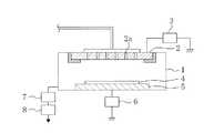
図1は二周波型容量結合プラズマを用いるエッチング装置の概略断面構造を示しており、図1に示すように、反応室1の上部には、エッチングガスを導入するためのガス導入口2aを有する上部電極2が設けられ、該上部電極2には第1の高周波電源3から第1の高周波電力が供給される。反応室1の下部にはシリコン基板4を保持する試料台となる下部電極5が設けられ、該下部電極5には第2の高周波電源6から第2の高周波電力が供給される。また、反応室1の壁部には、反応室1の内部を減圧するターボ分子ポンプ7及びドライポンプ8が接続されている。
【0036】
ターボ分子ポンプ7及びドライポンプ8を駆動して反応室1の内部を所定の圧力に減圧しておいてから、ガス導入口2aから反応室1の内部にエッチングガスを導入すると共に第1の高周波電源3から上部電極2に第1の高周波電力を供給すると、反応室1の内部において、エッチングガスからなるプラズマが発生する。
【0037】
次に、第2の高周波電源6から下部電極5に第2の高周波電力を供給すると、エッチングガスからなるプラズマがシリコン基板4の表面に引き込まれるので、シリコン基板4はエッチングされる。
【0038】
尚、エッチング装置に用いるプラズマとしては、二周波型容量結合プラズマに限らず、容量結合プラズマ、誘導結合プラズマ、マイクロ波プラズマ又はVHFプラズマ等を用いることができる。
【0039】
(第1の実施形態)
以下、第1の実施形態に係るエッチング方法について図面を参照しながら説明する。
【0040】
まず、図2(a)に示すように、ソース領域又はドレイン領域の上にコバルトシリサイド層11が形成されているシリコン基板10の上にゲート絶縁膜12を介して、ポリシリコン膜よりなり高さが250nmで幅が200nmのゲート配線13を形成する。次に、ゲート配線13を含むシリコン基板10の上に、30nmの厚さを持つシリコン窒化膜14と700nmの厚さを持つBPSG膜よりなるシリコン酸化膜15を順次形成した後、該シリコン酸化膜15の上に、200nmのサイズのホール形成用開口部を有するレジストパターン16を形成する。
【0041】
<シリコン酸化膜に対するエッチング工程>
次に、図2(b)に示すように、CH2F2ガスの流量のCH2F2ガスとC5F8ガスとの合計流量に対する比(=CH2F2ガスの混合比)が20%以上であるエッチングガス、例えばCH2F2ガス(流量:5ml/min(標準状態))とC5F8ガス(流量:8ml/min(標準状態))とArガス(流量:800ml/min(標準状態))O2ガス(流量:4ml/min(標準状態))との混合ガスよりなるエッチングガスを用いて、シリコン酸化膜15に対してセルフアラインコンタクトエッチングを行なって、コンタクトホール17を形成する。
【0042】
第1の実施形態によると、エッチングガス中に、堆積膜を成長させる程度が強いC5F8ガスのほかに、シリコン酸化膜に対するエッチングの進行を堆積膜の成長よりも優先させるCH2F2ガスが含まれているため、コンタクトホール17の壁部に付着する堆積膜の成長と、コンタクトホール17の底部に対するエッチングの進行とがバランス良く進行する。このため、コンタクトホール17の底部に堆積膜が付着してエッチングがストップする事態を防止することができる。以下、その理由について次の化学反応式を参照しながら説明する。
【0043】
フルオロカーボンガスにC5F8ガスのみが含まれている場合には、
C5F8+SiO2→SiF4↑+2CO↑+C3F4↑……(1) の化学反応が起こる。
【0044】
これに対して、フルオロカーボンガスにC5F8ガス及びCH2F2ガスが含まれている場合には、
C5F8+CH2F2+SiO2→SiF4↑+2CO↑+C3F6↑+CH2↑……(2)の化学反応が起こる。
【0045】
すなわち、(1) の化学反応が起こる場合には、反応生成物としてC3F4(C/F=0.75)が生成される一方、(2) の化学反応が起こる場合には、反応生成物としてC3F6(C/F=0.50)が生成される。C3F6のC/F比はC3F4のC/F比よりも小さいため、堆積膜の付着が抑制されるので、コンタクトホール17の底部に堆積膜が付着してエッチングがストップする事態を防止することができる。
【0046】
特に、第1の実施形態においては、CH2F2ガスの混合比が20%以上であるエッチングガスを用いるため、シリコン酸化膜15におけるコンタクトホール17の底部に対するエッチングがストップする事態を確実に阻止することができる。以下、その理由について、図3(a)〜(c)を参照しながら説明する。
【0047】
図3(a)は、CH2F2ガスの混合比と、フッ素(F:685nm)の発光強度及び炭素(C2:516nm)の発光強度との関係を示し、図3(b)は、CH2F2ガスの混合比と、C2の発光強度/Fの発光強度(=発光強度比)との関係を示し、図3(c)は、CH2F2ガスの混合比と、コンタクトホールの歩留まりとの関係を示している。
【0048】
図3(a)に示すように、CH2F2ガスの混合比が大きくなっていくと、フルオロカーボンガス中のCH2F2ガスの割合が増加するため、フッ素の発光強度は増大していく。また、CH2F2ガスに含まれる水素によるフッ素のスカベンジ効果により、CH2F2ガスの混合比の増大に伴って、炭素の発光強度も増大していくが、フッ素の発光強度の増大の程度は炭素の発光強度の増大の程度よりも大きい。
【0049】
このため、図3(b)に示すように、CH2F2ガスの混合比が増大するに伴って発光強度比は小さくなっていく。そして、CH2F2ガスの混合比が20%未満では、CH2F2ガスの混合比の増加に伴って発光強度比は急激に小さくなるが、CH2F2ガスの混合比が20%以上になると、発光強度比の低減割合は鈍化していく。このことから、CH2F2ガスの混合比が20%以上になると、プラズマ中の炭素イオンの濃度が確実に低下することが分かる。
【0050】
従って、CH2F2ガスの混合比が20%以上になると、コンタクトホール17の底部に付着する堆積膜が確実に低減するので、図3(c)に示すように、コンタクトホールの歩留まりが急激に向上する。
【0051】
<シリコン窒化膜に対するエッチング工程>
以下、コンタクトホール17の底部に露出したシリコン窒化膜14に対するエッチング工程について説明する。
【0052】
前述のエッチングガス、すなわち、CH2F2ガス及びC5F8ガスを含み且つCH2F2ガスの混合比が20%以上で且つ50%未満であるエッチングガス、例えば、フルオロカーボンガスとして、流量が8ml/min(標準状態)のC5F8ガスと、流量が2〜8ml/min(標準状態)のCH2F2ガスとを含むエッチングガスを用いてエッチングを行なうと、シリコン酸化膜15に対しては確実にエッチングが行なわれ、良好なコンタクトホール17を形成することはできるが、コンタクトホール17の底部に露出したシリコン窒化膜14に対してはエッチングは殆ど行なわれない。
【0053】
そこで、シリコン窒化膜14に対するエッチング選択性に優れるエッチングガス、例えばフルオロカーボンガスとしてCHF3ガスを含むエッチングガスを用いて、コンタクトホール17の底部に露出したシリコン窒化膜14に対してエッチングを行なう。
【0054】
ところが、このエッチングガスはシリコン窒化膜14に対するエッチング選択性に優れるため、図4(a)に示すように、シリコン窒化膜14の角部(ゲート配線13の肩部)がエッチングされてしまい、ゲート配線13がコンタクトホール17に露出するという問題が起きる。
【0055】
そこで、CH2F2ガス及びC5F8ガスを含み且つCH2F2ガスの混合比が50%以上で且つ70%以下であるエッチングガス、例えばフルオロカーボンガスとして、流量が8ml/min(標準状態)のC5F8ガスと流量が8〜18ml/min(標準状態)のCH2F2ガスとを含むエッチングガスを用いて、シリコン酸化膜15に対してエッチングを行なう。
【0056】
このようにすると、シリコン酸化膜15に対して確実にエッチングが行なわれ良好なコンタクトホール17を形成できると共に、引き続き、コンタクトホール17の底部に露出したシリコン窒化膜14に対してエッチングが行なわれ、図4(b)に示すように、シリコン窒化膜14の角部をエッチングすることなく、コバルトシリサイド層11を露出させることができる。
【0057】
一方、CH2F2ガス及びC5F8ガスを含み且つCH2F2ガスの混合比が70%を超えるエッチングガス、例えばフルオロカーボンガスとして、流量が8ml/min(標準状態)のC5F8ガスと流量が18ml/min(標準状態)よりも多いCH2F2ガスとを含むエッチングガスを用いて、シリコン酸化膜15に対してエッチングを行なうと、次のようになる。
【0058】
シリコン酸化膜15に対して確実にエッチングが行なわれ、良好なコンタクトホール17を形成でき、引き続き、コンタクトホール17の底部に露出したシリコン窒化膜14に対してエッチングが行なわれるので、コバルトシリサイド層11を露出させることができる。
【0059】
ところが、CH2F2ガスの混合比が70%を超えるため、シリコン窒化膜14に対するエッチング選択性が大きくなり、図4(c)に示すように、シリコン窒化膜14の角部(ゲート配線13の肩部)がエッチングされてしまい、ゲート配線13がコンタクトホール17に露出するという問題が起きる。
【0060】
従って、CH2F2ガス及びC5F8ガスを含み且つCH2F2ガスの混合比が50%以上で且つ70%以下であるエッチングガスを用いることが最も好ましい。
【0061】
以下、CH2F2ガスの混合比を変化させたときのエッチングモデルについて図5(a)〜(d)を参照しながら説明する。
【0062】
図5(a)は、コンタクトホール17の底部に露出したシリコン窒化膜14に対してエッチングが行なわれる前の状態を示している。図5(a)において、コンタクトホール17におけるシリコン窒化膜14よりも上側部分のサイズaは200nmであり、コンタクトホール17におけるシリコン窒化膜14よりも下側部分のサイズbは100〜150nmである。
【0063】
図5(b)は、CH2F2ガスの混合比が0よりも大きく且つ50%未満であるときのモデルを示し、図5(c)は、CH2F2ガスの混合比が50%以上且つ70%以下であるときのモデルを示し、図5(d)は、CH2F2ガスの混合比が70%よりも多いときのモデルを示している。
【0064】
CH2F2ガスの混合比が0よりも大きく且つ50%未満である場合には、図5(b)に示すように、シリコン窒化膜14におけるゲート配線13の角部と対応する部位及びコンタクトホール17の底部にCxFyよりなる堆積膜が多く付着するので、フッ素によるシリコン窒化膜14に対するエッチングが防止される。
【0065】
CH2F2ガスの混合比が50%以上且つ70%以下である場合には、図5(c)に示すように、シリコン窒化膜14におけるゲート配線13の角部と対応する部位にCxFyよりなる堆積膜が多く付着する一方、コンタクトホール17の底部にはCxFyよりなる堆積膜が少なく付着する。その理由は、シリコン窒化膜14におけるゲート配線13の角部と対応する部位は、ホールサイズa(=200nm)が大きく面積も大きいためプラズマに曝され易い一方、コンタクトホール17の底部は、ホールサイズb(=100〜150nm)が小さく面積も小さいためプラズマに曝され難いからである。従って、フッ素イオンがシリコン窒化膜14におけるコンタクトホール17の底部に照射するので、コンタクトホール17の底部に対するエッチングは進行する。
【0066】
CH2F2ガスの混合比が70%を超える場合には、図5(d)に示すように、シリコン窒化膜14におけるゲート配線13の角部と対応する部位及びコンタクトホール17の底部では、CxFyよりなる堆積膜が殆ど付着しないため、フッ素イオンによるシリコン窒化膜14に対するエッチングが進行する。
【0067】
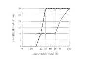
図6は、CH2F2ガスの混合比とシリコン窒化膜14のエッチング量との関係を示している。図6において、○はシリコン窒化膜14におけるゲート配線13の角部と対応する部位のエッチング量を示し、△はシリコン窒化膜14におけるコンタクトホール17の底部のエッチング量を示している。図6から分かるように、CH2F2ガスの混合比が70%を超えると、シリコン窒化膜14におけるゲート配線13の角部と対応する部位のエッチング量が急激に増加し、またCH2F2ガスの混合比が50%未満になると、シリコン窒化膜14におけるコンタクトホール17の底部のエッチング量が急激に減少する。
【0068】
図7は、CH2F2ガスの混合比と、リーク電流の非発生率(△で示す)及びコンタクト抵抗の歩留まり率(○で示す)との関係を示している。リーク電流の非発生率が0%であるということはゲート配線13とコンタクトホール17に埋め込まれた導電膜とがショートしてリーク電流が流れることを意味し、リーク電流の非発生率が100%であるということはゲート配線13とコンタクトホール17に埋め込まれた導電膜とが接触せずリーク電流が流れず正常であることを意味する。また、コンタクト抵抗の歩留まり率が0%であるということはコバルトシリサイド層11とコンタクトホール17に埋め込まれた導電膜とが接触しておらず抵抗値が無限大であることを意味し、コンタクト抵抗の歩留まり率が100%であるということはコバルトシリサイド層11とコンタクトホール17に埋め込まれた導電膜とが確実に接触しており抵抗値が正常であることを意味する。
【0069】
リーク電流の非発生率が100%であり且つコンタクト抵抗の歩留まり率が100%であることが、デバイスが良品であるための条件であると言える。従って、CH2F2ガスの混合比が50%以上で且つ70%以下であるエッチングガスを用いると、良品なデバイスを得られることが分かる。
【0070】
以上の説明から分かるように、コンタクトホール17の底部に露出したシリコン窒化膜14に対するエッチング工程においては、CH2F2ガス及びC5F8ガスを含み且つCH2F2ガスの混合比が50%以上で且つ70%以下であるエッチングガスを用いると、シリコン窒化膜14におけるゲート電極13の角部と対応する部位が過度にエッチングされないため、ゲート配線13とコンタクトホール17に埋め込まれた導電膜とが接触せず、また、シリコン窒化膜14におけるコンタクトホール17の底部が確実にエッチングされて、コバルトシリサイド層11とコンタクトホール17に埋め込まれた導電膜とが確実に接触する。
【0071】
(第2の実施形態)
以下、第2の実施形態に係るエッチング方法について図面を参照しながら説明する。
【0072】
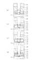
まず、図8(a)に示すように、ソース領域又はドレイン領域の上にコバルトシリサイド層21が形成されているシリコン基板20の上にゲート絶縁膜22を介して、ポリシリコン膜よりなり高さが250nmで幅が200nmのゲート配線23を形成した後、ゲート配線23を含むシリコン基板20の上に、ゲート配線23同士の間に凹部を有し且つ30nmの厚さを持つシリコン窒化膜24を堆積する。
【0073】
次に、シリコン窒化膜24の上に、3.9wt%のボロン及び7.0wt%のリンを含み且つ350nmの厚さを持つBPSG膜よりなる下層の層間絶縁膜25をシリコン窒化膜24の凹部が充填されるように形成した後、CMP法により下層の層間絶縁膜25を平坦化し、その後、平坦化された下層の層間絶縁膜25の上にプラズマCVD法により、不純物を実質的に含まず且つ350nmの厚さを持つシリコン酸化膜よりなる上層の層間絶縁膜26を形成する。
【0074】
次に、上層の層間絶縁膜26の上に、サイズが200nmのホール形成用開口部を有するレジストパターン27を形成する。
【0075】
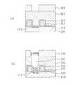
次に、上層の層間絶縁膜26に対して、Arガスと、O2ガスと、C5F8ガスとの混合ガスよりなりO2ガスのフルオロカーボンガスに対する混合割合が相対的に大きい第1のエッチングガス、例えば、流量が800ml/min(標準状態)のArガスと、流量が35ml/min(標準状態)のO2ガスと、流量が15ml/min(標準状態)のC5F8ガスとの混合ガスよりなる第1のエッチングガスを用いてプラズマエッチングを行なって、図8(b)に示すように、上層の層間絶縁膜26にコンタクトホール28の上部28aを形成する。
【0076】
次に、下層の層間絶縁膜26に対して、Arガスと、O2ガスと、C5F8ガスと、CH2F2ガスとの混合ガスよりなりO2ガスのフルオロカーボンガスに対する混合割合が相対的に小さい第2のエッチングガス、例えば、流量が800ml/min(標準状態)のArガスと、流量が4ml/min(標準状態)のO2ガスと、流量が8ml/min(標準状態)のC5F8ガスと、流量が5ml/min(標準状態)のCH2F2ガスとの混合ガスよりなる第2のエッチングガスを用いてセルフアラインコンタクトエッチングを行なって、図8(b)に示すように、下層の層間絶縁膜25にコンタクトホール28の下部28bを形成する。
【0077】
第2の実施形態においては、不純物を実質的に含まないシリコン酸化膜よりなる上層の層間絶縁膜26に対して、Arガスと、O2ガスと、C5F8ガスとの混合ガスよりなりO2ガスのフルオロカーボンガスに対する混合割合が相対的に大きい第1のエッチングガスを用いて第1段階のプラズマエッチングを行なうため、ほぼ垂直な形状を有するコンタクトホール28の上部28aを形成することができる。
【0078】
この場合、第1のエッチングガスにおける、O2ガスの流量のO2ガスとC5F8ガスとの合計流量の比(=O2ガスの混合比)としては60%以上が好ましい。このようにすると、トップサイズ及びボトムサイズがいずれも200nmであり、ほぼ垂直な形状を有するコンタクトホール28の上部28aを確実に形成することができる。
【0079】
また、BPSG膜よりなる下層の層間絶縁膜26に対して、Arガスと、O2ガスと、C5F8ガスと、CH2F2ガスとの混合ガスよりなりO2ガスのフルオロカーボンガスに対する混合割合が相対的に小さい第2のエッチングガスを用いて第2段階のプラズマエッチングを行なうため、すなわち、O2ガスのフルオロカーボンガスに対する混合割合が相対的に小さいため、シリコン窒化膜24におけるコンタクトホール28の壁部が過度にエッチングされないと共に、第2のエッチングガスにCH2F2ガスが混合されているため、エッチングが停止することなくコンタクトホール28の下部28bを形成することができる。
【0080】
この場合、第1の実施形態と同様の理由により、第2のエッチングガスにおけるCH2F2ガスの混合比が20%以上であると、コンタクトホール28の底部に堆積膜が付着してエッチングがストップする事態を確実に阻止することができる。また、第2のエッチングガスにおけるCH2F2ガスの混合比が50%以上であると、下層の層間絶縁膜26に対するエッチングに引き続いて、シリコン窒化膜24におけるコンタクトホール28の底部をエッチングすることができる。また、第2のエッチングガスにおけるCH2F2ガスの混合比が50%以上で且つ70%以下であると、シリコン窒化膜24におけるゲート配線23の肩部と対応する部位が過度にエッチングされることなく、シリコン窒化膜24におけるコンタクトホール28の底部をエッチングすることができる。
【0081】
以上の理由により、第2の実施形態においては、第2のエッチングガスにおけるCH2F2ガスの混合比としては、20%以上で且つ70%以下であることが好ましい。
【0082】
このようにすると、図8(b)に示すように、トップサイズ及びボトムサイズがいずれも200nmであるコンタクトホール28の上部28aを形成することができると共に、トップサイズが200nmで且つボトムサイズが150nmであるコンタクトホール28の下部28bを形成することができる。すなわち、トップサイズが200nmでボトムサイズが150nmであるコンタクトホール28を形成することができる。
【0083】
第2の実施形態においては、下層の層間絶縁膜25として、3.9wt%のボロン及び7.0wt%のリンを含み、流動性に優れたBPSG膜を用いているため、下層の層間絶縁膜25をシリコン窒化膜24の凹部に確実に充填することができる。
【0084】
また、上層の層間絶縁膜26として、不純物を実質的に含まないシリコン酸化膜を用いているため、上層の層間絶縁膜26にコンタクトホール28の上部28aを形成するためのエッチング工程において、シリコン窒化膜24がエッチングされてゲート配線23が露出してしまう事態を回避できる。すなわち、CMP法により下層の層間絶縁膜25を平坦化した後には、下層の層間絶縁膜25におけるゲート配線23の上側部分の厚さは小さくなっている。このため、上層の層間絶縁膜26としてBPSG膜を用いると共に、ほぼ垂直な形状を有するコンタクトホール28の上部28aを形成するべく、O2ガスの混合比が60%以上であるエッチングガスを用いると、BPSG膜に対するエッチングのシリコン窒化膜24に対するエッチングの選択性が低くなってしまうので、シリコン窒化膜24がエッチングされてゲート配線23が露出してしまう恐れがある。ところが、上層の層間絶縁膜26として不純物を実質的に含まないシリコン酸化膜を用いているため、上層の層間絶縁膜26にコンタクトホール28の上部28aを形成するためのエッチング工程において、シリコン窒化膜24は殆どエッチングされない。
【0085】
次に、酸素プラズマを用いるアッシングにより、図8(c)に示すように、レジストパターン27とコンタクトホール28の内部に残存しているポリマー膜を除去した後、フッ酸を含む水溶液を用いるウェットエッチングにより、図8(d)に示すように、コンタクトホール27の内部に残存する下層の層間絶縁膜25を除去する。
【0086】
このウェットエッチング工程においては、不純物を含まないシリコン酸化膜よりなる緻密な上層の層間絶縁膜25はフッ酸溶液によりエッチングされない一方、ボロン及びリンの濃度が高いBPSG膜よりなる下層の層間絶縁膜26はフッ酸溶液によりエッチングされるため、コンタクトホール27の内部に残存する下層の層間絶縁膜25を確実に除去される。
【0087】
このため、コンタクトホール27のボトムサイズは拡大して170nmになるので、コンタクト抵抗の低減を図ることができる。
【0088】
以下、第2の実施形態に係るエッチング方法を評価するために行なった比較例について、図10(a)、(b)を参照しながら説明する。
【0089】
まず、図10(a)に示すように、第2の実施形態と同様に、コバルトシリサイド層111が形成されているシリコン基板110の上にゲート絶縁膜112を介して、ポリシリコン膜よりなり高さが250nmで幅が200nmのゲート配線113を形成した後、ゲート配線113を含むシリコン基板110の上にシリコン窒化膜114を堆積する。その後、シリコン窒化膜114の上に、3.9wt%のボロン及び7.0wt%のリンを含み且つ700nmの厚さを持つBPSG膜よりなる層間絶縁膜115を形成する。
【0090】
次に、層間絶縁膜115に対して、流量が800ml/min(標準状態)のArガスと、流量が4ml/min(標準状態)のO2ガスと、流量が8ml/min(標準状態)のC5F8ガスと、流量が5ml/min(標準状態)のCH2F2ガスとの混合ガスよりなるエッチングガスを用いてプラズマエッチングを行なって、層間絶縁膜115にコンタクトホール117を形成する。
【0091】
比較例によると、図10(b)に示すように、コンタクトホール117の形状は、テーパ角が85°以下のテーパ形状になり、トップサイズが200nmであるのに対してボトムサイズは100nmになる。このように、コンタクトホール117のボトムサイズが小さくなるので、コンタクト抵抗が大きくなる。この場合、コンタクトホール117とゲート配線113同士の間の凹部とのアライメントずれが大きくなると、コンタクトホール117のボトムサイズは一層小さくなってしまう。
【0092】
【発明の効果】
第1のエッチング方法によると、凹部の壁部に付着する堆積膜の成長と、凹部の底部に対するエッチングの進行とがバランス良く進行するため、凹部の底部に堆積膜が付着してエッチングがストップする事態を防止することができる。
【0093】
第2のエッチング方法によると、上層膜にほぼ垂直な形状を有する凹部の上部を形成することができ、凹部に露出しているシリコン窒化膜の側壁部が過度にエッチングされず、下層膜にエッチングの停止を招くことなく凹部の下部を形成することができる。
【0094】
第3のエッチング方法によると、上層膜にほぼ垂直な形状を有する第2の凹部の上部を形成することができ、第1の凹部に露出しているシリコン窒化膜の側壁部が過度にエッチングされず、下層膜にエッチングの停止を招くことなく第2の凹部の下部を形成することができる。
【図面の簡単な説明】
【図1】本発明の各実施形態に係るエッチング方法に用いるエッチング装置の断面図である。
【図2】(a)、(b)は本発明の第1の実施形態に係るエッチング方法の各工程を示す断面図である。
【図3】(a)は、CH2F2ガスの混合比と、フッ素の発光強度及び炭素の発光強度との関係を示す図であり、(b)は、CH2F2ガスの混合比と、C2の発光強度/Fの発光強度との関係を示す図であり、(c)は、CH2F2ガスの混合比と、コンタクトホールの歩留まりとの関係を示す図である。
【図4】(a)〜(c)は、本発明の第1の実施形態に係るエッチング方法において、シリコン窒化膜におけるコンタクトホールの底部に対するエッチング工程を説明する断面図である。
【図5】(a)〜(d)は、本発明の第1の実施形態に係るエッチング方法において、CH2F2ガスの混合比を変化させたときのエッチングモデルを説明する断面図である。
【図6】本発明の第1の実施形態に係るエッチング方法において、CH2F2ガスの混合比とシリコン窒化膜のエッチング量との関係を示す図である。
【図7】本発明の第1の実施形態に係るエッチング方法において、CH2F2ガスの混合比と、リーク電流の非発生率及びコンタクト抵抗の歩留まり率との関係を示す図である。
【図8】(a)〜(c)は本発明の第2の実施形態に係るエッチング方法の各工程を示す断面図である。
【図9】(a)、(b)は従来のエッチング方法の各工程を示す断面図である。
【図10】(a)、(b)は第2の実施形態の比較例に係るエッチング方法の各工程を示す断面図である。
【符号の説明】
10 シリコン基板
11 コバルトシリサイド層
12 ゲート絶縁膜
13 ゲート配線
14 シリコン窒化膜
15 シリコン酸化膜
16 レジストパターン
17 コンタクトホール
20 シリコン基板
21 コバルトシリサイド層
22 ゲート絶縁膜
23 ゲート配線
24 シリコン窒化膜
25 下層の層間絶縁膜
26 上層の層間絶縁膜
27 レジストパターン
28 コンタクトホール
28a コンタクトホールの上部
28b コンタクトホールの下部[0001]
[Technical field to which the invention belongs]
The present invention relates to an etching method for forming a recess having a high aspect ratio in a silicon oxide film formed on a substrate via a silicon nitride film.
[0002]
[Prior art]
As the size of semiconductor devices is reduced, the amount of misalignment between masks has become a value that cannot be ignored. For example, if the mask misalignment between the gate wiring and the contact hole is large, there is a problem that the gate wiring and the conductive film embedded in the contact hole are short-circuited and the device does not operate.
[0003]
Therefore, an etching method called a self-aligned contact etching method has been proposed. Hereinafter, this etching method will be described with reference to FIG.
[0004]
As shown in FIG. 9A, a gate wiring (gate electrode) made of a polysilicon film via a gate
[0005]
Plasma etching is performed on the
[0006]
By the way, since it is necessary to remove the
[0007]
Further, after removing the
[0008]
Therefore, an etching gas containing a fluorocarbon gas, such as Ar gas and O, is applied to the
[0009]
[Problems to be solved by the invention]
For the
[0010]
However, as the aspect ratio of the
[0011]
In view of the above, the present invention forms a recess having a high aspect ratio in the silicon oxide film by etching the silicon oxide film formed on the silicon nitride film using an etching gas containing a fluorocarbon gas. At this time, it is an object to prevent the etching of the bottom of the recess in the silicon oxide film from stopping.
[0012]
[Means for Solving the Problems]
In order to achieve the above object, a first etching method according to the present invention is directed to an etching method for forming a recess having a high aspect ratio in a silicon oxide film formed on a substrate via a silicon nitride film. Ar gas and O2 Gas and CFive F8 Gas and CH2 F2 An etching gas made of a mixed gas with a gas is used.
[0013]
According to the first etching method, there is a strong tendency to grow a deposited film on the wall of the recess in the etching gas.Five F8 In addition to the gas, the etching progress to the bottom of the recess is prioritized over the growth of the deposited film on the wall of the recess.2 F2 Since the gas is contained, the growth of the deposited film on the wall portion of the recess and the progress of the etching on the bottom portion of the recess proceed in a balanced manner. For this reason, the situation where the etching with respect to the bottom part of the recessed part in a silicon oxide film stops can be prevented.
[0014]
In the first etching method, CH contained in the etching gas2 F2 C of gas flow rateFive F8 Gas and CH2 F2 The ratio with respect to the total flow rate with the gas is preferably 20% or more.
[0015]
In this way, it is possible to reliably avoid the situation where the etching on the bottom of the recess in the silicon oxide film stops.
[0016]
In the first etching method, CH contained in the etching gas2 F2 C of gas flow rateFive F8 Gas and CH2 F2 The ratio of the total flow rate with the gas is preferably 50% or more.
[0017]
In this way, after the recess is formed in the silicon oxide film, the silicon nitride film exposed at the bottom of the recess can be continuously etched.
[0018]
In the first etching method, CH contained in the etching gas2 F2 C of gas flow rateFive F8 Gas and CH2 F2 The ratio with respect to the total flow rate with the gas is preferably 50% or more and 70% or less.
[0019]
Thus, when the silicon nitride film is exposed at the wall portion of the recess, the silicon nitride film exposed at the bottom of the recess can be etched without etching the corner portion of the silicon nitride film.
[0020]
A second etching method according to the present invention includes a lower layer film made of a silicon oxide film containing impurities and an upper layer film made of a silicon oxide film substantially free of impurities formed on a substrate via a silicon nitride film. An etching method for forming a recess having a high aspect ratio in a laminated film is formed, and Ar gas and O2 Gas and CFive F8 It consists of a gas mixture with gas, and O2 A step of performing a first stage etching using a first etching gas having a relatively high mixing ratio of the gas to the fluorocarbon gas, and Ar gas and O2 Gas and CFive F8 Gas and CH2 F2 It consists of a gas mixture with gas, and O2 And a second step of etching using a second etching gas having a relatively low mixing ratio of the gas to the fluorocarbon gas.
[0021]
According to the second etching method, Ar gas and
[0022]
In the second etching method, CH contained in the second etching gas2 F2 C of gas flow rateFive F8 Gas and CH2 F2 The ratio with respect to the total flow rate with the gas is preferably 20% or more.
[0023]
In this way, it is possible to reliably avoid the situation where the etching on the bottom of the recess in the silicon oxide film stops.
[0024]
In the second etching method, CH contained in the second etching gas2 F2 C of gas flow rateFive F8 Gas and CH2 F2 The ratio of the total flow rate with the gas is preferably 50% or more.
[0025]
In this way, after the recess is formed in the silicon oxide film, the silicon nitride film exposed at the bottom of the recess can be continuously etched.
[0026]
In the second etching method, CH contained in the second etching gas2 F2 C of gas flow rateFive F8 Gas and CH2 F2 The ratio with respect to the total flow rate with the gas is preferably 50% or more and 70% or less.
[0027]
Thus, when the silicon nitride film is exposed at the wall portion of the recess, the silicon nitride film exposed at the bottom of the recess can be etched without etching the corner portion of the silicon nitride film.
[0028]
According to a third etching method of the present invention, a silicon nitride film formed on a substrate and formed on a silicon nitride film having a first recess and made of a silicon oxide film containing impurities and silicon substantially free of impurities. An etching method for forming a second concave portion integrated with the first concave portion and having a high aspect ratio in a laminated film composed of an upper layer film made of an oxide film, and with respect to the upper layer film, Ar gas and , O2 Gas and CFive F8 It consists of a gas mixture with gas, and O2 A step of performing a first-stage dry etching using a first etching gas having a relatively high mixing ratio of the gas to the fluorocarbon gas, and Ar gas and O2 Gas and CFive F8 Gas and CH2 F2 It consists of a gas mixture with gas, and O2 A step of performing a second stage dry etching using a second etching gas having a relatively low mixing ratio of the gas to the fluorocarbon gas, and a step of removing the lower layer film remaining in the first recess by wet etching. I have.
[0029]
According to the third etching method, similarly to the second etching method, the upper portion of the second recess having a shape substantially perpendicular to the upper layer film can be formed, and the silicon nitride film exposed in the first recess is exposed. The side wall portion of the second recess is not excessively etched, and the lower portion of the second recess can be formed without causing etching to stop in the lower layer film.
[0030]
In the third etching method, CH contained in the second etching gas2 F2 C of gas flow rateFive F8 Gas and CH2 F2 The ratio with respect to the total flow rate with the gas is preferably 20% or more and 70% or less.
[0031]
In this way, the second recess having a large taper angle and a shape close to vertical can be formed.
[0032]
In the third etching method, the lower layer film is preferably a BPSG film containing 3.7 wt% boron and 7.0 wt% phosphorus.
[0033]
Since the BPSG film having such a composition is excellent in fluidity, the lower film made of the BPSG film is surely filled into the first recess formed in the silicon nitride film.
[0034]
DETAILED DESCRIPTION OF THE INVENTION
(Etching device)
Hereinafter, an etching method according to each embodiment of the present invention will be described. As a premise thereof, an etching apparatus used for the etching method according to each embodiment of the present invention will be described with reference to FIG.
[0035]
FIG. 1 shows a schematic cross-sectional structure of an etching apparatus using a dual frequency capacitively coupled plasma. As shown in FIG. 1, a
[0036]
After the turbo
[0037]
Next, when the second high frequency power is supplied from the second high frequency power source 6 to the lower electrode 5, the plasma made of the etching gas is drawn into the surface of the silicon substrate 4, so that the silicon substrate 4 is etched.
[0038]
Note that the plasma used in the etching apparatus is not limited to the dual-frequency capacitively coupled plasma, and capacitively coupled plasma, inductively coupled plasma, microwave plasma, VHF plasma, or the like can be used.
[0039]
(First embodiment)
Hereinafter, the etching method according to the first embodiment will be described with reference to the drawings.
[0040]
First, as shown in FIG. 2A, the height is made of a polysilicon film via a
[0041]
<Etching process for silicon oxide film>
Next, as shown in FIG.2 F2 Gas flow rate CH2 F2 Gas and CFive F8 Ratio to total flow rate with gas (= CH2 F2 Etching gas whose gas mixing ratio is 20% or more, for example CH2 F2 Gas (flow rate: 5 ml / min (standard state)) and CFive F8 Gas (flow rate: 8 ml / min (standard state)) and Ar gas (flow rate: 800 ml / min (standard state)) O2
[0042]
According to the first embodiment, the degree of growth of the deposited film is strong in the etching gas.Five F8 In addition to the gas, the etching process for the silicon oxide film has priority over the growth of the deposited film2 F2 Since the gas is contained, the growth of the deposited film adhering to the wall portion of the
[0043]
C for fluorocarbon gasFive F8 If only gas is included,
CFive F8 + SiO2 → SiFFour ↑ + 2CO ↑ + CThree FFour ↑ …… (1) chemical reaction occurs.
[0044]
In contrast, C is added to the fluorocarbon gas.Five F8 Gas and CH2 F2 If gas is included,
CFive F8 + CH2 F2 + SiO2 → SiFFour ↑ + 2CO ↑ + CThree F6 ↑ + CH2 ↑ …… (2) chemical reaction occurs.
[0045]
That is, when the chemical reaction (1) occurs, the reaction product is CThree FFour (C / F = 0.75) is produced, but when the chemical reaction of (2) occurs, C as the reaction productThree F6 (C / F = 0.50) is generated. CThree F6 The C / F ratio is CThree FFour Since the C / F ratio is smaller than this, adhesion of the deposited film is suppressed, so that the situation where the deposited film adheres to the bottom of the
[0046]
In particular, in the first embodiment, CH2 F2 Since an etching gas having a gas mixing ratio of 20% or more is used, it is possible to reliably prevent the etching of the bottom portion of the
[0047]
FIG. 3 (a) shows the CH2 F2 Mixing ratio of gas, emission intensity of fluorine (F: 685 nm) and carbon (C2 : 516 nm), and FIG.2 F2 Gas mixing ratio and C2 FIG. 3 (c) shows the relationship between the emission intensity of F / the emission intensity of F and the emission intensity ratio (= emission intensity ratio).2 F2 The relationship between the gas mixture ratio and the contact hole yield is shown.
[0048]
As shown in FIG.2 F2 As the gas mixing ratio increases, CH in the fluorocarbon gas2 F2 As the gas ratio increases, the emission intensity of fluorine increases. CH2 F2 Due to the scavenging effect of fluorine by hydrogen contained in the gas, CH2 F2 As the gas mixture ratio increases, the emission intensity of carbon also increases, but the increase in the emission intensity of fluorine is greater than the increase in the emission intensity of carbon.
[0049]
For this reason, as shown in FIG.2 F2 As the gas mixture ratio increases, the emission intensity ratio decreases. And CH2 F2 When the gas mixture ratio is less than 20%, CH2 F2 As the gas mixture ratio increases, the emission intensity ratio decreases rapidly.2 F2 When the gas mixture ratio is 20% or more, the reduction ratio of the light emission intensity ratio decreases. From this, CH2 F2 It can be seen that when the gas mixing ratio is 20% or more, the concentration of carbon ions in the plasma is reliably reduced.
[0050]
Therefore, CH2 F2 When the gas mixing ratio is 20% or more, the deposited film adhering to the bottom of the
[0051]
<Etching process for silicon nitride film>
Hereinafter, an etching process for the
[0052]
The aforementioned etching gas, ie CH2 F2 Gas and CFive F8 Contains gas and CH2 F2 An etching gas having a gas mixing ratio of 20% or more and less than 50%, for example, fluorocarbon gas, C having a flow rate of 8 ml / min (standard state).Five F8 Gas and CH with a flow rate of 2-8 ml / min (standard state)2 F2 When etching is performed using an etching gas containing a gas, the
[0053]
Therefore, an etching gas excellent in etching selectivity with respect to the
[0054]
However, since this etching gas has excellent etching selectivity with respect to the
[0055]
So CH2 F2 Gas and CFive F8 Contains gas and CH2 F2 As an etching gas having a gas mixing ratio of 50% or more and 70% or less, for example, fluorocarbon gas, C having a flow rate of 8 ml / min (standard state).Five F8 CH with gas and flow rate 8-18ml / min (standard state)2 F2 The
[0056]
In this way, the
[0057]
On the other hand, CH2 F2 Gas and CFive F8 Contains gas and CH2 F2 Etching gas with a gas mixture ratio exceeding 70%, for example, fluorocarbon gas, C having a flow rate of 8 ml / min (standard state)Five F8 CH with more gas and flow rate than 18ml / min (standard condition)2 F2 When the
[0058]
Since the
[0059]
However, CH2 F2 Since the gas mixing ratio exceeds 70%, the etching selectivity with respect to the
[0060]
Therefore, CH2 F2 Gas and CFive F8 Contains gas and CH2 F2 It is most preferable to use an etching gas having a gas mixing ratio of 50% or more and 70% or less.
[0061]
CH2 F2 An etching model when the gas mixture ratio is changed will be described with reference to FIGS.
[0062]
FIG. 5A shows a state before the
[0063]
FIG. 5B shows the CH2 F2 FIG. 5 (c) shows a model when the gas mixture ratio is larger than 0 and less than 50%.2 F2 FIG. 5 (d) shows a model when the gas mixing ratio is 50% or more and 70% or less.2 F2 The model is shown when the gas mixing ratio is greater than 70%.
[0064]
CH2 F2 When the gas mixing ratio is greater than 0 and less than 50%, as shown in FIG. 5B, the portion corresponding to the corner of the
[0065]
CH2 F2 When the gas mixture ratio is 50% or more and 70% or less, as shown in FIG. 5C, the portion of the
[0066]
CH2 F2 When the gas mixture ratio exceeds 70%, as shown in FIG. 5D, at the portion corresponding to the corner of the
[0067]
6 shows the CH2 F2 The relationship between the gas mixing ratio and the etching amount of the
[0068]
FIG. 7 shows the CH2 F2 The relationship between the gas mixing ratio, the leakage current non-occurrence rate (indicated by Δ), and the contact resistance yield rate (indicated by ○) is shown. A leakage current non-occurrence rate of 0% means that the leakage current flows due to a short circuit between the
[0069]
It can be said that the non-occurrence rate of the leak current is 100% and the yield rate of the contact resistance is 100% is a condition for the device to be non-defective. Therefore, CH2 F2 It can be seen that a good device can be obtained when an etching gas having a gas mixing ratio of 50% or more and 70% or less is used.
[0070]
As can be seen from the above description, in the etching process for the
[0071]
(Second Embodiment)
Hereinafter, an etching method according to the second embodiment will be described with reference to the drawings.
[0072]
First, as shown in FIG. 8 (a), the height is made of a polysilicon film via a
[0073]
Next, a lower
[0074]
Next, a resist
[0075]
Next, with respect to the upper
[0076]
Next, with respect to the lower
[0077]
In the second embodiment, Ar gas and
[0078]
In this case, O in the first etching gas.2 O of gas flow rate2 Gas and CFive F8 Ratio of total flow rate with gas (= O2 The gas mixing ratio is preferably 60% or more. In this way, the top size and the bottom size are both 200 nm, and the
[0079]
Further, for the lower
[0080]
In this case, CH in the second etching gas for the same reason as in the first embodiment.2 F2 When the gas mixture ratio is 20% or more, it is possible to reliably prevent the situation where the deposited film adheres to the bottom of the
[0081]
For the above reason, in the second embodiment, CH in the second etching gas is used.2 F2 The gas mixing ratio is preferably 20% or more and 70% or less.
[0082]
In this way, as shown in FIG. 8B, it is possible to form the
[0083]
In the second embodiment, since the lower
[0084]
Further, since a silicon oxide film substantially free of impurities is used as the upper
[0085]
Next, as shown in FIG. 8C, the polymer film remaining inside the resist
[0086]
In this wet etching process, the dense upper
[0087]
For this reason, since the bottom size of the
[0088]
Hereinafter, a comparative example performed for evaluating the etching method according to the second embodiment will be described with reference to FIGS.
[0089]
First, as shown in FIG. 10A, as in the second embodiment, a polysilicon film is formed on a
[0090]
Next, with respect to the
[0091]
According to the comparative example, as shown in FIG. 10B, the shape of the
[0092]
【The invention's effect】
According to the first etching method, the growth of the deposited film adhering to the wall portion of the recess and the progress of the etching with respect to the bottom portion of the recess proceed in a balanced manner, so that the deposited film adheres to the bottom portion of the recess and the etching stops. The situation can be prevented.
[0093]
According to the second etching method, the upper portion of the recess having a shape substantially perpendicular to the upper layer film can be formed, and the side wall portion of the silicon nitride film exposed to the recess is not excessively etched and etched into the lower layer film. The lower portion of the recess can be formed without incurring any stoppage.
[0094]
According to the third etching method, the upper portion of the second recess having a shape substantially perpendicular to the upper layer film can be formed, and the side wall portion of the silicon nitride film exposed to the first recess is excessively etched. First, the lower portion of the second recess can be formed without causing etching to stop in the lower layer film.
[Brief description of the drawings]
FIG. 1 is a cross-sectional view of an etching apparatus used in an etching method according to each embodiment of the present invention.
FIGS. 2A and 2B are cross-sectional views showing respective steps of an etching method according to the first embodiment of the present invention.
FIG. 3 (a) shows CH2 F2 It is a figure which shows the relationship between the mixture ratio of gas, the emission intensity of a fluorine, and the emission intensity of carbon, (b) is CH2 F2 Gas mixing ratio and C2 It is a figure which shows the relationship with the emitted light intensity of / F and the emitted light intensity, (c) is CH2 F2 It is a figure which shows the relationship between the mixture ratio of gas, and the yield of a contact hole.
FIGS. 4A to 4C are cross-sectional views illustrating an etching process for a bottom portion of a contact hole in a silicon nitride film in the etching method according to the first embodiment of the present invention.
FIGS. 5 (a) to 5 (d) are diagrams illustrating an etching method according to the first embodiment of the present invention.2 F2 It is sectional drawing explaining the etching model when changing the mixing ratio of gas.
FIG. 6 shows a CH method in the etching method according to the first embodiment of the present invention.2 F2 It is a figure which shows the relationship between the gas mixture ratio and the etching amount of a silicon nitride film.
FIG. 7 shows a CH method in the etching method according to the first embodiment of the present invention.2 F2 It is a figure which shows the relationship between the mixture ratio of gas, the non-occurrence | production rate of leak current, and the yield rate of contact resistance.
FIGS. 8A to 8C are cross-sectional views showing respective steps of an etching method according to a second embodiment of the present invention.
9A and 9B are cross-sectional views showing respective steps of a conventional etching method.
FIGS. 10A and 10B are cross-sectional views showing respective steps of an etching method according to a comparative example of the second embodiment. FIGS.
[Explanation of symbols]
10 Silicon substrate
11 Cobalt silicide layer
12 Gate insulation film
13 Gate wiring
14 Silicon nitride film
15 Silicon oxide film
16 resist pattern
17 Contact hole
20 Silicon substrate
21 Cobalt silicide layer
22 Gate insulation film
23 Gate wiring
24 Silicon nitride film
25 Lower interlayer insulation film
26 Upper interlayer insulating film
27 resist pattern
28 Contact hole
28a Top of contact hole
28b Bottom of contact hole
Claims (11)
Translated fromJapaneseArガスと、O2ガスと、C5F8ガスと、CH2F2ガスとの混合ガスよりなるエッチングガスを用いて、前記シリコン酸化膜及び前記シリコン窒化膜に対して連続してエッチングを行なうことにより、アスペクト比が高い凹部を形成するエッチング工程とを備えていることを特徴とするエッチング方法。Forming a silicon nitride film on the substrate and forming a silicon oxide film on the silicon nitride film; and
Etching is continuously performed on the silicon oxide film and the silicon nitride film by using an etching gas made of a mixed gas ofAr gas, O2gas, C5F8gas, and CH2F2gas. An etching method comprising:an etching step of forming a recess having a high aspect ratio .
前記上層膜に対して、Arガスと、O2ガスと、C5F8ガスとの混合ガスよりなり、O2ガスの流量がフルオロカーボンガスの流量より大きい第1のエッチングガスを用いる第1段階のエッチングを行なう工程と、
前記下層膜に対して、Arガスと、O2ガスと、C5F8ガスと、CH2F2ガスとの混合ガスよりなり、O2ガスの流量がフルオロカーボンガスの流量より小さい第2のエッチングガスを用いる第2段階のエッチングを行なう工程とを備えていることを特徴とするエッチング方法。Formed through a silicon nitride film on the substrate, forming a recess with a high aspect ratio in a laminated film consisting of a lower layer film made of a silicon oxide film containing impurities and an upper layer film made of a silicon oxide film substantially free of impurities An etching method for performing
To the upper layer film, and Ar gas, and O2 gas, becomes a mixed gas of C5 F8 gas, a first stageof the flow rate of O2 gasis used large first etching gasfrom the flow rate of the fluorocarbon gas Etching step,
With respect to the lower film, and Ar gas, and O2 gas, and C5 F8 gas, it becomes a mixed gas of CH2 F2 gas, the O2 gasflow rate is smaller secondthan the flow rate of the fluorocarbon gas And a second step of etching using an etching gas.
前記上層膜に対して、Arガスと、O2ガスと、C5F8ガスとの混合ガスよりなり、O2ガスの流量がフルオロカーボンガスの流量より大きい第1のエッチングガスを用いる第1段階のドライエッチングを行なう工程と、
前記下層膜に対して、Arガスと、O2ガスと、C5F8ガスと、CH2F2ガスとの混合ガスよりなり、O2ガスの流量がフルオロカーボンガスの流量より小さい第2のエッチングガスを用いる第2段階のドライエッチングを行なう工程と、
前記第1の凹部に残存している前記下層膜をウェットエッチングにより除去する工程とを備えていることを特徴とするエッチング方法。A laminated film formed on a silicon nitride film formed on a substrate and having a first recess, and comprising a lower film made of a silicon oxide film containing impurities and an upper film made of a silicon oxide film substantially free of impurities And an etching method for forming a second recess that is integrated with the first recess and has a high aspect ratio,
To the upper layer film, and Ar gas, and O2 gas, becomes a mixed gas of C5 F8 gas, a first stageof the flow rate of O2 gasis used large first etching gasfrom the flow rate of the fluorocarbon gas Performing the dry etching of
With respect to the lower film, and Ar gas, and O2 gas, and C5 F8 gas, it becomes a mixed gas of CH2 F2 gas, the O2 gasflow rate is smaller secondthan theflow rate of the fluorocarbon gas Performing a second stage dry etching using an etching gas;
And a step of removing the lower layer film remaining in the first recess by wet etching.
Priority Applications (3)
| Application Number | Priority Date | Filing Date | Title |
|---|---|---|---|
| JP2001325813AJP3759895B2 (en) | 2001-10-24 | 2001-10-24 | Etching method |
| CNB021473846ACN1285106C (en) | 2001-10-24 | 2002-10-23 | etching method |
| US10/277,725US6939806B2 (en) | 2001-10-24 | 2002-10-23 | Etching memory |
Applications Claiming Priority (1)
| Application Number | Priority Date | Filing Date | Title |
|---|---|---|---|
| JP2001325813AJP3759895B2 (en) | 2001-10-24 | 2001-10-24 | Etching method |
Publications (2)
| Publication Number | Publication Date |
|---|---|
| JP2003133289A JP2003133289A (en) | 2003-05-09 |
| JP3759895B2true JP3759895B2 (en) | 2006-03-29 |
Family
ID=19142305
Family Applications (1)
| Application Number | Title | Priority Date | Filing Date |
|---|---|---|---|
| JP2001325813AExpired - Fee RelatedJP3759895B2 (en) | 2001-10-24 | 2001-10-24 | Etching method |
Country Status (3)
| Country | Link |
|---|---|
| US (1) | US6939806B2 (en) |
| JP (1) | JP3759895B2 (en) |
| CN (1) | CN1285106C (en) |
Cited By (1)
| Publication number | Priority date | Publication date | Assignee | Title |
|---|---|---|---|---|
| US20210175082A1 (en)* | 2019-12-04 | 2021-06-10 | Spts Technologies Limited | Method, Substrate and Apparatus |
Families Citing this family (156)
| Publication number | Priority date | Publication date | Assignee | Title |
|---|---|---|---|---|
| TWI223380B (en)* | 2003-07-14 | 2004-11-01 | Nanya Technology Corp | Semiconductor device and method of fabricating the same |
| US20090065820A1 (en)* | 2007-09-06 | 2009-03-12 | Lu-Yang Kao | Method and structure for simultaneously fabricating selective film and spacer |
| US9324576B2 (en) | 2010-05-27 | 2016-04-26 | Applied Materials, Inc. | Selective etch for silicon films |
| US8741778B2 (en) | 2010-12-14 | 2014-06-03 | Applied Materials, Inc. | Uniform dry etch in two stages |
| US10283321B2 (en) | 2011-01-18 | 2019-05-07 | Applied Materials, Inc. | Semiconductor processing system and methods using capacitively coupled plasma |
| US8771539B2 (en) | 2011-02-22 | 2014-07-08 | Applied Materials, Inc. | Remotely-excited fluorine and water vapor etch |
| US8999856B2 (en) | 2011-03-14 | 2015-04-07 | Applied Materials, Inc. | Methods for etch of sin films |
| US9064815B2 (en) | 2011-03-14 | 2015-06-23 | Applied Materials, Inc. | Methods for etch of metal and metal-oxide films |
| US8771536B2 (en) | 2011-08-01 | 2014-07-08 | Applied Materials, Inc. | Dry-etch for silicon-and-carbon-containing films |
| US8679982B2 (en) | 2011-08-26 | 2014-03-25 | Applied Materials, Inc. | Selective suppression of dry-etch rate of materials containing both silicon and oxygen |
| US8679983B2 (en) | 2011-09-01 | 2014-03-25 | Applied Materials, Inc. | Selective suppression of dry-etch rate of materials containing both silicon and nitrogen |
| US8927390B2 (en) | 2011-09-26 | 2015-01-06 | Applied Materials, Inc. | Intrench profile |
| US8808563B2 (en) | 2011-10-07 | 2014-08-19 | Applied Materials, Inc. | Selective etch of silicon by way of metastable hydrogen termination |
| WO2013070436A1 (en) | 2011-11-08 | 2013-05-16 | Applied Materials, Inc. | Methods of reducing substrate dislocation during gapfill processing |
| US9267739B2 (en) | 2012-07-18 | 2016-02-23 | Applied Materials, Inc. | Pedestal with multi-zone temperature control and multiple purge capabilities |
| US9373517B2 (en) | 2012-08-02 | 2016-06-21 | Applied Materials, Inc. | Semiconductor processing with DC assisted RF power for improved control |
| US9034770B2 (en) | 2012-09-17 | 2015-05-19 | Applied Materials, Inc. | Differential silicon oxide etch |
| US9023734B2 (en) | 2012-09-18 | 2015-05-05 | Applied Materials, Inc. | Radical-component oxide etch |
| US9390937B2 (en) | 2012-09-20 | 2016-07-12 | Applied Materials, Inc. | Silicon-carbon-nitride selective etch |
| US9132436B2 (en) | 2012-09-21 | 2015-09-15 | Applied Materials, Inc. | Chemical control features in wafer process equipment |
| US8765574B2 (en) | 2012-11-09 | 2014-07-01 | Applied Materials, Inc. | Dry etch process |
| US8969212B2 (en) | 2012-11-20 | 2015-03-03 | Applied Materials, Inc. | Dry-etch selectivity |
| US8980763B2 (en) | 2012-11-30 | 2015-03-17 | Applied Materials, Inc. | Dry-etch for selective tungsten removal |
| US9064816B2 (en) | 2012-11-30 | 2015-06-23 | Applied Materials, Inc. | Dry-etch for selective oxidation removal |
| US9111877B2 (en) | 2012-12-18 | 2015-08-18 | Applied Materials, Inc. | Non-local plasma oxide etch |
| US8921234B2 (en) | 2012-12-21 | 2014-12-30 | Applied Materials, Inc. | Selective titanium nitride etching |
| US10256079B2 (en) | 2013-02-08 | 2019-04-09 | Applied Materials, Inc. | Semiconductor processing systems having multiple plasma configurations |
| US9362130B2 (en) | 2013-03-01 | 2016-06-07 | Applied Materials, Inc. | Enhanced etching processes using remote plasma sources |
| US9040422B2 (en) | 2013-03-05 | 2015-05-26 | Applied Materials, Inc. | Selective titanium nitride removal |
| US8801952B1 (en) | 2013-03-07 | 2014-08-12 | Applied Materials, Inc. | Conformal oxide dry etch |
| US10170282B2 (en) | 2013-03-08 | 2019-01-01 | Applied Materials, Inc. | Insulated semiconductor faceplate designs |
| US20140271097A1 (en) | 2013-03-15 | 2014-09-18 | Applied Materials, Inc. | Processing systems and methods for halide scavenging |
| US8895449B1 (en) | 2013-05-16 | 2014-11-25 | Applied Materials, Inc. | Delicate dry clean |
| US9114438B2 (en) | 2013-05-21 | 2015-08-25 | Applied Materials, Inc. | Copper residue chamber clean |
| US9493879B2 (en) | 2013-07-12 | 2016-11-15 | Applied Materials, Inc. | Selective sputtering for pattern transfer |
| US9773648B2 (en) | 2013-08-30 | 2017-09-26 | Applied Materials, Inc. | Dual discharge modes operation for remote plasma |
| US8956980B1 (en) | 2013-09-16 | 2015-02-17 | Applied Materials, Inc. | Selective etch of silicon nitride |
| US8951429B1 (en) | 2013-10-29 | 2015-02-10 | Applied Materials, Inc. | Tungsten oxide processing |
| US9576809B2 (en) | 2013-11-04 | 2017-02-21 | Applied Materials, Inc. | Etch suppression with germanium |
| US9236265B2 (en) | 2013-11-04 | 2016-01-12 | Applied Materials, Inc. | Silicon germanium processing |
| US9520303B2 (en) | 2013-11-12 | 2016-12-13 | Applied Materials, Inc. | Aluminum selective etch |
| US9245762B2 (en) | 2013-12-02 | 2016-01-26 | Applied Materials, Inc. | Procedure for etch rate consistency |
| US9117855B2 (en) | 2013-12-04 | 2015-08-25 | Applied Materials, Inc. | Polarity control for remote plasma |
| US9263278B2 (en) | 2013-12-17 | 2016-02-16 | Applied Materials, Inc. | Dopant etch selectivity control |
| US9287095B2 (en) | 2013-12-17 | 2016-03-15 | Applied Materials, Inc. | Semiconductor system assemblies and methods of operation |
| US9190293B2 (en) | 2013-12-18 | 2015-11-17 | Applied Materials, Inc. | Even tungsten etch for high aspect ratio trenches |
| US9287134B2 (en) | 2014-01-17 | 2016-03-15 | Applied Materials, Inc. | Titanium oxide etch |
| US9396989B2 (en) | 2014-01-27 | 2016-07-19 | Applied Materials, Inc. | Air gaps between copper lines |
| US9293568B2 (en) | 2014-01-27 | 2016-03-22 | Applied Materials, Inc. | Method of fin patterning |
| US9385028B2 (en) | 2014-02-03 | 2016-07-05 | Applied Materials, Inc. | Air gap process |
| US9499898B2 (en) | 2014-03-03 | 2016-11-22 | Applied Materials, Inc. | Layered thin film heater and method of fabrication |
| US9299575B2 (en) | 2014-03-17 | 2016-03-29 | Applied Materials, Inc. | Gas-phase tungsten etch |
| US9299538B2 (en) | 2014-03-20 | 2016-03-29 | Applied Materials, Inc. | Radial waveguide systems and methods for post-match control of microwaves |
| US9299537B2 (en) | 2014-03-20 | 2016-03-29 | Applied Materials, Inc. | Radial waveguide systems and methods for post-match control of microwaves |
| US9136273B1 (en) | 2014-03-21 | 2015-09-15 | Applied Materials, Inc. | Flash gate air gap |
| US9903020B2 (en) | 2014-03-31 | 2018-02-27 | Applied Materials, Inc. | Generation of compact alumina passivation layers on aluminum plasma equipment components |
| US9269590B2 (en) | 2014-04-07 | 2016-02-23 | Applied Materials, Inc. | Spacer formation |
| US9309598B2 (en) | 2014-05-28 | 2016-04-12 | Applied Materials, Inc. | Oxide and metal removal |
| US9847289B2 (en) | 2014-05-30 | 2017-12-19 | Applied Materials, Inc. | Protective via cap for improved interconnect performance |
| US9378969B2 (en) | 2014-06-19 | 2016-06-28 | Applied Materials, Inc. | Low temperature gas-phase carbon removal |
| US9406523B2 (en) | 2014-06-19 | 2016-08-02 | Applied Materials, Inc. | Highly selective doped oxide removal method |
| JP6235981B2 (en)* | 2014-07-01 | 2017-11-22 | 東京エレクトロン株式会社 | Method for processing an object |
| US9425058B2 (en) | 2014-07-24 | 2016-08-23 | Applied Materials, Inc. | Simplified litho-etch-litho-etch process |
| US9378978B2 (en) | 2014-07-31 | 2016-06-28 | Applied Materials, Inc. | Integrated oxide recess and floating gate fin trimming |
| US9496167B2 (en) | 2014-07-31 | 2016-11-15 | Applied Materials, Inc. | Integrated bit-line airgap formation and gate stack post clean |
| US9159606B1 (en) | 2014-07-31 | 2015-10-13 | Applied Materials, Inc. | Metal air gap |
| US9165786B1 (en) | 2014-08-05 | 2015-10-20 | Applied Materials, Inc. | Integrated oxide and nitride recess for better channel contact in 3D architectures |
| US9659753B2 (en) | 2014-08-07 | 2017-05-23 | Applied Materials, Inc. | Grooved insulator to reduce leakage current |
| US9553102B2 (en) | 2014-08-19 | 2017-01-24 | Applied Materials, Inc. | Tungsten separation |
| US9355856B2 (en) | 2014-09-12 | 2016-05-31 | Applied Materials, Inc. | V trench dry etch |
| US9368364B2 (en) | 2014-09-24 | 2016-06-14 | Applied Materials, Inc. | Silicon etch process with tunable selectivity to SiO2 and other materials |
| US9355862B2 (en) | 2014-09-24 | 2016-05-31 | Applied Materials, Inc. | Fluorine-based hardmask removal |
| US9613822B2 (en) | 2014-09-25 | 2017-04-04 | Applied Materials, Inc. | Oxide etch selectivity enhancement |
| US9966240B2 (en) | 2014-10-14 | 2018-05-08 | Applied Materials, Inc. | Systems and methods for internal surface conditioning assessment in plasma processing equipment |
| US9355922B2 (en) | 2014-10-14 | 2016-05-31 | Applied Materials, Inc. | Systems and methods for internal surface conditioning in plasma processing equipment |
| US11637002B2 (en) | 2014-11-26 | 2023-04-25 | Applied Materials, Inc. | Methods and systems to enhance process uniformity |
| US9299583B1 (en) | 2014-12-05 | 2016-03-29 | Applied Materials, Inc. | Aluminum oxide selective etch |
| US10573496B2 (en) | 2014-12-09 | 2020-02-25 | Applied Materials, Inc. | Direct outlet toroidal plasma source |
| US10224210B2 (en) | 2014-12-09 | 2019-03-05 | Applied Materials, Inc. | Plasma processing system with direct outlet toroidal plasma source |
| US9502258B2 (en) | 2014-12-23 | 2016-11-22 | Applied Materials, Inc. | Anisotropic gap etch |
| US9343272B1 (en) | 2015-01-08 | 2016-05-17 | Applied Materials, Inc. | Self-aligned process |
| US11257693B2 (en) | 2015-01-09 | 2022-02-22 | Applied Materials, Inc. | Methods and systems to improve pedestal temperature control |
| US9373522B1 (en) | 2015-01-22 | 2016-06-21 | Applied Mateials, Inc. | Titanium nitride removal |
| US9449846B2 (en) | 2015-01-28 | 2016-09-20 | Applied Materials, Inc. | Vertical gate separation |
| US20160225652A1 (en) | 2015-02-03 | 2016-08-04 | Applied Materials, Inc. | Low temperature chuck for plasma processing systems |
| US9728437B2 (en) | 2015-02-03 | 2017-08-08 | Applied Materials, Inc. | High temperature chuck for plasma processing systems |
| US9881805B2 (en) | 2015-03-02 | 2018-01-30 | Applied Materials, Inc. | Silicon selective removal |
| US9741593B2 (en) | 2015-08-06 | 2017-08-22 | Applied Materials, Inc. | Thermal management systems and methods for wafer processing systems |
| US9691645B2 (en) | 2015-08-06 | 2017-06-27 | Applied Materials, Inc. | Bolted wafer chuck thermal management systems and methods for wafer processing systems |
| US9349605B1 (en) | 2015-08-07 | 2016-05-24 | Applied Materials, Inc. | Oxide etch selectivity systems and methods |
| US10504700B2 (en) | 2015-08-27 | 2019-12-10 | Applied Materials, Inc. | Plasma etching systems and methods with secondary plasma injection |
| US10504754B2 (en) | 2016-05-19 | 2019-12-10 | Applied Materials, Inc. | Systems and methods for improved semiconductor etching and component protection |
| US10522371B2 (en) | 2016-05-19 | 2019-12-31 | Applied Materials, Inc. | Systems and methods for improved semiconductor etching and component protection |
| US9865484B1 (en) | 2016-06-29 | 2018-01-09 | Applied Materials, Inc. | Selective etch using material modification and RF pulsing |
| US10062575B2 (en) | 2016-09-09 | 2018-08-28 | Applied Materials, Inc. | Poly directional etch by oxidation |
| US10629473B2 (en) | 2016-09-09 | 2020-04-21 | Applied Materials, Inc. | Footing removal for nitride spacer |
| US9934942B1 (en) | 2016-10-04 | 2018-04-03 | Applied Materials, Inc. | Chamber with flow-through source |
| US10546729B2 (en) | 2016-10-04 | 2020-01-28 | Applied Materials, Inc. | Dual-channel showerhead with improved profile |
| US9721789B1 (en) | 2016-10-04 | 2017-08-01 | Applied Materials, Inc. | Saving ion-damaged spacers |
| US10062585B2 (en) | 2016-10-04 | 2018-08-28 | Applied Materials, Inc. | Oxygen compatible plasma source |
| US10062579B2 (en) | 2016-10-07 | 2018-08-28 | Applied Materials, Inc. | Selective SiN lateral recess |
| US9947549B1 (en) | 2016-10-10 | 2018-04-17 | Applied Materials, Inc. | Cobalt-containing material removal |
| US9768034B1 (en) | 2016-11-11 | 2017-09-19 | Applied Materials, Inc. | Removal methods for high aspect ratio structures |
| US10163696B2 (en) | 2016-11-11 | 2018-12-25 | Applied Materials, Inc. | Selective cobalt removal for bottom up gapfill |
| US10026621B2 (en) | 2016-11-14 | 2018-07-17 | Applied Materials, Inc. | SiN spacer profile patterning |
| US10242908B2 (en) | 2016-11-14 | 2019-03-26 | Applied Materials, Inc. | Airgap formation with damage-free copper |
| US10566206B2 (en) | 2016-12-27 | 2020-02-18 | Applied Materials, Inc. | Systems and methods for anisotropic material breakthrough |
| US10403507B2 (en) | 2017-02-03 | 2019-09-03 | Applied Materials, Inc. | Shaped etch profile with oxidation |
| US10431429B2 (en) | 2017-02-03 | 2019-10-01 | Applied Materials, Inc. | Systems and methods for radial and azimuthal control of plasma uniformity |
| US10043684B1 (en) | 2017-02-06 | 2018-08-07 | Applied Materials, Inc. | Self-limiting atomic thermal etching systems and methods |
| US10319739B2 (en) | 2017-02-08 | 2019-06-11 | Applied Materials, Inc. | Accommodating imperfectly aligned memory holes |
| US10943834B2 (en) | 2017-03-13 | 2021-03-09 | Applied Materials, Inc. | Replacement contact process |
| US10319649B2 (en) | 2017-04-11 | 2019-06-11 | Applied Materials, Inc. | Optical emission spectroscopy (OES) for remote plasma monitoring |
| US11276559B2 (en) | 2017-05-17 | 2022-03-15 | Applied Materials, Inc. | Semiconductor processing chamber for multiple precursor flow |
| JP7176860B6 (en) | 2017-05-17 | 2022-12-16 | アプライド マテリアルズ インコーポレイテッド | Semiconductor processing chamber to improve precursor flow |
| US11276590B2 (en) | 2017-05-17 | 2022-03-15 | Applied Materials, Inc. | Multi-zone semiconductor substrate supports |
| US10497579B2 (en) | 2017-05-31 | 2019-12-03 | Applied Materials, Inc. | Water-free etching methods |
| US10049891B1 (en) | 2017-05-31 | 2018-08-14 | Applied Materials, Inc. | Selective in situ cobalt residue removal |
| US10920320B2 (en) | 2017-06-16 | 2021-02-16 | Applied Materials, Inc. | Plasma health determination in semiconductor substrate processing reactors |
| US10541246B2 (en) | 2017-06-26 | 2020-01-21 | Applied Materials, Inc. | 3D flash memory cells which discourage cross-cell electrical tunneling |
| US10727080B2 (en) | 2017-07-07 | 2020-07-28 | Applied Materials, Inc. | Tantalum-containing material removal |
| US10541184B2 (en) | 2017-07-11 | 2020-01-21 | Applied Materials, Inc. | Optical emission spectroscopic techniques for monitoring etching |
| US10354889B2 (en) | 2017-07-17 | 2019-07-16 | Applied Materials, Inc. | Non-halogen etching of silicon-containing materials |
| US10043674B1 (en) | 2017-08-04 | 2018-08-07 | Applied Materials, Inc. | Germanium etching systems and methods |
| US10170336B1 (en) | 2017-08-04 | 2019-01-01 | Applied Materials, Inc. | Methods for anisotropic control of selective silicon removal |
| US10297458B2 (en) | 2017-08-07 | 2019-05-21 | Applied Materials, Inc. | Process window widening using coated parts in plasma etch processes |
| US10128086B1 (en) | 2017-10-24 | 2018-11-13 | Applied Materials, Inc. | Silicon pretreatment for nitride removal |
| US10283324B1 (en) | 2017-10-24 | 2019-05-07 | Applied Materials, Inc. | Oxygen treatment for nitride etching |
| US10256112B1 (en) | 2017-12-08 | 2019-04-09 | Applied Materials, Inc. | Selective tungsten removal |
| US10903054B2 (en) | 2017-12-19 | 2021-01-26 | Applied Materials, Inc. | Multi-zone gas distribution systems and methods |
| US11328909B2 (en) | 2017-12-22 | 2022-05-10 | Applied Materials, Inc. | Chamber conditioning and removal processes |
| US10854426B2 (en) | 2018-01-08 | 2020-12-01 | Applied Materials, Inc. | Metal recess for semiconductor structures |
| US10964512B2 (en) | 2018-02-15 | 2021-03-30 | Applied Materials, Inc. | Semiconductor processing chamber multistage mixing apparatus and methods |
| US10679870B2 (en) | 2018-02-15 | 2020-06-09 | Applied Materials, Inc. | Semiconductor processing chamber multistage mixing apparatus |
| TWI766433B (en) | 2018-02-28 | 2022-06-01 | 美商應用材料股份有限公司 | Systems and methods to form airgaps |
| US10593560B2 (en) | 2018-03-01 | 2020-03-17 | Applied Materials, Inc. | Magnetic induction plasma source for semiconductor processes and equipment |
| US10319600B1 (en) | 2018-03-12 | 2019-06-11 | Applied Materials, Inc. | Thermal silicon etch |
| US10497573B2 (en) | 2018-03-13 | 2019-12-03 | Applied Materials, Inc. | Selective atomic layer etching of semiconductor materials |
| US10573527B2 (en) | 2018-04-06 | 2020-02-25 | Applied Materials, Inc. | Gas-phase selective etching systems and methods |
| US10490406B2 (en) | 2018-04-10 | 2019-11-26 | Appled Materials, Inc. | Systems and methods for material breakthrough |
| US10699879B2 (en) | 2018-04-17 | 2020-06-30 | Applied Materials, Inc. | Two piece electrode assembly with gap for plasma control |
| US10886137B2 (en) | 2018-04-30 | 2021-01-05 | Applied Materials, Inc. | Selective nitride removal |
| US10755941B2 (en) | 2018-07-06 | 2020-08-25 | Applied Materials, Inc. | Self-limiting selective etching systems and methods |
| US10872778B2 (en) | 2018-07-06 | 2020-12-22 | Applied Materials, Inc. | Systems and methods utilizing solid-phase etchants |
| US10672642B2 (en) | 2018-07-24 | 2020-06-02 | Applied Materials, Inc. | Systems and methods for pedestal configuration |
| JP7030648B2 (en) | 2018-08-09 | 2022-03-07 | キオクシア株式会社 | Manufacturing method of semiconductor device and etching gas |
| JP7178826B2 (en)* | 2018-08-22 | 2022-11-28 | 東京エレクトロン株式会社 | Processing method |
| US11049755B2 (en) | 2018-09-14 | 2021-06-29 | Applied Materials, Inc. | Semiconductor substrate supports with embedded RF shield |
| US10892198B2 (en) | 2018-09-14 | 2021-01-12 | Applied Materials, Inc. | Systems and methods for improved performance in semiconductor processing |
| US11062887B2 (en) | 2018-09-17 | 2021-07-13 | Applied Materials, Inc. | High temperature RF heater pedestals |
| US11417534B2 (en) | 2018-09-21 | 2022-08-16 | Applied Materials, Inc. | Selective material removal |
| US11682560B2 (en) | 2018-10-11 | 2023-06-20 | Applied Materials, Inc. | Systems and methods for hafnium-containing film removal |
| US11121002B2 (en) | 2018-10-24 | 2021-09-14 | Applied Materials, Inc. | Systems and methods for etching metals and metal derivatives |
| US11437242B2 (en) | 2018-11-27 | 2022-09-06 | Applied Materials, Inc. | Selective removal of silicon-containing materials |
| US11721527B2 (en) | 2019-01-07 | 2023-08-08 | Applied Materials, Inc. | Processing chamber mixing systems |
| US10920319B2 (en) | 2019-01-11 | 2021-02-16 | Applied Materials, Inc. | Ceramic showerheads with conductive electrodes |
Family Cites Families (7)
| Publication number | Priority date | Publication date | Assignee | Title |
|---|---|---|---|---|
| JP3497627B2 (en)* | 1994-12-08 | 2004-02-16 | 株式会社東芝 | Semiconductor device and manufacturing method thereof |
| JPH0992640A (en) | 1995-09-22 | 1997-04-04 | Sumitomo Metal Ind Ltd | Plasma etching method |
| US5780338A (en)* | 1997-04-11 | 1998-07-14 | Vanguard International Semiconductor Corporation | Method for manufacturing crown-shaped capacitors for dynamic random access memory integrated circuits |
| US6635185B2 (en)* | 1997-12-31 | 2003-10-21 | Alliedsignal Inc. | Method of etching and cleaning using fluorinated carbonyl compounds |
| US6337285B1 (en)* | 2000-03-21 | 2002-01-08 | Micron Technology, Inc. | Self-aligned contact (SAC) etch with dual-chemistry process |
| KR100465596B1 (en)* | 2000-05-24 | 2005-01-13 | 주식회사 하이닉스반도체 | A manufacturing method for semiconductor device |
| US6716766B2 (en)* | 2002-08-22 | 2004-04-06 | Micron Technology, Inc. | Process variation resistant self aligned contact etch |
- 2001
- 2001-10-24JPJP2001325813Apatent/JP3759895B2/ennot_activeExpired - Fee Related
- 2002
- 2002-10-23USUS10/277,725patent/US6939806B2/ennot_activeExpired - Fee Related
- 2002-10-23CNCNB021473846Apatent/CN1285106C/ennot_activeExpired - Fee Related
Cited By (1)
| Publication number | Priority date | Publication date | Assignee | Title |
|---|---|---|---|---|
| US20210175082A1 (en)* | 2019-12-04 | 2021-06-10 | Spts Technologies Limited | Method, Substrate and Apparatus |
Also Published As
| Publication number | Publication date |
|---|---|
| CN1285106C (en) | 2006-11-15 |
| US20030077909A1 (en) | 2003-04-24 |
| CN1492486A (en) | 2004-04-28 |
| JP2003133289A (en) | 2003-05-09 |
| US6939806B2 (en) | 2005-09-06 |
Similar Documents
| Publication | Publication Date | Title |
|---|---|---|
| JP3759895B2 (en) | Etching method | |
| US6506674B2 (en) | Method of manufacturing a semiconductor integrated circuit device | |
| US6878612B2 (en) | Self-aligned contact process for semiconductor device | |
| JPH0563188A (en) | Manufacture of semiconductor device | |
| US20060011579A1 (en) | Gas compositions | |
| KR100706798B1 (en) | Cleaning method of substrate exposed silicon film and silicon germanium film and semiconductor manufacturing method using same | |
| JPH11243084A (en) | Oxide-film etching method | |
| JP2687787B2 (en) | Dry etching method | |
| US20080045032A1 (en) | Method for producing semiconductor device | |
| US20010049188A1 (en) | Process for manufacturing semiconductor device | |
| KR100354282B1 (en) | Semiconductor device and manufacturing method thereof | |
| JP3296551B2 (en) | Method for improving step coverage in depositing a thin film in a concave tank and application to semiconductor device manufacturing | |
| JP2005136097A (en) | Manufacturing method of semiconductor device | |
| JP3392108B2 (en) | Method of manufacturing bottle type deep trench for semiconductor device | |
| KR0126249B1 (en) | Dry etching method and apparatus thereof | |
| KR100681209B1 (en) | Deep contact hole formation method of semiconductor device | |
| JPH0661190A (en) | Dry etching method | |
| KR100333698B1 (en) | Method for forming multilayer interconnection | |
| KR20060133606A (en) | Contact hole cleaning method and manufacturing method of semiconductor device using same | |
| JP2001332510A (en) | Semiconductor and its manufacturing method | |
| JP3902726B2 (en) | Method for etching doped silicon dioxide with a high-density plasma etcher selective to undoped silicon dioxide | |
| JPH0629252A (en) | Manufacture of semiconductor device | |
| CN120581502A (en) | Etching method | |
| KR20030093715A (en) | Method for fabricating semiconductor device | |
| US20030136761A1 (en) | Via hole defining process performed in one chamber |
Legal Events
| Date | Code | Title | Description |
|---|---|---|---|
| A621 | Written request for application examination | Free format text:JAPANESE INTERMEDIATE CODE: A621 Effective date:20040929 | |
| A977 | Report on retrieval | Free format text:JAPANESE INTERMEDIATE CODE: A971007 Effective date:20050810 | |
| A131 | Notification of reasons for refusal | Free format text:JAPANESE INTERMEDIATE CODE: A131 Effective date:20050816 | |
| A521 | Written amendment | Free format text:JAPANESE INTERMEDIATE CODE: A523 Effective date:20050928 | |
| TRDD | Decision of grant or rejection written | ||
| A01 | Written decision to grant a patent or to grant a registration (utility model) | Free format text:JAPANESE INTERMEDIATE CODE: A01 Effective date:20051220 | |
| A61 | First payment of annual fees (during grant procedure) | Free format text:JAPANESE INTERMEDIATE CODE: A61 Effective date:20060105 | |
| R150 | Certificate of patent or registration of utility model | Free format text:JAPANESE INTERMEDIATE CODE: R150 | |
| FPAY | Renewal fee payment (event date is renewal date of database) | Free format text:PAYMENT UNTIL: 20090113 Year of fee payment:3 | |
| FPAY | Renewal fee payment (event date is renewal date of database) | Free format text:PAYMENT UNTIL: 20100113 Year of fee payment:4 | |
| FPAY | Renewal fee payment (event date is renewal date of database) | Free format text:PAYMENT UNTIL: 20110113 Year of fee payment:5 | |
| FPAY | Renewal fee payment (event date is renewal date of database) | Free format text:PAYMENT UNTIL: 20110113 Year of fee payment:5 | |
| FPAY | Renewal fee payment (event date is renewal date of database) | Free format text:PAYMENT UNTIL: 20120113 Year of fee payment:6 | |
| FPAY | Renewal fee payment (event date is renewal date of database) | Free format text:PAYMENT UNTIL: 20130113 Year of fee payment:7 | |
| LAPS | Cancellation because of no payment of annual fees |