JP3755865B2 - connector - Google Patents
connectorDownload PDFInfo
- Publication number
- JP3755865B2 JP3755865B2JP2000190976AJP2000190976AJP3755865B2JP 3755865 B2JP3755865 B2JP 3755865B2JP 2000190976 AJP2000190976 AJP 2000190976AJP 2000190976 AJP2000190976 AJP 2000190976AJP 3755865 B2JP3755865 B2JP 3755865B2
- Authority
- JP
- Japan
- Prior art keywords
- contact
- connector
- conductive
- contacts
- ground
- Prior art date
- Legal status (The legal status is an assumption and is not a legal conclusion. Google has not performed a legal analysis and makes no representation as to the accuracy of the status listed.)
- Expired - Fee Related
Links
- 239000012212insulatorSubstances0.000claimsdescription27
- 239000000758substrateSubstances0.000claimsdescription22
- 239000004020conductorSubstances0.000claimsdescription17
- 230000013011matingEffects0.000claimsdescription4
- 210000002816gillAnatomy0.000claims1
- 238000012986modificationMethods0.000description9
- 230000004048modificationEffects0.000description9
- 230000002093peripheral effectEffects0.000description4
- 238000005476solderingMethods0.000description4
- 230000010365information processingEffects0.000description3
- 238000003032molecular dockingMethods0.000description3
- 230000005540biological transmissionEffects0.000description1
- 238000010586diagramMethods0.000description1
- 230000000694effectsEffects0.000description1
Images


Classifications
- H—ELECTRICITY
- H01—ELECTRIC ELEMENTS
- H01R—ELECTRICALLY-CONDUCTIVE CONNECTIONS; STRUCTURAL ASSOCIATIONS OF A PLURALITY OF MUTUALLY-INSULATED ELECTRICAL CONNECTING ELEMENTS; COUPLING DEVICES; CURRENT COLLECTORS
- H01R9/00—Structural associations of a plurality of mutually-insulated electrical connecting elements, e.g. terminal strips or terminal blocks; Terminals or binding posts mounted upon a base or in a case; Bases therefor
- H—ELECTRICITY
- H01—ELECTRIC ELEMENTS
- H01R—ELECTRICALLY-CONDUCTIVE CONNECTIONS; STRUCTURAL ASSOCIATIONS OF A PLURALITY OF MUTUALLY-INSULATED ELECTRICAL CONNECTING ELEMENTS; COUPLING DEVICES; CURRENT COLLECTORS
- H01R27/00—Coupling parts adapted for co-operation with two or more dissimilar counterparts
- H01R27/02—Coupling parts adapted for co-operation with two or more dissimilar counterparts for simultaneous co-operation with two or more dissimilar counterparts
Landscapes
- Details Of Connecting Devices For Male And Female Coupling (AREA)
- Coupling Device And Connection With Printed Circuit (AREA)
- Multi-Conductor Connections (AREA)
Description
Translated fromJapanese【0001】
【発明の属する技術分野】
本発明は、インシュレータに保持された嵌合部に複数の導電性コンタクトを配置したコネクタに関する。
【0002】
【従来の技術】
例えばパーソナルコンピュータのような情報処理機器は様々な種類の信号を取り扱っている。それらの信号を入出力するために、図24に示すように、パーソナルコンピュータ10は例えば背面に形態の異なる複数のコネクタ(11,12,13で代表する)を備えている。
【0003】
コネクタ11は、ドッキングステーション14のコネクタ15又はポートリプリケータ16のコネクタ17に接続するためのものである。コネクタ12,13はCDドライブやDVDドライブ等の周辺機器18のコネクタ19に接続するためのものである。また、ドッキングステーション14及びポートリプリケータ16は周辺機器18のコネクタ19に接続できるコネクタ21,22を備えている。
【0004】
こうして、パーソナルコンピュータ10は様々な種類の周辺機器を接続できるように構成されている。そのため、コネクタ11,12,13には様々な種類の信号が供給される。それらの信号は速度も様々であり、所謂高速信号と呼ばれるものもある。周知のように、高速信号を取り扱うラインには、通常、シールドが備えられる。
【0005】
【発明が解決しようとする課題】
しかしながら、パーソナルコンピュータ10のコネクタ11,12,13は信号の種類毎に分けられているものではないため、コネクタ11,12,13に対する配線が困難であった。
【0006】
また、異なるメーカーで作られたパーソナルコンピュータの場合には、同一のコネクタを使用した場合であっても各メーカー毎にピンアサインが異なることがあるため、周辺機器やドッキングステーションの接続に不都合が生じていた。
【0007】
その上、ある回路ブロックのみと接続したい場合は、パーソナルコンピュータに専用のコネクタを別々に搭載する必要があり、コネクタ費用、実装費用がかかる欠点があった。
【0008】
それ故に本発明の課題は、高速信号の取り扱いに有利な形態でコンタクトを用途毎に集めてグループ化することにより上述した欠点を解消したコネクタを提供することにある。
【0009】
本発明の他の課題は、上述したコネクタを備えた情報処理機器を提供することにある。
【0010】
【課題を解決するための手段】
本発明の一態様によれば、インシュレータと、前記インシュレータに保持された複数の導電性コンタクトと、前記導電性コンタクトとは別体に作られたロケータとを含み、前記導電性コンタクトは用途毎に集められて第1の方向で互いに隣接した複数のコンタクトグループにされており、前記コンタクトグループ内で前記導電性コンタクトは前記第1の方向に直交する第2の方向に配列されており、前記コンタクトグループのうち前記第1の方向における最外側のコンタクトグループが特定コンタクトグループとして高速信号に割り当てられており、前記導電性コンタクトは、信号の通路となる信号コンタクトと、アースされるグランドコンタクトとを有し、前記特定コンタクトグループは、前記信号コンタクトよりなる第1の列と、前記グランドコンタクトよりなり前記第1の列に前記第1の方向で隣接した第2の列とを含み、前記ロケータは、前記グランドコンタクトにスライドを伴って接離されるものであり、前記シールドケーブルのシールド線が露出した部分を囲んで位置決めする囲い部と、前記囲い部から延出した導体部と、前記グランドコンタクトに接触するためのばね部とを有し、前記グランドコンタクトは、シールドケーブルのシールド線の接触を助成する処理部を有し、前記ロケータが前記グランドコンタクトに接するときに前記シールドケーブルのシールド線のリード部を前記グランドコンタクトの処理部に接続させることを特徴とするコネクタが得られる。
本発明の他の態様によれば、インシュレータと、前記インシュレータに保持された複数の導電性コンタクトと、前記導電性コンタクトとは別体に作られシールドケーブルを位置決めする導電性のロケータとを含み、前記導電性コンタクトは用途毎に集められて第1の方向で互いに隣接した複数のコンタクトグループにされており、前記コンタクトグループ内で前記導電性コンタクトは前記第1の方向に直交する第2の方向に配列されており、前記コンタクトグループのうち前記第1の方向における最外側のコンタクトグループが特定コンタクトグループとして高速信号に割り当てられており、前記導電性コンタクトは、信号の通路となる信号コンタクトと、アースされるグランドコンタクトとを有し、前記特定コンタクトグループは、前記信号コンタクトよりなる第1の列と、前記グランドコンタクトよりなり前記第1の列に前記第1の方向で隣接した第2の列とを含み、前記ロケータは、前記グランドコンタクトにスライドを伴って接離されるものであり、前記シールドケーブルのシールド線が露出した部分を囲んで位置決めする囲い部と、前記囲い部から延出して前記シールドケーブルのシールド線のリード部に接続される導体部と、前記グランドコンタクトに接触するためのばね部とを有し、前記ロケータが前記グランドコンタクトに接するときに前記導体部を前記グランドコンタクトに接続させることを特徴とするコネクタが得られる。
【0012】
前記導電性コンタクトの各々は前記第1及び前記第2の方向に直交する第3の方向にのびており、前記第1の方向における両端部のコンタクトグループのうちいずれか一方が前記特定コンタクトグループであってもよい。
【0013】
前記特定コンタクトグループを除く他のコンタクトグループの導電性コンタクトの各々は、前記第3の方向における端部から前記第1の方向で前記特定コンタクトグループから離れる向きにのびて基板に接続される基板接続部を有し、前記基板から最も遠いコンタクトグループが前記特定コンタクトグループであってもよい。
【0014】
前記特定コンタクトグループの導電性コンタクトの各々は、前記第3の方向の一端に相手側コネクタと接続するための第1の接触部を有し、前記第3の方向の他端に中継用コネクタと接続するための第2の接触部を有していてもよい。
【0015】
前記特定コンタクトグループの導電性コンタクトの各々は、前記第3の方向における端部から前記第1の方向で前記基板接続部と平行にのびて前記基板に接続される特定接続部を有してもよい。
【0016】
前記特定接続部は前記基板の表面に接続される表面実装端子を有してもよい。
【0023】
前記ばね部は、前記ロケータの代わりに前記グランドコンタクトに備えられていてもよい。
【0025】
【発明の実施の形態】
図1及び図2を参照して、本発明の第1の実施の形態に係るコネクタについて説明する。
【0026】
図示のコネクタはレセプタクルであり、インシュレータ21と、このインシュレータ21に保持された導電性の筒状の嵌合部22と、この嵌合部22の内側に配置され且つインシュレータ21に保持された複数の導電性コンタクト(参照符号23で代表する)とを含んでいる。導電性コンタクト23は用途毎に集められて第1の方向A1で互いに隣接した複数のコンタクトグループ(参照符号24で代表する)にされている。各コンタクトグループ24内では、導電性コンタクト23は第1の方向A1に直交する第2の方向A2に配列されている。
【0027】
コンタクトグループ24のうち第1の方向A1における最外側のコンタクトグループの一つが特定コンタクトグループとして高速信号に割り当てられている。即ち、特定コンタクトグループでは、導電性コンタクト23は、信号の通路となる信号コンタクト23aと、アースされるグランドコンタクト23bとに分かれている。信号コンタクト23aは第1の列に配列され、グランドコンタクト23bは第1の列に第1の方向A1で隣接した第2の列に配列されている。信号コンタクト23aはシールドケーブルの信号線に接続されるものである。グランドコンタクト23bはシールドケーブルのシールド線に接続されるものである。
【0028】
導電性コンタクト23の各々は、第1の方向A1及び第2の方向A2に直交する第3の方向A3に実質的にストレートにのびている。従って、このタイプのコネクタをストレートタイプのコネクタと呼ぶ。なお、第1の方向A1における両端部のコンタクトグループ24のうちいずれか一方が特定コンタクトグループであってもよい。
【0029】
信号コンタクト23a及びグランドコンタクト23bに対しては、中継用コネクタ25を介してケーブルが接続される。即ち、特定コンタクトグループの導電性コンタクト23の各々は、第3の方向A3の一端に相手側コネクタと接続するための第1の接触部を有し、第3の方向A3の他端に中継用コネクタ25と接続するための第2の接触部を有している。
【0030】
図3及び図4を参照して、本発明の第2の実施の形態に係るコネクタに付いて説明する。
【0031】
図示のコネクタもレセプタクルであり、インシュレータ26と、このインシュレータ26に保持された導電性の筒状の嵌合部27と、この嵌合部27の内側に配置され且つインシュレータ26に保持された複数の導電性コンタクト(参照符号28で代表する)とを含んでいる。導電性コンタクト28は用途毎に集められて第1の方向A1で互いに隣接した複数のコンタクトグループ(参照符号29で代表する)にされている。各コンタクトグループ29内では、導電性コンタクト28は第1の方向A1に直交する第2の方向A2に配列されている。
【0032】
コンタクトグループ29のうち第1の方向A1における最外側のコンタクトグループの一つが特定コンタクトグループとして高速信号に割り当てられている。即ち、特定コンタクトグループでは、導電性コンタクト28は、信号の通路となる信号コンタクト28aと、アースされるグランドコンタクト28bとに分かれている。信号コンタクト28aは第1の列に配列され、グランドコンタクト28bは第1の列に第1の方向A1で隣接した第2の列に配列されている。信号コンタクト28aはシールドケーブルの信号線に接続されるものである。グランドコンタクト28bはシールドケーブルのシールド線に接続されるものである。
【0033】
さらに、各導電性コンタクト28は、第3の方向A3における端部から第1の方向A1に折れ曲がり、基板31に向かってのびて基板31に接続される基板接続部32を有している。従って、このタイプのコネクタをアングルタイプのコネクタと呼ぶ。なお、基板31から最も遠いコンタクトグループが特定コンタクトグループである。
【0034】
図5〜図8を参照して、様々な接続例を説明する。
【0035】
図3及び図4に示すコネクタに類似したコネクタを参照符号33で示す。このコネクタ33とそれに接続される相手側コネクタ34とを用いて信号を伝送する場合、図5のように中継接続する場合と、図6のように基板31を経由する場合とがある。前者の場合、コネクタ35を含む適当な回路ブロックを挿入することにより、基板パターン間のクロストークなどを原因としたインピーダンスの乱れを容易に防止できる。また後者の場合、クロストークなどが原因でインピーダンスが乱れることのないように、基板パターン36の間隔を適当に設定する。なお、37,38は中継コネクタ、39は伝送チップ、41はケーブルである。
【0036】
さらに、図7に示すようにコネクタ33を、2種類のコネクタを一体化した構造になして基板実装及び中継を両方とも可能にすることもできる。
【0037】
また図8に示すようにコネクタ33を、複数の回路ブロック又はコネクタ35を接続する構造に設計することもできる。
【0038】
図9を参照して、図3及び図4に示すコネクタの変形例を説明する。同様な部分には同じ符号を付して説明を省略する。
【0039】
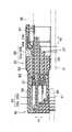
図9において、アングルタイプのコネクタ42にストレートタイプのコネクタ43が嵌合接続されている。アングルタイプのコネクタ42においては、特定コンタクトグループの信号コンタクト28aの各々は、第3の方向A3における一方の端部から第1の方向A1で基板接続部32と平行にのびて基板31に接続される特定接続部44を有している。特定接続部44の先端は基板31の表面に接続される表面実装端子45とされている。
【0040】
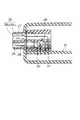
ストレートタイプのコネクタ43は、インシュレータ46と、このインシュレータ46に保持された導電性の筒状の嵌合部47と、この嵌合部47の内側に配置され且つインシュレータ46に保持された複数の導電性コンタクト(参照符号48で代表する)とを含んでいる。導電性コンタクト48は、アングルタイプのコネクタ42の導電性コンタクト28に一対一で対応して接触するものである。従って、これらの導電性コンタクト48も、特定コンタクトグループに対応するものでは、信号の通路となる信号コンタクト48aと、アースされるグランドコンタクト48bとに分かれている。信号コンタクト48aは第1の列に配列され、グランドコンタクト48bは第1の列に第1の方向A1で隣接した第2の列に配列されている。信号コンタクト48aはシールドケーブル49の信号線49aに接続されるものである。グランドコンタクト48bはシールドケーブル49のシールド線49bに接続されるものである。
【0041】
図10−図12を参照して、シールドケーブル49の接続について説明する。
【0042】
シールドケーブル49の接続のため、シールドケーブル49のシールド線49bが露出した部分を囲んで位置決めする囲い部51をグランドコンタクト48bに設ける。シールド線49bはそのリード部をグランドコンタクト48bに直接に半田付けなどにより接続する。囲い部51は、図11(a)又は(b)に示す形状に作られてもよいし、また図12に示す形状に作られてもよい。
【0043】
図13を参照して、シールドケーブル49の接続の変形例について説明する。
【0044】
図13において、アングルタイプのコネクタ42にアングルタイプのコネクタ52が嵌合接続されている。なお、両コネクタ42,52は基板31,51に夫々に搭載されている。
【0045】
コネクタ52は、インシュレータ53と、このインシュレータ53に保持された導電性の筒状の嵌合部54と、この嵌合部54の内側に配置され且つインシュレータ53に保持された複数の導電性コンタクト(参照符号55で代表する)とを含んでいる。導電性コンタクト55は、コネクタ42の導電性コンタクト28に一対一で対応して接触するものである。従って、これらの導電性コンタクト55も、特定コンタクトグループに対応するものでは、信号の通路となる信号コンタクト55aと、アースされるグランドコンタクト55bとに分かれている。信号コンタクト55aは第1の列に配列され、グランドコンタクト55bは第1の列に第1の方向A1で隣接した第2の列に配列されている。信号コンタクト55aはシールドケーブル49の信号線49aに接続されるものである。グランドコンタクト55bはシールドケーブル49のシールド線49bに接続されるものである。なお、特定コンタクトグループを除く他のコンタクトグループにおいては、導電性コンタクト55の各々は、第3の方向A3における端部から第1の方向A1で基板51に向かってのびて基板51に接続される基板接続部56を有している。
【0046】
特定コンタクトグループにおいては、導電性コンタクト55の各々はストレートタイプのものであり、コネクタ42の導電性コンタクト28と接触するための第1の接触部を第3の方向A3の一端に有し、シールドケーブル49と接続するための第2の接触部を第3の方向A3の他端に有している。
【0047】
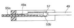
コネクタ52の導電性コンタクト55の第2の接触部にシールドケーブル49を接続するため、導電性コンタクト55とは別体に作られたロケータ57を用いる。ロケータ57はシールドケーブル49を位置決めしかつインシュレータ53に係合し、シールドケーブル49の信号線49aを信号コンタクト55aに、シールド線49bをグランドコンタクト55bに、夫々接続させるものである。
【0048】
ロケータ57は、インシュレータ58と、これに保持されかつシールド線49bに接続された導体部59を有し、その導体部59をグランドコンタクト55bに第3の方向A3のスライドを伴って接触させることで、シールド線49bをグランドコンタクト55bに接続させる。この状態で、ロケータ57はインシュレータ53に係合し、信号線49aが信号コンタクト55aに接続される。
【0049】
図14及び図15を参照して、シールドケーブル49の接続の他の変形例を説明する。
【0050】
グランドコンタクト55bには、交互に、シールド線49bの接触を助成する処理部61と、導体部59に圧接するばね部62とを有している。一方、シールド線49bにはリード部63を加工する。
【0051】
図14のようにシールドケーブル49を接続したロケータ57を、図15のようにコネクタ51に組付けると、導体部59がばね部62に圧接しかつリード部63が処理部61に接触する。こうしてシールド線49bがグランドコンタクト55bに接続される。また、信号線49aは信号コンタクト55aに半田付けなどにより接続される。
【0052】
なお、図14に示すように、シールドケーブル49を囲んで位置決めする囲い部57aをロケータ57に設けてもよい。また、シールドケーブル49のシールド線49bが露出した部分を囲んで位置決めする囲い部をロケータ57に設けてもよい。
【0053】
図16に示すように、シールド線49bのリード部63をロケータ57の導体部59に圧接や圧着や半田付けなどにより接続してもよい。
【0054】
図17に示すように、ロケータ57の導体部59の一部57aをグランドコンタクト55bの孔に差し込むことにより、導体部59とグランドコンタクト55bとの電気的導通を得てもよい。
【0055】
ロケータ57の導体部59はグランドコンタクト55bの孔に対し、図18に示すように第3の方向A3で差し込まれてもよいし、図19に示すように第1の方向A1で差し込まれてもよい。
【0056】
図20に示すように、グランドコンタクト55bに設けたばね部62によってシールド線49bとグランドコンタクト55bとの電気的導通を得るようにしてもよい。
【0057】
なお、図18−図20の構造では、特定コンタクトグループがコネクタ52の下部に位置している。
【0058】
図14ではグランドコンタクト55bにばね部62を設けているが、その代わりに、図21に示すようにロケータ57の導体部59にばね部64を設けてもよい。
【0059】
また図22に示すように、シールド線49bのリード部63をグランドコンタクト55bに直接に圧接や圧着や半田付けなどにより接続してもよい。
【0060】
図23を参照して、本発明の適用例を説明する。
【0061】
ディスプレイ機器71に接続したコネクタ72は、上述したコネクタと同様に、嵌合部の内側にコンタクトを各用途毎に集めてなるコンタクトグループを複数形成したものとする。一方、DVC73,74に備えたコネクタ75,76や、ゲーム機器77に備えたコネクタ78や、携帯電話機79に備えたコネクタ81は、コネクタ72の各コンタクトグループに接続可能なものとする。これによると、ディスプレイ機器71に接続した一つのコネクタ72に、DVC73,74やゲーム機器77や携帯電話機79を選択的に接続することができる。したがって、ディスプレイ機器71のコネクタ設備をシンプルに構成できる。ここで、コネクタ75はストレートタイプのコネクタであり、コネクタ76はアングルタイプのコネクタである。
【0062】
なお、ここではディスプレイ機器とDVCやゲーム機器や携帯電話機との接続を例にとって説明したが、その他の様々な接続に本発明が適用可能なことは勿論である。
【0063】
【発明の効果】
以上説明したように、本発明によれば、高速信号の取り扱いに有利な形態でコンタクトを用途毎に集めてグループ化したコネクタ、及びそのコネクタを備えた情報処理機器を提供することができる。
【図面の簡単な説明】
【図1】本発明の第1の実施の形態に係るコネクタを示し、(a)は正面図、(b)は平面図、(c)は右側面図である。
【図2】図1のコネクタの要部の断面図である。
【図3】本発明の第2の実施の形態に係るコネクタを示し、(a)は正面図、(b)は平面図、(c)は右側面図である。
【図4】図3のコネクタの取付状態を示す断面図である。
【図5】図1のコネクタを用いて中継接続により信号を伝送する場合を説明するための斜視図である。
【図6】図3のコネクタを用いて基板を経由して信号を伝送する場合を説明するための斜視図である。
【図7】図1のコネクタと図3のコネクタとを合体させたコネクタを用いて信号を伝送する場合の変形例を説明するための斜視図である。
【図8】図1のコネクタの変形例を用いて中継接続により信号を伝送する場合を説明するための斜視図である。
【図9】図1のコネクタの変形例と図3のコネクタの変形例とを互いに接続させた状態の断面図である。
【図10】コネクタの信号コンタクトとグランドコンタクトとにシールドケーブルを接続する構造を示す部分図である。
【図11】 図3のコネクタの二つの変形例を互いに接続させた状態の断面図である。
【図12】シールドコンタクトに設けた囲い部をシールドケーブルと共に示す変形例の説明図である。
【図13】図3のコネクタの二つの変形例を互いに接0続させた状態の断面図である。
【図14】コネクタに対しロケータを用いてシールドケーブルを接続する構造の接続前の状態を示す断面図である。
【図15】コネクタに対しロケータを用いてシールドケーブルを接続する構造の接続後の状態を示す断面図である。
【図16】ロケータとシールドケーブルとの接続の変形例を示す断面図である。
【図17】ロケータとシールドコンタクトとの接続の変形例を示す断面図である。
【図18】本発明の他の実施の形態に係るコネクタの断面図である。
【図19】本発明のさらに他の実施の形態に係るコネクタの断面図である。
【図20】本発明のさらに他の実施の形態に係るコネクタの断面図である。
【図21】ロケータの変形例を示す断面図である。
【図22】シールドケーブルのシールド線をグランドコンタクトに接続する変形例を示すコネクタの断面図である。
【図23】 本発明の適用例を示す説明図である。
【図24】従来のコネクタを備えたパーソナルコンピュータの使用形態を説明するための斜視図である。
【符号の説明】
21,26,46,53 インシュレータ
22,27,47,54 嵌合部
23,28,48,55 導電性コンタクト
23a,28a,48a,55a 信号コンタクト
23b,28b,48b,55b グランドコンタクト
24,29 コンタクトグループ
25 中継用コネクタ
31 基板
32,56 基板接続部
42 アングルタイプのコネクタ
43 ストレートタイプのコネクタ
44 特定接続部
45 表面実装端子
49 シールドケーブル
49a 信号線
49bシールド線
51 囲い部
52 アングルタイプのコネクタ
57 ロケータ
58 インシュレータ
59 導体部
61 処理部
62 ばね部
63 リード部
64 ばね部
71 ディスプレイ機器
72 コネクタ
73,74 DVC
75,76 コネクタ
77 ゲーム機器
78 コネクタ
79 携帯電話機
81 コネクタ[0001]
BACKGROUND OF THE INVENTION
The present invention relates to a connector in which a plurality of conductive contacts are arranged in a fitting portion held by an insulator.
[0002]
[Prior art]
For example, information processing devices such as personal computers handle various types of signals. In order to input and output these signals, as shown in FIG. 24, the
[0003]
The
[0004]
Thus, the
[0005]
[Problems to be solved by the invention]
However, since the
[0006]
In addition, in the case of personal computers made by different manufacturers, even if the same connector is used, the pin assignments may differ for each manufacturer, causing inconvenience in connecting peripheral devices and docking stations. It was.
[0007]
In addition, when it is desired to connect only to a certain circuit block, it is necessary to separately mount a dedicated connector on the personal computer, which has a drawback of high connector costs and mounting costs.
[0008]
SUMMARY OF THE INVENTION Therefore, an object of the present invention is to provide a connector that eliminates the above-mentioned drawbacks by collecting and grouping contacts for each application in a form advantageous for handling high-speed signals.
[0009]
The other subject of this invention is providing the information processing apparatus provided with the connector mentioned above.
[0010]
[Means for Solving the Problems]
According to one aspect of the present invention, the insulator and a plurality of conductive contacts held by the insulator, and theconductive contact and a locator made separately, the conductive contacts for each application A plurality of contact groups that are collected and adjacent to each other in a first direction, wherein the conductive contacts are arranged in a second direction orthogonal to the first direction, and the contacts The outermost contact group in the first direction of the group is assigned to the high-speed signal as a specific contact group, and the conductive contact has a signal contact serving as a signal path and a ground contact grounded. The specific contact group includes a first row of the signal contacts and the group. And a second row adjacent in the first direction in the first row consists of command contact, the locatoris what is or away with the slide to the ground contact, the shield of the shielded cable An enclosure portion that surrounds and positions the exposed wire; a conductor portionthat extends from the enclosure portion; anda spring portion thatcontacts the ground contact ,wherein the ground contact is a shield wire of a shielded cable. A connector is providedwhich has a processing section for assisting contact of the shield cable and connects the lead portion of the shielded wire of the shielded cableto the processing section of the ground contact when the locator contactsthe ground contact.
According to another aspect of the present invention, an insulator, a plurality of conductive contacts held by the insulator, and aconductive locator that is formed separately from theconductive contacts and positions a shield cable, The conductive contacts are collected for each application and are grouped into a plurality of contact groups adjacent to each other in a first direction, and the conductive contacts in the contact group are in a second direction orthogonal to the first direction. The outermost contact group in the first direction among the contact groups is assigned to a high-speed signal as a specific contact group, and the conductive contact is a signal contact serving as a signal path; And the specific contact group includes the ground contact. Wherein a first row consisting of contacts, and a second row adjacent in the first direction in the first row becomes than the ground contact, the locatorcontact away with the slide to the ground contact is what is said and enclosure which shielded wires of the shielded cable to position surrounds the portion exposed,the conductor portion connectedto the leadportion of the shield wire of the shield cable extending from the surroundingportion, the groundhave aspring portion for contacting thecontact, theconnector the locator and whereinthe conductor portion canbe connected to the ground contact when in contact with the ground contacts can be obtained.
[0012]
Each of the conductive contacts extends in a third direction orthogonal to the first and second directions, and one of the contact groups at both ends in the first direction is the specific contact group. May be.
[0013]
Each of the conductive contacts of the other contact groups excluding the specific contact group is connected to the substrate extending from the end in the third direction in a direction away from the specific contact group in the first direction. The contact group that is farthest from the substrate may be the specific contact group.
[0014]
Each of the conductive contacts of the specific contact group has a first contact portion for connecting to a mating connector at one end in the third direction, and a relay connector at the other end in the third direction. You may have the 2nd contact part for connecting.
[0015]
Each of the conductive contacts of the specific contact group may include a specific connection portion that extends in parallel with the substrate connection portion in the first direction from the end portion in the third direction and is connected to the substrate. Good.
[0016]
The specific connection portion may have a surface mount terminal connected to the surface of the substrate.
[0023]
The spring portion may beprovided in the ground contact instead of the locator .
[0025]
DETAILED DESCRIPTION OF THE INVENTION
With reference to FIG.1 and FIG.2, the connector which concerns on the 1st Embodiment of this invention is demonstrated.
[0026]
The illustrated connector is a receptacle, and includes an
[0027]
Of the
[0028]
Each of the
[0029]
A cable is connected to the
[0030]
With reference to FIGS. 3 and 4, a connector according to a second embodiment of the present invention will be described.
[0031]
The connector shown in the figure is also a receptacle, and includes an
[0032]
Of the
[0033]
Further, each
[0034]
Various connection examples will be described with reference to FIGS.
[0035]
A connector similar to the connector shown in FIGS. When signals are transmitted using the
[0036]
Furthermore, as shown in FIG. 7, the
[0037]
Further, as shown in FIG. 8, the
[0038]
A modification of the connector shown in FIGS. 3 and 4 will be described with reference to FIG. Similar parts are denoted by the same reference numerals and description thereof is omitted.
[0039]
In FIG. 9, a
[0040]
The
[0041]
The connection of the shielded
[0042]
In order to connect the shielded
[0043]
A modified example of the connection of the shielded
[0044]
In FIG. 13, an
[0045]
The
[0046]
In the specific contact group, each of the
[0047]
In order to connect the
[0048]
The
[0049]
With reference to FIG.14 and FIG.15, the other modification of the connection of the
[0050]
The
[0051]
When the
[0052]
As shown in FIG. 14, the
[0053]
As shown in FIG. 16, the
[0054]
As shown in FIG. 17, the
[0055]
The
[0056]
As shown in FIG. 20, electrical conduction between the
[0057]
18 to 20, the specific contact group is located below the
[0058]
In FIG. 14, the
[0059]
Further, as shown in FIG. 22, the
[0060]
An application example of the present invention will be described with reference to FIG.
[0061]
Assume that the
[0062]
Here, the connection between the display device and the DVC, the game device, and the mobile phone has been described as an example, but the present invention is naturally applicable to various other connections.
[0063]
【The invention's effect】
As described above, according to the present invention, it is possible to provide a connector in which contacts are collected for each application in a form advantageous for handling high-speed signals, and an information processing device including the connector.
[Brief description of the drawings]
1A and 1B show a connector according to a first embodiment of the present invention, in which FIG. 1A is a front view, FIG. 1B is a plan view, and FIG. 1C is a right side view;
FIG. 2 is a cross-sectional view of a main part of the connector of FIG.
3A and 3B show a connector according to a second embodiment of the present invention, in which FIG. 3A is a front view, FIG. 3B is a plan view, and FIG. 3C is a right side view.
4 is a cross-sectional view showing a mounting state of the connector of FIG. 3. FIG.
FIG. 5 is a perspective view for explaining a case where a signal is transmitted by relay connection using the connector of FIG. 1;
6 is a perspective view for explaining a case where a signal is transmitted through a board using the connector of FIG. 3; FIG.
7 is a perspective view for explaining a modification in the case of transmitting a signal using a connector in which the connector of FIG. 1 and the connector of FIG. 3 are combined.
FIG. 8 is a perspective view for explaining a case where a signal is transmitted by relay connection using a modification of the connector of FIG. 1;
9 is a cross-sectional view of a state in which a modification of the connector of FIG. 1 and a modification of the connector of FIG.
FIG. 10 is a partial view showing a structure for connecting a shielded cable to a signal contact and a ground contact of a connector.
11 is a cross-sectional view of a state in which two modifications of the connector of FIG. 3 areconnected to each other.
FIG. 12 is an explanatory view of a modified example in which an enclosure provided on a shield contact is shown together with a shield cable.
13 is a cross-sectional view of a state in which two modifications of the connector of FIG. 3 are connected to each other. FIG.
FIG. 14 is a cross-sectional view showing a state before connection of a structure in which a shield cable is connected to a connector using a locator.
FIG. 15 is a cross-sectional view showing a state after connection of a structure in which a shield cable is connected to a connector using a locator.
FIG. 16 is a cross-sectional view showing a modified example of connection between a locator and a shield cable.
FIG. 17 is a cross-sectional view showing a modified example of connection between a locator and a shield contact.
FIG. 18 is a cross-sectional view of a connector according to another embodiment of the present invention.
FIG. 19 is a cross-sectional view of a connector according to still another embodiment of the present invention.
FIG. 20 is a cross-sectional view of a connector according to still another embodiment of the present invention.
FIG. 21 is a cross-sectional view showing a modification of the locator.
FIG. 22 is a cross-sectional view of a connector showing a modified example in which the shield wire of the shield cable is connected to the ground contact.
FIG. 23 is an explanatory diagram showingan application example of the presentinvention .
FIG. 24 is a perspective view for explaining a usage pattern of a personal computer including a conventional connector.
[Explanation of symbols]
21, 26, 46, 53
75,76
Claims (8)
Translated fromJapanesePriority Applications (7)
| Application Number | Priority Date | Filing Date | Title |
|---|---|---|---|
| JP2000190976AJP3755865B2 (en) | 2000-06-26 | 2000-06-26 | connector |
| US09/880,611US6524119B2 (en) | 2000-06-26 | 2001-06-13 | Connector adapted to handling of different kinds of signals including high-speed signals |
| CNB011188154ACN1169265C (en) | 2000-06-26 | 2001-06-15 | Connectors suitable for handling different types of signals including high-speed signals |
| EP01115103AEP1168525B1 (en) | 2000-06-26 | 2001-06-21 | Connector adapted to handling of different kinds of signals including high-speed signals |
| DE60105701TDE60105701T2 (en) | 2000-06-26 | 2001-06-21 | For the processing of different types of signals including high speed signals usable connector |
| TW090115243ATW517414B (en) | 2000-06-26 | 2001-06-22 | Connector adapted to handling of different kinds of signals including high-speed signals |
| KR10-2001-0036690AKR100385489B1 (en) | 2000-06-26 | 2001-06-26 | Connector adapted to handling of different kinds of signals including high-speed signals |
Applications Claiming Priority (1)
| Application Number | Priority Date | Filing Date | Title |
|---|---|---|---|
| JP2000190976AJP3755865B2 (en) | 2000-06-26 | 2000-06-26 | connector |
Publications (2)
| Publication Number | Publication Date |
|---|---|
| JP2002008795A JP2002008795A (en) | 2002-01-11 |
| JP3755865B2true JP3755865B2 (en) | 2006-03-15 |
Family
ID=18690354
Family Applications (1)
| Application Number | Title | Priority Date | Filing Date |
|---|---|---|---|
| JP2000190976AExpired - Fee RelatedJP3755865B2 (en) | 2000-06-26 | 2000-06-26 | connector |
Country Status (7)
| Country | Link |
|---|---|
| US (1) | US6524119B2 (en) |
| EP (1) | EP1168525B1 (en) |
| JP (1) | JP3755865B2 (en) |
| KR (1) | KR100385489B1 (en) |
| CN (1) | CN1169265C (en) |
| DE (1) | DE60105701T2 (en) |
| TW (1) | TW517414B (en) |
Families Citing this family (41)
| Publication number | Priority date | Publication date | Assignee | Title |
|---|---|---|---|---|
| JP2001313130A (en)* | 2000-04-28 | 2001-11-09 | Japan Aviation Electronics Industry Ltd | Connector that groups contacts |
| JP4348879B2 (en)* | 2001-07-17 | 2009-10-21 | 住友電装株式会社 | Connector device for equipment |
| JP2003303648A (en)* | 2002-04-09 | 2003-10-24 | Mitsubishi Electric Corp | connector |
| US7627343B2 (en)* | 2003-04-25 | 2009-12-01 | Apple Inc. | Media player system |
| US6776660B1 (en) | 2003-04-30 | 2004-08-17 | Japan Aviation Electronics Industry, Limited | Connector |
| US7673083B2 (en)* | 2004-04-27 | 2010-03-02 | Apple Inc. | Method and system for controlling video selection and playback in a portable media player |
| US7797471B2 (en) | 2004-04-27 | 2010-09-14 | Apple Inc. | Method and system for transferring album artwork between a media player and an accessory |
| US7441058B1 (en)* | 2006-09-11 | 2008-10-21 | Apple Inc. | Method and system for controlling an accessory having a tuner |
| US7529872B1 (en)* | 2004-04-27 | 2009-05-05 | Apple Inc. | Communication between an accessory and a media player using a protocol with multiple lingoes |
| US7529871B1 (en) | 2004-04-27 | 2009-05-05 | Apple Inc. | Communication between an accessory and a media player with multiple protocol versions |
| US7826318B2 (en)* | 2004-04-27 | 2010-11-02 | Apple Inc. | Method and system for allowing a media player to transfer digital audio to an accessory |
| US7529870B1 (en)* | 2004-04-27 | 2009-05-05 | Apple Inc. | Communication between an accessory and a media player with multiple lingoes |
| US7634605B2 (en) | 2004-04-27 | 2009-12-15 | Apple Inc. | Method and system for transferring stored data between a media player and an accessory |
| US7293122B1 (en) | 2004-04-27 | 2007-11-06 | Apple Inc. | Connector interface system facilitating communication between a media player and accessories |
| US7441062B2 (en) | 2004-04-27 | 2008-10-21 | Apple Inc. | Connector interface system for enabling data communication with a multi-communication device |
| US7895378B2 (en) | 2004-04-27 | 2011-02-22 | Apple Inc. | Method and system for allowing a media player to transfer digital audio to an accessory |
| US7526588B1 (en)* | 2004-04-27 | 2009-04-28 | Apple Inc. | Communication between an accessory and a media player using a protocol with multiple lingoes |
| US8117651B2 (en) | 2004-04-27 | 2012-02-14 | Apple Inc. | Method and system for authenticating an accessory |
| US7823214B2 (en)* | 2005-01-07 | 2010-10-26 | Apple Inc. | Accessory authentication for electronic devices |
| US7525216B2 (en)* | 2005-01-07 | 2009-04-28 | Apple Inc. | Portable power source to provide power to an electronic device via an interface |
| CN2802767Y (en)* | 2005-06-29 | 2006-08-02 | 华为技术有限公司 | Plug of connector |
| EP1961083B1 (en)* | 2005-11-23 | 2016-01-27 | Draeger Medical Systems, Inc. | A connector system |
| US7632114B2 (en)* | 2006-03-30 | 2009-12-15 | Apple Inc. | Interface connecter between media player and other electronic devices |
| US8006019B2 (en) | 2006-05-22 | 2011-08-23 | Apple, Inc. | Method and system for transferring stored data between a media player and an accessory |
| US7415563B1 (en) | 2006-06-27 | 2008-08-19 | Apple Inc. | Method and system for allowing a media player to determine if it supports the capabilities of an accessory |
| US7558894B1 (en)* | 2006-09-11 | 2009-07-07 | Apple Inc. | Method and system for controlling power provided to an accessory |
| US7540788B2 (en)* | 2007-01-05 | 2009-06-02 | Apple Inc. | Backward compatible connector system |
| US8095713B2 (en)* | 2007-09-04 | 2012-01-10 | Apple Inc. | Smart cables |
| US8208853B2 (en)* | 2008-09-08 | 2012-06-26 | Apple Inc. | Accessory device authentication |
| US8238811B2 (en)* | 2008-09-08 | 2012-08-07 | Apple Inc. | Cross-transport authentication |
| US9496620B2 (en) | 2013-02-04 | 2016-11-15 | Ubiquiti Networks, Inc. | Radio system for long-range high-speed wireless communication |
| US8836601B2 (en) | 2013-02-04 | 2014-09-16 | Ubiquiti Networks, Inc. | Dual receiver/transmitter radio devices with choke |
| US7934952B2 (en)* | 2009-07-29 | 2011-05-03 | Ubiquiti Networks | Coaxial cable connector system and method |
| US9543635B2 (en) | 2013-02-04 | 2017-01-10 | Ubiquiti Networks, Inc. | Operation of radio devices for long-range high-speed wireless communication |
| US9397820B2 (en) | 2013-02-04 | 2016-07-19 | Ubiquiti Networks, Inc. | Agile duplexing wireless radio devices |
| US9293817B2 (en) | 2013-02-08 | 2016-03-22 | Ubiquiti Networks, Inc. | Stacked array antennas for high-speed wireless communication |
| PL3648359T3 (en) | 2013-10-11 | 2025-03-31 | Ubiquiti Inc. | Wireless radio system optimization by persistent spectrum analysis |
| LT3114884T (en) | 2014-03-07 | 2020-02-10 | Ubiquiti Inc. | IDENTIFICATION AND AUTHENTICATION OF THE CIRCULAR DEVICE |
| WO2015134755A2 (en) | 2014-03-07 | 2015-09-11 | Ubiquiti Networks, Inc. | Devices and methods for networked living and work spaces |
| EP3120642B1 (en) | 2014-03-17 | 2023-06-07 | Ubiquiti Inc. | Array antennas having a plurality of directional beams |
| WO2015153717A1 (en) | 2014-04-01 | 2015-10-08 | Ubiquiti Networks, Inc. | Antenna assembly |
Family Cites Families (14)
| Publication number | Priority date | Publication date | Assignee | Title |
|---|---|---|---|---|
| US3591834A (en)* | 1969-12-22 | 1971-07-06 | Ibm | Circuit board connecting means |
| US4484792A (en) | 1981-12-30 | 1984-11-27 | Chabin Corporation | Modular electrical connector system |
| US4762500A (en)* | 1986-12-04 | 1988-08-09 | Amp Incorporated | Impedance matched electrical connector |
| US4917616A (en)* | 1988-07-15 | 1990-04-17 | Amp Incorporated | Backplane signal connector with controlled impedance |
| US5116239A (en)* | 1990-06-14 | 1992-05-26 | Amp Incorporated | Multiconductor flat cable connector, apparatus and method |
| JPH0741109Y2 (en)* | 1990-09-17 | 1995-09-20 | ヒロセ電機株式会社 | Electrical connector structure |
| US5125854A (en) | 1991-07-16 | 1992-06-30 | Molex Incorporated | Modular electrical connector |
| US5709557A (en)* | 1994-12-12 | 1998-01-20 | The Whitaker Corporation | Electrical connector for dual printed circuit boards |
| JPH08305464A (en) | 1995-04-28 | 1996-11-22 | Toshiba Corp | External expansion device for portable electronic devices |
| US6183301B1 (en)* | 1997-01-16 | 2001-02-06 | Berg Technology, Inc. | Surface mount connector with integrated PCB assembly |
| EP0908977A3 (en) | 1997-10-09 | 2000-06-21 | Molex Incorporated | Card connector with improved grounding terminal |
| US6261107B1 (en)* | 1998-01-16 | 2001-07-17 | Molex Incorporated | Surface mount connector having improved terminal structure |
| US6027345A (en)* | 1998-03-06 | 2000-02-22 | Hon Hai Precision Ind. Co., Ltd. | Matrix-type electrical connector |
| MY123239A (en)* | 1998-12-18 | 2006-05-31 | Molex Inc | Card-receiving connector with grounding terminal |
- 2000
- 2000-06-26JPJP2000190976Apatent/JP3755865B2/ennot_activeExpired - Fee Related
- 2001
- 2001-06-13USUS09/880,611patent/US6524119B2/ennot_activeExpired - Lifetime
- 2001-06-15CNCNB011188154Apatent/CN1169265C/ennot_activeExpired - Fee Related
- 2001-06-21DEDE60105701Tpatent/DE60105701T2/ennot_activeExpired - Lifetime
- 2001-06-21EPEP01115103Apatent/EP1168525B1/ennot_activeExpired - Lifetime
- 2001-06-22TWTW090115243Apatent/TW517414B/ennot_activeIP Right Cessation
- 2001-06-26KRKR10-2001-0036690Apatent/KR100385489B1/ennot_activeExpired - Fee Related
Also Published As
| Publication number | Publication date |
|---|---|
| CN1169265C (en) | 2004-09-29 |
| US20010055901A1 (en) | 2001-12-27 |
| DE60105701D1 (en) | 2004-10-28 |
| JP2002008795A (en) | 2002-01-11 |
| KR100385489B1 (en) | 2003-05-27 |
| CN1332497A (en) | 2002-01-23 |
| TW517414B (en) | 2003-01-11 |
| KR20020001611A (en) | 2002-01-09 |
| US6524119B2 (en) | 2003-02-25 |
| EP1168525A1 (en) | 2002-01-02 |
| DE60105701T2 (en) | 2006-02-16 |
| EP1168525B1 (en) | 2004-09-22 |
Similar Documents
| Publication | Publication Date | Title |
|---|---|---|
| JP3755865B2 (en) | connector | |
| US7131862B2 (en) | Electrical connector with horizontal ground plane | |
| US6902433B1 (en) | Connector receptacle | |
| JP2005527960A (en) | Paddle card termination for shielded cable | |
| JP4917784B2 (en) | connector | |
| CN101142720A (en) | electrical connector | |
| TW201025741A (en) | USB connector and contact array thereof | |
| WO2012134587A1 (en) | An innovative cable termination scheme | |
| JP4421427B2 (en) | Cable connector for balanced transmission | |
| US20060042816A1 (en) | Parallel-transmission flat cable equipped with connector unit | |
| CN113013680B (en) | Connector assembly | |
| CN112909659A (en) | Wire harness, connector, and connector | |
| US20050054226A1 (en) | Balanced transmission cable connector | |
| TWI286867B (en) | Electric connector | |
| JP4843263B2 (en) | Connector for flexible printed cable | |
| JP3802070B2 (en) | Non-resistive energy coupling for crosstalk reduction | |
| JP5338261B2 (en) | Electrical connector | |
| JP7701254B2 (en) | Connectors and harnesses | |
| CN111727666B (en) | Relay board, differential transmission wire with relay board, and cable with connector | |
| AU778232B2 (en) | An electrical circuit board and a multiconnector | |
| US6722899B2 (en) | Connective apparatus in which a number of contacts are grouped into a plurality of contact groups according to intended use | |
| EP1327928A1 (en) | Connector receptacle | |
| CN103311745A (en) | Electric connector and assembly thereof | |
| CN101867100A (en) | Universal serial bus connector and contact array thereof | |
| JP2025022714A (en) | Cable unit, inter-module connection structure and connector set |
Legal Events
| Date | Code | Title | Description |
|---|---|---|---|
| A131 | Notification of reasons for refusal | Free format text:JAPANESE INTERMEDIATE CODE: A131 Effective date:20041124 | |
| A521 | Written amendment | Free format text:JAPANESE INTERMEDIATE CODE: A523 Effective date:20050118 | |
| TRDD | Decision of grant or rejection written | ||
| A01 | Written decision to grant a patent or to grant a registration (utility model) | Free format text:JAPANESE INTERMEDIATE CODE: A01 Effective date:20051214 | |
| A61 | First payment of annual fees (during grant procedure) | Free format text:JAPANESE INTERMEDIATE CODE: A61 Effective date:20051219 | |
| R150 | Certificate of patent or registration of utility model | Free format text:JAPANESE INTERMEDIATE CODE: R150 Ref document number:3755865 Country of ref document:JP Free format text:JAPANESE INTERMEDIATE CODE: R150 | |
| FPAY | Renewal fee payment (event date is renewal date of database) | Free format text:PAYMENT UNTIL: 20100106 Year of fee payment:4 | |
| FPAY | Renewal fee payment (event date is renewal date of database) | Free format text:PAYMENT UNTIL: 20100106 Year of fee payment:4 | |
| FPAY | Renewal fee payment (event date is renewal date of database) | Free format text:PAYMENT UNTIL: 20110106 Year of fee payment:5 | |
| FPAY | Renewal fee payment (event date is renewal date of database) | Free format text:PAYMENT UNTIL: 20110106 Year of fee payment:5 | |
| FPAY | Renewal fee payment (event date is renewal date of database) | Free format text:PAYMENT UNTIL: 20110106 Year of fee payment:5 | |
| FPAY | Renewal fee payment (event date is renewal date of database) | Free format text:PAYMENT UNTIL: 20120106 Year of fee payment:6 | |
| FPAY | Renewal fee payment (event date is renewal date of database) | Free format text:PAYMENT UNTIL: 20120106 Year of fee payment:6 | |
| FPAY | Renewal fee payment (event date is renewal date of database) | Free format text:PAYMENT UNTIL: 20130106 Year of fee payment:7 | |
| R250 | Receipt of annual fees | Free format text:JAPANESE INTERMEDIATE CODE: R250 | |
| FPAY | Renewal fee payment (event date is renewal date of database) | Free format text:PAYMENT UNTIL: 20130106 Year of fee payment:7 | |
| FPAY | Renewal fee payment (event date is renewal date of database) | Free format text:PAYMENT UNTIL: 20130106 Year of fee payment:7 | |
| FPAY | Renewal fee payment (event date is renewal date of database) | Free format text:PAYMENT UNTIL: 20130106 Year of fee payment:7 | |
| FPAY | Renewal fee payment (event date is renewal date of database) | Free format text:PAYMENT UNTIL: 20130106 Year of fee payment:7 | |
| FPAY | Renewal fee payment (event date is renewal date of database) | Free format text:PAYMENT UNTIL: 20130106 Year of fee payment:7 | |
| FPAY | Renewal fee payment (event date is renewal date of database) | Free format text:PAYMENT UNTIL: 20130106 Year of fee payment:7 | |
| FPAY | Renewal fee payment (event date is renewal date of database) | Free format text:PAYMENT UNTIL: 20130106 Year of fee payment:7 | |
| FPAY | Renewal fee payment (event date is renewal date of database) | Free format text:PAYMENT UNTIL: 20130106 Year of fee payment:7 | |
| FPAY | Renewal fee payment (event date is renewal date of database) | Free format text:PAYMENT UNTIL: 20140106 Year of fee payment:8 | |
| R250 | Receipt of annual fees | Free format text:JAPANESE INTERMEDIATE CODE: R250 | |
| R250 | Receipt of annual fees | Free format text:JAPANESE INTERMEDIATE CODE: R250 | |
| R250 | Receipt of annual fees | Free format text:JAPANESE INTERMEDIATE CODE: R250 | |
| R250 | Receipt of annual fees | Free format text:JAPANESE INTERMEDIATE CODE: R250 | |
| R250 | Receipt of annual fees | Free format text:JAPANESE INTERMEDIATE CODE: R250 | |
| R250 | Receipt of annual fees | Free format text:JAPANESE INTERMEDIATE CODE: R250 | |
| R250 | Receipt of annual fees | Free format text:JAPANESE INTERMEDIATE CODE: R250 | |
| LAPS | Cancellation because of no payment of annual fees |