JP3753986B2 - 半導体装置の製造方法および基板処理装置 - Google Patents
半導体装置の製造方法および基板処理装置Download PDFInfo
- Publication number
- JP3753986B2 JP3753986B2JP2002021367AJP2002021367AJP3753986B2JP 3753986 B2JP3753986 B2JP 3753986B2JP 2002021367 AJP2002021367 AJP 2002021367AJP 2002021367 AJP2002021367 AJP 2002021367AJP 3753986 B2JP3753986 B2JP 3753986B2
- Authority
- JP
- Japan
- Prior art keywords
- boron
- film formation
- boron trichloride
- substrate
- pressure
- Prior art date
- Legal status (The legal status is an assumption and is not a legal conclusion. Google has not performed a legal analysis and makes no representation as to the accuracy of the status listed.)
- Expired - Lifetime
Links
Images


Landscapes
- Insulated Gate Type Field-Effect Transistor (AREA)
- Chemical Vapour Deposition (AREA)
Description
【発明の属する技術分野】
本発明は、半導体装置の製造方法および基板処理装置に関し、特に、減圧CVD法(化学気相堆積法)によって、ポリシリコンゲルマニウムまたはアモルファスシリコンゲルマニウムを成膜する半導体装置の製造方法および基板処理装置に関する。
【0002】
【従来の技術】
IC、LSI等の半導体デバイスを製造する工程においては、減圧CVD法(化学気相堆積法)によって、基板上に薄膜を成膜することが行われている。そのような成膜工程の中の一つとして、減圧CVD法によって、シリコンゲルマニウム膜を形成することが試みられている。
【0003】
シリコンゲルマニウムは、目的のデバイスによって、例えばヘテロ接合型バイポーラトランジスタ(HBT)ではベース領域にエピタキシャルシリコンゲルマニウムを成長させることやMOSトランジスタではゲート電極部分にポリシリコンゲルマニウム膜を形成することが試みられている。
【0004】
従来の減圧CVD装置によるポリシリコンゲルマニウム成膜において、ボロンをドーピングするのにジボラン(B2H6)が用いられていた。しかし、ジボランを用いた場合、バッチ処理である縦型減圧CVD装置においては、ウェハ面内・ウェハ面間でのシリコンゲルマニウム膜中でのボロン(B)濃度均一性を確保することが困難であった。そこで、ジボランの代替ドーピングガスとして三塩化ホウ素(BCl3)を用いることが行われた。三塩化ホウ素は、ジボランと比較して反応性が低いため、ガス流れ方向に対して、それほど消費が多くないので、ボロン濃度面間均一性を確保できる。またウェハ間隔が5.2mmピッチ程度と狭くても、三塩化ホウ素はウェハ中心部まで行き渡り、ボロン濃度面内均一性も良くなることがわかっている。
【0005】
【発明が解決しようとする課題】
シリコンゲルマニウム膜中でのボロン濃度の適正値は適用デバイス部分によって異なり、例えば、ゲート電極用では低抵抗化するために高濃度のボロンを導入する。ジボランによるシリコンゲルマニウム膜中のボロン濃度はジボラン分圧に比例して単調増加することがわかっている。しかしながら、塩素を含んでいる三塩化ホウ素の場合どのような挙動を示すのかわかっていない。そこで、三塩化ホウ素をドーピングガスとして用いた場合の、シリコンゲルマニウム膜中のボロンの挙動を明らかにすることは、適正な濃度のボロンドーピングを実行する上で、重要な課題となる。
【0006】
本発明の目的は、上記課題を解決し、減圧CVD法によって、適正なボロンドーピング濃度のボロンドープポリシリコンゲルマニウムまたはボロンドープアモルファスシリコンゲルマニウムを成膜することを可能とする半導体装置の製造方法および基板処理装置を提供することにある。
【0007】
【課題を解決するための手段】
前記課題を解決するために、本発明は、請求項1に記載のように、
反応ガスとしてモノシランとモノゲルマンとを使用し、反応炉内において、減圧CVD法により、基板上にMOSトランジスタのゲート電極としてボロンドープポリシリコンゲルマニウムまたはボロンドープアモルファスシリコンゲルマニウムを成膜する半導体装置の製造方法において、前記反応炉内の圧力を30Pa以上120Pa以下とし、ドーピングガスとして三塩化ホウ素を用い、成膜時における前記三塩化ホウ素の分圧を0.2Pa以上1Pa以下とし、成膜時における前記反応炉内の温度を450℃以上500℃以下とし、成膜時におけるモノシランに対する三塩化ホウ素の流量比を0.000017〜0.028とすることを特徴とする半導体装置の製造方法を構成する。
【0008】
また、本発明は、請求項2に記載のように、
基板上にMOSトランジスタのゲート電極としてボロンドープポリシリコンゲルマニウムまたはボロンドープアモルファスシリコンゲルマニウムを成膜する基板処理装置であって、前記基板を処理する反応管と、前記反応管内の前記基板を加熱するヒータと、前記反応管内に成膜用ガスであるモノシランを供給するノズルと、成膜用ガスであるモノゲルマンを供給するノズルと、ドーピングガスである三塩化ホウ素を供給するノズルと、前記反応管内を排気する排気管と、前記反応管内の圧力を30Pa以上120Pa以下とし、成膜時における前記反応炉内の温度を450℃以上500℃以下とし、成膜時におけるモノシランに対する三塩化ホウ素の流量比を0.000017〜0.028とし、成膜時の前記三塩化ホウ素の分圧を0.2Pa以上1Pa以下に制御する制御装置とを有することを特徴とする基板処理装置を構成する。
【0009】
【発明の実施の形態】
本発明者らは鋭意検討の結果、三塩化ホウ素をドーピングガスとして用いた場合においてシリコンゲルマニウム膜中に取り込まれるボロン濃度と三塩化ホウ素の分圧との関係を究明し、その結果に基づいて本発明をなすに到った。
【0010】
本発明に係る半導体装置の製造方法は、本発明に係る基板処理装置の一つである縦型減圧CVD装置において、反応ガスとしてモノシラン(SiH4)及びモノゲルマン(GeH4)、ドーピングガスとして三塩化ホウ素を使用し、ウェハ上にボロンドープポリシリコンゲルマニウムまたはボロンドープアモルファスシリコンゲルマニウムを成膜するものである。
【0011】
上記縦型減圧CVD装置の一例であるホットウォール縦型減圧CVD装置の反応炉構造概略図を図1に示す。図において、ホットウォール炉を構成し、基板を加熱する4ゾーン(U、CU、CLおよびL)に分かれたヒータ6の内側に、反応炉11の外筒である石英製のアウターチューブ1およびアウターチューブ1内部のインナーチューブ2が設置されており、この2種のチューブの間をメカニカルブースタポンプ7およびドライポンプ8を用いて真空引きしている。従って、インナーチューブ2内側に4本の途中供給ノズル12から反応ガスとしてモノゲルマン、SiH4+GeH4ノズル13から反応ガスとしてモノシランとモノゲルマンとの混合ガス、さらにBCl3ノズル14からドーピングガスとして三塩化ホウ素が導入され、反応ガスとドーピングガスとはインナーチューブ2内を上昇し、2種のチューブ1、2の間を下降して排気される。なお、各ガスの供給流量は各ガス供給系にそれぞれ設けられた図示しない流量制御装置により制御される。
【0012】
複数枚の基板であるウェハ4が垂直方向に積層されて装填された積載基板支持具である石英製のボート3(例えば8インチウェハ用、ウェハ間間隔5.2mmピッチ)はインナーチューブ2内に設置され、反応ガスにさらされた時に気相中およびウェハ4表面での反応により、ウェハ4上にボロンドープシリコンゲルマニウム薄膜が形成される。その際、反応炉11内の圧力を制御するために、N2バラスト用バルブ16を通して窒素(N2)を排気系に導入し、その窒素の流量を、コントローラ17が、圧力計15の出力信号に基づいて制御する。なお、三塩化ホウ素の分圧は、炉内圧力と、総流量、BCl3流量の比率を調整することにより制御する。しかし、炉内圧力(成長圧力)は、ウェハ面内の膜厚均一性に大きく影響を及ぼすので、本実施形態では、BCl3の流量を増減させることで、BCl3分圧を制御している。すなわち、本実施形態では、N2バラスト用バルブ16と圧力計15とコントローラ17とで構成される圧力制御装置と、三塩化ホウ素の流量を制御する流量制御装置(図示せず)とが請求項2に記載の、三塩化ホウ素の分圧を制御する制御装置を構成している。
【0013】
断熱板5はボート3と装置下部との間を断熱するためのものである。また9はボート回転軸であり、10はステンレス製蓋である。
【0014】
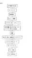
図2は、図1に示した基板処理装置を用いる成膜手順を示している。
【0015】
まず、複数枚のウェハ4をボート3に投入し、反応炉11内を成膜温度に安定化させた後、ウェハ4を装填したボート3を反応炉11内にロード(挿入)する。リアクター(反応炉11)内を排気し、ボート3やチューブ1、2に吸着した水分等を脱離させるためにN2パージを行う。
【0016】
その後、リアクター内リークチェックを行った後、各原料ガスの流量を設定し、反応炉11内に各ガスを流しながら成長圧力になるようN2バラストによって安定化させる。このとき、BCl3分圧は成長圧力と総流量、BCl3流量の比率の関係で決まる。しかし、前述のように、成長圧力はウェハ4面内の膜厚均一性に大きく影響を及ぼすので、本実施形態では、BCl3流量を増減させることでBCl3分圧を制御する。そして反応炉11内の成長圧力が安定した後、成膜を行う。
【0017】
成膜が終了したら、反応ガスの流入を停止し、配管内をN2でサイクルパージし、N2でリアクター(反応炉11)内を大気圧まで戻す。大気圧に戻ったらボート3をアンロードし、ウェハ4を自然冷却する。最後にウェハ4をボート3から取り出す。
【0018】
実施の形態例を以下に示す。
【0019】
図1に示す基板処理装置を用いて、8インチウェハに対してボロンドープシリコンゲルマニウムを成膜した。
【0020】
この場合の成膜条件は成膜温度450〜500℃、成長圧力30〜120Pa、GeH4/SiH4=0.038、BCl3/SiH4=0.000017〜0.028とした。なお、これらの比(GeH4/SiH4、BCl3/SiH4)は、それぞれ、SiH4に対するGeH4、BCl3の流量比を示している。
【0021】
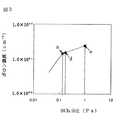
図3は、三塩化ホウ素の分圧を1.02×10⁻⁴〜2(Pa)の範囲で制御した内の0.05〜2Paまでの、三塩化ホウ素の分圧とボロン濃度との関係を示す。
【0022】
図3に示すように、三塩化ホウ素分圧を増加させることで単調増加し、三塩化ホウ素分圧“a”点でボロン濃度がおおよそ飽和することがわかった。この点は、シリコンゲルマニウム膜中に取り込まれるボロンの固溶限界領域付近にある。したがって、三塩化ホウ素の分圧を“a”点における分圧すなわち0.1Pa以上とすることにより、ボロンを最大限にドーピングすることができる。また、これから三塩化ホウ素の分圧を制御することにより任意のボロン濃度を得ることができることが判る。
【0023】
図4は、三塩化ホウ素によってドーピングされたボロンドープシリコンゲルマニウム膜の成膜直後のボロン濃度と抵抗率の関係を示した図である。図から、ボロン濃度の増加と共に抵抗率が低下していることがわかる。逆に、ボロン濃度の低下と共に、抵抗率は増加し、“b”点以下のボロン濃度になると抵抗率が高くなり過ぎ好ましくない。また、ボロン濃度が“c”点より高くなると、ボロン濃度が増加するにもかかわらず、抵抗率が高くなる傾向があり好ましくない。これらのことから、“b”点以上“c”点以下のボロン濃度範囲が、低抵抗化が必要であるゲート電極にとって適した範囲であるといえる。なお、図4の“b”点、“c”点におけるボロン濃度は図3の“d”点、“e”点におけるボロン濃度に対応している。従って、前述のようなゲート電極に適したボロン濃度範囲のシリコンゲルマニウム膜は、三塩化ホウ素の分圧を、図3の“d”点における分圧すなわち0.2Pa以上、“e”点における分圧すなわち1Pa以下とすることによって、成膜されることが判る。なお、三塩化ホウ素の分圧を1Paよりも大きくしても、図3に示したように、膜中のボロン濃度はわずかに増大するのみであり、しかも、図4に示したように、抵抗率は上昇するので、実用上有利ではない。
【0024】
このことから、三塩化ホウ素の分圧を、0.2Pa以上、1Pa以下とすることで、ゲート電極に適したボロン濃度のシリコンゲルマニウム膜を得ることができることが判る。このようなシリコンゲルマニウム膜の抵抗率は、成膜温度450〜500℃における成膜直後に実現するものであり、このことから、高温(500℃よりも高い温度)のアニール処理工程を用いなくても、低温(500℃以下)処理工程のみによって、低抵抗のシリコンゲルマニウム膜を成膜することができることが判る。
【0025】
なお、上記成膜条件を適宜決定すればアモルファス、ポリの何れの成膜も可能である。
【0026】
以上に説明したように、本発明の実施によって、縦型減圧CVD装置におけるボロンドープポリシリコンゲルマニウムまたはボロンドープアモルファスシリコンゲルマニウムを成膜する半導体の製造方法および基板処理装置において、三塩化ホウ素の分圧を制御することによりゲート電極に適したボロン濃度を得ることができ、高温のアニール処理工程を用いなくても低温で低抵抗化することができる半導体装置の製造方法および基板処理装置を提供することができる。
【0027】
【発明の効果】
本発明の実施によって、減圧CVD法によって、適正なボロン濃度のボロンドープポリシリコンゲルマニウムまたはボロンドープアモルファスシリコンゲルマニウムを成膜することを可能とする半導体装置の製造方法および基板処理装置を提供することができる。
【図面の簡単な説明】
【図1】本発明の実施の形態例である縦型減圧CVD装置の反応炉構造概略を示す図である。
【図2】減圧CVD法による成膜手順を説明する図である。
【図3】成膜工程中における三塩化ホウ素分圧とシリコンゲルマニウム膜中のボロン濃度との関係を示す図である。
【図4】シリコンゲルマニウム膜中のボロン濃度とシリコンゲルマニウム膜抵抗率との関係を示す図である。
【符号の説明】
1…アウターチューブ、2…インナーチューブ、3…ボート、4…ウェハ、5…断熱板、6…ヒータ、7…メカニカルブースタポンプ、8…ドライポンプ、9…ボート回転軸、10…ステンレス製蓋、11…反応炉、12…途中供給ノズル、13…SiH4+GeH4ノズル、14…BCl3ノズル、15…圧力計、16…N2バラスト用バルブ、17…コントローラ。
Claims (2)
- 反応ガスとしてモノシランとモノゲルマンとを使用し、反応炉内において、減圧CVD法により、基板上にMOSトランジスタのゲート電極としてボロンドープポリシリコンゲルマニウムまたはボロンドープアモルファスシリコンゲルマニウムを成膜する半導体装置の製造方法において、前記反応炉内の圧力を30Pa以上120Pa以下とし、ドーピングガスとして三塩化ホウ素を用い、成膜時における前記三塩化ホウ素の分圧を0.2Pa以上1Pa以下とし、成膜時における前記反応炉内の温度を450℃以上500℃以下とし、成膜時におけるモノシランに対する三塩化ホウ素の流量比を0.000017〜0.028とすることを特徴とする半導体装置の製造方法。
- 基板上にMOSトランジスタのゲート電極としてボロンドープポリシリコンゲルマニウムまたはボロンドープアモルファスシリコンゲルマニウムを成膜する基板処理装置であって、前記基板を処理する反応管と、前記反応管内の前記基板を加熱するヒータと、前記反応管内に成膜用ガスであるモノシランを供給するノズルと、成膜用ガスであるモノゲルマンを供給するノズルと、ドーピングガスである三塩化ホウ素を供給するノズルと、前記反応管内を排気する排気管と、前記反応管内の圧力を30Pa以上120Pa以下とし、成膜時における前記反応炉内の温度を450℃以上500℃以下とし、成膜時におけるモノシランに対する三塩化ホウ素の流量比を0.000017〜0.028とし、成膜時の前記三塩化ホウ素の分圧を0.2Pa以上1Pa以下に制御する制御装置とを有することを特徴とする基板処理装置。
Priority Applications (1)
| Application Number | Priority Date | Filing Date | Title |
|---|---|---|---|
| JP2002021367AJP3753986B2 (ja) | 2002-01-30 | 2002-01-30 | 半導体装置の製造方法および基板処理装置 |
Applications Claiming Priority (1)
| Application Number | Priority Date | Filing Date | Title |
|---|---|---|---|
| JP2002021367AJP3753986B2 (ja) | 2002-01-30 | 2002-01-30 | 半導体装置の製造方法および基板処理装置 |
Publications (2)
| Publication Number | Publication Date |
|---|---|
| JP2003224075A JP2003224075A (ja) | 2003-08-08 |
| JP3753986B2true JP3753986B2 (ja) | 2006-03-08 |
Family
ID=27744627
Family Applications (1)
| Application Number | Title | Priority Date | Filing Date |
|---|---|---|---|
| JP2002021367AExpired - LifetimeJP3753986B2 (ja) | 2002-01-30 | 2002-01-30 | 半導体装置の製造方法および基板処理装置 |
Country Status (1)
| Country | Link |
|---|---|
| JP (1) | JP3753986B2 (ja) |
Families Citing this family (1)
| Publication number | Priority date | Publication date | Assignee | Title |
|---|---|---|---|---|
| US7772097B2 (en) | 2007-11-05 | 2010-08-10 | Asm America, Inc. | Methods of selectively depositing silicon-containing films |
- 2002
- 2002-01-30JPJP2002021367Apatent/JP3753986B2/janot_activeExpired - Lifetime
Also Published As
| Publication number | Publication date |
|---|---|
| JP2003224075A (ja) | 2003-08-08 |
Similar Documents
| Publication | Publication Date | Title |
|---|---|---|
| US6686281B2 (en) | Method for fabricating a semiconductor device and a substrate processing apparatus | |
| JP3265042B2 (ja) | 成膜方法 | |
| JP3437832B2 (ja) | 成膜方法及び成膜装置 | |
| JP5383784B2 (ja) | 半導体装置の製造方法、基板処理方法及び基板処理装置 | |
| JP3356531B2 (ja) | ボロン含有ポリシリコン膜の形成方法 | |
| JP5697849B2 (ja) | 半導体装置の製造方法及び基板処理装置 | |
| JP5220049B2 (ja) | 炭化珪素半導体装置の製造方法 | |
| US5677235A (en) | Method for forming silicon film | |
| KR100860683B1 (ko) | 성막 방법 및 열처리 장치 | |
| JPH0786174A (ja) | 成膜装置 | |
| JPH10321361A (ja) | 高周波誘導加熱コイル、半導体製造装置、および高周波誘導加熱コイルの製造方法 | |
| US5783257A (en) | Method for forming doped polysilicon films | |
| JP3753986B2 (ja) | 半導体装置の製造方法および基板処理装置 | |
| JP3938877B2 (ja) | 半導体装置の製造方法 | |
| JP4792180B2 (ja) | 半導体デバイスの製造方法、基板処理方法および基板処理装置 | |
| JP3806410B2 (ja) | 半導体デバイスの製造方法及び半導体製造装置 | |
| JP2822756B2 (ja) | 気相成長装置およびその薄膜形成方法 | |
| JP4456341B2 (ja) | 半導体装置の製造方法および基板処理装置 | |
| JP3100702B2 (ja) | 減圧化学反応方法及びその装置 | |
| JP4892579B2 (ja) | 半導体装置の製造方法 | |
| EP4174209A1 (en) | Method of forming a doped polysilicon layer | |
| US20020016051A1 (en) | Method for manufacturing semiconductor device, substrate treatment method, and semiconductor manufacturing apparatus | |
| JPH07307292A (ja) | 成膜方法およびこれに用いる減圧cvd装置 | |
| JP2025158809A (ja) | 成膜方法 | |
| JP2013089833A (ja) | 半導体装置の製造方法 |
Legal Events
| Date | Code | Title | Description |
|---|---|---|---|
| A621 | Written request for application examination | Free format text:JAPANESE INTERMEDIATE CODE: A621 Effective date:20040929 | |
| A977 | Report on retrieval | Free format text:JAPANESE INTERMEDIATE CODE: A971007 Effective date:20050516 | |
| A131 | Notification of reasons for refusal | Free format text:JAPANESE INTERMEDIATE CODE: A131 Effective date:20050614 | |
| A521 | Request for written amendment filed | Free format text:JAPANESE INTERMEDIATE CODE: A523 Effective date:20050803 | |
| A02 | Decision of refusal | Free format text:JAPANESE INTERMEDIATE CODE: A02 Effective date:20050830 | |
| A521 | Request for written amendment filed | Free format text:JAPANESE INTERMEDIATE CODE: A523 Effective date:20051017 | |
| A911 | Transfer to examiner for re-examination before appeal (zenchi) | Free format text:JAPANESE INTERMEDIATE CODE: A911 Effective date:20051021 | |
| TRDD | Decision of grant or rejection written | ||
| A01 | Written decision to grant a patent or to grant a registration (utility model) | Free format text:JAPANESE INTERMEDIATE CODE: A01 Effective date:20051213 | |
| A61 | First payment of annual fees (during grant procedure) | Free format text:JAPANESE INTERMEDIATE CODE: A61 Effective date:20051214 | |
| R150 | Certificate of patent or registration of utility model | Free format text:JAPANESE INTERMEDIATE CODE: R150 Ref document number:3753986 Country of ref document:JP Free format text:JAPANESE INTERMEDIATE CODE: R150 | |
| FPAY | Renewal fee payment (event date is renewal date of database) | Free format text:PAYMENT UNTIL: 20091222 Year of fee payment:4 | |
| FPAY | Renewal fee payment (event date is renewal date of database) | Free format text:PAYMENT UNTIL: 20091222 Year of fee payment:4 | |
| FPAY | Renewal fee payment (event date is renewal date of database) | Free format text:PAYMENT UNTIL: 20101222 Year of fee payment:5 | |
| FPAY | Renewal fee payment (event date is renewal date of database) | Free format text:PAYMENT UNTIL: 20111222 Year of fee payment:6 | |
| FPAY | Renewal fee payment (event date is renewal date of database) | Free format text:PAYMENT UNTIL: 20111222 Year of fee payment:6 | |
| FPAY | Renewal fee payment (event date is renewal date of database) | Free format text:PAYMENT UNTIL: 20121222 Year of fee payment:7 | |
| FPAY | Renewal fee payment (event date is renewal date of database) | Free format text:PAYMENT UNTIL: 20121222 Year of fee payment:7 | |
| FPAY | Renewal fee payment (event date is renewal date of database) | Free format text:PAYMENT UNTIL: 20131222 Year of fee payment:8 | |
| S111 | Request for change of ownership or part of ownership | Free format text:JAPANESE INTERMEDIATE CODE: R313111 | |
| S531 | Written request for registration of change of domicile | Free format text:JAPANESE INTERMEDIATE CODE: R313531 | |
| R350 | Written notification of registration of transfer | Free format text:JAPANESE INTERMEDIATE CODE: R350 | |
| EXPY | Cancellation because of completion of term |