JP3749504B2 - PTC composition, thermistor element, and production method thereof - Google Patents
PTC composition, thermistor element, and production method thereofDownload PDFInfo
- Publication number
- JP3749504B2 JP3749504B2JP2002156142AJP2002156142AJP3749504B2JP 3749504 B2JP3749504 B2JP 3749504B2JP 2002156142 AJP2002156142 AJP 2002156142AJP 2002156142 AJP2002156142 AJP 2002156142AJP 3749504 B2JP3749504 B2JP 3749504B2
- Authority
- JP
- Japan
- Prior art keywords
- mixture
- ptc composition
- electron beam
- resistance
- temperature
- Prior art date
- Legal status (The legal status is an assumption and is not a legal conclusion. Google has not performed a legal analysis and makes no representation as to the accuracy of the status listed.)
- Expired - Fee Related
Links
- 239000000203mixtureSubstances0.000titleclaimsdescription99
- 238000004519manufacturing processMethods0.000titleclaimsdescription12
- 238000010894electron beam technologyMethods0.000claimsdescription48
- 229920000642polymerPolymers0.000claimsdescription39
- 239000011159matrix materialSubstances0.000claimsdescription35
- 150000002894organic compoundsChemical class0.000claimsdescription32
- 230000001133accelerationEffects0.000claimsdescription27
- PXHVJJICTQNCMI-UHFFFAOYSA-NNickelChemical compound[Ni]PXHVJJICTQNCMI-UHFFFAOYSA-N0.000claimsdescription20
- 238000002844meltingMethods0.000claimsdescription19
- 230000008018meltingEffects0.000claimsdescription19
- 238000004132cross linkingMethods0.000claimsdescription18
- 239000000463materialSubstances0.000claimsdescription16
- 239000004020conductorSubstances0.000claimsdescription13
- 239000004707linear low-density polyethyleneSubstances0.000claimsdescription13
- 239000000126substanceSubstances0.000claimsdescription12
- 230000001678irradiating effectEffects0.000claimsdescription9
- 229920000092linear low density polyethylenePolymers0.000claimsdescription9
- 229910000679solderInorganic materials0.000claimsdescription7
- VGGSQFUCUMXWEO-UHFFFAOYSA-NEtheneChemical compoundC=CVGGSQFUCUMXWEO-UHFFFAOYSA-N0.000claimsdescription5
- 239000005977EthyleneSubstances0.000claimsdescription5
- 229920001519homopolymerPolymers0.000claimsdescription5
- 239000012968metallocene catalystSubstances0.000claimsdescription5
- 239000007791liquid phaseSubstances0.000claims1
- 239000002245particleSubstances0.000description21
- 230000000052comparative effectEffects0.000description17
- -1polyethylene, ethylene-vinyl acetatePolymers0.000description17
- 230000008859changeEffects0.000description14
- 229920006038crystalline resinPolymers0.000description11
- 229910052751metalInorganic materials0.000description10
- 239000002184metalSubstances0.000description10
- 238000011156evaluationMethods0.000description9
- 238000000034methodMethods0.000description8
- 238000005476solderingMethods0.000description7
- VYPSYNLAJGMNEJ-UHFFFAOYSA-NSilicium dioxideChemical compoundO=[Si]=OVYPSYNLAJGMNEJ-UHFFFAOYSA-N0.000description6
- 239000011164primary particleSubstances0.000description5
- 230000035939shockEffects0.000description5
- UQSXHKLRYXJYBZ-UHFFFAOYSA-NIron oxideChemical compound[Fe]=OUQSXHKLRYXJYBZ-UHFFFAOYSA-N0.000description4
- 239000004743PolypropyleneSubstances0.000description4
- XLOMVQKBTHCTTD-UHFFFAOYSA-NZinc monoxideChemical compound[Zn]=OXLOMVQKBTHCTTD-UHFFFAOYSA-N0.000description4
- 239000000654additiveSubstances0.000description4
- 239000003963antioxidant agentSubstances0.000description4
- 239000006229carbon blackSubstances0.000description4
- 239000007772electrode materialSubstances0.000description4
- 239000011888foilSubstances0.000description4
- 238000004898kneadingMethods0.000description4
- CPLXHLVBOLITMK-UHFFFAOYSA-Nmagnesium oxideInorganic materials[Mg]=OCPLXHLVBOLITMK-UHFFFAOYSA-N0.000description4
- 229920000098polyolefinPolymers0.000description4
- 229920001155polypropylenePolymers0.000description4
- XLYOFNOQVPJJNP-UHFFFAOYSA-NwaterSubstancesOXLYOFNOQVPJJNP-UHFFFAOYSA-N0.000description4
- 239000002033PVDF binderSubstances0.000description3
- YXFVVABEGXRONW-UHFFFAOYSA-NTolueneChemical compoundCC1=CC=CC=C1YXFVVABEGXRONW-UHFFFAOYSA-N0.000description3
- PNEYBMLMFCGWSK-UHFFFAOYSA-Naluminium oxideInorganic materials[O-2].[O-2].[O-2].[Al+3].[Al+3]PNEYBMLMFCGWSK-UHFFFAOYSA-N0.000description3
- 230000003078antioxidant effectEffects0.000description3
- WPYMKLBDIGXBTP-UHFFFAOYSA-Nbenzoic acidChemical compoundOC(=O)C1=CC=CC=C1WPYMKLBDIGXBTP-UHFFFAOYSA-N0.000description3
- 230000005540biological transmissionEffects0.000description3
- 229920001577copolymerPolymers0.000description3
- 235000014113dietary fatty acidsNutrition0.000description3
- 239000000194fatty acidSubstances0.000description3
- 229930195729fatty acidNatural products0.000description3
- NPURPEXKKDAKIH-UHFFFAOYSA-Niodoimino(oxo)methaneChemical compoundIN=C=ONPURPEXKKDAKIH-UHFFFAOYSA-N0.000description3
- 239000000395magnesium oxideSubstances0.000description3
- 238000000465mouldingMethods0.000description3
- 229920002981polyvinylidene fluoridePolymers0.000description3
- 239000000843powderSubstances0.000description3
- 230000005855radiationEffects0.000description3
- 239000000377silicon dioxideSubstances0.000description3
- 239000000454talcSubstances0.000description3
- 229910052623talcInorganic materials0.000description3
- FMZUHGYZWYNSOA-VVBFYGJXSA-N(1r)-1-[(4r,4ar,8as)-2,6-diphenyl-4,4a,8,8a-tetrahydro-[1,3]dioxino[5,4-d][1,3]dioxin-4-yl]ethane-1,2-diolChemical compoundC([C@@H]1OC(O[C@@H]([C@@H]1O1)[C@H](O)CO)C=2C=CC=CC=2)OC1C1=CC=CC=C1FMZUHGYZWYNSOA-VVBFYGJXSA-N0.000description2
- NIXOWILDQLNWCW-UHFFFAOYSA-MAcrylateChemical compound[O-]C(=O)C=CNIXOWILDQLNWCW-UHFFFAOYSA-M0.000description2
- LTPBRCUWZOMYOC-UHFFFAOYSA-NBeryllium oxideChemical compoundO=[Be]LTPBRCUWZOMYOC-UHFFFAOYSA-N0.000description2
- VTYYLEPIZMXCLO-UHFFFAOYSA-LCalcium carbonateChemical compound[Ca+2].[O-]C([O-])=OVTYYLEPIZMXCLO-UHFFFAOYSA-L0.000description2
- OKTJSMMVPCPJKN-UHFFFAOYSA-NCarbonChemical compound[C]OKTJSMMVPCPJKN-UHFFFAOYSA-N0.000description2
- 229920000049Carbon (fiber)Polymers0.000description2
- RTZKZFJDLAIYFH-UHFFFAOYSA-NDiethyl etherChemical compoundCCOCCRTZKZFJDLAIYFH-UHFFFAOYSA-N0.000description2
- UFWIBTONFRDIAS-UHFFFAOYSA-NNaphthaleneChemical compoundC1=CC=CC2=CC=CC=C21UFWIBTONFRDIAS-UHFFFAOYSA-N0.000description2
- OAICVXFJPJFONN-UHFFFAOYSA-NPhosphorusChemical compound[P]OAICVXFJPJFONN-UHFFFAOYSA-N0.000description2
- 239000004721Polyphenylene oxideSubstances0.000description2
- 239000004734Polyphenylene sulfideSubstances0.000description2
- 229920001328Polyvinylidene chloridePolymers0.000description2
- 229910052581Si3N4Inorganic materials0.000description2
- GWEVSGVZZGPLCZ-UHFFFAOYSA-NTitan oxideChemical compoundO=[Ti]=OGWEVSGVZZGPLCZ-UHFFFAOYSA-N0.000description2
- 230000000996additive effectEffects0.000description2
- 239000003513alkaliSubstances0.000description2
- ADCOVFLJGNWWNZ-UHFFFAOYSA-Nantimony trioxideChemical compoundO=[Sb]O[Sb]=OADCOVFLJGNWWNZ-UHFFFAOYSA-N0.000description2
- TZCXTZWJZNENPQ-UHFFFAOYSA-Lbarium sulfateChemical compound[Ba+2].[O-]S([O-])(=O)=OTZCXTZWJZNENPQ-UHFFFAOYSA-L0.000description2
- OSGAYBCDTDRGGQ-UHFFFAOYSA-Lcalcium sulfateChemical compound[Ca+2].[O-]S([O-])(=O)=OOSGAYBCDTDRGGQ-UHFFFAOYSA-L0.000description2
- 239000004917carbon fiberSubstances0.000description2
- 239000003054catalystSubstances0.000description2
- 238000010382chemical cross-linkingMethods0.000description2
- 239000003795chemical substances by applicationSubstances0.000description2
- 239000004927claySubstances0.000description2
- 150000001875compoundsChemical class0.000description2
- 229940087101dibenzylidene sorbitolDrugs0.000description2
- HNPSIPDUKPIQMN-UHFFFAOYSA-Ndioxosilane;oxo(oxoalumanyloxy)alumaneChemical compoundO=[Si]=O.O=[Al]O[Al]=OHNPSIPDUKPIQMN-UHFFFAOYSA-N0.000description2
- 230000000694effectsEffects0.000description2
- 239000005038ethylene vinyl acetateSubstances0.000description2
- 239000003925fatSubstances0.000description2
- 150000004665fatty acidsChemical class0.000description2
- 239000011521glassSubstances0.000description2
- 229910052736halogenInorganic materials0.000description2
- 150000002367halogensChemical class0.000description2
- 238000010438heat treatmentMethods0.000description2
- 238000005304joiningMethods0.000description2
- 229920001684low density polyethylenePolymers0.000description2
- 239000004702low-density polyethyleneSubstances0.000description2
- AXZKOIWUVFPNLO-UHFFFAOYSA-Nmagnesium;oxygen(2-)Chemical compound[O-2].[Mg+2]AXZKOIWUVFPNLO-UHFFFAOYSA-N0.000description2
- 239000000155meltSubstances0.000description2
- VNWKTOKETHGBQD-UHFFFAOYSA-NmethaneChemical compoundCVNWKTOKETHGBQD-UHFFFAOYSA-N0.000description2
- 239000010445micaSubstances0.000description2
- 229910052618mica groupInorganic materials0.000description2
- 239000004200microcrystalline waxSubstances0.000description2
- 235000019808microcrystalline waxNutrition0.000description2
- 239000012188paraffin waxSubstances0.000description2
- 239000011574phosphorusSubstances0.000description2
- 229910052698phosphorusInorganic materials0.000description2
- 229920000728polyesterPolymers0.000description2
- 229920000570polyetherPolymers0.000description2
- 229920000139polyethylene terephthalatePolymers0.000description2
- 239000005020polyethylene terephthalateSubstances0.000description2
- 229920006324polyoxymethylenePolymers0.000description2
- 229920000069polyphenylene sulfidePolymers0.000description2
- 229920001343polytetrafluoroethylenePolymers0.000description2
- 239000004810polytetrafluoroethyleneSubstances0.000description2
- 239000005033polyvinylidene chlorideSubstances0.000description2
- 238000012545processingMethods0.000description2
- 230000009467reductionEffects0.000description2
- 229920005989resinPolymers0.000description2
- 239000011347resinSubstances0.000description2
- HBMJWWWQQXIZIP-UHFFFAOYSA-Nsilicon carbideChemical compound[Si+]#[C-]HBMJWWWQQXIZIP-UHFFFAOYSA-N0.000description2
- 229910010271silicon carbideInorganic materials0.000description2
- HQVNEWCFYHHQES-UHFFFAOYSA-Nsilicon nitrideChemical compoundN12[Si]34N5[Si]62N3[Si]51N64HQVNEWCFYHHQES-UHFFFAOYSA-N0.000description2
- 238000003860storageMethods0.000description2
- OGIDPMRJRNCKJF-UHFFFAOYSA-Ntitanium oxideInorganic materials[Ti]=OOGIDPMRJRNCKJF-UHFFFAOYSA-N0.000description2
- 239000001993waxSubstances0.000description2
- 239000011787zinc oxideSubstances0.000description2
- DHKHKXVYLBGOIT-UHFFFAOYSA-N1,1-DiethoxyethaneChemical compoundCCOC(C)OCCDHKHKXVYLBGOIT-UHFFFAOYSA-N0.000description1
- BQCIDUSAKPWEOX-UHFFFAOYSA-N1,1-DifluoroetheneChemical compoundFC(F)=CBQCIDUSAKPWEOX-UHFFFAOYSA-N0.000description1
- RNFJDJUURJAICM-UHFFFAOYSA-N2,2,4,4,6,6-hexaphenoxy-1,3,5-triaza-2$l^{5},4$l^{5},6$l^{5}-triphosphacyclohexa-1,3,5-trieneChemical compoundN=1P(OC=2C=CC=CC=2)(OC=2C=CC=CC=2)=NP(OC=2C=CC=CC=2)(OC=2C=CC=CC=2)=NP=1(OC=1C=CC=CC=1)OC1=CC=CC=C1RNFJDJUURJAICM-UHFFFAOYSA-N0.000description1
- VEORPZCZECFIRK-UHFFFAOYSA-N3,3',5,5'-tetrabromobisphenol AChemical compoundC=1C(Br)=C(O)C(Br)=CC=1C(C)(C)C1=CC(Br)=C(O)C(Br)=C1VEORPZCZECFIRK-UHFFFAOYSA-N0.000description1
- HCILJBJJZALOAL-UHFFFAOYSA-N3-(3,5-ditert-butyl-4-hydroxyphenyl)-n'-[3-(3,5-ditert-butyl-4-hydroxyphenyl)propanoyl]propanehydrazideChemical compoundCC(C)(C)C1=C(O)C(C(C)(C)C)=CC(CCC(=O)NNC(=O)CCC=2C=C(C(O)=C(C=2)C(C)(C)C)C(C)(C)C)=C1HCILJBJJZALOAL-UHFFFAOYSA-N0.000description1
- 239000004254Ammonium phosphateSubstances0.000description1
- QYEXBYZXHDUPRC-UHFFFAOYSA-NB#[Ti]#BChemical compoundB#[Ti]#BQYEXBYZXHDUPRC-UHFFFAOYSA-N0.000description1
- 229910052580B4CInorganic materials0.000description1
- 239000005711Benzoic acidSubstances0.000description1
- NBQYEJDGSVUPIJ-UHFFFAOYSA-NCC(C)(C)c1ccc([Na])cc1Chemical compoundCC(C)(C)c1ccc([Na])cc1NBQYEJDGSVUPIJ-UHFFFAOYSA-N0.000description1
- 239000004801Chlorinated PVCSubstances0.000description1
- 239000004709Chlorinated polyethyleneSubstances0.000description1
- YCKRFDGAMUMZLT-UHFFFAOYSA-NFluorine atomChemical compound[F]YCKRFDGAMUMZLT-UHFFFAOYSA-N0.000description1
- OWYWGLHRNBIFJP-UHFFFAOYSA-NIpazineChemical compoundCCN(CC)C1=NC(Cl)=NC(NC(C)C)=N1OWYWGLHRNBIFJP-UHFFFAOYSA-N0.000description1
- JHWNWJKBPDFINM-UHFFFAOYSA-NLaurolactamChemical compoundO=C1CCCCCCCCCCCN1JHWNWJKBPDFINM-UHFFFAOYSA-N0.000description1
- 229920000106Liquid crystal polymerPolymers0.000description1
- 239000004977Liquid-crystal polymers (LCPs)Substances0.000description1
- 229920000877Melamine resinPolymers0.000description1
- 229920000299Nylon 12Polymers0.000description1
- 229920002292Nylon 6Polymers0.000description1
- 229920002302Nylon 6,6Polymers0.000description1
- 229930040373ParaformaldehydeNatural products0.000description1
- ISWSIDIOOBJBQZ-UHFFFAOYSA-NPhenolChemical compoundOC1=CC=CC=C1ISWSIDIOOBJBQZ-UHFFFAOYSA-N0.000description1
- 239000004952PolyamideSubstances0.000description1
- 239000004962Polyamide-imideSubstances0.000description1
- 239000004698PolyethyleneSubstances0.000description1
- 239000004793PolystyreneSubstances0.000description1
- BUGBHKTXTAQXES-UHFFFAOYSA-NSeleniumChemical compound[Se]BUGBHKTXTAQXES-UHFFFAOYSA-N0.000description1
- 239000006087Silane Coupling AgentSubstances0.000description1
- XUIMIQQOPSSXEZ-UHFFFAOYSA-NSiliconChemical compound[Si]XUIMIQQOPSSXEZ-UHFFFAOYSA-N0.000description1
- BQCADISMDOOEFD-UHFFFAOYSA-NSilverChemical compound[Ag]BQCADISMDOOEFD-UHFFFAOYSA-N0.000description1
- NINIDFKCEFEMDL-UHFFFAOYSA-NSulfurChemical compound[S]NINIDFKCEFEMDL-UHFFFAOYSA-N0.000description1
- 229920010524Syndiotactic polystyrenePolymers0.000description1
- ATJFFYVFTNAWJD-UHFFFAOYSA-NTinChemical compound[Sn]ATJFFYVFTNAWJD-UHFFFAOYSA-N0.000description1
- RTAQQCXQSZGOHL-UHFFFAOYSA-NTitaniumChemical compound[Ti]RTAQQCXQSZGOHL-UHFFFAOYSA-N0.000description1
- NRTOMJZYCJJWKI-UHFFFAOYSA-NTitanium nitrideChemical compound[Ti]#NNRTOMJZYCJJWKI-UHFFFAOYSA-N0.000description1
- WGLPBDUCMAPZCE-UHFFFAOYSA-NTrioxochromiumChemical compoundO=[Cr](=O)=OWGLPBDUCMAPZCE-UHFFFAOYSA-N0.000description1
- 239000004699Ultra-high molecular weight polyethyleneSubstances0.000description1
- 229910021536ZeoliteInorganic materials0.000description1
- 239000005083Zinc sulfideSubstances0.000description1
- 239000011354acetal resinSubstances0.000description1
- 230000009471actionEffects0.000description1
- WNROFYMDJYEPJX-UHFFFAOYSA-Kaluminium hydroxideChemical compound[OH-].[OH-].[OH-].[Al+3]WNROFYMDJYEPJX-UHFFFAOYSA-K0.000description1
- 229910000323aluminium silicateInorganic materials0.000description1
- 229910000148ammonium phosphateInorganic materials0.000description1
- 235000019289ammonium phosphatesNutrition0.000description1
- 229920006127amorphous resinPolymers0.000description1
- 239000012164animal waxSubstances0.000description1
- 125000003118aryl groupChemical group0.000description1
- 239000010426asphaltSubstances0.000description1
- 230000002238attenuated effectEffects0.000description1
- JRPBQTZRNDNNOP-UHFFFAOYSA-Nbarium titanateChemical compound[Ba+2].[Ba+2].[O-][Ti]([O-])([O-])[O-]JRPBQTZRNDNNOP-UHFFFAOYSA-N0.000description1
- 229910002113barium titanateInorganic materials0.000description1
- 235000010233benzoic acidNutrition0.000description1
- YXTPWUNVHCYOSP-UHFFFAOYSA-Nbis($l^{2}-silanylidene)molybdenumChemical compound[Si]=[Mo]=[Si]YXTPWUNVHCYOSP-UHFFFAOYSA-N0.000description1
- 238000009835boilingMethods0.000description1
- INAHAJYZKVIDIZ-UHFFFAOYSA-Nboron carbideChemical compoundB12B3B4C32B41INAHAJYZKVIDIZ-UHFFFAOYSA-N0.000description1
- 229910000019calcium carbonateInorganic materials0.000description1
- AXCZMVOFGPJBDE-UHFFFAOYSA-Lcalcium dihydroxideChemical compound[OH-].[OH-].[Ca+2]AXCZMVOFGPJBDE-UHFFFAOYSA-L0.000description1
- 239000000920calcium hydroxideSubstances0.000description1
- 229910001861calcium hydroxideInorganic materials0.000description1
- 239000000378calcium silicateSubstances0.000description1
- 229910052918calcium silicateInorganic materials0.000description1
- OYACROKNLOSFPA-UHFFFAOYSA-Ncalcium;dioxido(oxo)silaneChemical compound[Ca+2].[O-][Si]([O-])=OOYACROKNLOSFPA-UHFFFAOYSA-N0.000description1
- 229910052799carbonInorganic materials0.000description1
- 230000015556catabolic processEffects0.000description1
- 239000001913celluloseSubstances0.000description1
- 229920002678cellulosePolymers0.000description1
- 239000000919ceramicSubstances0.000description1
- 229920000457chlorinated polyvinyl chloridePolymers0.000description1
- 229910000423chromium oxideInorganic materials0.000description1
- 229910052570clayInorganic materials0.000description1
- 238000009833condensationMethods0.000description1
- 230000005494condensationEffects0.000description1
- 239000002482conductive additiveSubstances0.000description1
- 238000002788crimpingMethods0.000description1
- 239000003484crystal nucleating agentSubstances0.000description1
- 238000006731degradation reactionMethods0.000description1
- GUJOJGAPFQRJSV-UHFFFAOYSA-Ndialuminum;dioxosilane;oxygen(2-);hydrateChemical compoundO.[O-2].[O-2].[O-2].[Al+3].[Al+3].O=[Si]=O.O=[Si]=O.O=[Si]=O.O=[Si]=OGUJOJGAPFQRJSV-UHFFFAOYSA-N0.000description1
- MNNHAPBLZZVQHP-UHFFFAOYSA-Ndiammonium hydrogen phosphateChemical compound[NH4+].[NH4+].OP([O-])([O-])=OMNNHAPBLZZVQHP-UHFFFAOYSA-N0.000description1
- NJLLQSBAHIKGKF-UHFFFAOYSA-Ndipotassium dioxido(oxo)titaniumChemical compound[K+].[K+].[O-][Ti]([O-])=ONJLLQSBAHIKGKF-UHFFFAOYSA-N0.000description1
- 238000001914filtrationMethods0.000description1
- 239000003063flame retardantSubstances0.000description1
- 239000011737fluorineSubstances0.000description1
- 229910052731fluorineInorganic materials0.000description1
- 229920002313fluoropolymerPolymers0.000description1
- 239000004811fluoropolymerSubstances0.000description1
- 239000003349gelling agentSubstances0.000description1
- 239000003365glass fiberSubstances0.000description1
- 239000010439graphiteSubstances0.000description1
- 229910002804graphiteInorganic materials0.000description1
- 230000005484gravityEffects0.000description1
- 150000004820halidesChemical class0.000description1
- 229920001903high density polyethylenePolymers0.000description1
- 239000004700high-density polyethyleneSubstances0.000description1
- 229910003480inorganic solidInorganic materials0.000description1
- 150000002500ionsChemical class0.000description1
- NLYAJNPCOHFWQQ-UHFFFAOYSA-NkaolinChemical compoundO.O.O=[Al]O[Si](=O)O[Si](=O)O[Al]=ONLYAJNPCOHFWQQ-UHFFFAOYSA-N0.000description1
- 229910052622kaoliniteInorganic materials0.000description1
- 150000002576ketonesChemical class0.000description1
- 229910000464lead oxideInorganic materials0.000description1
- 229910001416lithium ionInorganic materials0.000description1
- ZLNQQNXFFQJAID-UHFFFAOYSA-Lmagnesium carbonateChemical compound[Mg+2].[O-]C([O-])=OZLNQQNXFFQJAID-UHFFFAOYSA-L0.000description1
- 239000001095magnesium carbonateSubstances0.000description1
- 229910000021magnesium carbonateInorganic materials0.000description1
- VTHJTEIRLNZDEV-UHFFFAOYSA-Lmagnesium dihydroxideChemical compound[OH-].[OH-].[Mg+2]VTHJTEIRLNZDEV-UHFFFAOYSA-L0.000description1
- 239000000347magnesium hydroxideSubstances0.000description1
- 229910001862magnesium hydroxideInorganic materials0.000description1
- HCWCAKKEBCNQJP-UHFFFAOYSA-Nmagnesium orthosilicateChemical compound[Mg+2].[Mg+2].[O-][Si]([O-])([O-])[O-]HCWCAKKEBCNQJP-UHFFFAOYSA-N0.000description1
- 239000000391magnesium silicateSubstances0.000description1
- 229910052919magnesium silicateInorganic materials0.000description1
- 235000019792magnesium silicateNutrition0.000description1
- 238000005259measurementMethods0.000description1
- 239000002923metal particleSubstances0.000description1
- CPOFMOWDMVWCLF-UHFFFAOYSA-Nmethyl(oxo)alumaneChemical compoundC[Al]=OCPOFMOWDMVWCLF-UHFFFAOYSA-N0.000description1
- 239000012184mineral waxSubstances0.000description1
- 238000002156mixingMethods0.000description1
- 229910021344molybdenum silicideInorganic materials0.000description1
- 229910052901montmorilloniteInorganic materials0.000description1
- 229910052759nickelInorganic materials0.000description1
- 150000004767nitridesChemical class0.000description1
- 239000003921oilSubstances0.000description1
- 150000001451organic peroxidesChemical class0.000description1
- 125000001741organic sulfur groupChemical group0.000description1
- 150000002902organometallic compoundsChemical class0.000description1
- TWNQGVIAIRXVLR-UHFFFAOYSA-Noxo(oxoalumanyloxy)alumaneChemical compoundO=[Al]O[Al]=OTWNQGVIAIRXVLR-UHFFFAOYSA-N0.000description1
- YEXPOXQUZXUXJW-UHFFFAOYSA-NoxoleadChemical compound[Pb]=OYEXPOXQUZXUXJW-UHFFFAOYSA-N0.000description1
- 235000019809paraffin waxNutrition0.000description1
- 235000019271petrolatumNutrition0.000description1
- 239000012169petroleum derived waxSubstances0.000description1
- 235000019381petroleum waxNutrition0.000description1
- 150000002989phenolsChemical class0.000description1
- AQSJGOWTSHOLKH-UHFFFAOYSA-Nphosphite(3-)Chemical class[O-]P([O-])[O-]AQSJGOWTSHOLKH-UHFFFAOYSA-N0.000description1
- 239000012165plant waxSubstances0.000description1
- 229920003023plasticPolymers0.000description1
- 239000004033plasticSubstances0.000description1
- 229920003207poly(ethylene-2,6-naphthalate)Polymers0.000description1
- 229920001200poly(ethylene-vinyl acetate)Polymers0.000description1
- 229920003229poly(methyl methacrylate)Polymers0.000description1
- 229920002239polyacrylonitrilePolymers0.000description1
- 229920002647polyamidePolymers0.000description1
- 229920002312polyamide-imidePolymers0.000description1
- 229920001083polybutenePolymers0.000description1
- 229920001748polybutylenePolymers0.000description1
- 229920000120polyethyl acrylatePolymers0.000description1
- 229920000573polyethylenePolymers0.000description1
- 239000011112polyethylene naphthalateSubstances0.000description1
- 239000002685polymerization catalystSubstances0.000description1
- 229920000306polymethylpentenePolymers0.000description1
- 239000011116polymethylpenteneSubstances0.000description1
- 229920002223polystyrenePolymers0.000description1
- 239000004800polyvinyl chlorideSubstances0.000description1
- 229920000915polyvinyl chloridePolymers0.000description1
- UKDIAJWKFXFVFG-UHFFFAOYSA-Npotassium;oxido(dioxo)niobiumChemical compound[K+].[O-][Nb](=O)=OUKDIAJWKFXFVFG-UHFFFAOYSA-N0.000description1
- 238000002360preparation methodMethods0.000description1
- 230000002265preventionEffects0.000description1
- 230000008569processEffects0.000description1
- 230000001681protective effectEffects0.000description1
- 239000011163secondary particleSubstances0.000description1
- 229910052711seleniumInorganic materials0.000description1
- 239000011669seleniumSubstances0.000description1
- 229910052710siliconInorganic materials0.000description1
- 239000010703siliconSubstances0.000description1
- 229910052709silverInorganic materials0.000description1
- 239000004332silverSubstances0.000description1
- 239000007787solidSubstances0.000description1
- 235000002316solid fatsNutrition0.000description1
- 239000002904solventSubstances0.000description1
- VEALVRVVWBQVSL-UHFFFAOYSA-Nstrontium titanateChemical compound[Sr+2].[O-][Ti]([O-])=OVEALVRVVWBQVSL-UHFFFAOYSA-N0.000description1
- 239000000758substrateSubstances0.000description1
- 239000011593sulfurSubstances0.000description1
- 229910052717sulfurInorganic materials0.000description1
- 235000001508sulfurNutrition0.000description1
- KKEYFWRCBNTPAC-UHFFFAOYSA-Lterephthalate(2-)Chemical compound[O-]C(=O)C1=CC=C(C([O-])=O)C=C1KKEYFWRCBNTPAC-UHFFFAOYSA-L0.000description1
- 238000012360testing methodMethods0.000description1
- 229920002725thermoplastic elastomerPolymers0.000description1
- 230000009466transformationEffects0.000description1
- 150000003623transition metal compoundsChemical class0.000description1
- MTPVUVINMAGMJL-UHFFFAOYSA-Ntrimethyl(1,1,2,2,2-pentafluoroethyl)silaneChemical compoundC[Si](C)(C)C(F)(F)C(F)(F)FMTPVUVINMAGMJL-UHFFFAOYSA-N0.000description1
- UONOETXJSWQNOL-UHFFFAOYSA-Ntungsten carbideChemical compound[W+]#[C-]UONOETXJSWQNOL-UHFFFAOYSA-N0.000description1
- 229920000785ultra high molecular weight polyethylenePolymers0.000description1
- 229920002554vinyl polymerPolymers0.000description1
- 239000010457zeoliteSubstances0.000description1
- 229910052984zinc sulfideInorganic materials0.000description1
- DRDVZXDWVBGGMH-UHFFFAOYSA-Nzinc;sulfideChemical compound[S-2].[Zn+2]DRDVZXDWVBGGMH-UHFFFAOYSA-N0.000description1
- ZVWKZXLXHLZXLS-UHFFFAOYSA-Nzirconium nitrideChemical compound[Zr]#NZVWKZXLXHLZXLS-UHFFFAOYSA-N0.000description1
Images

Classifications
- H—ELECTRICITY
- H01—ELECTRIC ELEMENTS
- H01C—RESISTORS
- H01C17/00—Apparatus or processes specially adapted for manufacturing resistors
- H01C17/06—Apparatus or processes specially adapted for manufacturing resistors adapted for coating resistive material on a base
- H01C17/065—Apparatus or processes specially adapted for manufacturing resistors adapted for coating resistive material on a base by thick film techniques, e.g. serigraphy
- H01C17/06506—Precursor compositions therefor, e.g. pastes, inks, glass frits
- H01C17/06573—Precursor compositions therefor, e.g. pastes, inks, glass frits characterised by the permanent binder
- H01C17/06586—Precursor compositions therefor, e.g. pastes, inks, glass frits characterised by the permanent binder composed of organic material
- C—CHEMISTRY; METALLURGY
- C08—ORGANIC MACROMOLECULAR COMPOUNDS; THEIR PREPARATION OR CHEMICAL WORKING-UP; COMPOSITIONS BASED THEREON
- C08K—Use of inorganic or non-macromolecular organic substances as compounding ingredients
- C08K3/00—Use of inorganic substances as compounding ingredients
- C08K3/02—Elements
- C08K3/08—Metals
- H—ELECTRICITY
- H01—ELECTRIC ELEMENTS
- H01C—RESISTORS
- H01C7/00—Non-adjustable resistors formed as one or more layers or coatings; Non-adjustable resistors made from powdered conducting material or powdered semi-conducting material with or without insulating material
- H01C7/02—Non-adjustable resistors formed as one or more layers or coatings; Non-adjustable resistors made from powdered conducting material or powdered semi-conducting material with or without insulating material having positive temperature coefficient
- H01C7/027—Non-adjustable resistors formed as one or more layers or coatings; Non-adjustable resistors made from powdered conducting material or powdered semi-conducting material with or without insulating material having positive temperature coefficient consisting of conducting or semi-conducting material dispersed in a non-conductive organic material
- C—CHEMISTRY; METALLURGY
- C08—ORGANIC MACROMOLECULAR COMPOUNDS; THEIR PREPARATION OR CHEMICAL WORKING-UP; COMPOSITIONS BASED THEREON
- C08K—Use of inorganic or non-macromolecular organic substances as compounding ingredients
- C08K3/00—Use of inorganic substances as compounding ingredients
- C08K3/02—Elements
- C08K3/08—Metals
- C08K2003/0862—Nickel
Landscapes
- Engineering & Computer Science (AREA)
- Chemical & Material Sciences (AREA)
- Microelectronics & Electronic Packaging (AREA)
- Medicinal Chemistry (AREA)
- Polymers & Plastics (AREA)
- Organic Chemistry (AREA)
- Health & Medical Sciences (AREA)
- Manufacturing & Machinery (AREA)
- Chemical Kinetics & Catalysis (AREA)
- Dispersion Chemistry (AREA)
- Ceramic Engineering (AREA)
- Physics & Mathematics (AREA)
- Electromagnetism (AREA)
- Thermistors And Varistors (AREA)
- Compositions Of Macromolecular Compounds (AREA)
Description
Translated fromJapanese【0001】
【発明の属する技術分野】
本発明は、温度センサーや過電流保護素子として用いられ、温度上昇とともに抵抗値が増大する正の温度係数(positive temperature coefficient of resistivity 。以下PTCと略称する)特性を有するPTC組成物およびサーミスタ素子ならびにこれらの製造方法に関する。
【0002】
【従来の技術】
結晶性の高分子マトリックスに導電性物質を分散させた組成物がPTC挙動を示すことが知られている(米国特許第3243753号や同3351882号参照)。しかしながら、この従来のPTC組成物は、保存時の安定性や耐熱性が低いという問題があった。
【0003】
そこで、結晶性の高分子マトリックスの架橋を行うことにより、PTC組成物の保存時安定性や耐熱性の改良を行うことが検討されている(米国特許第3269862号や特開2000−82602号公報参照)。
【0004】
架橋方法としては、有機過酸化物による化学架橋処理、シランカップリング剤と水による水架橋処理、電子線照射による放射線架橋処理が知られている。
【0005】
しかしながら、化学架橋処理では、前記組成物を所定形状の成形体に成形後、当該組成物に含まれる高分子マトリックスの融点よりも高い温度で熱処理しなければならないため、成形体の形状を保持することが困難なことや、成形体が熱劣化してしまう可能性があるなどの問題があった。
【0006】
また、水架橋処理では、架橋効果にバラツキが多いこと、温水中に長時間浸せきする必要があり工程が長くなること、触媒として有機錫のような環境に影響を与えうる物質を使用しなければならないこと、などの問題があった。
【0007】
これに対し、放射線架橋処理では、導電粉としてカーボンブラックを使用した比較的密度の低い(たとえば2.5g/cm3未満の)PTC組成物への架橋は実用化されている。
【0008】
【発明が解決しようとする課題】
しかしながら、放射線架橋では、組成物の密度が高い場合や、厚みが厚い場合には、均一な架橋ができないといった問題があった。均一に架橋できないと、耐熱性の向上が不十分となる。
【0009】
本発明の目的は、高い材料密度(材料密度がたとえば2.5g/cm3以上)を持ち、耐熱性に優れた低抵抗(比抵抗がたとえば1Ω−cm以下)のPTC組成物、サーミスタ素子およびこれらの製造方法を提供することである。
【0010】
【課題を解決するための手段】
上記目的を達成するために、本発明に係るPTC組成物は、少なくとも、直鎖状の低密度ポリエチレンからなる高分子マトリックスおよび導電性物質を含む混合物に、加速電圧が250KV以上の電子加速器を用いて電子線を40〜300KGy(より好ましくは40〜200KGy)の照射量で照射し、前記混合物を架橋させて得られることを特徴とする。
【0011】
本発明に係るPTC組成物の製造方法は、少なくとも、直鎖状の低密度ポリエチレンからなる高分子マトリックスおよび導電性物質を含む混合物に、加速電圧が250KV以上の電子加速器を用いて電子線を40〜300KGyの照射量で照射し、前記混合物を架橋させることを特徴とする。
【0012】
本明細書での混合物なる用語には、単なる混練物の他、この混練物をシート状またはフィルム状などに成型した成形物や、この成形物の両面に電極が形成された態様をも包含するものとする。組成物とは、混合物の架橋物を意味する。
【0013】
本発明では、直鎖状の低密度ポリエチレンは、メタロセン触媒を用いて製造されることが好ましい。導電性物質としては、表面にスパイク状の突起を有するフィラメント状ニッケル粉を含むことが好ましい。
【0014】
本発明では、電子線照射前の混合物は、少なくとも、直鎖状の低密度ポリエチレンからなる高分子マトリックスおよび導電性物質を含んでいればよいが、該高分子マトリックスより融点の低い低分子有機化合物をさらに含有することが好ましい。特に、低温(たとえば80〜100℃程度)で動作させるためには、低分子有機化合物としてエチレンホモポリマーを用いることが好ましい。
【0015】
本発明では、前記電子線の照射を、前記混合物の温度上昇を70℃以下かつ混合物を変形させない温度に抑制可能な照射量で複数回に分けて行うことが好ましい。
【0016】
本発明では、さらに好ましくは、前記電子線の照射を前記混合物の両面に行う。
【0017】
本発明では、複数枚の前記混合物を重ねた積層体に、加速電圧が1000KV以上の電子加速器を用いて電子線を照射することが好ましい。
【0018】
本発明に係るサーミスタ素子は、上述したPTC組成物からなるサーミスタ素体の両面に電極が形成してあることを特徴とする。各電極の表面には、外部電極端子が、鉛レスで250℃以下の液相線を有するはんだで接続されていることが好ましい。
【0019】
本発明に係るサーミスタ素子の製造方法は、少なくとも、直鎖状の低密度ポリエチレンからなる高分子マトリックスおよび導電性物質を含む混練物を用いてシート状またはフィルム状に成型された成形物の両面に電極を形成した後、加速電圧が250KV以上の電子加速器を用いて電子線を40〜300KGyの照射量で照射し、前記成形物を架橋させることを特徴とする。成形物を架橋させた後、鉛レスで250℃以下の液相線を有するはんだを用いて、前記各電極の表面に外部電極端子を接続させることが好ましい。
サーミスタ素子としては、自己制御型発熱体、過電流保護素子、温度センサーなどが例示される。
【0020】
【発明の作用および効果】
近年、携帯電話に代表されるLi−ion電池や一般用回路の保護素子に用いるために、低抵抗で低温(80〜100℃)動作、高耐熱のPTC組成物が求められている。
【0021】
本発明によると、混合物に、特定の電子線を特定量照射して架橋させる。このため、混合物の材料密度が、たとえば2.5g/cm3以上と高く、電極を含む厚みがたとえば200μm以上と厚い場合でも、混合物を均一に架橋させることが可能である。その結果、低抵抗(たとえば一対の電極間で測定される比抵抗が1Ω−cm以下)で耐熱性に優れたPTC組成物およびこれを用いたサーミスタ素子を提供することができる。また、照射対象の混合物の厚みが厚くても、当該混合物を均一に架橋させることが可能であるから、得られるPTC組成物およびこれを用いたサーミスタ素子の耐圧も向上する。
【0022】
また、加速電圧がたとえば1000KV以上と高い電子加速器を用いて電子線を照射する場合、一回の照射量が多くなると、混合物の温度上昇が著しくなり、変形を生じることがある。このような場合、電子線の照射を、前記混合物の温度上昇を70℃以下かつ混合物を変形させない温度に抑制可能な照射量(たとえば40KGy以下)で複数回に分けて行うことにより、混合物を変形させることなく、均一に架橋させることが可能となる。その結果、熱安定性が高く、熱衝撃特性などの信頼性に優れたPTC組成物とすることができる。
【0023】
また、混合物の両面に電子線を照射することにより、一層均一に前記混合物を架橋させることが可能となり、耐熱性が高度に安定する。
【0024】
本発明では、用いる電子加速器の加速電圧を高くすると、照射対象への電子線の透過能力も向上する。すなわち加速電圧を高くすることにより、複数枚の前記混合物を1回の照射で架橋させることが可能となる。その結果、一回の処理量が増加し、大幅なコストダウンが期待できる。
【0025】
【発明の実施の形態】
以下に、本発明の実施形態を図面に基づいて説明する。
【0026】
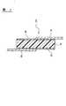
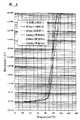
図1は本発明の一実施形態に係るサーミスタ素子を示す概略断面図、図2は図1の平面図、図3および図4は実施例および比較例のサーミスタ素子試料の温度−抵抗(R−T)特性を示すグラフである。
【0027】
サーミスタ素子
図1および図2に示すように、本実施形態に係るサーミスタ素子2は、サーミスタ素体4を有する。サーミスタ素体4の両面には電極6が形成されている。電極6には、外部電極端子8が接続されている。
【0028】
サーミスタ素体
サーミスタ素体4の厚みは通常100〜1000μm程度であり、その材料密度は、2.5g/cm3以上、好ましくは3g/cm3以上であり、その比抵抗は、1Ω−cm以下、好ましくは0.5Ω−cm以下である。
【0029】
サーミスタ素体4は、本発明のPTC組成物で構成してある。本発明のPTC組成物は、少なくとも高分子マトリックスおよび導電性物質を含有する。
【0030】
高分子マトリックス
本発明で用いる高分子マトリックスの融点は、通常70〜200℃であることが好ましい。ただし、低分子有機化合物を併用する場合には、高分子マトリックスの融点は、動作時の低分子有機化合物の融解による流動、素体4の変形等を防ぐため、低分子有機化合物の融点よりも、好ましくは30℃以上、特に好ましくは30℃以上110℃以下の範囲で、高いことが望ましい。
【0031】
本発明で用いる高分子マトリックスは、結晶性でも非晶性でもよく、ポリエチレン、エチレン−酢酸ビニルコポリマー、ポリエチルアクリレート等のポリアルキルアクリレート、ポリメチル(メタ)アクリレート等のポリアルキル(メタ)アクリレート等のポリオレフィン;ポリフッ化ビニリデン、ポリテトラフルオロエチレン、ポリヘキサフルオロプロピレン、これらのコポリマー等のフッ素系ポリマー;ポリ塩化ビニル、ポリ塩化ビニリデン、塩素化ポリ塩化ビニル、塩素化ポリエチレン、塩素化ポリプロピレン、これらのコポリマー等の塩素系ポリマーなどのハロゲン系ポリマー;ポリスチレン、熱可塑性エラストマー等が挙げられる。ポリオレフィンは共重合体であってもよい。中でも、ポリオレフィンを用いることが好ましく、特に好ましくはメタロセン触媒(遷移金属化合物として、主としてメタロセン化合物を用い、有機金属化合物として、主としてメチルアルミノキサンを用いた配位イオン重合触媒)を用いて製造された直鎖状のたとえば密度がたとえば0.95g/cm3未満の低密度ポリエチレンを用いる。
【0032】
メタロセン触媒を用いて製造された直鎖状の低密度ポリエチレンのASTM−D1238で定義されるメルトフローレート(MFR)は、4(g/10分)以下が好ましい。MFRがこれより高いと、溶融粘度が低すぎて、特性の安定性に劣る傾向が見られる。MFRの下限は特にないが、通常0.1(g/10分)程度である。
【0033】
高分子マトリックスは、1種のみを用いても2種以上を併用してもかまわないが、4(g/10分)以下のメタロセン触媒直鎖状低密度ポリエチレンのみを用いることが好ましい。
【0034】
高分子マトリックスの数平均分子量Mnは10000〜50000程度であることが好ましく、より好ましくは18700〜36800程度である。
【0035】
導電性物質
本発明に用いる導電性物質としては、スパイク状の突起を有する導電性粒子を含むことが好ましい。スパイク状の突起を有する導電性粒子は、1個、1個が鋭利な突起をもつ一次粒子から形成されており、粒径の1/3〜1/50の高さの円錘状のスパイク状の突起が1個の粒子に複数(通常10〜500個)存在するものである。その材質は金属、特にNi等が好ましい。
【0036】
このような導電性粒子は、1個、1個が個別に存在する粉体であってもよいが、一次粒子が10〜1000個程度鎖状に連なり二次粒子を形成していることが好ましい。鎖状のものには、一部、一次粒子が存在してもよい。前者の例としては、スパイク状の突起をもつ球状のニッケルパウダがあり、商品名INCO Type 123ニッケルパウダ(インコ社製)として市販されており、その平均粒径は3〜7μm程度、見かけの密度は1.8〜2.7g/cm3程度、比表面積は0.34〜0.44m2/g程度である。
【0037】
また、好ましく用いられる後者の例としては、フィラメント状ニッケル粉があり、商品名INCO Type 210、255、270、287ニッケルパウダ(インコ社製)として市販されており、このうちINCO Type 210、255が特に好ましい。そして、その一次粒子の平均粒径は、好ましくは0.1μm以上、より好ましくは0.5以上4.0μm以下程度である。これらのうち、一次粒子の平均粒径は1.0以上4.0μm以下が最も好ましく、これに平均粒径0.1μm以上1.0μm未満のものを50重量%以下混合してもよい。また、見かけの密度は0.3〜1.0g/cm3程度、比表面積は0.4〜2.5m2/g程度である。なお、平均粒径はフィッシュー・サブシーブ法で測定したものである。
【0038】
このような導電性粒子については、特開平5−47503号公報、米国特許第5378407号明細書に記載されているので参照されたい。
【0039】
また、導電性物質として、スパイク状の突起を有する導電性粒子の他に、カーボンブラック、グラファイト、炭素繊維、金属被覆カーボンブラック、グラファイト化カーボンブラック、金属被覆炭素繊維等の炭素系導電性粒子、球状、フレーク状、繊維状等の金属粒子、異種金属被覆金属(銀コートニッケル等)粒子、炭化タングステン、窒化チタン、窒化ジルコニウム、炭化チタン、ホウ化チタン、ケイ化モリブデン等のセラミック系導電性粒子、また、特開平8−31554号、同9−27383号公報に記載されている導電性チタン酸カリウムウィスカー等を添加してもよい。このような導電性粒子は、スパイク状の突起を有する導電性粒子の25重量%以下とすることが好ましい。
【0040】
低分子有機化合物
本発明では、上述した高分子マトリックスとともに、該高分子マトリックスより融点の低い低分子有機化合物をさらに含有することが好ましい。PTC組成物には、低抵抗かつ高耐熱性の他、低温で動作可能であることが求められることもある。この種の低分子有機化合物を添加することにより、PTC組成物の抵抗−温度特性における動作温度を容易に調整することができる。
【0041】
本発明に用いることができる低分子有機化合物は、分子量1000程度まで、好ましくは200〜800の結晶性物質であり、上述した高分子マトリックスよりも融点mpが低ければ特に制限はないが、常温(25℃程度の温度)で固体であるものが好ましい。
【0042】
低分子有機化合物としては、ワックス(具体的には、パラフィンワックスやマイクロクリスタリンワックス等の石油系ワックス、植物系ワックス、動物系ワックス、鉱物系ワックスのような天然ワックス等)、油脂(具体的には、脂肪または固体脂と称されるもの)、結晶性樹脂などが挙げられる。
【0043】
結晶性樹脂とは、熱測定において融点が観測され得る樹脂を意味し、融点が観測され得ない非晶性樹脂と区別される。結晶性樹脂としては、たとえば直鎖状、又は分岐鎖状の高密度ポリエチレン、低密度ポリエチレン、超高分子量ポリエチレン等のポリエチレン系結晶性樹脂、直鎖状、又は分岐鎖状の高密度ポリプロピレン、低密度ポリプロピレン等のポリプロピレン系結晶性樹脂、および、ポリメチルペンテン、ポリブテン、ポリメチルブテン、ポリメチルヘキセン、ポリビニルナフタレン等からなる群で示されるポリオレフィン系結晶性樹脂や、ポリエチレンテレフタレート(PET)、ポリブチレンテレフタレート(PBT)、ポリエチレンナフタレート、芳香族ポリエステル等からなる群で示されるポリエステル系結晶性樹脂、ナイロン−6、ナイロン−66、ナイロン−12、ポリアミドイミド等からなる群で示されるポリアミド系結晶性樹脂、ポリフッ化ビニリデン、ポリテトラフルオロエチレン等からなる群で示されるフッ素系結晶性樹脂や、その他として、ポリ塩化ビニリデン、ポリアクリロニトリル、シンジオタクチックポリスチレン、ポリオキシメチレン、ポリフェニレンサルファイド(PPS)、ポリエーテルエーテルケトン(PEEK)、セルロース、アセタール樹脂、塩素化ポリエーテル、エチレン−酢酸ビニル共重合体、液晶ポリマー(芳香族多環縮合系ポリマー)等が挙げられる。結晶性樹脂は、全体が結晶化しているもののみではなく、部分的に結晶化しているものも含む。結晶化度は、通常10%以上、好ましくは15%以上であって、通常80%以下、好ましくは70%以下である。
【0044】
たとえば低温(たとえば80〜100℃)動作を目的とする場合には、低分子有機化合物としては、融点mpが40℃以上100℃未満であるものを用いればよい。このようなものとしては、パラフィンワックス、マイクロクリスタリンワックス、脂肪酸、脂肪酸エステル、脂肪酸アミド、結晶性樹脂などが挙げられる。低分子有機化合物は、動作温度等によって1種あるいは2種以上を選択して用いることができる。中でも低分子有機化合物としては、結晶性樹脂が好ましく、より好ましくはエチレンホモポリマー(融点85〜100℃、密度0.96g/cm3程度)を用いる。
【0045】
添加剤
本発明では、高分子マトリックス、および/または該高分子マトリックスの熱劣化を防止するために、酸化防止剤が添加してあってもよい。酸化防止剤としては、フェノール類、有機イオウ類、フォスファイト類(有機リン系)などが用いられる。
【0046】
また、良熱導電性添加物として、特開昭57−12061号公報に記載されている窒化ケイ素、シリカ、アルミナ、粘土(雲母、タルク等)、特公平7−77161号公報に記載されているシリコン、炭化ケイ素、窒化ケイ素、ベリリア、セレン、特開平5−217711号公報に記載されている無機窒化物、酸化マグネシウム等を添加してもよい。
【0047】
耐久性向上のために、特開平5−226112号公報に記載されている酸化チタン、酸化鉄、酸化亜鉛、シリカ、酸化マグネシウム、アルミナ、酸化クロム、硫酸バリウム、炭酸カルシウム、水酸化カルシウム、酸化鉛、特開平6−68963号公報に記載されている高比誘電率の無機固体、具体的には、チタン酸バリウム、チタン酸ストロンチウム、ニオブ酸カリウム等を添加してもよい。
【0048】
耐電圧改善のために、特開平4−74383号公報に記載されている炭化ホウ素等を添加してもよい。
【0049】
強度改善のために、特開平5−74603号公報に記載されている水和チタン酸アルカリ、特開平8−17563号公報に記載されている酸化チタン、酸化鉄、酸化亜鉛、シリカ等を添加してもよい。
【0050】
結晶核剤として、特公昭59−10553号公報に記載されているハロゲン化アルカリ、メラミン樹脂、特開平6−76511号公報に記載されている安息香酸、ジベンジリデンソルビトール、安息香酸金属塩、特開平7−6864号公報に記載されているタルク、ゼオライト、ジベンジリデンソルビトール、特開平7−263127号公報に記載されているソルビトール誘導体(ゲル化剤)、アスファルト、さらには、リン酸ビス(4−t−ブチルフェニル)ナトリウム等を添加してもよい。
【0051】
ア−ク調節制御剤としては、特公平4−28744号公報に記載されているアルミナ、マグネシア水和物、特開昭61−250058号公報に記載されている金属水和物、炭化ケイ素等を添加してもよい。
【0052】
金属害防止剤として、特開平7−6864号公報に記載されているイルガノックスMD1024(チバガイギー製)等を添加してもよい。
【0053】
また、難燃剤として、特開昭61−239581号公報に記載されている三酸化二アンチモン、水酸化アルミニウム、特開平5−74603号公報に記載されている水酸化マグネシウム、さらには、2,2−ビス(4−ヒドロキシ−3,5−ジブロモフェニル)プロパン、ポリフッ化ビニリデン(PVDF)等のハロゲンを含有する有機化合物(重合体を含む)、リン酸アンモニウム等のリン系化合物等を添加してもよい。
【0054】
これら以外にも、硫化亜鉛、塩基性炭酸マグネシウム、酸化アルミニウム、ケイ酸カルシウム、ケイ酸マグネシウム、アルミノシリケート粘土(雲母、タルク、カオリナイト、モンモリロナイト等)、ガラス粉、ガラスフレーク、ガラス繊維、硫酸カルシウム等を添加してもよい。
【0055】
電極
電極6は、Niなどの金属箔などで構成される。電極6の厚みは通常25〜35μm程度である。
【0056】
外部電極端子
外部電極端子8は、Niなどで構成される。外部電極端子8の厚みは通常100〜125μm程度である。
【0057】
サーミスタ素子の製造方法
次に、本実施形態に係るサーミスタ素子2の製造方法を説明する。
【0058】
混練物の作製
まず、少なくとも高分子マトリックスと導電性物質の混練物(混合物)を作製する。混練物を作製するに際して、低分子有機化合物を併用することが好ましい。特に、低温(たとえば80〜100℃程度)で動作させるためには、低分子有機化合物としてエチレンホモポリマーを用いることが好ましい。
【0059】
従来、低温動作可能なPTC組成物は耐熱性が低かったため、外部電極端子のはんだ付けに使用可能なはんだの種類(融点)が限定されており、はんだ付けに不向きであった。しかしながら、高分子マトリックスより融点の低い低分子有機化合物をさらに含有させた混合物を架橋させてPTC組成物とした場合には、低温動作可能でありながら、耐熱性に優れるため、はんだの種類(融点)を限定することなく、外部電極端子をはんだ付けすることができる。
【0060】
低分子有機化合物を併用する場合の、高分子マトリックスと低分子有機化合物の混練比は、重量比で、高分子マトリックス1に対して低分子有機化合物0.05〜0.5倍であることが好ましい。この混練比が小さくなって低分子有機化合物の量が少なくなると、抵抗変化率が十分に得られにくくなる。反対に大きくなって低分子有機化合物の量が多くなると、低分子有機化合物が溶融する際に素体が大きく変形する他、導電性物質との混練が困難になる。
【0061】
高分子マトリックスと低分子有機化合物の合計重量に対する導電性物質の配合比はできるだけ高い方が望ましいが、低抵抗で優れたPTC特性を得るには導電性物質の配合の割合は25〜45体積%であることが好ましい。導電性物質の配合の割合が25体積%に満たない場合、非動作時の室温抵抗を十分低くすることができなくなってくる。また45体積%を越える場合は温度上昇に伴う抵抗値の変化が小さくなり、また、均一な混合が困難になって再現性ある抵抗値が得られにくくなる。
【0062】
また、混練物を作製するに際して、さらに酸化防止剤などの添加剤を添加してもよい。これらの添加剤は、全有機分(高分子マトリックス、低分子有機化合物および導電性物質)の1.0重量%以下となるように添加することが好ましい。
【0063】
高分子マトリックス、導電性物質、および必要に応じて併用される低分子有機化合物や添加剤の混練は、ミル等を用いて、高分子マトリックスの融点以上の温度(好ましくは融点+5〜40℃の温度)で、5〜90分程度行えばよい。また、低分子有機化合物を併用する場合には、予め高分子マトリックスと低分子有機化合物とを溶融混合または溶媒中で溶解し混練してもよい。
【0064】
成形物の作製
次に、混練物(混合物)の両面を電極材料で挟み、圧着して厚み300〜350μm程度のシート状またはフィルム状の成形物(混合物)を作製する。電極材料としては、Niなどの金属箔などが使用可能である。その厚みは25〜35μm程度である。圧着は、たとえば熱プレス機を用いて、130〜240℃程度の温度で行うことができる。
【0065】
架橋成形物の作製
次に、成形物(混合物)に電子線を照射し、当該成形物を架橋させて架橋成形物(組成物)を作製する。本実施形態では、架橋前の成形物に、加速電圧が250KV以上、好ましくは1000KV以上の電子加速器を用いて電子線を、40〜300KGy、好ましくは40〜200KGyの照射量で照射し、当該成形物を架橋させる。電子線の照射は、成形物の温度上昇を70℃以下(特に60℃以下)かつ混合物を変形させない温度に抑制可能な照射量で、複数回に分けて行うことが好ましい。このような照射量はたとえば40KGy以下、好ましくは20KGy以下である。たとえば40KGy以上の照射を望む場合、1回の照射量をたとえば20KGyとし、これを複数回に分けて行うことが好ましい。さらに好ましくは、前記電子線の照射を前記混合物の両面に行う。
【0066】
なお、混練物(混合物)からシート状またはフィルム状の成形物(混合物)を作製し、当該成形物に電子線を照射し、架橋させて架橋成形物(組成物)を作製した後、その両面に電極材料を形成してもよい。
【0067】
外部電極端子の接合
次に、架橋成形物(組成物)を所定形状に打ち抜きあるいはカットした後、電極6の表面に、外部電極端子8を接合してサーミスタ素子2とする。
【0068】
外部電極端子8の接合は、鉛レスで250℃以下(好ましくは220℃以下)の液相線を有するはんだを用いて行うことが好ましい。外部電極端子8のはんだ付けは、たとえばリフローあるいは、こてやホットプレートなどを用いて行うことができる。
【0069】
作用
本実施形態に係るサーミスタ素子2の製造方法によると、混合物の両面を電極材料で挟み、圧着して得られるシート状またはフィルム状の成形物に、特定の電子線を特定量照射して架橋させる。このため、成形物の材料密度が高く、電極を含む厚みが厚い場合でも、成形物を均一に架橋させることが可能である。その結果、低抵抗(たとえば一対の電極間で測定される比抵抗が1Ω−cm以下)で耐熱性に優れたサーミスタ素子2を得ることができる。また、照射対象の成形物の厚みが厚くても、成形物を均一に架橋させることが可能であるから、得られるサーミスタ素子2の耐圧も向上する。
【0070】
また、加速電圧が高い電子加速器を用いて電子線を照射する場合、一回の照射量が多くなると、混合物の温度上昇が著しくなり、変形を生じることがある。そこで、電子線の照射を、前記混合物の温度上昇を70℃以下かつ混合物を変形させない温度に抑制可能な照射量(たとえば40KGy以下)で複数回に分けて行うことにより、混合物を変形させることなく、均一に架橋させることが可能となる。その結果、熱安定性が高く、熱衝撃特性などの信頼性に優れたサーミスタ素子2とすることができる。
【0071】
さらに、電子線の照射を、成形物の両面に行うことにより、一層均一に成形物を架橋させることが可能となり、耐熱性が高度に安定する。
【0072】
その他の実施形態
以上、本発明の実施形態について説明してきたが、本発明はこうした実施形態に何等限定されるものではなく、本発明の要旨を逸脱しない範囲内において種々なる態様で実施し得ることは勿論である。
【0073】
たとえば、上述した実施形態では、一枚の成形物(混合物)に電子線を照射し、架橋させて一枚の架橋成形物(組成物)を作製することとしているが、複数枚の成形物を重ねた積層体に、加速電圧が1000KV以上(好ましくは2000KV以上)の電子加速器を用いて電子線を照射することも好ましい。加速電圧を高くして電子線を照射することにより、複数枚の成形物を1回の照射で架橋させることが可能となる。その結果、一回の処理量が増加し、大幅なコストダウンが期待できる。
【0074】
加速電圧を高くすればするほど、これに比例して電子線の透過能力も向上する。したがって、たとえば3枚の成形物を重ねた積層体(厚み1000μm程度)に、加速電圧がたとえば1000KVの電子加速器を用いて電子線を照射する場合に、その照射量は40〜300KGy程度であることが好ましい。ただし、複数枚の成形物を重ねた積層体に電子線を照射する場合でも、上述した実施形態と同様に、1回の照射量を少なくしてこれを複数回行ってもよく、あるいはさらに前記電子線の照射を前記積層体の両面に行うこととしてもよい。
【0075】
【実施例】
以下、本発明を、さらに詳細な実施例に基づき説明するが、本発明はこれら実施例に限定されない。
【0076】
実施例1
高分子マトリックスとしてのメタロセン触媒による直鎖状の低密度ポリエチレン(融点122℃、比重0.93)57体積%および低分子有機化合物としてのエチレンホモポリマー(融点99℃)8体積%に、導電粒子としてのスパイク状の突起を有するフィラメント状ニッケル粉(平均粒径0.5〜1.0μm)を35体積%となるように添加し、さらにフェノール系およびイオウ系酸化防止剤を、全有機分の0.5重量%となるように添加した後、150℃に加熱しながらミル中で30分間、加熱混練して混練物を得た。
【0077】
得られた混練物の両面を厚さ25μmのNi箔で挟み、熱プレス機で150℃で混練物とNi箔を圧着し、電極を含む厚みが300μmの成形物を得た。
【0078】
得られた成形物の両面に、加速電圧が2000KVの電子加速器を用いて電子線を40KGyの照射量で一度に照射し、9mm、幅3.6mmの角型に打ち抜いた後、これに0.1mm厚のNi端子板を両主面に鉛レス低温はんだ(液相線204℃)ではんだ付けしてサーミスタ素子試料を得た。これと同一の試料を3つ作製した。得られた試料について以下の評価した。
【0079】
評価項目としては、第1に、200℃の熱板(ホットプレート)上に5分間、試料を放置し、素体の変形があるかどうかを観察した。
【0080】
第2に、一部のサンプルついては架橋度の目安として電極を剥離してゲル分率を測定した。ゲル分率はトルエンで試料を煮沸後、濾過し、全体の重量に対する濾過できずに残留したゲル分の重量の割合によって計算した。架橋度が上がるとゲル分率は上がることになる。
【0081】
第3に、抵抗温度特性(R−T特性)および熱衝撃特性(−40℃〜+85℃、各30分安定、200∞)を評価した。R−T特性については、試料を、恒温槽内で加熱し、所定の温度で、4端子法で抵抗値を測定して温度−抵抗曲線を得た。この結果を図3に示す。室温(25℃)抵抗値は8.5×10⁻³Ω(0.089Ω−cm)程度で、90℃付近で抵抗の急激な上昇が見られ、最大抵抗値は1×10⁹Ω超(1×10¹⁰Ω−cm超)となり、抵抗変化率は11.1桁超であった。これらの結果を表1に示す。
【0082】
実施例2
電子線の照射量を100KGyにし、これを20KGyずつの5回に分けて照射した以外は、実施例1と同様にして試料を作製し、同様の評価を行った。また、実施例1と同様に、得られた試料の温度−抵抗曲線を図3に示す。室温(25℃)抵抗値は9.3×10⁻³Ω(0.094Ω−cm)程度で、90℃付近で抵抗の急激な上昇が見られ、最大抵抗値は1×10⁹Ω超(1×10¹⁰Ω−cm超)となり、抵抗変化率は11桁超であった。結果を表1に示す。
【0083】
実施例3
電子線の照射量を200KGyにし、これを20KGyずつの10回に分けて照射した以外は、実施例1と同様にして試料を作製し、同様の評価を行った。また、実施例1と同様に、得られた試料の温度−抵抗曲線を図3に示す。室温(25℃)抵抗値は9.5×10⁻³Ω(0.096Ω−cm)程度で、85℃付近で抵抗の急激な上昇が見られ、最大抵抗値は1×10⁹Ω超(1×10¹⁰Ω−cm超)となり、抵抗変化率は11桁超であった。結果を表1に示す。
【0084】
実施例4
電子線の照射量を300KGyにし、これを20KGyずつの15回に分けて照射した以外は、実施例1と同様にして試料を作製し、同様の評価を行った。また、実施例1と同様に、得られた試料の温度−抵抗曲線を図3に示す。室温(25℃)抵抗値は8.5×10⁻³Ω(0.086Ω−cm)程度で、80℃付近で抵抗の急激な上昇が見られ、最大抵抗値は1×10⁹Ω超(1×10¹⁰Ω−cm超)となり、抵抗変化率は11.1桁超であった。結果を表1に示す。
【0085】
実施例5
ニッケル粉の添加量を30体積%とし、電子線の加速電圧を250KVとし、照射量を200KGyとして一度に照射し、端子はんだ付けを行わなかった以外は、実施例1と同様にして試料を作製し、同様の評価を行った。結果を表1に示す。
【0086】
実施例6
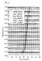
ニッケル粉の添加量を30体積%とし、端子はんだ付けを行わなかった以外は、実施例1と同様にして試料を作製し、同様の評価を行った。また、実施例1と同様に、得られた試料の温度−抵抗曲線を図4に示す。室温(25℃)抵抗値は5×10⁻⁴Ω(5.1×10⁻³Ω−cm)程度で、85℃付近で抵抗の急激な上昇が見られ、最大抵抗値は4.5×10⁷Ω超(4.5×10⁸Ω−cm超)となり、抵抗変化率は11桁超であった。結果を表1に示す。
【0087】
実施例7
電子線の照射量を100KGyにし、これを20KGyずつの5回に分けて照射した以外は、実施例6と同様にして試料を作製し、同様の評価を行った。また、実施例1と同様に、得られた試料の温度−抵抗曲線を図4に示す。室温(25℃)抵抗値は5×10⁻⁴Ω(5.1×10⁻³Ω−cm)程度で、85℃付近で抵抗の急激な上昇が見られ、最大抵抗値は3.5×10⁷Ω超(3.5×10⁸Ω−cm)となり、抵抗変化率は10.8桁超であった。結果を表1に示す。
【0088】
比較例1(未架橋)
電子線の照射を行わず(未架橋)、かつ端子はんだ付けを行わなかった以外は、実施例1と同様にして試料を作製し、同様の評価を行った。また、実施例1と同様に、得られた試料の温度−抵抗曲線を図3に示す。室温(25℃)抵抗値は1.1×10⁻²Ω(1.1×10⁻¹Ω−cm)程度で、95℃付近で抵抗の急激な上昇が見られ、最大抵抗値は6.4×10⁷Ω超(6.4×10⁸Ω−cm)となり、抵抗変化率は9.8桁超であった。結果を表1に示す。
【0089】
比較例2(未架橋)
ニッケル粉の添加量を30体積%とした以外は、比較例1と同様にして試料を作製し、同様の評価を行った。また、実施例1と同様に、得られた試料の温度−抵抗曲線を図4に示す。室温(25℃)抵抗値は5×10⁻⁴Ω(5.1×10⁻³Ω−cm)程度で、80℃付近で抵抗の急激な上昇が見られ、最大抵抗値は1.1×10⁷Ω超(1.1×10⁸Ω−cm超)となり、抵抗変化率は11.2桁超であった。結果を表1に示す。
【0090】
比較例3(照射線量が過小)
電子線の照射量を20KGyにした以外は、実施例1と同様にして試料を作製し、同様の評価を行った。また、実施例1と同様に、得られた試料の温度−抵抗曲線を図3に示す。室温(25℃)抵抗値は8.8×10⁻³Ω(8.9×10⁻²Ω−cm)程度で、90℃付近で抵抗の急激な上昇が見られ、最大抵抗値は1×10⁹Ω超(1×10¹⁰Ω−cm超)となり、抵抗変化率は11.1桁超であった。結果を表1に示す。
【0091】
比較例4(照射線量が過小)
ニッケル粉の添加量を30体積%とし、端子はんだ付けを行わなかった以外は、比較例2と同様にして試料を作製し、同様の評価を行った。また、実施例1と同様に、得られた試料の温度−抵抗曲線を図4に示す。室温(25℃)抵抗値は5×10⁻⁴Ω(5.1×10⁻³Ω−cm)程度で、80℃付近で抵抗の急激な上昇が見られ、最大抵抗値は1.1×10⁷Ω超(1.1×10⁸Ω−cm超)となり、抵抗変化率は10.3桁超であった。結果を表1に示す。
【0092】
比較例5(照射線量が過大)
電子線の照射量を400KGyにした以外は、実施例1と同様にして試料を作製し、同様の評価を行った。また、実施例1と同様に、得られた試料の温度−抵抗曲線を図4に示す。室温(25℃)抵抗値は5×10⁻⁴Ω(5.1×10⁻³Ω−cm)程度で、70℃付近で抵抗の急激な上昇が見られ、最大抵抗値は7.9×10⁵Ω超(7.4×10⁶Ω−cm超)となり、抵抗変化率は9.2桁超であった。結果を表1に示す。
【0093】
比較例6(加速電圧が過小)
電子線の加速電圧を200KVとした以外は、実施例1と同様にして試料を作製し、同様の評価を行った。また、実施例1と同様に、得られた試料の温度−抵抗曲線を図4に示す。室温(25℃)抵抗値は5×10⁻⁴Ω(5.1×10⁻³Ω−cm)程度で、80℃付近で抵抗の急激な上昇が見られ、最大抵抗値は9×10⁷Ω超(9.1×10⁸Ω−cm超)となり、抵抗変化率は11.3桁超であった。結果を表1に示す。
【0094】
【表1】
表1から以下のことが理解される。まず、加速電圧が250KVの両面照射では、耐熱性が改善されることが確認できた(実施例5)。これは、一般に電子線は物質を通過する際に減衰するため、片面照射だけでは架橋度のムラが生じ易いことに起因し、この傾向は加速電圧が低いほど顕著に現れる傾向がある。しかし、このような低加速電圧でも素体の両面に照射することで架橋度の均一性がアップし、耐熱性が改善されるものと考える。加速電圧が2000KVでは、材質によって傾向が異なるが、電子線の透過力がアップするため片面照射だけでも耐熱性が改善されることが確認できた(実施例1〜4,6,7)。
【0096】
次に、材料密度が3.3g/cm3 の試料(実施例5〜7、比較例2,4、参考例2〜3)では、20KGy未満の照射量では素体の変形があり好ましくない(比較例2,4)。優れたPTC特性としては、R−T桁が大きいほどよく(好ましくは5桁以上)、実施例では、照射量40〜200KGyの範囲が、耐熱に優れたPTC特性が得られる照射範囲といえる(実施例5〜7)。材料密度3.7g/cm3 の試料(実施例1〜4、比較例1,3)では、同様に20KGy未満の照射量は耐熱性が悪く好ましくない(比較例1,3)。40KGy以上では耐熱性に優れたPTC特性が得られている(実施例1,2)。ただし、原因は不明だが、200KGy以上でR−Tの立ち上がりが、低温シフトする傾向があり、これに起因して熱衝撃性が若干悪くなる傾向が認められた(実施例3,4)。
【0097】
次に、照射線量が400KGyと過大になると、R−T特性が低温側にシフトし、熱衝撃特性が低下する傾向が確認された(比較例5)。
【0098】
次に、加速電圧が200KVと過小になると、ゲル分率が測定できないほど低く、耐熱試験での素体の変形が確認された(比較例6)。
【図面の簡単な説明】
【図1】 図1は本発明の一実施形態に係るサーミスタ素子を示す概略断面図である。
【図2】 図2は図1の平面図である。
【図3】 図3は実施例および比較例のサーミスタ素子試料の温度−抵抗(R−T)特性を示すグラフである。
【図4】 図4は実施例および比較例のサーミスタ素子試料の温度−抵抗(R−T)特性を示すグラフである。
【符号の説明】
2… サーミスタ素子
4… サーミスタ素体(PTC組成物)
6… 電極
8… 外部電極端子[0001]
BACKGROUND OF THE INVENTION
The present invention is used as a temperature sensor or an overcurrent protection element, and has a positive temperature coefficient of positive temperature coefficient (hereinafter abbreviated as PTC) characteristic and a thermistor element having a resistance value that increases as the temperature rises. The present invention relates to these manufacturing methods.
[0002]
[Prior art]
It is known that a composition in which a conductive substance is dispersed in a crystalline polymer matrix exhibits PTC behavior (see US Pat. Nos. 3,243,753 and 3,351,882). However, this conventional PTC composition has a problem that stability during storage and heat resistance are low.
[0003]
Thus, it has been studied to improve the storage stability and heat resistance of the PTC composition by crosslinking the crystalline polymer matrix (US Pat. No. 3,269,862 and JP-A-2000-82602). reference).
[0004]
Known crosslinking methods include chemical crosslinking treatment with an organic peroxide, water crosslinking treatment with a silane coupling agent and water, and radiation crosslinking treatment with electron beam irradiation.
[0005]
However, in the chemical cross-linking treatment, since the composition must be molded into a molded body having a predetermined shape and then heat-treated at a temperature higher than the melting point of the polymer matrix contained in the composition, the shape of the molded body is maintained. There is a problem that it is difficult to perform the heat treatment and the molded body may be thermally deteriorated.
[0006]
In addition, in the water cross-linking treatment, there are many variations in the cross-linking effect, it is necessary to immerse in warm water for a long time, the process becomes long, and a substance that can affect the environment such as organic tin must be used as a catalyst. There were problems such as not becoming.
[0007]
In contrast, in the radiation cross-linking treatment, carbon black is used as the conductive powder and the density is relatively low (for example, 2.5 g /
[0008]
[Problems to be solved by the invention]
However, the radiation crosslinking has a problem that uniform crosslinking cannot be achieved when the density of the composition is high or the thickness is large. If the crosslinking cannot be performed uniformly, the heat resistance is not sufficiently improved.
[0009]
The object of the present invention is to achieve a high material density (for example a material density of 2.5 g / cm3And a thermistor element having low resistance (specific resistance is, for example, 1 Ω-cm or less), thermistor elements, and methods for producing them.
[0010]
[Means for Solving the Problems]
In order to achieve the above object, the PTC composition according to the present invention comprises at leastMade of linear low density polyethyleneA mixture containing a polymer matrix and a conductive substance is irradiated with an electron beam at an irradiation dose of 40 to 300 KGy (more preferably 40 to 200 KGy) using an electron accelerator having an acceleration voltage of 250 KV or more, and the mixture is crosslinked. It is characterized by being obtained.
[0011]
The method for producing a PTC composition according to the present invention comprises at leastMade of linear low density polyethyleneThe mixture containing a polymer matrix and a conductive substance is irradiated with an electron beam at an irradiation dose of 40 to 300 KGy using an electron accelerator having an acceleration voltage of 250 KV or more to crosslink the mixture.
[0012]
The term mixture in the present specification includes not only a kneaded product, but also a molded product obtained by molding the kneaded product into a sheet or film, and an embodiment in which electrodes are formed on both surfaces of the molded product. Shall. The composition means a crosslinked product of the mixture.
[0013]
In the present invention,Linear low density polyethylene, Produced using metallocene catalystTo be donepreferable. The conductive material preferably includes a filamentary nickel powder having spike-like protrusions on the surface.
[0014]
In the present invention, the mixture before the electron beam irradiation is at leastMade of linear low density polyethyleneIt only needs to contain a polymer matrix and a conductive material, but it is preferable to further contain a low molecular organic compound having a melting point lower than that of the polymer matrix. In particular, in order to operate at a low temperature (for example, about 80 to 100 ° C.), it is preferable to use an ethylene homopolymer as the low molecular weight organic compound.
[0015]
In the present invention, the electron beam irradiation is performed at a temperature of the mixture.Rise70 ° C or lessAnd the temperature at which the mixture does not deformIt is preferable to divide the dose into a plurality of times with a dose that can be suppressed to a minimum.
[0016]
In the present invention, more preferably, the electron beam irradiation is performed on both surfaces of the mixture.
[0017]
In this invention, it is preferable to irradiate an electron beam using the electron accelerator whose acceleration voltage is 1000 KV or more to the laminated body which piled up the said several said mixture.
[0018]
The thermistor element according to the present invention is characterized in that electrodes are formed on both sides of a thermistor body made of the above-described PTC composition. It is preferable that the external electrode terminal is connected to the surface of each electrode with lead-free solder having a liquidus of 250 ° C. or less.
[0019]
The thermistor element manufacturing method according to the present invention includes at leastMade of linear low density polyethyleneAfter electrodes are formed on both surfaces of a molded product formed into a sheet or film using a kneaded material containing a polymer matrix and a conductive material, an electron beam is emitted from an electron beam of 40 to 40 using an electron accelerator having an acceleration voltage of 250 KV or more. Irradiation is performed at a dose of 300 KGy to crosslink the molded product. After cross-linking the molded product, it is preferable to connect an external electrode terminal to the surface of each electrode using a lead-free solder having a liquidus of 250 ° C. or lower.
Examples of the thermistor element include a self-control heating element, an overcurrent protection element, and a temperature sensor.
[0020]
Operation and effect of the invention
In recent years, low resistance, low temperature (80 to 100 ° C.) operation, and high heat resistance PTC compositions are required for use in Li-ion batteries typified by mobile phones and protective elements for general-purpose circuits.
[0021]
According to the present invention, the mixture is crosslinked by irradiation with a specific amount of a specific electron beam. For this reason, the material density of the mixture is, for example, 2.5 g / cm.3Even when the thickness including the electrode is high, for example, 200 μm or more, the mixture can be uniformly crosslinked. As a result, a PTC composition having low resistance (for example, a specific resistance measured between a pair of electrodes of 1 Ω-cm or less) and excellent heat resistance, and a thermistor element using the PTC composition can be provided. Further, even if the mixture to be irradiated is thick, it is possible to uniformly crosslink the mixture. Therefore, the withstand voltage of the obtained PTC composition and the thermistor element using the same is improved.
[0022]
Moreover, when irradiating an electron beam using an electron accelerator with an acceleration voltage as high as 1000 KV or more, for example, if the amount of irradiation at one time increases, the temperature of the mixture increases significantly and deformation may occur. In such a case, the electron beam irradiation is performed at the temperature of the mixture.Rise70 ° C or lessAnd the temperature at which the mixture does not deformBy performing the treatment in a plurality of times with an irradiation dose that can be suppressed to 40 kgy or less (for example, 40 KGy or less), the mixture can be uniformly crosslinked without being deformed. As a result, a PTC composition having high thermal stability and excellent reliability such as thermal shock characteristics can be obtained.
[0023]
Further, by irradiating both surfaces of the mixture with electron beams, the mixture can be more uniformly cross-linked, and the heat resistance is highly stable.
[0024]
In the present invention, when the acceleration voltage of the electron accelerator to be used is increased, the transmission ability of the electron beam to the irradiation target is also improved. That is, by increasing the acceleration voltage, it is possible to crosslink a plurality of the mixtures by one irradiation. As a result, the amount of processing at one time increases, and a significant cost reduction can be expected.
[0025]
DETAILED DESCRIPTION OF THE INVENTION
Embodiments of the present invention will be described below with reference to the drawings.
[0026]
1 is a schematic cross-sectional view showing a thermistor element according to an embodiment of the present invention, FIG. 2 is a plan view of FIG. 1, and FIGS. 3 and 4 are temperature-resistance (R-) of thermistor element samples of Examples and Comparative Examples. T) is a graph showing characteristics.
[0027]
Thermistor element
As shown in FIGS. 1 and 2, the
[0028]
Thermistor body
The thickness of the
[0029]
The
[0030]
Polymer matrix
The melting point of the polymer matrix used in the present invention is usually preferably 70 to 200 ° C. However, when the low molecular organic compound is used in combination, the melting point of the polymer matrix is higher than the melting point of the low molecular organic compound in order to prevent the flow due to melting of the low molecular organic compound during operation, deformation of the
[0031]
The polymer matrix used in the present invention may be crystalline or amorphous, such as polyethylene, ethylene-vinyl acetate copolymer, polyalkyl acrylate such as polyethyl acrylate, polyalkyl (meth) acrylate such as polymethyl (meth) acrylate, etc. Polyolefins; Fluoropolymers such as polyvinylidene fluoride, polytetrafluoroethylene, polyhexafluoropropylene, and copolymers thereof; polyvinyl chloride, polyvinylidene chloride, chlorinated polyvinyl chloride, chlorinated polyethylene, chlorinated polypropylene, and copolymers thereof And halogen-based polymers such as chlorinated polymers such as polystyrene and thermoplastic elastomers. The polyolefin may be a copolymer. Among them, it is preferable to use polyolefin, and particularly preferably, it is a catalyst prepared directly using a metallocene catalyst (coordination ion polymerization catalyst mainly using a metallocene compound as a transition metal compound and mainly methylaluminoxane as an organometallic compound). For example, the chain has a density of, for example, 0.95 g / cm3Less than low density polyethylene is used.
[0032]
The melt flow rate (MFR) defined by ASTM-D1238 of a linear low density polyethylene produced using a metallocene catalyst is preferably 4 (g / 10 min) or less. When MFR is higher than this, the melt viscosity is too low, and the tendency of inferior property stability is observed. The lower limit of MFR is not particularly limited, but is usually about 0.1 (g / 10 minutes).
[0033]
The polymer matrix may be used alone or in combination of two or more, but it is preferable to use only metallocene-catalyzed linear low density polyethylene of 4 (g / 10 min) or less.
[0034]
The number average molecular weight Mn of the polymer matrix is preferably about 10,000 to 50,000, more preferably about 18700 to 36800.
[0035]
Conductive material
The conductive substance used in the present invention preferably includes conductive particles having spike-like protrusions. The conductive particles having spike-shaped protrusions are formed of primary particles each having a sharp protrusion, and a cone-shaped spike shape having a height of 1/3 to 1/50 of the particle diameter. Are present in a plurality of particles (usually 10 to 500). The material is preferably a metal, particularly Ni.
[0036]
Such conductive particles may be a powder in which one particle or one particle exists individually, but it is preferable that about 10 to 1000 primary particles are connected in a chain to form secondary particles. . A part of the chain may have primary particles. As an example of the former, there is a spherical nickel powder having spike-like protrusions, which is commercially available as a trade name INCO Type 123 nickel powder (manufactured by Inco), whose average particle diameter is about 3 to 7 μm, apparent density Is 1.8 to 2.7 g / cm3Degree, specific surface area is 0.34-0.44m2/ G or so.
[0037]
Examples of the latter that is preferably used include filamentary nickel powder, which is commercially available under the trade name INCO Type 210, 255, 270, 287 Nickel Powder (manufactured by Inco), of which INCO Type 210, 255 is Particularly preferred. And the average particle diameter of the primary particle becomes like this. Preferably it is 0.1 micrometer or more, More preferably, it is about 0.5 or more and 4.0 micrometers or less. Of these, the average particle size of the primary particles is most preferably 1.0 or more and 4.0 μm or less, and those having an average particle size of 0.1 μm or more and less than 1.0 μm may be mixed with 50% by weight or less. The apparent density is 0.3 to 1.0 g / cm.3Degree, specific surface area is 0.4-2.5m2/ G or so. The average particle diameter is measured by the fish-subsieve method.
[0038]
Such conductive particles are described in JP-A-5-47503 and US Pat. No. 5,378,407, so please refer to them.
[0039]
In addition to conductive particles having spike-like projections as conductive substances, carbon-based conductive particles such as carbon black, graphite, carbon fiber, metal-coated carbon black, graphitized carbon black, metal-coated carbon fiber, Ceramic conductive particles such as spherical, flaky, fibrous, etc. metal particles, dissimilar metal-coated metal (silver coated nickel, etc.) particles, tungsten carbide, titanium nitride, zirconium nitride, titanium carbide, titanium boride, molybdenum silicide, etc. Moreover, you may add the electroconductive potassium titanate whisker etc. which are described in Unexamined-Japanese-Patent No. 8-31554, 9-27383. Such conductive particles are preferably 25% by weight or less of the conductive particles having spike-like protrusions.
[0040]
Low molecular weight organic compounds
In the present invention, it is preferable to further contain a low molecular organic compound having a melting point lower than that of the polymer matrix together with the polymer matrix described above. In addition to low resistance and high heat resistance, the PTC composition may be required to be operable at a low temperature. By adding this kind of low molecular weight organic compound, the operating temperature in the resistance-temperature characteristics of the PTC composition can be easily adjusted.
[0041]
The low molecular weight organic compound that can be used in the present invention is a crystalline substance having a molecular weight of up to about 1000, preferably 200 to 800, and is not particularly limited as long as the melting point mp is lower than the above-described polymer matrix. Those which are solid at a temperature of about 25 ° C. are preferred.
[0042]
Low molecular organic compounds include waxes (specifically, petroleum waxes such as paraffin wax and microcrystalline wax, natural waxes such as plant waxes, animal waxes and mineral waxes), fats and oils (specifically Are fats or solid fats), crystalline resins and the like.
[0043]
The crystalline resin means a resin whose melting point can be observed in thermal measurement, and is distinguished from an amorphous resin whose melting point cannot be observed. Examples of the crystalline resin include linear or branched high-density polyethylene, low-density polyethylene, ultra-high molecular weight polyethylene and other polyethylene-based crystalline resins, linear or branched high-density polypropylene, low Polypropylene crystalline resins such as density polypropylene, and polyolefin crystalline resins represented by the group consisting of polymethylpentene, polybutene, polymethylbutene, polymethylhexene, polyvinyl naphthalene, polyethylene terephthalate (PET), polybutylene Polyester crystalline resin shown in the group consisting of terephthalate (PBT), polyethylene naphthalate, aromatic polyester, etc., Polyamide crystalline shown in the group consisting of nylon-6, nylon-66, nylon-12, polyamideimide, etc. Resin, plastic Fluorine-based crystalline resins represented by the group consisting of vinylidene fluoride, polytetrafluoroethylene, and the like, and others include polyvinylidene chloride, polyacrylonitrile, syndiotactic polystyrene, polyoxymethylene, polyphenylene sulfide (PPS), polyether ether Examples include ketone (PEEK), cellulose, acetal resin, chlorinated polyether, ethylene-vinyl acetate copolymer, liquid crystal polymer (aromatic polycyclic condensation polymer), and the like. The crystalline resin includes not only those that are entirely crystallized, but also those that are partially crystallized. The degree of crystallinity is usually 10% or more, preferably 15% or more, and usually 80% or less, preferably 70% or less.
[0044]
For example, when aiming at low temperature (for example, 80 to 100 ° C.) operation, a low molecular organic compound having a melting point mp of 40 ° C. or more and less than 100 ° C. may be used. Examples of such materials include paraffin wax, microcrystalline wax, fatty acid, fatty acid ester, fatty acid amide, and crystalline resin. One or more low molecular organic compounds can be selected and used depending on the operating temperature. Among them, as the low molecular organic compound, a crystalline resin is preferable, and an ethylene homopolymer (melting point: 85 to 100 ° C., density: 0.96 g / cm 3 is more preferable.3Degree).
[0045]
Additive
In the present invention, an antioxidant may be added in order to prevent thermal degradation of the polymer matrix and / or the polymer matrix. As the antioxidant, phenols, organic sulfurs, phosphites (organic phosphorus type), and the like are used.
[0046]
Further, as good heat conductive additives, silicon nitride, silica, alumina, clay (mica, talc, etc.) described in JP-A-57-12061, and JP-B-7-77161 are described. Silicon, silicon carbide, silicon nitride, beryllia, selenium, inorganic nitrides described in JP-A-5-217711, magnesium oxide, and the like may be added.
[0047]
To improve durability, titanium oxide, iron oxide, zinc oxide, silica, magnesium oxide, alumina, chromium oxide, barium sulfate, calcium carbonate, calcium hydroxide, lead oxide described in JP-A-5-226112 Inorganic solids having a high relative dielectric constant described in JP-A-6-68963, specifically, barium titanate, strontium titanate, potassium niobate and the like may be added.
[0048]
For improving the withstand voltage, boron carbide or the like described in JP-A-4-74383 may be added.
[0049]
In order to improve the strength, hydrated alkali titanate described in JP-A-5-74603, titanium oxide, iron oxide, zinc oxide, silica, etc. described in JP-A-8-17563 are added. May be.
[0050]
Examples of the crystal nucleating agent include alkali halides and melamine resins described in JP-B-59-10553, benzoic acid, dibenzylidene sorbitol, metal benzoate described in JP-A-6-76511, Talc, zeolite, dibenzylidene sorbitol described in JP-A-7-6864, sorbitol derivatives (gelling agents) described in JP-A-7-263127, asphalt, and bis (4-t -Butylphenyl) sodium and the like may be added.
[0051]
Examples of the arc control agent include alumina, magnesia hydrate described in JP-B-4-28744, metal hydrate described in JP-A-61-250058, silicon carbide, and the like. It may be added.
[0052]
Irganox MD1024 (manufactured by Ciba Geigy) and the like described in JP-A-7-6864 may be added as a metal harm prevention agent.
[0053]
Examples of the flame retardant include antimony trioxide, aluminum hydroxide described in JP-A-61-239581, magnesium hydroxide described in JP-A-5-74603, and 2,2 -Add halogen-containing organic compounds (including polymers) such as bis (4-hydroxy-3,5-dibromophenyl) propane, polyvinylidene fluoride (PVDF), phosphorus-based compounds such as ammonium phosphate, etc. Also good.
[0054]
Other than these, zinc sulfide, basic magnesium carbonate, aluminum oxide, calcium silicate, magnesium silicate, aluminosilicate clay (mica, talc, kaolinite, montmorillonite, etc.), glass powder, glass flakes, glass fiber, calcium sulfate Etc. may be added.
[0055]
electrode
The
[0056]
External electrode terminal
The
[0057]
Method for manufacturing thermistor element
Next, a method for manufacturing the
[0058]
Preparation of kneaded material
First, a kneaded mixture (mixture) of at least a polymer matrix and a conductive substance is prepared. In preparing the kneaded product, it is preferable to use a low molecular organic compound in combination. In particular, in order to operate at a low temperature (for example, about 80 to 100 ° C.), it is preferable to use an ethylene homopolymer as the low molecular weight organic compound.
[0059]
Conventionally, since PTC compositions that can be operated at low temperatures have low heat resistance, the types (melting points) of solder that can be used for soldering external electrode terminals are limited, and are not suitable for soldering. However, when a mixture containing a low molecular weight organic compound having a lower melting point than that of the polymer matrix is crosslinked to form a PTC composition, it is possible to operate at a low temperature but has excellent heat resistance. The external electrode terminal can be soldered without limiting.
[0060]
When the low molecular organic compound is used in combination, the kneading ratio of the polymer matrix and the low molecular organic compound is 0.05 to 0.5 times the weight of the low molecular organic compound relative to the
[0061]
The ratio of the conductive material to the total weight of the polymer matrix and the low molecular organic compound is preferably as high as possible. However, in order to obtain excellent PTC characteristics with low resistance, the ratio of the conductive material is 25 to 45% by volume. It is preferable that When the proportion of the conductive material is less than 25% by volume, the room temperature resistance during non-operation cannot be sufficiently reduced. On the other hand, if it exceeds 45% by volume, the change in the resistance value with increasing temperature becomes small, and uniform mixing becomes difficult, making it difficult to obtain a reproducible resistance value.
[0062]
Moreover, when preparing a kneaded material, you may add additives, such as antioxidant, further. These additives are preferably added so as to be 1.0% by weight or less of the total organic content (polymer matrix, low molecular organic compound and conductive substance).
[0063]
The kneading of the polymer matrix, the conductive material, and the low-molecular organic compound or additive used in combination as necessary is performed at a temperature equal to or higher than the melting point of the polymer matrix (preferably a melting point +5 to 40 ° C.) using a mill or the like. Temperature) for about 5 to 90 minutes. When a low molecular organic compound is used in combination, the polymer matrix and the low molecular organic compound may be previously melt-mixed or dissolved in a solvent and kneaded.
[0064]
Molding production
Next, both surfaces of the kneaded product (mixture) are sandwiched between electrode materials and pressed to produce a sheet-like or film-like molded product (mixture) having a thickness of about 300 to 350 μm. A metal foil such as Ni can be used as the electrode material. Its thickness is about 25 to 35 μm. The pressure bonding can be performed at a temperature of about 130 to 240 ° C. using a hot press machine, for example.
[0065]
Production of cross-linked molding
Next, the molded product (mixture) is irradiated with an electron beam to crosslink the molded product to produce a crosslinked molded product (composition). In this embodiment, the molded product before crosslinking is irradiated with an electron beam at an irradiation dose of 40 to 300 KGy, preferably 40 to 200 KGy, using an electron accelerator having an acceleration voltage of 250 KV or more, preferably 1000 KV or more. Cross-link the product. Electron beam irradiation is the temperature of the molded productRise70 degrees C or less (especially 60 degrees C or less)And the temperature at which the mixture does not deformIt is preferable to divide the dose into a plurality of times with a dose that can be suppressed to a minimum. Such an irradiation amount is, for example, 40 KGy or less, preferably 20 KGy or less. For example, when it is desired to irradiate 40 KGy or more, it is preferable to divide the dose once into 20 KGy, for example, and divide it into multiple times. More preferably, the electron beam irradiation is performed on both sides of the mixture.
[0066]
In addition, a sheet-like or film-like molded product (mixture) is produced from the kneaded product (mixture), and the molded product is irradiated with an electron beam to be crosslinked to produce a crosslinked molded product (composition). An electrode material may be formed on the substrate.
[0067]
Joining external electrode terminals
Next, the crosslinked molded product (composition) is punched or cut into a predetermined shape, and then the
[0068]
The joining of the
[0069]
Action
According to the method for manufacturing the
[0070]
Moreover, when irradiating an electron beam using an electron accelerator with a high acceleration voltage, the temperature rise of a mixture will become remarkable and a deformation | transformation may be produced when one irradiation amount increases. Therefore, the electron beam irradiation is performed at the temperature of the mixture.Rise70 ° C or lessAnd the temperature at which the mixture does not deformBy performing the treatment in a plurality of times with an irradiation dose that can be suppressed to 40 kgy or less (for example, 40 KGy or less), the mixture can be uniformly crosslinked without being deformed. As a result, the
[0071]
Furthermore, by performing electron beam irradiation on both surfaces of the molded product, the molded product can be cross-linked more uniformly, and the heat resistance is highly stable.
[0072]
Other embodiments
As mentioned above, although embodiment of this invention was described, this invention is not limited to such embodiment at all, Of course, in the range which does not deviate from the summary of this invention, it can implement in various aspects. .
[0073]
For example, in the above-described embodiment, a single molded article (mixture) is irradiated with an electron beam and crosslinked to produce a single crosslinked molded article (composition). It is also preferable to irradiate the stacked laminate with an electron beam using an electron accelerator having an acceleration voltage of 1000 KV or more (preferably 2000 KV or more). By irradiating an electron beam with a high acceleration voltage, it becomes possible to crosslink a plurality of molded products by one irradiation. As a result, the amount of processing at one time increases, and a significant cost reduction can be expected.
[0074]
The higher the acceleration voltage, the higher the electron beam transmission capability proportionally. Therefore, for example, when an electron beam is applied to a laminated body (thickness of about 1000 μm) in which three molded products are stacked using an electron accelerator having an acceleration voltage of, for example, 1000 KV, the irradiation amount is about 40 to 300 KGy. Is preferred. However, even when irradiating an electron beam to a laminate in which a plurality of molded products are stacked, as in the above-described embodiment, this may be performed a plurality of times by reducing the amount of irradiation once, or further, It is good also as performing electron beam irradiation to both surfaces of the said laminated body.
[0075]
【Example】
Hereinafter, the present invention will be described based on further detailed examples, but the present invention is not limited to these examples.
[0076]
Example 1
Conductive particles in 57% by volume of linear low density polyethylene (melting point 122 ° C., specific gravity 0.93) by metallocene catalyst as a polymer matrix and 8% by volume of ethylene homopolymer (melting point 99 ° C.) as a low molecular organic compound The filamentous nickel powder (average particle size 0.5-1.0 μm) having spike-like projections as 35% by volume is added, and phenol-based and sulfur-based antioxidants are added to the total organic content. After adding to 0.5 wt%, the mixture was heated and kneaded in a mill for 30 minutes while being heated to 150 ° C to obtain a kneaded product.
[0077]
Both surfaces of the obtained kneaded material were sandwiched between Ni foils having a thickness of 25 μm, and the kneaded material and the Ni foil were pressure-bonded at 150 ° C. with a hot press machine to obtain a molded product having a thickness of 300 μm including electrodes.
[0078]
Both surfaces of the obtained molded article were irradiated with an electron beam at an irradiation dose of 40 KGy at a time using an electron accelerator having an acceleration voltage of 2000 KV, punched into a square shape having a width of 9 mm and a width of 3.6 mm, and then, 0.2 mm. A thermistor element sample was obtained by soldering a 1 mm thick Ni terminal plate to both main surfaces with lead-free low-temperature solder (liquidus 204 ° C.). Three identical samples were prepared. The obtained samples were evaluated as follows.
[0079]
As an evaluation item, first, the sample was left on a hot plate (hot plate) at 200 ° C. for 5 minutes to observe whether or not the element body was deformed.
[0080]
Second, for some samples, the gel fraction was measured by peeling off the electrode as a measure of the degree of crosslinking. The gel fraction was calculated by boiling the sample with toluene and then filtering, and calculating the ratio of the weight of the gel portion remaining unfiltered to the total weight. As the degree of cross-linking increases, the gel fraction increases.
[0081]
Third, resistance temperature characteristics (RT characteristics) and thermal shock characteristics (−40 ° C. to + 85 ° C., stable for 30 minutes each, 200∞) were evaluated. For the RT characteristic, a sample was heated in a thermostatic chamber, and a resistance value was measured by a four-terminal method at a predetermined temperature to obtain a temperature-resistance curve. The result is shown in FIG. Room temperature (25 ° C.) resistance is 8.5 × 10⁻³At about Ω (0.089 Ω-cm), a rapid increase in resistance is observed near 90 ° C., and the maximum resistance is 1 × 10⁹Over Ω (1 × 10¹⁰The resistance change rate was more than 11.1 digits. These results are shown in Table 1.
[0082]
Example 2
A sample was prepared and evaluated in the same manner as in Example 1 except that the electron beam dose was 100 KGy and this was divided into 5 doses of 20 KGy. Further, similarly to Example 1, the temperature-resistance curve of the obtained sample is shown in FIG. The resistance value at room temperature (25 ° C.) is 9.3 × 10⁻³At about Ω (0.094 Ω-cm), a rapid increase in resistance is observed around 90 ° C., and the maximum resistance value is 1 × 10⁹Over Ω (1 × 10¹⁰The resistance change rate was more than 11 digits. The results are shown in Table 1.
[0083]
Example 3
A sample was prepared in the same manner as in Example 1 except that the electron beam irradiation amount was set to 200 KGy, and this was divided into 10 doses of 20 KGy, and the same evaluation was performed. Further, similarly to Example 1, the temperature-resistance curve of the obtained sample is shown in FIG. Room temperature (25 ° C.) resistance is 9.5 × 10⁻³At about Ω (0.096 Ω-cm), a rapid increase in resistance is observed around 85 ° C., and the maximum resistance is 1 × 10⁹Over Ω (1 × 10¹⁰The resistance change rate was more than 11 digits. The results are shown in Table 1.
[0084]
Example 4
A sample was prepared in the same manner as in Example 1 except that the electron beam irradiation amount was set to 300 KGy, and this was divided into 15 doses of 20 KGy. Further, similarly to Example 1, the temperature-resistance curve of the obtained sample is shown in FIG. Room temperature (25 ° C.) resistance is 8.5 × 10⁻³At about Ω (0.086 Ω-cm), a rapid increase in resistance is observed around 80 ° C., and the maximum resistance value is 1 × 10⁹Over Ω (1 × 10¹⁰The resistance change rate was more than 11.1 digits. The results are shown in Table 1.
[0085]
Example 5
A sample was prepared in the same manner as in Example 1 except that the addition amount of nickel powder was 30% by volume, the acceleration voltage of the electron beam was 250 KV, the irradiation amount was 200 KGy, and the terminal soldering was not performed. The same evaluation was performed. The results are shown in Table 1.
[0086]
Example 6
A sample was prepared in the same manner as in Example 1 except that the amount of nickel powder added was 30% by volume and terminal soldering was not performed, and the same evaluation was performed. Moreover, the temperature-resistance curve of the obtained sample is shown in FIG. Room temperature (25 ° C) resistance is 5 × 10⁻⁴Ω (5.1 × 10⁻³Ω-cm), a rapid increase in resistance is observed around 85 ° C., and the maximum resistance is 4.5 × 10⁷Over Ω (4.5 × 10⁸The resistance change rate was more than 11 digits. The results are shown in Table 1.
[0087]
Example 7
A sample was prepared in the same manner as in Example 6 except that the amount of electron beam irradiation was set to 100 KGy, and this was divided into 20 KGy for 5 times. Moreover, the temperature-resistance curve of the obtained sample is shown in FIG. Room temperature (25 ° C) resistance is 5 × 10⁻⁴Ω (5.1 × 10⁻³Ω-cm), a rapid increase in resistance is observed around 85 ° C., and the maximum resistance is 3.5 × 10⁷Over Ω (3.5 × 10⁸Ω-cm), and the resistance change rate was more than 10.8 digits. The results are shown in Table 1.
[0088]
Comparative Example 1(Uncrosslinked)
Samples were prepared and evaluated in the same manner as in Example 1 except that no electron beam irradiation was performed (uncrosslinked) and terminal soldering was not performed. Further, similarly to Example 1, the temperature-resistance curve of the obtained sample is shown in FIG. Room temperature (25 ° C) resistance is 1.1 x 10⁻²Ω (1.1 × 10⁻¹A sudden increase in resistance is observed around 95 ° C., and the maximum resistance value is 6.4 × 10⁷Over Ω (6.4 × 10⁸Ω-cm), and the resistance change rate was more than 9.8 digits. The results are shown in Table 1.
[0089]
Comparative Example 2(Uncrosslinked)
A sample was prepared in the same manner as in Comparative Example 1 except that the amount of nickel powder added was 30% by volume, and the same evaluation was performed. Moreover, the temperature-resistance curve of the obtained sample is shown in FIG. Room temperature (25 ° C) resistance is 5 × 10⁻⁴Ω (5.1 × 10⁻³Ω-cm), a rapid increase in resistance is observed around 80 ° C., and the maximum resistance value is 1.1 × 10⁷Over Ω (1.1 × 10⁸The resistance change rate was more than 11.2 digits. The results are shown in Table 1.
[0090]
Comparative Example 3(Irradiation dose is too low)
A sample was prepared in the same manner as in Example 1 except that the electron beam irradiation amount was 20 KGy, and the same evaluation was performed. Further, similarly to Example 1, the temperature-resistance curve of the obtained sample is shown in FIG. Room temperature (25 ° C.) resistance is 8.8 × 10⁻³Ω (8.9 × 10⁻²Ω-cm), a rapid increase in resistance is observed around 90 ° C., and the maximum resistance is 1 × 10⁹Over Ω (1 × 10¹⁰The resistance change rate was more than 11.1 digits. The results are shown in Table 1.
[0091]
Comparative Example 4(Irradiation dose is too low)
A sample was prepared in the same manner as in Comparative Example 2 except that the amount of nickel powder added was 30% by volume and terminal soldering was not performed, and the same evaluation was performed. Moreover, the temperature-resistance curve of the obtained sample is shown in FIG. Room temperature (25 ° C) resistance is 5 × 10⁻⁴Ω (5.1 × 10⁻³Ω-cm), a rapid increase in resistance is observed around 80 ° C., and the maximum resistance value is 1.1 × 10⁷Over Ω (1.1 × 10⁸The resistance change rate was more than 10.3 digits. The results are shown in Table 1.
[0092]
Comparative Example 5(Irradiation dose is excessive)
A sample was prepared in the same manner as in Example 1 except that the electron beam irradiation amount was 400 KGy, and the same evaluation was performed. Moreover, the temperature-resistance curve of the obtained sample is shown in FIG. Room temperature (25 ° C) resistance is 5 × 10⁻⁴Ω (5.1 × 10⁻³The resistance increases rapidly at around 70 ° C., and the maximum resistance value is 7.9 × 10⁵Over Ω (7.4 × 10⁶The resistance change rate was more than 9.2 digits. The results are shown in Table 1.
[0093]
Comparative Example 6(Acceleration voltage is too low)
A sample was prepared in the same manner as in Example 1 except that the acceleration voltage of the electron beam was set to 200 KV, and the same evaluation was performed. Moreover, the temperature-resistance curve of the obtained sample is shown in FIG. Room temperature (25 ° C) resistance is 5 × 10⁻⁴Ω (5.1 × 10⁻³Ω-cm), a rapid increase in resistance is observed around 80 ° C., and the maximum resistance is 9 × 10⁷Over Ω (9.1 × 10⁸The resistance change rate was more than 11.3 digits. The results are shown in Table 1.
[0094]
[Table 1]
From Table 1, the following can be understood. First, it was confirmed that heat resistance was improved by double-sided irradiation with an acceleration voltage of 250 KV (Example 5). This is because an electron beam is generally attenuated when passing through a substance, and thus unevenness in the degree of crosslinking is likely to occur only by single-sided irradiation. This tendency tends to appear more prominently as the acceleration voltage is lower. However, it is considered that the uniformity of the degree of crosslinking is improved and the heat resistance is improved by irradiating both sides of the element body even at such a low acceleration voltage. When the acceleration voltage is 2000 KV, the tendency varies depending on the material, but it was confirmed that the heat resistance is improved only by single-sided irradiation because the transmission power of the electron beam is increased (Examples 1, 4, 6, and 7).
[0096]
Next, the material density is 3.3 g / cm.3 Samples (Examples 5 to 7, Comparative Examples 2 and 4 and Reference Examples 2 to 3) are not preferable because the element body is deformed at an irradiation dose of less than 20 KGy (Comparative Examples 2 and 4). As an excellent PTC characteristic, the larger the RT digit, the better (preferably 5 digits or more). In the examples, the irradiation range of 40 to 200 KGy is the irradiation range in which the PTC characteristic excellent in heat resistance can be obtained ( Examples 5-7). Material density 3.7g / cm3 Similarly, in the samples (Examples 1 to 4, Comparative Examples 1 and 3), an irradiation dose of less than 20 KGy is not preferable because of poor heat resistance (Comparative Examples 1 and 3). PTC characteristics excellent in heat resistance are obtained at 40 KGy or more (Examples 1 and 2). However, although the cause is unknown, the rise of RT tends to shift to a low temperature at 200 KGy or more, and due to this, a tendency to slightly deteriorate the thermal shock resistance was observed (Examples 3 and 4).
[0097]
Next, it was confirmed that when the irradiation dose was excessively 400 KGy, the RT characteristic was shifted to a low temperature side and the thermal shock characteristic was lowered (Comparative Example 5).
[0098]
Next, when the acceleration voltage was too low at 200 KV, the gel fraction was so low that it could not be measured, and deformation of the element body in the heat resistance test was confirmed (Comparative Example 6).
[Brief description of the drawings]
FIG. 1 is a schematic sectional view showing a thermistor element according to an embodiment of the present invention.
FIG. 2 is a plan view of FIG.
FIG. 3 is a graph showing temperature-resistance (RT) characteristics of thermistor element samples of Examples and Comparative Examples.
FIG. 4 is a graph showing temperature-resistance (RT) characteristics of thermistor element samples of Examples and Comparative Examples.
[Explanation of symbols]
2 ... Thermistor element
4 ... Thermistor body (PTC composition)
6 ... Electrode
8 ... External electrode terminal
Claims (15)
Translated fromJapanesePriority Applications (6)
| Application Number | Priority Date | Filing Date | Title |
|---|---|---|---|
| JP2002156142AJP3749504B2 (en) | 2002-05-29 | 2002-05-29 | PTC composition, thermistor element, and production method thereof |
| US10/445,189US20040041683A1 (en) | 2002-05-29 | 2003-05-27 | PTC composition, method of making the same, and thermistor body obtained therefrom |
| CNB031239536ACN100477022C (en) | 2002-05-29 | 2003-05-29 | PTC composition, method for producing same, and thermistor material obtained therefrom |
| EP03012377AEP1367610B1 (en) | 2002-05-29 | 2003-05-30 | PCT composition, method of making the same, and thermistor body obtained therefrom |
| DE60319181TDE60319181T2 (en) | 2002-05-29 | 2003-05-30 | PTC composition, process for making the same and thermistor body obtained therefrom |
| US11/455,778US20060231807A1 (en) | 2002-05-29 | 2006-06-20 | PTC composition, method of making the same, and thermistor body obtained therefrom |
Applications Claiming Priority (1)
| Application Number | Priority Date | Filing Date | Title |
|---|---|---|---|
| JP2002156142AJP3749504B2 (en) | 2002-05-29 | 2002-05-29 | PTC composition, thermistor element, and production method thereof |
Publications (2)
| Publication Number | Publication Date |
|---|---|
| JP2003347106A JP2003347106A (en) | 2003-12-05 |
| JP3749504B2true JP3749504B2 (en) | 2006-03-01 |
Family
ID=29417203
Family Applications (1)
| Application Number | Title | Priority Date | Filing Date |
|---|---|---|---|
| JP2002156142AExpired - Fee RelatedJP3749504B2 (en) | 2002-05-29 | 2002-05-29 | PTC composition, thermistor element, and production method thereof |
Country Status (5)
| Country | Link |
|---|---|
| US (2) | US20040041683A1 (en) |
| EP (1) | EP1367610B1 (en) |
| JP (1) | JP3749504B2 (en) |
| CN (1) | CN100477022C (en) |
| DE (1) | DE60319181T2 (en) |
Families Citing this family (31)
| Publication number | Priority date | Publication date | Assignee | Title |
|---|---|---|---|---|
| US7425885B2 (en)* | 2001-02-15 | 2008-09-16 | Integral Technologies, Inc. | Low cost electrical fuses manufactured from conductive loaded resin-based materials |
| TWI229966B (en)* | 2003-08-27 | 2005-03-21 | Polytronics Technology Corp | Over-current protection device |
| JP4580799B2 (en)* | 2005-03-29 | 2010-11-17 | 大日本印刷株式会社 | Conductive variable composition, conductive variable laminate, conductive pattern forming body, and organic electroluminescent device |
| TWI381399B (en)* | 2005-07-12 | 2013-01-01 | Sulzer Metco Canada Inc | Enhanced performance conductive filler and conductive polymers made therefrom |
| WO2007090166A2 (en)* | 2006-02-01 | 2007-08-09 | Polyone Corporation | Exothermic polyphenylene sulfide compounds |
| CN100452491C (en)* | 2006-08-10 | 2009-01-14 | 武汉大学 | Granular electrode composite material with positive temp coefficient and preparing process thereof |
| US20080074232A1 (en)* | 2006-09-22 | 2008-03-27 | Fuzetec Technology Co., Ltd. | Conductive positive temperature coefficient polymer composition and circuit protection device made therefrom |
| TWI310955B (en)* | 2006-09-26 | 2009-06-11 | Polytronics Technology Corp | Over-current protection device |
| US7711436B2 (en)* | 2007-03-09 | 2010-05-04 | Medtronic, Inc. | Medical device electrical lead design for preventing transmittance of unsafe currents to a patient |
| US7785494B2 (en)* | 2007-08-03 | 2010-08-31 | Teamchem Company | Anisotropic conductive material |
| WO2009076598A1 (en)* | 2007-12-12 | 2009-06-18 | Children's Hospital & Research Center At Oakland | Use of unsaturated sphingosine compounds as chemotherapeutic agents for the treatment of cancer |
| CN101671473B (en)* | 2008-09-08 | 2012-01-18 | 冠品化学股份有限公司 | Anisotropic conductive material |
| JP5087791B2 (en)* | 2008-10-28 | 2012-12-05 | 住友金属鉱山株式会社 | Method for cross-linking polymer |
| US20100255353A1 (en)* | 2008-12-15 | 2010-10-07 | Mcdonald Robert C | Thermal switch material suitable for use in controlling short circuits in lithium-ion batteries and method of making the thermal switch material |
| US8458894B2 (en)* | 2009-05-26 | 2013-06-11 | Fuzetec Technology Co., Ltd. | Method for making a positive temperature coefficient device |
| US20120241685A1 (en)* | 2011-03-21 | 2012-09-27 | Chemscitech Inc | Method for adjusting the switching temperature of PTC ink composition and PTC ink composition |
| US8525636B1 (en)* | 2012-04-04 | 2013-09-03 | Polytronics Technology Corp. | Thermistor |
| CN103730219A (en)* | 2012-10-15 | 2014-04-16 | 富致科技股份有限公司 | Polymer positive temperature coefficient overcurrent protection device |
| TWI486988B (en)* | 2013-01-31 | 2015-06-01 | Polytronics Technology Corp | Overcurrent protection component and circuit board structure thereof |
| WO2014181525A1 (en)* | 2013-05-09 | 2014-11-13 | 国立大学法人名古屋大学 | Ptc thermistor member |
| CN103304947B (en)* | 2013-05-24 | 2016-03-02 | 安邦电气集团有限公司 | Anti-oxidant PTC polymer heating material and preparation method thereof |
| US9744704B2 (en)* | 2014-10-06 | 2017-08-29 | The Boeing Company | System and method for molding amorphous polyether ether ketone |
| TWI636467B (en)* | 2014-10-22 | 2018-09-21 | 富致科技股份有限公司 | Positive temperature coefficient circuit protection device |
| CN107275017B (en)* | 2017-06-14 | 2020-04-14 | 上海萃励电子科技有限公司 | PTC overcurrent protection element capable of eliminating influence of accumulated heat |
| TWI685011B (en)* | 2017-09-22 | 2020-02-11 | 美商力特福斯股份有限公司 | Fuse device |
| KR102359861B1 (en) | 2018-01-15 | 2022-02-09 | 게케엔 드리펠린 인터나쇼날 게엠베하 | Method for manufacturing bellows |
| TWI662562B (en)* | 2018-03-16 | 2019-06-11 | 新力應用材料有限公司 | Resistance material, resistor and method of manufacturing the same |
| CN109494035A (en)* | 2018-11-13 | 2019-03-19 | 昆山聚达电子有限公司 | The production method of thermistor |
| CN112242520A (en)* | 2019-07-17 | 2021-01-19 | 珠海冠宇电池股份有限公司 | PTC material of graphene microsphere based on multi-branch structure and preparation method and application thereof |
| JP2021056162A (en)* | 2019-10-01 | 2021-04-08 | 日東電工株式会社 | Conductive film and temperature sensor film |
| EP4047378A1 (en)* | 2021-02-19 | 2022-08-24 | Fico Triad, S.A. | Method for characterizing a current sensor and current sensor |
Family Cites Families (12)
| Publication number | Priority date | Publication date | Assignee | Title |
|---|---|---|---|---|
| US3243753A (en)* | 1962-11-13 | 1966-03-29 | Kohler Fred | Resistance element |
| US3351882A (en)* | 1964-10-09 | 1967-11-07 | Polyelectric Corp | Plastic resistance elements and methods for making same |
| US3269862A (en)* | 1964-10-22 | 1966-08-30 | Raychem Corp | Crosslinked polyvinylidene fluoride over a crosslinked polyolefin |
| US4534889A (en)* | 1976-10-15 | 1985-08-13 | Raychem Corporation | PTC Compositions and devices comprising them |
| JP2810740B2 (en)* | 1989-12-27 | 1998-10-15 | 大東通信機株式会社 | PTC composition by grafting method |
| US5174924A (en)* | 1990-06-04 | 1992-12-29 | Fujikura Ltd. | Ptc conductive polymer composition containing carbon black having large particle size and high dbp absorption |
| US5378407A (en)* | 1992-06-05 | 1995-01-03 | Raychem Corporation | Conductive polymer composition |
| US5582770A (en)* | 1994-06-08 | 1996-12-10 | Raychem Corporation | Conductive polymer composition |
| US5801612A (en)* | 1995-08-24 | 1998-09-01 | Raychem Corporation | Electrical device |
| US6143206A (en)* | 1998-06-24 | 2000-11-07 | Tdk Corporation | Organic positive temperature coefficient thermistor and manufacturing method therefor |
| US6299801B1 (en)* | 1998-11-02 | 2001-10-09 | Tdk Corporation | Organic positive temperature coefficient thermistor |
| JP3896232B2 (en)* | 1999-10-01 | 2007-03-22 | Tdk株式会社 | Organic positive temperature coefficient thermistor and manufacturing method thereof |
- 2002
- 2002-05-29JPJP2002156142Apatent/JP3749504B2/ennot_activeExpired - Fee Related
- 2003
- 2003-05-27USUS10/445,189patent/US20040041683A1/ennot_activeAbandoned
- 2003-05-29CNCNB031239536Apatent/CN100477022C/ennot_activeExpired - Fee Related
- 2003-05-30EPEP03012377Apatent/EP1367610B1/ennot_activeExpired - Lifetime
- 2003-05-30DEDE60319181Tpatent/DE60319181T2/ennot_activeExpired - Lifetime
- 2006
- 2006-06-20USUS11/455,778patent/US20060231807A1/ennot_activeAbandoned
Also Published As
| Publication number | Publication date |
|---|---|
| JP2003347106A (en) | 2003-12-05 |
| DE60319181D1 (en) | 2008-04-03 |
| EP1367610A2 (en) | 2003-12-03 |
| US20040041683A1 (en) | 2004-03-04 |
| EP1367610B1 (en) | 2008-02-20 |
| CN1462044A (en) | 2003-12-17 |
| EP1367610A3 (en) | 2003-12-10 |
| DE60319181T2 (en) | 2008-05-29 |
| CN100477022C (en) | 2009-04-08 |
| US20060231807A1 (en) | 2006-10-19 |
Similar Documents
| Publication | Publication Date | Title |
|---|---|---|
| JP3749504B2 (en) | PTC composition, thermistor element, and production method thereof | |
| JP3930905B2 (en) | Conductive polymer composition and device | |
| JP6598231B2 (en) | Polymer conductive composite material and PTC element | |
| JP4664556B2 (en) | Conductive polymer composition | |
| US5985182A (en) | High temperature PTC device and conductive polymer composition | |
| CN105321639B (en) | overcurrent protection element | |
| TWI298598B (en) | Over-current protection device | |
| US6074576A (en) | Conductive polymer materials for high voltage PTC devices | |
| TWI440616B (en) | Over-current protection device | |
| JPH11168005A (en) | Organic positive temperature coefficient thermistor | |
| US5817423A (en) | PTC element and process for producing the same | |
| US6558579B2 (en) | Organic positive temperature coefficient thermistor and making method | |
| JP2003347105A (en) | Organic positive temperature coefficient thermistor | |
| JP2004522299A (en) | PTC conductive polymer composition | |
| US6197220B1 (en) | Conductive polymer compositions containing fibrillated fibers and devices | |
| JP2005508073A (en) | PTC conductive polymer composition | |
| CN102903469A (en) | Overcurrent Protection Components | |
| JP3911455B2 (en) | Organic positive temperature coefficient thermistor and manufacturing method thereof | |
| JP4247208B2 (en) | Organic polymer resistor cross-linked product, thermistor element, thermistor element, and thermistor element manufacturing method | |
| CN100380532C (en) | Conductive composite material with positive temperature coefficient and overcurrent protection element | |
| JP2000109615A (en) | Conductive polymer composition having positive temperature coefficient characteristics | |
| JP2001052901A (en) | Chip organic positive temperature coefficient thermistor and manufacturing method therefor | |
| JP2007036045A (en) | Ptc element and method for manufacturing the same | |
| JP2002064004A (en) | Ptc element and method of manufacturing the same | |
| JP2005086038A (en) | P-ptc thermistor composition, method of manufacturing the same, elemental p-ptc thermistor body, and p-ptc thermistor |
Legal Events
| Date | Code | Title | Description |
|---|---|---|---|
| A977 | Report on retrieval | Free format text:JAPANESE INTERMEDIATE CODE: A971007 Effective date:20050126 | |
| A131 | Notification of reasons for refusal | Free format text:JAPANESE INTERMEDIATE CODE: A131 Effective date:20050208 | |
| A521 | Written amendment | Free format text:JAPANESE INTERMEDIATE CODE: A523 Effective date:20050408 | |
| A131 | Notification of reasons for refusal | Free format text:JAPANESE INTERMEDIATE CODE: A131 Effective date:20050531 | |
| A521 | Written amendment | Free format text:JAPANESE INTERMEDIATE CODE: A523 Effective date:20050729 | |
| A131 | Notification of reasons for refusal | Free format text:JAPANESE INTERMEDIATE CODE: A131 Effective date:20050830 | |
| A521 | Written amendment | Free format text:JAPANESE INTERMEDIATE CODE: A523 Effective date:20051028 | |
| TRDD | Decision of grant or rejection written | ||
| A01 | Written decision to grant a patent or to grant a registration (utility model) | Free format text:JAPANESE INTERMEDIATE CODE: A01 Effective date:20051129 | |
| A61 | First payment of annual fees (during grant procedure) | Free format text:JAPANESE INTERMEDIATE CODE: A61 Effective date:20051201 | |
| R150 | Certificate of patent or registration of utility model | Free format text:JAPANESE INTERMEDIATE CODE: R150 | |
| FPAY | Renewal fee payment (event date is renewal date of database) | Free format text:PAYMENT UNTIL: 20091209 Year of fee payment:4 | |
| FPAY | Renewal fee payment (event date is renewal date of database) | Free format text:PAYMENT UNTIL: 20091209 Year of fee payment:4 | |
| FPAY | Renewal fee payment (event date is renewal date of database) | Free format text:PAYMENT UNTIL: 20101209 Year of fee payment:5 | |
| LAPS | Cancellation because of no payment of annual fees |