JP3749083B2 - Manufacturing method of electronic device - Google Patents
Manufacturing method of electronic deviceDownload PDFInfo
- Publication number
- JP3749083B2 JP3749083B2JP2000128944AJP2000128944AJP3749083B2JP 3749083 B2JP3749083 B2JP 3749083B2JP 2000128944 AJP2000128944 AJP 2000128944AJP 2000128944 AJP2000128944 AJP 2000128944AJP 3749083 B2JP3749083 B2JP 3749083B2
- Authority
- JP
- Japan
- Prior art keywords
- pattern
- film
- mask
- light
- shifter
- Prior art date
- Legal status (The legal status is an assumption and is not a legal conclusion. Google has not performed a legal analysis and makes no representation as to the accuracy of the status listed.)
- Expired - Fee Related
Links
- 238000004519manufacturing processMethods0.000titleclaimsdescription79
- 239000010408filmSubstances0.000claimsdescription266
- 239000000758substrateSubstances0.000claimsdescription74
- 238000012546transferMethods0.000claimsdescription64
- 230000010363phase shiftEffects0.000claimsdescription63
- 239000010409thin filmSubstances0.000claimsdescription6
- 238000000034methodMethods0.000description103
- 239000010410layerSubstances0.000description68
- 239000004065semiconductorSubstances0.000description54
- 239000011651chromiumSubstances0.000description52
- 229910052751metalInorganic materials0.000description48
- 239000002184metalSubstances0.000description48
- 230000007547defectEffects0.000description47
- 230000008569processEffects0.000description38
- 238000005530etchingMethods0.000description32
- 230000000694effectsEffects0.000description31
- 239000000463materialSubstances0.000description30
- VYPSYNLAJGMNEJ-UHFFFAOYSA-Nsilicon dioxideInorganic materialsO=[Si]=OVYPSYNLAJGMNEJ-UHFFFAOYSA-N0.000description26
- 239000011521glassSubstances0.000description24
- 230000018109developmental processEffects0.000description21
- 238000007689inspectionMethods0.000description21
- 238000011161developmentMethods0.000description20
- 230000003287optical effectEffects0.000description19
- 238000001514detection methodMethods0.000description18
- 238000010894electron beam technologyMethods0.000description17
- 230000002829reductive effectEffects0.000description17
- 230000015572biosynthetic processEffects0.000description16
- 238000010438heat treatmentMethods0.000description16
- 229920002120photoresistant polymerPolymers0.000description16
- 235000012239silicon dioxideNutrition0.000description14
- 230000015654memoryEffects0.000description11
- 230000007261regionalizationEffects0.000description11
- 229920005989resinPolymers0.000description11
- 239000011347resinSubstances0.000description11
- 238000000576coating methodMethods0.000description10
- 230000002093peripheral effectEffects0.000description10
- 239000010453quartzSubstances0.000description10
- 230000009467reductionEffects0.000description9
- 229910003087TiOxInorganic materials0.000description8
- 238000005229chemical vapour depositionMethods0.000description8
- 239000011248coating agentSubstances0.000description8
- 238000000151depositionMethods0.000description8
- 238000003708edge detectionMethods0.000description8
- 229920003986novolacPolymers0.000description8
- HLLICFJUWSZHRJ-UHFFFAOYSA-NtioxidazoleChemical compoundCCCOC1=CC=C2N=C(NC(=O)OC)SC2=C1HLLICFJUWSZHRJ-UHFFFAOYSA-N0.000description8
- 238000004544sputter depositionMethods0.000description7
- 238000002834transmittanceMethods0.000description7
- 239000012298atmosphereSubstances0.000description6
- 230000008033biological extinctionEffects0.000description6
- 230000031700light absorptionEffects0.000description6
- 238000000206photolithographyMethods0.000description6
- 229910021420polycrystalline siliconInorganic materials0.000description6
- 238000012545processingMethods0.000description6
- 229910004298SiO 2Inorganic materials0.000description5
- 239000006096absorbing agentSubstances0.000description5
- 238000001312dry etchingMethods0.000description5
- 230000006870functionEffects0.000description5
- 238000002955isolationMethods0.000description5
- 238000005259measurementMethods0.000description5
- 239000003990capacitorSubstances0.000description4
- 229910052804chromiumInorganic materials0.000description4
- 229910052681coesiteInorganic materials0.000description4
- 229910052906cristobaliteInorganic materials0.000description4
- 238000010586diagramMethods0.000description4
- 238000007687exposure techniqueMethods0.000description4
- 238000001459lithographyMethods0.000description4
- 238000000059patterningMethods0.000description4
- 239000005011phenolic resinSubstances0.000description4
- 239000000377silicon dioxideSubstances0.000description4
- 229910052682stishoviteInorganic materials0.000description4
- 238000003860storageMethods0.000description4
- 229910052905tridymiteInorganic materials0.000description4
- 238000001039wet etchingMethods0.000description4
- VYZAMTAEIAYCRO-UHFFFAOYSA-NChromiumChemical compound[Cr]VYZAMTAEIAYCRO-UHFFFAOYSA-N0.000description3
- 229910006854SnOxInorganic materials0.000description3
- 238000002835absorbanceMethods0.000description3
- 239000002253acidSubstances0.000description3
- 230000005540biological transmissionEffects0.000description3
- 230000000903blocking effectEffects0.000description3
- 239000002131composite materialSubstances0.000description3
- 238000007796conventional methodMethods0.000description3
- 238000012937correctionMethods0.000description3
- 230000006866deteriorationEffects0.000description3
- 238000009792diffusion processMethods0.000description3
- 229910052736halogenInorganic materials0.000description3
- 150000002367halogensChemical class0.000description3
- 230000006872improvementEffects0.000description3
- 239000011229interlayerSubstances0.000description3
- 229910052755nonmetalInorganic materials0.000description3
- 239000011368organic materialSubstances0.000description3
- 229920000767polyanilinePolymers0.000description3
- 238000003825pressingMethods0.000description3
- 239000000126substanceSubstances0.000description3
- 206010034972Photosensitivity reactionDiseases0.000description2
- XUIMIQQOPSSXEZ-UHFFFAOYSA-NSiliconChemical compound[Si]XUIMIQQOPSSXEZ-UHFFFAOYSA-N0.000description2
- 239000000853adhesiveSubstances0.000description2
- 230000001070adhesive effectEffects0.000description2
- 230000004075alterationEffects0.000description2
- 229910052782aluminiumInorganic materials0.000description2
- 230000008901benefitEffects0.000description2
- 230000015556catabolic processEffects0.000description2
- 150000001875compoundsChemical class0.000description2
- 230000002950deficientEffects0.000description2
- 238000006731degradation reactionMethods0.000description2
- 230000008021depositionEffects0.000description2
- 238000013461designMethods0.000description2
- KPUWHANPEXNPJT-UHFFFAOYSA-NdisiloxaneChemical group[SiH3]O[SiH3]KPUWHANPEXNPJT-UHFFFAOYSA-N0.000description2
- 238000000605extractionMethods0.000description2
- 239000012535impuritySubstances0.000description2
- 238000009413insulationMethods0.000description2
- 239000004973liquid crystal related substanceSubstances0.000description2
- 238000002844meltingMethods0.000description2
- 230000008018meltingEffects0.000description2
- 238000012856packingMethods0.000description2
- 238000002161passivationMethods0.000description2
- 125000001997phenyl groupChemical group[H]C1=C([H])C([H])=C(*)C([H])=C1[H]0.000description2
- 230000036211photosensitivityEffects0.000description2
- 229920005591polysiliconPolymers0.000description2
- 230000001681protective effectEffects0.000description2
- 238000002310reflectometryMethods0.000description2
- 229910052594sapphireInorganic materials0.000description2
- 239000010980sapphireSubstances0.000description2
- 229910021332silicideInorganic materials0.000description2
- FVBUAEGBCNSCDD-UHFFFAOYSA-Nsilicide(4-)Chemical compound[Si-4]FVBUAEGBCNSCDD-UHFFFAOYSA-N0.000description2
- 229910052710siliconInorganic materials0.000description2
- 239000010703siliconSubstances0.000description2
- 238000005406washingMethods0.000description2
- QKDIBALFMZCURP-UHFFFAOYSA-N1-methyl-1$l^{3}-silinaneChemical compoundC[Si]1CCCCC1QKDIBALFMZCURP-UHFFFAOYSA-N0.000description1
- 229910000838Al alloyInorganic materials0.000description1
- 229910016006MoSiInorganic materials0.000description1
- 229910052581Si3N4Inorganic materials0.000description1
- WGLPBDUCMAPZCE-UHFFFAOYSA-NTrioxochromiumChemical compoundO=[Cr](=O)=OWGLPBDUCMAPZCE-UHFFFAOYSA-N0.000description1
- 238000005299abrasionMethods0.000description1
- 230000009471actionEffects0.000description1
- XAGFODPZIPBFFR-UHFFFAOYSA-NaluminiumChemical compound[Al]XAGFODPZIPBFFR-UHFFFAOYSA-N0.000description1
- 229910052454barium strontium titanateInorganic materials0.000description1
- 230000009286beneficial effectEffects0.000description1
- 229910000423chromium oxideInorganic materials0.000description1
- 230000000295complement effectEffects0.000description1
- 239000004020conductorSubstances0.000description1
- 239000000470constituentSubstances0.000description1
- 229920001577copolymerPolymers0.000description1
- 229910052802copperInorganic materials0.000description1
- 239000013078crystalSubstances0.000description1
- 239000003989dielectric materialSubstances0.000description1
- 238000000609electron-beam lithographyMethods0.000description1
- 238000005516engineering processMethods0.000description1
- 230000001747exhibiting effectEffects0.000description1
- 238000002474experimental methodMethods0.000description1
- 125000000524functional groupChemical group0.000description1
- 238000005286illuminationMethods0.000description1
- 230000010354integrationEffects0.000description1
- 238000005468ion implantationMethods0.000description1
- 229910052451lead zirconate titanateInorganic materials0.000description1
- 238000011068loading methodMethods0.000description1
- 230000000873masking effectEffects0.000description1
- 230000007246mechanismEffects0.000description1
- 238000012986modificationMethods0.000description1
- 230000004048modificationEffects0.000description1
- 229910052750molybdenumInorganic materials0.000description1
- 238000012544monitoring processMethods0.000description1
- 239000000178monomerSubstances0.000description1
- 231100000989no adverse effectToxicity0.000description1
- 230000003647oxidationEffects0.000description1
- 238000007254oxidation reactionMethods0.000description1
- 230000036961partial effectEffects0.000description1
- 229920000642polymerPolymers0.000description1
- 239000002952polymeric resinSubstances0.000description1
- 238000002360preparation methodMethods0.000description1
- 239000003870refractory metalSubstances0.000description1
- 238000007790scrapingMethods0.000description1
- 229910052814silicon oxideInorganic materials0.000description1
- 239000002904solventSubstances0.000description1
- 125000006850spacer groupChemical group0.000description1
- 238000004528spin coatingMethods0.000description1
- 230000003068static effectEffects0.000description1
- 229920003002synthetic resinPolymers0.000description1
- PBCFLUZVCVVTBY-UHFFFAOYSA-Ntantalum pentoxideInorganic materialsO=[Ta](=O)O[Ta](=O)=OPBCFLUZVCVVTBY-UHFFFAOYSA-N0.000description1
- 229910052719titaniumInorganic materials0.000description1
- 230000007723transport mechanismEffects0.000description1
- FAYMLNNRGCYLSR-UHFFFAOYSA-Mtriphenylsulfonium triflateChemical compound[O-]S(=O)(=O)C(F)(F)F.C1=CC=CC=C1[S+](C=1C=CC=CC=1)C1=CC=CC=C1FAYMLNNRGCYLSR-UHFFFAOYSA-M0.000description1
- 229910052721tungstenInorganic materials0.000description1
Images


Classifications
- H—ELECTRICITY
- H01—ELECTRIC ELEMENTS
- H01L—SEMICONDUCTOR DEVICES NOT COVERED BY CLASS H10
- H01L21/00—Processes or apparatus adapted for the manufacture or treatment of semiconductor or solid state devices or of parts thereof
- H01L21/02—Manufacture or treatment of semiconductor devices or of parts thereof
- H01L21/027—Making masks on semiconductor bodies for further photolithographic processing not provided for in group H01L21/18 or H01L21/34
- G—PHYSICS
- G03—PHOTOGRAPHY; CINEMATOGRAPHY; ANALOGOUS TECHNIQUES USING WAVES OTHER THAN OPTICAL WAVES; ELECTROGRAPHY; HOLOGRAPHY
- G03F—PHOTOMECHANICAL PRODUCTION OF TEXTURED OR PATTERNED SURFACES, e.g. FOR PRINTING, FOR PROCESSING OF SEMICONDUCTOR DEVICES; MATERIALS THEREFOR; ORIGINALS THEREFOR; APPARATUS SPECIALLY ADAPTED THEREFOR
- G03F1/00—Originals for photomechanical production of textured or patterned surfaces, e.g., masks, photo-masks, reticles; Mask blanks or pellicles therefor; Containers specially adapted therefor; Preparation thereof
- G03F1/26—Phase shift masks [PSM]; PSM blanks; Preparation thereof
- G03F1/30—Alternating PSM, e.g. Levenson-Shibuya PSM; Preparation thereof
Landscapes
- Physics & Mathematics (AREA)
- General Physics & Mathematics (AREA)
- Engineering & Computer Science (AREA)
- Condensed Matter Physics & Semiconductors (AREA)
- Manufacturing & Machinery (AREA)
- Computer Hardware Design (AREA)
- Microelectronics & Electronic Packaging (AREA)
- Power Engineering (AREA)
- Preparing Plates And Mask In Photomechanical Process (AREA)
- Exposure And Positioning Against Photoresist Photosensitive Materials (AREA)
- Exposure Of Semiconductors, Excluding Electron Or Ion Beam Exposure (AREA)
Description
Translated fromJapanese【0001】
【発明の属する技術分野】
本発明は、半導体装置、超電導装置、マイクロマシーン、電子デバイス等の電子装置の製造方法、それに用いるパターン形成方法、これらに用いる光学マクス及びその製造方法に関し、特に、半導体集積回路装置の製造工程における露光技術に適用して有効な技術に関するものである。
【0002】
【従来の技術】
半導体集積回路装置の製造においては、微細パターンを半導体ウエハ上に転写する方法としてリソグラフィ技術が用いられる。リソグラフィ技術においては主に投影露光装置が用いられ、投影露光装置に装着したホトマスクのパターンを半導体ウエハ上に転写してデバイスパターンを形成する。
【0003】
通常のホトマスクは、透明石英基板平坦な表面上に形成されたクロム(Cr)等の遮光材を加工して作成される。すなわち、石英基板の平坦な表面上にクロム等からなる遮光膜が所望の形状で形成されて構成されている。遮光膜の加工は、例えば、遮光膜上に電子線感応レジストを塗布した後、その電子線感応レジストに電子線描画装置にて所望のパターンを描画し、続いて現像により所望の形状のレジストパターンを形成し、しかる後、そのレジストパターンをマスクとしてドライエッチングやウエットエッチングを施して遮光膜を加工する。その後、レジストを除去した後、洗浄等を行い、所望の形状の遮光パターンを透明石英基板上に形成している。
【0004】
近年、LSIの高集積化が進み、動作速度の向上が求められるとともに回路パターンの微細化が要求されるようになってきた。この傾向は特にトランジスタ動作速度に大きな影響を与えるゲートパターンにおいて激しい。すでに一部のロジックLSI製品では、KrFエキシマレーザ(波長248nm)の露光装置を用いて0.1μmのゲートパターン形成も行なわれている。
【0005】
また、半導体メモリにおいてもその低コスト化を図るべく微細化が進められており、KrFエキシマレーザを用いた露光装置でハーフピッチ0.18μmルールのDRAM(Dynamic Random Access Memory)が製品化されている。KrFスキャナを用いた0.13μmルールのDRAMの開発も行なわれているところである。
【0006】
露光波長よりはるかに小さなパターン解像が可能になるのは超解像と呼ばれる露光法によるところが大きい。この超解像の中で微細パターン形成に効果があるのが位相シフト露光法と呼ばれるものであり、例えば、特開昭58−173744号公報に開示されている。この位相シフト露光法は、ホトマスクの露光光の透過部すなわちガラス面が出ているウインドウ部に遮光部を挟んで交互に露光光の位相を反転させる位相シフタと呼ばれる構造物を形成し、このホトマスクを用いて露光を行なう方法である。両透過部を通ってくる光の位相が反転しているため、間に存在している遮光部で光の振幅が0になるところが生じる。振幅が0であれば光のインテンシティも0となり、分解能が飛躍的に向上する。
【0007】
また、この他にマスクに関する技術を開示したものとして特開平9−211837号公報や特開平5−289307号公報があげられる。
【0008】
【発明が解決しようとする課題】
位相シフタはホトマスク基体のガラス板の一部を掘り込む掘り込みタイプのもの、ホトマスク基体の上に位相を反転させる膜厚を持った透明膜を形成するタイプのもの、とこれらの2つをミックスしたタイプのものとがある。
【0009】
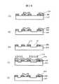
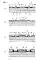
掘り込みタイプの位相シフトマスクは次のように作成される。図2A(a)に示すようにマスク基体(石英基板)201の平坦表面上に遮光体となるCr膜202をスパッタ法で被着し、その上にEBレジスト203を塗布する。その上で遮光体用パターンをEB描画(204の矢印で示す)する。現像を行なってレジストパターン205を形成し(図2A(b))、ドライエッチングあるいはウエットエッチングによってCr膜202のエッチングを行ない(図2A(c))、レジストを除去して遮光体パターン206を形成する(図2A(d))。その後EBレジスト207を塗布して位相シフタを形成するためのパターンを露光(208の矢印で示す)する(図2A(e))。現像を行なってレジストパターン209を形成し(図2B(f))、石英基板をドライエッチングによって所望の深さ掘り込む(図2B(g))。レジストを剥離して両開口部210、211の位相差を検査し(図2B(h))、位相差を生じせしめる掘り込み量が目標値に達していない場合再度EBレジスト212を塗布し、シフタパターン描画213を行ない(図2B(i))、現像を行なってシフタパターン214を形成し(図2B(j))、石英基板を再度ドライエッチングし(図2C(k))、レジスト剥離と位相差検査(図2C(l))を行なう。その後、図2C(m)に示すようにウエットエッチングを行なってCr膜を庇にした庇構造215を形成し、掘り込み型位相シフトマスクを製造する。
【0010】
一方、透明膜形成タイプ(以下、シフタ上置きタイプと呼ぶ)の位相シフトマスクは次のように作成される。図3A(a)に示すようにマスク基体(石英基板)301の平坦な表面上に遮光体となるCr膜302をスパッタ法で被着し、その上にEBレジスト303を塗布する。その上で遮光体用パターンをEB描画(304)する。現像を行ないレジストパターン305を形成し(図3A(b))、ドライエッチングあるいはウエットエッチングによってCr膜をエッチングし(図3A(c))、レジストを除去して遮光体パターン306を形成する(図3A(d))。その後、塗布ガラスSOG(Spin on Glass)を塗布し、熱処理等を行なって透明シフタ膜307を形成する(図3A(e))。その後、EBレジスト308を塗布して位相シフタを形成するためのパターンを露光(309)する(図3B(f))。現像を行なってレジストパターン310を形成し(図3B(g))、透明シフタ膜をドライエッチングあるいはウエットエッチングする(図3B(h))。レジストを剥離して両開口部311、312の位相差を検査し、位相シフトマスクを得る。
【0011】
上記した両方法とも遮光体としては金属のCr膜が使用され、しかもその遮光体パターンの正確性が要求されることからこの金属Cr膜は石英基板の平坦な表面上にスパッタ法で形成される。
【0012】
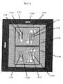
また、この位相シフトマスクの活用形態としては図4に示すように、光学的に孤立パターンと見なせる遮光パターン401に対し、その遮光体401の両側で光学的光路差402により位相差を持たせるシフタ エッジ タイプと、図5に示すようにライン アンド スペースのような近接密集した遮光パターン501に対して開口部に交互に位相シフタ502を配置するレベンソンタイプとがある。ここで図4および図5の403、503はともにガラス基板を示す。どちらの場合も開口部の両側でそこを透過する露光光の位相を反転させる構造において差はない。
【0013】
前述した掘り込み型位相シフトマスクの転写特性上の問題点は、図6(a)に示すようにガラス基板601を掘り込んでいない、あるいは掘り込み量の少ない開口部602(この部分のことを以下0相と呼ぶ)とガラス基板を深く掘り込んだ開口部603(この部分のことを以下π相と呼ぶ)での透過光量がCr遮光体側壁604の下に形成されたガラス基板側面部605での光散乱によって変わり、このことが原因となって0/π差と呼ばれるパターンの寸法差が生じることである。
【0014】
このことを防止するために、図6(b)に示すようにガラス側面部611をCr遮光体613のエッジ612から後退させ、ガラス側面部から散乱される光をCr遮光体で遮るサイドエッチ掘り込み型が提案される。
【0015】
しかし、この場合にはCr遮光体613を支えているガラスの幅614がパターンの微細化にともない細くなり、強度の観点から微細化に耐えられないという問題がある。特に、図6(c)に示すような0相602においてもガラス基板601を掘っている両側掘りタイプのマスクでは、このCrとガラスの接触面積の問題は大きな問題である。細いガラス支柱616でCrの遮光体613を支える必要があり、多数の複雑な微細パターンになればなるほど深刻な問題となる。
【0016】
さらに近年、露光装置のマスク倍率が10×から5×、さらには4×へと移行しており、これに伴ってマスク上の寸法もデバイス寸法の微細化よりさらに加速されて微細化を進ませる必要があるため、この支柱の細さは転写限界を決める決定的課題となってくる。また、製造上このポケット部615に異物がたまり、マスクの歩留まりが上がりにくいという問題がある。また、ドライエッチングを用いてシフタを掘り込む際には、エッチング マイクロ ローディング効果によってパターン寸法にともない掘り込み深さが異なり、したがってパターン寸法に応じて位相角が異なるという問題がある。さらに、図2A〜図2Cに示したようにマスク製造工程数が多く、マスク製造コストが高く、製造にかかる時間が時間が長くTAT(Turn Around Time)が大きく、工程数が多いことから歩留まりが低いという問題がある。
【0017】
また一方、前述したシフタ上置き型位相シフトマスクでは図5に示すように、シフタ502を遮光体であるCr遮光膜501上に形成することから一定の膜厚で位相シフタを形成できず、位相角がパターン寸法に応じて変わり、また一つのパターンの中でもパターン中央部504と周辺部505で位相(即ち、シフタ膜厚)が変わるという問題がある。
【0018】
更に又、上記問題を解決するために位相シフタを先に作成しその上にCr遮光膜を形成しようとしても、シフタからなる段差をもった基板上にスパッタCr膜を無欠陥、高品質に形成するのは極めて困難である。さらに遮光体であるCr膜がシフタ上に形成されるため、Cr膜の表面はフラットではなくなり、傾斜乃至凹凸構造を持ち、露光光の反射が大きくなって、パターン転写特性が劣化するという問題がある。例えば、図16に示すように石英透明基板からなるブランクス1401上に形成されたCr膜1403の表面には反射防止のため酸化Cr層1404を形成し、薄膜干渉現象を使ってCr膜表面からの反射を防止する対策を施こすことが提案されるが、シフタパターン1402にCr膜が一部被るためそのCr膜表面が傾斜乃至凹凸面を呈し、部分的に斜めの部分1405が生じ、そこの酸化Cr膜の膜厚を所定の反射防止条件に正確に制御できないため、同図中に1406及び1407の矢印で示すように反射率が部分的に異なり、転写特性が劣化するという微細パターン化の上で極めて重要な問題がある。
【0019】
従って、前記したような複雑な微細パターンを有する電子装置をかかるマスクと投影露光技術を駆使して精度よく高い歩留まりで製造することはますます難しくなってきている。
【0020】
本発明は、位相シフトマスクを用いた電子装置の改良された製造方法を提供することを目的とするものである。例えば、0.1μm以下の幅や間隔を有する複数の微細パターンで構成される電子装置を投影露光技術及び位相シフトマスク技術を用いて歩留まりよく製造する方法を提供することを目的としている。
【0021】
本発明の他の目的は、かかる電子装置の製造方法に適した微細パターンの形成方法及びそのための改良されたマスクを提供することにある。
【0022】
また、本発明の更に他の目的は、位相シフトマスクを用いた電子装置の製造方法において、露光装置のパターン転写精度を向上させることのできる改良された技術を提供することにある。
【0023】
更に具体的には、位相角制御性の高い位相シフトマスクを用いて投影露光する際に遮光体面からの反射光等の影響による寸法精度劣化の生じない微細パターン形成方法を提供すること及びそれを用いて微細な電子装置を提供することを目的としている。
【0024】
【課題を解決するための手段】
本願において開示される発明のうち、代表的なものの概要を簡単に説明すれば以下の通りである。
【0025】
即ち、本発明では、透明板の平坦な表面に所定の厚さの位相シフタ膜が部分的に形成され、このシフタ膜の端部を覆って非金属からなる所定パターンの遮光膜が部分的に設けられたマスクを用いて、投影露光技術によってこの遮光パターンを被加工物の表面に設けられた感光性膜に転写し、この感光性膜を現像することによって電子装置が製造される。更に具体的には、上記非金属の遮光膜が上記シフタ膜の端部を含んでシフタ膜及び透明板の表面上に部分的に延在して設けられたマスクを用いた投影露光によって上記パターンが転写される。
【0026】
他の本発明では、透明板の平坦な表面に所定の深さ又は高さの凹部又は凸部が部分的に形成され、この凹部又は凸部の端部を覆って非金属からなる所定パターンの遮光膜が部分的に設けられたマスクを用いて、投影露光技術によってこの遮光パターンを被加工物の表面に設けられた感光性膜に転写し、この感光性膜を現像することによって電子装置が製造される。更に具体的には、上記非金属の遮光膜が上記透明板の凹部又は凸部の端部を含んでそれに隣接する透明板の凹部及び凸部表面上に部分的に延在して設けられたマスクを用いた投影露光によって上記パターンが転写される。
【0027】
上記いずれの発明においても、平坦な透明板表面に位相シフト手段が形成されるため転写する際の露光光に対する位相シフタの位相シフト量を所定の領域にわたって精度よく確保することができる。
【0028】
また、上記いずれの発明においても、非金属からなる遮光膜としては転写時の露光光に対して反射率がCr膜等の金属膜よりも小さいものが望ましく、例えば、誘電体、高抵抗体又は有機体の膜を用いることが望ましい。更に具体的には、この遮光膜自身が感光性を呈した膜であれば上記マスク自体を製造するのにも好都合であり、例えば、ノボラック樹脂若しくはフェノール樹脂等のフォトレジスト膜を用いることが望ましい。或いは、ポニアニリン樹脂膜のような感光性膜を用いることが望ましい。
【0029】
誘電体、高抵抗体又は有機体の膜を遮光膜として用いることにより、屈折率の関係から転写時の露光光に対する反射率をCr等の金属膜に比べ小さくすることができるので遮光膜が凹凸表面を有していてもフレア(flare)を小さくすることができ、解像度向上及び寸法精度向上に有益である。また、後述するように転写時の露光光によって遮光膜(即ち、マスクパターン)自体の膜厚に起因してその側壁面に発生する導波管効果(waveguide effect)を小さくできるので、この遮光膜が凹凸表面を有していても遮光膜の膜厚の差に伴う加工寸法差を小さくすることができ加工精度の向上に極めて有益である。
【0030】
このように本発明によれば、マスクにおける位相シフト量を高精度に制御しかつ転写時における解像度乃至寸法精度の向上を図ることができるので、複雑な微細パターンを有する半導体集積回路装置等の電子装置の製造歩留まりを向上させることができる。
【0031】
図1(a)に本発明に係わるマスクの一例を示す。同図より判るように、それは透明石英板等のブランクス1の平坦な表面上にパターニングされた透明の位相シフタ膜2を先に形成した後、位相シフタ膜2の端部でその表面とブランクス1の表面とで構成される段部を覆うように誘電体若しくは高抵抗体、有機体からなる遮光体パターン3が形成された下置き位相シフタ上置き遮光体マスク構造となっている。マスク製造工程を考えると図1(a)のように遮光体パターン面が上側に描かれた方が理解しやすいが、転写時に露光装置にマスクを挿入するときには、図1(b)のような方向で、即ち、感光性ホトレジスト膜12が表面に設けられた半導体基板等の電子装置を構成する被加工物11の表面にこのマスクのパターン面が対向するようにして露光装置に装着され、上方向から即ち、透明ブランクスの裏面から投影露光光15が照射され、被加工物11表面の感光性膜12がこの遮光体3で構成されるマスクパターンで露光される。そして、この露光された感光性膜12を現像処理することによって上記遮光体パターンがそこに転写される。
【0032】
さらに位相シフタ2とマスク基体(いわゆるブランクスガラス)1との間に、転写時の露光光の波長λに対する屈折率n'がブランクスガラスの屈折率よりも大きく位相シフタの屈折率n以下の透明膜(図1では省略)をその膜厚d'として、およそ
sin(2πn'(d'+λ/2(n-1))/λ)=sin(2πn'd'/λ)
の式を満足するように設ければさらに転写精度が向上する。
【0033】
また、位相シフタ2の端部の厚さ方向の断面が傾斜形状(即ち、テーパ形状)であるとその上に形成される遮光体パターンの寸法精度が向上すると共に接着強度が向上するが、その分占有面積を大きくすることになるのでこのテーパ角は45度以上とした方が望ましい。実際的には約60度程度が望ましい。
【0034】
更に又、感光性SOG(Spin On Glass)を用いて位相シフタ2を形成すればマスク作製工程を大幅に削減でき、TATも向上し更にマスク歩留りも向上する。
【0035】
さらに、位相シフトマスクにおける遮光パターン3をフォトレジスト膜によって形成した場合には、実際にフォトマスクを半導体集積回路装置の製造工程に用いるときや実際の位相シフトマスクの製造において以下のように種々の課題があること並びにその解決手段を本発明者等は見出した。
【0036】
まず第1に、位相シフトマスクのシフタパターンと遮光体パターンの相対的な位置決めをするいわゆるシフタと遮光体との間の位置合わせマーク(アライメントマーク)やパターン測定マークのパターン検出が困難である。このことは特に位相シフタを先に形成して作る場合に問題となる。シフタ層はガラス基板を掘り込んだものあるいはSOG等を被着したものであり、ともにその材質がガラス基板と同じあるいはほぼ同じ系統のものである。このためEB描画のアライメント時に用いる電子線に対し、シフタ層のマークのエッジ部の反射率の差が小さく、パターン検出が困難になる。したがってシフタパターンが先に形成されている場合、シフタパターンと遮光体パターンの位置合わせを行なうことが困難である。その解決手段は次の通りである。
【0037】
シフタ層形成に先だって、マスク基板上表面の内転写すべきパターン領域の外側に、すなわち半導体集積回路装置の製造においては集積回路パターン形成領域外に、メタルからなるメタル領域を配置し、そのメタルにシフタパターンや遮光体パターンの描画の際の位置合わせ基準となるアライメントマークを形成する。本手段によって第1の問題は解決される。
【0038】
第2に、製品判定マーク等のような各種情報検出等に用いる所定のパターンの検出が困難となる。例えば、マスク欠陥検査装置においてはマスクのアライメントにハロゲンランプ等が主に用いられるが、マスクを欠陥検査装置に装着する場合に、マスク上の検出マークがレジスト膜パターンによって形成されていると、レジスト膜では光透過率が高く、高いコントランストを得ることができないので、パターンの検出が困難である。このため、マスクと欠陥検査装置とのアライメントが困難になり、良好な検査ができなくなる問題がある。またマスク欠陥検査装置に限らず、例えば露光装置に装着するときもマスクの品種の同定を行なうためのマークが必要となる。この時機械で判読するマークの他に作業者が目視で判読できるマークも載せておくことが作業効率上望ましい。このときガラス基板上に直接シフタやレジスト遮光体で書かれた文字の場合には非常に判読しづらく、判読ミスが起こる。その解決手段は次の通りである。
【0039】
転写すべきパターン領域の外側に、すなわち半導体集積回路装置の製造方法においては集積回路パターン形成領域外に、メタルからなるメタル領域をマスク基体上に配置し、そのメタルあるいはそのメタル上に欠陥検査装置の合わせを行なう基準マークやマスクを同定するための文字や記号等のマークパターンを形成する。このとき、メタルに開口を形成し、基準マークや同定記号とすることも出来るし、メタルプレートを形成し、その上にシフタやレジストでパターンを形成しそのパターンを基準マークや同定パターンとすることも出来る。本手段によって第2の問題は解決される。
【0040】
第3に、マスクを欠陥検査装置や露光装置等に装着する際に異物が発生することによる問題である。上記技術においては、マスクを欠陥検査装置や露光装置等に装着する際や搬送する際に、マスクのレジスト膜が欠陥検査装置や露光装置等のマスク固定部材(例えば真空固定機構)に直接接触することになるので、レジスト膜が欠けたり削れたりすることで異物が発生する。この異物が、例えば検査装置や露光装置のレンズの表面に付着したり、チャンバ内を汚染したり、半導体ウエハの表面に付着することに起因して、パターンの検査精度や転写精度の劣化を招いたり、パターンの短絡不良や開放不良等のような不良が発生したりすることにより、半導体装置の信頼性および製造歩留りが低下するという課題がある。
【0041】
この問題を解決するため、本発明者等は、光学マスクを検査装置や露光装置等のような所定の装置に装着する際や搬送の際に、光学マスクのマスク基板上のレジスト膜からなる遮光パターンと所定の装置の装着部とを接触させないように、遮光パターンをマスク基板の中央部主面上に配置した光学マスクを用いることを提案した。また、本発明者等は、光学マスクを所定の装置に装着する際に、光学マスクのマスク基板の主面においてレジスト膜からなる遮光パターンが存在しない領域(即ち、周辺部)に所定の装置の装着部を接触させた状態で所定の処理を行うことを提案した。これらの手段によって第3の問題は解決される。
【0042】
【発明の実施の形態】
本願発明を詳細に説明する前に、本願における用語の意味を説明すると次の通りである。1.デバイス面とは、半導体ウエハの主面であってその面にフォトリソグラフィにより、複数の半導体チップ領域に対応するデバイスパターンが形成される面を言う。2.半導体集積回路ウエハ(半導体集積回路基板)または半導体ウエハ(半導体基板)とは、半導体集積回路の製造に用いるシリコン単結晶基板(一般にほぼ平面円形状)、サファイア基板、ガラス基板その他の絶縁、反絶縁または半導体基板等並びにそれらの複合的基板を言う。3.有機SOG(Spin On Glass)膜とは、一般にシロキサン重合体または他のモノマーとの共重合体に各種の有機官能基が結合した高分子樹脂を溶剤に溶いて、基板上にスピン塗布して形成された絶縁膜のことである。一般に、無機SOGに比べて、キュア後にクラックが入りにくいため厚めに膜を形成できる特徴がある。またこの有機膜はCVD(Chemical Vapor Deposition)技術によって形成される場合があるので、その場合には単に有機シロキサン系絶縁膜と称する。4.エッチングストッパと言うときは、原則としてエッチング対象膜の当該エッチングストッパ膜に対するエッチング選択比が4以上のものを言う(即ち、AのBに対するエッチング選択比がXとは、AのエッチングレートがXで、Bのエッチングレートが1であることを言う)。なお、エッチングストッパ膜には、塗布ストッパ膜等も含まれる。5.マスキング層は、一般にレジスト膜を言うが、無機マスクや非感光性の有機物マスク等も含むものとする。6.「遮光領域」、「遮光膜」、「遮光パターン」と言うときは、その領域に照射される露光光のうち40%未満(狭義には、30%未満)の光を透過させる光学特性を有する場合を意味している。一方、「透明」、「透明膜」と言うときは、その領域に照射される露光光のうち60%以上(狭義には、90%以上)の光を透過させる光学特性を有する場合を意味している。7.「フォトレジストパターン」とは、感光性の有機膜をフォトリソグラフィの手法により、パターニングされた膜パターンを言う。なお、このパターンには当該部分に関して全く開口のない単なるレジスト膜を含む。8.マスクのパターン面を次の領域に分類される。転写されるべき集積回路パターンが配置される領域:「集積回路パターン形成領域」、ペリクルに覆われている領域:「ペリクルカバー領域」、集積回路パターン形成領域以外のペリクルカバー領域:「集積回路パターン周辺領域」、ペリクルに覆われていない外部領域:「周辺領域」、周辺領域のうち、光学的パターンが形成されている内側の領域:「周辺内部領域」、その他の周辺領域で真空吸着等に使用される領域:「周辺外部領域」。9.半導体の分野では紫外線は以下のように分類される。波長が400nm程度未満で、50nm程度以上を紫外線、300nm以上を近紫外線、300nm未満で200nm以上を遠紫外線、200nm未満を真空紫外線。なお、本願の主な実施例は200nm未満の真空紫外線領域を中心に説明したが、実施の形態2で示すような変更を行えば、250nm未満で200nm以上のKrFエキシマレーザによる遠紫外域でも適用可能であることは言うまでもない。また、100nm未満で50nm以上の紫外線の短波長端領域でも本発明の原理を適用することは同様に可能である。10.マスク遮光材料に関して「メタル」と言うときは、クロム、酸化クロム、その他の金属の同様な化合物を指し、広くは金属元素を含む単体、化合物、複合体等で遮光作用のあるものを含む。11. 「レベンソン型位相シフトマスク」とは、遮光領域で隔てられた隣り合う開口の位相を相互に反転させて、その干渉作用によって鮮明な像を得ようとする位相シフトマスクの一種である。
【0043】
以下の種々の実施例においては便宜上その必要があるときは、複数のセクションまたは実施の形態に分割して説明するが、特に明示した場合を除き、それらはお互いに無関係なものではなく、一方は他方の一部または全部の変形例、詳細、補足説明等の関係にある。また、以下の種々の実施例において、要素の数等(個数、数値、量、範囲等を含む)に言及する場合、特に明示した場合および原理的に明らかに特定の数に限定される場合等を除き、その特定の数に限定されるものではなく、特定の数以上でも以下でも良い。さらに、以下の種々の実施例において、その構成要素(要素ステップ等も含む)は、特に明示した場合および原理的に明らかに必須であると考えられる場合等を除き、必ずしも必須のものではないことは言うまでもない。同様に、以下の種々の実施例において、構成要素等の形状、位置関係等に言及するときは、特に明示した場合および原理的に明らかにそうでないと考えられる場合等を除き、実質的にその形状等に近似または類似するもの等を含むものとする。このことは、上記数値および範囲についても同様である。
【0044】
また、本願において半導体集積回路装置というときは、シリコンウエハやサファイア基板等の半導体または絶縁体基板上に作られるものだけでなく、特に、そうでない旨明示された場合を除き、TFT(Thin-Film-Transistor)およびSTN(Super-Twisted-Nematic)液晶等のようなガラス等の他の絶縁基板上に作られるもの等も含むものとする。
【0045】
以下、本発明の種々の実施例を図面に基づいて詳細に説明する。
【0046】
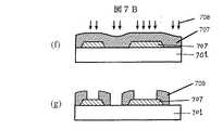
(実施例1) 図7A(a)から(e)及び図7B(f)から(g)は、本発明の一実施例による位相シフトマスクの製造方法を示すための工程別の要部断面図である。
【0047】
まず図7A(a)に示すように石英ガラス基体(ブランクス)701の平坦な主表面上に位相シフタ膜702を形成した。その膜厚dは、露光光の波長をl、シフタ膜702の露光波長に対する屈折率をnとしたときにλ/{2(n−1)}となるように設定した。ここでシフタ膜702はスパッタ技術で形成したSiOxとしたがこれに限るものではない。露光光を透過し、膜厚及び屈折率が均質な膜であれば他の膜も用いることが出来る。特にSnOxやTiOx等の屈折率が高い膜は膜厚dを薄くすることができ、その後のレジスト遮光体パターン形成が容易になることから好ましい。屈折率が1.6以上でその膜厚効果が現れてくる。また導電性膜であれば次に示すレジスト膜をEB描画する際に電荷のチャージアップの影響を受けることがないため、このシフタ膜自体又は少なくともその表面或いは裏面が導電性を呈していることが好ましい。シフタ膜の表面或いは裏面に設ける導電膜としてはITO膜等がよい。また、耐久性を向上させるためにシフタ膜701を被着した後で加熱処理を施したが、膜厚dの設定はこの熱処理後の膜厚である。ここでは熱処理として200℃、30分のベークを行なったがこれに限るものではない。
【0048】
また、このシフタ膜の厚さは位相角を決定する重要なものなので熱処理を含めた膜形成後測定し、基準値以内に収まっていない場合は除去し再形成した。この膜厚ばらつきの許容値は寸法及び必要寸法精度によって左右されるが1%程度である。平坦な主表面上にシフタ層702を被着することから膜厚均一性がとりやすく、またエッチング時のマイクロ ローディング効果による寸法毎に位相角(膜厚)が変わるという問題も生じないことから高い解像度と寸法精度を容易に得ることが出来た。ここではシフタ膜形成法としてスパッタを用いたが、CVDや塗布形成法も用いることが出来る。特に塗布形成法は膜厚の均一性が良いという特長があり、この場合は0.2%の均一性で膜形成することも可能であった。これは位相角ズレに換算して約0.1度に相当する精度の高いものである。また位相シフタ膜の膜欠陥(ピンホール欠陥や異物欠陥)を検査し、欠陥が検出された場合はシフタ膜を再生、再作成した。初期の段階で位相欠陥につながる欠陥対策が可能となるため工程管理が容易となる。
【0049】
次に、図7A(b)に示すようにシフタ層702の上にEBレジスト膜703を塗布形成し、所望のシフタ描画パターンでEB描画(704)した。シフタ層702が導電性を呈していない場合にはこのレジスト膜703の上に水溶性導電膜を形成し、EB描画時の電荷のチャージアップ対策を施した。このような対策を施さないとチャージアップにより描画パターンの位置ずれを起こす。本実施例では導電膜を形成しておいたためチャージアップによる描画位置ずれは起きなかった。チャージアップを防止するために必要な導電率を調べたところシート抵抗で50MΩ/cm2以下の抵抗に抑えれば十分な効果があることがわかった。
【0050】
次に、図7A(c)に示すように現像を行なってレジストパターン705を形成し、その後図7A(d)に示すようにこのレジストパターン705をマスクにしてエッチングによってシフタ膜702を加工した。
【0051】
次いで、図7A(e)に示すようにレジスト705を除去してシフタパターン706を石英ガラス基体701の平坦な主表面上に形成した。この際、シフタパターン706の端部の側面をテーパ加工しておいた。テーパー角θは約60度とした。ここでエッジ検出法を用いて位相シフタパターン706における欠け欠陥や残り欠陥を検査した。この工程では遮光体がこのシフタパターン706の回りを取り囲んでいないためにエッジ検出法でシフタ欠陥を検査出来るので、簡便でかつ検出精度の高い位相欠陥検査を行なうことができた。
【0052】
その後、図7B(f)に示すようにEBレジスト膜707を塗布し、所望の遮光体パターンをEB描画(708)した。この露光の際もシフタパターン706の描画の際と同様チャージアップ防止のための導電膜形成が有効である。本実施例においてはシート抵抗30MΩ/cm2の導電膜(図示省略)をレジスト膜707上に被着した。この後に下地をエッチングする必要がないため、このEBレジスト膜707のエッチング耐性は気にする必要はなく、その分シフタ膜エッジでの段差(又は凹凸)に対して被覆性に優れ、かつこのような段差を有する基板上で寸法精度の出るレジスト材料を選択するとこのマスクの寸法精度を高めることが出来る。段差上で寸法精度を出すためには裾引き形状ではなく断面形状がほぼ垂直に加工できるレジスト材を用いるとよい。実際、本実施例ではほぼ90度の垂直な断面形状を有するレジストを用いた。またこのEBレジストは転写時の露光光に対して遮光体の役目も担うため、露光光を強く吸収する材料とする必要がある。
【0053】
このEBレジスト膜707を構成する材料と前記した図7A(b)の工程で用いた位相シフタパターン形成用のEBレジスト膜703とは同じレジスト材を使用することも可能ではあるが、少なくともEBレジスト膜707の方はそれが現像されて転写時の遮光パターンとして使用されるので前述したようにエッチング耐性は不問で、その端部がシャープに、ほぼ垂直に、加工されやすい性質をもったもので転写時の露光光に対して遮光性をもったものを使用することが必要である。つまり、それぞれの使用される目的に応じてEBレジスト703と707とは違った材料のものを用いるのがベターである。
【0054】
本発明者等の種々の試作実験結果から、本実施例ではこのEBレジスト707としてはノボラック樹脂を主体とするフォトレジスト材を用いた。特に、このノボラック樹脂は図8に照射光の波長に対する光吸収特性測定結果を示すように波長193nmのArF露光光に対する光吸収が強いため、ArFエキシマレーザで転写露光する際に十分な遮光体として機能することが判った。また、ノボラック樹脂に限らずフェノール樹脂などベンゼン環を有する樹脂は、KrF(248μm)露光光等に対しては光吸収度は小さいが、ArF露光光に対しては光吸収度が顕著に大きく、従ってArF用の遮光体としては好適である。なお、これらのノボラック樹脂やフェノール樹脂自体は有機体であるとともに誘電体乃至高抵抗体でもある。
【0055】
また、このようにベンゼン環を含んだEBレジストでは波長100nmから200nmにかけて光を強く吸収する性質があるため、転写時の露光波長としては100nmから200nmが好適である。レジストの吸光度としては、消衰係数(複素屈折率の虚部)で表して0.5以上、出来れば1.0以上が後述の膜厚とOD値との関係から望ましかった。なお本実施例では消衰係数1.0の材料を用いた。この遮光膜の厚さは薄すぎると遮光性能が不十分となり、厚すぎるとレジストパターン側壁の効果によって開口部の透過率が開口寸法によって変わるという問題が生じる。段差エッジ部付近に生じるレジスト膜厚の薄くなるところで露光光に対する透過率をOD値で表現して3以上に下げると十分な遮光体として機能する。OD値を4以上とすると遮光部を僅かに透過してくる光の位相の影響も問題なくなり、OD値を5以上とすると透過光の影響は全くなくなった。なおOD値とは、入射光をIin、透過光をIoutとしたとき、log10(Iout/Iin)で表される値のことである。開口部エッジ部分のレジスト膜厚d'の上限としては最小開口幅wの3倍以下、即ち3w以下、とすることが転写パターン精度上望ましかった。またその膜厚の下限は、露光光の波長をλ、位相シフタの露光光に対する屈折率をnとするとき、λ/{2(n−1)}であった。これ以下の膜厚では遮光性が不足した。実際の転写結果から実用的には0.2μm以上を確保することが好ましかった。
【0056】
なお、前記したようにシフタ膜706のエッジ部をテーパ加工してあるためレジストの被覆性が良く、膜厚変動も比較的少ないためレジストパターン寸法精度が高かった。直接段差上を横切るパターンはないが、レジスト膜厚変動の影響は広い範囲に及ぶためこのテーパ加工の効果は大きい。ここではテーパ角θを60度としたが、これより値を小さくしてよりなだらかにすると膜厚変動が減る。一方で位置合わせ余裕を持たせたうえでそのテーパ部を覆うように遮光体であるレジストパターンを形成しておく必要があることから、最小の遮光体パターン幅が制限される。最適なテーパ角は、パターン最小ルール及びシフタとこのレジストパターンとの位置合わせ精度の見合いから決まる。種々の実験結果から45度以上のテーパ角とすればよいことが確認できた。
【0057】
その後、図7B(g)に示すように現像を行なって遮光体レジストパターン709を形成した。さらに加熱あるいはDUV(deep UV)光を照射あるいはその双方の処理を行った。この処理を施すことによりレジスト遮光体709の転写時における露光光に対する照射耐性が高まった。
【0058】
本実施例による位相シフトマスクは位相誤差0.5度以内という極めて位相制御性が高いものであり、その寸法依存性もないことから、パターン転写を行なったときの寸法精度及び解像度が高かった。またレジスト遮光体709はブランクス701及び位相シフタ706と大きな面積で接触しておりパターン剥がれ等の欠陥も発生しなかった。さらに製造工程も少ないためマスク製造歩留まりも高く、またTATも短かった。さらに遮光体709の表面での露光光の反射率は大気側で6%、ブランクス側で1%となり、図16で説明した酸化Crを表面に被着して反射防止処理を行ったCrの反射率を大きく下回ることができ、この反射光がもとで起こるレンズ内フレアによる転写解像性能低下を防止することが出来た。なお、反射防止処理を行ったCrの反射率は大気側で13%であった。この差はさらに基板段差にともない生じる傾斜部分で大きくなった。
【0059】
なお、本実施例ではブランクス701の平坦な表面上に形成したシフタ層702を加工することにより位相が互いに180度反転する0相とπ相を形成したが、このシフタパターンに加え、ブランクスを一部エッチングして位相差を調整することも有効である。このとき露光光の波長をλ、ブランクスの露光波長に対する屈折率をn0、シフタ層の露光波長に対する屈折率をn1、及びシフタ層の膜厚をd1とすると、ブランクスをλ/{2(n0−1)}−(n1−1)d1/(n0−1)の深さだけエッチングすると位相反転条件となり、そのマスクを用いて転写すると最も高い解像度が得られた。この方法はシフタ形成後に位相を調整することができるのでマスク製造の歩留まりを更に向上させるのに効果があった。
【0060】
(実施例2) マスクの製造工程を示す図9A(a)から(e)及び図9B(f)から(g)を用いて本発明の第2の実施例を説明する。
【0061】
まず、図9A(a)に示すように石英ガラス基体(ブランクス)801の平坦な主表面上に干渉制御層802を形成し、その後その干渉制御層802上にシフタ膜803を形成した。干渉制御層802は露光光を透過する透明膜で、その膜の露光光に対する屈折率n'は石英ガラス基体の屈折率より大きくシフタ膜803の屈折率nと同じかそれよりも小さいものである。その干渉制御層802の膜厚d'は露光光の波長をλとすると、sin(2πn’(d’+λ/2(n-1))/λ)=sin(2πn’d’/λ)を満足することが望ましい。この条件にするとブランクス801とシフタ層803との間で生じる露光光の多重干渉が0相とπ相で差がなくなり、寸法精度が向上するためである。シフタ層803と同じ材料を用いることもできるが、より望ましくはシフタ層803の加工の時にエッチングストッパとなるようなエッチング選択比を有し、かつ屈折率がほぼ等しいものが最適である。さらに導電性も持つと次に示すレジストEB描画の際に電荷のチャージアップの影響を受けることがないため好適である。ここでは干渉制御層802としてTiOxを、シフタ層803としてもTiOxを用いたが、例えば干渉制御層802としてSnOxを、シフタ層803としてTiOxのように違う材料を用い、加工精度を高めるのも効果があった。
【0062】
シフタ層803の膜厚dは、露光光の波長をλ、シフタ膜803の露光波長に対する屈折率をnとしたときにλ/{2(n−1)}となるように設定した。シフタ層803にTiOxという屈折率の高い膜を用いたため膜厚dを薄くでき、その後のレジスト遮光体パターン形成が容易になった。また耐久性を向上させるために干渉制御層802およびシフタ膜803を被着した後で加熱処理を施したが、膜厚dの設定はこの熱処理後の膜厚である。ここでは熱処理として200℃、30分のベークを行なったがこれに限るものではない。また、シフタ層803の膜厚は位相角を決定する重要なものなので熱処理を含めた膜形成後測定し、基準値以内に収まっていない場合は除去及び再形成した。この膜厚ばらつきの許容値は寸法及び必要寸法精度によって左右されるが1%程度である。前記実施例1と同様に、透明板の平坦表面上にシフタ層803を被着することから膜厚均一性がとれやすく、またエッチング時のマイクロ ローディング効果による寸法毎に位相角(膜厚)が変わるという問題も生じないことから高い解像度と寸法精度を容易に得ることが出来た。ここではシフタ膜803の形成法としてスパッタを用いたが、CVD技術や塗布形成法も用いることが出来る。
【0063】
次に、図9A(b)に示すようにシフタ層803の上にEBレジスト膜804を塗布形成し、所望のシフタ描画パターンでEB描画(805)した。シフタ層803が導電性でない場合はこのレジスト804の上に水溶性導電膜を形成し、EB描画時のチャージアップ対策を施した。このような対策を施さないとチャージアップにより描画パターンの位置ずれを起こす。本実施例では導電膜を形成しておいたためチャージアップによる描画位置ずれは起こらなかった。
【0064】
次に、図9A(c)に示すように現像を行なってレジストパターン806を形成し、その後図9A(d)に示すようにこのレジストパターン806をマスクにしてエッチングによってシフタ膜803を加工した。前記したように干渉制御層802としてSnOxを、シフタ層803としてTiOxを用いた場合には、例えばCF系ガスを使用してエッチングすることにより干渉制御層802がエッチング進行のストッパーとして働き、シフタ膜803を精度良く加工できると共にブランクス801の表面がエッチングされたり加工歪み等の影響が生じないことことが判った。
【0065】
さらに、図9A(e)に示すようにレジスト806を除去してシフタパターン807を干渉制御層802上に形成した。ここでエッジ検出法で位相シフタ欠け欠陥や残り欠陥を検査した。遮光体がこのシフタパターンの回りを取り囲んでいないためエッジ検出法でシフタ欠陥を検査出来るため簡便でかつ検出精度の高い位相欠陥検査を行なうことが出来た。
【0066】
その後、図9B(f)に示すようにEBレジスト膜808を塗布し、所望の遮光パターンでもってEB描画(809)した。この露光の際もシフタパターンの描画の際と同様チャージアップ防止のための導電膜形成が有効である。本実施例においてはシート抵抗40MΩ/cm2の導電膜(図示せず)をレジスト膜808上に被着した。
【0067】
この後に下地をエッチングする必要がないため、このEBレジスト808のエッチング耐性は要求されない。その分段差被覆性に優れ、段差基板上で寸法精度の出るレジストを選択するとこのマスクの寸法精度を高めることが出来る。段差上で寸法精度を出すためには断面形状が垂直で、裾引き形状でないレジストを用いるとよい。またこのEBレジスト808は転写時の露光光の遮光体の役目も担うため、転写時の露光光を強く吸収する材料とする必要がある。本実施例ではノボラック樹脂に波長が248nmの光に対する吸光剤を混合したレジスト(これ自体は誘電体、高抵抗体でもあり、また有機体でもある)を用いた。吸光剤の影響で転写時の波長248nmのKrF露光光に対する十分な遮光体として機能した。一般に強い吸光剤を添加するとレジストの解像性能が極端に低下するが、このレジストはEBレジストであり、添加する吸光剤は波長248nmに対するものであることからマスク作製には十分な解像度を得ることができた。レジストの吸光度としては、消衰係数で表して0.5以上、出来れば1.0以上が後述の膜厚とOD値との関係から望ましかった。なお本実施例では消衰係数0.6の材料を用いた。膜厚は薄すぎると遮光性能が不十分となり、厚すぎるとレジストパターン側壁の効果によって開口部の透過率が開口寸法によって変わるという問題が生じる。段差エッジ部付近に生じるレジスト膜厚の薄くなるところで露光光に対する透過率をOD値で表現して3以上に下げると十分な遮光体として機能する。OD値を4以上とすると遮光部を僅かに透過してくる光の位相の影響も問題なくなり、OD値を5以上とすると透過光の影響は全くなくなった。シフタ層807として屈折率の高いTiOxを用いたためシフタパターンによる段差が少なく、被覆するレジストのカバレージも向上するため、このような吸光剤を添加したレジストでも十分な解像性能を得ることができた。
【0068】
その後、図9B(g)に示すように現像を行なって遮光体レジストパターン810を形成した。さらに加熱あるいはDUV照射あるいはその双方の処理を行った。この処理を施すことによりレジスト遮光体810の転写時の露光光に対する照射耐性が高まった。
【0069】
本実施例による位相シフトマスクは位相誤差0.5度以内という極めて位相制御性が高いものであり、その寸法依存性もないことから、KrF露光光でパターン転写を行なったときの寸法精度及び解像度が高かった。ブランクスより屈折率の高いシフタ層を用いたが、シフタ層とブランクスの間で生じる多重干渉の悪影響もなく互いに位相が180度反転した0相とπ相間の寸法ばらつきもなかった。またレジスト遮光体810は干渉制御層802及び位相シフタ807と大きな面積で接触しておりパターン剥がれ等の欠陥も発生しなかった。特に干渉制御層802として導入したTiOxではそれらの間の密着性が良かった。さらに位相シフトマスクの製造工程も実施例1と同様に少ないため製造歩留まりも高く、またTATも短かった。さらに遮光体810の表面での露光光の反射率は大気側で6%、ブランクス側で1%となり、酸化Crを表面に被着して反射防止処理を行ったCrの反射率(大気側で15%)を大きく下回ることができ、この反射光がもとで起こるレンズ内フレアによる転写解像性能低下を防止することが出来た。なお、シフタ706のエッジ部の断面をテーパ上に形成しておけば実施例1と同様に効果的である。
【0070】
(実施例3) マスクの製造工程を示す図10(a)から(e)を用いて本発明の第3の実施例を説明する。
【0071】
まず、図10(a) に示すように石英ガラス基体(ブランクス)901の平坦な主表面上に感光性シフタ膜902を形成した。この感光性シフタの材料としては有機SOGに酸発生剤を添加したものを用いた。酸発生剤としてはTPS(トリフェニルスルフォニウムトリフレート)を用いたがこれに限るものではない。感光性シフタも有機SOGに限るものではなく、露光光に対し透明で照射耐性があり、かつマスク描画の際に感光性を有するものであればよい。ここで用いた感光性シフタ膜902の露光光(波長193nm)に対する屈折率は1.58と石英ガラスの屈折率1.56と大きな差がなかったため直接ブランクス901の平坦な主表面上に感光性シフタ902を形成したが、屈折率に差がある場合は実施例2と同様に干渉制御膜を形成するとシフタ層内に生じる多重干渉を低減できて寸法精度上効果がある。またブランクス901上に導電膜を形成しておくことも実施例2と同様に、続く感光性シフタ膜の描画の際にチャージアップ防止効果があった。ここでは塗布により感光性シフタ膜902を形成したが、光CVD法など他の方法を用いてもよい。但し、塗布形成法は簡便で欠陥発生も少ないという特長がある。他の塗布形成膜としてはメチルシラザンに酸発生剤を添加したものなどがある。シフタ膜を塗布した後120℃の熱処理を行なった。膜形成後欠陥検査を行ないピンホール欠陥や異物欠陥がないことを確認した。これらの欠陥がある場合はシフタ膜を除去し、再形成した。
【0072】
シフタ層902の膜厚dは後で述べるデンシファイベークの後にλ/{2(n−1)}となるように補正を加えた値にした。ここで、露光光の波長をλ,デンシファイベークの後のシフタ膜902の露光波長に対する屈折率をnとした。
【0073】
次に図10(b)に示すように感光性シフタ層902を所定のパターンで直接EB描画(903)した。感光性シフタ層902の上には水溶性導電膜を形成し(図示なし)、EB描画時の電荷のチャージアップ対策を施した。このような対策を施さないとチャージアップにより描画パターンの位置ずれを起こす。本実施例では導電膜を形成しておいたためチャージアップによる描画位置ずれは起きなかった。
【0074】
次に、図10(c)に示すように現像を行なってシフタパターン904を形成した。その後、露光光照射耐性向上及び風化防止のためにシフタパターン904を加熱処理した。ここでは熱処理として250℃、30分のベークを行なったがこれに限るものではない。高温にするほど耐性が向上する。また、シフタ層904の膜厚は位相角を決定する重要なものなので熱処理後測定し、基準値以内に収まっていない場合は除去及び再形成した。この膜厚ばらつきの許容値は寸法及び必要寸法精度によって左右されるが1%程度である。平坦表面上にシフタ層を被着することから膜厚均一性がとれやすく、またエッチング時のマイクロ ローディング効果による寸法毎に位相角(膜厚)が変わるという問題も生じないことから高い解像度と寸法精度を容易に得ることが出来た。
【0075】
その後エッジ検出法で位相シフタ欠け欠陥や残り欠陥を検査した。遮光体がこのシフタパターンの回りを取り囲んでいないためエッジ検出法でシフタ欠陥を検査でき、簡便でかつ検出精度の高い位相欠陥検査を行なうことが出来た。このようにして無欠陥で位相制御性の優れた位相シフタパターンをエッチング工程なしに塗布、ベーク、露光及び現像工程のみで形成することができた。
【0076】
その後、図10(d)に示すようにレジスト905を塗布し、所望の遮光パターンでもってEB描画(906)した。この露光の際もシフタパターン904の描画の際と同様チャージアップ防止のための導電膜形成が有効である。本実施例においてはシート抵抗40MΩ/cm2の導電膜(図示せず)をレジスト膜905上に被着した。この後に下地をエッチングする必要がないため、このEBレジスト膜905のエッチング耐性の厳密性は必要でなく、その分段差被覆性に優れ、段差基板上で寸法精度の出るレジスト材を選択するとこのマスクの寸法精度を高めることが出来る。
【0077】
このEBレジスト膜905は転写時の露光光の遮光体の役目も担うため、転写時の露光光を強く吸収する材料とする必要がある。本実施例ではフェノール樹脂を主体とするフォトレジストを用いたがこの材料は露光光(波長193nm)に対する消衰係数が0.9でありArF露光光を用いる転写時に十分な遮光体として機能した。レジストの吸光度としては、消衰係数で表して0.5以上、出来れば1.0以上が後述の膜厚とOD値との関係から望ましかった。膜厚は薄すぎると遮光性能が不十分となり、厚すぎるとレジストパターン側壁の効果(導波管効果)によって開口部の透過率が開口寸法によって変わるという問題が生じる。段差エッジ部付近に生じるレジスト膜厚の薄くなるところで露光光に対する透過率をOD値で表現して3以上に下げると十分な遮光体として機能する。OD値を4以上とすると遮光部を僅かに透過してくる光の位相の影響も問題なくなり、OD値を5以上とすると透過光の影響は全くなくなった。
【0078】
なお、本実施例ではEBレジストを用いたがKrFやi線等の光露光用レジストとし、描画にレーザなどを用いることも出来る。レーザ描画はEB描画に比べれば解像度は若干落ちるものの、電荷のチャージアップの問題が無くなり、露光時の発生熱の影響も少なくなるという特長がある。
【0079】
その後、図10(e)に示すように現像を行なって遮光体フォトレジストパターン907を形成した。さらに加熱あるいはDUV照射あるいはその双方の処理を行った。この処理を施すことによりレジスト遮光体907の転写時の露光光に対する照射耐性が高まった。
【0080】
本実施例による位相シフトマスクは位相誤差0.5度以内という極めて位相制御性が高いものであり、その寸法依存性もないことから、ArF露光光でパターン転写を行なったときの寸法精度及び解像度が高かった。
【0081】
レジスト遮光体907は位相シフタ904や基板901と大きな面積で接触しておりパターン剥がれ等の欠陥も発生しなかった。マスクの製造工程数は前記実施例に比べ大幅に少なく、しかも欠陥発生の少ない塗布、ベーク、露光、現像、検査工程のみからなっているためマスク製造の歩留まりも高く、またTATも短かった。
【0082】
さらに遮光体表面での露光光の反射率は大気側で6%、ブランクス側で1%と酸化Crを表面に被着して反射防止処理を行ったCrの反射率(大気側で18%)を大きく下回ることができ、この反射光がもとで起こるレンズ内フレアによる転写解像性能低下を防止することができた。この差はさらに基板段差にともない生じる斜めの部分で大きくなった。
【0083】
(実施例4) マスクの製造工程を示す図11A(a)から(e)及び図11B(f)から(j)を用いて本発明の第4の実施例を説明する。
【0084】
まず、図11A(a)に示すようにブランクス1001上にレジスト膜1002を通常の方法で塗布し、所望のシフタパターンをEB描画し(1003)、現像を行なって図11A(b)に示すようにレジストパターン1004を形成した。
【0085】
その後、図11A(c)に示すように透明板(ブランクス)1001の露出した表面を所定の深さに部分的にエッチして凹部即ち、溝又は窪みを形成した。
【0086】
次に、図11A(d)に示すようにレジスト膜1004を通常の方法で除去し、ブランクス1001の主表面に凹部及び又は凸部で構成される段差を露出せしめた。この段差、すなわち図中の凸部1005と凹部1006との間の段差を段差計あるいはAFM(Atomic Force Microscope)で計測し位相差に換算、あるいは干渉計測によって位相差を直接測定した。その露光波長に対する位相差が180度に対し、所望の範囲に収まっておれば図11B(i)に示す工程へ進む。ここではその範囲を±1.5度とした。その値は必要寸法精度にリンクして変わり、高い寸法精度が必要なほどその範囲は狭くなる。所望の範囲外の時は以下の工程へ進む。
【0087】
本実施例では位相差が165度であったため、図11A(e)に示すように再度レジスト膜1007を塗布し、シフタパターン露光(1008)を行ない、現像を行なって図11B(f)のようにレジストパターン1009を形成した。
【0088】
その後、図11B(g)に示すようにブランクス1001を再度エッチングした。レジスト膜1009を除去して図11B(h)に示すように位相シフトパターン1010及び1011を持つブランクスを形成した。
【0089】
同図中の二つの表面1010及び1011の露光光に対する位相差を測定し、位相差が180度に対し所望の範囲に収まっていることを確認した。その後エッジ検出モードで位相欠陥検査を行なった。欠陥は検出されなかったので次の工程に進んだが、欠陥が検出された場合はFIB方法等を用いて欠陥修正を行うか、欠陥修正が困難なときは再作製を行なう。この方法では比較的初期の工程で位相欠陥検査がしかもエッジ検出法という検査精度の高い方法で行えるという特長がある。その後洗浄を行なった。
【0090】
次に図11B(i)に示すようにEBレジスト膜1012を塗布し、遮光すべき部分を形成するためのパターン露光(1013)を行なった。その後現像を行なって図11B(j)に示すようにこのレジストからなる遮光体パターン1014を形成した。
【0091】
なお、述べてこなかったが実施例1から3と同様、EBレジスト膜の上には水溶性導電膜を形成し、EB描画時の電荷のチャージアップ対策を施した。チャージアップ防止法としてはこの他にITO等の導電性膜をレジストの下側に形成しておく方法も有効である。導電膜が残る場合はSEM等を使っての寸法測定の際、チャージアップの影響を受けないため高精度なQCが行なえて有効である。
【0092】
またレジスト膜1014は転写時の露光光の遮光体の役目も担うため、転写時の露光光を強く吸収する材料とする必要がある。本実施例ではノボラック樹脂を主体とするフォトレジストを用いた。ノボラック樹脂は波長193nmのArF露光光に対する光吸収が強いためArF露光光での転写時に十分な遮光体として機能した。この他の材料としてはポリアニリン樹脂などがある。ポリアニリン樹脂はそれ自体に導電性があるためEB描画時にチャージアップしにくく、この意味でも有効である。ポリアニリン樹脂を用いた場合は上述の水溶性導電膜の塗布を省くことができた。
【0093】
本実施例ではCr被着とCrエッチングがない分マスクの製造工程数が少なく、また高品位なCr被着が不要な分製造コストを下げることが出来た。さらに遮光体表面での露光光の反射率は大気側で6%、ブランクス側で1%と酸化Crを表面に被着して反射防止処理を行ったCrの反射率を大きく下回ることができ、この反射光がもとで起こるレンズ内フレアによる転写解像性能低下を防止することができた。
【0094】
なお、本実施例ではブランクス基板のπ相側のみをエッチングすることにより0相とπ相との間に180度の位相差を持たせたが、この他にπ相に加え0相もエッチングする両掘りとし、両者の間に180度の位相差を持たせてもよい。
【0095】
(実施例5) 前述した実施例1から4においては、シフタ膜であろうとブランクスの凹凸であろうと、いずれもこれらのシフタパターンの位置を基に正確に位置決めを行なって遮光体パターンを描画する必要がある。しかしながらシフタパターンはブランクスと材料系が近寄っている又は同じであるので、シフタパターン特にそれらの段差部(境界部、凹凸部)をEBで観察して位置決めを行なうと位置決め精度が低下する。そこで第3の層を金属膜で形成し、そこに合わせ用マークを予め形成しておき、そのマークを検出してシフタパターン描画やレジスト遮光体パターン描画を行なった。実施例3に則して、その工程図を図12(a)から(e)をもとに実施例5として説明する。
【0096】
まず、図12(a)に示すようにブランクス1101の平坦表面上にEB描画の際の合わせ基準マーク1103が形成されたメタル層1102を形成した。なおこのメタル層領域はパターン転写フィールドの外側に形成した。ブランクスの中央部分には誘電体、高抵抗体又は有機体の膜(例えば、フォトレジスト膜)を配置し、その外側にメタル層を配置した。ここではメタルとしてCrを用いたが、その他W、Ti、Mo、MoSi、Ta、又はWNx等を用いることも出来る。加工が容易でブランクス上でEBの反射コントラストが取れる材料が望ましい。
【0097】
次に、図12(b)に示すようにその上に感光性シフタ層1104及び水溶性導電膜1105を形成し、シフタパターンのEB露光、現像を行なって図12(c)に示すようにシフタパターン1106を形成した。このシフタパターン1106を露光する際、基準マーク1103をEBで検出し、その位置を参照して描画を行なった。位置合わせマークがメタルパターンで出来ているため精度良く検出することが出来た。
【0098】
その後、図12(d)に示すようにEBレジスト1107を塗布し、その上に水溶性導電膜1108を形成した。
【0099】
その後、遮光体パターンをEB露光し、図12(e)に示すようにレジストパターン1109を形成した。この遮光体パターンをEB露光する際、基準マーク1103をEBで検出し、その位置を参照してEB描画を行なった。マークがメタルパターンで出来ているため精度良く検出することが出来た。シフタパターン1106とレジスト遮光体パターン1109の相対的位置合わせはメタルマーク1103を介して行なった、いわゆる3層間合わせになるが、合わせ基準マーク検出コントラストが高いため、50nmの合わせ精度が得られた。一方、シフタパターンを合わせ基準マークに用いてレジスト遮光体パターンを描画したときはマーク検出の際の信号コントラストが十分取れず、合わせ精度は200nmになり、さらにマークの誤検出を起こし、描画ができない場合があった。
【0100】
本工程は実施例3の場合について示したが、他の実施例でも同様にメタル基準マークを用いて合わせ描画を行なった。その結果、十分な合わせ精度を得ることができた。なお、シフタ層が十分な導電性をもつ場合はメタル基準マークでなく、シフタパターンマークを用いても必要な位置合わせ精度を得ることが出来た。
【0101】
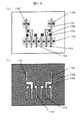
図13(a)は製造されたマスクを上面から見たときの概要を示す。パターン転写フィールド領域1110の外側にメタルからなる外枠1101が形成されており、その外枠領域の中にシフタパターンおよびレジスト遮光体パターン合わせ基準マーク1111、及びマスクの置かれた位置を露光装置側に認識させ、アライメントを行なうためのレチクルマーク1103が形成されている。さらに外枠上のメタル層にレチクル(マスク)を識別するための識別マーク1112を形成した。
【0102】
レチクルマーク1103がメタルで形成されていると、ほとんどの波長の光でその位置をモニタしても高い精度でマーク検出を行なうことが出来る。レチクルマーク1103は、遮光体外枠1101の金属膜の一部が除去され、その下層の透明なマスク基板が露出されることによって形成されている。したがって、マスクの位置検出に通常のハロゲンランプ等を用いているような露光装置を用いた場合においても、レチクルマーク1103を透過した光のコントラストが充分にとれるので、レチクルマーク認識能力を向上させることができる。このため、マスクと露光装置との相対的な位置合わせを容易に、しかも高い精度で行うことが可能となる。本発明者等の検討結果によれば、通常のフォトマスクと同等の精度で位置合わせが可能となった。
【0103】
このことを露光装置の構成を参照しながら説明する。図17は種々の実施例で用いた縮小投影露光装置の一例を示したものであり、縮小投影露光装置の光源1501から発する露光光はフライアイレンズ1502、照明形状調整アパーチャ1503、コンデンサレンズ1504,1505およびミラー1506を介してマスク1507を照射する。このマスク1507は、遮光パターンが形成された主面(第1の主面)を下方(半導体ウエハ1509側)に向けた状態で載置されている。したがって、上記露光光は、マスク1507の裏面(第2の主面)側から照射される。
【0104】
これにより、マスク1507上に描かれたマスクパターンは、投影レンズ1508を介して試料基板である半導体ウエハ1509上に投影される。マスク1507の第1の主面には、異物付着によるパターン転写不良を防止するためのペリクル1510が必要に応じて設けられている。
【0105】
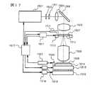
なお、マスク1507はマスク位置制御手段1511で制御されたマスクステージ1512上に真空吸着され、位置検出手段1513により位置合わせされ、その中心と投影レンズの光軸との位置合わせが正確になされている。半導体ウエハ1509は,試料台1514上に真空吸着されている。試料台1514は、投影レンズ1508の光軸方向、すなわちZ軸方向に移動可能なZステージ1515上に載置され、さらにXYステージ1516上に搭載されている。Zステージ1515およびXYステージ1516は、主制御系1517からの制御命令に応じてそれぞれの駆動手段1518、1519によって駆動されるので、所望の露光位置に移動可能である。その位置はZステージ1515に固定されたミラー1520の位置として、レーザ測長器1521で正確にモニタされている。
【0106】
さらに、位置検出手段1513には、例えばハロゲンランプが用いられている。すなわち、特別な光源を位置検出手段1513に用いる必要がなく(新しい技術や難しい技術を新たに導入する必要性がなく)、通常の縮小投影露光装置を用いることができる。
【0107】
一方、レジスト遮光体でレチクルマークを形成するとレチクルアライメントを行なうことが困難となる。これは遮光率の関係から一般に露光光より長い光を十分なコントラストで遮光することが出来ないためである。
【0108】
露光装置のステージや搬送装置に接触する部分にはレジスト膜等の遮光膜や感光性シフタ層、あるいは塗布形成シフタ膜を残さず、製造工程の途中でその部分の膜を除去しておいた。なお、残さざるを得ない時はCr等の金属膜でその表面を露出しないように被覆しておいてもよい。このことにより搬送によって生じる異物の発生を防止することができた。このような処置を施さない場合には異物が発生し、転写欠陥を引き起こすことがある。
【0109】
図13(b)はマスクを上面から見たときの別の例を示す。パターン転写フィールド領域1202の外側にシフタパターンおよびレジスト遮光体パターン合わせ基準マーク1201、及びレチクル(マスク)を識別するための識別マーク領域1203が形成されている。合わせ基準マーク1201、及び識別マーク領域1203はメタルで形成されている。合わせ基準マークは描画歪みを補正する目的から少なくともマスク四隅には配置されていることが望ましい。
【0110】
すなわち、四隅の位置をモニタし、歪み補正を行ないながら描画する。マスク識別マーク1204はメタル領域1203上にレジストで描かれる。ブランクス上のレジストマークでは肉眼での識別が困難であったが、メタル上ではレジストが薄膜であるためレジスト膜内で光干渉を起こし、反射率が変わって識別が可能となった。ただしこの識別マークは露光装置等のステージや搬送機構に接触しない場所に形成しておく必要がある。有機の脆い膜のため接触すると異物の発生源となるためであり、本発明に係わるマスクを取り扱う際には極めて重要である。
【0111】
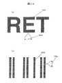
上記例ではメタル上にレジストで識別マークを形成する例を示したが、ここではブランクス(石英ガラス)上に直接識別マークを設ける方法を図14(a)及び(b)をもとに説明する。
【0112】
図14(a)は図13(b)でのメタル領域1203上にフォトレジストで描かれた「RET」という文字2201によるマスク識別マークであり、図14(b)は文字ではなく所謂バーコード2203で描かれたマスク識別マークであり、いずれも複数のスリット状のフォトレジスト膜が0.5μm乃至2.0μmピッチの間隔(2202、2204)をもって並列配置され或いは一つのフォトレジスト膜に上記ピッチで多数のスリットが刻まれて形成されている。実際には1.0μmのピッチで描かれたが、一種の回折格子効果により反射率が増大し識別することができる。特に、(b)のように表示しておくとコード体系の設定の仕方を任意に決めることができるので製造上の木目細かい管理情報に利用でき、また製造上の種々の情報の漏洩乃至秘密保持にも有効である。
【0113】
(実施例6) 本実施例6においては、マスクのパターン形成面(第1の主面)に異物が付着しないように作用する透明薄膜ペリクルをマスクの主面上に配置した例を説明する。これ以外は、前記実施例1から5と同様である。なお、ここでは、例えば前記実施例5で説明したマスクと同じようにマスク基板の外周部に金属膜からなる遮光パターンを設けたマスクを用いて説明する。
【0114】
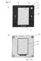
本実施例6のマスクの具体例を図15に示す。なお、図15(a)はマスク1301の平面図を、(b)はマスク1301を所定の装置に装着した時の様子を示した要部断面図を(c)はその応用例の要部断面図をそれぞれ示している。
【0115】
本実施例6においては、マスク1301の主面(第1の主面)側に、ペリクル1302がペリクル貼り付けフレーム1303を介して接合されて固定されている。ペリクル1302は、マスク1301のパターン形成主表面に異物が付着することを避けるために、マスク基板の主面あるいは主面および裏面から一定の距離までに設けた透明な保護膜を持つ構成体である。この一定の距離は、保護膜表面上の付着異物と異物の半導体ウエハ等の被加工物体表面への転写性を考慮して設計されている。
【0116】
ペリクル1302は、マスク1301のペリクルカバー領域に配置されている。すなわち、ペリクル1302は、マスク1301の集積回路パターン形成領域の全体1304および上記周辺内部領域に形成されたメタル遮光パターン1305の一部を覆うように平面的に配置されている。
【0117】
本実施例においては、ペリクル張り付けフレーム1303の基部が、マスク1301の前記周辺内部領域におけるメタル遮光パターン1305に直接接触した状態で接合固定されている。これにより、ペリクル張り付けフレーム1303の剥離を防止できる。一方、ペリクル張り付けフレーム1303の取り付け位置にレジスト膜が形成されていると、ペリクル1302の取り付けや取り外しの際に、このレジスト膜が剥離し異物発生の原因となる。本実施例においては、ペリクル張り付けフレーム1303を遮光パターン1305に直接接触させた状態で接合するので、そのような異物発生を防止できる。このような効果は、ペリクル張り付けフレーム1303をマスク基板1301に直接接触させた状態で接合固定しても得られる。
【0118】
また、前記実施例5と同様に、図15(b)に示すように、マスク1301と投影露光装置の真空吸引装着部1306とが接触する部分にはレジスト膜等の有機膜が存在しないようにした。同図ではメタル膜1305が存在している。これにより、前記実施例5と同様にレジスト膜の剥離や削れ等による異物の発生を防止できる。
【0119】
また、本実施例においては、メタル遮光パターン1305内に位置校正用のマークパターン1307が形成されている。この位置校正用のマークパターン1307は、電子線描画装置を用いてマスク上に所定のパターンを描画する際に、マスク自体から直接マスクの位置情報を検出するためのパターンである。すなわち、本実施例においては、マスク基板の集積回路パターン形成領域に、所定の集積回路パターンを電子線描画装置を用いてパターン形成する際に、そのマスク基板におけるマークパターン1307を何秒かに1回の割合で読みとることにより、パターン描画工程中にパターンを描画するための電子線の照射位置を補正(調整)しながらパターン描画を行うようにされている。これにより、電子線描画装置によるパターン描画位置精度をさらに向上させることが可能である。このようなマークパターン1307を設けたのは、例えば次の理由からである。
【0120】
通常の電子線描画装置においてはマスクへの描画処理は減圧された真空中で行う。真空中におけるマスクの保持は、電子線描画装置の移動ステージ上のマスク保持部の3点ピンにマスク基板またはマスク基板の装着されたカセットを押し付け、押し付けピンで機械的に固定している。ここで、通常の電子線描画装置においては、描画中の電子線の位置ドリフトによるパターン描画位置ずれを防止する目的で、マスク保持部に取り付けられた位置検出用のマークパターンを描画中に複数回検出して位置ずれを補正している。
【0121】
マスク保持部(ステージ)のマスク基板は上述のように機械的に固定されているのでマスク保持部のマークパターンとマスク基板との相対的な位置関係は一定となっているはずであるが、実際には高速で移動するステージの衝撃により、マークパターンとマスク基板との間にわずかな位置ずれが生じる場合がある。このため、電子線描画工程中にマスク基板の位置をマークパターンから読みとっているにもかかわらず、描画パターンに位置ずれが生じてしまう。
【0122】
そこで、本実施例においては、マスク(マスク基板)自体に位置補正用のマークパターン1307を配置し、マスク基板自体からその位置を直接検出するようにした。これにより、上記マスク基板の保持のずれも含めて補正することができるので、パターンの配列誤差を低減することができる。このようなマークパターン1307は、例えば当該パターン位置が光透過領域になっているか、遮光領域になっているかによって構成され、そこに照射された位置検出ビームまたは検出光の反射状態によって情報の検出がなされるようになっている。位置検出手段は、電子線描画装置の電子線を使用するもの、レーザライタによるレーザ光を使用するものまたは他の方式を用いることができる。特に位置精度の高い装置の適用が望ましい。なお、図15中の1308は回路パターンを、1309は露光装置にマスクの位置を示すレチクルマークを示している。
【0123】
また、図15(c)では、マスク基板1301上の金属膜1305に接着剤等を介して取り付けられたペリクル1302の枠1303の側壁面に、内蔵されているマスクの識別マーク「RETICLE−A」が描かれている。このようにすることによってペリクルの上部表面の面積を前述した種々の検査、測定や観察のために有効に活用することができる。なお、この例においても前述したようにペリクルはフォトレジスト膜が設けられていないマスク基板表面上に取り付けられている。
【0124】
このような実施例6によれば、前記種々の実施例で得られる効果の他に次の効果を得ることができる。(1)マスクにペリクルを設けたことにより、マスクに異物が付着するのを防止し、その異物付着に起因する転写パターンの劣化を抑制または防止できる。(2)ペリクル張り付けフレームを遮光パターンまたはマスク基板に直接接触させた状態で接合したことにより、ペリクルの取り付けや取り外しに際して、遮光パターン形成用のレジスト膜が剥離したり削れたりするのを防止できる。このため、そのレジスト膜の剥離や削れ等に起因する異物の発生を防止できる。(3)マスク自体に電子線描画装置での電子線の描画位置補正用のマークパターンを設けたことにより、電子線描画装置でのパターン描画位置精度を向上させることが可能となる。
【0125】
(実施例7) 第7の実施例をマスクパターンの平面図である図18を用いて説明する。
【0126】
図18の1601はレジスト遮光体面、1602は0相の開口部、1603及び1604はπ相の開口部である。1602および1603はパターン転写が可能な寸法を持つ本体パターンであり、1604はその像が直接は転写されず近傍にあるパターンの解像性能を向上させるためのいわゆる補助パターンである。ここでは本体パターン1603及び1604の最小寸法は0.2μm(ウエハ上での寸法であり、レンズの縮小率が4×なのでマスク上での寸法は0.8μm)以下とし、図示はしていないがウエハ上で0.1μmから0.2μmまで各寸法のパターンを入れた。補助パターン1604の線幅はウエハ上で0.04μm(マスク上は0.32μm)とした。
【0127】
このマスクは実施例1にしたがって作製したが、露光波長にともなうレジスト遮光体の材料選択の問題を除いて他の実施例にしたがって作製したものでも構わない。本マスクをレンズの開口数NAが0.6のArFエキシマレーザスキャナに装着し、ArFネガレジストに転写した。
【0128】
その結果、レジスト遮光体1601は十分な遮光効果を示し、フィールド領域にレジストが残ることはなかった。またレベンソン位相シフトにより本体パターン1602及び1603を5%という高い寸法精度で形成することができた。また、これらの補助パターンに挟まれた本体パターンの解像度はCrを用いた従来の位相シフトマスクを用いた場合よりも高かった。それは、遮光体がレジストという高抵抗体、誘電体であるためガイドウエーブ効果(即ち、導波管効果)が小さく、さらに反射の少ない材料を使用したためである。また、レベンソン位相シフト部でも0/π差現象は起こらず、この意味でも高い寸法精度が得られた。但し、この効果は転写寸法にしてパターン幅では0.16μm以下、パターンピッチでは0.32μm以下から現われ、それより大きい寸法では従来法による位相シフトマスクを用いた場合と変わらなかった。レンズの開口率NAを変えて検討を行ったところ、パターンピッチがλ/NA以下であるときには従来法に比べて特に転写精度が高かった。
【0129】
(実施例8) 本発明のマスク及びパターン形成方法を使って半導体集積回路装置を作製した。図19(a)はその代表的なパターンレイアウトを示す平面図である。
【0130】
同図中の1701は不純物拡散層等の半導体領域、1702は半導体領域とのコンタクト、1703、1704、1706、1707はゲート配線、1705は配線層とのビアホール(Via、接続孔)を示す。回路の動作速度を上げ、またパッキングデンシティを向上させるためには、拡散層等の半導体領域の上に形成されているアクティブなゲート配線の寸法が細く、かつその寸法精度が高いこと、およびゲート配線のピッチを決定するゲート配線間隙1708が狭いことが要求される。
【0131】
図19(b)は図19(a)のゲート配線を形成するために用いた位相シフトマスクの平面図である。ここでは実施例1に沿って作製したマスクを用いた。但し、他の実施例に添って作製したマスク、例えば実施例3に沿って形成したマスクも用いることもできる。図中の1709がレジスト遮光体で、レベンソン配置になるようにシフタ層(π相)が開口部に交互に配置されている。このマスクを用い、NAが0.6のArFスキャナを使ってパターン転写を行ったところ、0.1μmという極めて狭いパターン間隙1708を得、しかも1704や1706で示されるπ相における寸法と1703や1707で示される0相における寸法が一致し、いわゆる0/π差のないパターン転写が実現できた。
【0132】
さらにパターンエッジ部が比較的密に配置された1703や1704といった場所と疎な1706や1707の場所での寸法差も小さく、その差はレンズの特性に基づく補正の範囲に収まるものであった。これらは遮光体が高抵抗体、誘電体であることによるウェーブガイド効果(導波管効果)の低減、表面反射の低減に基づくものである。
【0133】
Cr遮光体を有する位相シフトマスクを用いた場合には本実施例のマスクを用いた場合に比べ20%程転写寸法精度が低いことを確認できた。このゲートパターン形成方法により動作周波数が高く、かつパッキングデンシティが高くチップの小さな半導体集積回路装置を作製することができた。チップが小さくなるとウエハ1枚あたりから取得できるチップ数が高まるだけでなくチップの製造歩留まりも向上するため、作製コストを大幅に低減できる。
【0134】
(実施例9) 本実施例のシフタエッジ位相マスクを用いて微細ゲートパターンを形成した。その時用いた位相マスクを図20(a)に、バイナリーマスクを図20(b)に、そして転写して形成したレジストパターンを図20(c)に示す。
【0135】
同図中の1801は形成すべきパターンの輪郭、1802はゲート配線の細線を形成するための線幅の狭いレジスト遮光体パターン部、1803はレジスト遮光体、1804は0相の開口部、1805はπ相のシフタ層が形成された開口部、1806は透明ガラス部、1807は遮光体パターン、1808、1809は転写形成されたゲートパターンである。図20(b)のマスクとしては1808がCrからなるCrバイナリーマスクを用いることもできるが、ここでは1807がレジスト遮光体からなるレジストマスク遮光体バイナリーマスクを用いた。
【0136】
図20(a)の第1のマスクを露光装置に装着してポジレジスト上に露光を行った後、図20(b)の第2のマスクを露光装置に装着して上記レジストに重ね露光を行ない、レジストを通常の熱処理及び現像を行ってレジストパターンを形成した。
【0137】
本実施例ではNAが0.63のArFスキャナを用い、幅60nmの極めて細いゲート配線1808を再現性よく得ることができた。通常のシフタエッジ位相シフトマスクでは細線遮光体部1802で機械的強度の問題が生じるのでマスク良品歩留りが低いが、本実施例のマスクではそのような問題はなくマスク歩留りが高い。
【0138】
さらに、Cr先形成のブランクス掘り込み型シフタエッジ位相シフトマスクでは、前述したように、シフタ部1802のブランクスを掘り込む際側壁反射による解像性能の低下を防止するためサイドエッチを行うが、遮光体細線1802が細いためこのサイドエッチ量を十分に確保することができず転写性能に影響を与え、転写されたレジストパターンの寸法ばらつきは10%程度となるのに対し、本実施例では転写されたレジストパターンの寸法ばらつきは5%と小さくすることができた。
【0139】
(実施例10) 本発明のマスク及びパターン形成方法を使って複数の半導体メモリ素子からなる電子回路装置を1枚の半導体ウエーハに作製した。図21(a)から(d)はこのメモリ素子の製造の主な工程を示す断面図である。
【0140】
図21(a)に示すように、P型のSi半導体71を基板に用い、その表面に素子分離技術を用いてSiO2からなる素子分離領域72を形成する。次に、素子分離領域72が設けられていない半導体表面に厚さ200nm以下のSiO2等のゲート絶縁膜を介して、例えば厚さ150nmの多結晶Siからなるワード線(ゲート電極)73を形成し、さらにその上に化学気相成長法を用いて例えば150nmのSiO2膜を被着し、異方的に加工してワード線73の側壁にSiO2のサイドスペーサ74を形成する。次に、通常の方法でN型拡散層(ソース又はドレイン領域)75を形成する。
【0141】
次に図21(b)に示すように、通常の工程を経て多結晶Siまたは高融点金属金属シリサイド、あるいはこれらの積層膜からなるデータ線76を形成し、その上部をSiO2等の絶縁膜で被覆する。次に図21(c)に示すように、通常の工程を経て半導体領域に接続されて絶縁膜上に延在した多結晶Siからなるキャパシター電極(蓄積電極)78を形成する。その後、Ta2O5、Si3N4、SiO2、BST、PZT、強誘電体、あるいはこれらの複合膜などを被着してキャパシタ用絶縁膜79を形成する。引き続き多結晶Si、高融点金属、高融点金属シリサイド、あるいはAl、Cu等の低抵抗の導体を被着しプレート電極80を形成する。
【0142】
次に図21(d)に示すように、通常の工程を経て配線81を形成する。次に通常の配線形成工程やパッシベーション工程を経て複数のメモリ素子からなる電子回路装置を作製した。
【0143】
なお、ここでは、代表的な製造工程のみを説明したが、これ以外は通常の製造工程を用いた。また、各工程の順番が前後しても本発明は適用できる。上記素子製造工程におけるリソグラフィ工程で本発明を適用可能である。例えば、微細パターンを形成する必要のない工程あるいは高い寸法精度が要求されない工程には本発明は必ずしも適用する必要はない。パッシベーション工程での導通孔形成工程や、パターンが大きなイオン打ち込みマスク形成用のパタン形成工程には本発明は適用しなかった。本発明のパターン形成方法が特に有効な工程は素子分離領域、ワード線、キャパシター電極、及び配線の形成工程である。
【0144】
次に、リソグラフィで形成したパターンについて説明する。図22(a)は製造したメモリ素子を構成する代表的なパターンのメモリ部のパターン配置を示す。82がワード線、83がデータ線、84がアクティブ領域、85がキャパシター電極、86が電極取り出し孔のパターンである。図22(b)は別のメモリ素子を構成する代表的なパターンのメモリ部のパターン配置を示す。87がワード線、88がデータ線、89がアクティブ領域、90が蓄積電極、91が電極取り出し孔のパターンである。ワード線とデータ線のパターン形成に本発明を用いた。また図22(b)においては蓄積電極のパターン形成にも本発明を用いた。ここに示したパターン形成以外でも最小設計ルールを用いる工程では本発明を用いた。
【0145】
本発明を用いて作製した素子の特性は、従来法を用いて作製した素子の特性と比較すると特性が良好であった。具体的にはワード線の線幅バラツキが小さい事から、データの読み出しスピードが速く特性が安定しており、蓄積電極の面積バラツキが小さい事からデータの保持特性が安定している等の特性の改善が実現できた。また、素子の良品取得歩留まりでも改善効果が得られた。
【0146】
(実施例11) 次に、所謂ツインウエル方式のCMIS(Complementary MIS)回路を有する集積回路装置の製造に適用した例を工程毎の要部断面を示した図23(a)から(d)をもとに説明する。
【0147】
図23(a)のように、半導体ウエーハの主要部を構成するN型Siの半導体基板101の上表面部にN型ウエル102及びP型ウエル103が形成され、両ウエルにまたがるようにSiO2からなる素子分離用のフィールド絶縁膜105が選択酸化技術によって形成され、この絶縁膜105によって囲まれた各ウエルの半導体活性領域にはPチャンネル型MISFET(Qp)及びNチャンネル型MISFET(Qn)が形成されている。なお、111、112はソース、ドレイン領域を構成するP型半導体領域であり、113、114ソース、ドレイン領域を構成するN型半導体領域であり、106、107はSiO2等からなるゲート絶縁膜であり、115、116はゲート絶縁膜上に設けられたゲート電極である。これらゲート電極115、116は、例えば低抵抗ポリシリコン膜をCVD法によって堆積した後、その膜をKrFエキシマレーザを使った縮小投影露光装置及び前述した本発明の種々の実施例で作成されたフォトマスクを用いたフォトリソグラフィ技術と通常のエッチング技術とによって形成されている。ゲート電極長は例えば0.2μm程度である。上記111〜114の半導体領域はそれぞれゲート電極に対して自己整合的に形成されている。
【0148】
次に、図23(b)に示すように、SiO2からなる層間絶縁膜118をCVD法等によって堆積した後、その上部にポリシリコン膜を堆積し、それをKrFエキシマレーザを使った縮小投影露光装置及び前述した本発明の種々の実施例で作成されたフォトマスクを用いたフォトリソグラフィ技術と通常のエッチング技術とによってパターニングし、そこに不純物を部分的に導入することにより配線119及び抵抗120が形成される。
【0149】
次に、図23(c)に示すように、SiO2からなるSOG膜122を堆積した後、層間絶縁膜118及びSOG膜122に半導体領域及び配線119の一部が露出する複数の接続孔124がKrFエキシマレーザを使った縮小投影露光装置及び前述した本発明の種々の実施例で作成されたフォトマスクを用いたフォトリソグラフィ技術と通常のエッチング技術とによって形成される。
【0150】
次いで、図23(d)に示すように、アルミニューム(Al)又はAl合金からなる金属膜をスパッタリング技術によって堆積した後、その金属膜をKrFエキシマレーザを使った縮小投影露光装置及び前述した本発明の種々の実施例で作成されたフォトマスクを用いたフォトリソグラフィ技術と通常のエッチング技術とによってパターニングすることによって、第1層配線126から127が形成される。
【0151】
これ以降は、第1層配線の上部に第1層配線の形成と同様な方法で第2層配線や第3層配線(図示せず)が形成され、大規模なロジックタイプの半導体集積回路装置(LSI)が製造される。
【0152】
カスタムLSIでは、その回路システムを設計する際に特に第1層配線を中心にマスクデバッグが行われることが多い。かかるLSIのTATを小さくするためには、この第1層配線に対応するマスクを供給するタイミングや速さが極めて重要であり、また必要となるマスク枚数も多くなるのでこの工程に本発明を適用するのは極めてその効果が大きい。また、第2層配線での最小パターン寸法は0.35μmと露光波長(0.248μm)に比べて十分太いものであったが、そこにも本発明のフォトマスクを適用した。通常のCrマスクよりもコストを低くし、またTATを短くすることができた。
【0153】
以上の説明から理解されるように、本発明はDRAM(Dynamic Random Access Memory)、SRAM(Static Random Access Memory)またはフラッシュメモリ(EEPROM)等のようなメモリ素子を有する半導体集積回路装置、マイクロプロセッサ等のような論理回路を有する半導体集積回路装置あるいは上記メモリ回路と論理回路とを同一半導体基板に設けて構成される混載型の半導体集積回路装置にも適用できる。特に、論理回路を有するロジックやメモリとロジックを混載するシステムLSIでは、ユーザニーズに合わせてパターン設計から製造に至るまでの工間を短くし、すばやくユーザに供給することに付加価値があるため、マスク製作時間の短い本発明は特に有効であった。
【0154】
なお、本発明の技術思想は、半導体集積回路装置の製造方法に適用されることに限定されるものではなく、例えば液晶基板や超電導装置、磁気ヘッド、マイクロマシーン等のような他の電子回路装置等の製造方法にも適用できる。
【0155】
(実施例12) 図24にこの実施例12で用いた1枚のマスクの平面図を示す。図中の2101はメタル遮光体、2102はレジスト遮光体、2103は露光装置用アライメントマーク部である。露光装置としてはスキャナを用いた。実施例4に沿って位相シフトマスクを作製した。転写すべきパターンは2104部と2105部に示されているように同じものが露光装置のスキャン方向に上下に配置されている。但し、そのパターンの位相配置は互いに反転させてある。すなわち、本体パターン2106、2107、2108にはそれぞれπ、0、0相を配置をしたが、対応する2106'、2107'、2108'にはそれぞれ0、π、π相を配置した。また補助パターン2109にはπ相が配置されているが、2109’には0相が配置されている。このマスクをスキャナに装着してスキャン露光した。その際の2104部を1チップと見なし、2105部が2104部と重なって即ち多重露光されるようにチップ送りを行った。このように多重に露光することにより転写パターンの寸法の0/π差は全く生じなくなった。なお、本方法は特にスキャナでその効果を発揮する。これはスキャナではスリット状のレンズの一部を使って露光するからである。これに対し、ステッパのようにレンズの全体を使って露光される方法ではレンズ収差が2104部と2105部とで異なり、収差の足し合わさった像が転写されてしまうため転写精度が低下してしまう。
【0156】
【発明の効果】
本願によって開示される発明のうち、代表的なものによって得られる効果を簡単に説明すれば、次の通りである。(1)微細パターン形成用のマスクパターンを製作するにあたり位相シフトマスクの製造工程数が減り、かつスパッタCr膜の製膜、Cr膜のエッチングのような異物の発生しやすい工程を用いることがないのでマスク製造歩留りも向上する。製造工程数の削減はマスク作製TATの面でも大きな効果がある。(2)位相角の制御精度が向上する。特に実施例1から3に示したブランクス上にシフタ膜を形成する方法でこの効果が大きい。エッチングによるマイクロ ローディング効果がほとんどでないため各種寸法で位相角を揃えることができ、転写パターンの寸法制御性が高い。(3)位相角変化部、すなわちシフタのエッジを誘電体、高抵抗体、又は有機体からなる遮光膜(例えば、フォトレジスト膜)が被覆するため、転写時に遮光膜の側壁からの反射やガイドウェーブ効果を小さくすることができ、細線化によるマスクパターン強度不足の問題もおこらず転写パターンの微細化が容易に行える。表面反射も小さく転写パターンの寸法精度が高い。また、レベンソンタイプの位相シフトの寸法0/π差が小さい。(4)光学マスクのマスク基板の外周にメタル遮光領域を設け、その一部を除去することで光学マスクの情報を検出するためのマークパターンを形成したことにより、光学マスクの情報検出能力を向上させることが可能となる。またマスクを露光装置に装着したときの異物の発生がない。(5)メタルプレート上にマスク識別記号を入れることにより、容易にマスクを識別することが可能となる。(6)上記(1)〜(5)により、本発明の光学マスクを用いて製造された半導体集積回路装置等の電子回路装置の性能、信頼性、開発TATおよび製造歩留まりを向上させることが可能となる。
【図面の簡単な説明】
【図1】 (a)は本発明の代表例を示す位相シフトマスクの断面図であり、(b)はそれを用いた投影露光方法を示す図である。
【図2A】 (a)〜(e)はマスクの製造工程を示す工程別断面図。
【図2B】 (f)〜(j)はマスクの製造工程を示す工程別断面図。
【図2C】 (k)〜(m)はマスクの製造工程を示す工程別断面図。
【図3A】 (a)〜(e)は他のマスクの製造工程を示す工程別断面図。
【図3B】 (f)〜(i)は他のマスクの製造工程を示す工程別断面図。
【図4】 位相シフトマスクの適用例を示すためのマスク要部断面図。
【図5】 位相シフトマスクの他の適用例を示すためのマスク要部断面図。
【図6】 (a)〜(c)は位相シフトマスクでの課題を説明するためのマスクの要部断面図。
【図7A】 (a)〜(e)は本発明の実施例1に係わる位相シフトマスクの製造工程を示す工程別要部断面図。
【図7B】 (f)及び(g)は実施例1に係わる位相シフトマスクの製造工程を示す工程別要部断面図。
【図8】 フォトレジスト材の光吸収特性を示す特性図。
【図9A】 (a)〜(e)は本発明の実施例2に係わる位相シフトマスクの製造工程を示す工程別要部断面図。
【図9B】 (f)及び(g)は実施例2に係わる位相シフトマスクの製造工程を示す工程別要部断面図。
【図10】 (a)〜(e)は本発明の実施例3に係わる位相シフトマスクの製造工程を示す工程別要部断面図。
【図11A】 (a)〜(e)は本発明の実施例4に係わる位相シフトマスクの製造工程を示す工程別要部断面図。
【図11B】 (f)〜(j)は実施例4に係わる位相シフトマスクの製造工程を示す工程別要部断面図。
【図12】 (a)〜(e)は本発明の実施例5に係わる位相シフトマスクの製造工程を示す工程別要部断面図。
【図13】 (a)及び(b)は本発明に係わる位相シフトマスクの要部平面図。
【図14】 (a)及び(b)は本発明に係わる位相シフトマスクに設けられた文字、記号、マーク等のパターンの平面図。
【図15】 (a)は本発明の実施例6に係わる位相シフトマスクの要部平面図であり、(b)はそのマスクが装置に装着された状態を示す要部断面図であり、(c)はマスクの側面図である。
【図16】 位相シフトマスクでの課題を説明するためのマスクの要部断面図。
【図17】 本発明で用いた露光装置の概要を示した装置概念図。
【図18】 本発明の実施例7に係わるマスクパターンレイアウトを示す要部平面図。
【図19】 (a)は本発明の実施例8に係わる電子回路パターンのレイアウトを示す要部平面図であり、(b)はそのための位相シフトマスクの平面図である。
【図20】 (a)は本発明の実施例9に係わる位相シフトマスクの平面図であり、(b)はバイナリーマスクの平面図であり、(c)は転写して形成したパターンの平面図である。
【図21】 (a)〜(d)は本発明の実施例10に係わる半導体メモリ回路装置の製造工程を示す工程別の素子要部断面図である。
【図22】 (a)及び(b)は半導体メモリでの回路レイアウトパターンを説明する要部平面図である。
【図23】 (a)〜(d)は本発明の実施例11に係わる半導体論理回路装置の製造工程を示す工程別の素子要部断面図である。
【図24】 本発明の実施例12に係わる位相シフトマスクの要部平面図である。
【符号の説明】
1、201、301、601、701、801、901、1001、1101、1301、1401…透明板(ブランクス)、2、307、402、502、702、706、803、807、902、904、1106、1402、…位相シフタ膜、3、206、306、401、501、604、709、810、907、1014、1109、1403、…遮光体パターン、802…透明膜(干渉制御層)、1005…透明板表面の凸部、1006…透明板表面の凹部、1302…ペリクル[0001]
BACKGROUND OF THE INVENTION
The present invention relates to a method for manufacturing an electronic device such as a semiconductor device, a superconducting device, a micromachine, or an electronic device, a pattern forming method used therefor, an optical max used therefor, and a method for manufacturing the same. The present invention relates to a technique effective when applied to an exposure technique.
[0002]
[Prior art]
In the manufacture of a semiconductor integrated circuit device, a lithography technique is used as a method for transferring a fine pattern onto a semiconductor wafer. In the lithography technique, a projection exposure apparatus is mainly used, and a photomask pattern mounted on the projection exposure apparatus is transferred onto a semiconductor wafer to form a device pattern.
[0003]
A normal photomask is produced by processing a light shielding material such as chromium (Cr) formed on a flat surface of a transparent quartz substrate. That is, a light shielding film made of chromium or the like is formed in a desired shape on a flat surface of a quartz substrate. For example, after processing an electron beam sensitive resist on the light shielding film, a desired pattern is drawn on the electron beam sensitive resist with an electron beam drawing apparatus, and then a resist pattern having a desired shape is developed by development. Then, dry etching or wet etching is performed using the resist pattern as a mask to process the light shielding film. Thereafter, after removing the resist, washing or the like is performed to form a light-shielding pattern having a desired shape on the transparent quartz substrate.
[0004]
In recent years, with the progress of higher integration of LSIs, there has been a demand for improvement in operation speed and miniaturization of circuit patterns. This tendency is particularly severe in the gate pattern that greatly affects the transistor operation speed. In some logic LSI products, a gate pattern of 0.1 μm is already formed using an exposure apparatus of a KrF excimer laser (wavelength 248 nm).
[0005]
Further, miniaturization of semiconductor memories has been promoted in order to reduce the cost, and a DRAM (Dynamic Random Access Memory) with a half pitch 0.18 μm rule has been commercialized with an exposure apparatus using a KrF excimer laser. . Development of a 0.13 μm rule DRAM using a KrF scanner is also underway.
[0006]
The reason why pattern resolution much smaller than the exposure wavelength is possible is largely due to an exposure method called super-resolution. Among these super-resolutions, what is effective in forming a fine pattern is called a phase shift exposure method, which is disclosed in, for example, Japanese Patent Application Laid-Open No. 58-173744. This phase shift exposure method forms a structure called a phase shifter that alternately inverts the phase of exposure light by sandwiching a light-shielding portion between the exposure light transmission portion of the photomask, that is, the window portion where the glass surface is exposed. This is a method of performing exposure using Since the phase of the light passing through both transmission parts is inverted, there occurs a place where the light amplitude becomes zero at the light shielding part existing between them. If the amplitude is 0, the intensity of light is also 0, and the resolution is dramatically improved.
[0007]
In addition, JP-A-9-211837 and JP-A-5-289307 disclose techniques relating to masks.
[0008]
[Problems to be solved by the invention]
The phase shifter is a digging type that digs a part of the glass plate of the photomask base, a type that forms a transparent film with a film thickness that reverses the phase on the photomask base, and mixes these two There are some types.
[0009]
The digging-type phase shift mask is produced as follows. As shown in FIG. 2A (a), a
[0010]
On the other hand, a phase shift mask of a transparent film forming type (hereinafter referred to as a shifter-mounted type) is produced as follows. As shown in FIG. 3A (a), a
[0011]
In both of the above methods, a metal Cr film is used as the light shielding body, and the accuracy of the light shielding body pattern is required. Therefore, the metal Cr film is formed on the flat surface of the quartz substrate by sputtering. .
[0012]
Further, as a form of utilization of this phase shift mask, as shown in FIG. 4, a shifter that gives a phase difference to the
[0013]
The problem with the transfer characteristics of the digging-type phase shift mask described above is that the glass substrate 601 is not dug as shown in FIG. The glass substrate side surface portion 605 formed below the Cr light shielding side wall 604 is transmitted through an opening 603 (hereinafter referred to as the π phase) deeply dug into the glass substrate. This causes a difference in the size of the pattern called a 0 / π difference.
[0014]
In order to prevent this, as shown in FIG. 6B, the side surface of the glass side 611 is retracted from the edge 612 of the Cr light shielding body 613, and the side etch digging that blocks light scattered from the glass side surface by the Cr light shielding body. A built-in type is proposed.
[0015]
However, in this case, there is a problem that the width 614 of the glass supporting the Cr light-shielding body 613 becomes narrower as the pattern becomes finer, and cannot withstand the fineness from the viewpoint of strength. In particular, in the double-sided digging mask in which the glass substrate 601 is dug even in the zero phase 602 as shown in FIG. 6C, the problem of the contact area between Cr and glass is a big problem. It is necessary to support the Cr light shielding body 613 with the thin glass support 616, and the more complicated fine patterns become, the more serious the problem becomes.
[0016]
Further, in recent years, the mask magnification of the exposure apparatus has shifted from 10 × to 5 ×, and further to 4 ×, and accordingly, the dimensions on the mask are further accelerated than the miniaturization of the device dimensions and the miniaturization is advanced. Since it is necessary, the fineness of this support column becomes a decisive issue that determines the transfer limit. In addition, there is a problem that foreign matter accumulates in the pocket portion 615 in manufacturing, and it is difficult to increase the yield of the mask. Further, when the shifter is dug using dry etching, there is a problem that the dug depth varies with the pattern size due to the etching microloading effect, and therefore the phase angle varies depending on the pattern size. Further, as shown in FIGS. 2A to 2C, the number of mask manufacturing processes is large, the mask manufacturing cost is high, the time required for manufacturing is long, the TAT (Turn Around Time) is large, and the number of processes is large, so the yield is high. There is a problem that it is low.
[0017]
On the other hand, in the above-described shifter-mounted phase shift mask, as shown in FIG. 5, since the
[0018]
Furthermore, in order to solve the above problems, even if a phase shifter is first prepared and a Cr light-shielding film is to be formed thereon, a sputtered Cr film is formed on the substrate having a step made of the shifter without defects and with high quality. It is extremely difficult to do. Furthermore, since the Cr film as a light shielding body is formed on the shifter, the surface of the Cr film is not flat, has a tilted or uneven structure, the reflection of exposure light increases, and the pattern transfer characteristics deteriorate. is there. For example, as shown in FIG. 16, a
[0019]
Accordingly, it has become increasingly difficult to manufacture an electronic device having a complicated fine pattern as described above with high accuracy and high yield using such a mask and projection exposure technology.
[0020]
An object of the present invention is to provide an improved manufacturing method of an electronic device using a phase shift mask. For example, an object of the present invention is to provide a method of manufacturing an electronic device composed of a plurality of fine patterns having a width and interval of 0.1 μm or less with a high yield using a projection exposure technique and a phase shift mask technique.
[0021]
Another object of the present invention is to provide a method for forming a fine pattern suitable for a method for manufacturing such an electronic device and an improved mask therefor.
[0022]
It is still another object of the present invention to provide an improved technique capable of improving the pattern transfer accuracy of an exposure apparatus in an electronic apparatus manufacturing method using a phase shift mask.
[0023]
More specifically, it is possible to provide a fine pattern forming method that does not cause deterioration in dimensional accuracy due to the influence of reflected light or the like from the surface of the light shielding member when performing projection exposure using a phase shift mask having high phase angle controllability, and It is intended to provide a fine electronic device.
[0024]
[Means for Solving the Problems]
Of the inventions disclosed in this application, the outline of typical ones will be briefly described as follows.
[0025]
That is, in the present invention, a phase shifter film having a predetermined thickness is partially formed on a flat surface of a transparent plate, and a light shielding film having a predetermined pattern made of a nonmetal covering the end of the shifter film is partially formed. An electronic device is manufactured by transferring the light-shielding pattern to a photosensitive film provided on the surface of the workpiece by a projection exposure technique using the provided mask, and developing the photosensitive film. More specifically, the pattern is formed by projection exposure using a mask in which the non-metallic light-shielding film partially extends on the surface of the shifter film and the transparent plate including the end of the shifter film. Is transcribed.
[0026]
In another aspect of the present invention, a concave portion or a convex portion having a predetermined depth or height is partially formed on the flat surface of the transparent plate, and a predetermined pattern made of a nonmetal is formed covering the end of the concave portion or the convex portion. By using a mask partially provided with a light shielding film, the light shielding pattern is transferred to a photosensitive film provided on the surface of the workpiece by a projection exposure technique, and the electronic device is developed by developing the photosensitive film. Manufactured. More specifically, the non-metallic light-shielding film is provided so as to partially extend on the concave and convex surfaces of the transparent plate adjacent to and including the concave or convex ends of the transparent plate. The pattern is transferred by projection exposure using a mask.
[0027]
In any of the above inventions, since the phase shift means is formed on the surface of the flat transparent plate, the phase shift amount of the phase shifter with respect to the exposure light at the time of transfer can be ensured accurately over a predetermined region.
[0028]
In any of the above inventions, the light shielding film made of a non-metal preferably has a reflectance lower than that of a metal film such as a Cr film with respect to exposure light at the time of transfer. It is desirable to use an organic film. More specifically, if the light-shielding film itself is a film exhibiting photosensitivity, it is convenient for manufacturing the mask itself. For example, it is desirable to use a photoresist film such as a novolac resin or a phenol resin. . Alternatively, it is desirable to use a photosensitive film such as a ponianiline resin film.
[0029]
By using a dielectric, high-resistance, or organic film as the light-shielding film, the reflectivity for exposure light during transfer can be made smaller than that of a metal film such as Cr because of the refractive index. Even if it has a surface, flare can be reduced, which is beneficial for improving resolution and dimensional accuracy. Further, as will be described later, the waveguide effect generated on the side wall surface due to the film thickness of the light shielding film (that is, the mask pattern) itself can be reduced by the exposure light at the time of transfer. Even if it has an uneven surface, it is possible to reduce the difference in processing dimensions due to the difference in the film thickness of the light shielding film, which is extremely useful for improving the processing accuracy.
[0030]
As described above, according to the present invention, the phase shift amount in the mask can be controlled with high accuracy and the resolution or dimensional accuracy at the time of transfer can be improved, so that an electronic device such as a semiconductor integrated circuit device having a complicated fine pattern can be obtained. The production yield of the device can be improved.
[0031]
FIG. 1A shows an example of a mask according to the present invention. As can be seen from the figure, after the transparent
[0032]
Further, between the
sin (2πn '(d' + λ / 2 (n-1)) / λ) = sin (2πn'd '/ λ)
If it is provided so as to satisfy the expression, the transfer accuracy is further improved.
[0033]
Further, if the cross section in the thickness direction of the end portion of the
[0034]
Furthermore, if the
[0035]
Further, when the light-
[0036]
First of all, it is difficult to detect a pattern of an alignment mark (alignment mark) between the so-called shifter and the light shielding body for relative positioning of the shifter pattern of the phase shift mask and the light shielding body pattern, or a pattern measurement mark. This is a problem particularly when the phase shifter is formed first. The shifter layer is formed by digging a glass substrate or depositing SOG or the like, both of which are of the same or substantially the same system as the glass substrate. For this reason, the difference in the reflectance of the edge portion of the mark of the shifter layer is small with respect to the electron beam used at the time of EB drawing alignment, and pattern detection becomes difficult. Therefore, when the shifter pattern is formed first, it is difficult to align the shifter pattern and the light shielding body pattern. The solution is as follows.
[0037]
Prior to the shifter layer formation, a metal region made of metal is arranged outside the pattern region to be transferred on the surface of the mask substrate, that is, outside the integrated circuit pattern formation region in the manufacture of the semiconductor integrated circuit device. An alignment mark is formed that serves as an alignment reference when drawing a shifter pattern or a light-shielding body pattern. By this means, the first problem is solved.
[0038]
Second, it becomes difficult to detect a predetermined pattern used for various information detection such as a product determination mark. For example, in a mask defect inspection apparatus, a halogen lamp or the like is mainly used for mask alignment. When a mask is mounted on a defect inspection apparatus, if the detection mark on the mask is formed by a resist film pattern, Since the film has a high light transmittance and a high contrast cannot be obtained, it is difficult to detect a pattern. For this reason, there is a problem that alignment between the mask and the defect inspection apparatus becomes difficult, and good inspection cannot be performed. Further, not only the mask defect inspection apparatus but also a mark for identifying the type of mask is required when it is mounted on an exposure apparatus, for example. At this time, in addition to the marks that can be read by the machine, it is desirable in terms of work efficiency to place marks that can be read visually by the operator. At this time, in the case of characters written directly on the glass substrate with a shifter or a resist light-shielding body, it is very difficult to read and misreading occurs. The solution is as follows.
[0039]
A metal region made of metal is disposed on the mask substrate outside the pattern region to be transferred, that is, outside the integrated circuit pattern formation region in the method of manufacturing a semiconductor integrated circuit device, and the defect inspection apparatus is on the metal or the metal. A mark pattern such as a character or a symbol for identifying a reference mark or a mask to be aligned is formed. At this time, an opening can be formed in the metal to be used as a reference mark or an identification symbol, or a metal plate can be formed, and a pattern can be formed thereon with a shifter or a resist, and the pattern can be used as a reference mark or an identification pattern. You can also. By this means, the second problem is solved.
[0040]
Third, there is a problem due to the generation of foreign matter when the mask is mounted on a defect inspection apparatus, an exposure apparatus or the like. In the above technique, when the mask is mounted on a defect inspection apparatus or an exposure apparatus or when it is transported, the resist film of the mask directly contacts a mask fixing member (for example, a vacuum fixing mechanism) of the defect inspection apparatus or the exposure apparatus. Therefore, foreign matters are generated when the resist film is chipped or scraped. For example, this foreign matter adheres to the surface of the lens of the inspection apparatus or exposure apparatus, contaminates the inside of the chamber, or adheres to the surface of the semiconductor wafer. There is a problem that the reliability and the manufacturing yield of the semiconductor device are lowered due to occurrence of defects such as short circuit defects and open defects of patterns.
[0041]
In order to solve this problem, the inventors of the present invention have proposed that the optical mask is shielded from a resist film on the mask substrate of the optical mask when the optical mask is mounted on a predetermined apparatus such as an inspection apparatus or an exposure apparatus or is transported. It has been proposed to use an optical mask in which a light-shielding pattern is arranged on the main surface of the central portion of the mask substrate so that the pattern does not come into contact with the mounting portion of a predetermined apparatus. In addition, when mounting the optical mask on the predetermined apparatus, the present inventors have provided the optical mask on the main surface of the mask substrate in a region where there is no light-shielding pattern made of a resist film (that is, the peripheral portion). It was proposed to perform a predetermined process with the mounting part in contact. The third problem is solved by these means.
[0042]
DETAILED DESCRIPTION OF THE INVENTION
Before describing the present invention in detail, the meaning of terms in the present application will be described as follows. 1. The device surface is a main surface of a semiconductor wafer on which a device pattern corresponding to a plurality of semiconductor chip regions is formed by photolithography. 2. A semiconductor integrated circuit wafer (semiconductor integrated circuit substrate) or a semiconductor wafer (semiconductor substrate) is a silicon single crystal substrate (generally a substantially planar circular shape), a sapphire substrate, a glass substrate, or other insulation or anti-insulation used for manufacturing semiconductor integrated circuits. Or a semiconductor substrate etc. and those composite substrates are said. 3. An organic SOG (Spin On Glass) film is generally formed by dissolving a polymer resin with various organic functional groups bonded to a siloxane polymer or copolymer with other monomers in a solvent and spin-coating it onto the substrate. It is the insulating film made. In general, compared to inorganic SOG, there is a feature that a film can be formed thicker because cracks are less likely to occur after curing. Further, since this organic film may be formed by a CVD (Chemical Vapor Deposition) technique, in this case, it is simply referred to as an organic siloxane insulating film. 4). When the term “etching stopper” is used, it means that the etching selectivity of the film to be etched with respect to the etching stopper film is 4 or more in principle (that is, the etching selectivity of A to B is X means that the etching rate of A is X. , B has an etching rate of 1). Note that the etching stopper film includes a coating stopper film and the like. 5. The masking layer generally refers to a resist film, but includes an inorganic mask, a non-photosensitive organic mask, and the like. 6). “Light shielding region”, “light shielding film”, and “light shielding pattern” have optical characteristics that transmit less than 40% (in a narrow sense, less than 30%) of the exposure light irradiated to the region. Means the case. On the other hand, the terms “transparent” and “transparent film” mean the case where the exposure characteristic has optical characteristics that transmit 60% or more (in a narrow sense, 90% or more) of the exposure light irradiated on the region. ing. 7). “Photoresist pattern” refers to a film pattern obtained by patterning a photosensitive organic film by a photolithography technique. This pattern includes a simple resist film having no opening at all for the portion. 8). The pattern surface of the mask is classified into the following areas. Area where the integrated circuit pattern to be transferred is arranged: “Integrated circuit pattern formation area”, Area covered with pellicle: “Pellicle cover area”, Pellicle cover area other than integrated circuit pattern formation area: “Integrated circuit pattern” "Peripheral area", external area not covered by pellicle: "peripheral area", inner area where optical pattern is formed: "peripheral internal area", vacuum suction etc. in other peripheral areas Area used: “Peripheral external area”. 9. In the semiconductor field, ultraviolet rays are classified as follows. When the wavelength is less than about 400 nm, about 50 nm or more is ultraviolet light, 300 nm or more is near ultraviolet light, less than 300 nm is 200 nm or more far ultraviolet light, and less than 200 nm is vacuum ultraviolet light. The main examples of the present application have been described mainly in the vacuum ultraviolet region of less than 200 nm. However, if the changes shown in the second embodiment are made, the present invention can also be applied in the far ultraviolet region by a KrF excimer laser of less than 250 nm and 200 nm or more. It goes without saying that it is possible. Further, the principle of the present invention can be similarly applied to the short wavelength end region of ultraviolet rays of less than 100 nm and 50 nm or more. 10. The term “metal” for the mask light-shielding material refers to chromium, chromium oxide, and other similar compounds, and broadly includes simple substances, compounds, composites, etc. containing a metal element that have a light-shielding action. 11. A “Levenson-type phase shift mask” is a type of phase shift mask that attempts to obtain a clear image by reversing the phases of adjacent openings separated by a light-shielding region from each other.
[0043]
In the following various examples, when necessary for the sake of convenience, the description will be divided into a plurality of sections or embodiments, but they are not irrelevant to each other unless otherwise specified. The other part or all of the modifications, details, supplementary explanations, and the like are related. In the following various embodiments, when referring to the number of elements, etc. (including the number, numerical value, quantity, range, etc.), particularly when clearly indicated, or when clearly limited to a specific number in principle, etc. Is not limited to the specific number, and may be a specific number or more. Further, in the following various embodiments, the constituent elements (including element steps and the like) are not necessarily indispensable unless otherwise specified and clearly considered essential in principle. Needless to say. Similarly, in the following various embodiments, when referring to the shape, positional relationship, etc. of the component, etc., it is substantially the case unless specifically stated otherwise or in principle considered otherwise. It shall include those that are approximate or similar to the shape and the like. The same applies to the above numerical values and ranges.
[0044]
The term “semiconductor integrated circuit device” as used herein refers not only to a semiconductor integrated circuit device such as a silicon wafer or a sapphire substrate, but also to a TFT (Thin-Film) unless otherwise specified. -Transistor) and STN (Super-Twisted-Nematic) liquid crystal and the like made on other insulating substrates such as glass.
[0045]
Hereinafter, various embodiments of the present invention will be described in detail with reference to the drawings.
[0046]
(Example 1) FIGS. 7A (a) to 7 (e) and FIGS. 7B (f) to (g) are cross-sectional views of relevant parts for illustrating a method of manufacturing a phase shift mask according to an example of the present invention. It is.
[0047]
First, as shown in FIG. 7A (a), a
[0048]
Further, since the thickness of the shifter film is important for determining the phase angle, it was measured after film formation including heat treatment, and when it was not within the reference value, it was removed and re-formed. The allowable value of the film thickness variation is about 1% although it depends on the size and required dimensional accuracy. Since the
[0049]
Next, as shown in FIG. 7A (b), an EB resist
[0050]
Next, development was performed as shown in FIG. 7A (c) to form a resist
[0051]
Next, as shown in FIG. 7A (e), the resist 705 was removed, and a
[0052]
Thereafter, as shown in FIG. 7B (f), an EB resist
[0053]
Although it is possible to use the same resist material as the material constituting the EB resist
[0054]
From the results of various trial experiments by the present inventors, a photoresist material mainly composed of a novolak resin was used as the EB resist 707 in this embodiment. In particular, this novolak resin has strong light absorption for ArF exposure light having a wavelength of 193 nm as shown in FIG. 8 showing the result of measurement of light absorption characteristics with respect to the wavelength of irradiation light. I found it to work. Further, a resin having a benzene ring such as a phenol resin as well as a novolak resin has a small light absorption for KrF (248 μm) exposure light and the like, but has a significantly large light absorption for ArF exposure light. Therefore, it is suitable as a light shielding body for ArF. Note that these novolak resins and phenol resins themselves are organic substances and are also dielectric or high-resistance substances.
[0055]
Further, since the EB resist containing a benzene ring has a property of strongly absorbing light from a wavelength of 100 nm to 200 nm, the exposure wavelength at the time of transfer is preferably from 100 nm to 200 nm. As the absorbance of the resist, it was desired that the extinction coefficient (imaginary part of the complex refractive index) be 0.5 or more, preferably 1.0 or more from the relationship between the film thickness and the OD value described later. In this example, a material having an extinction coefficient of 1.0 was used. If the thickness of the light shielding film is too thin, the light shielding performance is insufficient, and if it is too thick, there arises a problem that the transmittance of the opening varies depending on the opening size due to the effect of the resist pattern side wall. When the resist film thickness in the vicinity of the step edge becomes thin, the transmittance for exposure light is expressed as an OD value and lowered to 3 or more, so that it functions as a sufficient light blocking body. When the OD value is 4 or more, the influence of the phase of the light slightly transmitted through the light-shielding portion is no problem, and when the OD value is 5 or more, the influence of the transmitted light is completely eliminated. The OD value is a value represented by log 10 (Iout / Iin), where Iin is incident light and Iout is transmitted light. The upper limit of the resist film thickness d ′ at the edge of the opening is desirably 3 times or less of the minimum opening width w, that is, 3 w or less in terms of transfer pattern accuracy. The lower limit of the film thickness was λ / {2 (n−1)} where λ is the wavelength of the exposure light and n is the refractive index of the phase shifter with respect to the exposure light. When the film thickness was less than this, the light shielding property was insufficient. From an actual transfer result, it was preferable to secure 0.2 μm or more practically.
[0056]
Since the edge portion of the
[0057]
Thereafter, development was performed as shown in FIG. 7B (g) to form a light-shielding resist
[0058]
The phase shift mask according to this example has extremely high phase controllability with a phase error of 0.5 degrees or less and has no dimensional dependency. Therefore, the dimensional accuracy and resolution when pattern transfer is performed are high. The resist light-shielding
[0059]
In this embodiment, the
[0060]
(Embodiment 2) A second embodiment of the present invention will be described with reference to FIGS. 9A (a) to 9 (e) and FIGS. 9B (f) to (g) showing a mask manufacturing process.
[0061]
First, as shown in FIG. 9A (a), an
[0062]
The film thickness d of the
[0063]
Next, as shown in FIG. 9A (b), an EB resist
[0064]
Next, development was performed as shown in FIG. 9A (c) to form a resist
[0065]
Further, as shown in FIG. 9A (e), the resist 806 is removed and a
[0066]
Thereafter, as shown in FIG. 9B (f), an EB resist
[0067]
Since it is not necessary to etch the base after this, the etching resistance of the EB resist 808 is not required. Therefore, the mask can be improved in dimensional accuracy by selecting a resist having excellent step coverage and having a dimensional accuracy on the stepped substrate. In order to obtain dimensional accuracy on the level difference, it is preferable to use a resist having a vertical cross-sectional shape and not a skirt shape. Further, since the EB resist 808 also serves as a light shielding body for exposure light during transfer, it is necessary to use a material that strongly absorbs exposure light during transfer. In this example, a resist (which itself is a dielectric, a high-resistance material, and an organic material) in which a novolak resin is mixed with a light-absorbing agent for light having a wavelength of 248 nm was used. It functioned as a sufficient light-shielding body against KrF exposure light having a wavelength of 248 nm during transfer due to the influence of the light-absorbing agent. In general, when a strong light absorber is added, the resolution performance of the resist is drastically reduced. However, since this resist is an EB resist and the light absorber to be added is for a wavelength of 248 nm, sufficient resolution is obtained for mask preparation. I was able to. As the absorbance of the resist, it was desired that the extinction coefficient be 0.5 or more, preferably 1.0 or more from the relationship between the film thickness and the OD value described later. In this example, a material having an extinction coefficient of 0.6 was used. If the film thickness is too thin, the light shielding performance becomes insufficient, and if it is too thick, there arises a problem that the transmittance of the opening varies depending on the opening dimension due to the effect of the resist pattern side wall. When the resist film thickness in the vicinity of the step edge becomes thin, the transmittance for exposure light is expressed as an OD value and lowered to 3 or more, so that it functions as a sufficient light blocking body. When the OD value is 4 or more, the influence of the phase of the light slightly transmitted through the light-shielding portion is no problem, and when the OD value is 5 or more, the influence of the transmitted light is completely eliminated. Since TiOx having a high refractive index is used as the
[0068]
Thereafter, development was performed as shown in FIG. 9B (g) to form a light-shielding resist
[0069]
The phase shift mask according to the present embodiment has extremely high phase controllability with a phase error of 0.5 degrees or less and has no dimensional dependency. Therefore, dimensional accuracy and resolution when pattern transfer is performed with KrF exposure light. Was expensive. A shifter layer having a refractive index higher than that of the blanks was used, but there was no adverse effect of multiple interference occurring between the shifter layer and the blanks, and there was no dimensional variation between the 0 phase and the π phase whose phases were reversed by 180 degrees. Further, the resist light-shielding
[0070]
(Embodiment 3) A third embodiment of the present invention will be described with reference to FIGS. 10A to 10E showing a mask manufacturing process.
[0071]
First, as shown in FIG. 10A, a
[0072]
The film thickness d of the
[0073]
Next, as shown in FIG. 10B, the
[0074]
Next, development was performed as shown in FIG. 10C to form a
[0075]
Thereafter, phase shifter chip defects and remaining defects were inspected by an edge detection method. Since the light-shielding body does not surround the shifter pattern, the shifter defect can be inspected by the edge detection method, and the phase defect inspection can be easily performed with high detection accuracy. In this way, a phase shifter pattern having no defects and excellent phase controllability could be formed only by coating, baking, exposure and development processes without an etching process.
[0076]
Thereafter, as shown in FIG. 10D, a resist 905 was applied, and EB drawing (906) was performed with a desired light-shielding pattern. In this exposure, as in the case of drawing the
[0077]
Since the EB resist
[0078]
In this embodiment, an EB resist is used, but a light exposure resist such as KrF or i-line can be used, and a laser or the like can be used for drawing. Laser drawing has a feature that although the resolution is slightly lower than that of EB drawing, the problem of charge up is eliminated and the influence of heat generated during exposure is reduced.
[0079]
Thereafter, development was performed as shown in FIG. 10E to form a light-shielding
[0080]
The phase shift mask according to the present embodiment has extremely high phase controllability with a phase error of 0.5 degrees or less and has no dimensional dependency. Therefore, dimensional accuracy and resolution when pattern transfer is performed with ArF exposure light. Was expensive.
[0081]
The resist
[0082]
Furthermore, the reflectance of the exposure light on the surface of the light shielding body is 6% on the atmosphere side, 1% on the blanks side, and the Cr reflectance obtained by depositing Cr oxide on the surface and performing the antireflection treatment (18% on the atmosphere side). It was possible to prevent the degradation of transfer resolution due to the flare in the lens caused by the reflected light. This difference was further increased in the slanted portion generated with the step difference of the substrate.
[0083]
(Embodiment 4) A fourth embodiment of the present invention will be described with reference to FIGS. 11A (a) to 11 (e) and FIGS. 11B (f) to (j) showing a mask manufacturing process.
[0084]
First, as shown in FIG. 11A (a), a resist
[0085]
Thereafter, as shown in FIG. 11A (c), the exposed surface of the transparent plate (blanks) 1001 was partially etched to a predetermined depth to form a recess, that is, a groove or a recess.
[0086]
Next, as shown in FIG. 11A (d), the resist
[0087]
In this embodiment, since the phase difference is 165 degrees, as shown in FIG. 11A (e), a resist
[0088]
Thereafter, as shown in FIG. 11B (g), the
[0089]
The phase difference of the two
[0090]
Next, as shown in FIG. 11B (i), an EB resist
[0091]
Although not described, a water-soluble conductive film was formed on the EB resist film in the same manner as in Examples 1 to 3, and measures against charge up during EB writing were taken. Another effective method for preventing the charge-up is to form a conductive film such as ITO under the resist. In the case where the conductive film remains, since it is not affected by the charge-up during the dimension measurement using an SEM or the like, it is effective because a highly accurate QC can be performed.
[0092]
Further, since the resist
[0093]
In this embodiment, the number of mask manufacturing steps is small because there is no Cr deposition and Cr etching, and the manufacturing cost can be reduced because high-grade Cr deposition is unnecessary. Furthermore, the reflectance of the exposure light on the surface of the light shielding body is 6% on the air side, 1% on the blank side, and can be significantly lower than the reflectance of Cr applied with anti-reflection treatment by depositing Cr oxide on the surface, It was possible to prevent a decrease in transfer resolution performance due to the flare in the lens caused by the reflected light.
[0094]
In this embodiment, only the π phase side of the blank substrate is etched to give a phase difference of 180 degrees between the 0 phase and the π phase. In addition to this, the 0 phase is also etched in addition to the π phase. Both digs may be used, and a phase difference of 180 degrees may be provided between them.
[0095]
(Embodiment 5) In the above-described
[0096]
First, as shown in FIG. 12A, a
[0097]
Next, as shown in FIG. 12 (b), a
[0098]
Thereafter, as shown in FIG. 12D, an EB resist 1107 was applied, and a water-soluble
[0099]
Thereafter, the light shield pattern was EB exposed to form a resist
[0100]
Although this process is shown for the case of Example 3, the other examples were similarly drawn using the metal reference mark. As a result, sufficient alignment accuracy could be obtained. When the shifter layer has sufficient conductivity, the required alignment accuracy could be obtained even if the shifter pattern mark was used instead of the metal reference mark.
[0101]
FIG. 13A shows an outline when the manufactured mask is viewed from above. An
[0102]
If
[0103]
This will be described with reference to the configuration of the exposure apparatus. FIG. 17 shows an example of a reduction projection exposure apparatus used in various embodiments. The exposure light emitted from the
[0104]
As a result, the mask pattern drawn on the
[0105]
Note that the
[0106]
Further, for example, a halogen lamp is used for the position detection means 1513. That is, it is not necessary to use a special light source for the position detection means 1513 (no need to introduce a new technique or a difficult technique), and a normal reduction projection exposure apparatus can be used.
[0107]
On the other hand, if a reticle mark is formed with a resist light-shielding body, it is difficult to perform reticle alignment. This is because light longer than the exposure light cannot generally be shielded with sufficient contrast because of the light shielding rate.
[0108]
A light shielding film such as a resist film, a photosensitive shifter layer, or a coating formation shifter film is not left in a portion that comes into contact with the stage of the exposure apparatus or the transfer apparatus, and the film of the portion is removed during the manufacturing process. In addition, when it must be left, it may be covered with a metal film such as Cr so as not to expose the surface. As a result, it was possible to prevent the generation of foreign matters caused by conveyance. If such treatment is not performed, foreign matter may be generated and cause transfer defects.
[0109]
FIG. 13B shows another example when the mask is viewed from above. Outside the pattern
[0110]
In other words, the drawing is performed while monitoring the positions of the four corners and performing distortion correction. The
[0111]
In the above example, the identification mark is formed on the metal with a resist, but here, a method of providing the identification mark directly on the blank (quartz glass) will be described with reference to FIGS. 14 (a) and 14 (b). .
[0112]
FIG. 14A shows a mask identification mark by a
[0113]
(Embodiment 6) In Embodiment 6, an example will be described in which a transparent thin film pellicle that acts so as to prevent foreign matters from adhering to the pattern formation surface (first main surface) of the mask is disposed on the main surface of the mask. Except this, it is the same as the first to fifth embodiments. Here, description will be made using a mask provided with a light-shielding pattern made of a metal film on the outer peripheral portion of the mask substrate, for example, like the mask described in the fifth embodiment.
[0114]
A specific example of the mask of the sixth embodiment is shown in FIG. 15A is a plan view of the
[0115]
In the sixth embodiment, a
[0116]
The
[0117]
In this embodiment, the base of the
[0118]
Similarly to the fifth embodiment, as shown in FIG. 15B, an organic film such as a resist film does not exist in a portion where the
[0119]
In this embodiment, a
[0120]
In a normal electron beam drawing apparatus, the drawing process on the mask is performed in a reduced pressure vacuum. The mask is held in vacuum by pressing the mask substrate or the cassette on which the mask substrate is mounted on the three-point pin of the mask holding portion on the moving stage of the electron beam lithography apparatus and mechanically fixing the pressing substrate with the pressing pin. Here, in an ordinary electron beam drawing apparatus, a mark pattern for position detection attached to the mask holding unit is drawn a plurality of times during drawing in order to prevent a pattern drawing position shift due to a position drift of the electron beam being drawn. It detects and corrects misalignment.
[0121]
Since the mask substrate of the mask holding part (stage) is mechanically fixed as described above, the relative positional relationship between the mark pattern of the mask holding part and the mask substrate should be constant. In some cases, a slight misalignment may occur between the mark pattern and the mask substrate due to the impact of the stage moving at high speed. For this reason, although the position of the mask substrate is read from the mark pattern during the electron beam drawing process, the drawing pattern is displaced.
[0122]
Therefore, in this embodiment, the position
[0123]
Further, in FIG. 15C, a mask identification mark “RETICLE-A” incorporated in the side wall surface of the
[0124]
According to the sixth embodiment, in addition to the effects obtained in the various embodiments, the following effects can be obtained. (1) By providing the pellicle on the mask, it is possible to prevent foreign matter from adhering to the mask and to suppress or prevent deterioration of the transfer pattern due to the foreign matter adhesion. (2) By bonding the pellicle attaching frame in a state of being in direct contact with the light shielding pattern or the mask substrate, it is possible to prevent the resist film for forming the light shielding pattern from being peeled off or scraped when the pellicle is attached or detached. For this reason, generation | occurrence | production of the foreign material resulting from peeling of the resist film, abrasion, etc. can be prevented. (3) By providing the mask itself with a mark pattern for correcting the drawing position of the electron beam in the electron beam drawing apparatus, the pattern drawing position accuracy in the electron beam drawing apparatus can be improved.
[0125]
Example 7 A seventh example will be described with reference to FIG. 18 which is a plan view of a mask pattern.
[0126]
In FIG. 18,
[0127]
Although this mask was produced according to Example 1, it may be produced according to other examples except for the problem of the material selection of the resist light-shielding body according to the exposure wavelength. This mask was mounted on an ArF excimer laser scanner with a numerical aperture NA of 0.6 and transferred to an ArF negative resist.
[0128]
As a result, the resist light-shielding
[0129]
Example 8 A semiconductor integrated circuit device was manufactured using the mask and pattern forming method of the present invention. FIG. 19A is a plan view showing a typical pattern layout.
[0130]
In the figure,
[0131]
FIG. 19B is a plan view of the phase shift mask used for forming the gate wiring of FIG. Here, a mask manufactured according to Example 1 was used. However, a mask manufactured in accordance with another embodiment, for example, a mask formed along
[0132]
Further, the dimensional difference between the
[0133]
When a phase shift mask having a Cr light shielding body was used, it was confirmed that the transfer dimensional accuracy was about 20% lower than when the mask of this example was used. With this gate pattern forming method, a semiconductor integrated circuit device having a high operating frequency, a high packing density, and a small chip could be manufactured. Smaller chips not only increase the number of chips that can be obtained per wafer, but also improve the manufacturing yield of the chips, so that the manufacturing cost can be greatly reduced.
[0134]
Example 9 A fine gate pattern was formed using the shifter edge phase mask of this example. FIG. 20A shows the phase mask used at that time, FIG. 20B shows the binary mask, and FIG. 20C shows the resist pattern formed by transfer.
[0135]
In the figure, 1801 is the outline of the pattern to be formed, 1802 is a resist light-shielding body pattern portion with a narrow line width for forming a thin line of the gate wiring, 1803 is a resist light-shielding body, 1804 is an opening of 0 phase, and 1805 is An opening in which a π-phase shifter layer is formed, 1806 is a transparent glass portion, 1807 is a light-shielding body pattern, and 1808 and 1809 are transfer-formed gate patterns. As a mask in FIG. 20B, a Cr binary mask in which 1808 is made of Cr can be used. Here, a resist mask light-shielding body binary mask in which 1807 is made of a resist light-shielding body is used.
[0136]
After the first mask of FIG. 20A is mounted on the exposure apparatus and exposure is performed on the positive resist, the second mask of FIG. 20B is mounted on the exposure apparatus and overlapped on the resist. The resist was subjected to normal heat treatment and development to form a resist pattern.
[0137]
In this example, an ArF scanner having an NA of 0.63 was used, and an extremely
[0138]
Further, in the blank digging type shifter edge phase shift mask formed by Cr, as described above, side etching is performed to prevent degradation of the resolution performance due to side wall reflection when digging the blank of the
[0139]
Example 10 An electronic circuit device composed of a plurality of semiconductor memory elements was fabricated on a single semiconductor wafer by using the mask and pattern forming method of the present invention. 21A to 21D are cross-sectional views showing the main steps of manufacturing this memory element.
[0140]
As shown in FIG. 21A, a P-
[0141]
Next, as shown in FIG. 21B, a
[0142]
Next, as shown in FIG. 21D, a
[0143]
In addition, although only the typical manufacturing process was demonstrated here, the normal manufacturing process was used except this. Further, the present invention can be applied even if the order of each step is changed. The present invention can be applied in the lithography process in the element manufacturing process. For example, the present invention is not necessarily applied to a process that does not require the formation of a fine pattern or a process that does not require high dimensional accuracy. The present invention was not applied to the conductive hole forming process in the passivation process or the pattern forming process for forming the ion implantation mask having a large pattern. The process in which the pattern forming method of the present invention is particularly effective is a process for forming an element isolation region, a word line, a capacitor electrode, and a wiring.
[0144]
Next, a pattern formed by lithography will be described. FIG. 22A shows a pattern arrangement of a memory portion of a typical pattern constituting the manufactured memory element. 82 is a word line, 83 is a data line, 84 is an active region, 85 is a capacitor electrode, and 86 is a pattern of an electrode extraction hole. FIG. 22B shows a pattern arrangement of a memory portion of a typical pattern constituting another memory element. 87 is a word line, 88 is a data line, 89 is an active region, 90 is a storage electrode, and 91 is a pattern of electrode extraction holes. The present invention was used for patterning word lines and data lines. In FIG. 22B, the present invention is also used for pattern formation of the storage electrode. The present invention is used in a process using the minimum design rule other than the pattern formation shown here.
[0145]
The characteristics of the element manufactured using the present invention were better than the characteristics of the element manufactured using the conventional method. Specifically, since the line width variation of the word line is small, the data read speed is fast and the characteristics are stable, and the data holding characteristic is stable because the area variation of the storage electrode is small. Improvement was realized. Moreover, the improvement effect was obtained even in the yield of non-defective elements.
[0146]
(Example 11) Next, FIGS. 23 (a) to 23 (d) showing a cross section of the main part of each process in an example applied to manufacture of an integrated circuit device having a so-called twin well type CMIS (Complementary MIS) circuit. Explained originally.
[0147]
As shown in FIG. 23 (a), an N-
[0148]
Next, as shown in FIG. 23 (b), an
[0149]
Next, as shown in FIG. 23C, after the
[0150]
Next, as shown in FIG. 23 (d), after depositing a metal film made of aluminum (Al) or an Al alloy by a sputtering technique, the metal film is reduced projection exposure apparatus using a KrF excimer laser and the book described above. The first layer wirings 126 to 127 are formed by patterning by a photolithography technique using a photomask created in various embodiments of the invention and a normal etching technique.
[0151]
Thereafter, the second layer wiring and the third layer wiring (not shown) are formed in the same manner as the formation of the first layer wiring on the first layer wiring, and a large-scale logic type semiconductor integrated circuit device (LSI) is manufactured.
[0152]
In the case of a custom LSI, mask debugging is often performed especially when designing the circuit system, particularly with respect to the first layer wiring. In order to reduce the TAT of such LSI, the timing and speed of supplying the mask corresponding to the first layer wiring are extremely important, and the number of masks required is increased, so the present invention is applied to this process. The effect is extremely large. Further, the minimum pattern size in the second layer wiring was 0.35 μm, which was sufficiently thick compared to the exposure wavelength (0.248 μm), and the photomask of the present invention was also applied thereto. The cost was lower than that of a normal Cr mask, and the TAT could be shortened.
[0153]
As can be understood from the above description, the present invention relates to a semiconductor integrated circuit device having a memory element such as a DRAM (Dynamic Random Access Memory), an SRAM (Static Random Access Memory), or a flash memory (EEPROM), a microprocessor, and the like. The present invention can also be applied to a semiconductor integrated circuit device having such a logic circuit or a mixed type semiconductor integrated circuit device in which the memory circuit and the logic circuit are provided on the same semiconductor substrate. In particular, in a system LSI in which logic and logic with a logic circuit and memory and logic are mixed, the time from pattern design to manufacturing is shortened according to user needs, and it has added value in quickly supplying users. The present invention having a short mask manufacturing time is particularly effective.
[0154]
The technical idea of the present invention is not limited to being applied to a method of manufacturing a semiconductor integrated circuit device. For example, other electronic circuit devices such as a liquid crystal substrate, a superconducting device, a magnetic head, a micromachine, etc. It can also be applied to manufacturing methods such as
[0155]
Example 12 FIG. 24 is a plan view of one mask used in Example 12. FIG. In the figure, 2101 is a metal light shield, 2102 is a resist light shield, and 2103 is an alignment mark portion for an exposure apparatus. A scanner was used as the exposure apparatus. A phase shift mask was prepared according to Example 4. The same pattern to be transferred is arranged vertically in the scanning direction of the exposure apparatus as shown in 2104 and 2105 parts. However, the phase arrangement of the patterns is reversed with respect to each other. That is, π, 0, and 0 phases are arranged in the
[0156]
【The invention's effect】
Of the inventions disclosed in this application, the effects obtained by typical ones will be briefly described as follows. (1) In manufacturing a mask pattern for forming a fine pattern, the number of manufacturing steps of the phase shift mask is reduced, and there is no need to use a process that is liable to generate foreign matter such as formation of a sputtered Cr film or etching of a Cr film. Therefore, the mask manufacturing yield is also improved. The reduction in the number of manufacturing steps has a great effect in terms of mask fabrication TAT. (2) The control accuracy of the phase angle is improved. This effect is particularly significant in the method of forming a shifter film on the blanks shown in Examples 1 to 3. Since the micro-loading effect by etching is scarce, the phase angle can be made uniform in various dimensions, and the dimensional controllability of the transfer pattern is high. (3) Since the phase angle changing portion, that is, the edge of the shifter is covered with a light shielding film (for example, a photoresist film) made of a dielectric, a high resistance material, or an organic material, reflection or guide from the side wall of the light shielding film during transfer The wave effect can be reduced, and the transfer pattern can be easily miniaturized without causing a problem of insufficient mask pattern strength due to thinning. The surface reflection is small and the dimensional accuracy of the transfer pattern is high. Also, the Levenson type
[Brief description of the drawings]
FIG. 1A is a sectional view of a phase shift mask showing a typical example of the present invention, and FIG. 1B is a diagram showing a projection exposure method using the same.
FIGS. 2A to 2E are cross-sectional views showing processes for manufacturing a mask.
FIGS. 2B to 2J are cross-sectional views showing processes of manufacturing a mask.
FIGS. 2C to 2M are cross-sectional views showing processes for manufacturing a mask.
FIGS. 3A to 3E are cross-sectional views showing processes for manufacturing other masks.
FIGS. 3B to 3I are cross-sectional views showing processes for manufacturing another mask.
FIG. 4 is a cross-sectional view of main parts of a mask for illustrating an application example of a phase shift mask.
FIG. 5 is a cross-sectional view of an essential part of a mask for illustrating another application example of a phase shift mask.
FIGS. 6A to 6C are cross-sectional views of main parts of a mask for explaining problems with the phase shift mask. FIGS.
FIGS. 7A to 7E are cross-sectional views of relevant parts showing manufacturing steps of a phase shift mask according to
7F and 7G are cross-sectional views of relevant parts showing the manufacturing process of the phase shift mask according to the first embodiment.
FIG. 8 is a characteristic diagram showing light absorption characteristics of a photoresist material.
FIGS. 9A to 9E are cross-sectional views of relevant parts showing manufacturing steps of a phase shift mask according to
FIGS. 9F and 9G are cross-sectional views of relevant parts showing manufacturing steps of the phase shift mask according to the second embodiment. FIGS.
FIGS. 10A to 10E are cross-sectional views of relevant parts showing the manufacturing process of the phase shift mask according to the third embodiment of the present invention.
FIGS. 11A to 11E are cross-sectional views of relevant parts showing manufacturing steps of a phase shift mask according to
FIGS. 11B to 11J are cross-sectional views of relevant parts showing manufacturing steps of the phase shift mask according to the fourth embodiment. FIGS.
FIGS. 12A to 12E are cross-sectional views of relevant parts showing a manufacturing process of a phase shift mask according to Embodiment 5 of the present invention.
FIGS. 13A and 13B are plan views of main parts of a phase shift mask according to the present invention. FIGS.
14A and 14B are plan views of patterns of characters, symbols, marks, etc. provided on the phase shift mask according to the present invention.
FIG. 15A is a plan view of a main part of a phase shift mask according to a sixth embodiment of the present invention, and FIG. 15B is a cross-sectional view of the main part showing a state in which the mask is mounted on the apparatus; c) is a side view of the mask.
FIG. 16 is a cross-sectional view of main parts of a mask for explaining a problem in a phase shift mask.
FIG. 17 is a conceptual diagram showing an outline of an exposure apparatus used in the present invention.
FIG. 18 is a plan view of a principal part showing a mask pattern layout according to
FIG. 19A is a plan view of relevant parts showing a layout of an electronic circuit pattern according to an eighth embodiment of the present invention, and FIG. 19B is a plan view of a phase shift mask for that purpose.
20A is a plan view of a phase shift mask according to
FIGS. 21A to 21D are element cross-sectional views showing the manufacturing steps of a semiconductor memory circuit device according to Example 10 of the present invention by process.
FIGS. 22A and 22B are plan views of relevant parts for explaining a circuit layout pattern in a semiconductor memory. FIGS.
FIGS. 23A to 23D are cross-sectional views of the principal part of each element showing the manufacturing process of the semiconductor logic circuit device according to Example 11 of the present invention. FIGS.
FIG. 24 is a plan view of an essential part of a phase shift mask according to a twelfth embodiment of the present invention.
[Explanation of symbols]
1, 201, 301, 601, 701, 801, 901, 1001, 1101, 1301, 1401 ... transparent plate (blanks), 2,307, 402, 502, 702, 706, 803, 807, 902, 904, 1106, 1402, ... Phase shifter film, 3, 206, 306, 401, 501, 604, 709, 810, 907, 1014, 1109, 1403, ... Shading element pattern, 802 ... Transparent film (interference control layer), 1005 ... Transparent plate Convex part on the surface, 1006 ... Concave part on the transparent plate surface, 1302 ... Pellicle
Claims (6)
Translated fromJapanese上記露光光に対するその表面での反射率が6%以下の遮光体からなる遮光バターンが上記位相シフト手段の端部を覆って設けられたマスクを用いて、被加工物体の表面に設けられた感光性膜に投影露光し、
上記露光された感光性膜を現像する工程を備え、
上記透明板は、透明基板とその表面上に設けられた第1透明膜とからなり、上記位相シフト手段が上記第1透明膜の表面上に形成された第2透明膜で構成され、上記露光光に対する上記第1透明膜の屈折率が上記透明基板のそれよりも大きく上記第2透明膜のそれ以下であることを特徴とする電子装置の製造方法。Phase shift means for inverting the phase with respect to the exposure light at the time of transfer is partially formed on the surface of the transparent plate,
A light-sensitive pattern made of a light-shielding body having a reflectance of 6% or less with respect to the exposure light on the surface is provided on the surface of the object to be processed using a mask provided so as to cover the end of the phase shift means. Projection exposure to the conductive film,
A step of developing the exposed photosensitive film,
The transparent plate is composed of a transparent substrate and a first transparent film provided on the surface thereof, and the phase shift means is composed of a second transparent film formed on the surface of the first transparent film, and the exposure A method of manufacturing an electronic device, wherein a refractive index of the first transparent film with respect to light is larger than that of the transparent substrate and less than that of the second transparent film.
Priority Applications (5)
| Application Number | Priority Date | Filing Date | Title |
|---|---|---|---|
| JP2000128944AJP3749083B2 (en) | 2000-04-25 | 2000-04-25 | Manufacturing method of electronic device |
| TW090105984ATW498424B (en) | 2000-04-25 | 2001-03-14 | An electron device manufacturing method, a pattern forming method, and a photomask used for those methods |
| KR1020010013227AKR100749077B1 (en) | 2000-04-25 | 2001-03-14 | Manufacturing method of electronic device, pattern forming method and photomask using them |
| US09/810,194US6653052B2 (en) | 2000-04-25 | 2001-03-19 | Electron device manufacturing method, a pattern forming method, and a photomask used for those methods |
| US10/671,666US6750000B2 (en) | 2000-04-25 | 2003-09-29 | Electron device manufacturing method, a pattern forming method, and a photomask used for those methods |
Applications Claiming Priority (1)
| Application Number | Priority Date | Filing Date | Title |
|---|---|---|---|
| JP2000128944AJP3749083B2 (en) | 2000-04-25 | 2000-04-25 | Manufacturing method of electronic device |
Publications (3)
| Publication Number | Publication Date |
|---|---|
| JP2001305714A JP2001305714A (en) | 2001-11-02 |
| JP2001305714A5 JP2001305714A5 (en) | 2004-12-16 |
| JP3749083B2true JP3749083B2 (en) | 2006-02-22 |
Family
ID=18638298
Family Applications (1)
| Application Number | Title | Priority Date | Filing Date |
|---|---|---|---|
| JP2000128944AExpired - Fee RelatedJP3749083B2 (en) | 2000-04-25 | 2000-04-25 | Manufacturing method of electronic device |
Country Status (4)
| Country | Link |
|---|---|
| US (2) | US6653052B2 (en) |
| JP (1) | JP3749083B2 (en) |
| KR (1) | KR100749077B1 (en) |
| TW (1) | TW498424B (en) |
Families Citing this family (38)
| Publication number | Priority date | Publication date | Assignee | Title |
|---|---|---|---|---|
| US6547139B1 (en)* | 1998-07-10 | 2003-04-15 | Welch Allyn Data Collection, Inc. | Method and apparatus for extending operating range of bar code scanner |
| TW541605B (en)* | 2000-07-07 | 2003-07-11 | Hitachi Ltd | Fabrication method of semiconductor integrated circuit device |
| US20030014146A1 (en)* | 2001-07-12 | 2003-01-16 | Kabushiki Kaisha Toshiba | Dangerous process/pattern detection system and method, danger detection program, and semiconductor device manufacturing method |
| JP3929307B2 (en)* | 2001-12-28 | 2007-06-13 | 株式会社ルネサステクノロジ | Aqueous alkali-soluble resin and photosensitive resin composition |
| SG144749A1 (en)* | 2002-03-25 | 2008-08-28 | Asml Masktools Bv | Method and apparatus for decomposing semiconductor device patterns into phase and chrome regions for chromeless phase lithography |
| JP3988873B2 (en)* | 2002-08-22 | 2007-10-10 | 富士通株式会社 | Manufacturing method of semiconductor device |
| TWI286663B (en)* | 2003-06-30 | 2007-09-11 | Hoya Corp | Method for manufacturing gray tone mask, and gray tone mask |
| JP2005203579A (en)* | 2004-01-16 | 2005-07-28 | Chi Mei Electronics Corp | Array substrate with reduced wiring resistance and its manufacturing method |
| JP2005257962A (en)* | 2004-03-11 | 2005-09-22 | Semiconductor Leading Edge Technologies Inc | Phase shift mask and method for manufacturing phase shift mask |
| US7449284B2 (en)* | 2004-05-11 | 2008-11-11 | Miradia Inc. | Method and structure for fabricating mechanical mirror structures using backside alignment techniques |
| JP2005352180A (en)* | 2004-06-10 | 2005-12-22 | Renesas Technology Corp | Method for manufacturing semiconductor device |
| WO2006019919A2 (en)* | 2004-07-21 | 2006-02-23 | Kla-Tencor Technologies Corp. | Computer-implemented methods for generating input for a simulation program for generating a simulated image of a reticle |
| JP4587806B2 (en)* | 2004-12-27 | 2010-11-24 | Hoya株式会社 | Halftone phase shift mask blank and halftone phase shift mask |
| JP2006201538A (en)* | 2005-01-21 | 2006-08-03 | Seiko Epson Corp | Mask, mask manufacturing method, pattern forming method, wiring pattern forming method |
| JP2006229147A (en)* | 2005-02-21 | 2006-08-31 | Toshiba Corp | Semiconductor device layout optimization method, photomask manufacturing method, semiconductor device manufacturing method, and program |
| TW200641517A (en)* | 2005-05-19 | 2006-12-01 | Promos Technologies Inc | Levenson phase shifting mask and method for preparing the same and method for preparing a semiconductor device using the same |
| DE102005030122A1 (en)* | 2005-06-28 | 2007-01-04 | Infineon Technologies Ag | Mask e.g. hybrid mask, for lithographic projection on e.g. semiconductor wafer, for producing integrated circuit, has structures, each with two distances to structure units, such that structures are asymmetrically arranged in interspaces |
| EP2477230B1 (en)* | 2005-08-12 | 2015-02-25 | Cambrios Technologies Corporation | Nanowires-based transparent conductors on a flexible donor substrate |
| TWI269937B (en)* | 2005-10-13 | 2007-01-01 | Promos Technologies Inc | Phase shifting mask and method for preparing the same and method for preparing a semiconductor device using the same |
| JP2007286427A (en) | 2006-04-18 | 2007-11-01 | Sony Corp | Method for generating mask pattern |
| JP2007298856A (en)* | 2006-05-02 | 2007-11-15 | Sii Nanotechnology Inc | Semiconductor mask correcting apparatus and semiconductor mask correcting method |
| US20080241745A1 (en)* | 2007-03-29 | 2008-10-02 | Fujifilm Corporation | Negative resist composition and pattern forming method using the same |
| US8318536B2 (en)* | 2007-12-31 | 2012-11-27 | Intel Corporation | Utilizing aperture with phase shift feature in forming microvias |
| US8243878B2 (en) | 2010-01-07 | 2012-08-14 | Jordan Valley Semiconductors Ltd. | High-resolution X-ray diffraction measurement with enhanced sensitivity |
| US8687766B2 (en) | 2010-07-13 | 2014-04-01 | Jordan Valley Semiconductors Ltd. | Enhancing accuracy of fast high-resolution X-ray diffractometry |
| JP5365651B2 (en)* | 2011-02-28 | 2013-12-11 | 信越化学工業株式会社 | Chemically amplified negative resist composition and pattern forming method |
| TWI478210B (en)* | 2011-07-01 | 2015-03-21 | Univ Nat Cheng Kung | Photomask |
| TWI477893B (en)* | 2011-07-06 | 2015-03-21 | Univ Nat Cheng Kung | Photomask manufacturing method |
| JP2014124757A (en)* | 2012-12-27 | 2014-07-07 | Mitsuboshi Diamond Industrial Co Ltd | Processing equipment |
| KR102166222B1 (en)* | 2013-01-15 | 2020-10-15 | 호야 가부시키가이샤 | Mask blank, phase-shift mask, and method for manufacturing mask blank and phase-shift mask |
| US9589880B2 (en)* | 2013-10-09 | 2017-03-07 | Infineon Technologies Ag | Method for processing a wafer and wafer structure |
| TWI684836B (en)* | 2014-04-01 | 2020-02-11 | 日商尼康股份有限公司 | Pattern drawing device |
| DE112016003230T5 (en)* | 2015-07-17 | 2018-04-19 | Toppan Printing Co., Ltd. | METAL MASK SUBSTRATE, METAL MASK SUBSTRATE CONTROL METHOD, METAL MASK AND METAL MASK MANUFACTURING METHOD |
| JP6271780B2 (en)* | 2017-02-01 | 2018-01-31 | Hoya株式会社 | Mask blank, phase shift mask, and semiconductor device manufacturing method |
| JP6991739B2 (en)* | 2017-05-12 | 2022-01-13 | キヤノン株式会社 | Manufacturing method of semiconductor device |
| KR102337235B1 (en)* | 2019-08-05 | 2021-12-09 | 주식회사 포트로닉스 천안 | Halt-tone phase shift mask and manufacturing method |
| US20220388004A1 (en)* | 2021-06-03 | 2022-12-08 | Verily Life Sciences Llc | Systems and methods for multi-junction particle sorting in injection-molded articles |
| CN119310679B (en)* | 2024-12-12 | 2025-04-08 | 度亘核芯光电技术(苏州)有限公司 | Ridge waveguide preparation method, ridge waveguide and laser |
Family Cites Families (10)
| Publication number | Priority date | Publication date | Assignee | Title |
|---|---|---|---|---|
| DE3374452D1 (en) | 1982-04-05 | 1987-12-17 | Ibm | Method of increasing the image resolution of a transmitting mask and improved masks for performing the method |
| KR100249726B1 (en)* | 1992-04-08 | 2000-03-15 | 기타지마 요시토시 | Phase shift photo mask |
| JPH05289307A (en) | 1992-04-13 | 1993-11-05 | Matsushita Electric Ind Co Ltd | Reticle and reticle manufacturing method |
| KR0131192B1 (en)* | 1992-04-22 | 1998-04-14 | Toshiba Corp | Exposed mask, fabrication method of exposed mask substrate and patterning method based on exposed mask |
| US5631109A (en)* | 1992-07-17 | 1997-05-20 | Kabushiki Kaisha Toshiba | Exposure mask comprising transparent and translucent phase shift patterns |
| US5348826A (en)* | 1992-08-21 | 1994-09-20 | Intel Corporation | Reticle with structurally identical inverted phase-shifted features |
| US5472814A (en)* | 1994-11-17 | 1995-12-05 | International Business Machines Corporation | Orthogonally separated phase shifted and unphase shifted mask patterns for image improvement |
| JPH09211837A (en) | 1996-01-30 | 1997-08-15 | Sanyo Electric Co Ltd | Phase shift mask and its production |
| KR100189741B1 (en)* | 1996-07-19 | 1999-06-01 | 구본준 | Phase inversion mask and manufacturing method thereof |
| JPH1064788A (en)* | 1996-08-22 | 1998-03-06 | Toshiba Corp | Semiconductor device manufacturing method and exposure mask |
- 2000
- 2000-04-25JPJP2000128944Apatent/JP3749083B2/ennot_activeExpired - Fee Related
- 2001
- 2001-03-14KRKR1020010013227Apatent/KR100749077B1/ennot_activeExpired - Fee Related
- 2001-03-14TWTW090105984Apatent/TW498424B/ennot_activeIP Right Cessation
- 2001-03-19USUS09/810,194patent/US6653052B2/ennot_activeExpired - Lifetime
- 2003
- 2003-09-29USUS10/671,666patent/US6750000B2/ennot_activeExpired - Lifetime
Also Published As
| Publication number | Publication date |
|---|---|
| TW498424B (en) | 2002-08-11 |
| US6653052B2 (en) | 2003-11-25 |
| JP2001305714A (en) | 2001-11-02 |
| US6750000B2 (en) | 2004-06-15 |
| KR100749077B1 (en) | 2007-08-13 |
| US20040043307A1 (en) | 2004-03-04 |
| KR20010098405A (en) | 2001-11-08 |
| US20010033995A1 (en) | 2001-10-25 |
Similar Documents
| Publication | Publication Date | Title |
|---|---|---|
| JP3749083B2 (en) | Manufacturing method of electronic device | |
| JP3914386B2 (en) | Photomask, manufacturing method thereof, pattern forming method, and manufacturing method of semiconductor device | |
| US11249384B2 (en) | Mask for EUV lithography and method of manufacturing the same | |
| KR100833029B1 (en) | Manufacturing method of photomask and photomask | |
| US5362591A (en) | Mask having a phase shifter and method of manufacturing same | |
| US6958292B2 (en) | Method of manufacturing integrated circuit | |
| JP4896671B2 (en) | Halftone mask and pattern substrate manufacturing method using the same | |
| KR100738288B1 (en) | A manufacturing method of a semiconductor integrated circuit device, an optical mask used therefor and a manufacturing method thereof, and a mask blank used therein | |
| US6841399B2 (en) | Method of manufacturing mask and method of manufacturing semiconductor integrated circuit device | |
| KR20050031952A (en) | Photomask, photomask manufacturing method and semiconductor device manufacturing method using photomask | |
| KR20020033040A (en) | Method of manufacturing a semiconductor device | |
| JP2002131884A (en) | Photomask manufacturing method, photomask and semiconductor integrated circuit device manufacturing method | |
| TWI286795B (en) | Manufacturing method for semiconductor integrated circuit device | |
| US20030091911A1 (en) | Photolithography mask and method of fabricating a photolithography mask | |
| KR101080008B1 (en) | Glass substrate for hardmask and method for fabricatiing hardmask using the same | |
| JP2005352180A (en) | Method for manufacturing semiconductor device | |
| JP3739263B2 (en) | Halftone phase shift mask | |
| JPH11271955A (en) | Photomask, its manufacturing method, exposure method, and manufacturing method of semiconductor integrated circuit device | |
| JP2005024962A (en) | Photomask, semiconductor device and manufacturing method thereof |
Legal Events
| Date | Code | Title | Description |
|---|---|---|---|
| A521 | Request for written amendment filed | Free format text:JAPANESE INTERMEDIATE CODE: A523 Effective date:20040114 | |
| A621 | Written request for application examination | Free format text:JAPANESE INTERMEDIATE CODE: A621 Effective date:20040114 | |
| A977 | Report on retrieval | Free format text:JAPANESE INTERMEDIATE CODE: A971007 Effective date:20050530 | |
| A131 | Notification of reasons for refusal | Free format text:JAPANESE INTERMEDIATE CODE: A131 Effective date:20050607 | |
| A521 | Request for written amendment filed | Free format text:JAPANESE INTERMEDIATE CODE: A523 Effective date:20050805 | |
| RD02 | Notification of acceptance of power of attorney | Free format text:JAPANESE INTERMEDIATE CODE: A7422 Effective date:20050805 | |
| A02 | Decision of refusal | Free format text:JAPANESE INTERMEDIATE CODE: A02 Effective date:20050906 | |
| A521 | Request for written amendment filed | Free format text:JAPANESE INTERMEDIATE CODE: A523 Effective date:20051104 | |
| A911 | Transfer to examiner for re-examination before appeal (zenchi) | Free format text:JAPANESE INTERMEDIATE CODE: A911 Effective date:20051114 | |
| TRDD | Decision of grant or rejection written | ||
| A01 | Written decision to grant a patent or to grant a registration (utility model) | Free format text:JAPANESE INTERMEDIATE CODE: A01 Effective date:20051129 | |
| A61 | First payment of annual fees (during grant procedure) | Free format text:JAPANESE INTERMEDIATE CODE: A61 Effective date:20051130 | |
| R150 | Certificate of patent or registration of utility model | Free format text:JAPANESE INTERMEDIATE CODE: R150 | |
| FPAY | Renewal fee payment (event date is renewal date of database) | Free format text:PAYMENT UNTIL: 20081209 Year of fee payment:3 | |
| FPAY | Renewal fee payment (event date is renewal date of database) | Free format text:PAYMENT UNTIL: 20091209 Year of fee payment:4 | |
| FPAY | Renewal fee payment (event date is renewal date of database) | Free format text:PAYMENT UNTIL: 20101209 Year of fee payment:5 | |
| FPAY | Renewal fee payment (event date is renewal date of database) | Free format text:PAYMENT UNTIL: 20101209 Year of fee payment:5 | |
| S111 | Request for change of ownership or part of ownership | Free format text:JAPANESE INTERMEDIATE CODE: R313111 | |
| FPAY | Renewal fee payment (event date is renewal date of database) | Free format text:PAYMENT UNTIL: 20101209 Year of fee payment:5 | |
| R350 | Written notification of registration of transfer | Free format text:JAPANESE INTERMEDIATE CODE: R350 | |
| FPAY | Renewal fee payment (event date is renewal date of database) | Free format text:PAYMENT UNTIL: 20101209 Year of fee payment:5 | |
| FPAY | Renewal fee payment (event date is renewal date of database) | Free format text:PAYMENT UNTIL: 20111209 Year of fee payment:6 | |
| FPAY | Renewal fee payment (event date is renewal date of database) | Free format text:PAYMENT UNTIL: 20121209 Year of fee payment:7 | |
| FPAY | Renewal fee payment (event date is renewal date of database) | Free format text:PAYMENT UNTIL: 20121209 Year of fee payment:7 | |
| FPAY | Renewal fee payment (event date is renewal date of database) | Free format text:PAYMENT UNTIL: 20131209 Year of fee payment:8 | |
| S531 | Written request for registration of change of domicile | Free format text:JAPANESE INTERMEDIATE CODE: R313531 | |
| R350 | Written notification of registration of transfer | Free format text:JAPANESE INTERMEDIATE CODE: R350 | |
| LAPS | Cancellation because of no payment of annual fees |