JP3747746B2 - Power supply - Google Patents
Power supplyDownload PDFInfo
- Publication number
- JP3747746B2 JP3747746B2JP2000170605AJP2000170605AJP3747746B2JP 3747746 B2JP3747746 B2JP 3747746B2JP 2000170605 AJP2000170605 AJP 2000170605AJP 2000170605 AJP2000170605 AJP 2000170605AJP 3747746 B2JP3747746 B2JP 3747746B2
- Authority
- JP
- Japan
- Prior art keywords
- voltage
- value
- circuit
- power supply
- resistor
- Prior art date
- Legal status (The legal status is an assumption and is not a legal conclusion. Google has not performed a legal analysis and makes no representation as to the accuracy of the status listed.)
- Expired - Fee Related
Links
- 238000004804windingMethods0.000claimsdescription96
- 238000001514detection methodMethods0.000description29
- 238000000034methodMethods0.000description22
- 238000010586diagramMethods0.000description17
- 238000009499grossingMethods0.000description13
- 239000003990capacitorSubstances0.000description12
- 230000008859changeEffects0.000description8
- 230000001629suppressionEffects0.000description5
- 230000000694effectsEffects0.000description4
- 230000002159abnormal effectEffects0.000description2
- 238000006243chemical reactionMethods0.000description2
- 230000003247decreasing effectEffects0.000description2
- 230000006872improvementEffects0.000description2
- 230000009467reductionEffects0.000description2
- 230000005540biological transmissionEffects0.000description1
- 238000004140cleaningMethods0.000description1
- 230000008878couplingEffects0.000description1
- 238000010168coupling processMethods0.000description1
- 238000005859coupling reactionMethods0.000description1
- 230000005669field effectEffects0.000description1
- 230000020169heat generationEffects0.000description1
- 230000007257malfunctionEffects0.000description1
- 230000008569processEffects0.000description1
- 238000004886process controlMethods0.000description1
- 230000004044responseEffects0.000description1
Images


Landscapes
- Dc-Dc Converters (AREA)
Description
Translated fromJapanese【0001】
【発明の属する技術分野】
本発明は、例えば電子写真方式のプリンタや複写機等の画像形成装置における高圧電源装置などとして利用可能な電源装置に関する。
【0002】
【従来の技術】
例えば電子写真方式のプリンタや複写機等の高圧電源は感光体回りの負荷に対して規定電圧若しくは規定電流を与えるために用いられており、その負荷の機能としては概ね、帯電、現像、転写、剥離、清掃等の機能がある。
また、各負荷に出力を供給するタイミングや出力電位の情報は例えばプロセスコントロールを行う制御基板から高圧電源へ送られ、高圧電源は当該情報に従って出力を行う。
【0003】
このため、制御基板から高圧電源へ送る出力電位情報を変化させることにより高圧電源の出力値を変更することが可能であり、これにより、高圧電源はプロセス要求に対して所望の出力を負荷へ供給する。また、今日では、高圧電源に要求される出力可変な範囲としては、カラーや画質等の高精度化及び高機能化を背景に広範囲となっており、例えば10倍程度の出力可変領域を有している。なお、具体例としては、ドラム回りの負荷(帯電用や現像用や転写用)に与える出力値(直流や交流)を印刷濃度等に応じて変化させるような場合に、広範囲(例えば転写に関しては500V〜4kVなど)の出力可変が必要となる。
【0004】
上記した高圧電源出力の制御方法としては、演算増幅器(OP Amp)等により制御されるアナログ制御ばかりでなく、例えば特開昭62−279366号公報に記載されるようなデジタル制御を用いた電源装置も広く知られており、このようなデジタル制御方式ではCPU(Central Processing Unit)やASIC(Application Specific Integrated Circuit)等により高圧電源出力を演算制御することが行われる。
【0005】
また、制御すべき出力値の演算方法としては、例えば高圧電源からの出力状態量を検出手段により検出した検出値と前記可変出力に対応した目標値とを比較した結果に基づいて、後述するスイッチング手段に与えるべきパルス幅変調(PWM:Pulse Width Modulation)信号のデューティ(Duty)の値を制御する方法が用いられている。
【0006】
具体的に、図6(a)には、デジタル制御方式を用いた電源装置の構成例を示してある。この電源装置では、トランス(例えばフライバック方式を用いた高圧用の昇圧トランス)31の1次巻線の一端に直流電源32が接続されており、当該1次巻線の他端に接続されたスイッチ素子(スイッチング手段)33が主制御部37からの制御信号(PWM信号)に従ってオンオフを繰り返すことにより、トランス31の2次巻線に当該PWM信号のデューティ値に応じた出力が発生する。
【0007】
つまり、スイッチ素子33は例えばトランジスタから構成されており、当該スイッチ素子33がオン状態のときに直流電源32からの電力がトランス31に蓄えられて、当該スイッチ素子33がオフ状態になったときに蓄えられた電力が2次巻線から出力される。そして、2次巻線からの出力の大きさは、上記したPWM信号のデューティ値に依存し、当該デューティ値が大きくなるに従って2次巻線からの出力が大きくなる。
【0008】
なお、デューティ値は、例えばオン状態の周期(1つのオン状態の時間幅と1つのオフ状態の時間幅とを加えたもの)をTとするとともに1周期(T)内におけるオン状態の時間幅をtとすると、t/Tで表される。また、デジタル制御が用いられる場合には、通常、デューティ値を変化させることが可能な最小量(前記オン状態の最小可変幅)が小さいほど制御の精度が向上する。
【0009】
トランス31の2次巻線からの出力は整流平滑回路34により整流及び平滑された後に負荷42へ供給される。
また、電圧検出回路(検出手段)35では負荷42に供給される電圧値に対応した電圧値(例えば1/1000の値など)Vmonを検出して主制御部37へ送り、同様に、電流検出回路(検出手段)36では負荷42に供給される電流値に対応した電流値Imonを検出して主制御部37へ送る。
【0010】
主制御部37では、A/D変換器38が上記した検出電圧値Vmon及び検出電流値Imonをデジタル化してCPU39へ出力し、当該CPU39の演算器40がこれらの検出値Vmon、Imonと所望の目標値とを比較して、これらの検出値Vmon、Imonが目標値に一致するように、パルス発振器41からスイッチ素子33へ発振するPWM信号のデューティの値を制御する。このようなフィードバック制御により、目標値に制御される電圧値や電流値が負荷42に対して供給される。
【0011】
なお、図6(b)には、アナログ制御方式を用いた電源装置の構成例を示してある。この電源装置では、アナログ制御が行われるが、例えばトランス51や直流電源52やスイッチ素子53や整流平滑回路54や電圧検出回路55や電流検出回路56の動作については上記したデジタル制御の場合と同様である。この電源装置では、制御回路57がスイッチ素子53へPWM信号を出力しており、この制御回路57は例えばD/A変換回路59やオン/オフ判定回路60を介して主制御部58から送られてくる指示に従ってPWM信号のデューティ値の変更等を行う。そして、デジタル制御の場合と同様に、目標値にフィードバック制御される電圧値や電流値が負荷61に対して供給される。
【0012】
ここで、上記図6(b)に示したようなアナログ制御方式を用いた電源装置では、例えば制御回路57や主制御部58やD/A変換回路59やオン/オフ判定回路60にかかるコストや実装面積が大きくなってしまうといった問題があるが、上記図6(a)に示した電源装置のようにデジタル制御方式を用いた場合には、制御部のソフトウエア化によりコストの削減や実装面積の削減(つまり、装置の小型化)が実現されて望ましい。
【0013】
しかしながら、デジタル制御方式を用いた電源装置では、従来において次のような問題があった。
すなわち、このような電源装置では、上述したようにPWM信号に応じてスイッチング素子33がオンオフを繰り返すことでスイッチング電源を発生させているところ、その出力値はスイッチ素子33をオンオフする前記PWM信号のデューティ値に大きく依存する。具体的には、PWM信号のデューティ値を大きくするとトランス31から出力される電圧の値が大きくなり、当該PWM信号のデューティ値を小さくすると当該電圧の値が小さくなる。
【0014】
ここで、問題となるのは、上記したPWM信号のデューティ値の可変幅である。つまり、例えばアナログ制御方式を用いた電源装置におけるデューティ値の可変幅はほぼ無限であると言えるが、デジタル制御方式を用いた電源装置の場合には、スイッチ素子33を駆動するPWM信号をデジタル量で生成していることから、そのデューティの分解能は、例えばPWM信号を生成するIC(Integrated Circuit)のクロックの出力周波数により或る有限の値となってしまう。
【0015】
具体的に、図7(a)には、基準クロック信号の周波数が20kHz(すなわち、周期が50μs)であり、10ビット分(すなわち、1024個)のパルスをPWM信号の1周期(すなわち、51.2μs)に対応させてPWM信号を生成する場合を示してあり、この場合の分解能は(0.098%/ビット)となる。なお、上述のように、オン状態の周期(つまり、PWM信号の1周期分の時間)Tと1つのオン状態の時間幅tとを用いて、PWM信号のデューティ値はt/Tで表される。
【0016】
このようにデジタル制御が用いられる場合には、PWM信号のオン状態の時間幅tが例えば1パルスを最小単位として変化させられるため、デューティ値は離散的に可変な値となる。そして、図7(b)に示されるように、デューティ値を変化させることが可能な最小単位の大きさ(可変幅)に応じて、電源装置からの出力電圧も段階的に変化するものとなってしまう。このデューティ値の可変幅が大きいと出力電圧の制御の精度が悪くなってしまう。
【0017】
また、例えばアナログ制御方式を用いた従来の電源装置では上記のようなデジタル制御に伴う問題がないために、デューティ値と出力電圧値との関係としては比直線的な特性を用いており、また、小さいデューティ値の範囲で所望の出力電圧を得ていた。このため、このような従来の電源装置にデジタル制御方式を単に適用した場合には、例えばリップルが大きくなってしまったり、所望の出力電圧からの乖離が大きくなってしまうといった問題があった。
【0018】
上記のようなデジタル制御に伴う問題に対して、例えば特開平9−149637号公報(以下で、文献1と言う)の従来例には、次のような解決策が記載されている。
すなわち、この例では、デューティ値と出力値との特性として緩やかで正比例な特性を得るために、1次側スナバ回路の定数を工夫したり、トランスのリアクタンス成分を工夫する方法が記載されている。そして、この方法を用いることで、例えばデューティ値と出力値との関係が出力範囲の全域で緩やかで且つ正比例する特性を得ることや、可変領域における出力分解能(V/bit)を良くすることができる。これにより、デューティ値を最小ビット(可変幅)分変えたときの出力値の変動幅が小さくなり、上記した可変幅に関する問題は改善される。
【0019】
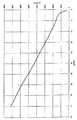
なお、図8には、上記のような回路定数による改善が行われていない電源装置におけるデューティ値に対する出力電圧値の特性(“従来回路での特性”)と、上記のような回路定数による改善が行われた電源装置におけるデューティ値に対する出力電圧値の特性(“回路定数改善後の特性”)との一例を示してある。ここで、同図中の横軸はデューティ値(%)を示し、縦軸は出力電圧値(V)を示している。
【0020】
しかしながら、上記のような従来例に係るスナバ回路を用いた構成では、以下で説明するように、例えばスナバ回路での損失(熱損失)が大きくなり、効率が非常に悪くなってしまうといった不具合があった。また、このような構成では、例えばスナバ回路の形状等が大きくなってしまうといった不具合も生じてしまう。
【0021】
また、上記文献1には、デューティ値と出力値との特性を予め記憶しておき、その特性に応じて制御量を演算して制御を行う方法が記載されている。この方法を用いると、例えばソフト制御を行うに際して制御方法が複雑になるという問題は解消されるものの、リップルが大きくなったり所望の出力電圧からの乖離が大きくなるという問題には効果が期待できない。
【0022】
次に、上記のような従来例に係るスナバ回路を用いた電源装置における不具合を更に詳しく説明する。
まず、電源装置がスナバ回路を含まない場合に、PWM信号のデューティ値と出力電圧値との特性が正比例の関係にならない理由を説明する。
【0023】
図9には、スナバ回路を含まないデジタル制御方式を用いた電源装置を構成する高圧電源部の回路構成例を示してある。
すなわち、例えば上記図6(a)に示した電源装置と同様に、高圧電源部は、トランス71やスイッチ素子72や整流平滑回路73や電圧検出回路74や電流検出回路75から構成されている。また、同図中の“Vin”は直流電源からの入力電圧(例えば24V)を示し、“PWM”はパルス発振器からのPWM信号を示し、“GND”や“AGND”はグラウンド(接地)を示し、“Imon”は電流検出回路75により検出される電流値を示し、“Vmon”は電圧検出回路74により検出される電圧値を示している。
【0024】
なお、本明細書の図面中では、上記図9中に“K1”で示した記号により抵抗を表し、“K2”で示した記号によりトランジスタを表し、“K3”で示した記号によりコンデンサを表し、“K4”で示した記号によりダイオードを表し、“K5”で示した記号により演算増幅器(OP Amp)を表すこととし、“K1”等の符号が付されていないものについても、同じ記号は同じ回路素子(但し、抵抗値等といった回路定数等は同じでなくともよい)を表すものとする。
【0025】
また、図10には、上記図9に示したトランス71部分の等価回路例を示してあり、図10中の“Rs”はトランス71の1次巻線の内部抵抗を示し、“Ls”は当該1次巻線の漏れインダクタンスを示し、“Rt”はトランス71の2次巻線の内部抵抗を示し、“Lt”は当該2次巻線の漏れインダクタンスを示し、“Lu”はトランス71の1次巻線と2次巻線との間の相互インダクタンスを示し、“Cu”は当該1次巻線と当該2次巻線との間の分布容量の合計を示している。
【0026】
同図に示されるように、例えば高圧用のトランス71の2次巻線ではその巻数が多いために、コイル間の浮遊容量が発生したり、また、様々な浮遊容量が発生したりしてしまい、これらの浮遊容量を総合したもの(分布容量と言われる)Cuを完全になくすことはできない。
また、例えばフライバック方式を用いた高圧用のトランス71では、1次巻線と2次巻線との絶縁耐圧を確保するためにボビンの構造が特殊となることから、1次巻線と2次巻線との結合が悪くなって漏れインダクタンスLs、Ltが大きくなってしまう。
【0027】
図11には、上記図9や上記図10に示した電源装置における、PWM信号のデューティ値と出力電圧値との関係の一例を示してあり、図中の横軸はデューティ値(%)を示し、縦軸は出力電圧値(−V)を示している。図11に示されるように、デューティ値に対する出力電圧値の特性の直線性は、図示される▲1▼、▲2▼、▲3▼の現象により満足されない。
【0028】
ここで、上記した▲1▼、▲2▼、▲3▼の現象をそれぞれ説明する。
まず、▲1▼の現象は、例えば或る一定の駆動周波数の入力信号(PWM信号)のオン状態の幅を広くしていくと(つまり、デューティ値を大きくしていくと)、或るポイントでまず、トランス71の1次巻線及び2次巻線による相互インダクタンスのインピーダンスω・Lu(ωは信号の角振動数)と2次巻線間等の分布容量によるインピーダンス1/(ω・Cu)とが等しくなり、これにより並列共振(1次共振)が発生してしまう現象である。
【0029】
また、▲2▼の現象は、上記▲1▼の現象が生じた後に更に、PWM信号のオン状態の幅を広くしていくと次に、トランス71の1次巻線による漏れインダクタンスのインピーダンスω・Lsと2次巻線間等の分布容量によるインピーダンス1/(ω・Cu)とが等しくなり、これにより、直列共振(2次共振)が発生してしまう現象である。
【0030】
これら▲1▼、▲2▼の現象が生じるところでは、例えばスイッチ素子72がオフである時にトランス71の1次巻線にフライバック電圧が発生し、当該フライバック電圧によるエネルギーが2次巻線側へ伝達完了されるまでは、1次巻線間に共振電流が流れてしまう。この場合、例えばスナバ回路を設けていない状態では、スイッチ素子72がオフである時に巻線間に高いフライバック電圧が発生して異常共振電流が流れてしまう。この結果、例えばPWM信号のデューティ値を変化(例えば、大きく)させても、出力電圧値の変化量(例えば、増加量)は通常よりも小さくなってしまう。
【0031】
また、▲3▼の現象は、トランス71の1次巻線の励磁インダクタンスと当該トランス71の浮遊容量とによる共振電流によりリンギング電圧が発生してしまう現象である。
この▲3▼の現象が生じるところでは、トランス71の1次巻線側の電流がリニアに変化せず、PWM信号のデューティ値の変化量(例えば、増加量)と出力電圧値の変化量(例えば、増加量)とが直線的にならずに揺れてしまう。
【0032】
つまり、電源装置ではトランス71の1次巻線側に印加したエネルギー(トランス71にかかる電圧と流れる電流)を変換して2次巻線側へ出力しており、この出力はトランス71にかかる電圧と流れる電流により決まる。そして、例えば理想的な回路を考えると、スイッチ素子がオン状態である間にトランスに流れる電流は図12(b)に示される理想的な電流のように時間経過に対して比例して上昇することから出力電圧も比例して増加するが、実際の回路では、同図(a)に示されるような共振電流(リンギング電流)が発生してしまい、トランス71に流れる電流が同図(c)に示されるように当該共振電流の影響で波打って直線性がなくなってしまう。
【0033】
次に、電源装置が従来例に係るスナバ回路を含んでいる場合に、PWM信号のデューティ値と出力電圧値との特性の直線性が改善されることを説明し、更に、従来例に係るスナバ回路の不具合を説明する。
【0034】
図13には、従来例に係るスナバ回路を含んだデジタル制御方式を用いた電源装置を構成する高圧電源部の回路構成例を示してあり、この構成は、トランス71の1次巻線間に1つの抵抗(スナバ抵抗)76がスナバ回路として挿入されて備えられている点を除いては、例えば上記図9に示した構成と同様である。
また、図14には、上記図13に示したトランス71部分の等価回路例を示してあり、この等価回路は、上記のようにトランス71の1次巻線の両端にスナバ抵抗76が備えられている点を除いては、例えば上記図10に示したものと同様である。
【0035】
このようにスナバ抵抗76を備えた構成では、例えば上記▲1▼の現象や上記▲2▼の現象に対しては、トランス71の1次巻線側のインピーダンスを低下させてフライバック電圧を低下させることができ、これにより、異常共振電流を或るレベルまで抑えることができ、並列共振や直列共振の影響を抑えることができる。つまり、この構成では、上記した1次共振や2次共振が発生してしまうポイントを制御範囲を超えた出力電圧値のポイント(すなわち、使用範囲を超えるほどに大きいデューティ値に対応した出力電圧値の範囲)にずらすことができる。
【0036】
また、このようにスナバ抵抗76を備えた構成では、例えば上記▲3▼の現象に対しては、トランス71の1次巻線側のインピーダンスを低下させることができ、例えばインダクタンス(L)と容量(C)による共振に対して抵抗(ここでは、スナバ抵抗76)を挿入することでそのLC間のエネルギーを当該抵抗の抵抗値(R)で消費して抑えることができることから、リンギング電圧を抑えることができる。
【0037】
このように、従来例に係るスナバ抵抗76を備えた電源装置では、PWM信号のデューティ値と出力電圧値との特性の直線性を改善することができる。
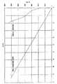
ここで、図15には、上記図13や上記図14に示した従来例に係るスナバ抵抗76を備えた電源装置における、PWM信号のデューティ値と出力電圧値との関係の一例を示してあり、図中の横軸はデューティ値(%)を示し、縦軸は出力電圧値(−V)を示している。図15に示されるように、デューティ値に対する出力電圧値の特性の直線性は、スナバ抵抗76により改善されている。
【0038】
しかしながら、上記した1つのスナバ抵抗76から構成される従来例に係るスナバ回路を用いた場合には、上記したように、例えばトランス71の1次巻線間に挿入した当該スナバ抵抗76における損失が大きくなり効率が悪くなるといった不具合や、例えばスナバ抵抗の形状等が大きくなってしまうといった不具合が生じていた。
【0039】
具体的には、上記図13や上記図14に示した電源装置のように1つのスナバ抵抗76をトランス71の1次巻線間に挿入する構成では、当該スナバ抵抗76の抵抗値を上記したフライバック電圧の抑制と上記したリンギング電圧の抑制とのいずれの抑制にとっても必要十分なインピーダンス(すなわち、低抵抗)に設定することが必要である。通常は、リンギング電圧の抑制のためのインピーダンスの方がフライバック電圧の抑制のためのインピーダンスと比べて小さいため、上記したスナバ抵抗76の抵抗値をリンギング電圧の抑制のための値に設定する。
【0040】
すると、フライバック電圧の抑制においては必要以上に低インピーダンスとなってしまうことから、これが発熱(熱損失)の原因となってしまっていた。
また、このようなスナバ回路の構成では、スナバ抵抗76自体の形状が比較的大きくなってしまい、また、多くの熱を放出させる必要があるためにスイッチング素子に係る放熱部品が必要となることから、電源装置全体としての形状が大きくなってしまっていた。
【0041】
【発明が解決しようとする課題】
上述のように、従来のデジタル制御方式を用いた電源装置では、例えば上記従来例に係るスナバ回路を備えた場合であっても、当該スナバ回路における損失が大きくなり効率が悪くなるといった不具合や、当該スナバ抵抗の形状等が大きくなってしまうといった不具合があった。
【0042】
本発明は、このような従来の課題を鑑みてなされたもので、トランスの1次巻線に接続されたスイッチング回路によるスイッチングにより2次巻線に出力電圧を得るに際して、例えばPWM信号のデューティ値に対する出力電圧値の特性がリニアになるように改善するとともに、装置内部における熱損失を抑えて高効率を実現することができる電源装置を提供することを目的とする。
【0043】
【課題を解決するための手段】
上記目的を達成するため、本発明に係る電源装置では、入力電圧が一端に印加される1次巻線と2次巻線とを有するトランスと、1次巻線の他端に直列に接続されたスイッチング回路とを備え、当該スイッチング回路によるスイッチングにより2次巻線に出力電圧を得るに際して、1次巻線に対して、リンギング電圧を抑制する抵抗値を有した抵抗と入力電圧に順方向なダイオードとを直列に接続した第1の直列回路と、フライバック電圧を抑制する抵抗値を有した抵抗と入力電圧に逆方向なダイオードとを直列に接続した第2の直列回路とを並列に設けた。
【0044】
従って、リンギング電圧(上記▲3▼の現象)を抑制するためのスナバ回路に相当する第1の直列回路と、フライバック電圧(上記▲1▼、▲2▼の現象)を抑制するためのスナバ回路に相当する第2の直列回路とが別個に設けられるため、リンギング電圧抑制用の抵抗値とフライバック電圧抑制用の抵抗値とをそれぞれ適した値に設定することができ、これにより、例えばスイッチングによる出力電圧値の特性が当該スイッチングに係るデューティ値(例えば上記したPWM信号のデューティ値)に対してリニアになるように改善することができるとともに、装置内部における熱損失を抑えて高効率を実現することができる。
【0045】
また、本発明に係る電源装置では、入力電圧が一端に印加される1次巻線と2次巻線とを有するトランスと、1次巻線の他端に直列に接続されたスイッチング回路とを備え、当該スイッチング回路によるスイッチングにより2次巻線に出力電圧を得るに際して、1次巻線に対して、リンギング電圧を抑制する抵抗値を有した抵抗と入力電圧に順方向なダイオードとを直列に接続した第1の回路と、フライバック電圧を抑制する抵抗値を有した抵抗を備えた第2の回路とを並列に設けた。
【0046】
従って、リンギング電圧(上記▲3▼の現象)を抑制するためのスナバ回路に相当する第1の回路と、フライバック電圧(上記▲1▼、▲2▼の現象)を抑制するためのスナバ回路に相当する第2の回路とが別個に設けられるため、リンギング電圧抑制用の抵抗値とフライバック電圧抑制用の抵抗値とをそれぞれ適した値に設定することができ、これにより、例えばスイッチングによる出力電圧値の特性が当該スイッチングに係るデューティ値(例えば上記したPWM信号のデューティ値)に対してリニアになるように改善することができるとともに、装置内部における熱損失を抑えて高効率を実現することができる。
【0047】
【発明の実施の形態】
本発明に係る一実施例を図面を参照して説明する。
なお、本発明に係る電源装置はデジタル制御に適したものであり、本例では、デジタル制御方式を用いた電源装置に本発明を適用した場合を示す。また、本例では、例えば数100Vから数10kVといった高電圧を発生させる高圧電源装置に本発明を適用した場合を例として示すが、本発明は他の電源装置に適用することも可能なものである。
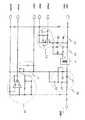
【0048】
図1は本例に係る高圧電源装置のブロック図であり、本例の高圧電源装置は、トランス(例えばフライバック方式を用いた高圧用の昇圧トランス)11やスイッチング回路12や第1スナバ回路13や第2スナバ回路14や整流平滑回路15や電圧検出回路16や電流検出回路17を備えた高圧電源部1と、直流電源2と、A/D変換器21やCPU22やパルス発振器24を備えた主制御部3とから構成されており、主制御部3により目標値に制御される電圧を高圧電源部1から負荷4へ供給する構成となっている。
【0049】
また、後述するように、各スナバ回路13、14はそれぞれ、抵抗Ra、RbとダイオードDa、Dbとを直列に接続して構成されている。また、CPU22は演算器23を備えている。
ここで、直流電源2は例えば所定の直流電力(本例では、所定の直流電圧による電圧及び電流)を生成して高圧電源部1へ出力する機能を有しており、高圧電源部1は入力電力から負荷4へ供給するための高圧電力を生成して当該高圧電力を負荷4へ出力する機能を有しており、主制御部3はスイッチング回路12の制御等を行って装置全体の動作を司る機能を有している。
【0050】
高圧電源部1に備えられたトランス11の1次巻線の一端には直流電源2の出力端が接続されており当該直流電源2により生成される所定の電圧値(例えば24V)の入力電圧Vinが印加されているとともに、当該1次巻線の他端にはスイッチング回路12中のスイッチ素子(本例では、後述するようにトランジスタ)の出力端が接続されている。
【0051】
また、トランス11と直流電源2やスイッチング回路12との間には、トランス11の1次巻線の両端に、共振電流抑制回路として第1スナバ回路13と第2スナバ回路14とが並列に接続されている。そして、スイッチング回路12によるスイッチングによりトランス11の2次巻線に出力電圧(本例では、入力電圧を昇圧したもの)が得られる。
また、トランス11の2次巻線の端子には整流平滑回路15の入力端が接続されており、当該整流平滑回路15は当該2次巻線に誘起される交流電圧(交流電流)を整流して平滑することにより、トランス11の2次巻線側で所望の出力波形を生成する。
【0052】
整流平滑回路15の3つの出力端のそれぞれには負荷4及び電圧検出回路16及び電流検出回路17が接続されており、負荷4へは電力が供給され、電圧検出回路16では負荷4へ供給される電圧値に対応した電圧値(例えば1/1000の値など)を出力状態量として検出して当該検出値である電圧モニター値Vmonを示す電圧モニター信号を主制御部3へ送り、電流検出回路17では負荷4へ供給される電流値に対応した電流値を出力状態量として検出して当該検出値である電流モニター値Imonを示す電流モニター信号を主制御部3へ送る。
【0053】
なお、本例では、CPU22による制御が行われるため、電圧検出回路16では当該CPU22により演算することが可能な電圧レベル(例えば0V〜5V)の範囲に収まるようにして検出電圧値を主制御部3へ送る。
また、負荷4へ供給すべき電圧としては、例えば負荷の使用状況等に応じて、グラウンドに対して正の電圧である場合や負の電圧である場合があるが、本例では、正の電圧を負荷4へ供給する場合を例として説明を行う。
【0054】
また、主制御部3に備えられたA/D変換器21の2つの入力端にはそれぞれ電圧検出回路16の出力端及び電流検出回路17の出力端が接続されており、当該A/D変換器21では、電圧検出回路16により生成された電圧モニター信号を当該信号が示す電圧モニター値Vmonへアナログ−デジタル変換してCPU22へデジタル値として出力するとともに、電流検出回路17により生成された電流モニター信号を当該信号が示す電流モニター値Imonへアナログ−デジタル変換してCPU22へデジタル値として出力する。
【0055】
CPU22に備えられた演算器23の入力端はA/D変換器21の出力端に接続されており、当該演算器23では、入力されたモニター値(例えば電圧モニター値Vmon或いは電流モニター値Imon)と高圧電源が制御されるべき目標値(例えば予め設定された値)とを比較して、当該比較結果に基づいて当該モニター値が当該目標値に一致するようにパルス発振器24から発振されるPWM信号の最適なデューティ値を演算し、そして、当該最適なデューティ値のPWM信号が発振されるようにパルス発振器24を制御する。
【0056】
パルス発振器24の入力端には演算器23の出力端が接続されているとともに、当該パルス発振器24の出力端にはスイッチング回路12の入力端が接続されており、パルス発振器24では、演算器23により制御されるデューティ値を有したPWM信号を発振して当該PWM信号(PWM)をスイッチング回路12へ出力する。なお、パルス発生器24では、例えばデューティ値が可変な一定の周期の連続パルスをスイッチングパルス(PWM信号)として発生する。
【0057】
スイッチング回路12は、入力されるPWM信号のオンオフに応じてオンオフ(断続)されることによりトランス11の1次巻線側の印加電圧(1次巻線に供給される電流)を周期的にスイッチングし、これにより、当該PWM信号のデューティ値に応じた大きさの出力電力(出力電圧や出力電流)がトランス11の2次巻線から得られる。そして、上記と同様なCPU22によるフィードバック制御が繰り返されることにより、出力電圧や出力電流の値が目標値に制御される。
【0058】
次に、図2には、本例の高圧電源装置を構成する高圧電源部1の具体的な回路構成例を示してある。
なお、同図中の“Vin”は直流電源2からの入力電圧(例えば24V)を示し、“PWM”はパルス発振器24からのPWM信号を示し、“GND”や“AGND”はグラウンド(接地)を示し、“Imon”は電流検出回路17により検出される電流値を示し、“Vmon”は電圧検出回路16により検出される電圧値を示している。
【0059】
第1スナバ回路13は、直列接続された抵抗RaとダイオードDaとから構成されており、具体的には、直流電源2とトランス11の1次巻線の一端とを接続するラインと抵抗Raの一端とが接続され、当該抵抗Raの他端とダイオードDaのアノード端子とが接続され、当該ダイオードDaのカソード端子と後述するトランジスタ(スイッチ素子)Q1のドレイン端子とが接続されている。このような構成を有する第1スナバ回路13では、例えば上記従来例に示したリンギング電圧(上記▲3▼の現象)を抑制することができる。
【0060】
また、第2スナバ回路14は、上記した第1スナバ回路13とはダイオードの向きが逆向きに直列接続された抵抗RbとダイオードDbとから構成されており、トランス11の1次巻線に対して、上記した第1スナバ回路13と並列に接続されて設けられている。具体的には、直流電源2とトランス11の1次巻線の一端とを接続する前記ラインと抵抗Rbの一端とが接続され、当該抵抗Rbの他端とダイオードDbのカソード端子とが接続され、当該ダイオードDbのアノード端子と後述するトランジスタ(スイッチ素子)Q1のドレイン端子とが接続されている。このような構成を有する第2スナバ回路14では、例えば上記従来例に示したフライバック電圧(上記▲1▼、▲2▼の現象)を抑制することができる。
【0061】
また、第1スナバ回路13を構成する抵抗Raの抵抗値としては、リンギング電圧を抑制するのに適した値(例えば440Ω)が設定され、第2スナバ回路14を構成する抵抗Rbの抵抗値としては、フライバック電圧を抑制するのに適した値(例えば4.7kΩ)が設定される。
また、上記したダイオードDaやダイオードDbは、例えばカソード端子側と比べてアノード端子側に高電圧が印加された場合にアノード端子側からカソード端子側へ電流を流す一方、カソード端子側と比べてアノード端子側に低電圧が印加された場合には電流を流さない機能を有している。
【0062】
具体的に、本例の場合には、直流電源2からの入力電圧が正であり、当該入力電圧と同じ方向の電圧によって(すなわち、スイッチ素子Q1がオン状態の時に)第1スナバ回路13に電流が流れ、当該入力電圧とは異なる方向(逆の方向)の電圧によって(すなわち、スイッチ素子Q1がオフ状態の時に)第2スナバ回路14に電流が流れる構成となっている。つまり、本例では、第1スナバ回路13のダイオードDaは入力電圧に対して順方向に設けられており、第2スナバ回路14のダイオードDbは入力電圧に対して逆方向に設けられている。
【0063】
スイッチング回路12は、例えば電界効果トランジスタ(FET)Q1や2つの抵抗R1、R2から構成されており、具体的には、スイッチング素子であるFETQ1のドレイン端子がトランス11の1次巻線の他端及びダイオードDaのカソード端子及びダイオードDbのアノード端子に接続されており、当該FETQ1のゲート端子が抵抗R1を介してパルス発振器24の出力端に接続されており、当該FETQ1のソース端子がグラウンドに接続されており、前記ゲート端子と前記ソース端子とが抵抗R2を介して接続されている。
【0064】
このような構成を有するスイッチング回路12では、パルス発振器24により生成されるPWM信号がFETQ1のゲート端子に入力され、例えば当該PWM信号がハイ(High)レベルである時にFETQ1がオン状態へ切り替えられる一方、当該PWM信号がロウ(Low)レベルである時にFETQ1がオフ状態へ切り替えられる。そして、スイッチング回路12では、PWM信号のデューティ値に応じた期間でFETQ1のオン/オフの状態が交互に繰り返されることにより、当該デューティ値に応じた期間でトランス11の1次巻線への電力の印加/非印加を交互に行うことができる。
【0065】
整流平滑回路15は、例えば2つのダイオードD1、D2や2つのコンデンサC1、C2から構成されており、具体的には、トランス11の2次巻線の一端にダイオードD1のカソード端子及びダイオードD2のアノード端子が接続されており、ダイオードD1のアノード端子にコンデンサC1の一端及び負荷4への抵抗及び電圧検出回路16への抵抗が接続されており、ダイオードD2のカソード端子にコンデンサC2の一端及び電流検出回路17の入力端が接続されており、トランス11の2次巻線の他端にコンデンサC1の他端及びコンデンサC2の他端が接続されている。
【0066】
このような構成を有する整流平滑回路15では、トランス11の2次巻線に誘起される交流電流をダイオードD1、D2とコンデンサC1、C2との組合せによって整流して平滑することができ、このようにして整流及び平滑した電力を負荷4へ供給することができる。
【0067】
また、電圧検出回路16は、例えば演算増幅器(OP Amp)や2つの抵抗(例えば1つは可変抵抗)や2つのコンデンサから構成されており、整流平滑回路15から自己へ出力される電圧の電圧値を電圧モニター値VmonとしてA/D変換器21へ常時通知する構成となっている。
また、電流検出回路17は、2つの抵抗(例えば1つは可変抵抗)やコンデンサから構成されており、整流平滑回路15から自己へ流れる電流の電流値を電流モニター値ImonとしてA/D変換器21へ常時通知する構成となっている。
【0068】
また、図3には、上記図2に示したトランス11部分の等価回路例を示してあり、図3中の“Rp”はトランス11の1次巻線の内部抵抗を示し、“Lp”は当該1次巻線の漏れインダクタンスを示し、“Rq”はトランス11の2次巻線の内部抵抗を示し、“Lq”は当該2次巻線の漏れインダクタンスを示し、“L”はトランス11の1次巻線と2次巻線との間の相互インダクタンスを示し、“Co”は当該1次巻線と当該2次巻線との間の分布容量の合計を示している。
【0069】
同図に示されるように、本例では、トランス11の1次巻線に対して、リンギング電圧を抑えることができる第1スナバ回路13と、フライバック電圧を抑えることができる第2スナバ回路14とが設けられているため、PWM信号のデューティ値の増加に従って負荷4への出力電圧値が直線性をもって(比例して)増加することが実現される。具体的には、本例の構成においても、例えば上記図15に示したデューティ値に対する出力電圧値の特性のように直線性が改善された特性を得ることができる。
【0070】
更に、本例では、リンギング電圧抑制用の抵抗Raの抵抗値とフライバック電圧抑制用の抵抗Rbの抵抗値とをそれぞれ独立に設定することができ、これら2つの抵抗Ra、Rbの抵抗値としてそれぞれに最適な異なる値を設定することにより、例えば従来例に係るスナバ回路(つまり、リンギング電圧抑制とフライバック電圧抑制とに共通な1つのスナバ抵抗)を用いた場合と比べて、無駄な電力消費を抑えることができる。
【0071】
具体的には、通常、リンギング電圧抑制用のインピーダンスは比較的小さい値である必要があり、これと比べて、フライバック電圧抑制用のインピーダンスは非常に大きい値であるのが好ましいことから、本例では、好ましい一例として、リンギング電圧抑制用の抵抗Raの抵抗値として440Ωを設定し、フライバック電圧抑制用の抵抗Rbの抵抗値として4.7kΩを設定してある。
【0072】
この場合、抵抗にかかる電圧Vと当該抵抗を流れる電流Iと当該抵抗の抵抗値Rとの関係がV=R・Iと表されて、当該抵抗で消費される電力PがP=V・Iと表されることから、例えばリンギング電圧抑制用の第1スナバ回路13での消費電力は従来例と同様に比較的大きいものの、フライバック電圧抑制用の第2スナバ回路14での消費電力は例えば従来例と比べて非常に小さくすることができ、全体として、消費電力の削減を実現することができる。
【0073】
なお、これに対して、従来例にかかるスナバ回路(スナバ抵抗)では例えば当該スナバ抵抗の抵抗値が440Ωに設定されることになり、つまり、リンギング電圧抑制のためばかりでなくフライバック電圧抑制のためにも440Ωという小さい抵抗値が用いられてしまうことから、フライバック電圧抑制時に非常に大きい電力を無駄に消費してしまうことになる。
【0074】
以上のように、本例の高圧電源装置では、トランス11の1次巻線に対して、リンギング電圧を抑制する抵抗値を有した抵抗Raと入力電圧Vinに順方向なダイオードDaとを直列に接続した第1スナバ回路13(本発明に言う第1の直列回路に相当するもの)と、フライバック電圧を抑制する抵抗値を有した抵抗Rbと入力電圧Vinに逆方向なダイオードDbとを直列に接続した第2スナバ回路14(本発明に言う第2の直列回路に相当するもの)とを並列に設けた。
【0075】
従って、本例の高圧電源装置では、例えばデジタル制御方式によりPWM信号のデューティ値をフィードバック制御するに際して、PWM信号のデューティ値に対する出力電圧値の特性がリニアになるように改善することができて、例えば出力電圧値の全範囲において安定した出力電圧を得ることができるとともに、例えば従来例に係るスナバ回路のように必要以上に低インピーダンスの抵抗を用いる必要がないため、スナバ回路(本例では、特に、第2スナバ回路14)での熱損失を抑えることができ、これにより、装置内部における熱損失を抑えて高効率を実現することができる。
【0076】
また、本例の高圧電源装置では、上記のように出力効率が向上することから、例えば直流電源2から高圧電源部1に入力される電流を低減させることも可能であり、これによりスイッチング素子Q1での発熱を抑えることもできるため、装置の低コスト化等を実現することもできる。
また、本例のような構成では、例えばスナバ抵抗そのものの形状を小さくすることも可能であり、また、スイッチ素子Q1の放熱部品を省略することが可能であること等により装置全体の形状を小さくすることもできる。
【0077】
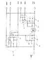
次に、図4及び図5を参照して、本発明に係る他の実施例を説明する。なお、本例では、高圧電源装置に本発明を適用した場合を示す。
ここで、図4は本例に係る高圧電源装置のブロック図であり、図5には本例の高圧電源装置を構成する高圧電源部1の具体的な回路構成例を示してある。なお、本例の高圧電源装置の構成は、第2スナバ回路14aの構成が異なる点を除いては、例えば上記図1〜上記図3を用いて説明した高圧電源装置の構成と同様であり、当該高圧電源装置を改良したものである。このため、本例では、上記図1〜上記図3を用いて説明した高圧電源装置と同様な構成や動作については詳しい説明を省略することとし、また、同様な構成部分については上記図1〜上記図3で用いたものと同じ符号を用いて示す。
【0078】
上述のように、本例の高圧電源装置では、フライバック電圧抑制用である第2スナバ回路14aの構成が上記図1〜上記図3を用いて説明した高圧電源装置とは異なっている。
すなわち、本例の第2スナバ回路14aは、抵抗Rbから構成されており、トランス11の1次巻線に対して、第1スナバ回路13と並列に接続されて設けられている。具体的には、直流電源2とトランス11の1次巻線の一端とを接続するラインと抵抗Rbの一端とが接続され、当該抵抗Rbの他端とトランジスタ(スイッチ素子)Q1のドレイン端子とが接続されている。このような構成を有する第2スナバ回路14aでは、例えば上記従来例に示したフライバック電圧(上記▲1▼、▲2▼の現象)を抑制することができる。
【0079】
また、第1スナバ回路13を構成する抵抗Raの抵抗値としては、リンギング電圧を抑制するのに適した値(例えば440Ω)が設定され、第2スナバ回路14aを構成する抵抗Rbの抵抗値としては、フライバック電圧を抑制するのに適した値(例えば4.7kΩ)が設定される。
また、上記したダイオードDaは、例えばカソード端子側と比べてアノード端子側に高電圧が印加された場合にアノード端子側からカソード端子側へ電流を流す一方、カソード端子側と比べてアノード端子側に低電圧が印加された場合には電流を流さない機能を有している。
【0080】
具体的に、本例の場合には、直流電源2からの入力電圧が正であり、当該入力電圧と同じ方向の電圧によって(すなわち、スイッチ素子Q1がオン状態の時に)第1スナバ回路13及び第2スナバ回路14aに電流が流れ、当該入力電圧とは異なる方向(逆の方向)の電圧によって(すなわち、スイッチ素子Q1がオフ状態の時に)第2スナバ回路14aに電流が流れる構成となっている。つまり、本例では、第1スナバ回路13のダイオードDaは入力電圧に対して順方向に設けられている。
【0081】
本例では、リンギング電圧抑制用の抵抗Raの抵抗値とフライバック電圧抑制用の抵抗Rbの抵抗値とをそれぞれ独立に設定することができ、これら2つの抵抗Ra、Rbの抵抗値としてそれぞれに最適な異なる値を設定することにより、例えば従来例に係るスナバ回路(つまり、リンギング電圧抑制とフライバック電圧抑制とに共通な1つのスナバ抵抗)を用いた場合と比べて、無駄な電力消費を抑えることができる。
【0082】
具体的には、通常、リンギング電圧抑制用のインピーダンスは比較的小さい値である必要があり、これと比べて、フライバック電圧抑制用のインピーダンスは非常に大きい値であるのが好ましいことから、本例では、好ましい一例として、リンギング電圧抑制用の抵抗Raの抵抗値として440Ωを設定し、フライバック電圧抑制用の抵抗Rbの抵抗値として4.7kΩを設定してある。
【0083】
ここで、抵抗にかかる電圧Vと当該抵抗を流れる電流Iと当該抵抗の抵抗値Rとの関係がV=R・Iと表されて、当該抵抗で消費される電力PがP=V・Iと表される。
本例では、フライバック電圧抑制用の第2スナバ回路14aの抵抗Rbのみに電流が流れる時と、リンギング電圧抑制用の第1スナバ回路13の抵抗Raとフライバック電圧抑制用の第2スナバ回路14aの抵抗Rbとの両方に電流が流れる時とがある。
【0084】
つまり、本例では、リンギング電圧抑制用の抵抗Raの抵抗値がフライバック電圧抑制用の抵抗Rbの抵抗値と比べて非常に小さいインピーダンスであることから、例えばフライバック電圧の抑制時には第1スナバ回路13側(抵抗Ra)には導通させないようにしてその時のインピーダンスを抵抗Rbの抵抗値(本例では、4.7kΩ)とする一方、例えばリンギング電圧の抑制時には第1スナバ回路13(抵抗Ra)及び第2スナバ回路14a(抵抗Rb)の両方に導通させるようにしてその時のインピーダンスをR={(抵抗Raの抵抗値)×(抵抗Rbの抵抗値)}/{(抵抗Raの抵抗値)+(抵抗Rbの抵抗値)}としている。
【0085】
ここで、前記Rは2つの抵抗Ra、Rbを並列接続した場合の合成抵抗であり、本例では、抵抗Ra=440Ωであって、抵抗Rb=4.7kΩであるとすると、前記Rは約402Ωとなる。
以上のように、本例の高圧電源装置においても、例えば上記図1〜上記図3を用いて説明した高圧電源装置と同様な効果を得ることができ、更に、本例の構成では、例えば上記図1〜上記図3を用いて説明した高圧電源装置と比べて、第2スナバ回路14aに関してダイオードを1つ減少させることができる。
【0086】
ここで、本発明に係る電源装置の構成としては、必ずしも以上の実施例に示したものに限られることはなく、種々な構成が用いられてもよい。
また、本発明に係る電源装置は、種々な分野の電源装置として適用可能なものであるが、例えば電子写真方式のプリンタや複写機等に備えられる電源装置のように高圧や高精度や広範囲での電圧可変が要求されるものに適用されて好適なものであり、例えばCRTディスプレイの電源装置等に適用することも可能なものである。
【0087】
【発明の効果】
以上説明したように、本発明に係る電源装置によると、入力電圧が一端に印加される1次巻線と2次巻線とを有するトランスと、1次巻線の他端に直列に接続されたスイッチング回路とを備え、当該スイッチング回路によるスイッチングにより2次巻線に出力電圧を得るに際して、1次巻線に対して、リンギング電圧を抑制する抵抗値を有した抵抗と入力電圧に順方向なダイオードとを直列に接続した第1の直列回路と、フライバック電圧を抑制する抵抗値を有した抵抗と入力電圧に逆方向なダイオードとを直列に接続した第2の直列回路とを並列に設けたため、例えばスイッチングによる出力電圧値の特性が当該スイッチングに係るデューティ値(例えば上記したPWM信号のデューティ値)に対してリニアになるように改善することができるとともに、装置内部における熱損失を抑えて高効率を実現することができる。
【0088】
また、本発明に係る電源装置では、入力電圧が一端に印加される1次巻線と2次巻線とを有するトランスと、1次巻線の他端に直列に接続されたスイッチング回路とを備え、当該スイッチング回路によるスイッチングにより2次巻線に出力電圧を得るに際して、1次巻線に対して、リンギング電圧を抑制する抵抗値を有した抵抗と入力電圧に順方向なダイオードとを直列に接続した第1の回路と、フライバック電圧を抑制する抵抗値を有した抵抗を備えた第2の回路とを並列に設けたため、例えばスイッチングによる出力電圧値の特性が当該スイッチングに係るデューティ値(例えば上記したPWM信号のデューティ値)に対してリニアになるように改善することができるとともに、装置内部における熱損失を抑えて高効率を実現することができる。
【図面の簡単な説明】
【図1】本発明の一実施例に係る高圧電源装置のブロック図である。
【図2】本発明の一実施例に係る高圧電源装置の回路構成例を示す図である。
【図3】トランス部の等価回路例を示す図である。
【図4】 本発明の他の実施例に係る高圧電源装置のブロック図である。
【図5】 本発明の他の実施例に係る高圧電源装置の回路構成例を示す図である。
【図6】従来例に係る電源装置の構成例を示す図である。
【図7】PWM信号のデューティ値の可変幅に関する問題を説明するための図である。
【図8】PWM信号のデューティ値と出力電圧値との関係の一例を示す図である。
【図9】スナバ回路を含まない電源装置の回路構成例を示す図である。
【図10】トランス部の等価回路例を示す図である。
【図11】PWM信号のデューティ値と出力電圧値との関係の一例を示す図である。
【図12】共振電流による電流波形を説明するための図である。
【図13】スナバ回路を含んだ電源装置の回路構成例を示す図である。
【図14】トランス部の等価回路例を示す図である。
【図15】PWM信号のデューティ値と出力電圧値との関係の一例を示す図である。
【符号の説明】
1・・高圧電源部、 2・・直流電源、 3・・主制御部、 4・・負荷、
11・・トランス(昇圧トランス)、 12・・スイッチング回路、
13・・第1スナバ回路、 14、14a・・第2スナバ回路
15・・整流平滑回路、 16・・電圧検出回路、 17・・電流検出回路、
21・・A/D変換器、 22・・CPU、 23・・演算器、
24・・パルス発振器、 Ra、Rb、R1、R2、Rp、Rq・・抵抗、
Da、Db、D1、D2・・ダイオード、 Q1・・FET、
C1、C2・・コンデンサ、 Lp、Lq、L・・インダクタンス、
Co・・容量、 K1・・抵抗、 K2・・トランジスタ、
K3・・コンデンサ、 K4・・ダイオード、 K5・・演算増幅器、[0001]
BACKGROUND OF THE INVENTION
The present invention relates to a power supply apparatus that can be used as a high-voltage power supply apparatus in an image forming apparatus such as an electrophotographic printer or a copying machine.
[0002]
[Prior art]
For example, high-voltage power supplies such as electrophotographic printers and copiers are used to apply a specified voltage or current to the load around the photoconductor. The functions of the load are generally charging, developing, transferring, Functions such as peeling and cleaning.
In addition, information on the timing for supplying output to each load and information on the output potential are sent from, for example, a control board that performs process control to the high-voltage power supply, and the high-voltage power supply outputs according to the information.
[0003]
For this reason, it is possible to change the output value of the high-voltage power supply by changing the output potential information sent from the control board to the high-voltage power supply, so that the high-voltage power supply supplies the desired output to the load in response to the process request. To do. In addition, today, the variable output range required for high-voltage power supplies has been widespread due to high accuracy and high functionality such as color and image quality, and has, for example, an output variable region of about 10 times. ing. As a specific example, when the output value (direct current or alternating current) given to the load around the drum (for charging, development, or transfer) is changed according to the print density or the like, a wide range (for example, transfer) It is necessary to change the output of 500V to 4kV.
[0004]
As a method for controlling the high-voltage power output described above, not only analog control controlled by an operational amplifier (OP Amp) or the like, but also a power supply device using digital control as described in, for example, Japanese Patent Application Laid-Open No. 62-279366 In such a digital control system, a high-voltage power supply output is arithmetically controlled by a CPU (Central Processing Unit), an ASIC (Application Specific Integrated Circuit), or the like.
[0005]
As a method for calculating the output value to be controlled, for example, switching described later is performed based on the result of comparing the detected value detected by the detecting means with the output state quantity from the high-voltage power supply and the target value corresponding to the variable output. A method of controlling the value of the duty of a pulse width modulation (PWM) signal to be given to the means is used.
[0006]
Specifically, FIG. 6A shows a configuration example of a power supply device using a digital control method. In this power supply apparatus, a
[0007]
That is, the
[0008]
The duty value is, for example, an on-state period (one on-state time width plus one off-state time width) as T, and an on-state time width within one period (T). Where t is t / T. When digital control is used, the accuracy of control is usually improved as the minimum amount (the minimum variable width in the ON state) that can change the duty value is smaller.
[0009]
The output from the secondary winding of the
Further, the voltage detection circuit (detection means) 35 detects a voltage value (for example, a value of 1/1000) Vmon corresponding to the voltage value supplied to the
[0010]
In the
[0011]
FIG. 6B shows a configuration example of a power supply device using an analog control method. In this power supply apparatus, analog control is performed. For example, the operations of the
[0012]
Here, in the power supply apparatus using the analog control system as shown in FIG. 6B, for example, the cost required for the
[0013]
However, the power supply apparatus using the digital control method has the following problems.
That is, in such a power supply device, as described above, the
[0014]
Here, the problem is the variable width of the duty value of the PWM signal described above. That is, for example, it can be said that the variable range of the duty value in the power supply device using the analog control method is almost infinite, but in the case of the power supply device using the digital control method, the PWM signal for driving the
[0015]
Specifically, in FIG. 7A, the frequency of the reference clock signal is 20 kHz (that is, the period is 50 μs), and 10 bits (that is, 1024 pulses) are converted into one period (that is, 51 pulses) of the PWM signal. .2 μs), a case where a PWM signal is generated is shown, and the resolution in this case is (0.098% / bit). As described above, the duty value of the PWM signal is expressed by t / T using the period of the on state (that is, the time for one period of the PWM signal) T and the time width t of one on state. The
[0016]
When digital control is used in this way, the duty period is a discretely variable value because the time width t of the on state of the PWM signal can be changed with, for example, one pulse as the minimum unit. Then, as shown in FIG. 7B, the output voltage from the power supply device also changes stepwise according to the minimum unit size (variable width) that can change the duty value. End up. If the variable range of the duty value is large, the output voltage control accuracy is deteriorated.
[0017]
In addition, for example, a conventional power supply device using an analog control method does not have the problems associated with the digital control as described above, and therefore, the relationship between the duty value and the output voltage value uses a specific linear characteristic. The desired output voltage was obtained within a small duty value range. For this reason, when the digital control method is simply applied to such a conventional power supply device, for example, there is a problem that a ripple becomes large or a deviation from a desired output voltage becomes large.
[0018]
To solve the problems associated with digital control as described above, for example, the following solution is described in the conventional example of Japanese Patent Laid-Open No. 9-149637 (hereinafter referred to as Document 1).
That is, in this example, in order to obtain a gentle and directly proportional characteristic between the duty value and the output value, a method of devising a constant of the primary side snubber circuit or devising a reactance component of the transformer is described. . By using this method, for example, a characteristic in which the relationship between the duty value and the output value is gradual and directly proportional to the entire output range can be obtained, and the output resolution (V / bit) in the variable region can be improved. it can. As a result, the fluctuation range of the output value when the duty value is changed by the minimum bit (variable width) is reduced, and the above-described problem relating to the variable width is improved.
[0019]
FIG. 8 shows the characteristic of the output voltage value with respect to the duty value (“characteristic in the conventional circuit”) in the power supply device that has not been improved by the circuit constant as described above, and the improvement by the circuit constant as described above. 2 shows an example of the characteristic of the output voltage value with respect to the duty value (“characteristic after improvement of circuit constant”) in the power supply device in which the power supply is performed. Here, the horizontal axis in the figure represents the duty value (%), and the vertical axis represents the output voltage value (V).
[0020]
However, in the configuration using the snubber circuit according to the conventional example as described above, as described below, for example, a loss (heat loss) in the snubber circuit becomes large and the efficiency becomes very bad. there were. In addition, in such a configuration, for example, the snubber circuit shape or the like becomes large.
[0021]
Further, the
[0022]
Next, a problem in the power supply device using the snubber circuit according to the conventional example as described above will be described in more detail.
First, the reason why the characteristic between the duty value of the PWM signal and the output voltage value is not directly proportional when the power supply apparatus does not include a snubber circuit will be described.
[0023]
FIG. 9 shows a circuit configuration example of a high-voltage power supply unit constituting a power supply device using a digital control system that does not include a snubber circuit.
That is, for example, as in the power supply device shown in FIG. 6A, the high-voltage power supply unit includes a
[0024]
In the drawings of this specification, a resistor is indicated by the symbol “K1” in FIG. 9, a transistor is indicated by the symbol “K2”, and a capacitor is indicated by the symbol “K3”. The symbol “K4” represents a diode, the symbol “K5” represents an operational amplifier (OP Amp), and the same symbol is used for those not labeled with “K1” or the like. The same circuit elements (however, circuit constants such as resistance values may not be the same) are used.
[0025]
FIG. 10 shows an example of an equivalent circuit of the
[0026]
As shown in the figure, for example, the secondary winding of the high-
Also, for example, in the high-
[0027]
FIG. 11 shows an example of the relationship between the duty value of the PWM signal and the output voltage value in the power supply device shown in FIG. 9 or FIG. 10, and the horizontal axis in the figure represents the duty value (%). The vertical axis represents the output voltage value (−V). As shown in FIG. 11, the linearity of the characteristic of the output voltage value with respect to the duty value is not satisfied by the phenomena (1), (2), and (3) shown in the figure.
[0028]
Here, the above phenomena (1), (2), and (3) will be described.
First, the phenomenon of {circle around (1)} is, for example, when the width of the ON state of an input signal (PWM signal) having a certain driving frequency is increased (that is, when the duty value is increased), a certain point is obtained. First, the impedance ω · Lu (ω is the angular frequency of the signal) of the mutual inductance due to the primary winding and the secondary winding of the
[0029]
Further, the phenomenon of (2) is that the impedance ω of the leakage inductance due to the primary winding of the
[0030]
Where these phenomena {circle around (1)} and {circle around (2)} occur, for example, when the
[0031]
The phenomenon (3) is a phenomenon in which a ringing voltage is generated by a resonance current caused by the exciting inductance of the primary winding of the
Where the phenomenon (3) occurs, the current on the primary winding side of the
[0032]
That is, the power supply device converts the energy applied to the primary winding side of the transformer 71 (the voltage applied to the
[0033]
Next, it will be described that the linearity of the characteristic between the duty value of the PWM signal and the output voltage value is improved when the power supply device includes the snubber circuit according to the conventional example, and further, the snubber according to the conventional example is improved. Describe the malfunction of the circuit.
[0034]
FIG. 13 shows an example of a circuit configuration of a high-voltage power supply unit constituting a power supply device using a digital control system including a snubber circuit according to a conventional example, and this configuration is arranged between primary windings of a
FIG. 14 shows an equivalent circuit example of the
[0035]
In the configuration including the
[0036]
Further, in the configuration provided with the
[0037]
Thus, in the power supply device including the
Here, FIG. 15 shows an example of the relationship between the duty value of the PWM signal and the output voltage value in the power supply device including the
[0038]
However, when the snubber circuit according to the conventional example configured by one
[0039]
Specifically, in the configuration in which one
[0040]
Then, since the impedance becomes lower than necessary in suppressing the flyback voltage, this has caused heat generation (heat loss).
Further, in such a snubber circuit configuration, the shape of the
[0041]
[Problems to be solved by the invention]
As described above, in the power supply device using the conventional digital control method, for example, even when the snubber circuit according to the above-described conventional example is provided, the loss in the snubber circuit increases and the efficiency deteriorates, There was a problem that the shape of the snubber resistor was increased.
[0042]
The present invention has been made in view of such a conventional problem. When an output voltage is obtained in the secondary winding by switching by a switching circuit connected to the primary winding of the transformer, for example, the duty value of the PWM signal is obtained. It is an object of the present invention to provide a power supply device that can improve the characteristics of the output voltage value to be linear and can achieve high efficiency by suppressing heat loss inside the device.
[0043]
[Means for Solving the Problems]
In order to achieve the above object, in a power supply device according to the present invention, a transformer having a primary winding and a secondary winding to which an input voltage is applied to one end, and the other end of the primary winding are connected in series. Switching circuit, and when the output voltage is obtained in the secondary winding by switching by the switching circuit, the primary winding has a resistance value that suppresses the ringing voltage and the input voltage has a forward direction. A first series circuit in which a diode is connected in series and a second series circuit in which a resistor having a resistance value that suppresses a flyback voltage and a diode that is opposite to the input voltage are connected in series are provided in parallel. It was.
[0044]
Therefore, the first series circuit corresponding to the snubber circuit for suppressing the ringing voltage (the phenomenon (3) above) and the snubber for suppressing the flyback voltage (the phenomena (1) and (2) above). Since the second series circuit corresponding to the circuit is separately provided, the resistance value for suppressing the ringing voltage and the resistance value for suppressing the flyback voltage can be set to appropriate values, for example, The characteristics of the output voltage value due to switching can be improved to be linear with respect to the duty value related to the switching (for example, the duty value of the PWM signal described above), and high efficiency can be achieved by suppressing heat loss inside the apparatus. Can be realized.
[0045]
In the power supply device according to the present invention, a transformer having a primary winding and a secondary winding to which an input voltage is applied to one end, and a switching circuit connected in series to the other end of the primary winding are provided. When the output voltage is obtained in the secondary winding by switching by the switching circuit, a resistor having a resistance value for suppressing the ringing voltage and a diode forward to the input voltage are connected in series to the primary winding. A connected first circuit and a second circuit having a resistor having a resistance value for suppressing the flyback voltage were provided in parallel.
[0046]
Therefore, the first circuit corresponding to the snubber circuit for suppressing the ringing voltage (the phenomenon of (3) above) and the snubber circuit for suppressing the flyback voltage (the phenomena of (1) and (2) above). Since the second circuit corresponding to is separately provided, the resistance value for suppressing the ringing voltage and the resistance value for suppressing the flyback voltage can be set to appropriate values, for example, by switching. The characteristics of the output voltage value can be improved so as to be linear with respect to the duty value related to the switching (for example, the duty value of the PWM signal described above), and high efficiency is realized by suppressing heat loss inside the apparatus. be able to.
[0047]
DETAILED DESCRIPTION OF THE INVENTION
An embodiment according to the present invention will be described with reference to the drawings.
Note that the power supply device according to the present invention is suitable for digital control, and in this example, the case where the present invention is applied to a power supply device using a digital control method is shown. In this example, the case where the present invention is applied to a high-voltage power supply device that generates a high voltage of, for example, several hundred volts to several tens kV is shown as an example. However, the present invention can also be applied to other power supply devices. is there.
[0048]
FIG. 1 is a block diagram of a high-voltage power supply device according to this example. The high-voltage power supply device of this example includes a transformer (for example, a high-voltage step-up transformer using a flyback system) 11, a switching
[0049]
Further, as will be described later, each of the
Here, the
[0050]
An output terminal of a
[0051]
Further, between the
Further, the input terminal of the rectifying / smoothing
[0052]
A load 4, a
[0053]
In this example, since the control by the
The voltage to be supplied to the load 4 may be a positive voltage or a negative voltage with respect to the ground, for example, depending on the use condition of the load. Is described as an example.
[0054]
In addition, the output terminal of the
[0055]
The input terminal of the
[0056]
The input terminal of the
[0057]
The switching
[0058]
Next, FIG. 2 shows a specific circuit configuration example of the high-voltage
In the figure, “Vin” indicates an input voltage (for example, 24 V) from the
[0059]
The
[0060]
The
[0061]
Further, as the resistance value of the resistor Ra constituting the
In addition, the diode Da and the diode Db described above, for example, flow current from the anode terminal side to the cathode terminal side when a high voltage is applied to the anode terminal side compared to the cathode terminal side, while the anodes compare to the cathode terminal side. When a low voltage is applied to the terminal side, it has a function of preventing current from flowing.
[0062]
Specifically, in the case of this example, the input voltage from the
[0063]
The switching
[0064]
In the switching
[0065]
The rectifying / smoothing
[0066]
In the rectifying and smoothing
[0067]
The
The
[0068]
3 shows an equivalent circuit example of the
[0069]
As shown in the figure, in this example, the
[0070]
Furthermore, in this example, the resistance value of the resistor Ra for suppressing the ringing voltage and the resistance value of the resistor Rb for suppressing the flyback voltage can be set independently, and the resistance values of these two resistors Ra and Rb By setting different optimal values for each, for example, compared to the case where a snubber circuit according to the conventional example (that is, one snubber resistor common to ringing voltage suppression and flyback voltage suppression) is used, wasted power Consumption can be suppressed.
[0071]
Specifically, the impedance for suppressing the ringing voltage usually needs to be a relatively small value, and it is preferable that the impedance for suppressing the flyback voltage be a very large value. In the example, as a preferable example, 440Ω is set as the resistance value of the resistor Ra for suppressing the ringing voltage, and 4.7 kΩ is set as the resistance value of the resistor Rb for suppressing the flyback voltage.
[0072]
In this case, the relationship between the voltage V applied to the resistor, the current I flowing through the resistor, and the resistance value R of the resistor is expressed as V = R · I, and the power P consumed by the resistor is P = V · I. Therefore, for example, the power consumption in the
[0073]
On the other hand, in the snubber circuit (snubber resistor) according to the conventional example, for example, the resistance value of the snubber resistor is set to 440Ω, that is, not only for suppressing the ringing voltage but also for suppressing the flyback voltage. For this reason, since a small resistance value of 440Ω is used, a very large amount of power is wasted when the flyback voltage is suppressed.
[0074]
As described above, in the high-voltage power supply device of this example, the resistor Ra having a resistance value that suppresses the ringing voltage and the diode Da forward to the input voltage Vin are serially connected to the primary winding of the
[0075]
Therefore, in the high-voltage power supply device of this example, when performing feedback control of the duty value of the PWM signal by, for example, a digital control method, the characteristics of the output voltage value with respect to the duty value of the PWM signal can be improved to be linear, For example, it is possible to obtain a stable output voltage in the entire range of output voltage values, and it is not necessary to use a resistor having a lower impedance than necessary as in the conventional snubber circuit, for example, a snubber circuit (in this example, In particular, heat loss in the second snubber circuit 14) can be suppressed, and thereby high efficiency can be realized by suppressing heat loss inside the apparatus.
[0076]
Further, in the high voltage power supply device of this example, since the output efficiency is improved as described above, for example, it is possible to reduce the current input from the
In the configuration as in this example, for example, the shape of the snubber resistor itself can be reduced, and the overall shape of the device can be reduced by omitting the heat dissipating parts of the switch element Q1. You can also
[0077]
Next, another embodiment according to the present invention will be described with reference to FIGS. In this example, the case where the present invention is applied to a high-voltage power supply device is shown.
Here, FIG. 4 is a block diagram of the high-voltage power supply device according to this example, and FIG. 5 shows a specific circuit configuration example of the high-voltage
[0078]
As described above, in the high-voltage power supply device of this example, the configuration of the
That is, the
[0079]
Further, as the resistance value of the resistor Ra constituting the
Further, the above-described diode Da, for example, flows current from the anode terminal side to the cathode terminal side when a high voltage is applied to the anode terminal side compared to the cathode terminal side, while on the anode terminal side compared to the cathode terminal side. When a low voltage is applied, it has a function of preventing current from flowing.
[0080]
Specifically, in the case of this example, the input voltage from the
[0081]
In this example, the resistance value of the resistor Ra for suppressing the ringing voltage and the resistance value of the resistor Rb for suppressing the flyback voltage can be set independently, and the resistance values of these two resistors Ra and Rb are respectively set. By setting different optimum values, for example, compared to the case of using a snubber circuit according to the conventional example (that is, one snubber resistor common to ringing voltage suppression and flyback voltage suppression), wasteful power consumption is reduced. Can be suppressed.
[0082]
Specifically, the impedance for suppressing the ringing voltage usually needs to be a relatively small value, and it is preferable that the impedance for suppressing the flyback voltage be a very large value. In the example, as a preferable example, 440Ω is set as the resistance value of the resistor Ra for suppressing the ringing voltage, and 4.7 kΩ is set as the resistance value of the resistor Rb for suppressing the flyback voltage.
[0083]
Here, the relationship between the voltage V applied to the resistor, the current I flowing through the resistor, and the resistance value R of the resistor is expressed as V = R · I, and the power P consumed by the resistor is P = V · I. It is expressed.
In this example, when the current flows only through the resistor Rb of the
[0084]
That is, in this example, since the resistance value of the resistor Ra for suppressing the ringing voltage is very small compared to the resistance value of the resistor Rb for suppressing the flyback voltage, for example, when the flyback voltage is suppressed, the first snubber is suppressed. While the
[0085]
Here, the R is a combined resistance when two resistors Ra and Rb are connected in parallel. In this example, when the resistor Ra = 440Ω and the resistor Rb = 4.7 kΩ, the R is about 402Ω.
As described above, also in the high-voltage power supply device of this example, the same effect as that of the high-voltage power supply device described with reference to FIGS. 1 to 3 can be obtained. Compared with the high-voltage power supply device described with reference to FIGS. 1 to 3, the diode can be reduced by one with respect to the
[0086]
Here, the configuration of the power supply apparatus according to the present invention is not necessarily limited to that shown in the above-described embodiments, and various configurations may be used.
The power supply device according to the present invention can be applied as a power supply device in various fields. For example, a power supply device provided in an electrophotographic printer, a copier, etc. It is suitable to be applied to a device that requires a variable voltage of, for example, a power supply device for a CRT display.
[0087]
【The invention's effect】
As described above, according to the power supply device of the present invention, the transformer having the primary winding and the secondary winding to which the input voltage is applied to one end and the other end of the primary winding are connected in series. Switching circuit, and when the output voltage is obtained in the secondary winding by switching by the switching circuit, the primary winding has a resistance value that suppresses the ringing voltage and the input voltage has a forward direction. A first series circuit in which a diode is connected in series and a second series circuit in which a resistor having a resistance value that suppresses a flyback voltage and a diode that is opposite to the input voltage are connected in series are provided in parallel. Therefore, for example, the characteristics of the output voltage value due to switching can be improved so as to be linear with respect to the duty value related to the switching (for example, the duty value of the PWM signal described above). Rutotomoni, it is possible to realize a high efficiency while suppressing heat loss inside the apparatus.
[0088]
In the power supply device according to the present invention, a transformer having a primary winding and a secondary winding to which an input voltage is applied to one end, and a switching circuit connected in series to the other end of the primary winding are provided. When the output voltage is obtained in the secondary winding by switching by the switching circuit, a resistor having a resistance value for suppressing the ringing voltage and a diode forward to the input voltage are connected in series to the primary winding. Since the connected first circuit and the second circuit including a resistor having a resistance value that suppresses the flyback voltage are provided in parallel, for example, the characteristics of the output voltage value by switching are related to the duty value ( For example, it can be improved so as to be linear with respect to the above-described PWM signal duty value), and high efficiency can be realized by suppressing heat loss inside the apparatus. Kill.
[Brief description of the drawings]
FIG. 1 is a block diagram of a high voltage power supply apparatus according to an embodiment of the present invention.
FIG. 2 is a diagram illustrating a circuit configuration example of a high-voltage power supply device according to an embodiment of the present invention.
FIG. 3 is a diagram illustrating an equivalent circuit example of a transformer unit;
FIG. 4 is a block diagram of a high voltage power supply apparatus according to another embodiment of the present invention.
FIG. 5 is a diagram showing a circuit configuration example of a high-voltage power supply device according to another embodiment of the present invention.
FIG. 6 is a diagram illustrating a configuration example of a power supply device according to a conventional example.
FIG. 7 is a diagram for explaining a problem relating to a variable width of a duty value of a PWM signal.
FIG. 8 is a diagram illustrating an example of a relationship between a duty value of a PWM signal and an output voltage value.
FIG. 9 is a diagram illustrating a circuit configuration example of a power supply device that does not include a snubber circuit.
FIG. 10 is a diagram illustrating an equivalent circuit example of a transformer unit.
FIG. 11 is a diagram illustrating an example of a relationship between a duty value of a PWM signal and an output voltage value.
FIG. 12 is a diagram for explaining a current waveform due to a resonance current;
FIG. 13 is a diagram illustrating a circuit configuration example of a power supply device including a snubber circuit.
FIG. 14 is a diagram illustrating an equivalent circuit example of a transformer unit.
FIG. 15 is a diagram illustrating an example of a relationship between a duty value of a PWM signal and an output voltage value.
[Explanation of symbols]
1 .... High voltage power supply, 2 .... DC power supply, 3 .... Main control, 4 .... Load,
11 ·· Transformer (step-up transformer), 12 · · Switching circuit,
13. First snubber circuit, 14, 14a ... Second snubber circuit
15 .. Rectification smoothing circuit, 16 .... Voltage detection circuit, 17 .... Current detection circuit,
21..A / D converter, 22..CPU, 23..Calculator,
24..Pulse oscillator, Ra, Rb, R1, R2, Rp, Rq..Resistance,
Da, Db, D1, D2, .. Diode, Q1, .. FET,
C1, C2 ... Capacitors, Lp, Lq, L ... Inductance,
Co ... Capacitor K1 ... Resistance K2 ... Transistor
K3 ... Capacitor, K4 ... Diode, K5 ... Operational amplifier,
Claims (2)
Translated fromJapanese1次巻線に対して、リンギング電圧を抑制する抵抗値を有した抵抗と入力電圧に順方向なダイオードとを直列に接続した第1の直列回路と、フライバック電圧を抑制する抵抗値を有した抵抗と入力電圧に逆方向なダイオードとを直列に接続した第2の直列回路とを並列に設けたことを特徴とする電源装置。A transformer having a primary winding and a secondary winding to which an input voltage is applied at one end, and a switching circuit connected in series to the other end of the primary winding; In a power supply device that obtains an output voltage in a winding,
The primary winding has a first series circuit in which a resistor having a resistance value that suppresses the ringing voltage and a diode forward to the input voltage are connected in series, and a resistance value that suppresses the flyback voltage. And a second series circuit in which a resistor having a reverse polarity to the input voltage is connected in series.
1次巻線に対して、リンギング電圧を抑制する抵抗値を有した抵抗と入力電圧に順方向なダイオードとを直列に接続した第1の回路と、フライバック電圧を抑制する抵抗値を有した抵抗を備えた第2の回路とを並列に設けたことを特徴とする電源装置。A transformer having a primary winding and a secondary winding to which an input voltage is applied at one end, and a switching circuit connected in series to the other end of the primary winding; In a power supply device that obtains an output voltage in a winding,
A first circuit in which a resistor having a resistance value that suppresses the ringing voltage and a forward diode to the input voltage are connected in series to the primary winding, and a resistance value that suppresses the flyback voltage. A power supply device comprising a second circuit having a resistor provided in parallel.
Priority Applications (1)
| Application Number | Priority Date | Filing Date | Title |
|---|---|---|---|
| JP2000170605AJP3747746B2 (en) | 2000-06-07 | 2000-06-07 | Power supply |
Applications Claiming Priority (1)
| Application Number | Priority Date | Filing Date | Title |
|---|---|---|---|
| JP2000170605AJP3747746B2 (en) | 2000-06-07 | 2000-06-07 | Power supply |
Publications (2)
| Publication Number | Publication Date |
|---|---|
| JP2001352756A JP2001352756A (en) | 2001-12-21 |
| JP3747746B2true JP3747746B2 (en) | 2006-02-22 |
Family
ID=18673295
Family Applications (1)
| Application Number | Title | Priority Date | Filing Date |
|---|---|---|---|
| JP2000170605AExpired - Fee RelatedJP3747746B2 (en) | 2000-06-07 | 2000-06-07 | Power supply |
Country Status (1)
| Country | Link |
|---|---|
| JP (1) | JP3747746B2 (en) |
Families Citing this family (3)
| Publication number | Priority date | Publication date | Assignee | Title |
|---|---|---|---|---|
| JP4533927B2 (en)* | 2007-12-28 | 2010-09-01 | 本田技研工業株式会社 | DC / DC converter, DC / DC converter device, vehicle, fuel cell system, and DC / DC converter driving method |
| JP6165067B2 (en)* | 2014-01-15 | 2017-07-19 | 三菱電機株式会社 | Transformer control device and power conversion device |
| JP7511178B2 (en)* | 2020-05-13 | 2024-07-05 | パナソニックIpマネジメント株式会社 | Lighting device, lighting system, and program |
- 2000
- 2000-06-07JPJP2000170605Apatent/JP3747746B2/ennot_activeExpired - Fee Related
Also Published As
| Publication number | Publication date |
|---|---|
| JP2001352756A (en) | 2001-12-21 |
Similar Documents
| Publication | Publication Date | Title |
|---|---|---|
| CN101299575B (en) | Power supply equipment having multi outputs | |
| CN104734541B (en) | Supply unit and image processing system | |
| JP5974952B2 (en) | Power supply system and image forming apparatus equipped with the power supply system | |
| JP2013110789A (en) | Power system, image forming apparatus having the same, and low capacity ac processing circuit | |
| JP7682691B2 (en) | Power supply device and image forming apparatus | |
| US20060279968A1 (en) | DC/AC converter circuit and DC/AC conversion method | |
| JP3747746B2 (en) | Power supply | |
| US11314191B2 (en) | Power supply apparatus and image forming apparatus | |
| TWI380570B (en) | Resonant lossless circuit for providing a low operating voltage in power converter | |
| US9356529B2 (en) | Power supply and image forming apparatus | |
| JP3100797B2 (en) | Power supply | |
| JP2013251979A (en) | Power supply device and image formation apparatus | |
| JP7574039B2 (en) | Image forming device | |
| JP2018182787A (en) | Power supply device and image forming apparatus | |
| JP5011620B2 (en) | Switching power supply | |
| JP2001008447A (en) | Snubber circuit and switching power supply using the same | |
| JP3596327B2 (en) | Power supply | |
| JP2004519190A (en) | Switching power supply | |
| JPH0622550A (en) | Dc high-voltage power supply | |
| JP3447975B2 (en) | Switching power supply circuit | |
| JP3596372B2 (en) | Power supply | |
| JP2010263713A (en) | Switching power supply device, AC power supply device, and image forming apparatus | |
| JP2643164B2 (en) | Power supply | |
| JP3571959B2 (en) | Switching power supply | |
| JP2015216748A (en) | Switching power supply circuit and image forming apparatus |
Legal Events
| Date | Code | Title | Description |
|---|---|---|---|
| A621 | Written request for application examination | Free format text:JAPANESE INTERMEDIATE CODE: A621 Effective date:20040514 | |
| A977 | Report on retrieval | Free format text:JAPANESE INTERMEDIATE CODE: A971007 Effective date:20050801 | |
| A131 | Notification of reasons for refusal | Free format text:JAPANESE INTERMEDIATE CODE: A131 Effective date:20050815 | |
| TRDD | Decision of grant or rejection written | ||
| A01 | Written decision to grant a patent or to grant a registration (utility model) | Free format text:JAPANESE INTERMEDIATE CODE: A01 Effective date:20051108 | |
| A61 | First payment of annual fees (during grant procedure) | Free format text:JAPANESE INTERMEDIATE CODE: A61 Effective date:20051121 | |
| R150 | Certificate of patent or registration of utility model | Free format text:JAPANESE INTERMEDIATE CODE: R150 | |
| FPAY | Renewal fee payment (event date is renewal date of database) | Free format text:PAYMENT UNTIL: 20091209 Year of fee payment:4 | |
| FPAY | Renewal fee payment (event date is renewal date of database) | Free format text:PAYMENT UNTIL: 20101209 Year of fee payment:5 | |
| FPAY | Renewal fee payment (event date is renewal date of database) | Free format text:PAYMENT UNTIL: 20111209 Year of fee payment:6 | |
| FPAY | Renewal fee payment (event date is renewal date of database) | Free format text:PAYMENT UNTIL: 20111209 Year of fee payment:6 | |
| FPAY | Renewal fee payment (event date is renewal date of database) | Free format text:PAYMENT UNTIL: 20121209 Year of fee payment:7 | |
| FPAY | Renewal fee payment (event date is renewal date of database) | Free format text:PAYMENT UNTIL: 20121209 Year of fee payment:7 | |
| FPAY | Renewal fee payment (event date is renewal date of database) | Free format text:PAYMENT UNTIL: 20131209 Year of fee payment:8 | |
| LAPS | Cancellation because of no payment of annual fees |