JP3741199B2 - ELECTRO-OPTICAL DEVICE, ITS DRIVING METHOD, AND ELECTRONIC DEVICE - Google Patents
ELECTRO-OPTICAL DEVICE, ITS DRIVING METHOD, AND ELECTRONIC DEVICEDownload PDFInfo
- Publication number
- JP3741199B2 JP3741199B2JP2000277811AJP2000277811AJP3741199B2JP 3741199 B2JP3741199 B2JP 3741199B2JP 2000277811 AJP2000277811 AJP 2000277811AJP 2000277811 AJP2000277811 AJP 2000277811AJP 3741199 B2JP3741199 B2JP 3741199B2
- Authority
- JP
- Japan
- Prior art keywords
- voltage
- line driving
- data
- data line
- circuit
- Prior art date
- Legal status (The legal status is an assumption and is not a legal conclusion. Google has not performed a legal analysis and makes no representation as to the accuracy of the status listed.)
- Expired - Lifetime
Links
- 238000000034methodMethods0.000titleclaimsdescription9
- 239000003990capacitorSubstances0.000claimsdescription63
- 239000000872bufferSubstances0.000claimsdescription39
- 230000009466transformationEffects0.000claimsdescription24
- 230000001131transforming effectEffects0.000claimsdescription6
- 239000000463materialSubstances0.000claimsdescription3
- 239000000382optic materialSubstances0.000claimsdescription3
- 239000004973liquid crystal related substanceSubstances0.000description68
- 238000005259measurementMethods0.000description32
- 238000010586diagramMethods0.000description24
- 230000003071parasitic effectEffects0.000description20
- 230000004048modificationEffects0.000description5
- 238000012986modificationMethods0.000description5
- 102100040862Dual specificity protein kinase CLK1Human genes0.000description3
- 101000749294Homo sapiens Dual specificity protein kinase CLK1Proteins0.000description3
- 238000009792diffusion processMethods0.000description3
- 239000010409thin filmSubstances0.000description3
- 238000006243chemical reactionMethods0.000description2
- 230000005611electricityEffects0.000description2
- 238000005401electroluminescenceMethods0.000description2
- 239000011159matrix materialSubstances0.000description2
- 230000003287optical effectEffects0.000description2
- 101100328957Caenorhabditis elegans clk-1 geneProteins0.000description1
- 101100113692Caenorhabditis elegans clk-2 geneProteins0.000description1
- 102100040844Dual specificity protein kinase CLK2Human genes0.000description1
- 101000749291Homo sapiens Dual specificity protein kinase CLK2Proteins0.000description1
- 229910017435S2 InInorganic materials0.000description1
- 238000007599dischargingMethods0.000description1
- 230000014759maintenance of locationEffects0.000description1
Images


Classifications
- G—PHYSICS
- G09—EDUCATION; CRYPTOGRAPHY; DISPLAY; ADVERTISING; SEALS
- G09G—ARRANGEMENTS OR CIRCUITS FOR CONTROL OF INDICATING DEVICES USING STATIC MEANS TO PRESENT VARIABLE INFORMATION
- G09G3/00—Control arrangements or circuits, of interest only in connection with visual indicators other than cathode-ray tubes
- G09G3/20—Control arrangements or circuits, of interest only in connection with visual indicators other than cathode-ray tubes for presentation of an assembly of a number of characters, e.g. a page, by composing the assembly by combination of individual elements arranged in a matrix no fixed position being assigned to or needed to be assigned to the individual characters or partial characters
- G09G3/34—Control arrangements or circuits, of interest only in connection with visual indicators other than cathode-ray tubes for presentation of an assembly of a number of characters, e.g. a page, by composing the assembly by combination of individual elements arranged in a matrix no fixed position being assigned to or needed to be assigned to the individual characters or partial characters by control of light from an independent source
- G09G3/36—Control arrangements or circuits, of interest only in connection with visual indicators other than cathode-ray tubes for presentation of an assembly of a number of characters, e.g. a page, by composing the assembly by combination of individual elements arranged in a matrix no fixed position being assigned to or needed to be assigned to the individual characters or partial characters by control of light from an independent source using liquid crystals
- G09G3/3611—Control of matrices with row and column drivers
- G09G3/3648—Control of matrices with row and column drivers using an active matrix
- G—PHYSICS
- G09—EDUCATION; CRYPTOGRAPHY; DISPLAY; ADVERTISING; SEALS
- G09G—ARRANGEMENTS OR CIRCUITS FOR CONTROL OF INDICATING DEVICES USING STATIC MEANS TO PRESENT VARIABLE INFORMATION
- G09G3/00—Control arrangements or circuits, of interest only in connection with visual indicators other than cathode-ray tubes
- G09G3/20—Control arrangements or circuits, of interest only in connection with visual indicators other than cathode-ray tubes for presentation of an assembly of a number of characters, e.g. a page, by composing the assembly by combination of individual elements arranged in a matrix no fixed position being assigned to or needed to be assigned to the individual characters or partial characters
- G09G3/34—Control arrangements or circuits, of interest only in connection with visual indicators other than cathode-ray tubes for presentation of an assembly of a number of characters, e.g. a page, by composing the assembly by combination of individual elements arranged in a matrix no fixed position being assigned to or needed to be assigned to the individual characters or partial characters by control of light from an independent source
- G09G3/36—Control arrangements or circuits, of interest only in connection with visual indicators other than cathode-ray tubes for presentation of an assembly of a number of characters, e.g. a page, by composing the assembly by combination of individual elements arranged in a matrix no fixed position being assigned to or needed to be assigned to the individual characters or partial characters by control of light from an independent source using liquid crystals
- G09G3/3611—Control of matrices with row and column drivers
- G09G3/3685—Details of drivers for data electrodes
- G09G3/3688—Details of drivers for data electrodes suitable for active matrices only
- G—PHYSICS
- G09—EDUCATION; CRYPTOGRAPHY; DISPLAY; ADVERTISING; SEALS
- G09G—ARRANGEMENTS OR CIRCUITS FOR CONTROL OF INDICATING DEVICES USING STATIC MEANS TO PRESENT VARIABLE INFORMATION
- G09G2320/00—Control of display operating conditions
- G09G2320/02—Improving the quality of display appearance
- G09G2320/0223—Compensation for problems related to R-C delay and attenuation in electrodes of matrix panels, e.g. in gate electrodes or on-substrate video signal electrodes
Landscapes
- Engineering & Computer Science (AREA)
- Chemical & Material Sciences (AREA)
- Crystallography & Structural Chemistry (AREA)
- Physics & Mathematics (AREA)
- Computer Hardware Design (AREA)
- General Physics & Mathematics (AREA)
- Theoretical Computer Science (AREA)
- Control Of Indicators Other Than Cathode Ray Tubes (AREA)
- Liquid Crystal (AREA)
- Liquid Crystal Display Device Control (AREA)
Description
Translated fromJapanese【0001】
【発明の属する技術分野】
本発明は、電気光学装置およびその駆動方法、並びに電子機器に関する。
【0002】
【背景技術】
例えば、アクティブマトリックス方式のTFT(Thin Film Transistor)型液晶装置において、RGBデータはデータ線駆動回路でアナログ変換されて、液晶パネル内のデータ線にデータ信号電圧として供給される。電圧供給源でもあるデータ線駆動回路からデータ線の各々に供給されるデータ信号電圧は、選択された走査線に対応する各画素を充電する。このとき、特に大画面の液晶装置では、1フレーム期間内においてデータ線駆動回路に近い方から走査線が選択される場合、フレーム期間の最後になるほど、データ線駆動回路から、充電すべき画素までの距離が遠くなる。
【0003】
【発明が解決しようとする課題】
上述の液晶装置では、データ信号電圧がデータ線に供給される際、特に液晶パネルが大画面になるほど、配線抵抗・配線容量が大きくなり、配線遅延による影響が大きくなる。
【0004】
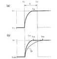
この配線遅延を簡単にモデル化したT型またはπ型モデルを図21に示す。図21(a)は、液晶装置のデータ線駆動回路に相当する電圧供給源300と、寄生抵抗R1〜R3を有するデータ線に相当するラインLと、データ線および画素の寄生容量C1〜C3とを有して構成されている。
【0005】
図21(b)は、電圧供給源300からラインLに電圧が供給されたとき、点P1〜P3の各点に接続されたそれぞれの容量C1〜C3が充電される経時変化を示している。点P1における容量C1は、電圧供給源300から距離が最も近いため、急速に充電されている。このため、所定期間t1〜t2の間の時点taで、必要電圧V1に達することができる。これに比べ、点P3における容量C3は、電圧供給源300から最も距離が遠いため、緩やかな勾配の充電特性を示す。このために、所定期間t1〜t2の間では、必要電圧V1に達することができず、時点tcにおいて、ようやく必要電圧V1に達するようになる。
【0006】
液晶装置にも上述のモデルを当てはめることができ、従来、選択された画素を所定期間内で、所定の電圧までに充電できないといった課題があった。
【0007】
本発明では、このような課題に鑑みてなされ、その目的とするところは、選択された画素を所定時間内で所定電圧まで充電することができる電気光学装置及びその駆動方法、並びに電子機器を提供することにある。
【0008】
【課題を解決するための手段】
上記課題を解決するために、本発明の一形態に係る電気光学装置は、
複数の走査線と複数のデータ線との交点に対応して形成され、電気光学物質から成る複数の画素の各々に電圧を供給して、所定の充電期間内に前記複数の画素の各々を所定の電圧まで充電する電気光学装置であって、
前記複数の走査線のうちの1つを選択する走査信号を前記複数の走査線に供給する走査線駆動手段と、
前記複数のデータ線の各々にデータ信号を供給するデータ線駆動手段と、
前記走査線駆動手段で選択される走査線と、データ信号を供給する前記データ線駆動手段との距離に基づいて、前記データ線駆動手段により供給されるデータ信号の電圧を変化させる変圧手段とを有することを特徴とする。
【0009】
このような電気光学装置およびその駆動方法によれば、選択された各画素とデータ線駆動手段との距離による充電特性に基づいて、1フレーム期間内で、走査される走査線に対応した各画素の各々に供給されるデータ信号電圧を、変圧手段により変圧できる。これにより、寄生抵抗,寄生容量などに起因して選択期間内に画素を十分に充電できないといった問題を解決できる。
【0010】
また、本発明に係る電気光学装置では、
前記変圧手段は、前記充電期間内の範囲内で前記データ線駆動手段から供給されるデータ信号を変化させる変圧期間を決定する変圧期間決定手段と、
電圧を生成する電圧生成手段と、
前記データ線駆動手段により供給されるデータ信号の電圧に、前記電圧生成手段により生成した電圧を重畳する重畳手段とを有することを特徴とする。
【0011】
このように変圧手段を構成すれば、データ線駆動手段から供給されるデータ信号電圧を、充電期間内において変圧することができる。
【0012】
また、本発明に係る電気光学装置では、
前記変圧期間決定手段は、
第1の定電流源と、
一端が前記第1の定電流源に接続され、他端が任意の電位の端子に接続された第1の容量と、
前記第1の容量と並列に接続された第1のスイッチング手段と、
前記第1の定電流源と前記第1の容量との間に、入力端子が接続された第1のバッファとを有し、
前記充電期間の終わりに同期して前記第1のスイッチング手段を閉じて前記第1の容量を放電させ、前記充電期間の始まりに同期して前記第1のスイッチング手段を開いて前記第1の容量を充電し、前記第1のバッファの論理出力に基いて前記変圧期間を決定することを特徴とする。
【0013】
このような変圧期間決定手段を用いることで、各充電期間(各選択期間)内で、もとのデータ信号電圧を変圧する変圧期間を決定できる。
【0014】
また、本発明に係る電気光学装置では、
前記変圧期間決定手段は、前記変圧期間を変更可能であることを特徴とする。
【0015】
このように選択された各画素の充電特性を変えることで、より良好な充電特性に調整することができる。
【0016】
また、本発明に係る電気光学装置では、
前記走査線駆動手段で選択された走査線と、前記データ線駆動手段との距離が近いときに比して、前記走査線駆動手段で選択された走査線と、前記データ線駆動手段との距離が遠いときには、前記変圧手段でより高い電圧に昇圧されたデータ信号が前記複数のデータ線の各々に供給されることを特徴とする。
【0017】
このように動作させると、選択された各画素とデータ線駆動手段との距離が遠くなるほど、その選択期間内の変圧期間に高い電圧を印加してやれば、寄生抵抗,寄生容量などに起因して選択期間内に画素を十分に充電できないといった問題を解決できる。
【0018】
また、本発明に係る電気光学装置では、
前記電圧生成手段は、
第2の定電流源と、
一端が前記第2の定電流源に接続され、他端が任意の電位の端子に接続された第2の容量と、
前記第2の容量と並列に接続された第2のスイッチング手段とを有し、
前記重畳手段により、前記充電期間毎に前記データ線駆動手段から供給されるデータ信号の電圧に、前記第2の容量の電圧を重畳させることを特徴とする。
【0019】
このような電圧生成手段において、第2の容量に線形的に充電される電圧を生成することができる。そして、選択された各画素とデータ線駆動手段との距離が遠くなるほど、線形的に昇圧された電圧をもとのデータ信号の電圧に重畳することで、より好ましい昇圧されたデータ信号の電圧をデータ線のそれぞれに供給することができる。
【0020】
また、本発明に係る電気光学装置では、
前記重畳手段は、前記第2の容量の電圧を任意の関数で変換する手段をさらに有することを特徴とする。
【0021】
このように、第2の容量の電圧を任意の関数により変換し、データ信号の電圧に重畳させることで、より寄生抵抗,寄生容量などに起因して選択期間内に画素を十分に充電できないといった問題を解決できる。
【0022】
また、本発明に係る電気光学装置では、
前記任意の関数は、前記データ線駆動手段から供給されるデータ信号の電圧の関数であることを特徴とする。
【0023】
この場合、もとのデータ信号の電圧に対して相対的に昇圧された電圧が重畳される。このように、任意の関数としてもとのデータ信号の電圧を用いることで、この電気光学装置において、より好ましい昇圧されたデータ信号の電圧を生成することができる。
【0024】
また、本発明に係る電気光学装置では、
前記走査線駆動手段により、1フレーム期間内の始まりから終わりまでに走査される前記複数の走査線のそれぞれをカウントするカウンタをさらに有し、
前記カウンタによりカウントされた値に基づいて、前記データ線駆動手段から供給されるデータ信号を前記変圧手段により変圧させることを特徴とする。
【0025】
こうすることで、カウンタのカウント値に基づき、その前後でデータ線駆動手段から供給されるデータ信号の電圧を変圧手段により変圧することができる。
【0026】
また、本発明に係る電気光学装置では、
1フレーム期間と対応して、その経過時間を計測する計測手段をさらに有し、
前記計測手段は、
第3の定電流源と、
一端が前記第3の定電流源に接続され、他端が任意の電位の端子に接続された第3の容量と、
前記第3の容量と並列に接続された第3のスイッチング手段と、
前記第3の定電流源と前記第3の容量との間に入力端子が接続された第2のバッファとを有し、
1フレーム期間の終わりに同期して、前記第3のスイッチング手段を閉じて前記第3の容量を放電し、1フレーム期間の始まりに同期して、前記第3のスイッチング手段を開いて前記第3の容量を充電し、このときの前記第2のバッファの論理出力に基づいて、前記データ線駆動手段から供給されるデータ信号の電圧を前記変圧手段により変化させることを特徴とする。
【0027】
このような構成とすれば、1フレーム期間内で、第3のバッファで論理出力変化する時間Tのタイミングで、変圧手段により、時間Tの前後に印加されるデータ信号の電圧を変化させることができる。
【0028】
また、本発明に係る電気光学装置では、
前記計測手段は、前記入力端子を共通の一端として並列接続された複数のバッファを有し、前記複数のバッファは論理出力の切換るタイミングの各々が異なり、
前記複数のバッファの各々の論理出力に基づいて、前記データ線駆動手段から供給されたデータ信号の電圧を前記変圧手段により変化させることを特徴とする。
【0029】
このように計測回路を構成することで、複数のバッファのそれぞれの論理出力が変化するタイミングTを複数設定できる。この複数設定されたタイミングTに基いて、変圧手段により、複数のタイミングTの前後に印加されるデータ信号の電圧を変化させることができる。
【0030】
また、本発明に係る電気光学装置では、
前記走査線駆動手段は複数個のIC(Integrated Circuit)を有し、
前記複数の走査線駆動手段IC毎に、前記データ線駆動手段から供給されるデータ信号を前記変圧手段により変圧させることを特徴とする。
【0031】
このように本発明に係る電気光学装置は、前記走査線駆動手段が複数個のIC(Integrated Circuit)から成る場合においても、前記複数の走査線駆動手段IC毎に、前記データ線駆動手段から供給されるデータ信号を前記変圧手段により変圧させることができる。
【0032】
また、本発明に係る電気光学装置では、
複数の走査線と複数のデータ線との交点に対応して形成され、電気光学物質から成る画素の各々に電圧を供給して、所定の充電期間内に前記画素を所定の電圧まで充電する電気光学装置であって、
前記複数の走査線のうちの1つを選択する走査信号を前記複数の走査線に供給する走査線駆動手段と、
前記複数のデータ線の各々の一端からデータ信号を供給する第1のデータ線駆動手段と、
前記複数のデータ線の各々の他端からデータ信号を供給する第2のデータ線駆動手段と、
前記第1のデータ線駆動手段でデータ線の各々にデータ信号が供給されるのと同期して、前記第2のデータ線駆動手段からデータ線の各々にデータ信号を供給する手段とを有することを特徴とする。
【0033】
このような電気光学装置及びその駆動方法によれば、電気光学パネルの各データ線の両端からデータ信号電圧を供給することができ、寄生抵抗,寄生容量などに起因して選択期間内に画素を十分に充電できないといった問題を解決できる。
【0034】
また、本発明に係る電気光学装置では、
複数の走査線と複数のデータ線との交点に対応して形成され、電気光学物質から成る画素の各々に電圧を供給して、所定の充電期間内に前記画素を所定の電圧まで充電する電気光学装置であって、
前記複数の走査線のうちの1つを選択する走査信号を前記複数の走査線に供給する走査線駆動手段と、
前記複数のデータ線の各々の一端からデータ信号を供給する第1のデータ線駆動手段と、
前記複数のデータ線の各々の他端からデータ信号を供給する第2のデータ線駆動手段と、
前記走査線駆動手段で選択される走査線と、データ信号を供給する前記第1のデータ線駆動手段との距離に基づいて、前記第2のデータ線駆動手段からデータ線の各々にデータ信号を供給する手段とを有することを特徴とする。
【0035】
このような電気光学装置及びその駆動方法によれば、電圧供給源である第1のデータ線駆動手段と、選択された各画素との距離が近い場合は、第1のデータ線駆動手段のみ駆動し、距離が遠くなる場合には、第2のデータ線駆動手段を併用して駆動させることができる。このようすれば、必要な時に第2のデータ線駆動手段を駆動させればよく、寄生抵抗,寄生容量などに起因して選択期間内に画素を十分に充電できないといった問題を解決できるとともに、消費電力を低減できる。
【0036】
また、本発明に係る電気光学装置では、
前記第2のデータ線駆動手段から供給されるデータ信号は、前記第1のデータ線駆動手段から供給されるデータ信号と比して階調表示精度が低く設定されていることを特徴とする。
【0037】
このように本発明に係る電気光学装置では、前記第2のデータ線駆動手段から供給されるデータ信号は、前記第1のデータ線駆動手段から供給されるデータ信号と比して階調表示精度が低く設定されていてもよい。この場合、第2のデータ線駆動手段は粗い階調表示のみを行ない、詳細な階調表示は第1のデータ線駆動手段が行なう。この第2のデータ線駆動手段のみでも、選択された画素が近ければ、急速に充電することができる。
【0038】
また、本発明に係る電気光学装置を電子機器に適用することができる。
【0039】
【発明の実施の形態】
以下、本発明の実施の形態について図面を参照して説明する。
【0040】
(第1の実施形態)
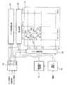
図1は、本発明の第1の実施形態に係るTFT型液晶装置のブロック図を示している。
【0041】
この液晶装置は、液晶パネル10、信号制御回路部12、階調電圧回路部14、電源回路部16、ライン駆動回路20、データ線駆動回路22および変圧回路24などから構成されている。
【0042】
ここで、液晶パネル10内に形成された画素をM(1,1)〜M(m,n)で定義する。ライン駆動回路20で駆動されるラインの総称はY、データ線駆動回路で駆動されるデータ線の総称はXで表す。このうち、ある特定のラインを指定する場合はY1、Y2、…、Yn、ある特定のデータ線を指定する場合はX1、X2、…、Xmのようにそれぞれ表記する。なお、m,nは自然数である。
【0043】
液晶パネル10は、(m×n)個(例えば、本実施形態では、m=800,n=600として説明する)の画素から構成されている。液晶パネル10内の、ある1画素M(1,1)においては、薄膜トランジスタ素子(TFT素子)30のソースにはデータ線X1が、ゲートにはラインY1がそれぞれ接続されている。データ線X1〜Xmはデータ線駆動回路22及び変圧回路24で、ラインY1〜Ynはライン駆動回路20でそれぞれ駆動される。TFT素子30のドレインには、画素電極32が設けられている。この画素電極32を一端として、容量34に蓄えられている電圧が液晶層に印加される。なお、容量34は、液晶層に印加される画素容量と、電圧を保持するための保持容量とから構成されている。また、図示しないが、通常、液晶層を介して画素電極32と対向する対向電極が設けられている。
【0044】
液晶パネル10内には、上述のような画素M(1,1)と同じ構成を有する(m×n)個の画素が形成されている。
【0045】
図1の液晶装置には、外部から電源、データ信号および同期信号が供給される。
【0046】
信号制御回路部12は、データ信号Da、クロック信号CLK1および水平同期信号Hsyncをデータ線駆動回路22に供給する。データ線駆動回路22は、例えば、各8ビットからなるRGB信号であるデータ信号Daを、クロック信号CLK1のタイミングでラッチする。この1ライン分のデータ信号Daがラッチされた後に、水平同期信号Hsyncがデータ線駆動回路22に供給される。この水平同期信号Hsyncに基づいて、ラッチされた1ライン分のデータ信号Daがアナログ信号変換され、次いで、インピーダンス変換されて、データ線Xにデータ信号電圧Vdとして供給される。
【0047】
また、信号制御回路部12は、クロック信号CLK2および垂直同期信号Vsyncをライン駆動回路20に供給する。ライン駆動回路20は、クロック信号CLK2のタイミングで、順次、選択するラインYを切換える。ある特定のラインYが選択された期間に、そのラインYに接続されたTFT素子30のゲートをオンさせる電圧Vgが印加される。このゲートがオンされるのと同期して、データ線駆動回路22から出力されたデータ信号電圧Vdが、データ線Xに供給される。液晶パネル10(画面)の全てのラインYが走査された1フレーム期間後に、垂直同期信号Vsyncがライン駆動回路20に供給されることで、再び先頭からラインYが走査される。
【0048】
電源回路部16は、階調電圧回路部14、ライン駆動回路20、データ線駆動回路22および変圧回路24などに電源を供給する。
【0049】
次に、変圧回路24について図2および図3を用いて、以下に説明する。
【0050】
図2(a)は、データ線駆動回路22の内部回路であるボルテージフォロワ142から供給されたデータ信号電圧Vdが、変圧回路24を介して、データ線Xに供給される図を示している。
【0051】
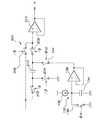
この変圧回路24は、電圧生成回路130、加算回路140およびスイッチング素子144を有して構成されている。
【0052】
加算回路140は、入力電圧の和を反転出力する回路であり、リニアな充電特性を有する容量134の電圧と、データ線駆動回路22から供給されるもとのデータ信号電圧Vdとを重畳させる。なお、この容量134の電圧が重畳される期間は、スイッチング素子144の開閉により制御される。
【0053】
電圧生成回路130は、図2(a)に示すように、定電流回路132、容量134およびスイッチング素子136などを有して構成されている。定電流回路132とスイッチング素子144とが、ボルテージフォロワ138を介して、直列に接続されている。さらに、ノードA1を一端として、容量134とスイッチング素子136とが並列に接続されている。この容量134とスイッチング素子136とは他端がともに接地されている。スイッチング素子136に供給される信号φW1は、フレーム期間毎に供給される垂直同期信号Vsyncと同期して供給される。
【0054】
この電圧生成回路130のタイミングチャートを図2(b)に示す。
【0055】
フレーム期間fに対応する信号である垂直同期信号Vsyncに基いて供給される信号φW1により、スイッチング素子136は閉じ、容量134に蓄積された電荷は放電される。この後に、スイッチング素子136は開き、容量134は波形CW1に示すように、定電流回路52により時間に比例して徐々に充電される。このように、容量134は、1フレーム期間fの間にリニアに、電圧0から電圧VW1にまで充電される充電特性を示す。
【0056】
スイッチング素子144は、例えば、Pチャネル型MOSトランジスタで構成され、その開閉は図3に示すような計測回路150によって制御される。
【0057】
計測回路150は、図3(a)に示すように、定電流回路152、容量154、スイッチング素子156およびバッファ回路158などを有して構成されている。この計測回路150では、定電流回路152とバッファ回路158は直列に接続されている。さらに、この中間点におけるノードA2を一端として、容量154とスイッチング素子156とが並列に接続されている。この容量154とスイッチング素子156とは他端がともに接地されている。スイッチング素子156に供給される信号φS1は、選択期間毎に計測回路150に供給される水平同期信号Hsyncと同期して供給される。
【0058】
この計測回路150のタイミングチャートを図3(b)に示す。
【0059】
各選択期間Hn(1≦n≦600)に対応する信号である水平同期信号Hsyncに基いて供給される信号φS1により、スイッチング素子156は閉じ、容量154に蓄積された電荷は放電される。同時に、バッファ回路158からは「L」レベルの信号φS2が出力される。この後に、スイッチング素子156は開き、容量154は波形CS1に示すように、定電流回路152により時間に比例して徐々に充電される。これと同時に、ある時点tSにおいて、バッファ回路158からは「H」レベルの信号φS2が出力される。
【0060】
したがって、図3(b)に示す選択期間H1内の期間tS1〜tSでは、スイッチング素子144がオンし、変圧回路24内の電圧生成回路130から供給された電圧は、計測回路150の制御により加算回路140に供給される。そして、昇圧されたデータ信号電圧Vaddがデータ線Xに供給される。一方、期間tS〜tS2の期間では、スイッチング素子144がオフし、電圧生成回路130で昇圧された電圧が加算回路140へ供給されず、もとのデータ信号電圧Vdがデータ線Xに供給される。
【0061】
また、図4には、このようにして、もとのデータ信号電圧Vdを昇圧したデータ信号電圧Vaddが変圧回路24によって生成されるときのタイミングチャートを示す。なお以下に示す図4〜図6において、この液晶装置は、1ドット毎に位相を反転し駆動される、ドット反転方式で駆動されている。
【0062】
図4において、昇圧されたデータ信号電圧Vaddは、各選択期間H1〜Hn内のそれぞれで出力信号φS2が「H」レベルの電圧を出力するタイミングで、容量134の電圧CW1をデータ信号電圧Vdに重畳させる形で生成される。このようにすることで、電圧供給源であるデータ線駆動回路22と、選択された各画素との距離が遠くなるに従い、データ信号電圧Vdに高い電圧を重畳させることが可能となる。
【0063】
また変形例として図5、図6には、電圧CW1レベルを適当な回路を構成し、任意の関数で変換して、もとのデータ信号電圧Vdにこの電圧CW1の変換後の電圧を重畳させたときのタイミングチャートを示す。
【0064】
図5において、昇圧されたデータ信号電圧Vaddは、上述の図4と同様な昇圧タイミングで、図2に示す容量134の電圧CW1レベルをもとに発生させたCW1×CW1に相当する電圧がさらにデータ信号電圧Vdに重畳された形で生成される。このようにすることでも、もとのデータ信号電圧Vdを昇圧する昇圧期間に、より高い電圧を重畳させることが可能となる。
【0065】
また図6において、昇圧されたデータ信号電圧Vaddは、上述の図4と同様な昇圧タイミングで、図2に示す容量134の電圧CW1に、もとのデータ信号電圧Vdレベルを対応させ重畳させた形で生成される。ここでは、CW1×Vdに相当する電圧がデータ信号電圧Vdに重畳される。このようにすることで、もとの各データ信号電圧Vdに一律に同じ電圧レベルを重畳させるのではなく、もとのデータ信号電圧Vdに対応して昇圧された電圧レベルを重畳させることが可能になる。
【0066】
また、図7および図8には、変形例として、データ線駆動回路22内に変圧回路を設けた場合の回路図を示している。
【0067】
図7の変圧回路200では、データ線Xにデータ信号電圧Vdを供給する供給線上に、スイッチング素子202〜208および容量210が設けられている。スイッチング素子202、208はクロックパルスθによって、スイッチング素子204、206はクロックパルス/θによってそれぞれ開閉が制御される。クロックパルス/θはクロックパルスθの逆論理を示す信号である。また、クロックパルスθは、前述の出力信号φS2に基づいて供給される。このような構成としても、電圧生成回路130により充電された容量210を、もとのデータ信号電圧Vdに重畳できる。
【0068】
また、図8の変圧回路220では、スイッチング素子222、224により構成されるカレントミラー回路が設けられている。前述の出力信号φS2に基づいて、スイッチング素子144がオンすることで、電圧生成回路130により生成された電圧を、もとのデータ信号電圧に重畳できる。
【0069】
なお、変圧回路24において、電圧生成回路130、計測回路150等の時定数τを変えることで、容量134および容量154の充電特性を変化させることができる。
【0070】
また、図3における計測回路150のバッファ回路158を構成するスイッチング素子のしきい値電圧Vthのそれぞれを変化させ、「H」および「L」レベルの出力のタイミングを変化させてもよい。例えば、バッファ回路158は、図18(a)に示すように、2個のインバータ回路100,101が直列に接続されている。インバータ回路100は、Nチャネル型MOSトランジスタ110とPチャネル型MOSトランジスタ111とから構成されている。インバータ回路101は、Nチャネル型MOSトランジスタ112とPチャネル型MOSトランジスタ113とから構成されている。図18(b)は例えば、インバータ100の断面図を示している。バッファ回路158がオンするまでの時間を変化させるには、例えば、インバータ100のp型ウェル104の濃度、または、n型ウェル105の濃度を変化させる。一例として、インバータ100,101のN型MOSトランジスタ110および112のどちらか一方または両方のn型拡散層104の濃度をより高くすることで、しきい値電圧を低く設定できる。これにより、バッファ回路158を速やかにオンさせることができる。したがって、変圧回路24で、もとのデータ信号電圧Vdを昇圧するための期間を短くすることができる。
【0071】
また、インバータ100を構成するNチャネル型MOSトランジスタ110,112およびPチャネル型MOSトランジスタ111,113のそれぞれのゲート長やチャネル幅などを変更することで、しきい値電圧を変化させてもよい。
【0072】
このように、時定数τおよびスイッチング素子自体の性能を変えることで、液晶パネル10を最適に動作するように調整することができるようになる。
【0073】
本実施の形態では、1フレーム期間内で、走査されるラインに対応した各画素に供給されるデータ信号電圧Vdを、変圧回路により変圧する。このとき、選択された各画素とデータ線駆動回路との距離に基いて、その選択期間内のある一定期間内に、昇圧した高い電圧をデータ線Xに供給する。これにより、寄生抵抗,寄生容量などに起因して選択期間内に画素を十分に充電できないといった問題を解決できる。
【0074】
(第2の実施形態)
図9は、第2の実施形態に係るTFT型液晶装置のブロック図を示している。
【0075】
この液晶装置は、液晶パネル10、信号制御回路部12、階調電圧回路部14、電源回路部16、ライン駆動回路20、データ線駆動回路22、変圧回路25およびカウンタ26から構成されている。
【0076】
信号制御回路部12は、水平同期信号Hsyncおよび垂直同期信号Vsyncのそれぞれをカウンタ26に供給する。このカウンタ26は、水平同期信号Hsync、つまり、1フレーム期間内で走査されたラインYの数をカウントする機能を有している。
【0077】
変圧回路25は、例えば、カウンタ26のカウント値に基づいて昇圧電圧のレベルを決定する昇圧回路と、もとのデータ信号電圧Vdに昇圧回路からの電圧を重畳させる加算回路とを有して構成されている(図示しない)。
【0078】
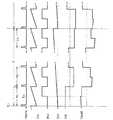
さて、図9の液晶装置の動作を、図10に示したタイミングチャートを用いて説明をする。図9の液晶パネル10は、例えば、(800×600)画素の解像度を有している。つまり、液晶パネル10は、画素M(1,1)〜画素M(800,600)を有する。
【0079】
図10では便宜的に、液晶パネル10を、画素M(1,1)〜画素M(1,199)、画素M(1,200)〜画素M(1,399)および画素M(1,400)〜画素M(1,600)の3領域に分けて説明する。図10は、この3領域に分けたうちの3つの画素、画素M(1,1)、M(1,200)およびM(1,400)のそれぞれについての充電特性の一例を示したものである。この場合、3つの画素M(1,1)、M(1,200)及びM(1,400)のそれぞれには、データ線駆動回路22から所定の電圧V1が印加されている。
【0080】
図10(a)は、ラインY1が選択され、それに対応する画素M(1,1)が充電される様子を示している。画素M(1,1)は、ラインY1が選択される選択期間t内の時点taで、所定電圧V1にまで充電されている。
【0081】
図10(b)は、選択されたラインY200に対応する画素M(1,200)が充電される様子を示している。ここで、前述の図21で説明したように、データ線駆動回路22から、充電される各画素までの距離が遠くなるほど、画素の充電特性は緩やかな勾配を描く。図10(b)に示す曲線Cbは、データ線駆動回路22から供給されるデータ信号電圧V1で、画素M(1,200)が充電される様子を示している。この場合、選択期間t内の終わりに近づく時点t2でようやく所定電圧V1に達している。しかし、図10(c)に示す曲線Ccは、データ線駆動回路22から、充電される画素までの距離がさらに遠くなるため、画素の充電特性は、より緩やかな勾配を描くことになる。このために選択期間t内では所定電圧V1に達することができない。このような充電特性を改善するために、選択期間t内に、一定期間、所定電圧よりも高い電圧を印加することで、画素を急速に充電する。
【0082】
ここで、図10(b)で画素M(1,200)が選択される場合には、このカウンタ26のカウンタ値は200を示していることになる。この際、変圧回路25はこのカウント値200に基づいて、データ線駆動回路22から供給されるデータ信号電圧V1を昇圧する。この昇圧された後のデータ信号電圧V2が、期間t1〜tb1の間に画素M(1,200)に供給される。時点tb1以降は、画素M(1,200)に供給される電圧は、もとのデータ信号電圧V1に切換り、時点tb2において、所定電圧V1で安定する。
【0083】
図10(c)では、同様に、変圧回路25で昇圧された後のデータ信号電圧V3が、期間t1〜tc1の間に画素M(1,400)に供給される。時点tc1以降は、画素M(1,400)に供給される電圧は、もとのデータ信号電圧V1に切換り、時点tc2において、所定電圧V1で安定する。
【0084】
なお、昇圧された電圧V2は、所定電圧V1よりも高く、かつ、時点tb1で電圧V1レベルに切換えたとき、選択期間t内で電圧をV1に安定させることができるように設定される。同様に、昇圧された電圧V3は、電圧V2よりも高く、かつ、時点tc1で電圧V1レベルに切換えたとき、選択期間t内で電圧をV1に安定させることができるように設定される。逆に、時点tb1,tc1は共に、選択時間t内で所定電圧V1レベルで安定させるために、時点t1から短期間の時点に設定されることが望ましい。
【0085】
ここで、図11には、本実施形態における別の実施例を示す。図11は、図10で設定したデータ信号電圧V1を昇圧する期間を変えたときの充電特性を示している。上述の3領域である、画素M(1,1)〜M(1,199)、画素M(1,200)〜M(1,399)、画素M(1,400)〜M(1,600)のそれぞれには、データ線駆動回路22からデータ信号電圧V1が供給される。
【0086】
図11(b)では、データ信号電圧Vdをt1〜tb3の期間で昇圧している。このt1〜tb3の期間は、対応する図10(b)のt1〜tb1の期間よりも短く設定されている。これにより時点tb4で所定の電圧V1に達している。図11(c)でも同様に、t1〜tc3の期間は、対応する図10(c)のt1〜tc1の期間よりも短くなっている。これにより時点tc4で所定の電圧V1に達する。
【0087】
以上、図10および図11で示したように、所定電圧V1をある電圧レベルまで昇圧させること、およびその昇圧された電圧を印加する期間を変化させることによって、所定期間t内で選択された各画素が充電されるように制御することができる。
【0088】
なお、本実施の形態では、一例として3つの領域に液晶パネル10を分け、それぞれの領域の各画素に、変圧回路25で昇圧されたデータ信号電圧Vaddを供給していた。しかし、本発明では、特にこの3つの領域に限定されるものではなく、さらに多くの領域に液晶パネルを分けて、それぞれの領域に異なる昇圧されたデータ信号電圧Vdを供給してもよい。さらに詳しくは、図9において水平同期信号Hsyncがカウンタ26に供給される毎、つまり、1本のラインが選択される毎に、画素の各々に供給されるデータ信号電圧Vdを順次、変圧回路25で昇圧してもよい。
【0089】
また、前述したのと同様に、変圧回路25内に設けられた各装置の時定数τ、スイッチング素子自体の特性を変化させることで、充電特性を変化させることができる。これにより、昇圧されたデータ信号電圧Vaddをデータ線Xのそれぞれに供給する期間を適宜、変更することができるようになる。
【0090】
このように、本実施の形態では、1フレーム期間内で、走査駆動されるラインに対応した各画素に供給されるデータ信号電圧を、変圧回路により変圧する。このとき、選択された各画素とデータ線駆動手段との距離に基いて、その選択期間内のある一定期間内に、昇圧した高い電圧をデータ線Xに供給する。これにより、寄生抵抗,寄生容量などに起因して選択期間内に画素を十分に充電できないといった問題を解決できる。
【0091】
(第3の実施形態)
図12の液晶装置は、液晶パネル10、信号制御回路部12、階調電圧回路部14、電源回路部16、ライン駆動回路20、データ線駆動回路22およびデータ線補助駆動回路40などから構成されている。ここでは例えば、各8ビットのRGB信号Daがデータ線駆動回路22に供給される。
【0092】
図12の液晶装置には、外部から電源、データ信号および同期信号が供給される。
【0093】
なお、図12のデータ線補助駆動回路40以外の装置の動作については、前述の図1の説明と同様である。
【0094】
信号制御回路部12は、クロック信号CLK1、データ信号Daおよび水平同期信号Hsyncのそれぞれの信号を、データ線補助駆動回路40に供給する。データ線補助駆動回路40には、各8ビットのRGBデータ信号Da、またはそれよりも低い階調数のRGBデータ信号Da´が供給される。本実施の形態では、このRGBデータ信号Daとして、各8ビットのRGBデータ信号Daがデータ線補助駆動回路40に供給される。
【0095】
データ線補助駆動回路40は、各8ビットからなるRGBデータ信号Daを、クロック信号CLK1のタイミングでラッチする。1ライン分のRGBデータ信号Daがラッチされるのに同期して、水平同期信号Hsyncがデータ線補助駆動回路40に供給される。この水平同期信号Hsyncに基づいて、ラッチされたRGBデータ信号Daがアナログ信号変換され、次いで、インピーダンス変換されてデータ線Xに供給される。
【0096】
階調電圧回路部14は、階調表示を行なうため、データ線駆動回路22及びデータ線補助駆動回路40のそれぞれに、同じ電圧範囲に設定された基準電圧を供給する。
【0097】
さて、図12の液晶装置には、データ線駆動回路22及びデータ線補助駆動回路40のそれぞれ2つの駆動回路が、液晶パネル10に対して、互いに対向する位置に設けられている。従来では、データ線駆動回路22のみによって液晶パネル10を駆動していた。しかし、図12に示す本実施形態の液晶装置では、電圧供給源であるデータ線駆動回路22から最も遠くにあるラインY600の方向から、データ線補助駆動回路22で、データ線Xのそれぞれにデータ信号電圧Vdを供給している。つまり、データ線駆動回路22ではデータ線Xの一端から、データ線補助駆動回路40ではデータ線Xの他端から、それぞれデータ信号電圧をデータ線Xに供給している。
【0098】
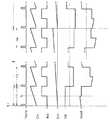
図12の液晶装置を基に、図13のタイミングチャートで動作を説明する。データ線補助駆動回路40はデータ線駆動回路22と併用して駆動されている。以下には便宜的に、液晶パネル10を2つの領域である、画素M(1,1)〜画素M(1,299)および画素(1,300)〜画素(1,600)のそれぞれに分けた場合について説明する。図13では、画素(1,1)、画素(1,300)および画素(1,600)の3つの画素それぞれについての充電特性を示している。曲線Ckは、比較のために、従来駆動での充電特性を示したものである。
【0099】
図13(a)では、電圧供給源であるデータ線駆動回路22と、選択された画素(1,1)との距離が近いため、画素(1,1)は急速に充電され、選択期間t内の時点tiで所定電圧V1に達している。
【0100】
図13(b)では、電圧供給源であるデータ線駆動回路22、およびデータ線補助駆動回路40と、選択された画素(1,300)との距離がほぼ同じである。このため、多少緩やかな勾配の充電特性を示し、選択期間t内の時点tjで所定電圧V1に達している。
【0101】
図13(c)では、電圧供給源であるデータ線補助駆動回路40と、選択された画素(1,600)との距離が近いため、画素(1,600)は急速に充電され、選択期間t内の時点tkで所定電圧V1に達している。本実施形態での各画素の充電特性は、ラインY300を基準として、ほぼ対称的な充電特性を示すことになる。
【0102】
なお、本実施形態では、データ線駆動回路22とデータ線補助駆動回路40とは同等の階調表示を行なっていたが、データ線補助駆動回路40は上述したように、データ線駆動回路22よりも低い階調表示を行なうものであってもよい。例えば、図14(a)に示すように、データ線駆動回路22の8ビットデータ信号Da(10101010)に対して、上位4ビットのデータ信号Da´(1010)のみをデータ線補助駆動回路40に供給してもよい。ただし、データ線駆動回路22およびデータ線補助駆動回路40からデータ線Xに供給される電圧振幅の範囲は、同じに設定される。図14(b)に示すように、データ線駆動回路22からデータ線Xに供給されるデータ信号電圧V11,12に対して、データ線補助駆動回路40からは、データ信号電圧V11がデータ線Xに供給される。このように、データ線補助駆動回路40で粗いデータ信号電圧をデータ線Xに供給しても、図13(c)に示した充電特性とほぼ同様に、充電特性の改善が得られる。
【0103】
このように、液晶パネルに対して対向するように設けられた2つのデータ線駆動回路を駆動させることで、寄生抵抗,寄生容量などに起因して選択期間内に画素を十分に充電できないといった問題を解決できる。
【0104】
(第4の実施形態)
図15の液晶装置は図12に示した液晶装置に、カウンタ27が設けられている。また、データ線補助駆動回路42が図12のデータ線補助駆動回路40の代わりに設けられている。このデータ線補助駆動回路42は、さらにカウンタ27から供給されるカウント値に基づいて、その駆動が制御される機能を有している。
【0105】
カウンタ27には、水平同期信号Hsyncおよび垂直同期信号Vsyncが入力される。この水平同期信号Hsyncに基いて、1フレーム期間内で走査されたラインYの数をカウントし、さらに、データ線駆動回路22およびデータ線補助駆動回路40にカウント値を供給している。カウンタ27は、1フレーム期間終了時には、垂直同期信号Vsyncでリセットされる。
【0106】
データ線駆動回路22は、例えば、各8ビットのRGBデータ信号Daが供給される。データ線補助駆動回路42には、各8ビットまたはそれよりも低い階調のRGBデータ信号Da´が供給される。本実施の形態では、このRGBデータ信号Daのうちの上位各4ビットの粗いRGBデータ信号Da´が、データ線補助駆動回路42に供給される。
【0107】
さて、図15の液晶装置には、前述の図12の液晶装置と同様に、データ線駆動回路22およびデータ線補助駆動回路42のそれぞれ2つの駆動回路が、液晶パネル10に対して、互いに対向する位置に設けられている。データ線駆動回路22ではデータ線Xの一端から、データ線補助駆動回路42ではデータ線Xの他端からそれぞれデータ信号電圧をデータ線Xに供給している。
【0108】
本実施形態では、電圧供給源であるデータ線駆動回路22と、選択された画素との距離に従って、データ線補助駆動回路42の駆動が制御される。
【0109】
この動作を、図15の液晶装置を基に、図16のタイミングチャートで説明する。なお、液晶パネル10は便宜的に2つの領域である、画素M(1,1)〜画素M(1,299)および画素(1,300)〜画素(1,600)に分けた場合について説明する。なお、曲線Chは、比較のために、従来駆動での充電特性を示したものである。
【0110】
図16(a)では、カウンタ27には、始めの水平同期信号Hsyncが入力されカウント値は1となる。このカウント値に基づいて、図15におけるデータ線駆動回路22のみが駆動されるか、または、データ線補助駆動回路42も併用して駆動されるかが決定される。本実施の形態では、カウント値1〜299では、データ線駆動回路22のみが駆動され、カウント値300〜600では、データ線補助駆動回路42もフレーム期間内のある一定期間、併用して駆動される。したがって、図16(a)では、データ線駆動回路22のみが駆動され、選択期間t内の、時点tgにおいて、所定電圧V1で安定している。
【0111】
図16(b)では、カウンタ27のカウント値は400となっている。したがって、データ線駆動回路22およびデータ線補助駆動回路42が同時に駆動されている。このデータ線補助駆動回路42は、データ線駆動回路22に供給される8ビットの各RGB信号Daの情報のうち、上位4ビットの各RGB信号Da´を供給する。前述の図14を用いて改めて説明する。このデータ線補助駆動回路42は、例えば、図14(a)に示すように、8ビットの信号データDa(10101010)のうち、上位4ビットの信号データDa´(1010)をデータ線Xのそれぞれに供給する。ここで、階調電圧回路部14から供給される基準電圧の電圧範囲は、データ線駆動回路22とデータ線補助駆動回路42とも同じである。したがって、図14(b)に示したように、データ線補助駆動回路42からは、信号データDa´(1010)に対応したデータ信号電圧V11が、データ線X1に供給される。この16階調のデータ信号電圧V11は、本来画素M(1,400)に供給すべき電圧V11,12と比べ、粗くかつ僅かに低い電圧となっている。しかし、電圧供給源であるデータ線補助駆動回路42と、画素M(1,600)との距離が近いために、データ線駆動回路22のみ駆動した場合と比べて、画素M(1,400)の充電が急速に行なわれる。図13(b)に示す本実施の形態では、期間t1〜th1までデータ線補助駆動回路42の駆動を併用することで、選択期間t内の時点th2で、画素M(1,400)を所定電圧V1にまで充電できるようになる。
【0112】
なお、本実施の形態では、一例として、ラインY300が走査された時点の前後で2つの領域に液晶パネル10を分け、一方の領域では、データ線駆動回路22のみ駆動させ、他方の領域では、データ線駆動回路22に加えてデータ線補助駆動回路42を駆動させた。しかし、本発明では、特にラインY300を境界として、データ線補助駆動回路42を駆動させるか否かを決定するように限定されるものではない。各画素の充電特性を考慮しながら、データ線補助駆動回路40を駆動するタイミングを決定するのが望ましい。
【0113】
本実施形態では、1フレーム期間内のある時点を境界として、データ線補助駆動回路42の駆動を行なうか否かを決定している。このようにすることで、常にデータ線駆動回路22と併用してデータ線補助駆動回路42を駆動させる場合と比べて、消費電力を抑えられる。
【0114】
また、例えば、本実施の形態では8ビットのデータ線駆動回路22に対して、4ビットのデータ線補助駆動回路42を用いたが、6ビットまたは2ビットなどのデータ線補助駆動回路42を用いてもよい。これに伴い、本実施形態で用いた各8ビットのRGBデータ信号Daのうち、上位各4ビットではなく、上位各6ビットまたは上位各2ビットなどのRGBデータ信号Da´がデータ線補助駆動回路42に供給される。
【0115】
さらには、本実施形態では1フレーム期間で、あるラインYが走査されるときを境界として、データ線駆動回路22とデータ線補助駆動回路42を併用して駆動させていた。しかし、上述の図16(b)に該当する領域では、選択期間t内の一定期間t1〜th1はデータ線補助駆動回路42のみを、選択期間t内の時点th1後はデータ線駆動回路22のみをそれぞれ駆動させるようにしてもよい。このようにすることでも充電特性を改善することができると同時に、消費電力の低減にもつながる。
【0116】
このように、液晶パネルに対して対向するように設けられた2つのデータ線駆動回路を駆動させることで、寄生抵抗,寄生容量などに起因して選択期間内に画素を十分に充電できないといった問題を解決できる。
【0117】
(第5の実施形態)
また、図20は、前述の図1の液晶装置の変形例として、例えば4つIC(Integrated Circuit)であるライン駆動回路20−1、20−2、20−3および20−4が直列に接続されてなる液晶装置を示している。このような場合、例えば、ライン駆動回路20−1でのラインの走査が終了すると、それを伝えるための信号であるイネーブル信号がカウンタ28に送られる。このイネーブル信号はカウンタ28によりカウントされる。このカウント値に基づいて、ライン駆動回路20−1、20−2、20−3および20−4のそれぞれで、異なるデータ信号電圧をデータ線Xに供給できるようになる。
【0118】
図示しないが、他の図12,15などの液晶装置において、ライン駆動回路22が複数のライン駆動回路から構成される場合についても同様に、イネーブル信号のカウント値に基いて、各ライン駆動回路に異なるデータ信号電圧をデータ線Xに供給できるようになる。
【0119】
(カウンタの変形例)
前述の実施形態では、カウンタ26、27、28によりデータ信号電圧Vdを昇圧するタイミングまたは、データ線補助駆動回路40、42を駆動するタイミングを決定していた。しかし、次に示すような計測回路で、前述のそれぞれのタイミングを決定してもよい。以下に図17を用いて、カウンタ26に代えて設けられた計測回路の構成と、その計測回路を有する液晶装置の動作を説明する。
【0120】
図17(a)は、計測回路170の構成を、図17(b)は、そのタイミングチャートを示した図である。
【0121】
図17(a)の計測回路170は、定電流回路172、容量174、スイッチング素子176およびバッファ回路178を有して構成されている。定電流回路172とバッファ回路178とが直列に接続されている。さらに、この中間点におけるノードA3を一端として、容量174とスイッチング素子176とが並列に接続されている。この容量174とスイッチング素子176とは他端がともに接地されている。スイッチング素子176に供給される信号φr1は、フレーム期間毎に計測回路170に供給される垂直同期信号Vsyncと同期して供給される。
【0122】
図17(b)は、この計測回路170のタイミングチャートを示している。フレーム期間毎fに対応して供給される信号である垂直同期信号Vsyncに基いて供給される信号φr1により、スイッチング素子176は閉じ、容量174に蓄積された電荷は放電されるとともに、バッファ回路178からは「L」レベルの信号φr2が出力される。この後に、スイッチング素子176は開き、容量174は波形Cr1に示すように、定電流回路172により時間に比例して徐々に充電される。これと同時に、ある時点trにおいて、バッファ回路178からは「H」レベルの信号φr2が出力される。
【0123】
前述のカウンタ26では、入力された水平同期信号Hsyncをカウントするデジタル回路で制御されていた。図17に示す計測回路170では、定電流回路172により容量174が充電されて、バッファ回路178がオンするタイミングを計測するアナログ回路で制御されている。図9において、このような計測回路170を、カウンタ26の代わりに用いることでも、電圧供給源であるデータ線駆動回路22と、充電される各画素との距離に従って、データ線Xに供給する電圧を変化させることができる。この場合、図9の液晶装置においては、tr〜tr2の期間は変圧回路25が駆動され、選択期間t内のある一定期間、昇圧されたデータ信号電圧Vdがデータ線Xに供給される。この計測回路170は、図9,15に示す液晶装置のカウンタ26、27の代わりに用いても同様に制御できる。
【0124】
カウンタ26では、カウンタ値によって、データ信号電圧Vdを昇圧するか否かを判別できた。計測回路170では、バッファ回路178がオンするまでの時間を変えることで、同様に、データ信号電圧Vdを昇圧するか否かを判別できる。
【0125】
また、この計測回路170の時定数τを変えることで、容量174の充電特性を変化させることができる。また、計測回路170のバッファ回路178を構成するスイッチング素子のしきい値電圧Vthのそれぞれを変化させ、「H」および「L」レベルの出力のタイミングを変化させてもよい。
【0126】
このように、計測回路170を用いることでも、1フレーム期間内で、容量が充電されるまでの時間Tのタイミングを適当に設定することができる。このタイミングを利用して、変圧回路25により、時間Tの前後に印加されるデータ信号の電圧を変化させることができる。
【0127】
また、図17の計測回路170では、1つのバッファ回路178を有することで、tr1〜trの期間と、tr〜tr2の期間との2つの期間に設定できたが、さらに、複数のバッファ回路を設けることで、複数の期間を設定することができる。
【0128】
図19(a)の計測回路180は、例えば、3個のバッファ回路178−1、178−2および178−3が、ノードA3を一端としてそれぞれ並列に接続されている。この3個のバッファ回路178−1、178−2および178−3の論理信号φ10〜φ12はそれぞれ、図19(b)に示すように、論理出力のタイミングが異なるように設定されている。図19(a)の場合、例えば、3つのバッファ回路178−1、178−2および178−3の論理出力のそれぞれについて、NAND回路あるいはNOR回路などを適当に組合せることで、データ信号電圧Vdにさらに電圧を重畳させるタイミングを決定することができる。
【0129】
このように計測回路180を構成することで、t1〜tm1、tm1〜tm2、tm2〜tm3およびtm3〜t2の4つの期間を設定することができる。例えば図9においては、このそれぞれの期間で、データ線駆動回路22から供給されるデータ信号電圧Vdを変圧回路25で変圧することで、選択された各画素の充電特性を改善することができるようになる。
【0130】
なお、本発明は上記実施形態に限定されるものではなく、本発明の要旨の範囲内で種々の変形実施が可能である。例えば、本発明は上述のTFT型の液晶装置の駆動に適用されるものに限らず、単純マトリックスによる画像表示装置や、2端子素子からなるTFD(Thin Film Diode)、エレクトロルミネッセンス(EL)、プラズマディスプレイ装置等を用いた画像表示装置にも適用可能である。
【0131】
本発明は、電気光学装置を備えた、例えば、携帯電話、ゲーム機器、電子手帳、パーソナルコンピュータ、ワードプロセッサ、テレビおよびカーナビゲーション装置など各種の電子機器に適用することができる。
【図面の簡単な説明】
【図1】第1の実施形態の液晶装置を示す図である。
【図2】(a)は図1の液晶装置内に設けられた変圧回路を示す図である。(b)はその変圧回路の動作を説明するためのタイミングチャートである。
【図3】(a)は図1の変圧回路内に設けられた計測回路を示す図である。(b)はその計測回路の動作を説明するためのタイミングチャートである。
【図4】図2に示す変圧回路を用いた液晶装置のタイミングチャートを示す図である。
【図5】他の形態を有する変圧回路を用いた液晶装置のタイミングチャートを示す図である。
【図6】さらに他の形態を有する変圧回路を用いた液晶装置のタイミングチャートを示す図である。
【図7】図2(a)に示す変圧回路の内部回路の変形例である。
【図8】図2(a)に示す変圧回路の内部回路の別の変形例である。
【図9】第2の実施形態の液晶装置を示す図である。
【図10】図9に示す液晶装置の画素M(1,1)、M(1,200)およびM(1,400)それぞれの充電特性を示す図である。
【図11】図9に示す液晶装置の画素M(1,1)、M(1,200)およびM(1,400)それぞれの充電特性を示す他の図である。
【図12】第3の実施形態の液晶装置を示す図である。
【図13】図12に示す液晶装置の画素M(1,1)、M(1,300)およびM(1,600)それぞれの充電特性を示す図である。
【図14】(a)は第3,4の実施形態でのデータ線補助駆動回路に供給されるデータ信号を説明するための図である。(b)は第3,4の実施形態で、データ線駆動回路およびデータ線補助駆動回路のそれぞれからデータ線Xに供給される電圧を示した図である。
【図15】第4の実施形態の液晶装置を示す図である。
【図16】図15に示す液晶装置の画素M(1,1)およびM(1,400)それぞれの充電特性を示す図である。
【図17】(a)は1フレーム期間を計測する計測回路を示す図である。(b)は計測回路の動作を説明するためのタイミングチャートである。
【図18】(a)はバッファ回路を示す図である。(b)はインバータの断面図である。
【図19】(a)は図17の計測回路に複数のバッファ回路を並列に接続した、別の計測回路を示す回路図である。(b)はこの計測回路のタイミングチャートを示す図である。
【図20】第5の実施形態の液晶装置を示す図である。
【図21】(a)はT型またはπ型モデルの回路図である。(b)は容量C1、C2およびC3のそれぞれの充電特性を示す図である。
【符号の説明】
10 液晶パネル
12 信号制御回路
14 階調電圧回路部
16 電源回路部
20,20−1,20−2,20−3,20−4 ライン駆動回路
22 データ線駆動回路
24,25 変圧回路
26,27,28 カウンタ
30 TFT素子
32 画素電極
34 画素容量および保持容量
40,42 データ線補助駆動回路
100,101 インバータ
104 n型拡散層
105 p型拡散層
110,112 Nチャネル型MOSトランジスタ
111,113 Pチャネル型MOSトランジスタ
130 電圧生成回路
132 定電流回路
134 容量
136 スイッチング素子
138 ボルテージフォロワ
140 加算回路
142 ボルテージフォロワ
144 スイッチング素子
150 計測回路
152 定電流回路
154 容量
156 スイッチング素子
158 バッファ回路
170 計測回路
172 定電流回路
174 容量
176 スイッチング素子
178,178−1,178−2,178−3,178−4 バッファ回路
180 計測回路
200 変圧回路
202,204,206,208 スイッチング素子
210 容量
212 ボルテージフォロワ
220 変圧回路
222,224 スイッチング素子
226 ボルテージフォロワ
300 電圧供給源[0001]
BACKGROUND OF THE INVENTION
The present invention relates to an electro-optical device, a driving method thereof, and an electronic apparatus.
[0002]
[Background]
For example, in an active matrix TFT (Thin Film Transistor) type liquid crystal device, RGB data is analog-converted by a data line driving circuit and supplied as a data signal voltage to a data line in the liquid crystal panel. A data signal voltage supplied to each data line from the data line driving circuit, which is also a voltage supply source, charges each pixel corresponding to the selected scanning line. At this time, particularly in a large-screen liquid crystal device, when a scanning line is selected from the side closer to the data line driving circuit within one frame period, the data line driving circuit reaches the pixel to be charged toward the end of the frame period. The distance of becomes far.
[0003]
[Problems to be solved by the invention]
In the above-described liquid crystal device, when the data signal voltage is supplied to the data line, the wiring resistance / wiring capacitance increases and the influence of the wiring delay increases especially as the liquid crystal panel has a larger screen.
[0004]
FIG. 21 shows a T-type or π-type model in which this wiring delay is simply modeled. FIG. 21A shows a
[0005]
FIG. 21B shows a point P when a voltage is supplied from the
[0006]
The above-described model can be applied to a liquid crystal device, and there has been a problem that a selected pixel cannot be charged to a predetermined voltage within a predetermined period.
[0007]
The present invention has been made in view of such problems, and an object thereof is to provide an electro-optical device capable of charging a selected pixel to a predetermined voltage within a predetermined time, a driving method thereof, and an electronic apparatus. There is to do.
[0008]
[Means for Solving the Problems]
In order to solve the above problems, an electro-optical device according to an aspect of the present invention includes:
A voltage is supplied to each of a plurality of pixels made of an electro-optical material, corresponding to the intersections of the plurality of scanning lines and the plurality of data lines, and each of the plurality of pixels is set within a predetermined charging period. An electro-optical device for charging up to a voltage of
Scanning line driving means for supplying a scanning signal for selecting one of the plurality of scanning lines to the plurality of scanning lines;
Data line driving means for supplying a data signal to each of the plurality of data lines;
Transformer for changing the voltage of the data signal supplied by the data line driver based on the distance between the scan line selected by the scan line driver and the data line driver for supplying the data signal. It is characterized by having.
[0009]
According to such an electro-optical device and its driving method, each pixel corresponding to the scanning line to be scanned within one frame period based on the charging characteristics depending on the distance between each selected pixel and the data line driving means. The data signal voltage supplied to each of these can be transformed by the transformation means. This can solve the problem that the pixel cannot be charged sufficiently within the selection period due to parasitic resistance, parasitic capacitance, and the like.
[0010]
In the electro-optical device according to the invention,
The transformation means is a transformation period determining means for determining a transformation period for changing a data signal supplied from the data line driving means within a range within the charging period;
Voltage generating means for generating a voltage;
And a superimposing unit that superimposes the voltage generated by the voltage generating unit on the voltage of the data signal supplied by the data line driving unit.
[0011]
If the transformation means is configured in this way, the data signal voltage supplied from the data line driving means can be transformed within the charging period.
[0012]
In the electro-optical device according to the invention,
The transformation period determining means includes
A first constant current source;
A first capacitor having one end connected to the first constant current source and the other end connected to a terminal of an arbitrary potential;
First switching means connected in parallel with the first capacitor;
A first buffer having an input terminal connected between the first constant current source and the first capacitor;
The first switching means is closed in synchronization with the end of the charging period.The Discharging the first capacitor and opening the first switching means in synchronization with the beginning of the charging period.And The first capacitor is charged, and the transformation period is determined based on a logic output of the first buffer.
[0013]
By using such a transformation period determining means, it is possible to determine a transformation period for transforming the original data signal voltage within each charging period (each selection period).
[0014]
In the electro-optical device according to the invention,
The transformation period determining means can change the transformation period.
[0015]
By changing the charging characteristics of each pixel selected in this way, it is possible to adjust to better charging characteristics.
[0016]
In the electro-optical device according to the invention,
The distance between the scanning line selected by the scanning line driving unit and the data line driving unit as compared to when the distance between the scanning line selected by the scanning line driving unit and the data line driving unit is short When the distance is long, the data signal boosted to a higher voltage by the transformer means is supplied to each of the plurality of data lines.
[0017]
When operated in this way, the longer the distance between each selected pixel and the data line driving means, the higher the voltage applied during the transformation period within that selection period, the selection due to parasitic resistance, parasitic capacitance, etc. The problem that the pixels cannot be charged sufficiently within the period can be solved.
[0018]
In the electro-optical device according to the invention,
The voltage generating means includes
A second constant current source;
A second capacitor having one end connected to the second constant current source and the other end connected to a terminal of an arbitrary potential;
Second switching means connected in parallel with the second capacitor;
The superimposing unit superimposes the voltage of the second capacitor on the voltage of the data signal supplied from the data line driving unit for each charging period.
[0019]
In such a voltage generation means, it is possible to generate a voltage that is linearly charged in the second capacitor. Then, as the distance between each selected pixel and the data line driving unit increases, a more preferable voltage of the boosted data signal is obtained by superimposing the linearly boosted voltage on the voltage of the original data signal. Can be supplied to each of the data lines.
[0020]
In the electro-optical device according to the invention,
The superimposing means further includes means for converting the voltage of the second capacitor by an arbitrary function.
[0021]
Thus, by converting the voltage of the second capacitor by an arbitrary function and superimposing it on the voltage of the data signal, the pixel cannot be sufficiently charged within the selection period due to parasitic resistance, parasitic capacitance, etc. Can solve the problem.
[0022]
In the electro-optical device according to the invention,
The arbitrary function is a function of a voltage of a data signal supplied from the data line driving unit.
[0023]
In this case, a relatively boosted voltage is superimposed on the original data signal voltage. As described above, by using the voltage of the original data signal as an arbitrary function, a more preferable boosted data signal voltage can be generated in the electro-optical device.
[0024]
In the electro-optical device according to the invention,
A counter that counts each of the plurality of scanning lines scanned from the beginning to the end within one frame period by the scanning line driving unit;
The data signal supplied from the data line driving unit is transformed by the transformation unit based on the value counted by the counter.
[0025]
Thus, based on the count value of the counter, the voltage of the data signal supplied from the data line driving means can be transformed by the transformation means before and after that.
[0026]
In the electro-optical device according to the invention,
Corresponding to one frame period, it further has a measuring means for measuring the elapsed time,
The measuring means includes
A third constant current source;
A third capacitor having one end connected to the third constant current source and the other end connected to a terminal of an arbitrary potential;
Third switching means connected in parallel with the third capacitor;
A second buffer having an input terminal connected between the third constant current source and the third capacitor;
In synchronization with the end of one frame period, the third switching means is closed.The The third capacitor is discharged, and the third switching means is opened in synchronization with the start of one frame period.And The third capacitor is charged, and the voltage of the data signal supplied from the data line driving unit is changed by the transforming unit based on the logic output of the second buffer at this time.
[0027]
With such a configuration, the voltage of the data signal applied before and after the time T can be changed by the transformer at the timing of the time T when the logic output changes in the third buffer within one frame period. it can.
[0028]
In the electro-optical device according to the invention,
The measuring means connects the input terminal.Common As one endA plurality of buffers connected in parallel; Each logic output switching timing is different.R ,
A voltage of a data signal supplied from the data line driving unit is changed by the transformer unit based on a logical output of each of the plurality of buffers.
[0029]
By configuring the measurement circuit in this manner, a plurality of timings T at which the respective logic outputs of the plurality of buffers change can be set. Based on the plurality of set timings T, the voltage of the data signal applied before and after the plurality of timings T can be changed by the transformer.
[0030]
In the electro-optical device according to the invention,
The scanning line driving means has a plurality of ICs (Integrated Circuits),
The data signal supplied from the data line driving means is transformed by the transformation means for each of the plurality of scanning line driving means ICs.
[0031]
As described above, in the electro-optical device according to the present invention, even when the scanning line driving unit includes a plurality of ICs (Integrated Circuits), the data line driving unit supplies each of the plurality of scanning line driving units IC. The data signal to be transmitted can be transformed by the transformation means.
[0032]
In the electro-optical device according to the invention,
Electricity is formed corresponding to the intersections of the plurality of scanning lines and the plurality of data lines, and supplies a voltage to each of the pixels made of the electro-optic material to charge the pixels to a predetermined voltage within a predetermined charging period. An optical device,
Scanning line driving means for supplying a scanning signal for selecting one of the plurality of scanning lines to the plurality of scanning lines;
First data line driving means for supplying a data signal from one end of each of the plurality of data lines;
Second data line driving means for supplying a data signal from the other end of each of the plurality of data lines;
Means for supplying a data signal to each of the data lines from the second data line driving means in synchronism with the data signal being supplied to each of the data lines by the first data line driving means; It is characterized by.
[0033]
According to such an electro-optical device and a driving method thereof, a data signal voltage can be supplied from both ends of each data line of the electro-optical panel, and pixels are selected within a selection period due to parasitic resistance, parasitic capacitance, and the like. It can solve the problem of not being able to fully charge.
[0034]
In the electro-optical device according to the invention,
Electricity is formed corresponding to the intersections of the plurality of scanning lines and the plurality of data lines, and supplies a voltage to each of the pixels made of the electro-optic material to charge the pixels to a predetermined voltage within a predetermined charging period. An optical device,
Scanning line driving means for supplying a scanning signal for selecting one of the plurality of scanning lines to the plurality of scanning lines;
First data line driving means for supplying a data signal from one end of each of the plurality of data lines;
Second data line driving means for supplying a data signal from the other end of each of the plurality of data lines;
Based on the distance between the scanning line selected by the scanning line driving means and the first data line driving means for supplying a data signal, a data signal is sent from the second data line driving means to each of the data lines. Means for supplying.
[0035]
According to the electro-optical device and the driving method thereof, when the distance between the first data line driving unit that is a voltage supply source and each selected pixel is short, only the first data line driving unit is driven. However, when the distance increases, the second data line driving means can be used in combination. In this way, the second data line driving means only needs to be driven when necessary, which can solve the problem that the pixel cannot be sufficiently charged within the selection period due to parasitic resistance, parasitic capacitance, etc. Electric power can be reduced.
[0036]
In the electro-optical device according to the invention,
The data signal supplied from the second data line driving unit has a gradation display accuracy set lower than that of the data signal supplied from the first data line driving unit.
[0037]
As described above, in the electro-optical device according to the present invention, the data signal supplied from the second data line driving unit has a gradation display accuracy higher than the data signal supplied from the first data line driving unit. May be set low. In this case, the second data line driving means performs only coarse gradation display, and the detailed gradation display is performed by the first data line driving means. Even with this second data line driving means alone, if the selected pixel is close, it can be rapidly charged.
[0038]
In addition, the electro-optical device according to the invention can be applied to an electronic apparatus.
[0039]
DETAILED DESCRIPTION OF THE INVENTION
Embodiments of the present invention will be described below with reference to the drawings.
[0040]
(First embodiment)
FIG. 1 is a block diagram of a TFT liquid crystal device according to the first embodiment of the present invention.
[0041]
The liquid crystal device includes a
[0042]
Here, the pixels formed in the
[0043]
The
[0044]
In the
[0045]
The liquid crystal device of FIG. 1 is supplied with a power supply, a data signal, and a synchronization signal from the outside.
[0046]
The signal
[0047]
Further, the signal
[0048]
The power
[0049]
Next, the
[0050]
FIG. 2A shows a diagram in which the data signal voltage Vd supplied from the voltage follower 142 which is an internal circuit of the data line driving
[0051]
The
[0052]
The
[0053]
As shown in FIG. 2A, the
[0054]
A timing chart of the
[0055]
A signal φ supplied based on a vertical synchronization signal Vsync which is a signal corresponding to the frame period fW1 As a result, the switching
[0056]
The switching
[0057]
As shown in FIG. 3A, the
[0058]
A timing chart of the
[0059]
A signal φ supplied based on a horizontal synchronization signal Hsync which is a signal corresponding to each selection period Hn (1 ≦ n ≦ 600)S1 Thus, the switching
[0060]
Therefore, the selection period H shown in FIG.1 Period tS1 ~ TS Then, the switching
[0061]
FIG. 4 shows the data signal voltage V obtained by boosting the original data signal voltage Vd in this way.add The timing chart when is generated by the
[0062]
In FIG. 4, the boosted data signal voltage Vadd Is each selection period H1 Output signal φ in each of ~ HnS2 At the timing when “H” level voltage is output, the voltage C of the
[0063]
As a modification, FIG. 5 and FIG.W1 An appropriate circuit is constructed and converted by an arbitrary function, and this voltage C is converted into the original data signal voltage Vd.W1 The timing chart when the voltage after (1) conversion is superimposed is shown.
[0064]
In FIG. 5, the boosted data signal voltage Vadd Is a voltage C C of the
[0065]
In FIG. 6, the boosted data signal voltage Vadd Is a voltage C C of the
[0066]
7 and 8 show circuit diagrams in the case where a transformer circuit is provided in the data
[0067]
In the
[0068]
Further, in the
[0069]
In the
[0070]
Further, the threshold voltage V of the switching element constituting the
[0071]
Further, the threshold voltage may be changed by changing the gate length or channel width of each of the N-
[0072]
In this way, the
[0073]
In this embodiment, the data signal voltage Vd supplied to each pixel corresponding to the scanned line is transformed by a transformer circuit within one frame period. At this time, a boosted high voltage is supplied to the data line X within a certain period within the selection period based on the distance between each selected pixel and the data line driving circuit. This can solve the problem that the pixel cannot be charged sufficiently within the selection period due to parasitic resistance, parasitic capacitance, and the like.
[0074]
(Second Embodiment)
FIG. 9 is a block diagram of a TFT liquid crystal device according to the second embodiment.
[0075]
The liquid crystal device includes a
[0076]
The signal
[0077]
The
[0078]
Now, the operation of the liquid crystal device in FIG. 9 will be described with reference to the timing chart shown in FIG. The
[0079]
In FIG. 10, for the sake of convenience, the
[0080]
FIG. 10A shows the line Y1 Is selected and the corresponding pixel M (1,1) is charged. Pixel M (1,1) is line Y1 A time t within a selection period t during which is selecteda The predetermined voltage V1 The battery is charged up to
[0081]
FIG. 10B shows the selected line Y200 A state in which the pixel M (1,200) corresponding to is charged is shown. Here, as described with reference to FIG. 21 described above, as the distance from the data line driving
[0082]
Here, when the pixel M (1,200) is selected in FIG. 10B, the counter value of the
[0083]
10C, similarly, the data signal voltage V after being boosted by the
[0084]
The boosted voltage V2 Is the predetermined voltage V1 Higher and tb1 At voltage V1 When the level is switched, the voltage is changed to V within the selection period t.1 It is set so that it can be stabilized. Similarly, the boosted voltage VThree Is the voltage V2 Higher and tc1 At voltage V1 When the level is switched, the voltage is changed to V within the selection period t.1 It is set so that it can be stabilized. Conversely, time tb1 , Tc1 Are both the predetermined voltage V within the selection time t.1 To stabilize at level t1 It is desirable to set a short time point.
[0085]
Here, FIG. 11 shows another example of the present embodiment. 11 shows the data signal voltage V set in FIG.1 The charging characteristics when the period for boosting the voltage is changed are shown. Pixels M (1,1) to M (1,199), pixels M (1,200) to M (1,399), and pixels M (1,400) to M (1,600), which are the above three regions. ) From the data line driving
[0086]
In FIG. 11B, the data signal voltage Vd is t1 ~ Tb3 The pressure is increased during the period. This t1 ~ Tb3 Is the corresponding t in FIG. 10B.1 ~ Tb1 It is set shorter than the period. As a result, time tb4 The predetermined voltage V1 Has reached. Similarly in FIG. 11C, t1 ~ Tc3 Is the corresponding t in FIG.1 ~ Tc1 It is shorter than the period. As a result, time tc4 The predetermined voltage V1 To reach.
[0087]
As described above, as shown in FIGS. 10 and 11, the predetermined voltage V1 Can be controlled such that each pixel selected within a predetermined period t is charged by raising the voltage to a certain voltage level and changing the period during which the boosted voltage is applied.
[0088]
In the present embodiment, as an example, the
[0089]
As described above, the charging characteristics can be changed by changing the time constant τ of each device provided in the
[0090]
Thus, in this embodiment, the data signal voltage supplied to each pixel corresponding to the scan-driven line is transformed by the transformer circuit within one frame period. At this time, the boosted high voltage is supplied to the data line X within a certain period within the selection period based on the distance between each selected pixel and the data line driving means. This can solve the problem that the pixel cannot be charged sufficiently within the selection period due to parasitic resistance, parasitic capacitance, and the like.
[0091]
(Third embodiment)
12 includes a
[0092]
The liquid crystal device in FIG. 12 is supplied with a power source, a data signal, and a synchronization signal from the outside.
[0093]
Note that the operations of the devices other than the data line
[0094]
The signal
[0095]
The data line
[0096]
The gradation
[0097]
In the liquid crystal device of FIG. 12, two drive circuits, the data
[0098]
The operation will be described with reference to the timing chart of FIG. 13 based on the liquid crystal device of FIG. The data line
[0099]
In FIG. 13A, since the distance between the data line driving
[0100]
In FIG. 13B, the distances between the data line driving
[0101]
In FIG. 13C, since the distance between the data line
[0102]
In the present embodiment, the data
[0103]
As described above, by driving the two data line driving circuits provided so as to face the liquid crystal panel, the pixel cannot be sufficiently charged within the selection period due to parasitic resistance, parasitic capacitance, and the like. Can be solved.
[0104]
(Fourth embodiment)
The liquid crystal device shown in FIG. 15 is provided with a
[0105]
The
[0106]
For example, the 8-bit RGB data signal Da is supplied to the data line driving
[0107]
In the liquid crystal device of FIG. 15, two drive circuits of the data
[0108]
In the present embodiment, the driving of the data line
[0109]
This operation will be described with reference to the timing chart of FIG. 16 based on the liquid crystal device of FIG. The
[0110]
In FIG. 16A, the
[0111]
In FIG. 16B, the count value of the
[0112]
In the present embodiment, as an example, the line Y300 The
[0113]
In the present embodiment, whether or not to drive the data line
[0114]
Further, for example, in the present embodiment, the 4-bit data line
[0115]
Furthermore, in the present embodiment, the data
[0116]
As described above, by driving the two data line driving circuits provided so as to face the liquid crystal panel, the pixel cannot be sufficiently charged within the selection period due to parasitic resistance, parasitic capacitance, and the like. Can be solved.
[0117]
(Fifth embodiment)
FIG. 20 shows a modification of the liquid crystal device of FIG. 1 described above. For example, four line drive circuits 20-1, 20-2, 20-3, and 20-4, which are integrated circuits (ICs), are connected in series. The liquid crystal device formed is shown. In such a case, for example, when the scanning of the line in the line driving circuit 20-1 is completed, an enable signal that is a signal for transmitting the scanning is sent to the
[0118]
Although not shown, in the other liquid crystal devices of FIGS. 12 and 15 and the like, when the
[0119]
(Counter modification)
In the above-described embodiment, the timing for boosting the data signal voltage Vd by the
[0120]
FIG. 17A shows a configuration of the
[0121]
The
[0122]
FIG. 17B shows a timing chart of the
[0123]
The
[0124]
The
[0125]
Further, by changing the time constant τ of the
[0126]
As described above, the timing of the time T until the capacitor is charged can be appropriately set within one frame period even by using the
[0127]
In addition, the
[0128]
In the
[0129]
By configuring the
[0130]
In addition, this invention is not limited to the said embodiment, A various deformation | transformation implementation is possible within the range of the summary of this invention. For example, the present invention is not limited to those applied to the driving of the above-described TFT type liquid crystal device, but is an image display device based on a simple matrix, a TFD (Thin Film Diode) composed of two terminal elements, electroluminescence (EL), plasma. The present invention can also be applied to an image display device using a display device or the like.
[0131]
The present invention can be applied to various electronic devices including an electro-optical device, such as a mobile phone, a game device, an electronic notebook, a personal computer, a word processor, a television, and a car navigation device.
[Brief description of the drawings]
FIG. 1 is a diagram illustrating a liquid crystal device according to a first embodiment.
2A is a diagram illustrating a transformer circuit provided in the liquid crystal device of FIG. 1; FIG. (B) is a timing chart for explaining the operation of the transformer circuit.
3A is a diagram showing a measurement circuit provided in the transformer circuit of FIG. 1; FIG. (B) is a timing chart for explaining the operation of the measurement circuit.
4 is a timing chart of a liquid crystal device using the transformer circuit shown in FIG. 2. FIG.
FIG. 5 is a diagram showing a timing chart of a liquid crystal device using a transformer circuit having another form.
FIG. 6 is a diagram showing a timing chart of a liquid crystal device using a transformer circuit having still another embodiment.
7 is a modified example of the internal circuit of the transformer circuit shown in FIG.
FIG. 8 is another modification of the internal circuit of the transformer circuit shown in FIG.
FIG. 9 is a diagram illustrating a liquid crystal device according to a second embodiment.
10 is a diagram showing charging characteristics of pixels M (1,1), M (1,200) and M (1,400) of the liquid crystal device shown in FIG.
11 is another diagram showing charging characteristics of the pixels M (1,1), M (1,200) and M (1,400) of the liquid crystal device shown in FIG. 9. FIG.
FIG. 12 is a diagram illustrating a liquid crystal device according to a third embodiment.
13 is a diagram showing charging characteristics of pixels M (1,1), M (1,300) and M (1,600) of the liquid crystal device shown in FIG.
FIG. 14A is a diagram for explaining a data signal supplied to a data line auxiliary drive circuit in the third and fourth embodiments; (B) is a diagram showing the voltage supplied to the data line X from each of the data line driving circuit and the data line auxiliary driving circuit in the third and fourth embodiments.
FIG. 15 is a diagram illustrating a liquid crystal device according to a fourth embodiment.
16 is a diagram showing charging characteristics of pixels M (1,1) and M (1,400) of the liquid crystal device shown in FIG.
FIG. 17A is a diagram illustrating a measurement circuit that measures one frame period. (B) is a timing chart for explaining the operation of the measurement circuit.
FIG. 18A is a diagram illustrating a buffer circuit. (B) is sectional drawing of an inverter.
FIG. 19A is a circuit diagram showing another measurement circuit in which a plurality of buffer circuits are connected in parallel to the measurement circuit of FIG. 17; (B) is a diagram showing a timing chart of the measurement circuit.
FIG. 20 is a diagram illustrating a liquid crystal device according to a fifth embodiment.
FIG. 21A is a circuit diagram of a T-type or π-type model. (B) is the capacity C1 , C2 And CThree It is a figure which shows each charge characteristic.
[Explanation of symbols]
10 LCD panel
12 Signal control circuit
14 gradation voltage circuit
16 Power supply circuit
20, 20-1, 20-2, 20-3, 20-4 Line drive circuit
22 Data line drive circuit
24, 25 Transformer circuit
26, 27, 28 counter
30 TFT element
32 pixel electrodes
34 Pixel capacity and retention capacity
40, 42 Data line auxiliary drive circuit
100, 101 inverter
104 n-type diffusion layer
105 p-type diffusion layer
110, 112 N-channel MOS transistor
111, 113 P-channel MOS transistors
130 Voltage generation circuit
132 Constant current circuit
134 capacity
136 Switching element
138 Voltage Follower
140 Adder circuit
142 Voltage Follower
144 Switching element
150 Measuring circuit
152 Constant current circuit
154 capacity
156 switching element
158 Buffer circuit
170 Measuring circuit
172 Constant current circuit
174 capacity
176 Switching element
178, 178-1, 178-2, 178-3, 178-4 Buffer circuit
180 Measuring circuit
200 Transformer circuit
202, 204, 206, 208 switching element
210 capacity
212 voltage follower
220 Transformer circuit
222,224 switching elements
226 Voltage Follower
300 Voltage supply source
Claims (9)
Translated fromJapanese前記複数の走査線のうちの1つを選択する走査信号を前記複数の走査線に順次供給する走査線駆動手段と、
前記複数のデータ線の各々にデータ信号を供給するデータ線駆動手段と、
前記走査線駆動手段で選択される走査線と、データ信号を供給する前記データ線駆動手段との距離に基づいて、前記データ線駆動手段により供給されるデータ信号の電圧を変化させる変圧手段とを有し、
前記変圧手段は、
前記充電期間内の範囲内で前記データ線駆動手段から供給されるデータ信号を変化させる変圧期間を決定する変圧期間決定手段と、
電圧を生成する電圧生成手段と、
前記データ線駆動手段により供給されるデータ信号の電圧に、前記電圧生成手段により生成した電圧を重畳する重畳手段と、
を有し、
前記電圧生成手段は、
第1の定電流源と、
一端が前記第1の定電流源に接続され、他端が任意の電位の端子に接続された第1の容量と、
前記第1の容量と並列に接続された第1のスイッチング手段と、
を有し、
前記重畳手段により、前記充電期間毎に前記データ線駆動手段から供給されるデータ信号の電圧に、前記第1の容量の電圧を重畳させ、
前記走査線駆動手段で選択された走査線と、前記データ線駆動手段との距離が近いときに比して、前記走査線駆動手段で選択された走査線と、前記データ線駆動手段との距離が遠いときには、前記変圧手段でより高い電圧に昇圧されたデータ信号が前記複数のデータ線の各々に供給されることを特徴とする電気光学装置。A voltage is supplied to each of a plurality of pixels made of an electro-optical material, corresponding to the intersections of the plurality of scanning lines and the plurality of data lines, and each of the plurality of pixels is set within a predetermined charging period. An electro-optical device for charging up to a voltage of
Scanning line driving means for sequentially supplying a scanning signal for selecting one of the plurality of scanning lines to the plurality of scanning lines;
Data line driving means for supplying a data signal to each of the plurality of data lines;
Transformer for changing the voltage of the data signal supplied by the data line driver based on the distance between the scan line selected by the scan line driver and the data line driver for supplying the data signal. Have
The transformer means is
A transformation period determining means for determining a transformation period for changing a data signal supplied from the data line driving means within a range within the charging period;
Voltage generating means for generating a voltage;
Superimposing means for superimposing the voltage generated by the voltage generating means on the voltage of the data signal supplied by the data line driving means;
Have
The voltage generating means includes
A first constant current source;
A first capacitor having one end connected to the first constant current source and the other end connected to a terminal of an arbitrary potential;
First switching means connected in parallel with the first capacitor;
Have
The superimposing unit superimposes the voltage of the first capacitor on the voltage of the data signal supplied from the data line driving unit for each charging period,
The distance between the scanning line selected by the scanning line driving unit and the data line driving unit as compared to when the distance between the scanning line selected by the scanning line driving unit and the data line driving unit is short When the distance is long, the data signal boosted to a higher voltage by the transformer means is supplied to each of the plurality of data lines.
前記変圧期間決定手段は、
第2の定電流源と、
一端が前記第2の定電流源に接続され、他端が任意の電位の端子に接続された第2の容量と、
前記第2の容量と並列に接続された第2のスイッチング手段と、
前記第2の定電流源と前記第2の容量との間に、入力端子が接続された第1のバッファとを有し、
前記充電期間の終わりに同期して前記第2のスイッチング手段を閉じて前記第2の容量を放電させ、前記充電期間の始まりに同期して前記第2のスイッチング手段を開いて前記第2の容量を充電し、前記第1のバッファの論理出力に基いて前記変圧期間を決定することを特徴とする電気光学装置。In claim 1,
The transformation period determining means includes
A second constant current source;
A second capacitor having one end connected to the second constant current source and the other end connected to a terminal of an arbitrary potential;
Second switching means connected in parallel with the second capacitor;
A first buffer having an input terminal connected between the second constant current source and the second capacitor;
The second switching means is closed in synchronization with the end of the charging period to discharge the second capacitor, and the second switching means is opened in synchronization with the beginning of the charging period to open the second capacity. And the transformation period is determined based on the logic output of the first buffer.
前記変圧期間決定手段は、前記変圧期間を変更可能であることを特徴とする電気光学装置。In claim 2,
The electro-optical device, wherein the transformation period determination means can change the transformation period.
前記重畳手段は、前記第1の容量の電圧を任意の関数で変換する手段をさらに有し、前記任意の関数は、前記データ線駆動手段から供給されるデータ信号の電圧の関数であることを特徴とする電気光学装置。In any one of Claims 1 thru | or 3,
The superimposing means further includes means for converting the voltage of the first capacitor by an arbitrary function, and the arbitrary function is a function of a voltage of a data signal supplied from the data line driving means. Electro-optical device characterized.
前記複数の走査線のうちの1つを選択する走査信号を前記複数の走査線に順次供給する走査線駆動手段と、
前記複数のデータ線の各々にデータ信号を供給するデータ線駆動手段と、
前記走査線駆動手段で選択される走査線と、データ信号を供給する前記データ線駆動手段との距離に基づいて、前記データ線駆動手段により供給されるデータ信号の電圧を変化させる変圧手段と、
1フレーム期間と対応して、その経過時間を計測する計測手段と、
を有し、
前記計測手段は、
第1の定電流源と、
一端が前記第1の定電流源に接続され、他端が任意の電位の端子に接続された第1の容量と、
前記第1の容量と並列に接続された第1のスイッチング手段と、
前記第1の定電流源と前記第1の容量との間に入力端子が接続された第1のバッファとを有し、
1フレーム期間の終わりに同期して、前記第1のスイッチング手段を閉じて前記第1の容量を放電し、1フレーム期間の始まりに同期して、前記第1のスイッチング手段を開いて前記第1の容量を充電し、このときの前記第1のバッファの論理出力に基づいて、前記データ線駆動手段から供給されるデータ信号の電圧を前記変圧手段により変化させることを特徴とする電気光学装置。A voltage is supplied to each of a plurality of pixels made of an electro-optical material, corresponding to the intersections of the plurality of scanning lines and the plurality of data lines, and each of the plurality of pixels is set within a predetermined charging period. An electro-optical device for charging up to a voltage of
Scanning line driving means for sequentially supplying a scanning signal for selecting one of the plurality of scanning lines to the plurality of scanning lines;
Data line driving means for supplying a data signal to each of the plurality of data lines;
Transforming means for changing the voltage of the data signal supplied by the data line driving means based on the distance between the scanning line selected by the scanning line driving means and the data line driving means for supplying the data signal;
Measuring means for measuring the elapsed time corresponding to one frame period;
Have
The measuring means includes
A first constant current source;
A first capacitor having one end connected to the first constant current source and the other end connected to a terminal of an arbitrary potential;
First switching means connected in parallel with the first capacitor;
A first buffer having an input terminal connected between the first constant current source and the first capacitor;
In synchronization with the end of one frame period, the first switching means is closed to discharge the first capacitor, and in synchronization with the start of one frame period, the first switching means is opened to open the first switching means. The electro-optical device is characterized in that the voltage of the data signal supplied from the data line driving means is changed by the transforming means based on the logic output of the first buffer at this time.
前記計測手段は、前記入力端子を共通の一端として並列に接続された複数のバッファを有し、前記複数のバッファは論理出力の切換るタイミングの各々が異なり、
前記複数のバッファの各々の論理出力に基づいて、前記データ線駆動手段から供給されたデータ信号の電圧を前記変圧手段により変化させることを特徴とする電気光学装置。In claim 5,
The measuring means has a plurality of buffers connected in parallel with the input terminal as a common end, and the plurality of buffers have different timings for switching logic outputs,
An electro-optical device characterized in that, based on the logic output of each of the plurality of buffers, the voltage of the data signal supplied from the data line driving unit is changed by the transforming unit.
前記走査線駆動手段は複数個のIC(Integrated Circuit)を有し、
前記複数の走査線駆動手段IC毎に、前記データ線駆動手段から供給されるデータ信号を前記変圧手段により変圧させることを特徴とする電気光学装置。In any one of Claims 1 thru | or 6.
The scanning line driving means has a plurality of ICs (Integrated Circuits),
An electro-optical device, wherein the data signal supplied from the data line driving means is transformed by the transformation means for each of the plurality of scanning line driving means ICs.
前記複数の走査線のうちの1つを選択する走査信号を前記複数の走査線に順次供給する走査線駆動手段と、
前記複数のデータ線の各々の一端からデータ信号を供給する第1のデータ線駆動手段と、
前記複数のデータ線の各々の他端からデータ信号を供給する第2のデータ線駆動手段と、
を有し、
前記複数の画素の各々に電圧を供給して、所定の充電期間内に前記画素を所定の電圧まで充電する電気光学装置の駆動方法であって、
一端が第1の定電流源に接続され、他端が任意の電位の端子に接続された第1の容量と、前記第1の容量と並列に接続された第1のスイッチング手段とを用いて、前記第1の容量に充電し、
前記第1のデータ駆動手段により前記画素を充電する前記充電期間毎に、前記第2のデータ線駆動手段から供給されるデータ信号の電圧に、前記第1の容量の電圧を重畳させ、
前記走査線駆動手段で選択された走査線と、前記第1のデータ線駆動手段との距離が近いときに比して、前記走査線駆動手段で選択された走査線と、前記第1のデータ線駆動手段との距離が遠いときには、前記第1の容量での充電電圧に基づきより高い電圧に昇圧されたデータ信号を前記第2のデータ線駆動手段から前記複数のデータ線の各々に供給することを特徴とする駆動方法。A plurality of pixels made of an electro-optic material formed corresponding to the intersections of the plurality of scanning lines and the plurality of data lines;
Scanning line driving means for sequentially supplying a scanning signal for selecting one of the plurality of scanning lines to the plurality of scanning lines;
First data line driving means for supplying a data signal from one end of each of the plurality of data lines;
Second data line driving means for supplying a data signal from the other end of each of the plurality of data lines;
Have
An electro-optical device driving method for supplying a voltage to each of the plurality of pixels and charging the pixel to a predetermined voltage within a predetermined charging period,
Using a first capacitor having one end connected to a first constant current source and the other end connected to a terminal having an arbitrary potential, and a first switching means connected in parallel to the first capacitor Charging the first capacity;
For each charging period in which the pixel is charged by the first data driving unit, the voltage of the first capacitor is superimposed on the voltage of the data signal supplied from the second data line driving unit,
The scanning line selected by the scanning line driving unit and the first data are compared with the case where the distance between the scanning line selected by the scanning line driving unit and the first data line driving unit is short. When the distance to the line driving unit is long, a data signal boosted to a higher voltage based on the charging voltage in the first capacitor is supplied from the second data line driving unit to each of the plurality of data lines. A driving method characterized by that.
Priority Applications (2)
| Application Number | Priority Date | Filing Date | Title |
|---|---|---|---|
| JP2000277811AJP3741199B2 (en) | 2000-09-13 | 2000-09-13 | ELECTRO-OPTICAL DEVICE, ITS DRIVING METHOD, AND ELECTRONIC DEVICE |
| US09/953,092US6750840B2 (en) | 2000-09-13 | 2001-09-13 | Electro-optical device, method of driving the same and electronic instrument |
Applications Claiming Priority (1)
| Application Number | Priority Date | Filing Date | Title |
|---|---|---|---|
| JP2000277811AJP3741199B2 (en) | 2000-09-13 | 2000-09-13 | ELECTRO-OPTICAL DEVICE, ITS DRIVING METHOD, AND ELECTRONIC DEVICE |
Related Child Applications (1)
| Application Number | Title | Priority Date | Filing Date |
|---|---|---|---|
| JP2005208392ADivisionJP3956980B2 (en) | 2005-07-19 | 2005-07-19 | Electro-optical device and electronic apparatus |
Publications (2)
| Publication Number | Publication Date |
|---|---|
| JP2002091364A JP2002091364A (en) | 2002-03-27 |
| JP3741199B2true JP3741199B2 (en) | 2006-02-01 |
Family
ID=18763069
Family Applications (1)
| Application Number | Title | Priority Date | Filing Date |
|---|---|---|---|
| JP2000277811AExpired - LifetimeJP3741199B2 (en) | 2000-09-13 | 2000-09-13 | ELECTRO-OPTICAL DEVICE, ITS DRIVING METHOD, AND ELECTRONIC DEVICE |
Country Status (2)
| Country | Link |
|---|---|
| US (1) | US6750840B2 (en) |
| JP (1) | JP3741199B2 (en) |
Families Citing this family (32)
| Publication number | Priority date | Publication date | Assignee | Title |
|---|---|---|---|---|
| EP1570457A2 (en)* | 2002-12-04 | 2005-09-07 | Koninklijke Philips Electronics N.V. | Active matrix pixel cell with multiple drive transistors and method for driving such a pixel |
| JP3810364B2 (en)* | 2002-12-19 | 2006-08-16 | 松下電器産業株式会社 | Display device driver |
| JP2004325808A (en)* | 2003-04-24 | 2004-11-18 | Nec Lcd Technologies Ltd | Liquid crystal display device and driving method thereof |
| JP2005196133A (en)* | 2003-12-08 | 2005-07-21 | Renesas Technology Corp | Driving circuit for display |
| JP4993847B2 (en)* | 2004-04-30 | 2012-08-08 | ルネサスエレクトロニクス株式会社 | Semiconductor integrated circuit device |
| GB0420011D0 (en)* | 2004-09-09 | 2004-10-13 | Koninkl Philips Electronics Nv | Active matrix array device and method for driving such a device |
| FR2879008A1 (en)* | 2004-12-06 | 2006-06-09 | St Microelectronics Sa | AUTOMATIC ADAPTATION OF THE POWER SUPPLY VOLTAGE OF AN ELECTROLUMINESCENT SCREEN IN ACCORDANCE WITH THE DESIRED LUMINANCE |
| FR2879007A1 (en)* | 2004-12-06 | 2006-06-09 | St Microelectronics Sa | AUTOMATIC ADAPTATION OF THE PRELOADING VOLTAGE OF AN ELECTROLUMINESCENT SCREEN |
| US8259052B2 (en) | 2005-03-07 | 2012-09-04 | Lg Display Co., Ltd. | Apparatus and method for driving liquid crystal display with a modulated data voltage for an accelerated response speed of the liquid crystal |
| KR101146531B1 (en)* | 2005-04-26 | 2012-05-25 | 삼성전자주식회사 | Display device and a driving apparatus thereof and method driving thereof |
| KR20070041845A (en)* | 2005-10-17 | 2007-04-20 | 삼성전자주식회사 | LCD, its driving device and method |
| JP2007206181A (en)* | 2006-01-31 | 2007-08-16 | Toshiba Matsushita Display Technology Co Ltd | Liquid crystal display device |
| GB2434686A (en)* | 2006-01-31 | 2007-08-01 | Sharp Kk | A drive circuit including a voltage booster |
| JP2007316380A (en)* | 2006-05-26 | 2007-12-06 | Epson Imaging Devices Corp | Electro-optical device, method for driving electro-optical device, and electronic apparatus |
| JP2008292851A (en)* | 2007-05-25 | 2008-12-04 | Nano Loa Inc | Liquid crystal device and driving method for the same |
| CN101398584B (en)* | 2007-09-27 | 2010-08-11 | 北京京东方光电科技有限公司 | Method for driving LCD device |
| KR101319350B1 (en)* | 2009-12-18 | 2013-10-16 | 엘지디스플레이 주식회사 | Liquid crystal display device |
| US9495923B2 (en) | 2011-05-18 | 2016-11-15 | Sharp Kabushiki Kaisha | Liquid crystal display device, method of driving liquid crystal display device, and television receiver |
| KR101929314B1 (en) | 2012-03-30 | 2018-12-17 | 삼성디스플레이 주식회사 | Display device |
| US10403225B2 (en)* | 2012-06-29 | 2019-09-03 | Novatek Microelectronics Corp. | Display apparatus and driving method thereof |
| WO2015083269A1 (en) | 2013-12-05 | 2015-06-11 | Necディスプレイソリューションズ株式会社 | Image display device, image display system, and image display method |
| CN103927962B (en) | 2013-12-31 | 2017-02-08 | 厦门天马微电子有限公司 | Driving circuit and method of display device |
| US9430984B2 (en) | 2014-04-15 | 2016-08-30 | Boe Technology Group Co., Ltd. | Display panel driving circuit, driving method thereof, and display device |
| KR102255575B1 (en)* | 2014-07-21 | 2021-05-26 | 삼성디스플레이 주식회사 | Display device and method of driving a display device |
| US9972235B2 (en)* | 2014-11-17 | 2018-05-15 | Panasonic Liquid Crystal Display Co., Ltd. | Liquid crystal display device including display panel and display control circuit |
| CN104537985B (en)* | 2015-01-19 | 2017-06-30 | 深圳市华星光电技术有限公司 | A kind of organic electroluminescence display panel and its voltage-drop compensation method |
| CN106297622A (en)* | 2015-06-08 | 2017-01-04 | 群创光电股份有限公司 | display device with line loss compensation function |
| JP6880594B2 (en)* | 2016-08-10 | 2021-06-02 | セイコーエプソン株式会社 | Display drivers, electro-optics and electronic devices |
| CN109427309A (en)* | 2017-08-22 | 2019-03-05 | 京东方科技集团股份有限公司 | Source drive enhances circuit, source drive Enhancement Method, source electrode drive circuit and display equipment |
| TWI797162B (en) | 2017-11-28 | 2023-04-01 | 日商索尼半導體解決方案公司 | Display device and electronic equipment |
| KR102555212B1 (en)* | 2017-12-29 | 2023-07-12 | 엘지디스플레이 주식회사 | Light emitting display device |
| TWM561222U (en)* | 2018-01-24 | 2018-06-01 | 凌巨科技股份有限公司 | A co-gate electrode between pixels structure |
Family Cites Families (6)
| Publication number | Priority date | Publication date | Assignee | Title |
|---|---|---|---|---|
| US4750813A (en)* | 1986-02-28 | 1988-06-14 | Hitachi, Ltd. | Display device comprising a delaying circuit to retard signal voltage application to part of signal electrodes |
| US5625373A (en)* | 1994-07-14 | 1997-04-29 | Honeywell Inc. | Flat panel convergence circuit |
| KR0149296B1 (en)* | 1995-08-29 | 1998-12-15 | 김광호 | Wide viewing angle driving circuit and its driving method |
| KR100188112B1 (en)* | 1996-03-15 | 1999-06-01 | 김광호 | Thin film transistor liquid crystal display |
| JPH10293561A (en)* | 1997-04-17 | 1998-11-04 | Sharp Corp | Driving method of liquid crystal display device |
| TW439000B (en)* | 1997-04-28 | 2001-06-07 | Matsushita Electric Industrial Co Ltd | Liquid crystal display device and its driving method |
- 2000
- 2000-09-13JPJP2000277811Apatent/JP3741199B2/ennot_activeExpired - Lifetime
- 2001
- 2001-09-13USUS09/953,092patent/US6750840B2/ennot_activeExpired - Lifetime
Also Published As
| Publication number | Publication date |
|---|---|
| JP2002091364A (en) | 2002-03-27 |
| US20020075219A1 (en) | 2002-06-20 |
| US6750840B2 (en) | 2004-06-15 |
Similar Documents
| Publication | Publication Date | Title |
|---|---|---|
| JP3741199B2 (en) | ELECTRO-OPTICAL DEVICE, ITS DRIVING METHOD, AND ELECTRONIC DEVICE | |
| US7683870B2 (en) | Liquid crystal display device with a pre-charging circuit | |
| CN100470630C (en) | Movable liquid crystal display and its driving method | |
| KR100583318B1 (en) | Gate driver and method of liquid crystal display | |
| CN100433100C (en) | Timing signal generating circuit for display device and display device including the same | |
| JP4584131B2 (en) | Liquid crystal display device and driving circuit thereof | |
| JP4269582B2 (en) | Liquid crystal display device, control method thereof, and portable terminal | |
| US7656382B2 (en) | Shift register and liquid crystal display device using the same | |
| CN100511399C (en) | LCD and drive circuit thereof | |
| US7692615B2 (en) | Display driver, electro-optical device, and method of driving electro-optical device | |
| JPH11119734A (en) | Drive circuit of liquid crystal display device and liquid crystal display device | |
| TWI396179B (en) | Low power driving method for a display panel and driving circuit therefor | |
| JPH1130974A (en) | Semiconductor device for drive control of liquid crystal display device and liquid crystal display device | |
| US20070262975A1 (en) | Timing generating circuit, display apparatus, and portable terminal | |
| TW200408859A (en) | Level shift circuit, display apparatus and mobile terminal | |
| JP2003173174A (en) | Image display device and display driving method | |
| KR100637060B1 (en) | Analog buffer and driving method thereof, liquid crystal display using same and driving method thereof | |
| KR20040023569A (en) | Display drive method, display element, and display | |
| CN102024399B (en) | Low-power display panel driving method and driving circuit | |
| JP3956980B2 (en) | Electro-optical device and electronic apparatus | |
| US7898516B2 (en) | Liquid crystal display device and mobile terminal | |
| CN101329848B (en) | Timing generation circuit for display apparatus and display apparatus incorporating the same | |
| JP2004198672A (en) | Display device and portable terminal | |
| JP4200709B2 (en) | Display driving method, display element, and display device | |
| JP2004191536A (en) | Display device and its driving method, and portable terminal |
Legal Events
| Date | Code | Title | Description |
|---|---|---|---|
| A977 | Report on retrieval | Free format text:JAPANESE INTERMEDIATE CODE: A971007 Effective date:20040330 | |
| A131 | Notification of reasons for refusal | Free format text:JAPANESE INTERMEDIATE CODE: A131 Effective date:20041124 | |
| A521 | Written amendment | Free format text:JAPANESE INTERMEDIATE CODE: A523 Effective date:20050105 | |
| A131 | Notification of reasons for refusal | Free format text:JAPANESE INTERMEDIATE CODE: A131 Effective date:20050517 | |
| A521 | Written amendment | Free format text:JAPANESE INTERMEDIATE CODE: A523 Effective date:20050719 | |
| TRDD | Decision of grant or rejection written | ||
| A01 | Written decision to grant a patent or to grant a registration (utility model) | Free format text:JAPANESE INTERMEDIATE CODE: A01 Effective date:20051019 | |
| A61 | First payment of annual fees (during grant procedure) | Free format text:JAPANESE INTERMEDIATE CODE: A61 Effective date:20051101 | |
| R150 | Certificate of patent or registration of utility model | Ref document number:3741199 Country of ref document:JP Free format text:JAPANESE INTERMEDIATE CODE: R150 Free format text:JAPANESE INTERMEDIATE CODE: R150 | |
| FPAY | Renewal fee payment (event date is renewal date of database) | Free format text:PAYMENT UNTIL: 20091118 Year of fee payment:4 | |
| FPAY | Renewal fee payment (event date is renewal date of database) | Free format text:PAYMENT UNTIL: 20091118 Year of fee payment:4 | |
| FPAY | Renewal fee payment (event date is renewal date of database) | Free format text:PAYMENT UNTIL: 20101118 Year of fee payment:5 | |
| FPAY | Renewal fee payment (event date is renewal date of database) | Free format text:PAYMENT UNTIL: 20101118 Year of fee payment:5 | |
| FPAY | Renewal fee payment (event date is renewal date of database) | Free format text:PAYMENT UNTIL: 20111118 Year of fee payment:6 | |
| FPAY | Renewal fee payment (event date is renewal date of database) | Free format text:PAYMENT UNTIL: 20111118 Year of fee payment:6 | |
| FPAY | Renewal fee payment (event date is renewal date of database) | Free format text:PAYMENT UNTIL: 20121118 Year of fee payment:7 | |
| FPAY | Renewal fee payment (event date is renewal date of database) | Free format text:PAYMENT UNTIL: 20121118 Year of fee payment:7 | |
| FPAY | Renewal fee payment (event date is renewal date of database) | Free format text:PAYMENT UNTIL: 20131118 Year of fee payment:8 | |
| R250 | Receipt of annual fees | Free format text:JAPANESE INTERMEDIATE CODE: R250 | |
| S111 | Request for change of ownership or part of ownership | Free format text:JAPANESE INTERMEDIATE CODE: R313113 | |
| S111 | Request for change of ownership or part of ownership | Free format text:JAPANESE INTERMEDIATE CODE: R313113 | |
| R371 | Transfer withdrawn | Free format text:JAPANESE INTERMEDIATE CODE: R371 | |
| S111 | Request for change of ownership or part of ownership | Free format text:JAPANESE INTERMEDIATE CODE: R313113 | |
| R350 | Written notification of registration of transfer | Free format text:JAPANESE INTERMEDIATE CODE: R350 | |
| R250 | Receipt of annual fees | Free format text:JAPANESE INTERMEDIATE CODE: R250 | |
| R250 | Receipt of annual fees | Free format text:JAPANESE INTERMEDIATE CODE: R250 | |
| R250 | Receipt of annual fees | Free format text:JAPANESE INTERMEDIATE CODE: R250 | |
| R250 | Receipt of annual fees | Free format text:JAPANESE INTERMEDIATE CODE: R250 | |
| EXPY | Cancellation because of completion of term |