JP3740268B2 - Electrophoretic display device - Google Patents
Electrophoretic display deviceDownload PDFInfo
- Publication number
- JP3740268B2 JP3740268B2JP01121998AJP1121998AJP3740268B2JP 3740268 B2JP3740268 B2JP 3740268B2JP 01121998 AJP01121998 AJP 01121998AJP 1121998 AJP1121998 AJP 1121998AJP 3740268 B2JP3740268 B2JP 3740268B2
- Authority
- JP
- Japan
- Prior art keywords
- electrode
- substrate
- colored
- electrophoretic particles
- display device
- Prior art date
- Legal status (The legal status is an assumption and is not a legal conclusion. Google has not performed a legal analysis and makes no representation as to the accuracy of the status listed.)
- Expired - Fee Related
Links
Images


Landscapes
- Electrochromic Elements, Electrophoresis, Or Variable Reflection Or Absorption Elements (AREA)
- Devices For Indicating Variable Information By Combining Individual Elements (AREA)
Description
Translated fromJapanese【0001】
【発明の属する技術分野】
本発明は、電気泳動粒子を移動させて表示を行う電気泳動表示装置に関する。
【0002】
【従来の技術】
近年、情報機器の発達に伴い、低消費電力且つ薄型の表示装置のニーズが増しており、これらニーズに合わせた表示装置の研究、開発が盛んに行われている。中でも、液晶表示装置は、液晶分子の配列を電気的に制御し液晶の光学的特性を変化させる事ができ、上記のニーズに対応できる表示装置として活発な開発が行われ商品化さてれいる。しかしながら、これらの液晶表示装置では、画面を見る角度や反射光による画面上の文字の見づらさや、光源のちらつき・低輝度等から生じる視覚へ負担が未だ十分に解決されていない。この為、視覚への負担の少ない表示装置の研究が盛んに検討されている。
【0003】
低消費電力、眼への負担軽減などの観点から反射型表示装置が期待されている。その1つとして、Harold D.Lees等により発明された電気泳動表示装置(米国特許USP3612758公報)が知られている。他にも、特開平9−185087号公報に電気泳動表示装置が開示されている。
【0004】
上記従来の電気泳動表示装置及びその動作原理を図8に示す。この装置85は、帯電した泳動粒子81と着色色素が溶解された絶縁性液体82からなる分散層とこの分散層を挟んで対峙する一組の電極83、84からなっている。電極83、84を介して分散層に電圧を印加することにより、泳動粒子81を粒子自身が持つ電荷と反対極性の電極に引き寄せるものである。表示はこの泳動粒子81の色と、泳動粒子81の色相と異なり着色色素が溶解された絶縁性液体82の色によって行われる。
【0005】
つまり、第1の電極83を負極に、第2の電極84を正極にした場合、正電荷の泳動粒子81が観測者に近い第1の電極83表面に移動し、第1の電極83に付着し、泳動粒子81の色が表示される(図8(b))。
【0006】
逆に、第1の電極83を正極、第2の電極84を負極した場合、正電荷の泳動粒子81が観測者から遠い第2の電極84表面に移動し、第2の電極84に付着し、絶縁性液体82内に含まれる着色色素の色が表示される(図8(a))。
【0007】
しかしながら、従来の図8の電気泳動表示装置は次のような問題点を抱えていた。第1に、絶縁性液体は着色或いは不透明化させることが不可欠であった。このため絶縁性液体は単一成分で構成することが困難であり、絶縁性液体中に何らかの着色粒子を混合したり、着色色素を溶解したりしなくてはならなかった。
【0008】
また、絶縁性液体に溶解した色素の電気泳動粒子への吸着及び電気泳動粒子が付着した電極表面と電気泳動粒子間への色素を含む絶縁性液体の侵入等の悪影響により、反射率が低下し、高いコントラストが得られない問題が生じる。
【0009】
また、このような着色粒子や着色色素の存在は、電気泳動動作において不安定要因として作用しやすく、表示装置としての性能や寿命、安定性を著しく低下させるという欠点があった。
【0010】
そこで、特開平9−211499号公報、特公平6−52358号公報、等で、着色粒子が混合されたり又は着色色素が溶解されたりしない透明な絶縁性液体を用いて表示を行う電気泳動表示装置が提案されている。
【0011】
特開平9−211499号公報で開示された電気泳動表示装置及びその動作原理を図5を用いて説明する。
【0012】
電気回路110によって、第1の電極104が電気泳動粒子108と異なった極性、第2の電極105が電気泳動粒子108と同じ極性となるように電圧を印加すると、電気泳動粒子108は、第1の電極104を被覆している誘電体層106に移動し、その表面を覆う。このとき透明基板102の外側から装置を見ている観測者は、電気泳動粒子108の色を視認する。次に、電気回路110で第1の電極104、第2の電極105にかかる電圧の極性を反転させると、電気泳動粒子108は、隠蔽層111により隠蔽された領域内の、第2の電極105を被覆している誘電体層107に移動し、その表面を覆う。電気泳動粒子108は、隠蔽層111により隠蔽された領域内にあるので、このとき観測者は誘電体層106あるいは第1の電極104あるいは第1の基板101の色すなわち電気泳動粒子108との対比色を視認する。
【0013】
【発明が解決しようとする課題】
しかしながら、従来の図11の電気泳動表示装置は次のような問題点を抱えていた。
【0014】
電気泳動粒子108を隠蔽するために、遮蔽層111を設けているので、開口率が低減し、光利用効率が低減する。よって、表示装置のコントラストも低減する。
【0015】
【課題を解決するための手段】
本発明は、上記問題点を解決するためになされたものであり、光利用効率を向上させ、コントラストの高い電気泳動表示装置を提供することを目的としている。
【0016】
この目的は以下によって達成される。
【0017】
本発明の表示装置は、第1電極と、第1電極と異なる電圧が印加される第2電極と、第1電極と第2電極の間を移動する複数の着色帯電泳動粒子と、第1基板と、第1基板と対向して配置され表面に第1基板に向かって凹状構造を持つ透明な第2基板と、前記凹状構造によって第1基板と第2基板の間に生じる空間に満たされ、該複数の着色帯電泳動粒子を保持する透明絶縁性液体と、を備えた電気泳動表示装置において、
透明絶縁性液体の屈折率は第2基板の屈折率よりも大きく、第1電極は、複数の着色帯電泳動粒子を引き付けて第1基板の中央部に集めるように配置され、第2電極は、複数の着色帯電泳動粒子を引き付けて第1基板の端部に集めるように配置され、第2基板の凹状構造は、第2基板を通って透明絶縁性液体に入射する光を第1基板の中央部に集めるような形状である、構成をとる。
【0020】
好ましくは、前記第2基板の外部表面が第1基板の中央部に光が集まるような形状である、構成をとる。
【0021】
好ましくは、前記第2基板の外部表面が第1基板に向かって凹状構造である、構成をとる。
【0022】
【発明の実施の形態】
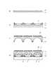
図1(a)、図1(b)に本実施形態の表示装置の断面図を示す。
【0023】
本実施形態の表示装置は、着色帯電泳動粒子4が、第1電極5と第2電極6間を水平移動することによって表示を行うものである。
【0024】
本実施形態では、第2基板2の内部表面は、第1基板1の中央部に光が集まるような形状である。よって、入射光8を集光することができるので、光利用効率を向上でき、表示コントラストを良好にする効果が得られる。
【0025】
例えば、第2基板2の内部表面が第1基板1に向かって凹状構造とする。第1基板1と第2基板2は凹状の空間を介して接合されており、その空間は透明な絶縁性液体3及び着色帯電泳動粒子4で満たされている。第1基板1には、第1電極5及び第2電極6、絶縁層7が形成されており、第1電極5は凹状空間底面の全面或いは中心部に位置し、第2電極6は凹状空間底面の周辺部に位置する。
【0026】
第2基板2の内部表面が第1基板1に向かって凹状構成に加えて、凹状空間内の光透過性の絶縁性液体3は、第2基板2を構成する材料に対して高屈折率を有する材料を使用しても良い。これによって、更に、第2基板2側からの入射光8を凹状空間内の中心部に集める集光効果を高めることができる。
【0027】
更に、絶縁層7、第1基板1などの屈折率が絶縁性液体3の屈折率よりも大きい材料を使用しても良い。更に、光利用効率を向上することができる。
【0028】
次に、着色帯電泳動粒子4の帯電のメカニズムを説明する。
【0029】
透明な絶縁性液体3中の着色泳動粒子は、着色泳動粒子と絶縁性液体の間で電荷の授受が行われ電気二重層が形成され、着色泳動粒子は正または負に帯電することが知られている。つまり、絶縁性液体から着色泳動粒子の表面に正イオン粒子又は負イオン粒子が特異吸着して、着色泳動粒子は、正電荷又は負電荷に帯電する。
【0030】
次に、本実施形態の第1の表示方法を説明する。
【0031】
絶縁性液体3中の着色帯電泳動粒子4は、第1電極5及び第2電極6に印加した電圧の極性を変えることによって、両電極上を移動させることができる。
【0032】
例えば、正に帯電した着色帯電泳動粒子4に対して、第1電極5を正極、第2電極6を負極にすれば、静電引力により、着色帯電泳動粒子4は、第2電極6上に引き付けられ、着色帯電泳動粒子4は凹状空間底面の周辺部にある第2電極6上に集まる(図1(a))。
【0033】
逆に、第1電極5を負極、第2電極6を正極にすれば、静電引力により、着色帯電泳動粒子4は、第1電極5上に引き付けられ、着色帯電泳動粒子4は凹状空間底面の中央部にある第1電極5上に集まる(図1(b))。この現象を利用することによって、表示を行うことができる。
【0034】
例えば、着色帯電泳動粒子4を中央部の第1電極5上に集めれば、凹形状の集光効果によって着色帯電泳動粒子4の色が観測側(第2基板2側)から観察される。
【0035】
逆に、凹状空間底面の周辺部にある第2電極6に集めれば、凹形状の集光効果によって絶縁層7、第1電極5、第1基板1或いは第1基板上に配置された着色層など、着色帯電泳動粒子4と光学的特性(色相、反射率、等)が異なる着色された層の色を観測側(第2基板2側)から観察することが可能となる。着色層を形成した場合、パターン化して形成しても全面に渡って形成してもよい。さらに着色層の下側に光反射層を設けてもよい。
【0036】
例えば、正電荷の着色帯電泳動粒子4を黒色にし、第1電極5を白色とすれば、白黒表示が可能となる。但し、第2基板2、絶縁層7は、透明とする。
【0037】
また、着色帯電泳動粒子4、着色帯電泳動粒子4と光学的特性(色相、反射率、等)が異なる第1電極5、絶縁層7、第1基板1の色をカラー化(例えば、イエロー、シアン、マゼンタ、等)すれば、カラー表示も可能となる。
【0038】
更に、凹形状による集光効果は、第2基板2の外部表面を第1基板1に向かって凹状に加工することによって高めることができる。図2に断面図を示す。
【0039】
更に、本実施態様では、第1電極5及び第2電極6は、第1基板1と水平な方向に重なる領域を有する。
【0040】
図1を用いて説明すると、第1電極5と第2電極6が絶縁層7を介して面で接するため、静電容量を広い面積で均一に非常に多くとることができる。つまり、キァパシター形成面積を構造的に大きく取れるので、メモリー保持力を強く維持できる効果も有する。
【0041】
次に、本実施形態の第2の表示方法を図3を用いて説明する。
【0042】
本実施形態では、着色帯電泳動粒子4を表示面に対して横方向に、面から面に水平移動させるため、構造的に表示色の階調表現が可能となる。図3において、図1で用いられている符号と同一の符号は、図1で用いられている符号と同じ部材を示す。
【0043】
階調表現は、図3に示したように着色帯電泳動粒子4を電極から他方の電極へ一部移動させることによって達成できる。例えば、パルス幅変調により階調表現をする場合、着色帯電泳動粒子4の一部を移動させる方法としては、電圧印加時間を短くする、印加電圧を小さくする、帯電能の異なる着色帯電泳動粒子4を混合して用いる、大きさの異なる着色帯電泳動粒子2を混合して用いる等がある。
【0044】
つまり、電極に印加する電圧の大きさ、電極に印加する電圧印加時間の長さ、等を調節して、移動する着色帯電泳動粒子2の移動量を制御する。つまり、第1電極8及び第2電極7を覆う着色帯電泳動粒子2の面積を制御して、面積階調を実現している。
【0045】
更に、上記構成に加えて、帯電能の異なる着色帯電泳動粒子4を混合して用いる、大きさの異なる着色帯電泳動粒子4を混合して用いることにより、階調表示の特性を向上させることができる。
【0046】
図3では、透明な絶縁性液体中3の着色帯電泳動粒子4は、正に帯電しているとする。
【0047】
第2電極6を負極に、第1電極5を正極にした場合、正電荷の着色帯電泳動粒子4が第2電極6上に移動し、正電荷の着色帯電泳動粒子4が第2電極6上に集められ、観測者(第2基板2側)からは、絶縁層7或いは第1電極5或いは第1基板1等の着色帯電泳動粒子4の色相と異なる色に着色された層の色が観察(表示)される(図3(a))。
【0048】
一方、電極に印加する電圧の極性を変え、第1電極5に印加する電圧の大きさ及び第2電極6に印加する電圧の大きさを調節して、第1電極5上に移動する正電荷の着色帯電泳動粒子4の量を制御する。
【0049】
つまり、第1電極5上を占有する着色正電荷泳動粒子4の面積を制御する。その占有面積の大きさにより、観測者(第2基板2側)からは、正電荷の着色帯電泳動粒子4の色と第2電極6の色と絶縁層7或いは第1電極5或いは第1基板1等の着色帯電泳動粒子4の色相と異なる色に着色された層の色が混合された混合色が観察される(図3(b))。例えば、着色帯電泳動粒子4を黒色にし、第1電極5を白色とすれば、白黒の階調表示が可能となる。但し、絶縁層7は、透明とする。
【0050】
本実施形態の第2の表示方法を用いると、着色帯電泳動粒子4を電極から他方の電極へ移動する量を制御できるため、面積階調表示を実現できる効果を有する。
【0051】
(別の実施形態)
また、第1電極5及び第2電極6上を絶縁層7で被覆する理由は、第1電極5及び第2電極6と絶縁性液体3との間で電気化学反応が起きてしまい、絶縁性液体3が劣化してしまうのを防止するためである。
【0052】
しかし、着色帯電泳動粒子4及び第1電極5及び第2電極6の材料を選択することにより、絶縁性液体3が劣化するのを防止することができる。よって、第2電極6を露出させて、着色帯電泳動粒子4が直接第2電極6に付着する形態をとっても良い。更に、第1電極5を露出させて、着色帯電泳動粒子4が直接第1電極5に付着する形態をとっても良い。
【0053】
また、別の本実施形態を図9を用いて説明する。図9において、図1で用いられている符号と同一の符号は、図1で用いられている符号と同じ部材を示す。第1電極5と第2電極6とが第1基板1の水平方向にのみ位置をずらして配置されている。つまり、第1電極5と第2電極6とが並設して配置され、第1基板1の水平方向に重なる領域を持たない構成とする。図9の構成をとっても、第2基板2の内部表面が第1基板1に向かって凹状構造なので、集光効果が得られ、光利用効率を高めることができる。
【0054】
(本実施形態の製造方法)
以下に、本実施態様の1例を詳細に説明する。
【0055】
図4に製造プロセスの断面図を示す。まず、第1基板1に第1電極5パターンを形成する(図4(a))。第1基板1の材料としては、耐熱性の高い材料を使用する。ポリエチレンテレフタレート(PET)、ポリエーテルサルフォン(PES)等のポリマーフィルム或いはガラス、石英等の無機材料を使用することができる。次に、第1電極5上に絶縁層7を形成し、その上に第2電極6パターンを形成する。第1電極5、絶縁層7、第2電極6に使用する材料としては、一般的に使用される絶縁材料、電極材料を使用できるが、本発明では、それらの材料色が直接表示色となるため、所望の色を表示するためには、その組み合わせを考慮する必要がある。即ち、所望の色を持った層に対して、その層よりも観察者側の層はできるだけ無色透明であることが望ましい。所望の色を持った層とは、電極材料、絶縁層、基板そのものの色であってもよく、着色材料層を各層の間或いは基板表面、裏面等に形成してもよい。また、全面に形成しても、一部に形成してもよく、複数の色を組み合わせて配置してもよい。さらに着色層に加えて観察者からみて、着色層の下側に光反射層を形成して反射率の向上を図ってもよい。電極層はスパッター蒸着等の方法により形成し、フォトリソグラフィーなどによりパターニングする。第1電極5はライン状に形成し、第2電極6も絶縁層7を介してライン状に形成する。第2電極6はライン内に円形或いは楕円形の穴を開けておく。電極ラインのピッチは通常5〜200μm程度である。
【0056】
第2電極6層上に絶縁層7を形成し、第1基板1との接合面には熱融着層9を形成しておく(図4(b))。
【0057】
次に、第2基板2を作製する。第2基板2も第1基板1と同様な材料を使用する。第2基板2の凹状の形状を形成する方法としてはどのような方法を用いてもよい。例えば、基板に熱をかけて軟化させスタンパーで形成する方法(熱プレス成形)、フォトリソグラフィでマスクを作りエッチングで形成する方法等がある。第1基板2との接合面には、熱融着層9を形成しておく(図4(c))。
【0058】
次に、絶縁性液体3及び着色帯電泳動粒子4を第2基板2の凹状の穴の中に充填する。絶縁性液体3としては、高屈折率材料ではジヨードメタン、クロルナフタリン、ブロモベンゼン、テトラブロモメタン等が使用できる。その他にも、トルエン、キシレン、シリコーンオイル、高純度石油帯が使用可能である。着色帯電泳動粒子4としては、絶縁性液体3中で帯電しうる材料を用いる。例えば、ポリエチレン、ポリスチレン等の樹脂にカーボンなどを混ぜたものを使用する。粒子の大きさとしては、通常は0.1μm〜50μm位のものを使用する。
【0059】
着色帯電泳動粒子4と絶縁性液体3を第2基板2の凹部に充填した後、第1基板1と第2の基板2を張り合わせる。張り合わせは熱による融着或いは接着剤などによって行う。これに、電圧印加手段(図示せず)を設けて表示装置が作製できる(図4(d))。
【0060】
以上の方法によって作製された表示装置は、2色表示、カラー表示、さらに階調表現が可能であり、高視野角、高コントラストを実現できる。
【0061】
【実施例】
以下に本発明を実施例を用いて説明する。
【0062】
(実施例1)
本実施例を図4を用いて説明する。厚さ150μmのPESフィルムからなる光透過性の第1基板1上にITO電極5を成膜し、フォトリソグラフィー及びウエットエッチングによりライン状にパターニングした(図4(a))。この上に絶縁層7として光を乱反射させて白色を示す酸化チタン微粒子含有樹脂層を形成した。さらに第2電極6として炭化チタンを成膜し、フォトリソグラフィー及びドライエッチングによりライン状に形成し、さらに第1電極5上にのみ円形にエッチングし穴をあけた。第2電極6上には、さらに絶縁層7として高透明ポリイミド層を形成した。次に、熱融着性接着層9を第2基板2の接合部にパターン状に形成した(図4(b))。
【0063】
PESフィルムからなる光透過性の第2基板2を熱プレス成形によって凹形状を形成し、第1基板1との接着部には第1基板1と同様に熱融着性接着層9を形成した(図4(c))。
【0064】
次に、第2基板2の凹部に、透明な絶縁性液体3及び着色帯電泳動粒子4を充填した。絶縁性液体3としては、第2基板2材料であるPESフィルムよりも屈折率が大きいジヨードメタンを使用した。着色帯電泳動粒子4としては、ポリスチレンとカーボンの混合物で、粒子の大きさが、1μm〜2μm位の黒色粒子を使用した。充填後、第1基板1及び第2基板2の接着層9の位置を合わせて、熱をかけて張り合わせた。これに電圧印加回路(図示せず)を設けて表示装置とした(図4(d))。
【0065】
次に、作製した表示装置を用いて表示を行った。印加電圧は±50Vとした。第1電極5を正極、第2電極6を負極になるように電圧を印加すると、正に帯電した着色帯電泳動粒子4は、第2基板2の凹状構造底面の周辺部にある第2電極6上に移動した。これを第2基板2側から観察すると第2基板2の凹状構造がレンズとして作用するため、第1基板1の中央部に光が集光し、露出した白色の絶縁層7に入射して、レンズ全体が白色を呈した。
【0066】
一方、極性を逆転して、第1電極5を負極、第2電極6を正極になるように電圧を印加すると、着色帯電泳動粒子4は中央部に集り、レンズ全体は着色帯電泳動粒子4の黒色を呈した。この時の応答速度は20msec以下であり、2色表示のできる表示装置を作製できた。
【0067】
(実施例2)
本実施例を図6を用いて説明する。
【0068】
実施例1と同様に、厚さ150μmのPESフィルムからなる光透過性の第1基板1上に第1電極5としてITO電極パターンを形成し(図6(a))、この上に高透明ポリイミドからなる絶縁層7を3μm形成した。さらに第2電極6としてITO電極パターン形成した。第2電極6パターンは第1電極5上のみ角の丸い長方形状にエッチングした。第2電極6上には、さらに高透明ポリイミドからなる絶縁層7を形成した(図6(b))。また、第1基板1裏側に、第2電極6のエッチング部に対応する場所にシアン、イエロー、マゼンタの着色層10を形成し、その上に光を乱反射させて白色を示す酸化チタン微粒子含有樹脂層11を形成した。第1基板1の表側には熱融着性接着層9を第2基板2とに接合部にパターン状に形成した(図6(c))。
【0069】
次に、第2基板2として、PETフィルムを熱プレス成形によって、第2基板2の内側を凹形状とし、更に、第2基板2の外側を凹形状とした。作製した第2基板2の第1基板1との接着部には、第1基板1と同様に熱融着性接着層9を形成した(図6(d))。
【0070】
次に、第1基板1の凹部に絶縁性液体3及び着色帯電泳動粒子4を充填した。絶縁性液体3にはシリコーンオイルを、着色帯電泳動粒子4にはポリスチレンとカーボンの混合物で、粒子の大きさが、1μm〜2μm位のものを使用した。充填後、第1基板1及び第2基板2の接着層9の位置を合わせて、熱をかけて張り合わせた。これに電圧印加回路(図示せず)を設けて表示装置とした(図6(e))。
【0071】
次に、作製した表示装置を用いて表示を行った。印加電圧を±50V、電圧印加時間を20msecとした。第1電極5を正極、第2電極6を負極になるように電圧を印加すると、正に帯電した着色帯電泳動粒子4は、第2基板2の凹状構造底面の周辺部にある第2電極6上に移動した。これを第2基板2側から観察すると第2基板2の凹状構造がレンズとして作用するため、レンズ全体が着色層10の色を呈した。
【0072】
一方、極性を逆転して、第1電極5を負極、第2電極6を正極になるように電圧を印加すると、着色帯電泳動粒子4は中央部に集り、レンズ全体は着色帯電泳動粒子4の黒色を呈した。応答速度は20msec以下であり、良好にカラー表示を行うことができた。
【0073】
次に、印加電圧を±50V、電圧印加時間を5msecにして駆動したところ、各着色層からの反射光の明るを半分程度に低下させることができた。電圧印加時間を種々選択することで、多段階の階調表現を行うことが可能であった。以上により、階調表現可能なカラー表示装置を作製できた。
【0074】
(実施例3)
本実施例を図7を用いて説明する。実施例1と同様に、厚さ150μmのPESフィルムからなる光透過性の第1基板1上に第1電極5としてITO電極パターンを形成した(図7(a))。この上に高透明ポリイミドからなる絶縁層7を3μm形成した。さらに第2電極6として炭化チタンを成膜し、フォトリソグラフィー及びドライエッチングによりライン状に形成し、さらに第1電極5上にのみ円形にエッチングし穴をあけた。第2電極6上には、さらに絶縁層7として高透明ポリイミド層を形成した(図7(b))。また、第1基板1裏側には光を乱反射させて白色を示す酸化チタン微粒子含有樹脂層11を全面に形成した。第1基板1の表側には熱融着性接着層9を第2基板2とに接合部にパターン状に形成した。
【0075】
次に、第2基板2を熱プレス成形によって凹形状を形成し、非加工面の凹部に対応する場所にシアン、イエロー、マゼンタの各着色フィルター層12を形成した。その上に透明保護層12を形成した。作製した第2基板2の凹形状側の第1基板1との接着部には第1基板と同様に熱融着性接着層9を形成した(図7(c))。
【0076】
次に、第2基板2の凹部に絶縁性液体3及び着色帯電泳動粒子4を充填した。絶縁性液体3にはシリコーンオイルを、着色帯電泳動粒子4にはポリスチレンとカーボンの混合物で、粒子の大きさが、1μm〜2μm位のものを使用した。充填後、第1基板1及び第2基板2の接着層9の位置を合わせて、熱をかけて張り合わせた。これに電圧印加回路(図示せず)を設けて表示装置とした(図7(d))。
【0077】
次に、作製した表示装置を用いて表示を行った。印加電圧を±50V、電圧印加時間を20msecとした。第1電極5を正極、第2電極6を負極になるように電圧を印加すると、正に帯電した着色帯電泳動粒子4は、第2基板2の凹状構造底面の周辺部にある第2電極6上に移動した。これを第2基板2側から観察すると第2基板2の凹状構造がレンズとして作用するため、レンズ全体が着色フィルター層12の色を呈した。
【0078】
一方、極性を逆転して、第1電極5を負極、第2電極6を正極になるように電圧を印加すると、着色帯電泳動粒子4は中央部に集り、レンズ全体は着色帯電泳動粒子4の黒色を呈した。応答速度は20msec以下であり、良好にカラー表示を行うことができた。
【0079】
次に、印加電圧を±50V、電圧印加時間を5msecにして駆動したところ、各着色層からの反射光の明るを半分程度に低下させることができた。電圧印加時間を種々選択することで、多段階の階調表現を行うことが可能であった。以上により、階調表現可能なカラー表示装置を作製できた。
【0080】
(実施例4)
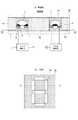
図10は、実施例1を利用した表示装置の1例の概略構成を示すものである。図10(a)は、本実施例の表示装置82の断面図(図10(b)の破線A−A' に沿う断面図)で、図10(b)は、その平面図である。
【0081】
PETフィルムからなる第1基板1の表面の全面に灰色の顔料層を形成した。
【0082】
その後、実施例1と同様に第1電極5、絶縁層7、第2電極6、着色帯電泳動粒子4、絶縁性液体3、凹状構造の第2基板2を有するセル83を形成した。
【0083】
その後、第1基板1の表面に隔壁81を図10(b)のように形成した。
【0084】
その後、パルス発生器84を第2電極6に接続して、表示装置82とした。また、第1電極5は、アース接地する。セル83の形状・サイズは、所望の解像度に合わせて選択する必要があるが、本実施例では、簡単にするため、7つのセル83が8の字形状に配置された7セグメント・タイプを用いた。
【0085】
作製した表示装置82を用いて表示を行った。全第2電極5に、波高値マイナス50V、パルス幅10msの矩形波を印加した。本実施例で用いた着色帯電泳動粒子4は、ジヨードメタン中で正に帯電していたため、電圧印加により負電圧マイナス50Vが印加された黒色の第2電極6上に移動した。これにより、第2基板5(観測側)から見た全セル83内を灰色がかった白色状態とした。一方、第2電極6のうち、任意のものをスイッチ(図示せず)で選択した上で、第2電極6に逆極性のパルス、波高値プラス50V、パルス幅10msの矩形波を印加したところ、白色の絶縁層7上に着色帯電泳動粒子4が移動するため、選択されたセル83内は,黒色状態となり、セグメント形状の組み合わせを利用した表示(0〜9までの数字表示やアルファベットの一部表示)が可能であることを確認した。応答速度は20msec以下であった。
【0086】
例えば、全部の第2電極6をスイッチで選択して、第2電極6に逆極性のパルス、波高値プラス50V、パルス幅10msの矩形波を印加した場合、全セル83内は,黒色状態となり、黒色で数字の8を表示できる。
【0087】
【発明の効果】
以上、詳細に述べたように、本発明は次のような作用効果を持つ。
・ レンズ構造を有するため泳動粒子を表示面の横方向に移動させる表示方法であっても高いコントラストの表示ができる。
・ レンズ内で泳動粒子を駆動させるため、レンズ構造を基板上に積層する場合と比べて装置を薄膜化できる。
・ 構造が極めて簡単なため、大画面表示装置化は極めて容易にできる。
【図面の簡単な説明】
【図1】本発明の表示装置の断面図を示す。
【図2】本発明の他の表示装置の断面図を示す。
【図3】本発明の表示装置の階調表現方法の図を示す。
【図4】本発明の表示装置の製造方法の一例の図を示す。
【図5】従来の電気泳動型表示装置の原理の図を示す。
【図6】本発明の表示装置の製造方法の一例の図を示す。
【図7】本発明の表示装置の製造方法の一例の図を示す。
【図8】従来の電気泳動型表示装置の原理の図を示す。
【図9】本発明の他の表示装置の断面図を示す。
【図10】本実施例4に用いられる表示装置の断面図を示す。
【符号の説明】
1 第1基板
2 第2基板
3 絶縁性液体
4 着色帯電泳動粒子
5 第1電極
6 第2電極
7 絶縁層
8 入射光
9 熱融着層
10 着色層
11 光反射層
12 着色フィルター層
81 隔壁
82 表示装置
83 セル
84 パルス発生器[0001]
BACKGROUND OF THE INVENTION
The present invention relates to an electrophoretic display device that performs display by moving electrophoretic particles.
[0002]
[Prior art]
In recent years, with the development of information equipment, the need for low power consumption and thin display devices is increasing, and research and development of display devices that meet these needs are being actively conducted. Above all, liquid crystal display devices can change the optical characteristics of liquid crystals by electrically controlling the arrangement of liquid crystal molecules, and are actively developed and commercialized as display devices that can meet the above needs. However, in these liquid crystal display devices, the visual burden caused by the angle at which the screen is viewed, the difficulty in seeing characters on the screen due to reflected light, the flickering of the light source, low luminance, etc. has not been sufficiently solved. For this reason, research on display devices with less visual burden has been actively studied.
[0003]
Reflective display devices are expected from the viewpoints of low power consumption and reduced burden on the eyes. For example, Harold D. An electrophoretic display device invented by Lees et al. (US Pat. No. USP3612758) is known. In addition, an electrophoretic display device is disclosed in Japanese Patent Laid-Open No. 9-185087.
[0004]
FIG. 8 shows the conventional electrophoretic display device and its operating principle. The
[0005]
That is, when the
[0006]
Conversely, when the
[0007]
However, the conventional electrophoretic display device of FIG. 8 has the following problems. First, it was essential that the insulating liquid be colored or opaque. For this reason, it is difficult to constitute the insulating liquid with a single component, and it has been necessary to mix some colored particles in the insulating liquid or dissolve the coloring pigment.
[0008]
In addition, the reflectance decreases due to adverse effects such as adsorption of the dye dissolved in the insulating liquid onto the electrophoretic particles and penetration of the insulating liquid containing the dye between the electrode surface on which the electrophoretic particles adhere and the electrophoretic particles. This causes a problem that high contrast cannot be obtained.
[0009]
Further, the presence of such colored particles and coloring pigments tends to act as an unstable factor in the electrophoresis operation, and has a drawback that the performance, life and stability as a display device are remarkably lowered.
[0010]
In view of this, an electrophoretic display device that performs display using a transparent insulating liquid in which colored particles are not mixed or colored pigments are not dissolved is disclosed in Japanese Patent Application Laid-Open No. 9-2111499, Japanese Patent Publication No. 6-52358, and the like. Has been proposed.
[0011]
An electrophoretic display device disclosed in Japanese Patent Laid-Open No. 9-2111499 and its operating principle will be described with reference to FIG.
[0012]
When a voltage is applied by the
[0013]
[Problems to be solved by the invention]
However, the conventional electrophoretic display device of FIG. 11 has the following problems.
[0014]
Since the
[0015]
[Means for Solving the Problems]
SUMMARY An advantage of some aspects of the invention is to provide an electrophoretic display device with improved light utilization efficiency and high contrast.
[0016]
This objective is achieved by:
[0017]
The display device of the present invention includes a first electrode, a second electrode to which a voltage different from the first electrode is applied, a plurality of colored charged electrophoretic particles moving between the first electrode and the second electrode, and a first substrate. And arranged to face the first substrateTransparent with concave structure on the surface toward the first substrate A second substrate;By the concave structure Between the first board and the second boardSpace that occurs in MetThe In an electrophoretic display device comprising a transparent insulating liquid that holds a plurality of colored charged electrophoretic particles,
The refractive index of the transparent insulating liquid is larger than the refractive index of the second substrate, The first electrode isAttract multiple colored electrophoretic particles In the center of the first boardTo collect And the second electrode isAttract multiple colored electrophoretic particles At the end of the first substrateTo collect Of the second substrateConcave structure IsLight incident on the transparent insulating liquid through the second substrate In the center of the first boardGather The configuration is such a shape.
[0020]
Preferably, the outer surface of the second substrate is configured to collect light at the center of the first substrate.
[0021]
Preferably, the outer surface of the second substrate has a concave structure toward the first substrate.
[0022]
DETAILED DESCRIPTION OF THE INVENTION
1A and 1B are cross-sectional views of the display device of this embodiment.
[0023]
In the display device of this embodiment, the colored charged electrophoretic particles 4 perform display by moving horizontally between the
[0024]
In the present embodiment, the inner surface of the
[0025]
For example, the inner surface of the
[0026]
In addition to the concave configuration of the inner surface of the
[0027]
Furthermore, a material having a higher refractive index than that of the insulating
[0028]
Next, the charging mechanism of the colored charged electrophoretic particles 4 will be described.
[0029]
It is known that the colored electrophoretic particles in the transparent insulating
[0030]
Next, the first display method of this embodiment will be described.
[0031]
The colored electrophoretic particles 4 in the insulating
[0032]
For example, if the
[0033]
On the contrary, if the
[0034]
For example, when the colored charged electrophoretic particles 4 are collected on the
[0035]
On the contrary, if it collects on the
[0036]
For example, when the positively charged colored electrophoretic particles 4 are black and the
[0037]
In addition, the colored charged electrophoretic particles 4 and the colors of the
[0038]
Further, the condensing effect due to the concave shape can be enhanced by processing the outer surface of the
[0039]
Further, in the present embodiment, the
[0040]
Referring to FIG. 1, since the
[0041]
Next, the second display method of this embodiment will be described with reference to FIG.
[0042]
In the present embodiment, since the colored charged electrophoretic particles 4 are moved horizontally from side to side in the horizontal direction with respect to the display surface, the gradation of the display color can be structurally expressed. 3, the same reference numerals as those used in FIG. 1 denote the same members as those used in FIG.
[0043]
The gradation expression can be achieved by partially moving the colored charged electrophoretic particles 4 from one electrode to the other electrode as shown in FIG. For example, when gradation representation is performed by pulse width modulation, a part of the colored charged electrophoretic particles 4 can be moved by shortening the voltage application time, reducing the applied voltage, or colored charged electrophoretic particles 4 having different charging capabilities. Are mixed and used, and colored charged
[0044]
That is, the moving amount of the colored charged
[0045]
Furthermore, in addition to the above-described configuration, the colored display electrophoretic particles 4 having different charging capabilities are mixed and used, and the colored display electrophoretic particles 4 having different sizes can be mixed to improve the gradation display characteristics. it can.
[0046]
In FIG. 3, it is assumed that the colored charged electrophoretic particles 4 in the transparent insulating
[0047]
When the
[0048]
On the other hand, by changing the polarity of the voltage applied to the electrode and adjusting the magnitude of the voltage applied to the
[0049]
That is, the area of the colored positively charged electrophoretic particles 4 occupying the
[0050]
When the second display method of the present embodiment is used, the amount of movement of the colored charged electrophoretic particles 4 from the electrode to the other electrode can be controlled, so that an area gradation display can be realized.
[0051]
(Another embodiment)
The reason for covering the
[0052]
However, it is possible to prevent the insulating
[0053]
Another embodiment will be described with reference to FIG. 9, the same reference numerals as those used in FIG. 1 denote the same members as those used in FIG. The
[0054]
(Manufacturing method of this embodiment)
Hereinafter, an example of this embodiment will be described in detail.
[0055]
FIG. 4 shows a sectional view of the manufacturing process. First, the
[0056]
An insulating
[0057]
Next, the
[0058]
Next, the insulating
[0059]
After the colored charged electrophoretic particles 4 and the insulating
[0060]
The display device manufactured by the above method can perform two-color display, color display, and gradation expression, and can realize a high viewing angle and a high contrast.
[0061]
【Example】
The present invention will be described below with reference to examples.
[0062]
Example 1
This embodiment will be described with reference to FIG. An
[0063]
A concave shape was formed on the light-transmitting
[0064]
Next, the concave portion of the
[0065]
Next, display was performed using the manufactured display device. The applied voltage was ± 50V. When a voltage is applied so that the
[0066]
On the other hand, when the polarity is reversed so that the voltage is applied so that the
[0067]
(Example 2)
This embodiment will be described with reference to FIG.
[0068]
As in Example 1, an ITO electrode pattern was formed as a
[0069]
Next, as the
[0070]
Next, the concave portion of the
[0071]
Next, display was performed using the manufactured display device. The applied voltage was ± 50 V, and the voltage application time was 20 msec. When a voltage is applied so that the
[0072]
On the other hand, when the polarity is reversed so that the voltage is applied so that the
[0073]
Next, when it was driven with an applied voltage of ± 50 V and a voltage application time of 5 msec, the brightness of reflected light from each colored layer could be reduced to about half. Multi-level gradation expression can be performed by variously selecting the voltage application time. As described above, a color display device capable of expressing gradation can be manufactured.
[0074]
Example 3
This embodiment will be described with reference to FIG. As in Example 1, an ITO electrode pattern was formed as the
[0075]
Next, a concave shape was formed on the
[0076]
Next, the concave portion of the
[0077]
Next, display was performed using the manufactured display device. The applied voltage was ± 50 V, and the voltage application time was 20 msec. When a voltage is applied so that the
[0078]
On the other hand, when the polarity is reversed so that the voltage is applied so that the
[0079]
Next, when it was driven with an applied voltage of ± 50 V and a voltage application time of 5 msec, the brightness of reflected light from each colored layer could be reduced to about half. Multi-level gradation expression can be performed by variously selecting the voltage application time. As described above, a color display device capable of expressing gradation can be manufactured.
[0080]
(Example 4)
FIG. 10 shows a schematic configuration of an example of a display device using the first embodiment. FIG. 10A is a cross-sectional view (a cross-sectional view taken along the broken line AA ′ in FIG. 10B) of the
[0081]
A gray pigment layer was formed on the entire surface of the
[0082]
Thereafter, as in Example 1, a
[0083]
Thereafter, a
[0084]
Thereafter, the
[0085]
Display was performed using the manufactured
[0086]
For example, when all the
[0087]
【The invention's effect】
As described above in detail, the present invention has the following effects.
-Since it has a lens structure, high contrast display is possible even with a display method in which migrating particles are moved in the horizontal direction of the display surface.
-Since the migrating particles are driven in the lens, the apparatus can be made thinner than when the lens structure is laminated on the substrate.
・ Since the structure is extremely simple, it is extremely easy to make a large screen display device.
[Brief description of the drawings]
FIG. 1 is a cross-sectional view of a display device of the present invention.
FIG. 2 is a cross-sectional view of another display device of the present invention.
FIG. 3 shows a diagram of a gray scale expression method for a display device of the present invention.
FIG. 4 shows an example of a method for manufacturing a display device of the present invention.
FIG. 5 is a diagram illustrating the principle of a conventional electrophoretic display device.
FIG. 6 shows an example of a method for manufacturing a display device of the present invention.
FIG. 7 shows an example of a method for manufacturing a display device of the present invention.
FIG. 8 is a diagram illustrating the principle of a conventional electrophoretic display device.
FIG. 9 is a cross-sectional view of another display device of the present invention.
10 shows a cross-sectional view of a display device used in Example 4. FIG.
[Explanation of symbols]
1 First substrate
2 Second substrate
3 Insulating liquid
4 Colored electrophoretic particles
5 First electrode
6 Second electrode
7 Insulation layer
8 Incident light
9 Heat-fusion layer
10 Colored layer
11 Light reflection layer
12 Colored filter layer
81 Bulkhead
82 Display device
83 cells
84 Pulse generator
Claims (3)
Translated fromJapanese透明絶縁性液体の屈折率は第2基板の屈折率よりも大きく、第1電極は、複数の着色帯電泳動粒子を引き付けて第1基板の中央部に集めるように配置され、第2電極は、複数の着色帯電泳動粒子を引き付けて第1基板の端部に集めるように配置され、第2基板の凹状構造は、第2基板を通って透明絶縁性液体に入射する光を第1基板の中央部に集めるような形状であることを特徴とする電気泳動表示装置。A first electrode, a second electrode to which a voltage different from the first electrode is applied, a plurality of colored charged electrophoretic particles moving between the first electrode and the second electrode, the first substrate, and the first substrate facing each other and atransparent second substratehaving a concave structure towards the first substrate disposedsurface, fills thespace formed between the first substrate and the second substrateby the concavestructure,said plurality of colored electrophoretic particles In an electrophoretic display device comprising a transparent insulating liquid that holds
The refractive index of the transparent insulating liquid is larger than the refractive index of the second substrate, the first electrode is disposedso asto attract a plurality of colored charged electrophoretic particles andcollect them in the center of the first substrate, and the second electrode isA plurality of colored charged electrophoretic particles are arranged toattract andcollect at the end of the first substrate, and theconcave structure ofthe second substrate allows light incident on the transparent insulating liquid through the second substrate to be centeredon the first substrate. An electrophoretic display device characterized in that the shape iscollected in a part.
Priority Applications (1)
| Application Number | Priority Date | Filing Date | Title |
|---|---|---|---|
| JP01121998AJP3740268B2 (en) | 1998-01-23 | 1998-01-23 | Electrophoretic display device |
Applications Claiming Priority (1)
| Application Number | Priority Date | Filing Date | Title |
|---|---|---|---|
| JP01121998AJP3740268B2 (en) | 1998-01-23 | 1998-01-23 | Electrophoretic display device |
Publications (2)
| Publication Number | Publication Date |
|---|---|
| JPH11212499A JPH11212499A (en) | 1999-08-06 |
| JP3740268B2true JP3740268B2 (en) | 2006-02-01 |
Family
ID=11771865
Family Applications (1)
| Application Number | Title | Priority Date | Filing Date |
|---|---|---|---|
| JP01121998AExpired - Fee RelatedJP3740268B2 (en) | 1998-01-23 | 1998-01-23 | Electrophoretic display device |
Country Status (1)
| Country | Link |
|---|---|
| JP (1) | JP3740268B2 (en) |
Families Citing this family (18)
| Publication number | Priority date | Publication date | Assignee | Title |
|---|---|---|---|---|
| US7071913B2 (en) | 1995-07-20 | 2006-07-04 | E Ink Corporation | Retroreflective electrophoretic displays and materials for making the same |
| US7167155B1 (en) | 1995-07-20 | 2007-01-23 | E Ink Corporation | Color electrophoretic displays |
| US6839158B2 (en) | 1997-08-28 | 2005-01-04 | E Ink Corporation | Encapsulated electrophoretic displays having a monolayer of capsules and materials and methods for making the same |
| US7075502B1 (en) | 1998-04-10 | 2006-07-11 | E Ink Corporation | Full color reflective display with multichromatic sub-pixels |
| US7038655B2 (en) | 1999-05-03 | 2006-05-02 | E Ink Corporation | Electrophoretic ink composed of particles with field dependent mobilities |
| US7030412B1 (en) | 1999-05-05 | 2006-04-18 | E Ink Corporation | Minimally-patterned semiconductor devices for display applications |
| EP1196814A1 (en) | 1999-07-21 | 2002-04-17 | E Ink Corporation | Use of a storage capacitor to enhance the performance of an active matrix driven electronic display |
| US7236290B1 (en) | 2000-07-25 | 2007-06-26 | E Ink Corporation | Electrophoretic medium with improved stability |
| US20050156340A1 (en) | 2004-01-20 | 2005-07-21 | E Ink Corporation | Preparation of capsules |
| US6967640B2 (en) | 2001-07-27 | 2005-11-22 | E Ink Corporation | Microencapsulated electrophoretic display with integrated driver |
| JP2003248246A (en)* | 2001-11-21 | 2003-09-05 | Bridgestone Corp | Reversible image display sheet and image display |
| US6865010B2 (en) | 2001-12-13 | 2005-03-08 | E Ink Corporation | Electrophoretic electronic displays with low-index films |
| US6900851B2 (en) | 2002-02-08 | 2005-05-31 | E Ink Corporation | Electro-optic displays and optical systems for addressing such displays |
| US7312916B2 (en) | 2002-08-07 | 2007-12-25 | E Ink Corporation | Electrophoretic media containing specularly reflective particles |
| JP4863184B2 (en)* | 2003-05-23 | 2012-01-25 | スタンレー電気株式会社 | Electrophoretic display element |
| US7808696B2 (en)* | 2006-07-31 | 2010-10-05 | Samsung Electronics Co., Ltd. | Electrophoretic display device and fabrication thereof |
| JP5573182B2 (en) | 2010-01-18 | 2014-08-20 | 富士ゼロックス株式会社 | Display medium and display device |
| KR101766878B1 (en)* | 2011-02-28 | 2017-08-10 | 삼성디스플레이 주식회사 | Electro phoretic display and method for manufacturing the same |
- 1998
- 1998-01-23JPJP01121998Apatent/JP3740268B2/ennot_activeExpired - Fee Related
Also Published As
| Publication number | Publication date |
|---|---|
| JPH11212499A (en) | 1999-08-06 |
Similar Documents
| Publication | Publication Date | Title |
|---|---|---|
| JP3566524B2 (en) | Electrophoretic display | |
| JP3740268B2 (en) | Electrophoretic display device | |
| KR101437164B1 (en) | Electrophoretic display element and driving method thereof | |
| US8305341B2 (en) | Dielectrophoretic displays | |
| JP4106870B2 (en) | Image display medium and image display device | |
| JP4573516B2 (en) | Display device | |
| JP2000298292A (en) | Display device | |
| JP7564142B2 (en) | Piezoelectric Electrophoretic Display | |
| JPH1074055A (en) | Color display device | |
| JP3685448B2 (en) | Electrophoretic display device | |
| JPH11219135A (en) | Electrophoretic display | |
| US20030227436A1 (en) | Electrophoretic display apparatus | |
| JP2000122103A (en) | Display device | |
| JP2004020758A (en) | Display device | |
| JP4508322B2 (en) | Display device | |
| US20060152472A1 (en) | Display and method for driving same | |
| JP4416197B2 (en) | Electrophoretic display device | |
| JP2004233838A (en) | Electrophoretic display element and method of manufacturing the same | |
| JP2003121887A (en) | Electrophoretic display | |
| JP2004177950A (en) | Electrophoretic display | |
| JP4370770B2 (en) | Display device | |
| JP4785231B2 (en) | Electrophoretic display device and manufacturing method thereof | |
| JP3554222B2 (en) | Display device | |
| JP3595729B2 (en) | Display device and method of manufacturing the same | |
| JP2000122102A (en) | Display device |
Legal Events
| Date | Code | Title | Description |
|---|---|---|---|
| A977 | Report on retrieval | Free format text:JAPANESE INTERMEDIATE CODE: A971007 Effective date:20050401 | |
| A131 | Notification of reasons for refusal | Free format text:JAPANESE INTERMEDIATE CODE: A131 Effective date:20050809 | |
| A521 | Written amendment | Free format text:JAPANESE INTERMEDIATE CODE: A523 Effective date:20051005 | |
| TRDD | Decision of grant or rejection written | ||
| A01 | Written decision to grant a patent or to grant a registration (utility model) | Free format text:JAPANESE INTERMEDIATE CODE: A01 Effective date:20051101 | |
| A61 | First payment of annual fees (during grant procedure) | Free format text:JAPANESE INTERMEDIATE CODE: A61 Effective date:20051107 | |
| R150 | Certificate of patent or registration of utility model | Free format text:JAPANESE INTERMEDIATE CODE: R150 | |
| LAPS | Cancellation because of no payment of annual fees |