JP3734992B2 - Multi-optical axis photoelectric switch - Google Patents
Multi-optical axis photoelectric switchDownload PDFInfo
- Publication number
- JP3734992B2 JP3734992B2JP30987399AJP30987399AJP3734992B2JP 3734992 B2JP3734992 B2JP 3734992B2JP 30987399 AJP30987399 AJP 30987399AJP 30987399 AJP30987399 AJP 30987399AJP 3734992 B2JP3734992 B2JP 3734992B2
- Authority
- JP
- Japan
- Prior art keywords
- photoelectric
- substrate
- photoelectric element
- optical axis
- base substrate
- Prior art date
- Legal status (The legal status is an assumption and is not a legal conclusion. Google has not performed a legal analysis and makes no representation as to the accuracy of the status listed.)
- Expired - Fee Related
Links
Images


Landscapes
- Switches Operated By Changes In Physical Conditions (AREA)
Description
Translated fromJapanese【0001】
【発明の属する技術分野】
本発明は、多光軸光電スイッチに関する。
【0002】
【従来の技術】
多光軸光電スイッチに備えた基板には、一般に、複数の光電素子(投光素子又は受光素子)が実装されると共に、その他、抵抗、コンデンサ、トランジスタ等の多くの電子部品が実装されている。
【0003】
【発明が解決しようとする課題】
ところで、上記した光電素子を基板に実装する手段として、以下の2つがある。その1つは、光電素子として、樹脂でパッケージされたものを用い、それを基板の所定の位置に配してリフロー半田付けを行うというものである。しかしながら、この手段によると、リフロー半田付け時に光電素子が正規位置からずれてしまい、光軸ずれを招く場合があった。
【0004】
他の1つは、光電素子として、樹脂でパッケージされていないベアチップ状のものを用い、それを基板に接着剤にて固定し、さらにワイヤーボンディング処理を施した上で、樹脂をポッティングするというものである。ところが、この手段によっても、従来の多光軸光電スイッチでは、基板にベアッチップ状の光電素子を実装した後に、その基板に、チップ状の抵抗、コンデンサ、トランジスタ、ICなどの多くの電子部品をマウンタにて実装し、やはりリフロー工程を行っていたので、そのリフローの熱によって前記接着剤が溶けて、光電素子が正規位置からずれたり、ポッティング樹脂が溶けて、光電素子からの投光方向が、正規の方向とは違う方向に向けられたりして、光軸ずれを招く場合があった。
【0005】
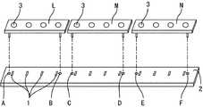
また、従来の多光軸光電スイッチは、かりにリフロー工程をなくしても、光軸ずれを招く別の要因があった。即ち、図5に示すように、従来の多光軸光電スイッチでは、複数の光電素子1が一列に配列された長尺状の基板2に対し、例えば、3つの光学ブロックL,M,Nが、その基板2の長手方向に並べて取り付けられ、各光学ブロックL,M,Nに備えたレンズ部3と各光電素子1とが対面する構成となっいた。また、基板2には、その両端と長手方向を概ね3等分した位置とに、位置決め孔A〜Fが形成され、ここに、各光学ブロックL,M,Nから突出した位置決め用ボス5が係合し、基板2と光学ブロックL,M,Nとが位置決めされる。
【0006】
ところが、光電素子1は、全て、基板2に対して、例えば図5における左側の位置決め孔Aを基準とした位置に実装されていた。このため、位置決め孔A以外の位置決め孔C〜Fに、位置決め用ボス5が係合される光学ブロックM,Nでは、光電素子1の配置の基準点(孔A)と、光学ブロックの位置合わせの基準点(孔C〜F)とが異なるので、公差が累積して大きくなり、光電素子1とレンズ部3との間で、位置ずれが生じる場合があった。
【0007】
本発明は、上記事情に鑑みてなされたもので、投光素子や受光素子といった光電素子とレンズ部との高精度で位置決め可能な多光軸光電スイッチの提供を目的とする。
【0008】
【課題を解決するための手段】
上記目的を達成するため、請求項1の発明に係る多光軸光電スイッチは、ベアチップ状の複数の光電素子が一列に配列されてワイヤーボンディングされると共に接着剤で固定され、リフロー半田が施されていない複数の光電素子用基板と、前記各光電素子用基板に対応して複数設けられ、それぞれに前記各光電素子に対向する複数のレンズ部が形成された複数の光学ブロックと、前記各光学ブロックと前記各光電素子用基板とに設けられて、前記各光電素子とレンズ部との光軸を合わせた状態で係合する凹凸係合部と、からなる複数のユニットと、前記光電素子以外の複数の電子部品が配置された長尺状のベース基板とを備え、前記複数のユニットは、全部のユニットに備えた前記光電素子が一直線に並ぶように、前記ベース基板上に配置されると共に、前記各ユニットの前記光電素子用基板に敷設した回路が前記ベース基板に敷設した回路に電気接続されてなるところに特徴を有する。
【0009】
請求項2の発明は、請求項1記載の多光軸光電スイッチにおいて、光電素子用基板上の回路とベース基板上の回路との電気接続は、ベース基板上の回路の一部からなる一方の接続端部と、光電素子用基板上の回路のうちその基板の縁部に配した部分からなる他方の接続端部とを半田付けて構成されているところに特徴を有する。
【0010】
【発明の作用及び効果】
<請求項1の発明>
請求項1の構成によれば、基板を、光電素子用基板と、光電素子以外の電子部品を配したベース基板とに分けたことで、光電素子用基板にリフロー半田を施さずに済むから、リフロー工程による光電素子の位置ずれは生じない。これに加え、各光学ブロックと各光電素子用基板とに設けた凹凸係合部を基準点として、光電素子用基板に光電素子を配置すれば、光電素子の配置と、光学ブロック及び光電素子用基板の位置合わせとが、同じ凹凸係合部を基準点として行われることとなり、従来のように公差が累積することがなくなる。これにより、光電素子と光学ブロックに設けたレンズ部とが正確に位置合わせされる。
【0011】
<請求項2の発明>
請求項2の構成によれば、光電素子用基板及びベース基板のそれぞれに設けた接続端部同士を、半田付けすることで、両基板の固定と、両基板に敷設された回路同士の接続とが一度に行われる。
【0012】
【発明の実施の形態】
以下、本発明の一実施形態を図1〜図4に基づいて説明する。
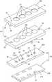
本実施形態の多光軸光電スイッチは、角筒状のケース10の内部に、電子部品を実装した基板20を収容して備える。
【0013】
ケース10の前面10Aには、一対の長孔11,11が長手方向に沿って並ぶように貫通形成されると共に、その前面10Aの両縁部に沿って一対のレール部12,12が設けられている。これらレール部12は、前面10Aから直立し、その先端部分が前面10A上にオーバーハングした係止部13となっており、この係止部13と前面10Aとの隙間に、長尺状の前面カバー14がスライド挿入される。また、ケース10の両端の開放口は、共に、パッキン15を挟んでキャップ16にて閉塞される。
【0014】
ケース10に収容される基板20は、長尺状のベース基板21と、一対の光電素子用基板22とからなる。ベース基板21は、前記ケース10とほぼ同じ長さをなし、ベース基板21のうち図1の左側を向いた表面21Aには、その左右の両縁部の長手方向に沿って、導電体をプリントしてなる複数のランド23が、例えば左右に6つずつ計12個設けられている。より詳細には、これらランド23は、図1におけるベース基板21の上方寄りの6つと、下方寄りの6つの2グループに分けられている。また、ベース基板21の裏面21Bには、図示しない抵抗、コンデンサ、トランジスタ等の光電素子以外の多くの電子部品が実装されると共に、上記電子部品を接続する回路がプリントされており、この回路と前記したランド23とがベース基板21を貫通して導通している。
【0015】
一方、光電素子用基板22は、ベース基板21を長手方向で2等分した長さより若干短くかつベース基板21より若干幅狭となっており、図2に示すように、長手方向に沿った2箇所に一対の位置決め孔24,24が貫通形成されている。光電素子用基板22のうち図2の上方を向いた表面22Aには、ベアチップ状の複数(例えば、4つ)の光電素子25が、長手方向に沿って一列に配されている。なお、多光軸光電スイッチには、投光用と受光用との2種類があり、投光用の多光軸光電スイッチでは、上記光電素子25は、投光素子で構成される一方、受光用の多光軸光電スイッチでは、上記光電素子は、受光素子で構成される。
【0016】
光電素子用基板22の表面22Aには、各光電素子25に接続される回路がプリントされると共に、この回路の端末部分で構成されたランド26が、表面22Aの左右両縁部に3つずつ計6個設けられている。これらランド26は、前記ベース基板21に2つにグループ分けして設けたランド23に対応している。
各光電素子用基板22には、表面22A側から光学ブロック30が組み付けられ、これにより、一対のユニット31(図1参照)が構成される。
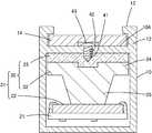
光学ブロック30は、共に樹脂成形品である光路基部32とレンズ板33とを合体させてなる。光路基部32は、前記光電素子用基板22とほぼ同じ矩形状をなした平板部34に、光電素子用基板22の各光電素子25に対応した複数(例えば、4つ)の孔34Aを貫通形成して、それら孔34Aの周縁部から光電素子用基板22に向け、円筒壁35を垂下して備える。また、平板部34から光電素子用基板22の各位置決め孔24に向けて、一対の位置決め支柱36が垂下されている。
【0017】
レンズ板33は、前記平板部34とほぼ同じ矩形状をなし、その平板部34に形成した孔34Aに対応した複数のレンズ部37を備える。レンズ部37は、レンズ板33のうち図2の上方を向いた表面33Aを、部分的に陥没させて凸レンズ状に形成してなる。また、レンズ板33の両端には、下面から前記光路基部32の平板部34に向けて、角柱ボス38が突設され、これらが前記平板部34に形成した位置決め用の角孔39に係合する。
【0018】
次に、本実施形態の多光軸光電スイッチを組み付ける手順を説明しつつ、本実施形態の作用・効果について説明する。
まず、基板20は、光電素子用基板22とベース基板21とに分けられて、別々に実装工程に送られる。
光電素子用基板22の表面22Aには、図2の左側に位置した位置決め孔24Aを基準点とした所定位置に、複数のベアチップ状の光電素子25がマウンタにて配されて、接着剤で基板22に固着される。そして、光電素子用基板22にプリントした回路にワイヤーボンディングされる。
【0019】
一方、ベース基板21には、その裏面21Bに、抵抗、コンデンサ、トランジスタ等の光電素子25以外の多くの電子部品(図示せず)が、マウンタにて実装され、リフロー工程にて半田付けされる。
【0020】
このように、本実施形態では、基板20を、光電素子25を配した光電素子用基板22と、光電素子25以外の電子部品を配したベース基板21とに分けたことで、光電素子用基板22にリフロー半田を施さずに済むようになり、光電素子25の位置ずれを防止することができる。一方、ベース基板21においては、光電素子の位置ずれを気にすることなく、リフロー工程にて迅速に半田処理を行える。
【0021】
次に、光路基部32の平板部34にレンズ板33を合体させる。このとき、レンズ板33の両端に設けた角柱ボス38を、平板部34に形成した位置決め角孔39に係合して熱溶着する。これにより、各レンズ部37と各円筒壁35とが芯合わせされた状態で、光路基部32とレンズ板33とが一体化されて、光学ブロック30が完成する。ここで、レンズ板33と光路基部32は、共に樹脂成形品であるので、レンズ板33と光路基部32との組み付け誤差は、図5に示した従来の基板2に形成された孔A〜Fの位置のばらつきに比べて、極めて小さく、無視することができる。
【0022】
次いで、完成した光学ブロック30を、実装工程を終了した光電素子用基板22に組み付ける。そのために、光学ブロック30(正確には、光路基部32)に設けた位置決め支柱36を、光電素子用基板22の表面22A側から各位置決め孔24に差し込む。すると、各円筒壁35の先端面が、光電素子用基板22の表面22Aのうち各光電素子25の回りに突き当てられたところで、支柱36が光電素子用基板22の裏面から突出するから、その突出部分を過熱して扁平状に潰す。これにより、各光電素子25が、光学ブロック30の各レンズ部37の中心に対面した状態で、それぞれ各光学ブロック30と各光電素子用基板22とが一体化されて、一対のユニット31が完成する。なお、光電素子用基板22の裏面において、位置決め孔24の開口縁を陥没させておき、潰された支柱36の先端が、その陥没部分に収まるようにしておくとよい。
【0023】
次いで、ユニット31,31を、ベース基板21に取り付ける。具体的には、各ユニット31に備えた光電素子用基板22の裏面を、ベース基板21の表面に宛い、ユニット31に一列にして備えた光電素子25が、互いに一直線に並ぶようにして、両ユニット31をベース基板21の幅方向の中央に配置する。そして、各ユニット31に設けたランド26とベース基板21に設けたランド23とを整合させて、両ランド23,26を覆うようにして半田付けする。これにより、ユニット31がベース基板21上に構造的に固定されると共に、両基板21,22にプリントされた各回路同士が電気接続され、多光軸光電スイッチの本体が完成する。
【0024】
次いで、多光軸光電スイッチの本体を、ケース10に内部にスライド挿入し、各ユニット31の平板部34に形成した下孔41とケース10の前面10Aに貫通形成したビス孔42とを整合させ、図4に示すように、そのビス孔42に通したビス43にて、多光軸光電スイッチの本体をケース10に固定する。次いで、前面カバー14を、ケース10の前面10Aに備えたレール部12,12の内側にスライド挿入し、最後に、ケース10の両端の開放口を、キャップ16,16にて閉塞して、全ての組み付けが完了する。
【0025】
このように、本実施形態の多光軸光電スイッチによれば、基板20を、光電素子用基板22と、光電素子以外の電子部品を配したベース基板21とに分けたことで、光電素子用基板22にリフロー半田を施さずに済むようになり、光電素子25の位置ずれを防止することができる。これに加え、光電素子用基板22に光電素子25を配置するときの基準孔となる孔24Aに、光学ブロック30の位置決め支柱36を係合させて、両者を位置決めしたから、従来のように公差が累積することがなくなり、光電素子25とレンズ部37とを、正確に位置合わせすることができる。しかも、光電素子用基板22及びベース基板21のそれぞれに設けたランド23,26同士を、半田付けすることで、各基板21,22の固定と、各基板21,22に敷設された回路同士の接続とが一度に行われ、両基板21,22の組み付け効率がよくなる。
【0026】
<他の実施形態>
本発明は、前記実施形態に限定されるものではなく、例えば、以下に説明するような実施形態も本発明の技術的範囲に含まれ、さらに、下記以外にも要旨を逸脱しない範囲内で種々変更して実施することができる。
(1)前記実施形態の多光軸光電スイッチには、ユニットが2つそなえられていたが、3つ以上のユニットを備えたものであってもよい。
【0027】
(2)前記実施形態では、光電ブロック30は、レンズ板33と光路基部32とを組み付けて完成される構成であったが、これらを一体に成形してなるものであってもよい。
【0028】
(3)前記実施形態では、光電素子用基板22とベース基板21とを、互いに重ね合わせるようにして固着したが、例えば、光電素子用基板の端部を、ベース基板に突き合わせて、光電素子用基板が、ベース基板から起立した状態にして固着してもよい。この場合は、光電素子用基板の突き合わせ部分の縁部に、ランドを配置すればよい。
【0029】
(4)前記実施形態において、光学ブロック30の位置決め支柱36を、例えば、光電素子用基板22のみならず、ベース基板21をも貫通させる構成とし、そのベース基板21の裏面側で、支柱36の先端を潰してもよい。これにより、例えば、両基板21,22が固定されて状態で、両ランド23,26の半田付けを行えるから、作業効率が向上する。
【図面の簡単な説明】
【図1】本発明の一実施形態に係る多光軸光電スイッチの分解斜視図
【図2】ユニットの分解斜視図
【図3】多光軸光電スイッチの断面図
【図4】多光軸光電スイッチの断面図
【図5】従来の多光軸光電スイッチに備えた基板の斜視図
【符号の説明】
20…基板
21…ベース基板
22…光電素子用基板
23,26…ランド
24…孔(凹凸係合部)
25…光電素子
30…光学ブロック
31…ユニット
36…支柱(凹凸係合部)
37…レンズ部
38…角柱ボス
39…角孔[0001]
BACKGROUND OF THE INVENTION
The present invention relates to a multi-optical axis photoelectric switch.
[0002]
[Prior art]
In general, a plurality of photoelectric elements (light projecting elements or light receiving elements) are mounted on a substrate provided for a multi-optical axis photoelectric switch, and many electronic components such as resistors, capacitors, and transistors are mounted. .
[0003]
[Problems to be solved by the invention]
By the way, there are the following two means for mounting the above-described photoelectric element on the substrate. One is to use a photoelectrically packaged resin element and place it at a predetermined position on the substrate for reflow soldering. However, according to this means, the photoelectric element may be displaced from the normal position during reflow soldering, and the optical axis may be displaced.
[0004]
The other is to use a bare chip that is not packaged with resin as the photoelectric element, fix it to the substrate with an adhesive, and perform wire bonding, and then pot the resin. It is. However, even with this means, in a conventional multi-optical axis photoelectric switch, after mounting a bare chip photoelectric element on a substrate, many electronic components such as chip resistors, capacitors, transistors, and ICs are mounted on the substrate. Since the adhesive was melted by the heat of the reflow, the photoelectric element was displaced from the normal position, the potting resin was melted, and the light projecting direction from the photoelectric element was In some cases, the optical axis is shifted by being directed in a direction different from the normal direction.
[0005]
Further, the conventional multi-optical axis photoelectric switch has another factor that causes an optical axis shift even if the reflow process is omitted. That is, as shown in FIG. 5, in a conventional multi-optical axis photoelectric switch, for example, three optical blocks L, M, and N are provided on a
[0006]
However, all of the
[0007]
The present invention has been made in view of the above circumstances, and an object of the present invention is to provide a multi-optical axis photoelectric switch capable of positioning a photoelectric element such as a light projecting element and a light receiving element with a lens unit with high accuracy.
[0008]
[Means for Solving the Problems]
To achieve the above object, the multi-optical axis photoelectric switch according to a first aspect of the invention, are arranged in a bare chip form of a plurality of photoelectric elements one rowis fixed by the wire bondingRutotomoni adhesive, reflow soldering is performed A plurality of photoelectric element substrates, a plurality of optical blocks provided corresponding to the respective photoelectric element substrates, and formed with a plurality of lens portions respectively facing the respective photoelectric elements, and the respective optical elements Aplurality of units provided on the block and each photoelectric element substrate and engaged with the respective photoelectric elements and the lens unit in a state where the optical axes are aligned,and other than the photoelectric elements of the of a plurality of elongated base board on which electronic components are arranged,the plurality of units, as the photoelectric element having the whole unit is aligned, placed on the base substrate Rutotomoni, having characterized in that the circuit which is laid on the photoelectric device substrate of each unit becomes electrically connected to the circuits laid on the base substrate.
[0009]
According to a second aspect of the present invention, in the multi-optical axis photoelectric switch according to the first aspect, the electrical connection between the circuit on the photoelectric element substrate and the circuit on the base substrate is a part of the circuit on the base substrate. It is characterized in that it is configured by soldering the connection end portion and the other connection end portion composed of the portion disposed on the edge portion of the circuit on the photoelectric element substrate.
[0010]
[Action and effect of the invention]
<Invention of
According to the configuration of
[0011]
<Invention of
According to the configuration of
[0012]
DETAILED DESCRIPTION OF THE INVENTION
Hereinafter, an embodiment of the present invention will be described with reference to FIGS.
The multi-optical axis photoelectric switch of the present embodiment includes a
[0013]
The
[0014]
The
[0015]
On the other hand, the
[0016]
A circuit connected to each
Each
The
[0017]
The
[0018]
Next, the operation and effect of this embodiment will be described while explaining the procedure for assembling the multi-optical axis photoelectric switch of this embodiment.
First, the
On the
[0019]
On the other hand, many electronic components (not shown) other than the
[0020]
As described above, in this embodiment, the
[0021]
Next, the
[0022]
Next, the completed
[0023]
Next, the
[0024]
Next, the main body of the multi-optical axis photoelectric switch is slid into the
[0025]
As described above, according to the multi-optical axis photoelectric switch of the present embodiment, the
[0026]
<Other embodiments>
The present invention is not limited to the above-described embodiment. For example, the embodiments described below are also included in the technical scope of the present invention, and various other than the following can be made without departing from the scope of the invention. It can be changed and implemented.
(1) Although the multi-optical axis photoelectric switch of the above embodiment has two units, it may have three or more units.
[0027]
(2) In the above-described embodiment, the
[0028]
(3) In the above-described embodiment, the
[0029]
(4) In the above-described embodiment, the
[Brief description of the drawings]
1 is an exploded perspective view of a multi-optical axis photoelectric switch according to an embodiment of the present invention. FIG. 2 is an exploded perspective view of a unit. FIG. 3 is a cross-sectional view of a multi-optical axis photoelectric switch. Cross-sectional view of switch [FIG. 5] Perspective view of substrate provided in conventional multi-optical axis photoelectric switch [Explanation of symbols]
20 ...
25 ...
37 ...
Claims (2)
Translated fromJapanese前記各光電素子用基板に対応して複数設けられ、それぞれに前記各光電素子に対向する複数のレンズ部が形成された複数の光学ブロックと、
前記各光学ブロックと前記各光電素子用基板とに設けられて、前記各光電素子とレンズ部との光軸を合わせた状態で係合する凹凸係合部と、からなる複数のユニットと、
前記光電素子以外の複数の電子部品が配置された長尺状のベース基板とを備え、
前記複数のユニットは、全部のユニットに備えた前記光電素子が一直線に並ぶように、前記ベース基板上に配置されると共に、前記各ユニットの前記光電素子用基板に敷設した回路が前記ベース基板に敷設した回路に電気接続されてなることを特徴とする多光軸光電スイッチ。Bare chip form of a plurality of photoelectric elements is an array in a roware fixed at Rutotomoni adhesive is wirebonding, a plurality of substrate for a photoelectricelement reflow soldering is not applied,
A plurality of optical blocks provided corresponding to the respective photoelectric element substrates, each having a plurality of lens portions facing the respective photoelectric elements;
Aplurality of units comprising concave and convex engaging portions that are provided on the optical blocks and the photoelectric element substrates, and are engaged with the optical axes of the photoelectric elements and the lens portions aligned,
A long base substrate on which a plurality of electronic components other than the photoelectric elements are arranged,
The plurality of units are arranged on the base substrate so that the photoelectric elements included in all the units are aligned, and a circuit laid on the photoelectric element substrate of each unit is formed on the base substrate. A multi-optical axis photoelectric switch characterized by being electrically connected to a laid circuit.
Priority Applications (1)
| Application Number | Priority Date | Filing Date | Title |
|---|---|---|---|
| JP30987399AJP3734992B2 (en) | 1999-10-29 | 1999-10-29 | Multi-optical axis photoelectric switch |
Applications Claiming Priority (1)
| Application Number | Priority Date | Filing Date | Title |
|---|---|---|---|
| JP30987399AJP3734992B2 (en) | 1999-10-29 | 1999-10-29 | Multi-optical axis photoelectric switch |
Publications (2)
| Publication Number | Publication Date |
|---|---|
| JP2001135208A JP2001135208A (en) | 2001-05-18 |
| JP3734992B2true JP3734992B2 (en) | 2006-01-11 |
Family
ID=17998339
Family Applications (1)
| Application Number | Title | Priority Date | Filing Date |
|---|---|---|---|
| JP30987399AExpired - Fee RelatedJP3734992B2 (en) | 1999-10-29 | 1999-10-29 | Multi-optical axis photoelectric switch |
Country Status (1)
| Country | Link |
|---|---|
| JP (1) | JP3734992B2 (en) |
Cited By (1)
| Publication number | Priority date | Publication date | Assignee | Title |
|---|---|---|---|---|
| US10509159B2 (en) | 2016-08-22 | 2019-12-17 | Samsung Electronics Co., Ltd. | Light source module and backlight assembly having the same |
Families Citing this family (4)
| Publication number | Priority date | Publication date | Assignee | Title |
|---|---|---|---|---|
| JP3927503B2 (en) | 2003-01-20 | 2007-06-13 | 株式会社キーエンス | Multi-axis photoelectric sensor |
| JP2005300399A (en)* | 2004-04-14 | 2005-10-27 | Keyence Corp | Multioptical axses photoelectronic sensor |
| JP6084522B2 (en)* | 2013-06-21 | 2017-02-22 | 株式会社キーエンス | Multi-axis photoelectric sensor |
| KR102341530B1 (en)* | 2020-03-03 | 2021-12-22 | 주식회사 오토닉스 | Sensor |
- 1999
- 1999-10-29JPJP30987399Apatent/JP3734992B2/ennot_activeExpired - Fee Related
Cited By (1)
| Publication number | Priority date | Publication date | Assignee | Title |
|---|---|---|---|---|
| US10509159B2 (en) | 2016-08-22 | 2019-12-17 | Samsung Electronics Co., Ltd. | Light source module and backlight assembly having the same |
Also Published As
| Publication number | Publication date |
|---|---|
| JP2001135208A (en) | 2001-05-18 |
Similar Documents
| Publication | Publication Date | Title |
|---|---|---|
| US7791901B2 (en) | Stand-off mounting apparatus for discrete electrical components | |
| US5410450A (en) | Internal wiring structure of a semiconductor device | |
| US4793058A (en) | Method of making an electrical connector | |
| FR2696283A3 (en) | Adaptor to connect electronic control probe to electronic module - has flexible substrate on which tracks are formed connecting the module to contacts spaced to be compatible with probe | |
| US20060220636A1 (en) | Highly stable piezoelectric oscillator | |
| CN101267964A (en) | Combined fixing and connecting system for electrical components on circuit boards arranged one above the other | |
| JP4829306B2 (en) | Frame packaged array device for holding electronic components | |
| KR950010891B1 (en) | Electronic circuits and a method for their manufacture by means of ultrasonic welding | |
| US4338717A (en) | Method for fabricating a light emitting diode display socket | |
| JP3734992B2 (en) | Multi-optical axis photoelectric switch | |
| JP3022049B2 (en) | Mounting method of light emitting diode of chip component type | |
| US4588239A (en) | Programmed socket | |
| JP2000236156A (en) | Mounting optical module on circuit board | |
| JP2570336B2 (en) | Hybrid integrated circuit device | |
| US6191369B1 (en) | Printed circuit board having a marker trace for component alignment | |
| KR100651465B1 (en) | Manufacturing method of electronic circuit module and integrated circuit device and electronic circuit module using the same | |
| JPH03126290A (en) | Printed wiring board | |
| KR100538145B1 (en) | Module with different boards and method for assembly the module | |
| JPH0737360Y2 (en) | Integrated circuit parts | |
| JP3695474B2 (en) | Optical encoder and method for attaching fixed side element of optical encoder | |
| JP2750595B2 (en) | Connection members for electronic components for surface mounting | |
| JP2550879B2 (en) | Semiconductor device mounting structure | |
| JPH0343746Y2 (en) | ||
| JPH0439668Y2 (en) | ||
| JP2581397B2 (en) | Mounting / connection board for multi-pin circuit elements |
Legal Events
| Date | Code | Title | Description |
|---|---|---|---|
| A977 | Report on retrieval | Free format text:JAPANESE INTERMEDIATE CODE: A971007 Effective date:20040901 | |
| A131 | Notification of reasons for refusal | Free format text:JAPANESE INTERMEDIATE CODE: A131 Effective date:20050210 | |
| A521 | Written amendment | Free format text:JAPANESE INTERMEDIATE CODE: A523 Effective date:20050411 | |
| TRDD | Decision of grant or rejection written | ||
| A01 | Written decision to grant a patent or to grant a registration (utility model) | Free format text:JAPANESE INTERMEDIATE CODE: A01 Effective date:20051018 | |
| A61 | First payment of annual fees (during grant procedure) | Free format text:JAPANESE INTERMEDIATE CODE: A61 Effective date:20051020 | |
| R150 | Certificate of patent or registration of utility model | Free format text:JAPANESE INTERMEDIATE CODE: R150 | |
| FPAY | Renewal fee payment (event date is renewal date of database) | Free format text:PAYMENT UNTIL: 20081028 Year of fee payment:3 | |
| FPAY | Renewal fee payment (event date is renewal date of database) | Free format text:PAYMENT UNTIL: 20111028 Year of fee payment:6 | |
| FPAY | Renewal fee payment (event date is renewal date of database) | Free format text:PAYMENT UNTIL: 20111028 Year of fee payment:6 | |
| FPAY | Renewal fee payment (event date is renewal date of database) | Free format text:PAYMENT UNTIL: 20121028 Year of fee payment:7 | |
| FPAY | Renewal fee payment (event date is renewal date of database) | Free format text:PAYMENT UNTIL: 20121028 Year of fee payment:7 | |
| S533 | Written request for registration of change of name | Free format text:JAPANESE INTERMEDIATE CODE: R313533 | |
| FPAY | Renewal fee payment (event date is renewal date of database) | Free format text:PAYMENT UNTIL: 20121028 Year of fee payment:7 | |
| R350 | Written notification of registration of transfer | Free format text:JAPANESE INTERMEDIATE CODE: R350 | |
| FPAY | Renewal fee payment (event date is renewal date of database) | Free format text:PAYMENT UNTIL: 20121028 Year of fee payment:7 | |
| FPAY | Renewal fee payment (event date is renewal date of database) | Free format text:PAYMENT UNTIL: 20131028 Year of fee payment:8 | |
| R250 | Receipt of annual fees | Free format text:JAPANESE INTERMEDIATE CODE: R250 | |
| R250 | Receipt of annual fees | Free format text:JAPANESE INTERMEDIATE CODE: R250 | |
| R250 | Receipt of annual fees | Free format text:JAPANESE INTERMEDIATE CODE: R250 | |
| R250 | Receipt of annual fees | Free format text:JAPANESE INTERMEDIATE CODE: R250 | |
| R250 | Receipt of annual fees | Free format text:JAPANESE INTERMEDIATE CODE: R250 | |
| LAPS | Cancellation because of no payment of annual fees |