JP3734530B2 - Planar cold cathode electron emitter and field emission device - Google Patents
Planar cold cathode electron emitter and field emission deviceDownload PDFInfo
- Publication number
- JP3734530B2 JP3734530B2JP15115795AJP15115795AJP3734530B2JP 3734530 B2JP3734530 B2JP 3734530B2JP 15115795 AJP15115795 AJP 15115795AJP 15115795 AJP15115795 AJP 15115795AJP 3734530 B2JP3734530 B2JP 3734530B2
- Authority
- JP
- Japan
- Prior art keywords
- layer
- opening
- conductive
- electron
- insulating layer
- Prior art date
- Legal status (The legal status is an assumption and is not a legal conclusion. Google has not performed a legal analysis and makes no representation as to the accuracy of the status listed.)
- Expired - Fee Related
Links
- 239000000463materialSubstances0.000claimsdescription46
- 239000000758substrateSubstances0.000claimsdescription19
- 230000003287optical effectEffects0.000claims1
- 239000010410layerSubstances0.000description205
- 230000005684electric fieldEffects0.000description30
- VYPSYNLAJGMNEJ-UHFFFAOYSA-NSilicium dioxideChemical compoundO=[Si]=OVYPSYNLAJGMNEJ-UHFFFAOYSA-N0.000description14
- 239000010432diamondSubstances0.000description13
- 229910003460diamondInorganic materials0.000description12
- 238000000605extractionMethods0.000description12
- 229910052751metalInorganic materials0.000description8
- 239000002184metalSubstances0.000description8
- 238000002347injectionMethods0.000description7
- 239000007924injectionSubstances0.000description7
- 235000012239silicon dioxideNutrition0.000description7
- 239000000377silicon dioxideSubstances0.000description7
- 238000004088simulationMethods0.000description7
- 238000009826distributionMethods0.000description6
- 229910004298SiO 2Inorganic materials0.000description5
- 238000005094computer simulationMethods0.000description4
- 239000004020conductorSubstances0.000description4
- 230000015572biosynthetic processEffects0.000description3
- 238000006243chemical reactionMethods0.000description3
- 238000009413insulationMethods0.000description3
- 238000000059patterningMethods0.000description3
- PXHVJJICTQNCMI-UHFFFAOYSA-NNickelChemical compound[Ni]PXHVJJICTQNCMI-UHFFFAOYSA-N0.000description2
- 239000003575carbonaceous materialSubstances0.000description2
- 230000015556catabolic processEffects0.000description2
- 238000010586diagramMethods0.000description2
- 239000004065semiconductorSubstances0.000description2
- 239000003381stabilizerSubstances0.000description2
- 230000000007visual effectEffects0.000description2
- OKTJSMMVPCPJKN-UHFFFAOYSA-NCarbonChemical compound[C]OKTJSMMVPCPJKN-UHFFFAOYSA-N0.000description1
- ZOKXTWBITQBERF-UHFFFAOYSA-NMolybdenumChemical compound[Mo]ZOKXTWBITQBERF-UHFFFAOYSA-N0.000description1
- RTAQQCXQSZGOHL-UHFFFAOYSA-NTitaniumChemical compound[Ti]RTAQQCXQSZGOHL-UHFFFAOYSA-N0.000description1
- 229910052782aluminiumInorganic materials0.000description1
- XAGFODPZIPBFFR-UHFFFAOYSA-NaluminiumChemical compound[Al]XAGFODPZIPBFFR-UHFFFAOYSA-N0.000description1
- 238000004458analytical methodMethods0.000description1
- 229910052799carbonInorganic materials0.000description1
- PMHQVHHXPFUNSP-UHFFFAOYSA-Mcopper(1+);methylsulfanylmethane;bromideChemical compoundBr[Cu].CSCPMHQVHHXPFUNSP-UHFFFAOYSA-M0.000description1
- 230000007423decreaseEffects0.000description1
- 230000007812deficiencyEffects0.000description1
- 230000000694effectsEffects0.000description1
- 238000010894electron beam technologyMethods0.000description1
- 238000005530etchingMethods0.000description1
- 238000001459lithographyMethods0.000description1
- 238000004020luminiscence typeMethods0.000description1
- 238000004519manufacturing processMethods0.000description1
- 238000005259measurementMethods0.000description1
- 150000002739metalsChemical class0.000description1
- 238000000034methodMethods0.000description1
- 229910052750molybdenumInorganic materials0.000description1
- 239000011733molybdenumSubstances0.000description1
- 229910052759nickelInorganic materials0.000description1
- 239000002245particleSubstances0.000description1
- 230000000149penetrating effectEffects0.000description1
- 230000002093peripheral effectEffects0.000description1
- 239000000243solutionSubstances0.000description1
- 125000006850spacer groupChemical group0.000description1
- 239000002344surface layerSubstances0.000description1
- 229910052719titaniumInorganic materials0.000description1
- 239000010936titaniumSubstances0.000description1
- WFKWXMTUELFFGS-UHFFFAOYSA-NtungstenChemical compound[W]WFKWXMTUELFFGS-UHFFFAOYSA-N0.000description1
- 229910052721tungstenInorganic materials0.000description1
- 239000010937tungstenSubstances0.000description1
- 238000007740vapor depositionMethods0.000description1
Images


Classifications
- H—ELECTRICITY
- H01—ELECTRIC ELEMENTS
- H01J—ELECTRIC DISCHARGE TUBES OR DISCHARGE LAMPS
- H01J3/00—Details of electron-optical or ion-optical arrangements or of ion traps common to two or more basic types of discharge tubes or lamps
- H01J3/02—Electron guns
- H01J3/021—Electron guns using a field emission, photo emission, or secondary emission electron source
- H—ELECTRICITY
- H01—ELECTRIC ELEMENTS
- H01J—ELECTRIC DISCHARGE TUBES OR DISCHARGE LAMPS
- H01J1/00—Details of electrodes, of magnetic control means, of screens, or of the mounting or spacing thereof, common to two or more basic types of discharge tubes or lamps
- H01J1/02—Main electrodes
- H01J1/30—Cold cathodes, e.g. field-emissive cathode
- H01J1/304—Field-emissive cathodes
- H01J1/3042—Field-emissive cathodes microengineered, e.g. Spindt-type
- H—ELECTRICITY
- H01—ELECTRIC ELEMENTS
- H01J—ELECTRIC DISCHARGE TUBES OR DISCHARGE LAMPS
- H01J2201/00—Electrodes common to discharge tubes
- H01J2201/30—Cold cathodes
- H01J2201/304—Field emission cathodes
- H01J2201/30446—Field emission cathodes characterised by the emitter material
- H01J2201/30453—Carbon types
- H01J2201/30457—Diamond
Landscapes
- Cathode-Ray Tubes And Fluorescent Screens For Display (AREA)
- Cold Cathode And The Manufacture (AREA)
- Electrodes For Cathode-Ray Tubes (AREA)
Description
Translated fromJapanese【0001】
【産業上の利用分野】
本発明は一般的に冷陰極電子放出素子(cold cathode emission devices)に関し、特にダイアモンド物質を用いた電子エミッタ(electron emitter)および低仕事関数(work function)物質を用いた同様のエミッタに関するものである。
【0002】
【従来の技術】
冷陰極電子エミッタは、主に電界放出素子(field emission device)を含み、これは、先端表面における電界を高めて十分に電子を引き出す(draw off)即ち放出するために、元来非常に鋭い先端を必要とするものであった。一般的に、抽出電極(extraction electrode)は先端を含む面内に形成され、この先端を完全に包囲して、チップと抽出電極との間に抽出電位を与えるように配置される。これらの素子に伴う主要な問題は、非常に鋭い先端の製造が難しいことである。更に、一旦チップを製造すると、電界放出素子を動作させるに連れて、チップが劣化する即ち粒子(particle)を失う傾向がある。
【0003】
これらの問題を解決するために、エミッタに低仕事関数物質を利用しようとする動きがある。ダイアモンド・エミッタを利用する場合のように、場合によっては、合理的な電位の印加で必要とする電子放出量を確保しつつ、エミッタを事実上平面構造とすることもできる。かかる構造の例は、"Electron Device Employing a Low/Negative Electron Affinity Electron Source"と題され、本願と同一譲受人に譲渡された米国特許第5,283,501号に開示されている。
【0004】
【発明が解決しようとする課題】
これら低仕事関数素子においても、抽出格子電流(extraction grid current)が多すぎるという問題が存在する。鋭い先端を用いる場合、放出は自動的にエミッタの中央で行われので、電子流が陽極/スクリーンに衝突する前に、それを合焦させればよい。平面エミッタを用いる場合、電界内のどこででもその表面から電子を放出し得るので、結果的に放出電子の大部分が直接抽出電極に流れる。抽出電極に電流が流れると、素子の効率および動作特性を大きく低下させることになる。
【0005】
したがって、上述の従来技術の欠陥の少なくともいくつかを克服する平面冷陰極放出素子が必要とされている。
【0006】
本発明の目的の1つは、電子放出制御のためにパターニングされた金属を用いた新規で改良された冷陰極電子エミッタを提供することである。
【0007】
本発明の他の目的は、抽出電極電流を大幅に低減した、新規で改良された冷陰極電子エミッタを提供することである。
【0008】
本発明の更に他の目的は、誘電体したがって素子のブレークダウン(breakdown)を低下させる新規で改良された冷陰極電子エミッタを提供することである。
【0009】
本発明の更に他の目的は、周囲の誘電体への電子注入を減少或いは解消する新規で改良された冷陰極電子エミッタを提供することである。
【0010】
本発明の更に他の目的は、動作特性および効率を改善した、新規で改良された冷陰極電子エミッタを提供することである。
【0011】
【課題を解決するための手段】
上述のおよびその他の問題の解決、および上述のおよびその他の目的の実現は、比較的平面な表面を有する基板と、この基板表面上に支持され、電子を放出する低仕事関数電子放出物質とを含む、平面冷陰極電子エミッタによって達成される。電子放出物質層上に接触導電層を配置し、それを貫通する開口を規定する。接触導電層上に絶縁層を配置し、実質的に接点導電層の開口の延長上にありかつ周辺が整合された開口を規定する。更に、絶縁層上に導電ゲート層を配置する。接触導電層は、実質的に開口の中央で放出が生じるように、電界電位(field potential)を形成する。
【0012】
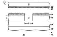
【実施例】
ここで図1を参照すると、電界放出素子12に組み込まれた平面冷陰極電子エミッタ10の実施例を示す、部分的側面概略図が示されている。エミッタ10は、ダイアモンド等のような低仕事関数物質層14を有する基板13を含む。絶縁層15を層14上に付着し、それを貫通する開口17を規定する。一般的に、絶縁層15は二酸化シリコンのような酸化物で形成される。導電層18を絶縁層15上に堆積(deposite)し、電界放出素子12の抽出ゲート(extraction gate)を形成する。光学的に透明な目視スクリーン構造体20は、陰極ルミネセンス物質層(cathodoluminescent material layer)のような物質層22および導電陽極層23が付着された透明スクリーン21を含む。
【0013】
層14(陰極)に対して十分な正電圧を陽極23に印加すると、層14から電子が放出され、陽極23と層14との間の電界によって加速され、陽極23に衝突し、結果的に層22から光子(光)が放出される。層14上に誘電体即ち絶縁層15および導電ゲート層18を配置すると、ゲート層18の電圧を変調することによって、層14の表面における電界を制御することができる。したがって、ゲート層18は電子放出を制御し、トライオード型(triode type)の素子が形成される。典型的に、陽極/陰極バイアスによる電界は、層14から電子を放出させるのに必要なバイアスよりも小さい。
【0014】
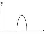
トライオード素子のコンピュータ解析によって、放出プロセスは少なくとも指数関数的に熱電子的(thermionic)であり、フォーラ−ノルドハイム(Fowler-Nordheim)に近似することが示される。これは、表面電界への依存性において単一の指数関数よりも更に鋭い(steep)ものである。したがって、層14の表面に沿った空間電界強度特性に小さな変化があると、空間電子放出率(spatial electron emission rates)に大きな変化が生じることになる。
【0015】
開口17の直径D、絶縁層15の厚さh=Dとした図1の構造では、図2に示すように、層14の表面電界はゲート(層18)の縁で最大となり、開口17の中心で落ち込む(slump)。図2を参照すると、図1の構造における空間電界強度ε対位置Pの関係がグラフで示されており、開口17の縁で電界強度の破壊(break)が生じている。図示した具体的な実施例では、開口17の中心における電界強度量の落ち込みは約3%である。電界は層18の縁で最大となり、放出電流を層18に集中させ、放出される電子の殆どを層18に集めるため、その結果ゲート電流が高くなると共に電界放出素子12の動作は非効率的となる。
【0016】
図1の構造における別の問題は、層18をダイアモンドで形成する場合、一般的に二酸化シリコン(SiO2)の絶縁層15と直接接触することである。Capacitance-Voltage Measurements on Metal-SiO2-Diamond Structures Fabricated with (100)- and (111)- Oriented Substrates", IEEE Transactions on Electron Devices,Vol. 38, No, 3 (1991年3月)においてGeis et al.によって指摘されたように、ダイアモンドはSiO2内に効果的に電子を注入することができる。MOSFETやEPROMにおいて熱電子の信頼性問題によって示されたように、ある時間にわたる電荷の注入は、誘電体が結果的に破壊される(通電する)原因となる。したがって、図1の電界放出素子12には、固有の信頼性問題がある。
【0017】
次に図3を参照すると、本発明による電界放出素子32内に組み込まれた平面冷陰極電子エミッタ30の実施例の部分的側面概略図が示されている。エミッタ30は、例えば、ダイアモンド、ダイアモンド状炭素物質、非結晶性ダイアモンド状炭素物質、窒化アルミニウム物質等のような、表面仕事関数が約1.0電子ボルト未満の電界放出物質のような、低仕事関数物質層34が表面に配置された基板33を含む(本開示では、「配置(disposed)」という用語は、蒸着(vapor deposition)、エピタキシャル成長またはその他の成長、或いはその他の形成による、層の形成を意味する)。また、層34は、例えば、金属または安定物質(ballast material)およびダイアモンド等の二重層(bilayer)のような複数の層を付着したり、金属、安定物質およびダイアモンドの三重層(trilayer)等でも形成可能であることは理解されよう。
【0018】
金属、高濃度にドープされた半導体物質等のような導電接触層35を層34の表面に配置する。接触層35をパターニングしてそれを貫通する開口37を規定する。絶縁層38を層35上に配置し、それを貫通する開口39を規定する。一般的に、絶縁層38は、二酸化シリコン(SiO2)のような酸化物で形成される。導電層40を絶縁層38上に配置し、電界放出素子32の抽出ゲートを形成する。導電層40をパターニングしてそれを貫通する開口41を規定する。層35を貫通する開口37、層38を貫通する開口39、および層40を貫通する開口41は、実質的に同一の広がりを有し(coextensive)、層34,38,40を貫通する1つの連続開口を形成するように周囲が整合されている。場合によっては、開口37,39,41の縁は、パターニング、エッチング等の誤差のために、周囲が僅かにずれることがあるが、かかる誤差は「実質的」同一の範時に属するものとする。本実施例では、開口37,39,41も断面が円形であり同心状に整合されているが、特定用途では他の形状も採用可能であることは理解されよう。
【0019】
光学的に透明な目視スクリーン構造体42は、透明スクリーン43を含み、その上に陰極ルミネセンス物質層のような物質層44と導電陽極層45とが形成されている。場合によっては、層44を導電性物質で形成するか、或いは層44に導電性物質を含ませることによって、電荷を表面から遠ざけるように導く陽極として作用させる。また、場合によっては、陰極ルミネセンス物質層が良く導電しないため、付加導電物性質層を設けることもある。本実施例では、層45は透明でなければならず(例えばITO等)、透明スクリーン43の表面に付着され、更に陰極ルミネセンス物質層44が層45の表面に付着される。この構成によって、速度の低い電子が層45を通過して層44に到達する必要がなくなるので、スクリーン・バイアスを低くすることが可能となる(約<3kv)。
【0020】
図3の具体的な構造では、全体的に図4に示すように、開口37,39,41の直径および絶縁層38の厚さがhの場合、層34の表面電界はゲート(層40)の中央で最大となり、開口37の縁でゼロに低下する。図4は、図3の構造における、垂直方向の空間電界強度と位置Pとの関係を表わすグラフである。
【0021】
本発明の具体的実施例では、層34をダイアモンド状炭素で形成し、接触層35を金属で形成し、絶縁層38を二酸化シリコン(SiO2)で形成する。絶縁層38の厚さをh=Dとし、接触層35の厚さをhの20%とした場合、図4に示すように、層34の表面に軸対称放物線状電界分布(centered parabolic field distribution)が得られる。したがって、平面冷陰極電子エミッタ30の放出電流は、開口37,39,41によって形成される開口の中心に集中する。この新たな電界プロファイルが形成される理由は、接触層35のために垂直方向電界分布が層34表面上の開口37の縁でゼロとなることを認識することによって、最も容易に理解されよう。
【0022】
接触層35の厚さを変化させることによって、電界特性の形状が変化する。即ち、接触層35を厚くするに連れて、電界特性のピークが先鋭化し、接触層35を薄くするに連れて、平面的な電界特性になるが、軸対称の形状は変わらない。また、接触層35を厚くすると、表面層34が遮蔽されるので、電界ピーク値も減少する。絶縁層38の厚さh、接触層35の厚さ、および開口37の直径Dに対する通常の合理的な値は、D=h=1ミクロン、接触層35の厚さは0.2ミクロン、そしてゲート(層40)の厚さは0.2ミクロンである。
【0023】
図5を参照すると、トライオード型電界放出素子50(図3の電界放出素子32に類似する)を模した半断面図が、コンピュータ・シミュレーションによって描かれている。このコンピュータ・シミュレーションでは、表面51が、導電層52、誘電体層53およびその上に配置されたゲート層54から成り、これらを貫通する開口55が規定されたエミッタとして機能する。シミュレーション境界(simulation boundary)56(光学的に透明な目視スクリーン構造体42を表わす)が、表面51から約4ミクロンに位置付けられる。層52,53,54の半分が、それを貫通して規定された開口55の半分と共に示されている。シミュレーション境界56の上にある数字(legend)は、開口55の中心からの距離をミクロンで示すものである。一群の線57は等電位線であり、一群の破線58は電子の経路、即ちシミュレーション境界56への軌道を示す。
【0024】
図3の電界放出素子32の別の特徴が、図5のコンピュータ・シミュレーションに描かれている。このシミュレーションは、接触層(contact layer)35(層52)の存在に起因する電子軌道の変更即ち合焦(focusing)を示している。接触層35がないと、電子の軌道は発散し、ゲート開口41を出て拡散する(図示せず)。接触層35の縁における垂直方向電界は接触層35によってゼロにされているので、接触層35の合焦効果は、電界遅延(field retardation)による電界線の歪み(warping)によるものである。
【0025】
図3の電界放出素子32の他の特徴は、接触層35がダイアモンド層34と絶縁層38(二酸化シリコンSiO2で形成される)との間に挟持され、ダイアモンドから二酸化シリコンへの電子の注入を防止することである。電子の誘電体への直接注入を防止することによって、注入によって引き起こされる信頼性の問題を解消することができる。
【0026】
次に図6を参照すると、本発明による電界放出素子62に組み込まれた平面冷陰極電子エミッタ60の他の実施例の部分的側面概略図が示されている。エミッタ60は基板63を含み、この基板63の表面に金属、高濃度にドープされた半導体物質等のような導電性物質層62が配置されている。層34について上述したものと同様の、低仕事関数物質層64を層62の表面に配置する。導電接触層65を層64の表面に配置し、それを貫通する開口を規定する。層65上に絶縁層68を配置し、それを貫通する開口を規定する。絶縁層68上に導電層70を配置し、電界放出素子62の抽出ゲートを形成し、それを貫通する開口を規定するようにパターニングを行う。層65、層68および層70を貫通する開口は実質的に同一の広がりを有し、層65,68,70によって完全に包囲された1つの連続開口71を形成するように、同軸状に周辺が整合されている。光学的に透明な目視スクリーン構造体72は透明スクリーン73を含み、その上に、陰極ルミネセンス物質層のような物質層74と導電層75とが形成されている。本実施例では、層75が層74(陽極接点を形成する)を被覆している。
【0027】
電子エミッタ60の接触層65は、実質的に上述の図3の電子エミッタ30の層35のように動作する。導電層62を付加したために、低仕事関数物質層64との接触が強化され、導電性したがって電子放出の改善が図られる。
【0028】
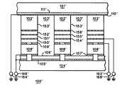
次に図7を参照すると、本発明による平面画像表示装置100の実施例の部分的側面概略図が示されている。実質的に光学的に透明な目視スクリーン構造体は、透明スクリーン101を含み、その上に陰極ルミネセンス物質層のような物質のエネルギ変換層111と導電陽極層110とが付着されている。この具体的実施例では、導電陽極層110上に間空(interspace)絶縁層102を配置する。間空絶縁層には、これを貫通する間空開口103が規定されており、この開口が間空領域を規定する。間空開口は全体的に円形の断面で形成され、間空絶縁層102によって包囲されている。
【0029】
複数の電子エミッタを電子放出基板104によって規定する。この電子放出基板104には、導電層105と、電子を放出する電子放出物質層106とが配置されている。導電接触層107を電子放出物質層106の表面上に配置し、それを貫通する開口を規定する。基板絶縁層108を接触層107上に配置し、接触層107を貫通する開口と同一の広がりを有しかつ同軸状に整合された開口を規定する。導電ゲート層109を基板絶縁層108上に配置し、接触層107を貫通する開口と同一の広がりを有しかつ同軸状に整合され、ゲート層109を貫通する開口を規定する。層107,108,109を貫通する個々の開口は合体して連続放出開口142を形成する。図7に示す実施例では、放出開口142が間空開口103の延長上にあり、間空開口103と実質的に一致するように、電子エミッタ140の導電ゲート層107を間空絶縁層102上に配置する。また、絶縁空間143が導電ゲート層109を部分的に分離することにより、導電ゲート層109を全体的にリング状の部分に分割し、各リング状部分が基板開口142の円周を実質的に囲むようにする。同様に、絶縁空間144によって層105,106,107を別個のリングに分離する。個々の電子エミッタを制御するために、種々のリング状部分の行または列を電気的に接続する。
【0030】
再び図7を参照すると、多数の電気ポテンシャル源162,164,166が図示されており、各々画像表示装置の1つ以上の素子に動作可能に接続されている。この説明のために例としてのみあげれば、電気ポテンシャル源162,164,166の各々は、接地電位のような基準電位に動作可能に接続することができる。しかし、これは動作の限定を意味する訳ではない。第1電気ポテンシャル源162は、導電ゲート層109と基準電位との間に動作可能に接続される。第2電気ポテンシャル源164は、導電陽極110と基準電位との間に動作可能に接続される。第3電気ポテンシャル源166は、電子放出物質層106を挟持する導電層105/107と基準電位との間に動作可能に接続される。
【0031】
上述の画像表示装置の動作の間、電子放出物質層106から放出される電子は、基板開口142および間空開口103の領域を横切り、陽極ルミネセンス層111に入射し、ここで電子が光子の放出を励起する。電気ポテンシャル源162は電気ポテンシャル源166と共に、電子の放出を制御するように機能する。電気ポテンシャル源164は、引力ポテンシャル(attractive potential)を発生して、間空開口103内に必要十分な電界を形成すると共に、放出された電子を捕獲する。画素アレイの所望部分に電気ポテンシャル源162,166を選択的に印加し、電子放出物質層106の連携する部分からの電子放出を制御可能とする。このように電子放出を制御することによって、面板(faceplate)101を通じて観察可能な所望の画像または複数の画像を得ることができる。
【0032】
本発明による平面画像表示装置100’の別の実施例の部分的側面概略図を図8に示す。図8では、図7において既に記載した構造には同様の参照番号を付け、全ての番号にダッシュを付加して、異なる実施例であることを示す。図8に詳細に示されているように、間空絶縁層102’は、積層された複数の絶縁層150’−153’から成り、これらの内いくつかの表面には、例としてのみあげれば、モリブデン、アルミニウム、チタン、ニッケル、またはタングステンのような導電層154’−156’がそれぞれ配置されている。したがって、個々の導電層154’−156’は、隣接する絶縁層150’−153’間に挟持されている。図8は4層の絶縁層を含み、その間に3層の導電層が挟持されているが、これ以下または以上のかかる導電層および/または絶縁層を用いて間空絶縁層102を実現することは予測できる。更に、絶縁層150’−153’のいくつかまたは全ては、導電層をその上に配置せずに形成することも予測できる。
【0033】
また、図8には、導電層、ここでは代表例として導電層154’と基準電位との間に動作可能に接続された、電圧源のような電気ポテンシャル源168’も示されている。電気ポテンシャル源168’は、間空開口103’内の電界に所望の変更を加え、エネルギ変換層111’に移動中の放出電子の軌道に影響を与えるように選択される。望ましければ、図示していない他の電気ポテンシャル源を、他の導電層155’,156’において同様に用いることもできる。
【0034】
次に図9を参照すると、本発明による電界放出素子32’に組み込まれる平面冷陰極電子エミッタ30’の更に他の実施例の部分的側面概略図が示されている。図9の構造は図3の構造に類似しており、同様の構成要素は同様の番号で表し、全ての番号にダッシュを付けることによって異なる実施例であることを示す。エミッタ30’は基板33’を含み、その表面上に低仕事関数物質層34’が配置されている。先に説明したように、層34’は、基板上に金属および/または安定物質およびダイアモンド等の複数の層を配することによって、形成することができる。
【0035】
導電接触層35’を層34’の表面上に配置する。接触層35’をパターニングして、それを貫通する開口37’を規定する。絶縁層38’を層35’上に配置し、それを貫通する開口39’を規定する。導電層40’を絶縁層38’上に配置し、電界放出素子32’の抽出ゲートを形成する。導電層40’をパターニングして、それを貫通する開口41’を規定する。層35’を貫通する開口37’、層38’を貫通する開口39’、および層40’を貫通する開口41’は実質的に同一の広がりを有し、周囲を整合して1つの連続開口を形成する。
【0036】
図9には開口37’,39’,41’の一方の縁しか示されていないが、他方の縁も「遠くに(far away)」存在するので、互いの電界分布を変えることはない。開口37’,39’,41’は大きな円形断面を有してもよいが、これらを細長チャンネル等としてもよい。事実上分離している開口37’,39’,41’の縁によって、比較的大きな形成(例えば、リソグラフィ/パターニングによる)を可能とすると共に、構造の製造を比較的容易にする。
【0037】
光学的に透明な目視スクリーン構造体42’は透明スクリーン43’を含み、その上に、陰極ルミネセンス物質層のような物質層44’と透明導電陽極層45’とが形成されている。本実施例では、層45’を透明スクリーン43’の表面上に配し、陰極ルミネセンス物質層44’を層45’の表面上に配することにより、スクリーン・バイアスの低下が可能となる。
【0038】
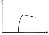
図9の構造に対する電界分布のシミュレーションを図10のグラフに示す。ここでは、垂直方向空間電界強度εと図9の構造における位置Pとの関係をプロットした。層34’の表面における電界分布によって、層40’(ゲート)の縁から遠いところで電子放出が生じる。軌道シミュレーションが示すのは、軌道は分散する、即ち合焦しないが、放出電子はゲートには達しない(miss)ということである。これに類似する実施例において放出電子を合焦するには、例えば、図8に示した構造に似た構造では、1層以上の導電層154’−156’を利用すればよい。
【0039】
以上、電子放出制御にパターニングされた金属を用いる、新たな改良された冷陰極電子エミッタが開示された。この新たな改良された冷陰極電子エミッタの新規な構造のために、周囲の誘電体への電子注入は減少または解消され、抽出電極電流は大幅に低減される。また、周囲の誘電体への電子注入を減少することによって、誘電体即ち素子のブレークダウンを大幅に低下させ、素子の信頼性を格段に向上させることになる。また、前記新たな改良された冷陰極電子エミッタの新規な構造は、動作特性および効率も向上させるものである。先の利点に加えて、前記新たな改良された冷陰極電子エミッタは、遠隔に配置された陽極において電子ビームを自動的に合焦する機能を組み込むことにより、表示装置等におけるエミッタの使用を改善することができる。結果的に、電子放出層と陰極ルミネセンス層との間に別個の支持用スペーサを用いない、構造的に堅牢(sound)な画像表示装置が開示された。
【図面の簡単な説明】
【図1】平面電界放出表示装置の実施例を表わす部分的側面概略図。
【図2】図1の構造における空間電界強度対位置の関係を示すグラフ。
【図3】本発明による平面電界放出表示装置の一実施例を表わす部分的側面概略図。
【図4】図3の構造における空間電界強度対位置の関係を示すグラフ。
【図5】図3の構造の断面の半分をコンピュータ・シミュレーションで簡略化して示すグラフ。
【図6】本発明による平面電界放出表示装置の他の実施例を表わす部分的側面概略図。
【図7】本発明による平面電界放出表示装置を縮小し大幅に簡素化して示す部分的側面概略図。
【図8】本発明による他の平面電界放出表示装置を縮小し大幅に簡素化して示す部分的側面概略図。
【図9】本発明による平面電界放出表示装置の更に他の実施例を表わす部分的側面概略図。
【図10】図9の構造に対する電界強度のシミュレーション結果を示すグラフ。
【符号の説明】
10,30,30’ 平面冷陰極電子エミッタ
12,32,62 電界放出素子
13,33,33’,63 基板
14,34,34’,64 低仕事関数物質層
15,38,38’,68,150’−153’ 絶縁層
17,37,37’,39,39’,41,41’,55 開口
18,40,40’,52 導電層
20,42,42’ 目視スクリーン構造体
22,44,44’ 陰極ルミネセンス物質層
23,45,45’,110 導電陽極層
35,35’,65,107 導電接触層
40,70,105,154’−156’ 導電層
43,43’,73,101 透明スクリーン
50 トライオード型電界放出素子
53 誘電体層
54 ゲート層
71 連続開口
101 面板
102,102’ 間空絶縁層
103 間空開口
104 電子放出基板
106 電子放出物質層
108 基板絶縁層
109 導電ゲート層
111 エネルギ変換層
140 電子エミッタ
142 連続放出開口
143 絶縁空間
162,164,166,168’ 電気ポテンシャル源[0001]
[Industrial application fields]
The present invention relates generally to cold cathode emission devices, and more particularly to electron emitters using diamond materials and similar emitters using low work function materials. .
[0002]
[Prior art]
Cold cathode electron emitters primarily include field emission devices, which are originally very sharp tips in order to increase the electric field at the tip surface and sufficiently draw off or emit electrons. Was necessary. In general, the extraction electrode is formed in a plane including the tip, and is disposed so as to completely surround the tip and provide an extraction potential between the tip and the extraction electrode. A major problem with these devices is that it is difficult to produce very sharp tips. Furthermore, once the chip is manufactured, the chip tends to degrade, i.e. lose particles, as the field emission device is operated.
[0003]
In order to solve these problems, there is a movement to use a low work function material for the emitter. As in the case of using a diamond emitter, in some cases, the emitter can be made to have a substantially planar structure while ensuring the amount of electron emission required by applying a reasonable potential. An example of such a structure is disclosed in US Pat. No. 5,283,501 entitled “Electron Device Employing a Low / Negative Electron Affinity Electron Source” and assigned to the same assignee as the present application.
[0004]
[Problems to be solved by the invention]
Even in these low work function elements, there is a problem that the extraction grid current is too much. When using a sharp tip, the emission is automatically done in the center of the emitter so that it can be focused before the electron stream hits the anode / screen. When using a planar emitter, electrons can be emitted from its surface anywhere in the electric field, so that most of the emitted electrons flow directly to the extraction electrode. When a current flows through the extraction electrode, the efficiency and operating characteristics of the element are greatly reduced.
[0005]
Accordingly, there is a need for a planar cold cathode emitter that overcomes at least some of the deficiencies of the prior art described above.
[0006]
One of the objects of the present invention is to provide a new and improved cold cathode electron emitter using a patterned metal for electron emission control.
[0007]
It is another object of the present invention to provide a new and improved cold cathode electron emitter which significantly reduces the extraction electrode current.
[0008]
Yet another object of the present invention is to provide a new and improved cold cathode electron emitter which reduces dielectric and thus device breakdown.
[0009]
Yet another object of the present invention is to provide a new and improved cold cathode electron emitter which reduces or eliminates electron injection into the surrounding dielectric.
[0010]
Yet another object of the present invention is to provide a new and improved cold cathode electron emitter with improved operating characteristics and efficiency.
[0011]
[Means for Solving the Problems]
The solution to the above and other problems, and the realization of the above and other objects, includes a substrate having a relatively planar surface and a low work function electron emitting material supported on the substrate surface and emitting electrons. Achieved by a planar cold cathode electron emitter. A contact conductive layer is disposed on the electron emissive material layer and defines an opening therethrough. An insulating layer is disposed over the contact conductive layer and defines an opening that is substantially on the extension of the contact conductive layer opening and is peripherally aligned. Further, a conductive gate layer is disposed on the insulating layer. The contact conductive layer forms a field potential such that emission occurs substantially in the center of the opening.
[0012]
【Example】
Referring now to FIG. 1, a partial side schematic diagram illustrating an embodiment of a planar cold
[0013]
When a sufficient positive voltage is applied to the
[0014]
Computer analysis of triode elements shows that the emission process is at least exponentially thermoionic and approximates Fowler-Nordheim. This is more steep than a single exponential in dependence on the surface electric field. Therefore, a small change in the spatial electric field strength characteristics along the surface of the
[0015]
In the structure of FIG. 1 in which the diameter D of the
[0016]
Another problem with the structure of FIG. 1 is that when
[0017]
Referring now to FIG. 3, a partial side schematic view of an embodiment of a planar cold
[0018]
A
[0019]
The optically transparent
[0020]
In the specific structure of FIG. 3, as shown in FIG. 4 as a whole, when the diameter of the
[0021]
In a specific embodiment of the invention,
[0022]
By changing the thickness of the
[0023]
Referring to FIG. 5, a half-sectional view simulating a triode type field emission device 50 (similar to the
[0024]
Another feature of the
[0025]
Another feature of the
[0026]
Referring now to FIG. 6, there is shown a partial side schematic view of another embodiment of a planar cold
[0027]
[0028]
Referring now to FIG. 7, there is shown a partial side schematic diagram of an embodiment of a flat
[0029]
A plurality of electron emitters are defined by the
[0030]
Referring again to FIG. 7, a number of electrical
[0031]
During the operation of the image display device described above, electrons emitted from the electron-emitting
[0032]
A partial side schematic view of another embodiment of a flat image display device 100 'according to the present invention is shown in FIG. In FIG. 8, the structures already described in FIG. 7 are given the same reference numbers, and dashes are added to all the numbers to indicate different embodiments. As shown in detail in FIG. 8, the interstitial insulating
[0033]
Also shown in FIG. 8 is an electrical
[0034]
Referring now to FIG. 9, there is shown a partial side schematic view of yet another embodiment of a planar cold cathode electron emitter 30 'incorporated into a field emission device 32' according to the present invention. The structure of FIG. 9 is similar to the structure of FIG. 3, like components are indicated by like numbers, and all numbers are marked with a dash to indicate a different embodiment. The emitter 30 'includes a substrate 33' on which a low work function material layer 34 'is disposed. As explained above, layer 34 'can be formed by placing multiple layers of metals and / or stabilizers and diamonds on the substrate.
[0035]
A conductive contact layer 35 'is disposed on the surface of layer 34'. Contact layer 35 'is patterned to define an opening 37' therethrough. An insulating layer 38 'is disposed on layer 35' and defines an opening 39 'extending therethrough. Conductive layer 40 'is disposed on insulating layer 38' to form an extraction gate for field emission device 32 '. The
[0036]
FIG. 9 shows only one edge of the
[0037]
The optically transparent viewing screen structure 42 'includes a transparent screen 43' on which a material layer 44 'such as a cathodoluminescent material layer and a transparent conductive anode layer 45' are formed. In this embodiment, the screen bias can be reduced by disposing the layer 45 'on the surface of the transparent screen 43' and disposing the cathodoluminescent material layer 44 'on the surface of the layer 45'.
[0038]
A simulation of the electric field distribution for the structure of FIG. 9 is shown in the graph of FIG. Here, the relationship between the vertical space electric field strength ε and the position P in the structure of FIG. 9 is plotted. Due to the electric field distribution on the surface of layer 34 ', electron emission occurs far from the edge of layer 40' (gate). The trajectory simulation shows that the trajectory is dispersed, i.e., not in focus, but the emitted electrons miss the gate. To focus the emitted electrons in an embodiment similar to this, for example, in a structure similar to the structure shown in FIG. 8, one or more
[0039]
Thus, a new and improved cold cathode electron emitter using a patterned metal for electron emission control has been disclosed. Due to the new structure of this new and improved cold cathode electron emitter, electron injection into the surrounding dielectric is reduced or eliminated and the extraction electrode current is greatly reduced. Also, by reducing the electron injection into the surrounding dielectric, the breakdown of the dielectric, i.e., the device, is greatly reduced, and the reliability of the device is significantly improved. The new improved cold cathode electron emitter structure also improves operating characteristics and efficiency. In addition to the previous advantages, the new and improved cold cathode electron emitter improves the use of the emitter in displays and the like by incorporating the ability to automatically focus the electron beam at a remotely located anode. can do. As a result, a structurally sound image display device has been disclosed that does not use a separate support spacer between the electron emitting layer and the cathodoluminescent layer.
[Brief description of the drawings]
FIG. 1 is a partial schematic side view illustrating an embodiment of a planar field emission display.
FIG. 2 is a graph showing the relationship between spatial electric field strength and position in the structure of FIG.
FIG. 3 is a partial schematic side view showing an embodiment of a flat field emission display device according to the present invention.
4 is a graph showing the relationship between spatial electric field strength and position in the structure of FIG. 3;
5 is a graph showing half of the cross section of the structure of FIG. 3 in a simplified manner by computer simulation.
FIG. 6 is a partial side schematic view showing another embodiment of a flat field emission display device according to the present invention.
FIG. 7 is a partial schematic side view showing a planar field emission display device according to the present invention in a reduced scale and greatly simplified.
FIG. 8 is a partial side schematic view showing another flat field emission display device according to the present invention in a reduced scale and greatly simplified.
FIG. 9 is a partial side schematic view showing still another embodiment of a flat field emission display device according to the present invention.
10 is a graph showing a simulation result of electric field strength for the structure of FIG. 9;
[Explanation of symbols]
10, 30, 30 'planar cold cathode electron emitter
12, 32, 62 field emission device
13, 33, 33 ', 63 substrate
14, 34, 34 ', 64 Low work function material layer
15, 38, 38 ', 68, 150'-153' insulating layer
17, 37, 37 ', 39, 39', 41, 41 ', 55 opening
18, 40, 40 ', 52 Conductive layer
20, 42, 42 'visual screen structure
22, 44, 44 'cathodoluminescent material layer
23, 45, 45 ', 110 Conductive anode layer
35, 35 ', 65, 107 conductive contact layer
40, 70, 105, 154'-156 'conductive layer
43, 43 ', 73, 101 Transparent screen
50 Triode field emission devices
53 Dielectric layer
54 Gate layer
71 Continuous opening
101 face plate
102,102 'space insulation layer
103 gap opening
104 Electron emission substrate
106 Electron emitting material layer
108 Substrate insulation layer
109 Conductive gate layer
111 Energy Conversion Layer
140 electron emitter
142 Continuous discharge opening
143 Insulation space
162, 164, 166, 168 'Electric potential source
Claims (3)
Translated fromJapanese比較的平坦な表面を有する基板(33);
前記基板上に支持され、電子を放出するための比較的平坦な表面を有する電子放出物質層(34);
前記電子放出物質層(34)上に配置され、開口(37)が規定された接触導電層(35);
前記接触導電層(35)上に配置され、前記接触導電層(35)内の前記開口(37)と実質的に周囲が整合された開口(39)が規定された絶縁層(38);および
前記絶縁層(38)上に配置されかつ前記接触導電層(35)および前記絶縁層(38)の前記開口(37,39)と実質的に周囲が整合された開口(41)が規定された導電ゲート層(40);
を具備することを特徴とする平面冷陰極電子エミッタ(30)。A planar cold cathode electron emitter (30) comprising:
A substrate (33) havinga relatively flat surface;
An electron emissive material layer (34)supported on the substrate and having a relatively flat surface for emitting electrons;
A contact conductive layer (35) disposedon the electron emissive material layer (34) and having an opening (37) defined;
An insulating layer (38) defined over said contact conductive layer (35) and having an opening (39) substantially perimeter aligned with said opening (37) in said contact conductive layer (35); andAn opening (41) is defined that is disposed on the insulating layer (38) and substantially peripherally aligned with the opening (37, 39) of the contact conductive layer (35) and the insulating layer (38). A conductive gate layer (40);
Characterized by comprising a flat cold cathode electron emitter (30).
電子エミッタ(30)であって、
電子を放出するための比較的平坦な表面を有する電子放出物質層(34)、
前記電子放出物質層(34)上に配置され、開口(37)が規定された導電接触層(35)、
前記導電接触層(35)の上側に位置する関係で配置され、実質的に前記接触導電層の開口と同一の広がりを有しかつ前記開口と周囲が整合された開口(39)が規定された絶縁層(38)、および
前記絶縁層(38)上に配置される導電ゲート層(40)であって、前記導電層および前記絶縁層における前記開口と実質的に同一の広がりを有しかつ前記開口と周囲が整合された開口(41)が規定された導電ゲート層(40)、
を含む前記電子エミッタ(30);ならびに
前記電子エミッタ(30)と離間された関係で配置され、主面を有し、透明面板(43)と該透明面板(43)に形成された陰極ルミネセンス物質層(44)とを含む、光学的に透明な面板構造体(42)であって、前記光学的に透明な面板構造体(42)の主面は前記導電接触層(35)と前記絶縁層(38)と前記導電ゲート層(40)とを貫通して規定された開口(37,39,41)の上側に位置し、前記電子放出物質層(34)から放出された電子は前記導電接触層(35)によって前記光学的に透明な面板構造体(42)の前記主面上に集束される前記面板構造体;
を具備することを特徴とする電界放出素子。A field emission device (32) comprising:
An electron emitter (30),
An electron emitter layer (34)having a relatively flat surface for emitting electrons;
A conductive contact layer (35) disposed on the electron emissive material layer (34) and having an opening (37) defined;
An opening (39) is defined which is arranged in a relationship located above the conductive contact layer (35), has substantially the same extent as the opening of the contact conductive layer and is aligned with the opening. An insulating layer (38), and
A conductive gate layer (40) disposed on said insulating layer (38), having substantially the same extent as said opening in said conductive layer and said insulating layer, and said opening and surroundings being aligned; A conductive gate layer (40) in which an opening (41) is defined;
Said electron emitter (30) comprising:
An optical element disposed in a spaced relationship with the electron emitter (30), having a main surface, comprising a transparent face plate (43) and a cathodoluminescent material layer (44) formed on the transparent face plate (43). Transparent face plate structure (42), wherein the main surface of the optically transparent face plate structure (42) includes the conductive contact layer (35), the insulating layer (38), and the conductive gate layer ( 40), the electrons emitted from the electron-emitting material layer (34) are optically emitted by the conductive contact layer (35) and located above the defined openings (37, 39, 41). The face plate structure focused on the main surface of the transparent face plate structure (42);
A field emission devicecomprising:
主面を有し、透明面板(101)、陰極ルミネセンス物質(111)および導電陽極(110)を含む光学的に透明な面板構造体;
前記面板構造体の前記主面上に配置され、開口(103)が規定され、該開口(103)が間空領域を規定する、間空絶縁層(102);
電子エミッタ(140)であって、
電子を放出するための比較的平坦な表面を有する電子放出物質層(106)、
前記電子放出物質層(106)上に配置された導電接触層(107)、
前記導電接触層(107)の上側に位置付けられる関係で配置された絶縁層(108)、
前記絶縁層(108)上に配置された導電ゲート層(109)、
を含み、前記電子エミッタは、前記導電接触層(107)、前記絶縁層(108)、および前記導電ゲート層(109)を貫通して規定された少なくとも1つの開口(142)を有する電子エミッタ(140);
を具備し、
前記電子エミッタ(140)は、前記導電ゲート層(109)が前記導電陽極(110)と前記電子放出層(106)との間に介在するように、前記間空絶縁層(102)上に配置され、
前記電子エミッタ(140)を貫通して規定された開口(142)が前記間空絶縁層(102)を貫通して規定された開口(103)と実質的に周囲が整合されるように配置され、かつ
前記電子放出物質層(106)によって放出された電子が前記導電接触層(107)によって前記導電陽極(110)上に集束されて、前記陰極ルミネセンス物質(111)からの光子の放出を励起する、
ことを特徴とする電界放出素子。A field emission device (100) comprising :
An optically transparent faceplate structure having a major face and comprising a transparent faceplate (101), a cathodoluminescent material (111) and a conductive anode (110);
A space insulating layer (102) disposed on the major surface of the face plate structure, defining an opening (103), the opening (103) defining a space region;
An electron emitter (140),
An electron emissive material layer (106)having a relatively flat surface for emitting electrons;
A conductive contact layer (107) disposed on the electron emissive material layer (106);
An insulating layer (108) disposed in a relationship positionedabove the conductive contact layer (107 );
Aconductive gate layer (109) disposed on the insulating layer (108);
The electron emitter having at least one opening (142) defined through the conductive contact layer (107), the insulating layer (108), and the conductive gate layer (109) 140);
Comprising
The electron emitter (140) isdisposed on the space insulating layer (102) such that the conductive gate layer (109) is interposed between the conductive anode (110) and the electron emission layer (106).And
The opening (142) defined through the electron emitter (140) isarranged to be substantially aligned with the opening (103) defined through the space insulating layer (102).And the electrons emitted by the electron-emitting material layer (106) arefocused on the conductive anode (110) by the conductive contact layer (107) to release photons from the cathodoluminescent material (111). Excited,
A field emission device characterized bythat .
Applications Claiming Priority (2)
| Application Number | Priority Date | Filing Date | Title |
|---|---|---|---|
| US08/251,415US5473218A (en) | 1994-05-31 | 1994-05-31 | Diamond cold cathode using patterned metal for electron emission control |
| US251415 | 2002-09-20 |
Publications (2)
| Publication Number | Publication Date |
|---|---|
| JPH0855564A JPH0855564A (en) | 1996-02-27 |
| JP3734530B2true JP3734530B2 (en) | 2006-01-11 |
Family
ID=22951873
Family Applications (1)
| Application Number | Title | Priority Date | Filing Date |
|---|---|---|---|
| JP15115795AExpired - Fee RelatedJP3734530B2 (en) | 1994-05-31 | 1995-05-26 | Planar cold cathode electron emitter and field emission device |
Country Status (4)
| Country | Link |
|---|---|
| US (1) | US5473218A (en) |
| EP (1) | EP0685869B1 (en) |
| JP (1) | JP3734530B2 (en) |
| TW (1) | TW267234B (en) |
Families Citing this family (48)
| Publication number | Priority date | Publication date | Assignee | Title |
|---|---|---|---|---|
| CA2172803A1 (en) | 1993-11-04 | 1995-05-11 | Nalin Kumar | Methods for fabricating flat panel display systems and components |
| FR2726688B1 (en)* | 1994-11-08 | 1996-12-06 | Commissariat Energie Atomique | FIELD-EFFECT ELECTRON SOURCE AND MANUFACTURING METHOD THEREOF, APPLICATION TO CATHODOLUMINESCENCE VISUALIZATION DEVICES |
| US5598056A (en)* | 1995-01-31 | 1997-01-28 | Lucent Technologies Inc. | Multilayer pillar structure for improved field emission devices |
| KR100343214B1 (en)* | 1995-03-28 | 2002-11-13 | 삼성에스디아이 주식회사 | manufacturing method of field emission device |
| RU2089001C1 (en)* | 1996-02-29 | 1997-08-27 | Закрытое акционерное общество "Техно-ТМ" | Source of electrons and method of its manufacture |
| US5837331A (en)* | 1996-03-13 | 1998-11-17 | Motorola, Inc. | Amorphous multi-layered structure and method of making the same |
| US6504311B1 (en)* | 1996-03-25 | 2003-01-07 | Si Diamond Technology, Inc. | Cold-cathode cathodoluminescent lamp |
| US5729094A (en)* | 1996-04-15 | 1998-03-17 | Massachusetts Institute Of Technology | Energetic-electron emitters |
| US5880559A (en)* | 1996-06-01 | 1999-03-09 | Smiths Industries Public Limited Company | Electrodes and lamps |
| CN1119829C (en)* | 1996-09-17 | 2003-08-27 | 浜松光子学株式会社 | Photoelectric cathode and electron tube equiped with same |
| RU2126187C1 (en)* | 1996-11-01 | 1999-02-10 | Закрытое акционерное общество "Техно-ТМ" | Flat device for displaying information |
| US5696385A (en)* | 1996-12-13 | 1997-12-09 | Motorola | Field emission device having reduced row-to-column leakage |
| GB2322471A (en)* | 1997-02-24 | 1998-08-26 | Ibm | Self stabilising cathode |
| US6194838B1 (en) | 1997-02-24 | 2001-02-27 | International Business Machines Corporation | Self stabilizing non-thermionic source for flat panel CRT displays |
| US6215243B1 (en) | 1997-05-06 | 2001-04-10 | St. Clair Intellectual Property Consultants, Inc. | Radioactive cathode emitter for use in field emission display devices |
| US6323594B1 (en) | 1997-05-06 | 2001-11-27 | St. Clair Intellectual Property Consultants, Inc. | Electron amplification channel structure for use in field emission display devices |
| US5982082A (en)* | 1997-05-06 | 1999-11-09 | St. Clair Intellectual Property Consultants, Inc. | Field emission display devices |
| KR100477722B1 (en)* | 1997-08-19 | 2005-10-06 | 삼성에스디아이 주식회사 | Surface Emission Field Emission Display |
| KR100477727B1 (en)* | 1997-08-29 | 2005-06-07 | 삼성에스디아이 주식회사 | Field emission display device and manufacturing method thereof |
| GB2330687B (en)* | 1997-10-22 | 1999-09-29 | Printable Field Emitters Ltd | Field emission devices |
| US5949185A (en)* | 1997-10-22 | 1999-09-07 | St. Clair Intellectual Property Consultants, Inc. | Field emission display devices |
| US6441543B1 (en)* | 1998-01-30 | 2002-08-27 | Si Diamond Technology, Inc. | Flat CRT display that includes a focus electrode as well as multiple anode and deflector electrodes |
| US6400069B1 (en) | 1998-07-22 | 2002-06-04 | Robert Espinosa | E-M wave generation using cold electron emission |
| US6204597B1 (en) | 1999-02-05 | 2001-03-20 | Motorola, Inc. | Field emission device having dielectric focusing layers |
| RU2170471C1 (en)* | 1999-11-30 | 2001-07-10 | Научно-исследовательский институт "Волга" | Cathodic fluorescent screen |
| JP4750920B2 (en)* | 2000-03-24 | 2011-08-17 | 住友電気工業株式会社 | Electron emitter |
| RU2176835C1 (en)* | 2000-06-09 | 2001-12-10 | Логинов Александр Александрович | Vacuum fluorescent display |
| JP2002063864A (en)* | 2000-08-21 | 2002-02-28 | Ise Electronics Corp | Fluorescent display tube |
| KR100762590B1 (en)* | 2001-01-11 | 2007-10-01 | 엘지전자 주식회사 | Field emission type display device using carbon nanotube and manufacturing method thereof |
| US6781146B2 (en)* | 2001-04-30 | 2004-08-24 | Hewlett-Packard Development Company, L.P. | Annealed tunneling emitter |
| US6882100B2 (en)* | 2001-04-30 | 2005-04-19 | Hewlett-Packard Development Company, L.P. | Dielectric light device |
| US6753544B2 (en)* | 2001-04-30 | 2004-06-22 | Hewlett-Packard Development Company, L.P. | Silicon-based dielectric tunneling emitter |
| US6911768B2 (en) | 2001-04-30 | 2005-06-28 | Hewlett-Packard Development Company, L.P. | Tunneling emitter with nanohole openings |
| JP2003086080A (en)* | 2001-09-14 | 2003-03-20 | Sony Corp | Cold cathode field emission device and cold cathode field emission display |
| US6703252B2 (en) | 2002-01-31 | 2004-03-09 | Hewlett-Packard Development Company, L.P. | Method of manufacturing an emitter |
| JP3745348B2 (en)* | 2003-06-16 | 2006-02-15 | キヤノン株式会社 | Electron emitting device, electron source, and manufacturing method of image display device |
| US20050104506A1 (en)* | 2003-11-18 | 2005-05-19 | Youh Meng-Jey | Triode Field Emission Cold Cathode Devices with Random Distribution and Method |
| JP2006079873A (en)* | 2004-09-08 | 2006-03-23 | National Institute For Materials Science | Deep UV solid state light emitting device |
| US7429820B2 (en)* | 2004-12-07 | 2008-09-30 | Motorola, Inc. | Field emission display with electron trajectory field shaping |
| JP2007214032A (en)* | 2006-02-10 | 2007-08-23 | Canon Inc | Electron emitting device, electron source, and manufacturing method of image display device |
| JP2007294126A (en) | 2006-04-21 | 2007-11-08 | Canon Inc | Electron emitting device, electron source, image display apparatus, and method for manufacturing electron emitting device |
| JP2008282607A (en)* | 2007-05-09 | 2008-11-20 | Canon Inc | Electron-emitting device, electron source, image display device, and method for manufacturing electron-emitting device |
| JP2009110755A (en)* | 2007-10-29 | 2009-05-21 | Canon Inc | Electron emitting device, electron source, image display device, and method of manufacturing electron emitting device |
| RU2378733C1 (en)* | 2008-04-16 | 2010-01-10 | ФЕДЕРАЛЬНОЕ ГОСУДАРСТВЕННОЕ УНИТАРНОЕ ПРЕДПРИЯТИЕ "Научно-исследовательский институт "ВОЛГА" (ФГУП "НИИ "ВОЛГА") | Matrix cathodoluminescent screen |
| US8922107B2 (en) | 2011-05-10 | 2014-12-30 | Brookhaven Science Associates, Llc | Vacuum encapsulated hermetically sealed diamond amplified cathode capsule and method for making same |
| US9224570B2 (en) | 2012-05-18 | 2015-12-29 | Brookhaven Science Associates, Llc | Vacuum encapsulated, high temperature diamond amplified cathode capsule and method for making same |
| US9916746B2 (en) | 2013-03-15 | 2018-03-13 | August Home, Inc. | Security system coupled to a door lock system |
| EP4337475A4 (en)* | 2021-06-04 | 2024-08-14 | Orta Dogu Teknik Universitesi | REDUCING ELECTRICAL CROSSTALK FOR A CAPACITIVE MICROMACHINED ULTRASONIC TRANSDUCER ARRANGEMENT |
Family Cites Families (4)
| Publication number | Priority date | Publication date | Assignee | Title |
|---|---|---|---|---|
| US3735186A (en)* | 1971-03-10 | 1973-05-22 | Philips Corp | Field emission cathode |
| FR2623013A1 (en)* | 1987-11-06 | 1989-05-12 | Commissariat Energie Atomique | ELECTRO SOURCE WITH EMISSIVE MICROPOINT CATHODES AND FIELD EMISSION-INDUCED CATHODOLUMINESCENCE VISUALIZATION DEVICE USING THE SOURCE |
| CA2070478A1 (en)* | 1991-06-27 | 1992-12-28 | Wolfgang M. Feist | Fabrication method for field emission arrays |
| US5382812A (en)* | 1993-04-14 | 1995-01-17 | Kobe Development Corporation | Diamond and II-VI heterojunction semiconductor light emitting device |
- 1994
- 1994-05-31USUS08/251,415patent/US5473218A/ennot_activeExpired - Fee Related
- 1995
- 1995-04-19TWTW084103854Apatent/TW267234B/zhactive
- 1995-05-26JPJP15115795Apatent/JP3734530B2/ennot_activeExpired - Fee Related
- 1995-05-26EPEP95108078Apatent/EP0685869B1/ennot_activeExpired - Lifetime
Also Published As
| Publication number | Publication date |
|---|---|
| US5473218A (en) | 1995-12-05 |
| EP0685869A1 (en) | 1995-12-06 |
| JPH0855564A (en) | 1996-02-27 |
| EP0685869B1 (en) | 1998-09-23 |
| TW267234B (en) | 1996-01-01 |
Similar Documents
| Publication | Publication Date | Title |
|---|---|---|
| JP3734530B2 (en) | Planar cold cathode electron emitter and field emission device | |
| JP3727894B2 (en) | Field emission electron source | |
| KR100523840B1 (en) | Field Emission Device | |
| JP2809129B2 (en) | Field emission cold cathode and display device using the same | |
| US7696680B2 (en) | Field emission device for high resolution display | |
| CA2172803A1 (en) | Methods for fabricating flat panel display systems and components | |
| US20050184647A1 (en) | Electron emission device | |
| US7315115B1 (en) | Light-emitting and electron-emitting devices having getter regions | |
| JP2731733B2 (en) | Field emission cold cathode and display device using the same | |
| KR100540144B1 (en) | Field emission device and field emission display device using the same | |
| US5920151A (en) | Structure and fabrication of electron-emitting device having focus coating contacted through underlying access conductor | |
| KR20060019846A (en) | Electron-emitting device | |
| JPWO2002061789A1 (en) | Electron emission device and field emission display | |
| US20050266766A1 (en) | Method for manufacturing carbon nanotube field emission display | |
| US7078863B2 (en) | Cold-cathode electron source and field-emission display | |
| US6013974A (en) | Electron-emitting device having focus coating that extends partway into focus openings | |
| US7348717B2 (en) | Triode type field emission display with high resolution | |
| CN100521056C (en) | Electron emission device | |
| US7498732B2 (en) | Electron emission device with a grid electrode and electron emission display having the same | |
| JP2005294262A (en) | Electron emission device and electron emission display device using the same | |
| JP3483972B2 (en) | Field emission cathode | |
| KR101049822B1 (en) | Electron-emitting device | |
| US7138760B2 (en) | Electron emission device and electron emission display having beam-focusing structure using insulating layer | |
| KR100903615B1 (en) | Spacer for Electron Emission Display and Electron Emission Display | |
| KR100322732B1 (en) | Horizontal field effect electron-emitting device and its manufacturing method |
Legal Events
| Date | Code | Title | Description |
|---|---|---|---|
| A977 | Report on retrieval | Free format text:JAPANESE INTERMEDIATE CODE: A971007 Effective date:20040709 | |
| A131 | Notification of reasons for refusal | Free format text:JAPANESE INTERMEDIATE CODE: A131 Effective date:20040810 | |
| A521 | Request for written amendment filed | Free format text:JAPANESE INTERMEDIATE CODE: A523 Effective date:20041110 | |
| TRDD | Decision of grant or rejection written | ||
| A01 | Written decision to grant a patent or to grant a registration (utility model) | Free format text:JAPANESE INTERMEDIATE CODE: A01 Effective date:20051004 | |
| A61 | First payment of annual fees (during grant procedure) | Free format text:JAPANESE INTERMEDIATE CODE: A61 Effective date:20051019 | |
| R150 | Certificate of patent or registration of utility model | Free format text:JAPANESE INTERMEDIATE CODE: R150 | |
| FPAY | Renewal fee payment (event date is renewal date of database) | Free format text:PAYMENT UNTIL: 20081028 Year of fee payment:3 | |
| FPAY | Renewal fee payment (event date is renewal date of database) | Free format text:PAYMENT UNTIL: 20091028 Year of fee payment:4 | |
| FPAY | Renewal fee payment (event date is renewal date of database) | Free format text:PAYMENT UNTIL: 20091028 Year of fee payment:4 | |
| RD03 | Notification of appointment of power of attorney | Free format text:JAPANESE INTERMEDIATE CODE: R3D03 | |
| LAPS | Cancellation because of no payment of annual fees |