JP3732702B2 - Image processing device - Google Patents
Image processing deviceDownload PDFInfo
- Publication number
- JP3732702B2 JP3732702B2JP2000023131AJP2000023131AJP3732702B2JP 3732702 B2JP3732702 B2JP 3732702B2JP 2000023131 AJP2000023131 AJP 2000023131AJP 2000023131 AJP2000023131 AJP 2000023131AJP 3732702 B2JP3732702 B2JP 3732702B2
- Authority
- JP
- Japan
- Prior art keywords
- image data
- image
- data
- unit
- line
- Prior art date
- Legal status (The legal status is an assumption and is not a legal conclusion. Google has not performed a legal analysis and makes no representation as to the accuracy of the status listed.)
- Expired - Fee Related
Links
Images


Classifications
- H—ELECTRICITY
- H04—ELECTRIC COMMUNICATION TECHNIQUE
- H04N—PICTORIAL COMMUNICATION, e.g. TELEVISION
- H04N1/00—Scanning, transmission or reproduction of documents or the like, e.g. facsimile transmission; Details thereof
- H04N1/32—Circuits or arrangements for control or supervision between transmitter and receiver or between image input and image output device, e.g. between a still-image camera and its memory or between a still-image camera and a printer device
- H04N1/32358—Circuits or arrangements for control or supervision between transmitter and receiver or between image input and image output device, e.g. between a still-image camera and its memory or between a still-image camera and a printer device using picture signal storage, e.g. at transmitter
- H—ELECTRICITY
- H04—ELECTRIC COMMUNICATION TECHNIQUE
- H04N—PICTORIAL COMMUNICATION, e.g. TELEVISION
- H04N1/00—Scanning, transmission or reproduction of documents or the like, e.g. facsimile transmission; Details thereof
- H04N1/40—Picture signal circuits
- H—ELECTRICITY
- H04—ELECTRIC COMMUNICATION TECHNIQUE
- H04N—PICTORIAL COMMUNICATION, e.g. TELEVISION
- H04N2201/00—Indexing scheme relating to scanning, transmission or reproduction of documents or the like, and to details thereof
- H04N2201/32—Circuits or arrangements for control or supervision between transmitter and receiver or between image input and image output device, e.g. between a still-image camera and its memory or between a still-image camera and a printer device
- H04N2201/3285—Circuits or arrangements for control or supervision between transmitter and receiver or between image input and image output device, e.g. between a still-image camera and its memory or between a still-image camera and a printer device using picture signal storage, e.g. at transmitter
- H04N2201/329—Storage of less than a complete document page or image frame
Landscapes
- Engineering & Computer Science (AREA)
- Multimedia (AREA)
- Signal Processing (AREA)
- Compression Of Band Width Or Redundancy In Fax (AREA)
- Image Processing (AREA)
Description
Translated fromJapanese【0001】
【発明の属する技術分野】
この発明は、画像処理装置、特に、ラインメモリーを用いて画像データを圧縮する処理もしくは伸張する処理をおこなう画像処理装置に関する。
【0002】
【従来の技術】
従来、アナログ複写機からディジタル化された画像データの処理をおこなうディジタル複写機が登場し、さらに、ディジタル複写機が複写機としての機能だけでなく、複写機の機能に加えて、ファクシミリの機能、プリンターの機能、スキャナーの機能等の各機能を複合したディジタル複合機が存在する。
【0003】
図15は、従来技術にかかるディジタル複合機のハードウエア構成の一例を示すブロック図である。図15に示すように、ディジタル複合機1500は、読取ユニット1501、画像処理ユニット1502、ビデオ制御部1503、書込ユニット1504の一連の各構成部、さらにはメモリー制御ユニット1505およびメモリー・モジュール1506によって形成される複写機を構成する部分(複写機部分)と、マザーボード1511を介して、追加的にファクシミリ制御ユニット1512、プリンター制御ユニット1513、スキャナー制御ユニット1514等のユニットが接続されることによって、ディジタル複合機としての各機能を実現していた。
【0004】
すなわち、上記一連の構成部による一つのシステム、具体的にはシステム・コントローラ1507、RAM1508およびROMによって一連の動作がコントロールされている複写機部分にファクシミリ制御ユニット1512、プリンター制御ユニット1513、スキャナー制御ユニット1514をアドオンすることにより、ディジタル複合機の機能を実現するものであった。
【0005】
また、図示は省略するが、上記各ユニットを複写機にアドオンするものではなく、複写機能部分、ファクシミリ機能部分、プリンター機能部分等をそれぞれユニット化して組み合わせ、これら各ユニットから入力する画像データを効率よく処理するディジタル複合機も案出されている。
【0006】
ディジタル複合機がマザーボードを介して機能ユニットをアドオンするものであっても、複写機に特化することなく各機能ユニットをつくり分けて組み合わせるものであっても、ディジタル複合機の多機能化にともない、画像データの転送制御はシステムのパフォーマンス向上の観点から非常に重要な要素となってくる。
【0007】
したがって従来では転送制御の観点、すなわち、各機能ユニット間による画像データの転送効率や、メモリー等の記憶部における記憶効率を考慮して、画像データは必要に応じて圧縮されていた。換言すると、画像データを圧縮することでディジタル複合機はそのパフォーマンスの向上を図っていた。
【0008】
ここで、画像データを圧縮する従来のデータ圧縮部について説明する。図16は、従来のデータ圧縮部の構成の一例を示すブロック図であり、図17は、その処理タイミング示す説明図である。
【0009】
図16において、データ圧縮部1601は、画像データを格納する格納部1602と、画像データを圧縮する圧縮器1603と、格納部1602および圧縮器1603を制御する制御部1604と、から構成される。格納部1602は、複数の1ポートFIFOメモリーFM1a、FM1b、FM2、FM3およびFM4から構成されるラインメモリー群1605と、画像データの出力先を切り替える出力切替器1606と、画像データの入力先をFIFOメモリーFM1aおよびFM1b間で切り替える入力切替器1607と、から構成される。
【0010】
なお、ここでは説明の簡単のために、圧縮器1603で圧縮する圧縮領域としては、図18に示すように主走査(画素)方向に4画素、副走査(ライン)方向に4ラインからなる1ライン4画素×4ラインの矩形領域とする。
【0011】
図17に示したように、画像データの圧縮については、まず、矩形領域の第1ラインの画像データをFIFOメモリーFM1aにライトする(書き込む)。つぎに、第2ラインの画像データをFIFOメモリーFM2に、第3ラインの画像データをFIFOメモリーFM3に、第4ラインの画像データをFIFOメモリーFM4に順次書き込む。この際の画像データの切り分け作業は、制御部1604の制御の下、出力切替器1606がおこなう。
【0012】
FIFOメモリーFM4に画像データを書き込んだ段階で、圧縮器1603で圧縮すべき4ラインがそろうので、つぎに、FIFOメモリーFM1a、FM2、FM3およびFM4に格納された第1ラインから第4ラインの画像データをリードし(読み出し)、圧縮器1603に送出する。この送出制御は、制御部1604がおこなう。圧縮器1603は、入力された4ライン分の画像データを圧縮し、圧縮された画像データを出力する。この圧縮された画像データは、メモリー制御ユニット1505を介してメモリー・モジュール1506に格納される。
【0013】
一方、第4ラインの画像データがFIFOメモリーFM4に書き込まれた後、つぎの矩形領域の最初のラインの画像データ(第5ラインの画像データ)が入力される。制御部1604は、メモリー使用の競合回避のため、この第5ラインの画像データをFIFOメモリーFM1bに書き込む制御をおこなう。
【0014】
その後第6ラインの画像データをFIFOメモリーFM2に、第7ラインのデータをFIFOメモリーFM3に、第8ラインの画像データをFIFOメモリーFM4に順次書き込む。
【0015】
制御部1604は、つぎの矩形領域の第9ラインの画像データをFIFOメモリー1aに書き込む制御をおこないつつ、FIFOメモリーFM1b、FM2、FM3およびFM4に格納された第5ラインから第8ラインの画像データを読み出し、圧縮器1603に送出する。この処理を繰り返すことにより、順次入力する一連の画像データを滞りなく圧縮することが可能となる。
【0016】
また、以上の例では、各FIFOメモリーは1ポートFIFOメモリーであるが、2ポートFIFOメモリーを用いることもできる。図19は、2ポートFIFOメモリーを一部に用いたデータ圧縮部の構成の一例を示した図であり、図20は、その処理タイミングを示す説明図である。データ圧縮部1901は、データ圧縮部1601のFIFOメモリーFM1a、FIFOメモリーFM1bおよび切替器1607を2ポートFIFOメモリーFMD1に置き換えた以外はデータ圧縮部1601の構成と同一であるので、その説明を省略する。
【0017】
図20に示したように、データ圧縮部1901の動作としては、FIFOメモリーFM4に第4ラインの画像データを書き込んだ後、FIFOメモリーFMD1、FM2、FM3およびFM4に格納された第1ラインから第4ラインまでの画像データを読み出し、圧縮器1903に送出する。この読み出し制御と同時にFIFOメモリーFMD1に、つぎの第5ラインの画像データを書き込む。
【0018】
同様に、第8ラインの画像データをFIFOメモリーFM4に格納後、第9ラインの画像データをFIFOメモリーFMD1に書き込みながら、FIFOメモリーFMD1、FM2、FM3およびFM4に格納された第5ラインから第8ラインまでの画像データを読み出し、圧縮器1903に送出する。
【0019】
このように、FIFOメモリーに一部2ポートFIFOメモリーを使用することにより、1本分の1ポートFIFOメモリーを削減することができ、かつ、順次入力する一連の画像データを滞りなく圧縮することが可能となる。
【0020】
一方、圧縮された画像データは必要に応じて伸張され、その後の処理がおこなわれる。特に、ディジタル複合機にあっては、その機能の多様性に基づいて、メモリー・モジュール1506に格納された、圧縮された画像データを伸張する必要が生ずる場合が多い。
【0021】
ここで、従来の画像データを伸張するデータ伸張部について説明する。図21は、従来のデータ伸張部の構成の一例を示すブロック図であり、図22は、その処理タイミングを示す説明図である。
【0022】
図21において、データ伸張部2101は、圧縮された画像データを入力する入力側格納部2102と、画像データを伸張する伸張器2103と、伸張したデータを格納する出力側格納部2104と、入力側格納部2102、伸張器2103および出力側格納部2104を制御する制御部2105と、から構成される。なお、ここでは、説明の簡単のために、1ライン4画素×4ラインからなる矩形領域の画像データごとに圧縮された画像データを伸張するものとする。
【0023】
入力側格納部2102は、圧縮された矩形領域の画像データを格納する2つの1ポートFIFOメモリーFMI1およびFMI2と、圧縮された矩形領域の画像データをFIFOメモリーFMI1およびFMI2のいずれに送出するかを切り替える出力切替器2106と、から構成される。
【0024】
出力側格納部2104は、3本の1ポートFIFOメモリーFM1、FM2およびFM3と、1本の2ポートFIFOメモリーFMD4とからなるメモリー群2107と、メモリー群2107から出力される画像データの入力先を切り替える入力切替器2108と、から構成される。
【0025】
図22に示したように、画像データの伸張については、まず、圧縮された矩形領域の画像データがFIFOメモリーFMI1に送出される。この圧縮された画像データは伸張器2103に送出され、第1ラインから第4ラインの4ライン分の画像データに一括して伸張される。伸張された第1ラインの画像データはFIFOメモリーFM1に、第2ラインの画像データはFIFOメモリーFM2に、第3ラインの画像データはFIFOメモリーFM3に、第4ラインの画像データはFIFOメモリーFMD4に書き込まれる。
【0026】
つぎに、ラインデータ出力同期信号(図示せず)に応じて、FIFOメモリーFM1、FM2、FM3およびFMD4に格納された第1から第4ラインの画像データを順次読み出し、所定の出力先に送出する。一方、FIFOメモリーFMI2に格納された第5から第8ラインの圧縮された画像データは伸張器2103において伸張され、FIFOメモリーFM1からFMD4に格納される。このときFIFOメモリーFMD4においては、第4ラインの読み出しと、第8ラインの書き込みとが同時におこなわれる様に制御する。このため、FIFOメモリーFMD4はリードとライトが並行して可能な2ポートFIFOメモリーとしている。
【0027】
このように、FIFOメモリーに一部2ポートFIFOメモリーを使用することで、データ圧縮部1901と同様に、1本分の1ポートFIFOメモリーを削減することができ、かつ、順次入力する一連の圧縮された画像データを伸張し、滞りなく連続した画像データを送出することが可能となる。
【0028】
以上説明したように、従来の画像処理装置(ディジタル複合機)では、システムのパフォーマンス向上の観点から画像データの転送制御の効率化が求められ、これを満たすために前後に適当なラインメモリーを配したデータ圧縮部やデータ伸張部が設けられていた。
【0029】
また、読み取り信号の画像処理、メモリーへの画像蓄積、複数機能の並行動作およびそれぞれの画像処理を最適化する『画像処理装置』(たとえば、特開平8−274986号公報)等が開示されており、各種の画像処理を一つの画像処理構成で実行できるものがあった。
【0030】
【発明が解決しようとする課題】
しかしながら、上記従来技術におけるディジタル複合機においては、つぎのような問題点があった。データ圧縮部もしくはデータ伸張部については、前述したごとく、圧縮器もしくは伸張器の前後に複数のラインメモリーを含んだ構成となっている。このラインメモリーに関しては、アドオンする機能ユニット、もしくは、組み合わせる機能ユニットの種類や性能によって、入力する画像データの容量が相違するため、1本のラインメモリーの容量をあらかじめ大きく設計し、また、その数も多く設計する必要がある。
【0031】
特に、各機能ユニットを組み合わせるディジタル複合機については、機能向上により、一部の機能ユニットが交換される場合もあり、このような場合にも対応するため、1本のラインメモリーの容量を大きく、また、その本数を多く設計する必要がある。
【0032】
たとえば、1画素8bitとして1ライン600dpi(dot per inch)で原稿を読み込む場合、A4サイズ長手方向で約8k(1k=1024)となるため、1ラインの画像データを格納するためには、8bit×8kワードのラインメモリーが必要となる。
【0033】
すなわち、従来技術にかかる画像処理装置(ディジタル複合機)では、ラインメモリーの本数を多く、かつ、当該メモリー1本の容量を大きくする必要があるため、回路規模が大きくなるという問題点があった。ここで、ラインメモリーに2ポートFIFOメモリーを用いることにより、1本分の1ポートラインメモリーを削減できるが(図19、図21参照)、この場合でも、1ポートFIFOメモリーと比較した場合にあっては、2ポートFIFOメモリーはまだ回路規模が大きいという問題点があった。
【0034】
さらに、各機能ユニットを組み合わせるディジタル複合機の場合には、ほかの機能ユニットとの組み合わせにおいて使用されるので、設計上できるだけ回路規模を小さくし、これによりデータ圧縮部もしくはデータ伸張部を含む機能ユニットの大きさをできるだけ小さくしたいという要請もある。
【0035】
この発明は、上述した従来技術による問題点を解消するため、回路規模の縮小化を図ることが可能な画像処理装置を提供することを目的とする。
【0036】
【課題を解決するための手段】
上述した課題を解決し、目的を達成するため、この発明にかかる画像処理装置は、1ラインをm画素とするnラインからなるm×n画素に画像データを区分けする区分け手段と、前記区分け手段により区分けされた画素の画像データを格納する格納手段と、前記区分け手段により区分けされた画素の画像データおよび前記格納手段により格納された画像データをそれぞれ所定の送出先に送出する制御をおこなう制御手段と、m×n画素の画像データを一括して圧縮する圧縮手段と、を備え、前記制御手段が、前記区分け手段により区分けされたm×n画素の画像データのうち(n−1)ライン分の画像データを前記格納手段に送出し、残りの1ライン分の画像データについては前記圧縮手段に直接送出するとともに、前記格納手段に格納されたm×(n−1)画素の画像データを前記圧縮手段に送出する制御をおこなうことを特徴とする。
【0037】
この発明によれば、格納手段により格納される画像データの容量を1ライン分削減することが可能となる。
【0038】
また、この発明にかかる画像処理装置は、上記発明において、前記格納手段が、(n−1)本のFIFOメモリーにより構成され、前記制御手段が、前記区分け手段により区分けされた画像データを各ラインごとに前記FIFOメモリーに送出する制御をおこなうことを特徴とする。
【0039】
この発明によれば、複数のFIFOメモリーを使用することにより簡便な制御方法を用いることができ、回路設計が容易になる。
【0040】
また、この発明にかかる画像処理装置は、圧縮されたm×n画素の画像データである圧縮データを一括して伸張する伸張手段と、前記伸張手段により伸張された画像データを格納する格納手段と、前記伸張手段により伸張された画像データを所定の送出先に、および、前記格納手段により格納された画像データを所定の出力先に送出する制御をおこなう制御手段と、を備え、前記制御手段が、前記伸張手段により伸張されたm画素を1ラインとする1ライン分の画像データを前記所定の出力先に直接送出するとともに、残りの(n−1)ライン分の画素の画像データを前記格納手段に送出し、その後当該格納手段に格納された(n−1)ライン分の画素の画像データを前記所定の出力先に送出する制御をおこなうことを特徴とする。
【0041】
この発明によれば、格納手段により格納される画像データの容量を1ライン分削減することが可能となる。
【0042】
また、この発明にかかる画像処理装置は、上記発明において前記格納手段が、(n−1)本のFIFOメモリーにより構成され、前記制御手段が、前記伸張手段により伸張された画像データを各ラインごとに前記FIFOメモリーに送出する制御をおこなうことを特徴とする。
【0043】
この発明によれば、複数のFIFOメモリーを使用することにより簡便な制御方法を用いることができ、回路設計が容易になる。
【0044】
また、この発明にかかる画像処理装置は、m×n画素の画像データごとに圧縮された画像データである圧縮データを入力する入力手段と、前記入力手段により入力された圧縮データをm×n画素の画像データに一括して伸張する伸張手段と、前記伸張手段により伸張されたm×n画素の画像データからm画素を1ラインとする1ライン分の画像データを抽出する抽出手段と、前記抽出手段により抽出された1ライン分の画像データを出力する出力手段と、前記出力手段により前記1ライン分の画像データが出力されたか否かを検知する検知手段と、前記入力手段および抽出手段を制御する制御手段と、を備え、前記制御手段が、前記入力手段を制御して、前記検出手段により画像データの出力が検知された場合に、当該画像データを含む前記圧縮データを再び入力し、さらに、前記抽出手段を制御して、前記抽出手段により従前には抽出されなかった1ライン分の画像データを抽出し、この制御を繰り返すことにより1ラインからnラインまでの画像データを順次出力することを特徴とする。
【0045】
この発明によれば、伸張手段により伸張された画像データを格納する格納手段が不要となる。
【0046】
【発明の実施の形態】
以下に添付図面を参照して、この発明にかかる画像処理装置の好適な実施の形態を詳細に説明する。
【0047】
〔実施の形態1〕
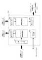
まず、本実施の形態にかかる画像処理装置の原理について説明する。図1は、この発明の本実施の形態にかかる画像処理装置の構成を機能的に示すブロック図である。図1において、画像処理装置は、以下に示す5つのユニットを含む構成である。
【0048】
上記5つのユニットとは、画像データ制御ユニット100と、画像データを読み取る画像読取ユニット101と、画像を蓄積する画像メモリーを制御して画像データの書込み/読出しをおこなう画像メモリー制御ユニット102と、画像データに対し加工編集等の画像処理を施す画像処理ユニット103と、画像データを転写紙等に書き込む画像書込ユニット104と、である。
【0049】
上記各ユニットは、画像データ制御ユニット100を中心に、画像読取ユニット101と、画像メモリー制御ユニット102と、画像処理ユニット103と、画像書込ユニット104とがそれぞれ画像データ制御ユニット100に接続されている。
【0050】
(画像データ制御ユニット100)
画像データ制御ユニット100によりおこなわれる処理としては以下のようなものがある。たとえば、
【0051】
(1)データのバス転送効率を向上させるためのデータ圧縮処理(一次圧縮)、
(2)一次圧縮データの画像データへの転送処理、
(3)画像合成処理(複数ユニットからの画像データを合成することが可能である。また、データバス上での合成も含む。)、
(4)画像シフト処理(主走査および副走査方向の画像のシフト)、
(5)画像領域拡張処理(画像領域を周辺へ任意量だけ拡大することが可能)、
(6)画像変倍処理(たとえば、50%または200%の固定変倍)、
(7)パラレルバス・インターフェース処理、
(8)シリアルバス・インターフェース処理(後述するプロセス・コントローラー211とのインターフェース)、
(9)パラレルデータとシリアルデータのフォーマット変換処理、
(10)画像読取ユニット101とのインターフェース処理、
(11)画像処理ユニット103とのインターフェース処理、
(12)データの伸張処理、
等である。
【0052】
(画像読取ユニット101)
画像読取ユニット101によりおこなわれる処理としては以下のようなものがある。たとえば、
【0053】
(1)光学系による原稿反射光の読み取り処理、
(2)CCD(Charge Coupled Device:電荷結合素子)での電気信号への変換処理、
(3)A/D変換器でのディジタル化処理、
(4)シェーディング補正処理(光源の照度分布ムラを補正する処理)、
(5)スキャナーγ補正処理(読み取り系の濃度特性を補正する処理)、
等である。
【0054】
(画像メモリー制御ユニット102)
画像メモリー制御ユニット102によりおこなわれる処理としては以下のようなものがある。たとえば、
【0055】
(1)システム・コントローラーとのインターフェース制御処理、
(2)パラレルバス制御処理(パラレルバスとのインターフェース制御処理)、
(3)ネットワーク制御処理、
(4)シリアルバス制御処理(複数の外部シリアルポートの制御処理)、
(5)内部バスインターフェース制御処理(操作部とのコマンド制御処理)、
(6)ローカルバス制御処理(システム・コントローラーを起動させるためのROM、RAM、フォントデータのアクセス制御処理)、
(7)メモリー・モジュールの動作制御処理(メモリー・モジュールの書き込み/読み出し制御処理等)、
(8)メモリー・モジュールへのアクセス制御処理(複数のユニットからのメモリー・アクセス要求の調停をおこなう処理)、
(9)データの圧縮/伸張処理(メモリー有効活用のためのデータ量の削減するための処理)、
(10)画像編集処理(メモリー領域のデータクリア、画像データの回転処理、メモリー上での画像合成処理等)、
等である。
【0056】
(画像処理ユニット103)
画像処理ユニット103によりおこなわれる処理としては以下のようなものがある。たとえば、
【0057】
(1)シェーディング補正処理(光源の照度分布ムラを補正する処理)、
(2)スキャナーγ補正処理(読み取り系の濃度特性を補正する処理)、
(3)MTF補正処理、
(4)平滑処理、
(5)主走査方向の任意変倍処理、
(6)濃度変換(γ変換処理:濃度ノッチに対応)、
(7)単純多値化処理、
(8)単純二値化処理、
(9)誤差拡散処理、
(10)ディザ処理、
(11)ドット配置位相制御処理(右寄りドット、左寄りドット)、
(12)孤立点除去処理、
(13)像域分離処理(色判定、属性判定、適応処理)、
(14)密度変換処理、
等である。
【0058】
(画像書込ユニット104)
画像書込ユニット104によりおこなわれる処理としては以下のようなものがある。たとえば、
【0059】
(1)エッジ平滑処理(ジャギー補正処理)、
(2)ドット再配置のための補正処理、
(3)画像信号のパルス制御処理、
(4)パラレルデータとシリアルデータのフォーマット変換処理、
等である。
【0060】
(ディジタル複合機のハードウエア構成)
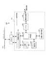
つぎに、本実施の形態にかかる画像処理装置がディジタル複合機を構成する場合のハードウエア構成について説明する。図2は本実施の形態にかかる画像処理装置のハードウエア構成の一例を示すブロック図である。
【0061】
図2のブロック図において、本実施の形態にかかる画像処理装置は、読取ユニット201と、センサー・ボード・ユニット202と、画像データ制御部203と、画像処理プロセッサー204と、ビデオ・データ制御部205と、作像ユニット(エンジン)206とを備える。また、本実施の形態にかかる画像処理装置は、シリアルバス210を介して、プロセス・コントローラー211と、RAM212と、ROM213とを備える。
【0062】
また、本実施の形態にかかる画像処理装置は、パラレルバス220を介して、画像メモリー・アクセス制御部221とファクシミリ制御ユニット224とを備え、さらに、画像メモリー・アクセス制御部221に接続されるメモリー・モジュール222と、システム・コントローラー231と、RAM232と、ROM233と、操作パネル234とを備える。
【0063】
ここで、上記各構成部と、図1に示した各ユニット100〜104との関係について説明する。すなわち、読取ユニット201およびセンサー・ボード・ユニット202により、図1に示した画像読取ユニット101の機能を実現する。また同様に、画像データ制御部203により、画像データ制御ユニット100の機能を実現する。また同様に、画像処理プロセッサー204により画像処理ユニット103の機能を実現する。
【0064】
また同様に、ビデオ・データ制御部205および作像ユニット(エンジン)206により画像書込ユニット104を実現する。また同様に、画像メモリー・アクセス制御部221およびメモリー・モジュール222により画像メモリー制御ユニット102を実現する。
【0065】
つぎに、各構成部の内容について説明する。原稿を光学的に読み取る読取ユニット201は、ランプとミラーとレンズから構成され、原稿に対するランプ照射の反射光をミラーおよびレンズにより受光素子に集光する。
【0066】
受光素子、たとえばCCDは、センサー・ボード・ユニット202に搭載され、CCDにおいて電気信号に変換された画像データはディジタル信号に変換された後、センサー・ボード・ユニット202から出力(送信)される。
【0067】
センサー・ボード・ユニット202から出力(送信)された画像データは画像データ制御部203に入力(受信)される。機能デバイス(処理ユニット)およびデータバス間における画像データの伝送は画像データ制御部203がすべて制御する。
【0068】
画像データ制御部203は、画像データに関し、センサー・ボード・ユニット202、パラレルバス220、画像処理プロセッサー204間のデータ転送、画像データに対するプロセス・コントローラー211と画像処理装置の全体制御を司るシステム・コントローラー231との間の通信をおこなう。また、RAM212はプロセス・コントローラー211のワークエリアとして使用され、ROM213はプロセス・コントローラー211のブートプログラム等を記憶している。
【0069】
センサー・ボード・ユニット202から出力(送信)された画像データは画像データ制御部203を経由して画像処理プロセッサー204に転送(送信)され、光学系およびディジタル信号への量子化にともなう信号劣化(スキャナー系の信号劣化とする)を補正し、再度、画像データ制御部203へ出力(送信)される。
【0070】
画像メモリー・アクセス制御部221は、メモリー・モジュール222に対する画像データの書き込み/読み出しを制御する。また、パラレルバス220に接続される各構成部の動作を制御する。また、RAM232はシステム・コントローラー231のワークエリアとして使用され、ROM233はシステム・コントローラー231のブートプログラム等を記憶している。
【0071】
操作パネル234は、画像処理装置がおこなうべき処理を入力する。たとえば、処理の種類(複写、ファクシミリ送信、画像読込、プリント等)および処理の枚数等を入力する。これにより、画像データ制御情報の入力をおこなうことができる。なお、ファクシミリ制御ユニット224の内容については後述する。
【0072】
つぎに、読み取った画像データにはメモリー・モジュール222に蓄積して再利用するジョブと、メモリー・モジュール222に蓄積しないジョブとがあり、それぞれの場合について説明する。メモリー・モジュール222に蓄積する例としては、1枚の原稿について複数枚を複写する場合に、読取ユニット201を1回だけ動作させ、読取ユニット201により読み取った画像データをメモリー・モジュール222に蓄積し、蓄積された画像データを複数回読み出すという方法がある。
【0073】
メモリー・モジュール222を使わない例としては、1枚の原稿を1枚だけ複写する場合に、読み取り画像データをそのまま再生すればよいので、画像メモリー・アクセス制御部221によるメモリー・モジュール222へのアクセスをおこなう必要はない。
【0074】
まず、メモリー・モジュール222を使わない場合、画像処理プロセッサー204から画像データ制御部203へ転送されたデータは、再度画像データ制御部203から画像処理プロセッサー204へ戻される。画像処理プロセッサー204においては、センサー・ボード・ユニット202におけるCCDによる輝度データを面積階調に変換するための画質処理をおこなう。
【0075】
画質処理後の画像データは画像処理プロセッサー204からビデオ・データ制御部205に転送される。面積階調に変化された信号に対し、ドット配置に関する後処理およびドットを再現するためのパルス制御をおこない、その後、作像ユニット206において転写紙上に再生画像を形成する。
【0076】
つぎに、メモリー・モジュール222に蓄積し画像読み出し時に付加的な処理、たとえば画像方向の回転、画像の合成等をおこなう場合の画像データの流れについて説明する。画像処理プロセッサー204から画像データ制御部203へ転送された画像データは、画像データ制御部203からパラレルバス220を経由して画像メモリー・アクセス制御部221に送られる。
【0077】
ここでは、システム・コントローラー231の制御に基づいて画像データとメモリー・モジュール222のアクセス制御、外部PC(パーソナル・コンピューター)223のプリント用データの展開、メモリー・モジュール222の有効活用のための画像データの圧縮/伸張をおこなう。
【0078】
画像メモリー・アクセス制御部221へ送られた画像データは、データ圧縮後メモリー・モジュール222へ蓄積され、蓄積された画像データは必要に応じて読み出される。読み出された画像データは伸張され、本来の画像データに戻し画像メモリー・アクセス制御部221からパラレルバス220を経由して画像データ制御部203へ戻される。
【0079】
画像データ制御部203から画像処理プロセッサー204への転送後は画質処理、およびビデオ・データ制御部205でのパルス制御をおこない、作像ユニット206において転写紙上に再生画像を形成する。
【0080】
画像データの流れにおいて、パラレルバス220および画像データ制御部203でのバス制御により、ディジタル複合機の機能を実現する。ファクシミリ送信機能は読み取られた画像データを画像処理プロセッサー204にて画像処理を実施し、画像データ制御部203およびパラレルバス220を経由してファクシミリ制御ユニット224へ転送する。ファクシミリ制御ユニット224にて通信網へのデータ変換をおこない、公衆回線(PN)225へファクシミリデータとして送信する。
【0081】
一方、受信されたファクシミリデータは、公衆回線(PN)225からの回線データをファクシミリ制御ユニット224にて画像データへ変換され、パラレルバス220および画像データ制御部203を経由して画像処理プロセッサー204へ転送される。この場合、特別な画質処理はおこなわず、ビデオ・データ制御部205においてドット再配置およびパルス制御をおこない、作像ユニット206において転写紙上に再生画像を形成する。
【0082】
複数ジョブ、たとえば、コピー機能、ファクシミリ送受信機能、プリンター出力機能が並行に動作する状況において、読取ユニット201、作像ユニット206およびパラレルバス220の使用権のジョブへの割り振りをシステム・コントローラー231およびプロセス・コントローラー211において制御する。
【0083】
プロセス・コントローラー211は画像データの流れを制御し、システム・コントローラー231はシステム全体を制御し、各リソースの起動を管理する。また、ディジタル複合機の機能選択は操作パネル(操作部)234において選択入力し、コピー機能、ファクシミリ機能等の処理内容を設定する。
【0084】
システム・コントローラー231とプロセス・コントローラー211は、パラレルバス220、画像データ制御部203およびシリアルバス210を介して相互に通信をおこなう。具体的には、画像データ制御部203内においてパラレルバス220とシリアルバス210とのデータ・インターフェースのためのデータフォーマット変換をおこなうことにより、システム・コントローラー231とプロセス・コントローラー211間の通信をおこなう。
【0085】
(画像処理ユニット103/画像処理プロセッサー204)
つぎに、画像処理ユニット103を構成する画像処理プロセッサー204における処理の概要について説明する。図3は本実施の形態にかかる画像処理装置の画像処理プロセッサー204の処理の概要を示すブロック図である。
【0086】
図3のブロック図において、画像処理プロセッサー204は、第1入力I/F301と、スキャナー画像処理部302と、第1出力I/F303と、第2入力I/F304と、画質処理部305と、第2出力I/F306とを含む構成となっている。
【0087】
上記構成において、読み取られた画像データはセンサー・ボード・ユニット202、画像データ制御部203を介して画像処理プロセッサー204の第1入力インターフェース(I/F)301からスキャナー画像処理部302へ伝達される。
【0088】
スキャナー画像処理部302は読み取られた画像データの劣化を補正することを目的とし、具体的には、シェーディング補正、スキャナーγ補正、MTF補正等をおこなう。補正処理ではないが、拡大/縮小の変倍処理もおこなうことができる。読み取り画像データの補正処理が終了すると、第1出力インターフェース(I/F)303を介して画像データ制御部203へ画像データを転送する。
【0089】
転写紙への出力の際は、画像データ制御部203からの画像データを第2入力I/F304より受信し、画質処理部305において面積階調処理をおこなう。画質処理後の画像データは第2出力I/F306を介してビデオ・データ制御部205または画像データ制御部203へ出力される。
【0090】
画質処理部305における面積階調処理は、濃度変換処理、ディザ処理、誤差拡散処理等があり、階調情報の面積近似を主な処理とする。一旦、スキャナー画像処理部302により処理された画像データをメモリー・モジュール222に蓄積しておけば、画質処理部305により画質処理を変えることによって種々の再生画像を確認することができる。
【0091】
たとえば、再生画像の濃度を振って(変更して)みたり、ディザマトリクスの線数を変更してみたりすることにより、再生画像の雰囲気を容易に変更することができる。この際、処理を変更するごとに画像を読取ユニット201からの読み込みをやり直す必要はなく、メモリー・モジュール222から蓄積された画像データを読み出すことにより、同一画像データに対して、何度でも異なる処理を迅速に実施することができる。
【0092】
また、単体スキャナーの場合、スキャナー画像処理と階調処理を合わせて実施し、画像データ制御部203へ出力する。処理内容はプログラマブルに変更することができる。処理の切り替え、処理手順の変更等はシリアルI/F308を介してコマンド制御部307において管理する。
【0093】
(画像データ制御ユニット100/画像データ制御部203)
つぎに、画像データ制御ユニット100を構成する画像データ制御部203における処理の概要について説明する。図4は本実施の形態にかかる画像処理装置の画像データ制御部203の処理の概要を示すブロック図である。
【0094】
図4のブロック図において、画像データ入出力制御部401は、センサー・ボード・ユニット202からの画像データを入力(受信)し、画像処理プロセッサー204に対して画像データを出力(送信)する。すなわち、画像データ入出力制御部401は、画像読取ユニット101と画像処理ユニット103(画像処理プロセッサー204)とを接続するための構成部であり、画像読取ユニット101により読み取られた画像データを画像処理ユニット103へ送信するためだけの専用の入出力部であるといえる。
【0095】
また、画像データ入力制御部402は、画像処理プロセッサー204でスキャナー画像補正された画像データを入力(受信)する。入力された画像データはパラレルバス220における転送効率を高めるために、データ圧縮部403においてデータ圧縮処理をおこなう。その後、データ変換部404を経由し、パラレルデータI/F405を介してパラレルバス220へ送出される。なお、データ圧縮部403の構成および動作については後に詳述する。
【0096】
パラレルバス220からパラレルデータI/F405を介して入力される画像データは、バス転送のために圧縮されているため、データ変換部404を経由してデータ伸張部406へ送られ、そこでデータ伸張処理をおこなう。伸張された画像データは画像データ出力制御部407において画像処理プロセッサー204へ転送される。なお、データ伸張部406の構成および動作については後に詳述する。
【0097】
また、画像データ制御部203は、パラレルデータとシリアルデータの変換機能も備えている。システム・コントローラー231はパラレルバス220にデータを転送し、プロセス・コントローラー211はシリアルバス210にデータを転送する。画像データ制御部203は2つのコントローラーの通信のためにデータ変換をおこなう。
【0098】
また、シリアルデータI/Fは、シリアルバス210を介してプロセス・コントローラーとのデータのやりとりをする第1シリアルデータI/F408と、画像処理プロセッサー204とのデータのやりとりに用いる第2シリアルデータI/F409を備える。画像処理プロセッサー204との間に独立に1系統持つことにより、画像処理プロセッサー204とのインターフェースを円滑化することができる。
【0099】
コマンド制御部410は、入力された命令にしたがって、上述した画像データ制御部203内の各構成部および各インターフェースの動作を制御する。特に、データ圧縮部403とデータ伸張部406とからなるデータ圧縮伸張部411の動作制御をおこなう。この制御内容については後に詳述する。
【0100】
(画像書込ユニット104/ビデオ・データ制御部205)
つぎに、画像書込ユニット104の一部を構成するビデオ・データ制御部205における処理の概要について説明する。図5は本実施の形態にかかる画像処理装置のビデオ・データ制御部205の処理の概要を示すブロック図である。
【0101】
図5のブロック図において、ビデオ・データ制御部205は、入力される画像データに対して、作像ユニット206の特性に応じて、追加の処理をおこなう。すなわち、エッジ平滑処理部501がエッジ平滑処理によるドットの再配置処理をおこない、パルス制御部502がドット形成のための画像信号のパルス制御をおこない、上記の処理がおこなわれた画像データを作像ユニット206へ出力する。
【0102】
画像データの変換とは別に、パラレルデータとシリアルデータのフォーマット変換機能を備え、ビデオ・データ制御部205単体でもシステム・コントローラー231とプロセス・コントローラー211の通信に対応することができる。すなわち、パラレルデータを送受信するパラレルデータI/F503と、シリアルデータを送受信するシリアルデータI/F504と、パラレルデータI/F503およびシリアルデータI/F504により受信されたデータを相互に変換するデータ変換部505とを備えることにより、両データのフォーマットを変換する。
【0103】
(画像メモリー制御ユニット102/画像メモリー・アクセス制御部221)
つぎに、画像メモリー制御ユニット102の一部を構成する画像メモリー・アクセス制御部221における処理の概要について説明する。図6は本実施の形態にかかる画像処理装置の画像メモリー・アクセス制御部221の処理の概要を示すブロック図である。
【0104】
図6のブロック図において、画像メモリー・アクセス制御部221は、パラレルバス220との画像データのインターフェースを管理し、また、メモリー・モジュール222への画像データのアクセス、すなわち格納(書込み)/読出しを制御し、また、主に外部のPC223から入力されるコードデータの画像データへの展開を制御する。
【0105】
そのために、画像メモリー・アクセス制御部221は、パラレルデータI/F601と、システム・コントローラーI/F602と、メモリー・アクセス制御部603と、ラインバッファー604と、ビデオ制御部605と、データ圧縮部606と、データ伸張部607と、データ変換部608と、を含む構成である。
【0106】
ここで、パラレルデータI/F601は、パラレルバス220との画像データのインターフェースを管理する。また、メモリー・アクセス制御部603は、メモリー・モジュール222への画像データのアクセス、すなわち格納(書込み)/読出しを制御する。
【0107】
また、入力されたコードデータは、ラインバッファー604において、ローカル領域でのデータの格納をおこなう。ラインバッファー604に格納されたコードデータは、システム・コントローラーI/F602を介して入力されたシステム・コントローラー231からの展開処理命令に基づき、ビデオ制御部605において画像データに展開される。
【0108】
展開された画像データもしくはパラレルデータI/F601を介してパラレルバス220から入力された画像データは、メモリー・モジュール222に格納される。この場合、データ変換部608において格納対象となる画像データを選択し、データ圧縮部606においてメモリー使用効率を上げるためにデータ圧縮をおこない、メモリー・アクセス制御部603にてメモリー・モジュール222のアドレスを管理しながらメモリー・モジュール222に画像データを格納(書込)する。
【0109】
メモリー・モジュール222に格納(蓄積)された画像データの読み出しは、メモリー・アクセス制御部603において読み出し先アドレスを制御し、読み出された画像データをデータ伸張部607において伸張する。伸張された画像データをパラレルバス220へ転送する場合、パラレルデータI/F601を介してデータ転送をおこなう。
【0110】
(ファクシミリ制御ユニット224の構成)
つぎに、ファクシミリ制御ユニット224の機能的な構成について説明する。図7は、本実施の形態における画像処理装置のファクシミリ制御ユニット224の構成を示すブロック図である。
【0111】
図7のブロック図において、ファクシミリ制御ユニット224は、ファクシミリ送受信部701と外部I/F702とから構成される。ここで、ファクシミリ送受信部701は、画像データを通信形式に変換して外部回線に送信し、また、外部からのデータを画像データに戻して外部I/F702およびパラレルバス220を介して作像ユニットにおいて記録出力する。
【0112】
ファクシミリ送受信部701は、ファクシミリ画像処理部703、画像メモリー704、メモリー制御部705、データ制御部706、画像圧縮伸張部707、モデム708および網制御装置709を含む構成である。
【0113】
このうち、ファクシミリ画像処理に関し、受信画像に対する二値スムージング処理は、図5に示したビデオ・データ制御部205内のエッジ平滑処理部501においておこなう。また、画像メモリー704に関しても、出力バッファー機能に関しては画像メモリー・アクセス制御部221およびメモリー・モジュール222にその機能の一部を移行する。
【0114】
このように構成されたファクシミリ送受信部701では、画像データの伝送を開始するとき、データ制御部706がメモリー制御部705に指令し、画像メモリー704から蓄積している画像データを順次読み出させる。読み出された画像データは、ファクシミリ画像処理部703によって元の信号に復元されるとともに、密度変換処理および変倍処理がなされ、データ制御部706に加えられる。
【0115】
データ制御部706に加えられた画像データは、画像圧縮伸張部707によって符号圧縮され、モデム708によって変調された後、網制御装置709を介して宛先へと送出される。そして、送信が完了した画像情報は、画像メモリー704から削除される。
【0116】
受信時には、受信画像は一旦画像メモリー704に蓄積され、そのときに受信画像を記録出力可能であれば、1枚分の画像の受信を完了した時点で記録出力する。また、複写動作時に発呼されて受信を開始したときは、画像メモリー704の使用率が所定値、たとえば80%に達するまでは画像メモリー704に蓄積し、画像メモリー704の使用率が80%に達した場合には、そのときに実行している書き込み動作を強制的に中断し、受信画像を画像メモリー704から読み出し記録出力する。
【0117】
このとき画像メモリー704から読み出した受信画像は画像メモリー704から削除し、画像メモリー704の使用率が所定値、たとえば10%まで低下した時点で中断していた書き込み動作を再開し、その書き込み動作をすべて終了した時点で、残りの受信画像を記録出力する。また、書き込み動作を中断した後に、再開できるように中断時における書き込み動作のための各種パラメーターを内部的に退避し、再開時に、パラメーターを内部的に復帰する。
【0118】
(ユニット構成)
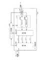
つぎに、本実施の形態にかかる画像処理装置のユニット構成について説明する。図8は、画像処理装置がディジタル複合機の場合のユニット構成の一例を示すブロック図である。
【0119】
図8に示すようにディジタル複合機の場合においては、画像読取ユニット101、画像エンジン制御ユニット800、画像書込ユニット104の3つのユニットで構成され、各ユニットはそれぞれ単独のPCB基板で管理できる。
【0120】
画像読取ユニット101は、CCD801、A/D変換モジュール802、ゲイン制御モジュール803等から構成され、光学的に読み取られた光学画像情報をディジタル画像信号に変換する。
【0121】
画像エンジン制御ユニット800は、システム・コントローラー231、プロセス・コントローラー211、画像メモリー制御ユニット102内のメモリー・モジュール222を中心に構成し、画像処理プロセッサー204、画像メモリー・アクセス制御部221およびバス制御をおこなう画像データ制御部203をひとまとまりとしてあつかう。
【0122】
また、画像書込ユニット104は、ビデオ・データ制御部205を中心に作像ユニット206を含む構成である。
【0123】
これらのユニット構成において、画像読取ユニット101の仕様、性能が変更になった場合、ディジタル複合機のシステムでは画像読取ユニット101のみを変更すれば、データ・インターフェースは保持されているのでほかのユニットは変更する必要がない。また、作像ユニット(エンジン)206が変更になった場合、画像書込ユニット104のみ変更すればシステムの再構築が可能となる。
【0124】
このように、入出力デバイスに依存するユニットは別々な構成でシステムを構築するので、データ・インターフェースが保持されている限り、最小ユニットの交換のみでシステムのアップグレードがおこなえる。
【0125】
図8に示した画像エンジン制御ユニット800の構成において、画像処理プロセッサー204、画像データ制御部203、画像メモリー・アクセス制御部221の各モジュール(構成部)は独立なモジュールで構成する。したがって、画像エンジン制御ユニット800からコントローラーへの転用は不要なモジュールを削除することで、共通モジュールは汎用的に使用されている。このように、画像エンジン制御用のモジュール、コントローラー用のモジュールを別々に作成せずに、同様な機能は共通のモジュールを使用することで実現している。
【0126】
(圧縮処理の内容)
つぎに、本実施の形態にかかる画像処理装置の画像データの圧縮処理について説明する。なお、ここでは、画像データ制御部203内のデータ圧縮部403(図4参照)の構成および動作について説明するが、画像メモリー・アクセス制御部221内のデータ圧縮部606(図6参照)、もしくは、ファクシミリ送受信部701内の画像圧縮伸張部707も、同様の構成とすることができる。
【0127】
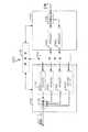
はじめに、データ圧縮部403の構成および動作について説明する。図9は、本実施の形態における画像処理装置のデータ圧縮部403の構成を示すブロック図であり、図10は、データ圧縮部403の処理タイミングを示す説明図である。
【0128】
図9において、データ圧縮部403は、画像データを格納する1ポートFIFOメモリーFM1、FM2およびFM3からなるラインメモリー群901と、画像データを圧縮する圧縮器902と、画像データをそのまま圧縮器902に送出する回路TL4と、入力する画像データの出力先を切り替える切替器903と、ラインメモリー群901、圧縮器902、切替器903を制御するコマンド制御部410とから構成される。なお、以降において画像データをそのまま送出する回路をスルーラインと称することとする。
【0129】
なお、ここでは説明の簡単のために、圧縮器902で圧縮する圧縮領域としては、図18に示したように主走査(画素)方向に4画素、副走査(ライン)方向に4ラインからなる1ライン4画素×4ラインの矩形領域とする。使用の態様によっては、たとえば、動画圧縮標準のMPEG(Motion Picture
Expert Group)方式で採用されているDCT(Discrete
Cosine Transformation:離散コサイン変換)における1ライン8画素×8ラインの領域であってもよい。すなわち、この圧縮領域の大きさは使用するハードウエアやアプリケーションに依存したものであり、特に1ライン4画素×4ラインに限定するものではない。
【0130】
画像データの圧縮については、まず、画像処理プロセッサー204から出力された画像データを入力する。画像データは連続的に切替器903に入力するので、切替器903は、はじめの4画素分(P11、P12、P13、P14)の画像データ(第1ラインの画像データ)については、FIFOメモリーFM1に送出し、つぎの1画素(第5画素:P21)の画像データが入力する際に、出力先をFIFOメモリーFM2に切り替え、当該画素を含む4画素分の画像データ(第2ラインの画像データ)をFIFOメモリーFM2に送出する。
【0131】
同様に、切替器903は、第9画素(P31)の画像データが入力する際に、出力先をFIFOメモリーFM3に切り替え、当該画素を含む4画素分の画像データ(第3ラインの画像データ)をFIFOメモリーFM3に送出する。
【0132】
つぎの第13画素(P41)の画像データが入力する際に、切替器903は、出力先をスルーラインTL4に切り替え、当該画素を含む4画素分の画像データ(第4ラインの画像データ)を圧縮器902に直接送出し、同時に、コマンド制御部410の制御の下、FIFOメモリーFM1、FM2およびFM3にそれぞれ格納された第1ラインから第3ラインの画像データを読み出し、圧縮器902に送出する(図10参照)。
【0133】
圧縮器902は、第1ラインから第4ラインの画像データを入力し、一括して圧縮する。以上の動作により、1ライン4画素×4ライン分の画像データが一括して圧縮される。圧縮されたデータは、コマンド制御部410の制御の下、画像処理プロセッサー204に出力される。
【0134】
一方、第17画素目の画像データが入力する際に、切替器903は、画像データの出力先をFIFOメモリーFM1に切り替え、第5ラインの画像データをFIFOメモリーFM1に送出する。第6ラインおよび第7ラインの画像データについては順次FIFOメモリーFM2およびFM3に送出する。第8ラインの画像データについては、圧縮器902に直接送出し、同時に、FIFOメモリーFM1、FM2およびFM3に格納された第5、6および7ラインを圧縮器に送出する。
【0135】
以降、同様の制御を繰り返すことにより、画像処理プロセッサー204から連続的に入力する画像データを円滑に圧縮することが可能となる。データ圧縮部403は、従来技術にかかるデータ圧縮部1601(図16参照)より1ポートFIFOメモリーを2本削減することが可能となり、データ圧縮部1901(図19参照)より2ポートFIFOメモリーを1本削減することが可能となる。
【0136】
なお、使用の態様によっては、ラインメモリー群901を、ラインメモリーとすることなく(n−1)ライン分の画像データを格納するメモリーに置き換えることによっても、従来技術にかかるデータ圧縮部1601より1ライン分のメモリーを削減することが可能となる。しかしながら、ラインメモリー群901を使用することにより、個別に設計された単一のメモリーとするよりも、簡便な制御方法を用いることができ、また、回路設計が容易となり、装置規模を小さくすることが可能となる。
【0137】
(伸張処理の内容)
つぎに、本実施の形態にかかる画像処理装置の画像データの伸張処理について説明する。なお、ここでは、画像データ制御部203内のデータ伸張部406(図4参照)の構成および動作について説明するが、画像メモリー・アクセス制御部221内のデータ伸張部607(図6参照)、もしくは、ファクシミリ送受信部701内の画像圧縮伸張部707(図7参照)も、同様の構成とすることができる。
【0138】
はじめに、データ伸張部406の構成および動作について説明する。図11は、本実施の形態における画像処理装置のデータ伸張部406の構成を示すブロック図であり、図12は、データ伸張部406の処理タイミングを示す説明図である。
【0139】
図11において、データ伸張部406は、1ライン4画素×4ラインごとに圧縮された画像データを格納する1ポートFIFOメモリーFMI1とFMI2からなる入力側メモリー群1101と、圧縮された画像データを伸張する伸張器1102と、伸張された画像データを格納する1ポートFIFOメモリーFM2、FM3およびFM4からなる出力側メモリー群1103と、圧縮された画像データをFMI1およびFMI2のいずれに出力するかを切り替える切替器1104と、伸張された画像データの入力先を切り替える切替器1105と、伸張器1102から出力された画像データを切替器1105に直接送出する回路であるスルーラインTL1と、から構成される。
【0140】
なお、コマンド制御部410は、入力側メモリー群1101、伸張器1102、出力側メモリー群1103および切替器1105、1106を制御する。
【0141】
図12に示したように画像データの伸張については、まず、パラレルバス220(図4参照)を介して画像データを順次入力する。この画像データは、たとえば、メモリー・モジュール222(図2参照)に格納され、圧縮された画像データであり、1ラインを4画素とする4ラインの画像データが一括して圧縮されたものである。
【0142】
入力した画像データは、切替器1104によりFIFOメモリーFMI1に、つぎの画像データはFIFOメモリーFMI2に、というように切り替えられ格納される。伸張器1102は、圧縮された第1ラインから第4ラインまでのひとかたまりの圧縮データをFIFOメモリーFMI1から入力し、伸張する。
【0143】
伸張されたデータは、コマンド制御部410の制御の下、第1ラインに対しては、スルーラインTL1を介して切替器1105に直接送出するとともに、第2ラインから第4ラインの画像データをそれぞれFIFOメモリーFM2、FM3およびFM4へ送出する。
【0144】
切替器1105から、伸張器1102により伸張された第1ラインの画像データを送出し終えた際に、コマンド制御部410は、切替器1105の画像データの入力先をFIFOメモリーFM2に切り替え、同時にFIFOメモリーFM2から第2ラインの画像データを読み出す制御をおこなう。この制御により、画像データがとぎれることなくデータ伸張部406から出力させることが可能となる。同様にして、第3ラインおよび第4ラインの画像データをデータ伸張部406の外部に送出する。
【0145】
第4ラインの画像データをFIFOメモリーFM4から読み出し終えた後、コマンド制御部410は、FIFOメモリーFMI2にあらかじめ格納されていた第5ラインから第8ラインの画像データを伸張器1102に送出する。伸張器1102では、この第5ラインから第8ラインの画像データを一括して伸張する。伸張器1102は、第5ラインの画像データに関しては、切替器1105に直接送出するとともに、第9ラインから第12ラインまではFIFOメモリーFM2からFM4にそれぞれ格納する。この格納されたデータは、コマンド制御部410の制御の下、順次読み出され、データ伸張部406の外部に送出される。
【0146】
本実施の形態にかかるデータ伸張部406は、上述の制御をおこなうことにより、データ伸張部2101(図21参照)に比して1本分の1ポートFIFOメモリーを削減でき、また、2ポートFIFOメモリーを1ポートFIFOメモリーに置換することが可能であり、回路規模を縮小することが可能となる。
【0147】
なお、使用の態様によっては、出力側メモリー群1103を、ラインメモリーとすることなく(n−1)ライン分の画像データを格納するメモリーに置き換えることによっても、従来技術にかかるデータ圧縮部2101より1ライン分のメモリーを削減することが可能となる。しかしながら、出力側メモリー群1103を使用することにより、個別に設計された単一のメモリーとするよりも、簡便な制御方法を用いることができ、また、回路設計が容易となり、装置規模を小さくすることが可能となる。
【0148】
〔実施の形態2〕
実施の形態2では、データ伸張部における回路規模のさらに小さな画像処理装置について説明する。なお、本実施の形態では、実施の形態1と同様の部分については同一の符合を配することとし、その説明を省略する。
【0149】
はじめに、本実施の形態にかかるデータ伸張部の構成および動作について説明する。図13は、本実施の形態における画像処理装置のデータ伸張部の構成を示すブロック図であり、図14は、このデータ伸張部の処理タイミングを示す説明図である。
【0150】
図13において、データ伸張部1301は、1ライン4画素×4ラインごとに圧縮された画像データを格納する1ポートFIFOメモリーFMI1とFMI2とからなる入力側メモリー群1101と、圧縮された画像データを伸張する伸張器1102と、伸張された4ライン分の画像データのうち抽出すべき1ライン分の画像データを抽出する抽出器1302と、圧縮された画像データをFMI1およびFMI2のいずれに出力するかを切り替える切替器1104と、から構成される。なお、コマンド制御部410は、入力側メモリー群1101、伸張器1102、抽出器1302および切替器1104とを制御する。
【0151】
図14に示したように、画像データの伸張については、まず、パラレルバス220(図4参照)を介して画像データを入力する。入力した画像データは、切替器1104によりFIFOメモリーFMI1に、つぎの画像データはFIFOメモリーFMI2に、というように切り替えられて格納される。伸張器1102は、まず、圧縮された第1ラインから第4ラインまでのひとかたまりの圧縮データをFIFOメモリーFMI1から入力し、伸張する。
【0152】
伸張された第1ラインから第4ラインの画像データは、抽出器1302において、第1ラインが抽出される。抽出器1302における画像データの抽出の態様は様々に考えられるが、たとえば切替器1104のような適当なスイッチ切替により、データ伸張部1301外部と結線する方法が挙げられる。すなわち、コマンド制御部410の制御により、1ライン分の画像データが伸張器1102から出力される。
【0153】
コマンド制御部410は、第1ラインの画像データの抽出(出力)を検知し、再びFIFOメモリーMFI1に格納された第1ラインから第4ラインまでの圧縮された画像データを読み出す。伸張器1102では、この読み出された4ライン分の画像データを一括して伸張する。抽出器1302では、伸張された第1ラインから第4ラインまでの画像データのうち、今度は、第2ラインを抽出する。以降同様にして、伸張器1102では、一括して全4ラインを伸張し、抽出器1302で、第3ラインを抽出し、つぎのサイクルでは第4ラインを抽出する。
【0154】
続いて、コマンド制御部410の制御の下、FIFOメモリーFMI2に格納された第5ラインから第8ラインまでの圧縮された画像データを読み出し、伸張器1102で一括して伸張する。抽出器1302では、伸張された第5ラインから第8ラインまでの画像データのうち、第5ラインを抽出し、以降同様にして、伸張器1102において一括して全4ラインを伸張し、抽出器1302で順次、第6ライン、第7ライン、第8ラインを抽出する。
【0155】
実施の形態2の画像処理装置のデータ伸張部1301では、切替器1104から伸張器1102まで、同一の画像データ(圧縮された4ライン分の画像データ)を4回伸張し、順次必要なラインだけを抽出器1302で抽出し、データ伸張部1301の外部に出力する。このような構成にすることにより、従来技術のデータ伸張部2101(図21参照)に比して、メモリー群2107を削減することが可能となる。したがって、回路規模を著しく縮小することが可能となる。
【0156】
【発明の効果】
以上説明したように、この発明によれば、区分け手段が1ラインをm画素とするnラインからなるm×n画素に画像データを区分けし、格納手段が前記区分け手段により区分けされた画素の画像データを格納し、圧縮手段がm×n画素の画像データを一括して圧縮し、制御手段が、前記区分け手段により区分けされたm×n画素の画像データのうち(n−1)ライン分の画像データを前記格納手段に送出し、残りの1ライン分の画像データについては前記圧縮手段に直接送出するとともに、前記格納手段に格納されたm×(n−1)画素の画像データを前記圧縮手段に送出する制御をおこなうので、格納手段により格納される画像データの容量を1ライン分削減することができ、これにより、回路規模の縮小化を図ることが可能な画像処理装置が得られるという効果を奏する。
【0157】
また、この発明によれば、請求項1に記載の発明において、前記格納手段が、(n−1)本のFIFOメモリーにより構成され、前記制御手段が、前記区分け手段により区分けされた画像データを各ラインごとに前記FIFOメモリーに送出する制御をおこなうので、回路設計を容易におこなうことができ、これにより、回路規模の縮小化を図ることが可能な画像処理装置が得られるという効果を奏する。
【0158】
また、この発明によれば、伸張手段が圧縮されたm×n画素の画像データである圧縮データを一括して伸張し、格納手段が前記伸張手段により伸張された画像データを格納し、制御手段が、前記伸張手段により伸張されたm画素を1ラインとする1ライン分の画像データを前記所定の出力先に直接送出するとともに、残りの(n−1)ライン分の画素の画像データを前記格納手段に送出し、その後当該格納手段に格納された(n−1)ライン分の画素の画像データを前記所定の出力先に送出する制御をおこなうので、格納手段により格納される画像データの容量を1ライン分削減することができ、これにより、回路規模の縮小化を図ることが可能な画像処理装置が得られるという効果を奏する。
【0159】
また、この発明によれば、前記格納手段が、(n−1)本のFIFOメモリーにより構成され、前記制御手段が、前記伸張手段により伸張された画像データを各ラインごとに前記FIFOメモリーに送出する制御をおこなうので、回路設計を容易におこなうことができ、これにより、回路規模の縮小化を図ることが可能な画像処理装置が得られるという効果を奏する。
【0160】
また、この発明によれば、入力手段がm×n画素の画像データごとに圧縮された画像データである圧縮データを入力し、伸張手段が前記入力手段により入力された圧縮データをm×n画素の画像データに一括して伸張し、抽出手段が前記伸張手段により伸張されたm×n画素の画像データからm画素を1ラインとする1ライン分の画像データを抽出し、出力手段が前記抽出手段により抽出された1ライン分の画像データを出力し、検知手段が前記出力手段により前記1ライン分の画像データが出力されたか否かを検知し、制御手段が、前記入力手段を制御して、前記検出手段により画像データの出力が検知された場合に、当該画像データを含む前記圧縮データを再び入力し、さらに、前記抽出手段を制御して、前記抽出手段により従前には抽出されなかった1ライン分の画像データを抽出し、この制御を繰り返すことにより1ラインからnラインまでの画像データを順次出力するので、伸張手段により伸張された画像データを格納する格納手段が不要となり、これにより、回路規模の縮小化を図ることが可能な画像処理装置が得られるという効果を奏する。
【図面の簡単な説明】
【図1】 この発明の実施の形態1にかかる画像処理装置の構成を機能的に示すブロック図である。
【図2】 実施の形態1にかかる画像処理装置のハードウエア構成の一例を示すブロック図である。
【図3】 実施の形態1にかかる画像処理装置の画像処理プロセッサーの処理の概要を示すブロック図である。
【図4】 実施の形態1にかかる画像処理装置の画像データ制御部の処理の概要を示すブロック図である。
【図5】 実施の形態にかかる画像処理装置のビデオ・データ制御部の処理の概要を示すブロック図である。
【図6】 実施の形態1にかかる画像処理装置の画像メモリー・アクセス制御部の処理の概要を示すブロック図である。
【図7】 実施の形態1における画像処理装置のファクシミリ制御ユニットの構成を示すブロック図である。
【図8】 画像処理装置がディジタル複合機の場合のユニット構成の一例を示すブロック図である。
【図9】 実施の形態1における画像処理装置のデータ圧縮部の構成を示すブロック図である。
【図10】 実施の形態1における画像処理装置のデータ圧縮部の処理タイミングを示す説明図である。
【図11】 実施の形態1における画像処理装置のデータ伸張部の構成を示すブロック図である。
【図12】 実施の形態1における画像処理装置のデータ伸張部の処理タイミングを示す説明図である。
【図13】 実施の形態2における画像処理装置のデータ伸張部の構成を示すブロック図である。
【図14】 実施の形態2における画像処理装置のデータ伸張部の処理タイミングを示す説明図である。
【図15】 従来技術にかかるディジタル複合機のハードウエア構成の一例を示すブロック図である。
【図16】 従来のデータ圧縮部の構成の一例を示すブロック図である。
【図17】 図16に示したデータ圧縮部の処理タイミング示す説明図である。
【図18】 データ圧縮部で圧縮される画像データの一例を示す図である。
【図19】 2ポートFIFOメモリーを一部に用いたデータ圧縮部の構成の一例を示した図である。
【図20】 図19に示したデータ圧縮部の処理タイミング示す説明図である。
【図21】 従来のデータ伸張部の構成の一例を示すブロック図である。
【図22】 図21に示したデータ伸張部の処理タイミングを示す説明図である。
【符号の説明】
100 画像データ制御ユニット
101 画像読取ユニット
102 画像メモリー制御ユニット
103 画像処理ユニット
104 画像書込ユニット
201 読取ユニット
202 センサー・ボード・ユニット
203 画像データ制御部
204 画像処理プロセッサー
205 ビデオ・データ制御部
206 作像ユニット
210 シリアルバス
211 プロセス・コントローラー
220 パラレルバス
221 画像メモリー・アクセス制御部
222 メモリー・モジュール
224 ファクシミリ制御ユニット
231 システム・コントローラー
302 スキャナー画像処理部
305 画質処理部
307 コマンド制御部
401 画像データ入出力制御部
402 画像データ入力制御部
403 データ圧縮部
404 データ変換部
406 データ伸張部
407 画像データ出力制御部
410 コマンド制御部
411 データ圧縮伸張部
501 エッジ平滑処理部
502 パルス制御部
505 データ変換部
603 メモリー・アクセス制御部
606 データ圧縮部
607 データ伸張部
608 データ変換部
701 ファクシミリ送受信部
703 ファクシミリ画像処理部
704 画像メモリー
707 画像圧縮伸張部
708 モデム
800 画像エンジン制御ユニット
803 ゲイン制御モジュール
901 ラインメモリー群
902 圧縮器
903 切替器
1101 入力側メモリー群
1102 伸張器
1103 出力側メモリー群
1104,1105 切替器
1301 データ伸張部
1302 抽出器
1102 伸張器
FM1,FM2,FM3,FM4,FMI1,FMI2 FIFOメモリー
TL1,TL2,TL3,TL4 スルーライン[0001]
BACKGROUND OF THE INVENTION
The present invention relates to an image processing apparatus, and more particularly to an image processing apparatus that performs a process of compressing or expanding image data using a line memory.
[0002]
[Prior art]
Conventionally, digital copiers that process image data digitized from analog copiers have appeared. Furthermore, digital copiers not only function as copiers, but also function of facsimile, There are digital multifunction peripherals that combine functions such as printer functions and scanner functions.
[0003]
FIG. 15 is a block diagram illustrating an example of a hardware configuration of a digital multifunction peripheral according to the related art. As shown in FIG. 15, the digital multi-function peripheral 1500 includes a
[0004]
In other words, a
[0005]
Although not shown, the above units are not added to the copying machine, but the copying function part, facsimile function part, printer function part, etc. are combined into units, and the image data input from these units is efficiently used. Digital multi-function machines that process well have been devised.
[0006]
Even if a digital multifunction device adds on a functional unit via a motherboard, or even if each functional unit is created and combined without specializing in a copier, the digital multifunction device is becoming more multifunctional. Image data transfer control is a very important factor from the viewpoint of improving system performance.
[0007]
Therefore, conventionally, image data is compressed as necessary in consideration of transfer control, that is, transfer efficiency of image data between functional units and storage efficiency in a storage unit such as a memory. In other words, the digital multifunction peripheral has improved its performance by compressing the image data.
[0008]
Here, a conventional data compression unit for compressing image data will be described. FIG. 16 is a block diagram illustrating an example of a configuration of a conventional data compression unit, and FIG. 17 is an explanatory diagram illustrating processing timing thereof.
[0009]
In FIG. 16, the
[0010]
Here, for the sake of simplicity of explanation, the compression area compressed by the
[0011]
As shown in FIG. 17, for the compression of the image data, first, the image data of the first line in the rectangular area is written (written) to the FIFO memory FM1a. Next, the image data of the second line is sequentially written in the FIFO memory FM2, the image data of the third line is written in the FIFO memory FM3, and the image data of the fourth line is sequentially written in the FIFO memory FM4. The image data segmentation operation at this time is performed by the
[0012]
At the stage when the image data is written in the FIFO memory FM4, four lines to be compressed by the
[0013]
On the other hand, after the image data of the fourth line is written in the FIFO memory FM4, the image data of the first line of the next rectangular area (the image data of the fifth line) is input. The
[0014]
Thereafter, the image data of the sixth line is sequentially written in the FIFO memory FM2, the data of the seventh line is written in the FIFO memory FM3, and the image data of the eighth line is sequentially written in the FIFO memory FM4.
[0015]
The
[0016]
In the above example, each FIFO memory is a 1-port FIFO memory, but a 2-port FIFO memory can also be used. FIG. 19 is a diagram illustrating an example of a configuration of a data compression unit partially using a 2-port FIFO memory, and FIG. 20 is an explanatory diagram illustrating processing timing thereof. The
[0017]
As shown in FIG. 20, the operation of the
[0018]
Similarly, after the image data of the eighth line is stored in the FIFO memory FM4, the image data of the ninth line is written in the FIFO memory FMD1, while the fifth line to the eighth line stored in the FIFO memories FMD1, FM2, FM3, and FM4. The image data up to the line is read and sent to the
[0019]
In this way, by partially using a 2-port FIFO memory as the FIFO memory, it is possible to reduce the 1-port FIFO memory for one line and to compress a series of image data sequentially input without delay. It becomes possible.
[0020]
On the other hand, the compressed image data is expanded as necessary, and the subsequent processing is performed. In particular, in a digital multi-function peripheral, it is often necessary to decompress compressed image data stored in the
[0021]
Here, a conventional data decompression unit for decompressing image data will be described. FIG. 21 is a block diagram showing an example of the configuration of a conventional data decompression unit, and FIG. 22 is an explanatory diagram showing the processing timing.
[0022]
In FIG. 21, a
[0023]
The input-
[0024]
The output
[0025]
As shown in FIG. 22, for the decompression of the image data, first, the compressed rectangular area image data is sent to the FIFO memory FMI1. The compressed image data is sent to the
[0026]
Next, in accordance with a line data output synchronization signal (not shown), the image data of the first to fourth lines stored in the FIFO memories FM1, FM2, FM3 and FMD4 are sequentially read and sent to a predetermined output destination. . On the other hand, the compressed image data of the fifth to eighth lines stored in the FIFO memory FMI2 is expanded by the
[0027]
As described above, a part of the 2-port FIFO memory is used as the FIFO memory, so that the 1-port FIFO memory for one line can be reduced as in the case of the
[0028]
As described above, conventional image processing apparatuses (digital multi-function peripherals) are required to improve the efficiency of image data transfer control from the viewpoint of improving system performance. A data compression unit and a data decompression unit were provided.
[0029]
Also disclosed is an “image processing apparatus” (for example, Japanese Patent Laid-Open No. 8-274986) that optimizes image processing of read signals, image storage in a memory, parallel operation of a plurality of functions, and respective image processing. Some image processing can be executed with a single image processing configuration.
[0030]
[Problems to be solved by the invention]
However, the above-described conventional digital multi-function peripheral has the following problems. As described above, the data compression unit or the data expansion unit includes a plurality of line memories before and after the compressor or the expansion device. Regarding the line memory, the capacity of image data to be input differs depending on the type and performance of the functional unit to be added on or the functional unit to be combined. Need to design more.
[0031]
In particular, for digital multi-function peripherals that combine each functional unit, some functional units may be replaced due to functional improvements. To cope with such cases, the capacity of one line memory is increased, In addition, it is necessary to design a large number of them.
[0032]
For example, when an original is read with 600 bits per pixel (dot per inch) as 8 bits per pixel, the length is about 8k (1k = 1024) in the longitudinal direction of the A4 size, so 8 bits × in order to store one line of image data. An 8k word line memory is required.
[0033]
That is, the image processing apparatus (digital multi-function peripheral) according to the prior art has a problem that the circuit scale becomes large because the number of line memories is large and the capacity of one memory is large. . Here, by using a 2-port FIFO memory for the line memory, one 1-port line memory can be reduced (see FIG. 19 and FIG. 21). As a result, the 2-port FIFO memory has a problem that the circuit scale is still large.
[0034]
Furthermore, in the case of a digital multi-function peripheral that combines each functional unit, since it is used in combination with other functional units, the circuit scale is made as small as possible in design, and thereby a functional unit including a data compression unit or data expansion unit There is also a request to make the size of the as small as possible.
[0035]
SUMMARY OF THE INVENTION An object of the present invention is to provide an image processing apparatus capable of reducing the circuit scale in order to solve the above-described problems caused by the prior art.
[0036]
[Means for Solving the Problems]
In order to solve the above-mentioned problems and achieve the purpose,This invention The image processing apparatus according to the present invention includes a sorting unit that divides image data into m × n pixels composed of n lines each having one line as m pixels, and a storage unit that stores image data of pixels divided by the sorting unit, Control means for performing control to send the image data of the pixels sorted by the sorting means and the image data stored by the storage means to predetermined destinations, and compressing the image data of m × n pixels at once. Compression means, and the control means sends out image data for (n-1) lines of the image data of m × n pixels divided by the sorting means to the storage means, and the remaining one line The image data for the minute is directly sent to the compression means, and the image data of m × (n−1) pixels stored in the storage means is sent to the compression means. And performing control that.
[0037]
This invention According to this, the capacity of the image data stored by the storage means can be reduced by one line.
[0038]
Also,This invention The image processing apparatus according toThe above invention The storage means is constituted by (n-1) FIFO memories, and the control means performs control to send the image data divided by the dividing means to the FIFO memory for each line. Features.
[0039]
This invention Therefore, a simple control method can be used by using a plurality of FIFO memories, and circuit design is facilitated.
[0040]
Also,This invention An image processing apparatus according to the present invention includes a decompression unit that collectively decompresses compressed data that is compressed m × n pixel image data, a storage unit that stores image data decompressed by the decompression unit, and the decompression unit. Control means for performing control to send the image data decompressed by the above to a predetermined destination and to send the image data stored by the storage means to a predetermined output destination, and the control means includes the decompression means. The image data for one line with m pixels expanded by 1 as one line is sent directly to the predetermined output destination, and the image data of the remaining (n-1) lines of pixels is sent to the storage means. Then, control is performed to send image data of (n-1) lines of pixels stored in the storage means to the predetermined output destination.
[0041]
This invention According to this, the capacity of the image data stored by the storage means can be reduced by one line.
[0042]
Also,This invention The image processing apparatus according toThe above invention The storage means is constituted by (n-1) FIFO memories, and the control means controls to send the image data expanded by the expansion means to the FIFO memory for each line. And
[0043]
This invention Accordingly, a simple control method can be used by using a plurality of FIFO memories, and circuit design is facilitated.
[0044]
Also,This invention The image processing apparatus according to the present invention includes an input unit that inputs compressed data, which is image data compressed for each m × n pixel image data, and the compressed data input by the input unit is converted into image data of m × n pixels. Extraction means for expanding in a lump, extraction means for extracting one line of image data with m pixels as one line from image data of m × n pixels expanded by the expansion means, and extraction by the extraction means Output means for outputting image data for one line, detection means for detecting whether or not the image data for one line has been outputted by the output means, and control means for controlling the input means and extraction means; And when the control means controls the input means and the output of the image data is detected by the detection means, the compressed data including the image data is again displayed. Furthermore, the extraction means is controlled to extract one line of image data that was not previously extracted by the extraction means, and by repeating this control, image data from one line to n lines is extracted. It outputs sequentially.
[0045]
This invention Accordingly, the storage means for storing the image data expanded by the expansion means becomes unnecessary.
[0046]
DETAILED DESCRIPTION OF THE INVENTION
Exemplary embodiments of an image processing apparatus according to the present invention will be explained below in detail with reference to the accompanying drawings.
[0047]
[Embodiment 1]
First, the principle of the image processing apparatus according to this embodiment will be described. FIG. 1 is a block diagram functionally showing the configuration of the image processing apparatus according to this embodiment of the present invention. In FIG. 1, the image processing apparatus includes the following five units.
[0048]
The five units are an image
[0049]
In each of the above units, an
[0050]
(Image data control unit 100)
The processes performed by the image
[0051]
(1) Data compression processing (primary compression) for improving data bus transfer efficiency,
(2) Transfer processing of primary compressed data to image data,
(3) Image composition processing (image data from a plurality of units can be composed. In addition, composition on a data bus is also included),
(4) Image shift processing (image shift in the main scanning and sub-scanning directions),
(5) Image area expansion processing (it is possible to enlarge the image area to the periphery by an arbitrary amount),
(6) Image scaling processing (for example, 50% or 200% fixed scaling),
(7) Parallel bus interface processing,
(8) Serial bus interface processing (interface with
(9) Parallel data and serial data format conversion processing,
(10) Interface processing with the
(11) Interface processing with the
(12) Data expansion processing,
Etc.
[0052]
(Image reading unit 101)
The processes performed by the
[0053]
(1) Document reflected light reading process by optical system,
(2) Conversion processing into an electric signal in a CCD (Charge Coupled Device).
(3) Digitization processing by A / D converter,
(4) Shading correction processing (processing for correcting illuminance distribution unevenness of the light source),
(5) Scanner γ correction processing (processing for correcting the density characteristics of the reading system),
Etc.
[0054]
(Image memory control unit 102)
The processing performed by the image
[0055]
(1) Interface control processing with the system controller,
(2) Parallel bus control processing (interface control processing with parallel bus),
(3) Network control processing,
(4) Serial bus control processing (control processing of multiple external serial ports),
(5) Internal bus interface control processing (command control processing with the operation unit),
(6) Local bus control processing (ROM, RAM, font data access control processing for starting the system controller),
(7) Memory module operation control processing (memory module write / read control processing, etc.)
(8) Memory module access control processing (processing to arbitrate memory access requests from multiple units),
(9) Data compression / decompression processing (processing to reduce the amount of data for effective use of memory),
(10) Image editing processing (memory area data clear, image data rotation processing, image composition processing in memory, etc.),
Etc.
[0056]
(Image processing unit 103)
The processing performed by the
[0057]
(1) Shading correction processing (processing for correcting illuminance distribution unevenness of the light source),
(2) Scanner γ correction processing (processing for correcting the density characteristics of the reading system),
(3) MTF correction processing,
(4) Smoothing process
(5) Arbitrary scaling processing in the main scanning direction,
(6) Density conversion (γ conversion processing: corresponding to density notch),
(7) Simple multi-value processing
(8) Simple binarization processing,
(9) error diffusion processing,
(10) Dither processing,
(11) Dot arrangement phase control processing (right dot, left dot),
(12) Isolated point removal processing,
(13) Image area separation processing (color determination, attribute determination, adaptive processing),
(14) Density conversion processing,
Etc.
[0058]
(Image writing unit 104)
The processes performed by the
[0059]
(1) Edge smoothing process (jaggy correction process),
(2) Correction processing for dot rearrangement,
(3) Image signal pulse control processing,
(4) Parallel data and serial data format conversion processing,
Etc.
[0060]
(Hardware configuration of digital multifunction device)
Next, a hardware configuration when the image processing apparatus according to the present embodiment constitutes a digital multi-function peripheral will be described. FIG. 2 is a block diagram showing an example of a hardware configuration of the image processing apparatus according to the present embodiment.
[0061]
In the block diagram of FIG. 2, the image processing apparatus according to the present embodiment includes a
[0062]
Further, the image processing apparatus according to the present embodiment includes an image memory /
[0063]
Here, the relationship between each component described above and each
[0064]
Similarly, the
[0065]
Next, the contents of each component will be described. The
[0066]
A light receiving element, for example, a CCD is mounted on the
[0067]
Image data output (transmitted) from the
[0068]
The image
[0069]
The image data output (transmitted) from the
[0070]
The image memory
[0071]
The operation panel 234 inputs processing to be performed by the image processing apparatus. For example, the type of processing (copying, facsimile transmission, image reading, printing, etc.), the number of processings, etc. are input. Thereby, the image data control information can be input. The contents of the
[0072]
Next, the read image data includes a job that is stored in the
[0073]
As an example of not using the
[0074]
First, when the
[0075]
The image data after the image quality processing is transferred from the
[0076]
Next, a description will be given of the flow of image data in the case where additional processing such as rotation of the image direction, image synthesis, and the like is performed at the time of reading the image stored in the
[0077]
Here, based on the control of the
[0078]
The image data sent to the image memory
[0079]
After transfer from the image
[0080]
In the flow of image data, the functions of the digital multifunction peripheral are realized by the bus control in the
[0081]
On the other hand, the received facsimile data is converted from line data from the public line (PN) 225 to image data by the
[0082]
In a situation where a plurality of jobs, for example, a copy function, a facsimile transmission / reception function, and a printer output function operate in parallel, the
[0083]
The
[0084]
The
[0085]
(
Next, an outline of processing in the
[0086]
In the block diagram of FIG. 3, the
[0087]
In the above configuration, the read image data is transmitted from the first input interface (I / F) 301 of the
[0088]
The scanner
[0089]
When outputting to transfer paper, the image data from the image
[0090]
Area gradation processing in the image
[0091]
For example, the atmosphere of the reproduced image can be easily changed by changing (changing) the density of the reproduced image or by changing the number of lines of the dither matrix. At this time, it is not necessary to read the image again from the
[0092]
In the case of a single scanner, scanner image processing and gradation processing are performed together and output to the image
[0093]
(Image
Next, an outline of processing in the image
[0094]
In the block diagram of FIG. 4, the image data input /
[0095]
Further, the image data
[0096]
Since the image data input from the
[0097]
The image
[0098]
The serial data I / F includes a first serial data I /
[0099]
The
[0100]
(
Next, an outline of processing in the video /
[0101]
In the block diagram of FIG. 5, the video
[0102]
In addition to the conversion of image data, a format conversion function for parallel data and serial data is provided, and the video
[0103]
(Image
Next, an outline of processing in the image memory /
[0104]
In the block diagram of FIG. 6, the image memory
[0105]
For this purpose, the image memory
[0106]
Here, the parallel data I /
[0107]
The input code data is stored in the local area in the
[0108]
The expanded image data or the image data input from the
[0109]
When reading out the image data stored (accumulated) in the
[0110]
(Configuration of facsimile control unit 224)
Next, a functional configuration of the
[0111]
In the block diagram of FIG. 7, the
[0112]
The facsimile transmission /
[0113]
Among these, regarding the facsimile image processing, the binary smoothing processing for the received image is performed in the edge smoothing
[0114]
In the facsimile transmission /
[0115]
The image data added to the
[0116]
At the time of reception, the received image is temporarily stored in the
[0117]
At this time, the received image read from the
[0118]
(Unit configuration)
Next, the unit configuration of the image processing apparatus according to the present embodiment will be described. FIG. 8 is a block diagram illustrating an example of a unit configuration when the image processing apparatus is a digital multifunction peripheral.
[0119]
As shown in FIG. 8, in the case of a digital multi-function peripheral, it is composed of three units of an
[0120]
The
[0121]
The image
[0122]
The
[0123]
In these unit configurations, when the specifications and performance of the
[0124]
As described above, since the units depending on the input / output devices construct the system with different configurations, as long as the data interface is maintained, the system can be upgraded only by replacing the minimum unit.
[0125]
In the configuration of the image
[0126]
(Contents of compression processing)
Next, image data compression processing of the image processing apparatus according to the present embodiment will be described. Although the configuration and operation of the data compression unit 403 (see FIG. 4) in the image
[0127]
First, the configuration and operation of the
[0128]
In FIG. 9, a
[0129]
For the sake of simplicity, the compression area compressed by the
DCT (Discrete) adopted in the Expert Group method
It may be an area of 1 line × 8 pixels × 8 lines in Case Transformation (discrete cosine transform). That is, the size of the compression area depends on the hardware and application used, and is not particularly limited to 1 line 4 pixels × 4 lines.
[0130]
Regarding the compression of image data, first, the image data output from the
[0131]
Similarly, when the image data of the ninth pixel (P31) is input, the
[0132]
When the next image data of the thirteenth pixel (P41) is input, the
[0133]
The
[0134]
On the other hand, when the image data of the 17th pixel is input, the
[0135]
Thereafter, by repeating the same control, it is possible to smoothly compress the image data continuously input from the
[0136]
Depending on the mode of use, the
[0137]
(Contents of decompression processing)
Next, image data decompression processing of the image processing apparatus according to the present embodiment will be described. Although the configuration and operation of the data decompression unit 406 (see FIG. 4) in the image
[0138]
First, the configuration and operation of the
[0139]
In FIG. 11, a
[0140]
Note that the
[0141]
As shown in FIG. 12, for image data expansion, first, image data is sequentially input via the parallel bus 220 (see FIG. 4). This image data is, for example, compressed image data stored in the memory module 222 (see FIG. 2), and is obtained by collectively compressing four lines of image data with four pixels as one line. .
[0142]
The input image data is switched and stored by the
[0143]
The decompressed data is sent directly to the
[0144]
When the
[0145]
After reading the fourth line of image data from the FIFO memory FM4, the
[0146]
The
[0147]
Depending on the mode of use, the output-
[0148]
[Embodiment 2]
In the second embodiment, an image processing apparatus having a smaller circuit scale in the data decompression unit will be described. In the present embodiment, the same reference numerals are assigned to the same parts as those in the first embodiment, and the description thereof is omitted.
[0149]
First, the configuration and operation of the data decompression unit according to the present embodiment will be described. FIG. 13 is a block diagram showing the configuration of the data decompression unit of the image processing apparatus according to the present embodiment, and FIG. 14 is an explanatory diagram showing the processing timing of this data decompression unit.
[0150]
In FIG. 13, a
[0151]
As shown in FIG. 14, for image data expansion, first, image data is input via the parallel bus 220 (see FIG. 4). The input image data is switched and stored in the FIFO memory FMI1 by the
[0152]
The extracted first to fourth line image data is extracted by the
[0153]
The
[0154]
Subsequently, under the control of the
[0155]
In the
[0156]
【The invention's effect】
As explained above,This invention According to the present invention, the dividing means divides the image data into m × n pixels composed of n lines, where one line is m pixels, the storage means stores the image data of the pixels divided by the dividing means, and the compression means The image data of m × n pixels is compressed in a batch, and the control means sends (n−1) line worth of image data among the m × n pixel image data divided by the dividing means to the storage means. Since the remaining one line of image data is directly sent to the compression means, control is performed to send image data of m × (n−1) pixels stored in the storage means to the compression means. The capacity of the image data stored by the storage means can be reduced by one line, thereby providing an effect of obtaining an image processing apparatus capable of reducing the circuit scale.
[0157]
Also,This invention According to the first aspect of the present invention, in the first aspect of the present invention, the storage means is constituted by (n-1) FIFO memories, and the control means outputs the image data divided by the dividing means for each line. Since the control of sending to the FIFO memory is performed, the circuit design can be easily performed. As a result, an image processing apparatus capable of reducing the circuit scale can be obtained.
[0158]
Also,This invention In accordance with the present invention, the decompression means decompresses the compressed data, which is m × n pixel image data compressed, the storage means stores the image data decompressed by the decompression means, and the control means stores the decompression The image data for one line with m pixels expanded by the means as one line is sent directly to the predetermined output destination, and the image data of the remaining (n-1) lines of pixels is sent to the storage means. Then, since control is performed to send image data of (n-1) lines of pixels stored in the storage means to the predetermined output destination, the capacity of the image data stored by the storage means is reduced by one line. As a result, an image processing apparatus capable of reducing the circuit scale can be obtained.
[0159]
Also,This invention According to the above, the storage means is constituted by (n-1) FIFO memories, and the control means controls to send the image data expanded by the expansion means to the FIFO memory for each line. Therefore, it is possible to easily design a circuit, thereby producing an effect of obtaining an image processing apparatus capable of reducing the circuit scale.
[0160]
Also,This invention The input means inputs compressed data that is image data compressed for each m × n pixel image data, and the decompression means converts the compressed data input by the input means into m × n pixel image data. The extraction unit extracts the image data for one line with m pixels as one line from the m × n pixel image data expanded by the expansion unit, and the output unit is extracted by the extraction unit. 1 line of image data is output, and the detecting means detects whether the output means has output the image data for one line, the control means controls the input means, and the detecting means When the output of the image data is detected by the above, the compressed data including the image data is input again, and the extraction unit is controlled so that it has not been previously extracted by the extraction unit 1 By extracting the image data for IN and repeating this control, the image data from 1 line to n line is sequentially output, so the storage means for storing the image data expanded by the expansion means becomes unnecessary. There is an effect that an image processing apparatus capable of reducing the circuit scale can be obtained.
[Brief description of the drawings]
FIG. 1 is a block diagram functionally showing the configuration of an image processing apparatus according to a first embodiment of the present invention.
FIG. 2 is a block diagram illustrating an example of a hardware configuration of the image processing apparatus according to the first embodiment.
FIG. 3 is a block diagram showing an outline of processing of an image processing processor of the image processing apparatus according to the first embodiment;
FIG. 4 is a block diagram illustrating an outline of processing of an image data control unit of the image processing apparatus according to the first embodiment;
FIG. 5 is a block diagram illustrating an outline of processing of a video data control unit of the image processing apparatus according to the embodiment;
FIG. 6 is a block diagram showing an outline of processing of an image memory access control unit of the image processing apparatus according to the first embodiment;
7 is a block diagram showing a configuration of a facsimile control unit of the image processing apparatus according to Embodiment 1. FIG.
FIG. 8 is a block diagram illustrating an example of a unit configuration when the image processing apparatus is a digital multifunction peripheral.
FIG. 9 is a block diagram illustrating a configuration of a data compression unit of the image processing apparatus according to the first embodiment.
10 is an explanatory diagram illustrating processing timing of a data compression unit of the image processing apparatus according to Embodiment 1. FIG.
FIG. 11 is a block diagram illustrating a configuration of a data decompression unit of the image processing apparatus according to the first embodiment.
12 is an explanatory diagram illustrating processing timing of a data decompression unit of the image processing apparatus according to Embodiment 1. FIG.
13 is a block diagram illustrating a configuration of a data decompression unit of an image processing apparatus according to Embodiment 2. FIG.
14 is an explanatory diagram showing processing timing of a data decompression unit of the image processing apparatus according to Embodiment 2. FIG.
FIG. 15 is a block diagram illustrating an example of a hardware configuration of a digital multifunction peripheral according to a conventional technique.
FIG. 16 is a block diagram illustrating an example of a configuration of a conventional data compression unit.
FIG. 17 is an explanatory diagram illustrating processing timing of the data compression unit illustrated in FIG. 16;
FIG. 18 is a diagram illustrating an example of image data compressed by a data compression unit.
FIG. 19 is a diagram illustrating an example of a configuration of a data compression unit partially using a 2-port FIFO memory.
20 is an explanatory diagram showing processing timing of the data compression unit shown in FIG. 19;
FIG. 21 is a block diagram illustrating an example of a configuration of a conventional data decompression unit.
FIG. 22 is an explanatory diagram showing processing timing of the data decompression unit shown in FIG. 21;
[Explanation of symbols]
100 Image data control unit
101 Image reading unit
102 Image memory control unit
103 Image processing unit
104 Image writing unit
201 Reading unit
202 Sensor board unit
203 Image data control unit
204 Image processor
205 Video data controller
206 Imaging unit
210 Serial bus
211 Process controller
220 Parallel bus
221 Image memory access controller
222 Memory module
224 Facsimile control unit
231 System Controller
302 Scanner image processing unit
305 Image quality processor
307 Command control unit
401 Image data input / output control unit
402 Image data input control unit
403 Data compression unit
404 Data converter
406 Data decompression unit
407 Image data output control unit
410 Command control unit
411 Data compression / decompression unit
501 Edge smoothing processing unit
502 Pulse control unit
505 Data converter
603 Memory access control unit
606 Data compression unit
607 Data decompression unit
608 Data converter
701 Facsimile transceiver
703 Facsimile image processing unit
704 Image memory
707 Image compression / decompression unit
708 modem
800 Image engine control unit
803 Gain control module
901 Line memory group
902 Compressor
903 switch
1101 Input side memory group
1102 Stretcher
1103 Output side memory group
1104, 1105 selector
1301 Data decompression unit
1302 Extractor
1102 Stretcher
FM1, FM2, FM3, FM4, FMI1, FMI2 FIFO memory
TL1, TL2, TL3, TL4 through line
Claims (1)
Translated fromJapanese前記入力手段により入力された圧縮データをm×n画素の画像データに一括して伸張する伸張手段と、
前記伸張手段により伸張されたm×n画素の画像データからm画素を1ラインとする1ライン分の画像データを抽出する抽出手段と、
前記抽出手段により抽出された1ライン分の画像データを出力する出力手段と、
前記出力手段により前記1ライン分の画像データが出力されたか否かを検知する検知手段と、
前記入力手段および抽出手段を制御する制御手段と、
を備え、
前記制御手段は、前記入力手段を制御して、前記検出手段により画像データの出力が検知された場合に、当該画像データを含む前記圧縮データを再び入力し、さらに、前記抽出手段を制御して、前記抽出手段により従前には抽出されなかった1ライン分の画像データを抽出し、この制御を繰り返すことにより1ラインからnラインまでの画像データを順次出力することを特徴とする画像処理装置。input means for inputting compressed data which is image data compressed for each m × n pixel image data;
Decompression means for collectively decompressing compressed data input by the input means into image data of m × n pixels;
Extraction means for extracting image data for one line with m pixels as one line from the image data of m × n pixels expanded by the expansion means;
Output means for outputting image data for one line extracted by the extraction means;
Detecting means for detecting whether or not the image data for one line is output by the output means;
Control means for controlling the input means and extraction means;
With
The control means controls the input means, and when the output of the image data is detected by the detection means, inputs the compressed data including the image data again, and further controls the extraction means. An image processing apparatus for extracting image data for one line that has not been previously extracted by the extracting means and sequentially outputting image data from one line to n lines by repeating this control.
Priority Applications (2)
| Application Number | Priority Date | Filing Date | Title |
|---|---|---|---|
| JP2000023131AJP3732702B2 (en) | 2000-01-31 | 2000-01-31 | Image processing device |
| US09/772,945US7336386B2 (en) | 2000-01-31 | 2001-01-31 | Image processor including a data compression unit having a switch and image processing method thereof |
Applications Claiming Priority (1)
| Application Number | Priority Date | Filing Date | Title |
|---|---|---|---|
| JP2000023131AJP3732702B2 (en) | 2000-01-31 | 2000-01-31 | Image processing device |
Publications (2)
| Publication Number | Publication Date |
|---|---|
| JP2001218060A JP2001218060A (en) | 2001-08-10 |
| JP3732702B2true JP3732702B2 (en) | 2006-01-11 |
Family
ID=18549333
Family Applications (1)
| Application Number | Title | Priority Date | Filing Date |
|---|---|---|---|
| JP2000023131AExpired - Fee RelatedJP3732702B2 (en) | 2000-01-31 | 2000-01-31 | Image processing device |
Country Status (2)
| Country | Link |
|---|---|
| US (1) | US7336386B2 (en) |
| JP (1) | JP3732702B2 (en) |
Families Citing this family (40)
| Publication number | Priority date | Publication date | Assignee | Title |
|---|---|---|---|---|
| US20030090742A1 (en)* | 2001-10-26 | 2003-05-15 | Hiroaki Fukuda | Image processing apparatus and image scanning apparatus |
| US7286717B2 (en)* | 2001-10-31 | 2007-10-23 | Ricoh Company, Ltd. | Image data processing device processing a plurality of series of data items simultaneously in parallel |
| JP2003230010A (en) | 2001-11-30 | 2003-08-15 | Ricoh Co Ltd | Image processing apparatus and image processing method |
| JP2003348342A (en)* | 2002-02-28 | 2003-12-05 | Ricoh Co Ltd | Image processing apparatus and image forming apparatus |
| ES2293813B2 (en)* | 2003-04-10 | 2011-06-29 | Corus Aluminium Walzprodukte Gmbh | AN ALLOY OF AL-ZN-MG-CU. |
| JP2004336453A (en)* | 2003-05-08 | 2004-11-25 | Ricoh Co Ltd | Copying machine, image processing system, program and storage medium |
| JP2004336487A (en)* | 2003-05-08 | 2004-11-25 | Ricoh Co Ltd | Facsimile apparatus, program and storage medium |
| JP2004341760A (en)* | 2003-05-15 | 2004-12-02 | Ricoh Co Ltd | Image forming apparatus, program, and storage medium |
| US8471852B1 (en) | 2003-05-30 | 2013-06-25 | Nvidia Corporation | Method and system for tessellation of subdivision surfaces |
| JP2005094740A (en)* | 2003-08-08 | 2005-04-07 | Ricoh Co Ltd | Image processing apparatus, image forming apparatus, and image processing method |
| JP2006157580A (en)* | 2004-11-30 | 2006-06-15 | Ricoh Co Ltd | Image processing apparatus, image forming apparatus, image processing method, computer program, and recording medium |
| US8836621B2 (en)* | 2004-12-15 | 2014-09-16 | Nlt Technologies, Ltd. | Liquid crystal display apparatus, driving method for same, and driving circuit for same |
| US20060210036A1 (en)* | 2005-03-16 | 2006-09-21 | Jeffrey Citron | System for effecting a telephone call over a computer network without alphanumeric keypad operation |
| US8571346B2 (en)* | 2005-10-26 | 2013-10-29 | Nvidia Corporation | Methods and devices for defective pixel detection |
| JP4844331B2 (en)* | 2005-10-31 | 2011-12-28 | コニカミノルタビジネステクノロジーズ株式会社 | Image data processing method and apparatus |
| US7750956B2 (en)* | 2005-11-09 | 2010-07-06 | Nvidia Corporation | Using a graphics processing unit to correct video and audio data |
| US8588542B1 (en) | 2005-12-13 | 2013-11-19 | Nvidia Corporation | Configurable and compact pixel processing apparatus |
| US8737832B1 (en) | 2006-02-10 | 2014-05-27 | Nvidia Corporation | Flicker band automated detection system and method |
| US8594441B1 (en) | 2006-09-12 | 2013-11-26 | Nvidia Corporation | Compressing image-based data using luminance |
| US8723969B2 (en)* | 2007-03-20 | 2014-05-13 | Nvidia Corporation | Compensating for undesirable camera shakes during video capture |
| US8724895B2 (en)* | 2007-07-23 | 2014-05-13 | Nvidia Corporation | Techniques for reducing color artifacts in digital images |
| US8462377B2 (en)* | 2007-07-25 | 2013-06-11 | Aptina Imaging Corporation | Method, apparatus, and system for reduction of line processing memory size used in image processing |
| US8570634B2 (en)* | 2007-10-11 | 2013-10-29 | Nvidia Corporation | Image processing of an incoming light field using a spatial light modulator |
| US9177368B2 (en)* | 2007-12-17 | 2015-11-03 | Nvidia Corporation | Image distortion correction |
| US8780128B2 (en)* | 2007-12-17 | 2014-07-15 | Nvidia Corporation | Contiguously packed data |
| US8698908B2 (en)* | 2008-02-11 | 2014-04-15 | Nvidia Corporation | Efficient method for reducing noise and blur in a composite still image from a rolling shutter camera |
| US9379156B2 (en)* | 2008-04-10 | 2016-06-28 | Nvidia Corporation | Per-channel image intensity correction |
| US8373718B2 (en)* | 2008-12-10 | 2013-02-12 | Nvidia Corporation | Method and system for color enhancement with color volume adjustment and variable shift along luminance axis |
| US9171004B2 (en)* | 2009-03-09 | 2015-10-27 | Sandisk Il Ltd. | System and method to respond to a data file deletion instruction |
| US8749662B2 (en) | 2009-04-16 | 2014-06-10 | Nvidia Corporation | System and method for lens shading image correction |
| US8698918B2 (en)* | 2009-10-27 | 2014-04-15 | Nvidia Corporation | Automatic white balancing for photography |
| US9798698B2 (en) | 2012-08-13 | 2017-10-24 | Nvidia Corporation | System and method for multi-color dilu preconditioner |
| US9508318B2 (en) | 2012-09-13 | 2016-11-29 | Nvidia Corporation | Dynamic color profile management for electronic devices |
| US9307213B2 (en) | 2012-11-05 | 2016-04-05 | Nvidia Corporation | Robust selection and weighting for gray patch automatic white balancing |
| US9418400B2 (en) | 2013-06-18 | 2016-08-16 | Nvidia Corporation | Method and system for rendering simulated depth-of-field visual effect |
| US9826208B2 (en) | 2013-06-26 | 2017-11-21 | Nvidia Corporation | Method and system for generating weights for use in white balancing an image |
| US9756222B2 (en) | 2013-06-26 | 2017-09-05 | Nvidia Corporation | Method and system for performing white balancing operations on captured images |
| JP2015166854A (en) | 2014-02-14 | 2015-09-24 | 株式会社リコー | Projection control device of projector, projection control method of projector, projection system, projection control method of projection system, and program |
| JP7098955B2 (en)* | 2018-02-23 | 2022-07-12 | 株式会社リコー | Controller and image forming device |
| JP7424076B2 (en) | 2020-01-29 | 2024-01-30 | 株式会社リコー | Image processing device, image processing system, imaging device, image processing method and program |
Family Cites Families (19)
| Publication number | Priority date | Publication date | Assignee | Title |
|---|---|---|---|---|
| US4580163A (en)* | 1984-08-31 | 1986-04-01 | Rca Corporation | Progressive scan video processor having parallel organized memories and a single averaging circuit |
| JPS62230164A (en)* | 1985-12-23 | 1987-10-08 | Nec Corp | Degital signal coding/decoding circuit |
| US5050221A (en) | 1989-02-13 | 1991-09-17 | Ricoh Company, Ltd. | Image generating apparatus |
| CA2012425C (en)* | 1989-03-17 | 1996-12-24 | Atsuo Itoh | Packet switching system having arbitrative function for competing packets |
| US5345272A (en)* | 1990-06-01 | 1994-09-06 | Thomson Consumer Electronics, Inc. | Delay matching for video data during expansion and compression |
| US5754705A (en)* | 1990-11-02 | 1998-05-19 | Canon Kabushiki Kaisha | Image data compressing apparatus having a sensor size matching compression processing block size |
| JP3260807B2 (en) | 1992-03-26 | 2002-02-25 | キヤノン株式会社 | Image processing apparatus and image processing method |
| US5764373A (en)* | 1993-03-16 | 1998-06-09 | Mitsubishi Denki Kabushiki Kaisha | Image data compression-expansion circuit |
| JPH08274986A (en) | 1994-04-28 | 1996-10-18 | Ricoh Co Ltd | Image processing device |
| US5787192A (en)* | 1994-09-27 | 1998-07-28 | Kabushikaisha Equos Research | Image data compression apparatus and image data communication system |
| US6041139A (en) | 1995-06-16 | 2000-03-21 | Ricoh Company, Ltd. | Image processing apparatus |
| US5966388A (en)* | 1997-01-06 | 1999-10-12 | Micron Technology, Inc. | High-speed test system for a memory device |
| JP3622042B2 (en) | 1997-05-30 | 2005-02-23 | 村田機械株式会社 | Encoder, decoder and encoder / decoder |
| US6366702B1 (en)* | 1997-06-24 | 2002-04-02 | Minolta Co., Ltd. | Method of and apparatus for image processing |
| JPH1117955A (en) | 1997-06-24 | 1999-01-22 | Minolta Co Ltd | Image processing unit |
| US6795581B1 (en)* | 1997-12-05 | 2004-09-21 | Force Technology Corp. | Continuous gradation compression apparatus and method, continuous gradation expansion apparatus and method, data processing apparatus and electron device, and memory medium storing programs for executing said methods |
| JPH11177744A (en) | 1997-12-08 | 1999-07-02 | Ricoh Co Ltd | Digital linked copy system |
| JP2000261680A (en)* | 1999-03-09 | 2000-09-22 | Riso Kagaku Corp | Image processing method and apparatus |
| JP2001186355A (en) | 1999-12-22 | 2001-07-06 | Ricoh Co Ltd | Image processing device |
- 2000
- 2000-01-31JPJP2000023131Apatent/JP3732702B2/ennot_activeExpired - Fee Related
- 2001
- 2001-01-31USUS09/772,945patent/US7336386B2/ennot_activeExpired - Lifetime
Also Published As
| Publication number | Publication date |
|---|---|
| US7336386B2 (en) | 2008-02-26 |
| US20020012131A1 (en) | 2002-01-31 |
| JP2001218060A (en) | 2001-08-10 |
Similar Documents
| Publication | Publication Date | Title |
|---|---|---|
| JP3732702B2 (en) | Image processing device | |
| US7123385B2 (en) | Image processing apparatus | |
| JP3660182B2 (en) | Image processing device | |
| JP3927388B2 (en) | Image processing apparatus, image processing method, and recording medium | |
| JP4929073B2 (en) | Multi-function printer | |
| JP3003319B2 (en) | Image processing device | |
| JP3030967B2 (en) | Image processing device | |
| KR100386095B1 (en) | Method and apparatus for processing images,and a computer product | |
| JP2003274156A (en) | Image processing apparatus and method | |
| US5535017A (en) | Parallel image processing system | |
| JP3028654B2 (en) | Image processing device | |
| US7933039B2 (en) | Apparatus, method, and computer program product for forming image | |
| JP2002300407A (en) | Image processing apparatus, image processing method, image processing program, and computer-readable recording medium storing the program | |
| JP2012110036A (en) | Printer | |
| JP3938837B2 (en) | Image processing device | |
| JP2001126057A (en) | Image processing device | |
| JP3537589B2 (en) | Image processing device | |
| JP3670918B2 (en) | Image processing device | |
| JP3232623B2 (en) | Image processing device | |
| JP3785295B2 (en) | Image processing device | |
| JP2001186355A (en) | Image processing device | |
| JP2005348451A (en) | Image processing device | |
| JP2002042124A (en) | Image processing device | |
| JP2003283791A (en) | Image processing apparatus | |
| JP2004048113A (en) | Image processing device |
Legal Events
| Date | Code | Title | Description |
|---|---|---|---|
| A131 | Notification of reasons for refusal | Free format text:JAPANESE INTERMEDIATE CODE: A131 Effective date:20050705 | |
| A521 | Written amendment | Free format text:JAPANESE INTERMEDIATE CODE: A523 Effective date:20050902 | |
| TRDD | Decision of grant or rejection written | ||
| A01 | Written decision to grant a patent or to grant a registration (utility model) | Free format text:JAPANESE INTERMEDIATE CODE: A01 Effective date:20051011 | |
| A61 | First payment of annual fees (during grant procedure) | Free format text:JAPANESE INTERMEDIATE CODE: A61 Effective date:20051013 | |
| R150 | Certificate of patent or registration of utility model | Free format text:JAPANESE INTERMEDIATE CODE: R150 | |
| FPAY | Renewal fee payment (event date is renewal date of database) | Free format text:PAYMENT UNTIL: 20081021 Year of fee payment:3 | |
| FPAY | Renewal fee payment (event date is renewal date of database) | Free format text:PAYMENT UNTIL: 20091021 Year of fee payment:4 | |
| FPAY | Renewal fee payment (event date is renewal date of database) | Free format text:PAYMENT UNTIL: 20101021 Year of fee payment:5 | |
| FPAY | Renewal fee payment (event date is renewal date of database) | Free format text:PAYMENT UNTIL: 20111021 Year of fee payment:6 | |
| FPAY | Renewal fee payment (event date is renewal date of database) | Free format text:PAYMENT UNTIL: 20121021 Year of fee payment:7 | |
| FPAY | Renewal fee payment (event date is renewal date of database) | Free format text:PAYMENT UNTIL: 20131021 Year of fee payment:8 | |
| LAPS | Cancellation because of no payment of annual fees |