JP3730112B2 - Antenna device - Google Patents
Antenna deviceDownload PDFInfo
- Publication number
- JP3730112B2 JP3730112B2JP2000365819AJP2000365819AJP3730112B2JP 3730112 B2JP3730112 B2JP 3730112B2JP 2000365819 AJP2000365819 AJP 2000365819AJP 2000365819 AJP2000365819 AJP 2000365819AJP 3730112 B2JP3730112 B2JP 3730112B2
- Authority
- JP
- Japan
- Prior art keywords
- conductor
- antenna
- radiation
- radiating
- radiation conductor
- Prior art date
- Legal status (The legal status is an assumption and is not a legal conclusion. Google has not performed a legal analysis and makes no representation as to the accuracy of the status listed.)
- Expired - Fee Related
Links
Images


Landscapes
- Variable-Direction Aerials And Aerial Arrays (AREA)
- Waveguide Aerials (AREA)
- Support Of Aerials (AREA)
Description
Translated fromJapanese【0001】
【発明の属する技術分野】
この発明は、携帯電話、PHS、およびBluetooth等の無線システムに利用されるアンテナ装置に関するものである。
【0002】
【従来の技術】
図11は例えば特開平9−46259号公報に示された従来のアンテナ装置を示す構成図であり、図において、1,2は電気長の異なる2つの素子アンテナ、3は2つの素子アンテナ1,2を一体化するモールド樹脂、4は無線回路、5,6は素子アンテナ1,2と無線回路4との間にそれぞれ設けられたトラップ回路である。
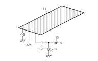
また、図12は例えば「共振周波数切替型逆Fアンテナ」(1997年電子情報通信学会総合大会講演論文集、分冊 通信1、B−1−74、p.74)に示された従来のアンテナ装置を示す構成図であり、図において、11はグランド端子を有する逆Fアンテナ、12,13は逆Fアンテナ11に直列接続されたキャパシタおよびインダクタ、14はそれらキャパシタ12およびインダクタ13の間に接続されたpinダイオードである。
【0003】
次に動作について説明する。
図11および図12は、2共振のアンテナ装置を示したものであり、図11では、電気長の異なる2つの素子アンテナ1,2と、各素子アンテナ1,2の給電部に装荷された2つのトラップ回路5,6とから構成されている。トラップ回路5,6は、一方の素子アンテナが動作しているときに、他方の素子アンテナが動作しないように設計されている。こうすることによって、2つの異なる周波数帯に対して動作するアンテナ装置を実現している。
また、図12は、単共振特性を有する逆Fアンテナ11に、キャパシタ12およびインダクタ13からなる負荷を装荷し、pinダイオード14のオン、オフを利用して負荷の値を変化させることで逆Fアンテナ11の共振周波数を変化させ、これによって複数の周波数帯に対して動作するアンテナ装置を実現している。
【0004】
【発明が解決しようとする課題】
従来のアンテナ装置は以上のように構成されているので、図11に示したアンテナ装置では、素子アンテナ1,2の寸法が大きいため、携帯無線端末機の筐体からアンテナが大きく突き出てしまうという課題があった。
また、図12に示したアンテナ装置では、複数の周波数帯に対して同時に動作することができないという課題があった。
【0005】
この発明は上記のような課題を解決するためになされたもので、複数の周波数帯に対して同時に動作することができると共に、物理的な占有空間を極力小さくして、無線機の筐体から突出しない、または突出量を削減するアンテナ装置を得ることを目的とする。
【0006】
【課題を解決するための手段】
この発明に係るアンテナ装置は、切り欠き部が設けられた有限の大きさを有する地導体と、上記地導体の上方にその地導体と概略平行に設置され、第1の波長に対して共振を発生する電気長を有する第1の放射導体と、上記切り欠き部に上記第1の放射導体に対して概略平行に配置され、第2の波長に対して共振を発生する電気長を有する第3の放射導体と、上記第1の放射導体および上記第3の放射導体とを電気的に接続する導体線とを備え、前記第1の放射導体は、平板状または曲面状に形成されると共に切り欠き部上に配置され、前記第3の放射導体は、地導体と略同一平面に設けられ、上記切り欠き部に形成されたものである。
【0007】
この発明に係るアンテナ装置は、地導体と第3の放射導体が同一基板上にエッチング形成されたものである。
【0018】
【発明の実施の形態】
以下、この発明の実施の一形態を説明する。
実施の形態1.
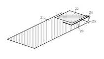
図1はこの発明の実施の形態1によるアンテナ装置を示す構成図であり、図において、21は有限の大きさを有する地導体、22は地導体21の上方にその地導体21と概略平行に設置された平板状または曲面状に形成された放射導体(第1の放射導体)、23は地導体21の上方に放射導体22と概略同一平面上かつ、その放射導体22を取り巻くように設置された屈曲を有する直線状または曲線状に形成された放射導体(第2の放射導体)、24は放射導体22および放射導体23を電気的に接続する導体線、25は放射導体22および放射導体23と地導体21との間から給電する給電点である。
【0019】
次に動作について説明する。
地導体21の上方に、それと概略平行に、周囲長が第1の波長の概略8分の1から1程度の大きさの平板状または曲面状の放射導体22を配置する。この放射導体22の電気長は、所望の周波数f1の波長に対して直列共振を発生するように設定される。例えば、周波数f1の波長の概略4分の1になるように設定する。
また、地導体21の上方に、放射導体22と概略同一平面上かつ、その辺から第1の波長に比べて十分狭い間隙を隔てて、電気長が第2の波長の概略4分の1程度の、屈曲を有する直線状または曲線状の放射導体23を、放射導体22を取り巻くように配置する。この放射導体23の電気長についても、同様に所望の周波数f2の波長に対して直列共振を発生するように設定される。なお、ここでは直列共振を生じさせる長さとして1/4の電気長を記載しているが、これとは異なる長さを有するアンテナの給電部に整合回路を用いることで代用も可能である。例えば、通常第2の波長の2分の1以下の値を設定することが多い。この点、上述の放射導体22についても同様である。また、第2の波長の信号を効率良く送信または受信できる限りにおいて、放射導体22と全く同一平面上に放射導体23を設ける必要はなく、多少の傾き、地導体21に対する高さについて高低の違いがあってもかまわない。
さらに、放射導体22上の一角と放射導体23の一端とを導体線24を介して電気的に接続する。放射導体22上の一角および放射導体23の一端と地導体21との間を給電点25とし、そこに同軸線路、マイクロストリップ線路、トリプレート線路、またはコプレーナ線路等を介して電力を供給する。
但し、地導体21および放射導体22の形状は、動作原理の観点からは必ずしも方形である必要はなく、長方形、台形、または菱形等の多角形、楕円形、またはこれらを変形した形状でも良い。また、放射導体22,23は、電気長に比べて物理長を短くできるヘリカルアンテナのような立体的な形状を用いてもかまわず、メアンダラインアンテナのような平面的なアンテナを用いて、同一プリント基板上に放射導体22,23を配置することもできる。放射導体23は、屈曲を有するものに限らず、整合回路を含めて、アンテナとして動作しうる電気長を有する限り屈曲のない直線状または曲線状の構成をしていても良い。
さらに、放射導体22と放射導体23の地導体21からの高さは、必ずしも同一である必要はないが、これらは地導体21のほぼ投影内に位置するもの、即ち、地導体21より突出しないようにする。この制約は、物理的に小型化を図るという観点からくるものである。従って、小型化する必要がそれほどない場合には、無線機等の筐体から突出しない範囲内であれば、地導体21の投影内から突出してもかまわない。
【0020】
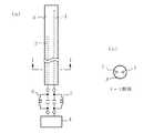
図2はこの発明の実施の形態1によるアンテナ装置の周波数特性を示す特性図であり、図1に示した構造と概略同一のアンテナ装置を実際に試作し、給電点25での反射減衰量の周波数特性を測定した結果を示したものである。2つの周波数帯f1およびf2において反射減衰量が極小になっていることから、試作アンテナ装置は異なる2つの周波数帯に対して同時に動作していることが確認できる。
【0021】
以上のように、この実施の形態1によれば、アンテナ装置を上述のように構成し、放射導体22の大きさと、放射導体23の電気長を、適当に調節することによって、所望の2つの周波数帯に対して同時に動作させることが可能となる。
また、放射導体22と導体線24との接合点を、放射導体22の一角とすることにより、放射導体22を小型化できる。
さらに、放射導体23は、放射導体22を取り巻くように配置し、かつ、放射導体23と放射導体22を共に地導体21のほぼ投影内に配置することによって、アンテナ全体の体積の小形化を図ることが可能となり、無線機等の筐体から突出することのない構成を実現することができる。
【0022】
実施の形態2.
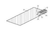
図3はこの発明の実施の形態2によるアンテナ装置を示す構成図であり、図において、31は一角に切り欠き部32が設けられた有限の大きさを有する地導体、33は切り欠き部32に放射導体22に対して概略平行に配置され、螺旋状線状に形成されたヘリカルアンテナ(第3の放射導体)である。なお、導体線24は放射導体22およびヘリカルアンテナ33を電気的に接続し、給電点25は放射導体22およびヘリカルアンテナ33と地導体31との間から給電するようにしたものである。その他の構成は、図1と同等である。
【0023】
次に動作について説明する。
地導体31の一角を切り欠き、切り欠き部32を設ける。地導体31の切り欠き部32に、放射導体22と概略平行になるように、第2の波長の概略4分の1程度の電気長を有する導体線を螺旋状に巻いたヘリカルアンテナ33を配置する。ヘリカルアンテナ33の一端と放射導体22の一角とを導体線24で電気的に接続し、その接続点と地導体31との間の給電点25に同軸線路やマイクロストリップ線路等を介して電力を供給する。このアンテナ装置の基本的な動作原理は、上記実施の形態1に示したものと概ね同一である。
なお、図3では、地導体31の一角に切り欠き部32を設けたが、地導体31の他の位置に切り欠き部を設けてもかまわない。また、放射導体22は、切り欠き部32の真上にある必要はなく、第1の波長を送信または受信できる限りにおいて多少のずれがあってもかまわない。
この実施の形態2では、ヘリカルアンテナ33は切り欠き部32に配置されるため、ヘリカルアンテナ33のように立体的な形状をしているアンテナでも、アンテナ装置全体のスペースを削減することができ、小型化を図ることができる。ここでヘリカルアンテナ33は、地導体31と同一の平面と放射導体22とによって形成される空間内の任意の位置に収納される。
【0024】
以上のように、この実施の形態2によれば、上記実施の形態1に加えて、地導体31の切り欠き部32に、放射導体23に代えたヘリカルアンテナ33を用いることにより、上記実施の形態1のものよりもより一層小形化を図ることが可能となる。
【0025】
実施の形態3.
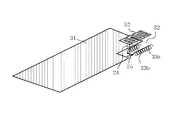
図4はこの発明の実施の形態3によるアンテナ装置を示す構成図であり、図において、36は切り欠き部32に放射導体22に対して概略平行に配置され、線状導体がジグザグに折り曲げられたメアンダラインアンテナ(第3の放射導体)である。その他の構成は、図3と同等である。
【0026】
以上のように、この実施の形態3によれば、上記実施の形態2に加えて、メアンダラインアンテナ36を用いることにより、ヘリカルアンテナ33を用いた場合に比べて、放射導体22との物理的距離を増加させることができる。その結果として、放射導体22およびメアンダラインアンテナ36の動作周波数帯域はより広帯域になる。また、メアンダラインアンテナ36は地導体31と同一平面にあるので、地導体31と共にプリント基板のエッチング加工によって容易に製作できる。
【0027】
実施の形態4.
図5はこの発明の実施の形態4によるアンテナ装置を示す構成図であり、図において、42は実施の形態1から3に示した平板状または曲面状に形成された放射導体22に、1つまたは複数の切り込みを設けた放射導体(第1の放射導体)である。その他の構成は、図3と同等である。
【0028】
以上のように、この実施の形態4によれば、上記実施の形態1から3に加えて、1つまたは複数の切り込みを設けた放射導体42を設けたので、第1の波長に対する放射導体の大きさを小さくすることができ、より一層小型化が可能となる。
【0029】
実施の形態5.
図6はこの発明の実施の形態5によるアンテナ装置を示す構成図であり、図において、33aは地導体31と概略同一平面上になるように切り欠き部32に配置され、第1の波長の概略4分の1程度の電気長を有する導体線を螺旋状に巻いたヘリカルアンテナ(第4の放射導体)、33bは地導体31と概略同一平面上に、かつヘリカルアンテナ33aと互いに概略平行になるように配置され、第2の波長の概略4分の1程度の電気長を有する導体線を螺旋状に巻いたヘリカルアンテナ(第5の放射導体)である。ヘリカルアンテナ33a,33bは共に、地導体の同一の給電点25から給電されるものとする。
【0030】
以上のように、この実施の形態5によれば、上記実施の形態1から4のものに比べて大幅に薄型化を図ることができる。
なお、ヘリカルアンテナ33a,33bの位置関係は、図7に示すように、図6における位置関係と逆であっても構わない。
【0031】
実施の形態6.
図8はこの発明の実施の形態6によるアンテナ装置を示す構成図であり、図において、実施の形態5における2つのヘリカルアンテナ33a,33bのうちの一方(33b)を、地導体31に短絡する。こうすると、ヘリカルアンテナ33bは非励振素子となるが、ヘリカルアンテナ33aとの電磁結合によって励振され、実施の形態5と同様な効果がある。
【0032】
以上のように、この実施の形態6によれば、短絡点の位置に左右されず、給電点25の設計の自由度を高めることが可能となる。
【0033】
実施の形態7.
図9はこの発明の実施の形態7によるアンテナ装置を示す構成図であり、図において、52はヘリカルアンテナ33a,33bの上方に地導体31と概略平行に設置され、電気長が第3の波長の概略4分の1程度になるように平板状または曲面状に形成され、かつ1つまたは複数の切り込みが設けられた放射導体(第6の放射導体)である。放射導体52は導体線24を通じて給電点25から給電されるものである。その他の構成は、図6と同等である。
【0034】
以上のように、この実施の形態7によれば、実施の形態5に加えて3つの異なる周波数帯に対して同時に動作することが可能となる。
【0035】
実施の形態8.
図10はこの発明の実施の形態8によるアンテナ装置を示す構成図であり、図において、53は地導体31の上方に放射導体52と概略同一平面上かつ、その放射導体52を取り巻くように設置され、電気長が第4の波長の概略4分の1程度になるように屈曲を有する直線状または曲線状に形成された放射導体(第7の放射導体)である。放射導体53は、放射導体52と共に導体線24を通じて給電点25から給電されるものである。その他の構成は、図9と同等である。
【0036】
以上のように、この実施の形態8によれば、実施の形態7に加えて4つの異なる周波数帯に対して同時に動作することが可能となる。
【0037】
なお、上記実施の形態1から8では、第1から7の放射導体として特定形状のアンテナを例示したが、この発明はこれらの例に限らず、複数の周波数を適切に送信または受信でき、また、小型化が可能な限りにおいて、様々なタイプのアンテナを使用することができる。例えば、第1から7の放射導体として、平板上アンテナ、ヘリカルアンテナ、メアンダラインアンテナ、平板上アンテナであって1つあるいは複数の切り込みを設けたアンテナ、直線状または曲線状のアンテナを使用することができる。
また、第1から7の放射導体の電気長として概略4分の1を例示したが、この発明はこれらの例に限らず、電気長が所望の波長に対して直列共振を発生するように設定されれば良く、また、この共振の発生は各放射導体に電気的に接続される共振調整回路によって調整しても良い。従って、共振調整回路によって共振点を調整しても、所望の周波数において各放射導体の反射減衰量が極小点近傍となる限り、この発明の効果を損なうものではない。
【0038】
【発明の効果】
以上のように、この発明によれば、切り欠き部が設けられた有限の大きさを有する地導体と、上記地導体の上方にその地導体と概略平行に設置され、第1の波長に対して共振を発生する電気長を有する第1の放射導体と、上記切り欠き部に上記第1の放射導体に対して概略平行に配置され、第2の波長に対して共振を発生する電気長を有する第3の放射導体と、上記第1の放射導体および上記第3の放射導体とを電気的に接続する導体線とを備え、前記第1の放射導体は、平板状または曲面状に形成されると共に切り欠き部上に配置され、前記第3の放射導体は、地導体と略同一平面に設けられ、上記切り欠き部に形成したので、所望の第1の波長および第2の波長に応じて第1の放射導体および第3の放射導体の電気長を調節することによって、2つの周波数帯に対して同時に動作させることができる。
また、アンテナ装置を薄型化することができ、アンテナ装置全体の体積の小形化をさらに図ることができ、無線機等の筐体から突出することのない構成または突出を抑制する構成を実現することができる効果が得られる。
【図面の簡単な説明】
【図1】 この発明の実施の形態1によるアンテナ装置を示す構成図である。
【図2】 この発明の実施の形態1によるアンテナ装置の周波数特性を示す特性図である。
【図3】 この発明の実施の形態2によるアンテナ装置を示す構成図である。
【図4】 この発明の実施の形態3によるアンテナ装置を示す構成図である。
【図5】 この発明の実施の形態4によるアンテナ装置を示す構成図である。
【図6】 この発明の実施の形態5によるアンテナ装置を示す構成図である。
【図7】 この発明の実施の形態5によるアンテナ装置を示す構成図である。
【図8】 この発明の実施の形態6によるアンテナ装置を示す構成図である。
【図9】 この発明の実施の形態7によるアンテナ装置を示す構成図である。
【図10】 この発明の実施の形態8によるアンテナ装置を示す構成図である。
【図11】 従来のアンテナ装置を示す構成図である。
【図12】 従来のアンテナ装置を示す構成図である。
【符号の説明】
21,31 地導体、22,42 放射導体(第1の放射導体)、23 放射導体(第2の放射導体)、24 導体線、25 給電点、32 切り欠き部、33 ヘリカルアンテナ(第3の放射導体)、33a ヘリカルアンテナ(第4の放射導体)、33b ヘリカルアンテナ(第5の放射導体)、36 メアンダラインアンテナ(第3の放射導体)、52 放射導体(第6の放射導体)、53 放射導体(第7の放射導体)。[0001]
BACKGROUND OF THE INVENTION
The present invention relates to an antenna device used in a wireless system such as a mobile phone, PHS, and Bluetooth.
[0002]
[Prior art]
FIG. 11 is a block diagram showing a conventional antenna device disclosed in, for example, Japanese Patent Laid-Open No. 9-46259. In the figure, 1 and 2 are two element antennas having different electrical lengths, 3 is two
FIG. 12 shows a conventional antenna apparatus shown in, for example, “Resonant Frequency Switching Inverted F Antenna” (1997 IEICE General Conference Proceedings,
[0003]
Next, the operation will be described.
FIGS. 11 and 12 show a two-resonance antenna device. In FIG. 11, two
FIG. 12 shows a
[0004]
[Problems to be solved by the invention]
Since the conventional antenna device is configured as described above, in the antenna device shown in FIG. 11, the dimensions of the
Further, the antenna device shown in FIG. 12 has a problem that it cannot operate simultaneously for a plurality of frequency bands.
[0005]
The present invention has been made to solve the above-described problems, and can operate simultaneously with respect to a plurality of frequency bands while reducing the physical occupation space as much as possible from the housing of the radio. An object of the present invention is to obtain an antenna device that does not protrude or reduces the amount of protrusion.
[0006]
[Means for Solving the Problems]
An antenna device according to the present inventionis provided with a ground conductor having a finite size provided with a notch, and is disposed above and in parallel with the ground conductor, and resonates with respect to the first wavelength. A first radiating conductor having an electrical length to be generated, and a third radiating conductor that is disposed substantially parallel to the first radiating conductor in the notch and that generates resonance with respect to the second wavelength. And a conductor wire that electrically connects the first radiation conductor and the third radiation conductor, and the first radiation conductor is formed in a flat plate shape or a curved surface and cut. The third radiating conductor is disposed on the notch and is provided in substantially the same plane as the ground conductor and is formed in the notch .
[0007]
In the antenna device according to the present invention, theground conductor and the third radiating conductor are formed by etching on the same substrate .
[0018]
DETAILED DESCRIPTION OF THE INVENTION
An embodiment of the present invention will be described below.
FIG. 1 is a block diagram showing an antenna apparatus according to
[0019]
Next, the operation will be described.
A flat or curved
In addition, the electrical length is approximately one-fourth of the second wavelength above the
Furthermore, a corner on the
However, the shapes of the
Further, the heights of the
[0020]
FIG. 2 is a characteristic diagram showing the frequency characteristics of the antenna device according to the first embodiment of the present invention. An antenna device substantially identical to the structure shown in FIG. The result of measuring the frequency characteristic is shown. Since the return loss is minimal in the two frequency bands f1 and f2, it can be confirmed that the prototype antenna apparatus is operating simultaneously in two different frequency bands.
[0021]
As described above, according to the first embodiment, the antenna device is configured as described above, and by appropriately adjusting the size of the radiating
Moreover, the
Further, the radiating
[0022]
3 is a block diagram showing an antenna apparatus according to
[0023]
Next, the operation will be described.
A corner of the
In FIG. 3, the
In the second embodiment, since the
[0024]
As described above, according to the second embodiment, in addition to the first embodiment, the
[0025]
FIG. 4 is a block diagram showing an antenna apparatus according to
[0026]
As described above, according to the third embodiment, by using the
[0027]
FIG. 5 is a block diagram showing an antenna apparatus according to
[0028]
As described above, according to the fourth embodiment, in addition to the first to third embodiments, since the
[0029]
Embodiment 5 FIG.
FIG. 6 is a block diagram showing an antenna apparatus according to Embodiment 5 of the present invention. In the figure, 33a is arranged in the
[0030]
As described above, according to the fifth embodiment, the thickness can be significantly reduced as compared with the first to fourth embodiments.
The positional relationship between the
[0031]
Embodiment 6 FIG.
FIG. 8 is a block diagram showing an antenna apparatus according to Embodiment 6 of the present invention. In the figure, one (33b) of the two
[0032]
As described above, according to the sixth embodiment, the design flexibility of the
[0033]
Embodiment 7 FIG.
FIG. 9 is a block diagram showing an antenna apparatus according to Embodiment 7 of the present invention. In the figure, 52 is installed above the
[0034]
As described above, according to the seventh embodiment, it is possible to simultaneously operate for three different frequency bands in addition to the fifth embodiment.
[0035]
Embodiment 8 FIG.
FIG. 10 is a block diagram showing an antenna apparatus according to Embodiment 8 of the present invention. In the figure, 53 is installed above the
[0036]
As described above, according to the eighth embodiment, it is possible to simultaneously operate on four different frequency bands in addition to the seventh embodiment.
[0037]
In the first to eighth embodiments, the antenna having a specific shape is exemplified as the first to seventh radiation conductors. However, the present invention is not limited to these examples, and a plurality of frequencies can be appropriately transmitted or received. As long as downsizing is possible, various types of antennas can be used. For example, as the first to seventh radiating conductors, a flat antenna, a helical antenna, a meander line antenna, a flat antenna that has one or a plurality of cuts, and a linear or curved antenna is used. Can do.
In addition, the electric length of the first to seventh radiating conductors is exemplified by about a quarter, but the present invention is not limited to these examples, and the electric length is set so as to generate series resonance with respect to a desired wavelength. The occurrence of this resonance may be adjusted by a resonance adjustment circuit electrically connected to each radiation conductor. Therefore, even if the resonance point is adjusted by the resonance adjustment circuit, the effect of the present invention is not impaired as long as the reflection attenuation amount of each radiation conductor is near the minimum point at a desired frequency.
[0038]
【The invention's effect】
As described above, according to the present invention,a ground conductor having a finite size provided with a notch ,and a ground conductor disposed above and in parallel with the ground conductor, the first wavelength is A first radiating conductor having an electrical length that generates resonance, and an electrical length that is arranged substantially parallel to the first radiating conductor in the notch and that generates resonance with respect to the second wavelength. A third radiation conductor and a conductor wire that electrically connects the first radiation conductor and the third radiation conductor, and the first radiation conductor is formed in a flat plate shape or a curved surface shape. And the third radiating conductor is provided in substantially the same plane as the ground conductor and is formed in the notched portion, so that it corresponds to the desired first wavelength and second wavelength. By adjusting the electrical length of the first and third radiating conductors Te can be operated simultaneously for the two frequency bands.
In addition, the antenna device can be thinned, the volume of the entire antenna devicecan be further reduced, and a structure that does not protrude from a housing such as a wireless device or a structure that suppresses the protrusion is realized. The effect that can be obtained.
[Brief description of the drawings]
FIG. 1 is a configuration diagram illustrating an antenna device according to a first embodiment of the present invention.
FIG. 2 is a characteristic diagram showing frequency characteristics of the antenna device according to the first embodiment of the present invention.
FIG. 3 is a block diagram showing an antenna apparatus according to
FIG. 4 is a block diagram showing an antenna apparatus according to
FIG. 5 is a block diagram showing an antenna apparatus according to
FIG. 6 is a block diagram showing an antenna apparatus according to a fifth embodiment of the present invention.
FIG. 7 is a block diagram showing an antenna apparatus according to Embodiment 5 of the present invention.
FIG. 8 is a block diagram showing an antenna apparatus according to a sixth embodiment of the present invention.
FIG. 9 is a block diagram showing an antenna apparatus according to a seventh embodiment of the present invention.
FIG. 10 is a block diagram showing an antenna apparatus according to an eighth embodiment of the present invention.
FIG. 11 is a block diagram showing a conventional antenna device.
FIG. 12 is a block diagram showing a conventional antenna device.
[Explanation of symbols]
21, 31 Ground conductor, 22, 42 Radiation conductor (first radiation conductor), 23 Radiation conductor (second radiation conductor), 24 Conductor wire, 25 Feed point, 32 Notch, 33 Helical antenna (3rd Radiation conductor), 33a helical antenna (fourth radiation conductor), 33b helical antenna (fifth radiation conductor), 36 meander line antenna (third radiation conductor), 52 radiation conductor (sixth radiation conductor), 53 Radiation conductor (seventh radiation conductor).
Claims (2)
Translated fromJapanese前記第1の放射導体は、平板状または曲面状に形成されると共に切り欠き部上に配置され、前記第3の放射導体は、地導体と略同一平面に設けられ、上記切り欠き部に形成されたことを特徴とするアンテナ装置。The has a ground conductor having a finite size which notches are provided, disposed parallel the land conductor and outlined above the ground conductor, an electrical length which generates aresonance with respect to the first wavelength and first radiating conductor, arranged in parallel with schematic with respect to the first radiation conductor to the cutout portion, and a third radiation conductor having an electrical length which generates aresonance with respect to the second wavelength, the A conductor wire that electrically connects the first radiation conductor and the third radiation conductor;
The first radiating conductor is formed in a flat plate shape or a curved surface and is disposed on the notch, and the third radiating conductor is provided in substantially the same plane as the ground conductor and is formed in the notch. An antenna devicecharacterized by the above .
Priority Applications (1)
| Application Number | Priority Date | Filing Date | Title |
|---|---|---|---|
| JP2000365819AJP3730112B2 (en) | 2000-11-30 | 2000-11-30 | Antenna device |
Applications Claiming Priority (1)
| Application Number | Priority Date | Filing Date | Title |
|---|---|---|---|
| JP2000365819AJP3730112B2 (en) | 2000-11-30 | 2000-11-30 | Antenna device |
Publications (2)
| Publication Number | Publication Date |
|---|---|
| JP2002171126A JP2002171126A (en) | 2002-06-14 |
| JP3730112B2true JP3730112B2 (en) | 2005-12-21 |
Family
ID=18836528
Family Applications (1)
| Application Number | Title | Priority Date | Filing Date |
|---|---|---|---|
| JP2000365819AExpired - Fee RelatedJP3730112B2 (en) | 2000-11-30 | 2000-11-30 | Antenna device |
Country Status (1)
| Country | Link |
|---|---|
| JP (1) | JP3730112B2 (en) |
Families Citing this family (17)
| Publication number | Priority date | Publication date | Assignee | Title |
|---|---|---|---|---|
| EP1569299B1 (en) | 2002-11-27 | 2008-10-22 | Taiyo Yuden Co., Ltd. | Antenna, dielectric substrate for antenna, radio communication card |
| JP2004328693A (en) | 2002-11-27 | 2004-11-18 | Taiyo Yuden Co Ltd | Antenna and dielectric substrate for antenna |
| JP4170828B2 (en) | 2002-11-27 | 2008-10-22 | 太陽誘電株式会社 | Antenna and dielectric substrate for antenna |
| JP2004328694A (en) | 2002-11-27 | 2004-11-18 | Taiyo Yuden Co Ltd | Antenna and wireless communication card |
| JP2004328703A (en) | 2002-11-27 | 2004-11-18 | Taiyo Yuden Co Ltd | Antenna |
| WO2005004282A1 (en)* | 2003-07-04 | 2005-01-13 | Mitsubishi Denki Kabushiki Kaisha | Antenna element and mobile telephone device |
| US7592958B2 (en)* | 2003-10-22 | 2009-09-22 | Sony Ericsson Mobile Communications, Ab | Multi-band antennas and radio apparatus incorporating the same |
| JP4439998B2 (en)* | 2004-04-09 | 2010-03-24 | パナソニック株式会社 | Antenna for portable radio |
| EP1703587A4 (en)* | 2004-04-27 | 2007-04-11 | Murata Manufacturing Co | Antenna and portable radio communication unit |
| JP2006025015A (en)* | 2004-07-06 | 2006-01-26 | Kyocera Corp | Mobile communication terminal |
| JP2006080721A (en)* | 2004-09-08 | 2006-03-23 | Nec Corp | Antenna device and portable radio device |
| WO2007020728A1 (en)* | 2005-08-12 | 2007-02-22 | Murata Manufacturing Co., Ltd. | Antenna structure and wireless communication apparatus provided with same |
| US7443350B2 (en)* | 2006-07-07 | 2008-10-28 | International Business Machines Corporation | Embedded multi-mode antenna architectures for wireless devices |
| JP4962723B2 (en)* | 2007-02-20 | 2012-06-27 | ミツミ電機株式会社 | Antenna element and broadband antenna device |
| JP4124802B1 (en)* | 2007-10-30 | 2008-07-23 | 松下電器産業株式会社 | Portable wireless device |
| JP4707728B2 (en)* | 2008-03-28 | 2011-06-22 | パナソニック株式会社 | Portable wireless device |
| JP5189004B2 (en)* | 2009-01-29 | 2013-04-24 | 株式会社フジクラ | Monopole antenna |
- 2000
- 2000-11-30JPJP2000365819Apatent/JP3730112B2/ennot_activeExpired - Fee Related
Also Published As
| Publication number | Publication date |
|---|---|
| JP2002171126A (en) | 2002-06-14 |
Similar Documents
| Publication | Publication Date | Title |
|---|---|---|
| JP3730112B2 (en) | Antenna device | |
| JP3114605B2 (en) | Surface mount antenna and communication device using the same | |
| US7755545B2 (en) | Antenna and method of manufacturing the same, and portable wireless terminal using the same | |
| EP1198027B1 (en) | Small antenna | |
| JP3340374B2 (en) | Multi-frequency antenna | |
| US6498586B2 (en) | Method for coupling a signal and an antenna structure | |
| JP4109629B2 (en) | RF-MEMs tuned slot antenna and manufacturing method thereof | |
| US7339531B2 (en) | Multi frequency magnetic dipole antenna structures and method of reusing the volume of an antenna | |
| US20060071857A1 (en) | Planar high-frequency or microwave antenna | |
| US7250909B2 (en) | Antenna and method of making the same | |
| CN1185762C (en) | Multiband Antennas for Communication Terminal Devices | |
| JP2004088218A (en) | Planar antenna | |
| JPH11150415A (en) | Multi-frequency antenna | |
| US20070057849A1 (en) | Antenna for dual band operation | |
| JP2000022421A (en) | Chip antenna and radio device mounted with it | |
| KR20030007718A (en) | Internal multi-band antennas for mobile communications | |
| KR20050086733A (en) | Antenna for plurality of bands | |
| JP2002185231A (en) | Small-sized microwave antenna | |
| US7030833B2 (en) | Antenna device | |
| WO2001076007A1 (en) | Wide beamwidth ultra-compact antenna with multiple polarization | |
| US6982673B2 (en) | Inverted-F metal plate antenna having increased bandwidth | |
| JP2002359515A (en) | M-type antenna device | |
| JP3114836B2 (en) | Printed dipole antenna | |
| KR101097950B1 (en) | A small antenna and a multiband antenna | |
| WO2004025781A1 (en) | Loop antenna |
Legal Events
| Date | Code | Title | Description |
|---|---|---|---|
| A977 | Report on retrieval | Free format text:JAPANESE INTERMEDIATE CODE: A971007 Effective date:20050310 | |
| A131 | Notification of reasons for refusal | Free format text:JAPANESE INTERMEDIATE CODE: A131 Effective date:20050322 | |
| A521 | Written amendment | Free format text:JAPANESE INTERMEDIATE CODE: A523 Effective date:20050520 | |
| TRDD | Decision of grant or rejection written | ||
| A01 | Written decision to grant a patent or to grant a registration (utility model) | Free format text:JAPANESE INTERMEDIATE CODE: A01 Effective date:20050906 | |
| A61 | First payment of annual fees (during grant procedure) | Free format text:JAPANESE INTERMEDIATE CODE: A61 Effective date:20051005 | |
| R150 | Certificate of patent or registration of utility model | Free format text:JAPANESE INTERMEDIATE CODE: R150 | |
| FPAY | Renewal fee payment (event date is renewal date of database) | Free format text:PAYMENT UNTIL: 20091014 Year of fee payment:4 | |
| FPAY | Renewal fee payment (event date is renewal date of database) | Free format text:PAYMENT UNTIL: 20091014 Year of fee payment:4 | |
| FPAY | Renewal fee payment (event date is renewal date of database) | Free format text:PAYMENT UNTIL: 20101014 Year of fee payment:5 | |
| FPAY | Renewal fee payment (event date is renewal date of database) | Free format text:PAYMENT UNTIL: 20111014 Year of fee payment:6 | |
| FPAY | Renewal fee payment (event date is renewal date of database) | Free format text:PAYMENT UNTIL: 20121014 Year of fee payment:7 | |
| LAPS | Cancellation because of no payment of annual fees |