JP3727878B2 - Metal film production equipment - Google Patents
Metal film production equipmentDownload PDFInfo
- Publication number
- JP3727878B2 JP3727878B2JP2001348315AJP2001348315AJP3727878B2JP 3727878 B2JP3727878 B2JP 3727878B2JP 2001348315 AJP2001348315 AJP 2001348315AJP 2001348315 AJP2001348315 AJP 2001348315AJP 3727878 B2JP3727878 B2JP 3727878B2
- Authority
- JP
- Japan
- Prior art keywords
- etched
- chamber
- plasma
- substrate
- source gas
- Prior art date
- Legal status (The legal status is an assumption and is not a legal conclusion. Google has not performed a legal analysis and makes no representation as to the accuracy of the status listed.)
- Expired - Fee Related
Links
- 229910052751metalInorganic materials0.000titleclaimsdescription165
- 239000002184metalSubstances0.000titleclaimsdescription165
- 238000004519manufacturing processMethods0.000titleclaimsdescription78
- 239000000758substrateSubstances0.000claimsdescription157
- 239000002243precursorSubstances0.000claimsdescription79
- 229910052736halogenInorganic materials0.000claimsdescription69
- 239000000460chlorineSubstances0.000claimsdescription50
- 150000002367halogensChemical class0.000claimsdescription47
- 239000010949copperSubstances0.000claimsdescription37
- 238000005530etchingMethods0.000claimsdescription34
- 239000002994raw materialSubstances0.000claimsdescription28
- 238000006722reduction reactionMethods0.000claimsdescription26
- 230000005611electricityEffects0.000claimsdescription20
- RYGMFSIKBFXOCR-UHFFFAOYSA-NCopperChemical compound[Cu]RYGMFSIKBFXOCR-UHFFFAOYSA-N0.000claimsdescription19
- 229910052802copperInorganic materials0.000claimsdescription19
- 239000011810insulating materialSubstances0.000claimsdescription19
- 238000000034methodMethods0.000claimsdescription8
- ZAMOUSCENKQFHK-UHFFFAOYSA-NChlorine atomChemical compound[Cl]ZAMOUSCENKQFHK-UHFFFAOYSA-N0.000claimsdescription7
- 229910052801chlorineInorganic materials0.000claimsdescription7
- 229910052715tantalumInorganic materials0.000claimsdescription7
- 229910052719titaniumInorganic materials0.000claimsdescription7
- 239000010936titaniumSubstances0.000claimsdescription7
- 229910052721tungstenInorganic materials0.000claimsdescription7
- RTAQQCXQSZGOHL-UHFFFAOYSA-NTitaniumChemical compound[Ti]RTAQQCXQSZGOHL-UHFFFAOYSA-N0.000claimsdescription4
- 150000004820halidesChemical class0.000claimsdescription4
- GUVRBAGPIYLISA-UHFFFAOYSA-Ntantalum atomChemical compound[Ta]GUVRBAGPIYLISA-UHFFFAOYSA-N0.000claimsdescription4
- WFKWXMTUELFFGS-UHFFFAOYSA-NtungstenChemical compound[W]WFKWXMTUELFFGS-UHFFFAOYSA-N0.000claimsdescription4
- 239000010937tungstenSubstances0.000claimsdescription4
- 239000007789gasSubstances0.000description165
- 239000010408filmSubstances0.000description105
- 239000004020conductorSubstances0.000description16
- 238000006243chemical reactionMethods0.000description11
- 239000010409thin filmSubstances0.000description11
- 229910052756noble gasInorganic materials0.000description10
- 230000002093peripheral effectEffects0.000description9
- 239000012535impuritySubstances0.000description8
- 230000015572biosynthetic processEffects0.000description6
- 150000002500ionsChemical class0.000description5
- KZBUYRJDOAKODT-UHFFFAOYSA-NChlorineChemical compoundClClKZBUYRJDOAKODT-UHFFFAOYSA-N0.000description4
- 239000000919ceramicSubstances0.000description3
- 229910052737goldInorganic materials0.000description3
- 238000005192partitionMethods0.000description3
- 229910052697platinumInorganic materials0.000description3
- 229910052709silverInorganic materials0.000description3
- 230000006641stabilisationEffects0.000description3
- 238000011105stabilizationMethods0.000description3
- 230000000694effectsEffects0.000description2
- GCSJLQSCSDMKTP-UHFFFAOYSA-Nethenyl(trimethyl)silaneChemical compoundC[Si](C)(C)C=CGCSJLQSCSDMKTP-UHFFFAOYSA-N0.000description2
- 239000003507refrigerantSubstances0.000description2
- 238000007740vapor depositionMethods0.000description2
- ZCYVEMRRCGMTRW-UHFFFAOYSA-N7553-56-2Chemical compound[I]ZCYVEMRRCGMTRW-UHFFFAOYSA-N0.000description1
- WKBOTKDWSSQWDR-UHFFFAOYSA-NBromine atomChemical compound[Br]WKBOTKDWSSQWDR-UHFFFAOYSA-N0.000description1
- VEXZGXHMUGYJMC-UHFFFAOYSA-MChloride anionChemical compound[Cl-]VEXZGXHMUGYJMC-UHFFFAOYSA-M0.000description1
- PXGOKWXKJXAPGV-UHFFFAOYSA-NFluorineChemical compoundFFPXGOKWXKJXAPGV-UHFFFAOYSA-N0.000description1
- 229910052782aluminiumInorganic materials0.000description1
- XAGFODPZIPBFFR-UHFFFAOYSA-NaluminiumChemical compound[Al]XAGFODPZIPBFFR-UHFFFAOYSA-N0.000description1
- GDTBXPJZTBHREO-UHFFFAOYSA-NbromineSubstancesBrBrGDTBXPJZTBHREO-UHFFFAOYSA-N0.000description1
- 229910052794bromiumInorganic materials0.000description1
- 238000007796conventional methodMethods0.000description1
- 150000004696coordination complexChemical class0.000description1
- 230000007423decreaseEffects0.000description1
- 230000003247decreasing effectEffects0.000description1
- 238000009826distributionMethods0.000description1
- 229910052731fluorineInorganic materials0.000description1
- 239000011737fluorineSubstances0.000description1
- 125000005843halogen groupChemical group0.000description1
- 230000006698inductionEffects0.000description1
- 229910052740iodineInorganic materials0.000description1
- 239000011630iodineSubstances0.000description1
- 239000007788liquidSubstances0.000description1
- 239000000463materialSubstances0.000description1
- 125000002524organometallic groupChemical group0.000description1
- 239000007787solidSubstances0.000description1
- 239000002904solventSubstances0.000description1
Images


Classifications
- H—ELECTRICITY
- H01—ELECTRIC ELEMENTS
- H01J—ELECTRIC DISCHARGE TUBES OR DISCHARGE LAMPS
- H01J37/00—Discharge tubes with provision for introducing objects or material to be exposed to the discharge, e.g. for the purpose of examination or processing thereof
- H01J37/32—Gas-filled discharge tubes
- H01J37/32009—Arrangements for generation of plasma specially adapted for examination or treatment of objects, e.g. plasma sources
- H01J37/32082—Radio frequency generated discharge
- H01J37/321—Radio frequency generated discharge the radio frequency energy being inductively coupled to the plasma
- C—CHEMISTRY; METALLURGY
- C23—COATING METALLIC MATERIAL; COATING MATERIAL WITH METALLIC MATERIAL; CHEMICAL SURFACE TREATMENT; DIFFUSION TREATMENT OF METALLIC MATERIAL; COATING BY VACUUM EVAPORATION, BY SPUTTERING, BY ION IMPLANTATION OR BY CHEMICAL VAPOUR DEPOSITION, IN GENERAL; INHIBITING CORROSION OF METALLIC MATERIAL OR INCRUSTATION IN GENERAL
- C23C—COATING METALLIC MATERIAL; COATING MATERIAL WITH METALLIC MATERIAL; SURFACE TREATMENT OF METALLIC MATERIAL BY DIFFUSION INTO THE SURFACE, BY CHEMICAL CONVERSION OR SUBSTITUTION; COATING BY VACUUM EVAPORATION, BY SPUTTERING, BY ION IMPLANTATION OR BY CHEMICAL VAPOUR DEPOSITION, IN GENERAL
- C23C16/00—Chemical coating by decomposition of gaseous compounds, without leaving reaction products of surface material in the coating, i.e. chemical vapour deposition [CVD] processes
- C23C16/06—Chemical coating by decomposition of gaseous compounds, without leaving reaction products of surface material in the coating, i.e. chemical vapour deposition [CVD] processes characterised by the deposition of metallic material
- C23C16/08—Chemical coating by decomposition of gaseous compounds, without leaving reaction products of surface material in the coating, i.e. chemical vapour deposition [CVD] processes characterised by the deposition of metallic material from metal halides
- C23C16/14—Deposition of only one other metal element
- C—CHEMISTRY; METALLURGY
- C23—COATING METALLIC MATERIAL; COATING MATERIAL WITH METALLIC MATERIAL; CHEMICAL SURFACE TREATMENT; DIFFUSION TREATMENT OF METALLIC MATERIAL; COATING BY VACUUM EVAPORATION, BY SPUTTERING, BY ION IMPLANTATION OR BY CHEMICAL VAPOUR DEPOSITION, IN GENERAL; INHIBITING CORROSION OF METALLIC MATERIAL OR INCRUSTATION IN GENERAL
- C23C—COATING METALLIC MATERIAL; COATING MATERIAL WITH METALLIC MATERIAL; SURFACE TREATMENT OF METALLIC MATERIAL BY DIFFUSION INTO THE SURFACE, BY CHEMICAL CONVERSION OR SUBSTITUTION; COATING BY VACUUM EVAPORATION, BY SPUTTERING, BY ION IMPLANTATION OR BY CHEMICAL VAPOUR DEPOSITION, IN GENERAL
- C23C16/00—Chemical coating by decomposition of gaseous compounds, without leaving reaction products of surface material in the coating, i.e. chemical vapour deposition [CVD] processes
- C23C16/44—Chemical coating by decomposition of gaseous compounds, without leaving reaction products of surface material in the coating, i.e. chemical vapour deposition [CVD] processes characterised by the method of coating
- C23C16/448—Chemical coating by decomposition of gaseous compounds, without leaving reaction products of surface material in the coating, i.e. chemical vapour deposition [CVD] processes characterised by the method of coating characterised by the method used for generating reactive gas streams, e.g. by evaporation or sublimation of precursor materials
- C23C16/4488—Chemical coating by decomposition of gaseous compounds, without leaving reaction products of surface material in the coating, i.e. chemical vapour deposition [CVD] processes characterised by the method of coating characterised by the method used for generating reactive gas streams, e.g. by evaporation or sublimation of precursor materials by in situ generation of reactive gas by chemical or electrochemical reaction
- C—CHEMISTRY; METALLURGY
- C23—COATING METALLIC MATERIAL; COATING MATERIAL WITH METALLIC MATERIAL; CHEMICAL SURFACE TREATMENT; DIFFUSION TREATMENT OF METALLIC MATERIAL; COATING BY VACUUM EVAPORATION, BY SPUTTERING, BY ION IMPLANTATION OR BY CHEMICAL VAPOUR DEPOSITION, IN GENERAL; INHIBITING CORROSION OF METALLIC MATERIAL OR INCRUSTATION IN GENERAL
- C23C—COATING METALLIC MATERIAL; COATING MATERIAL WITH METALLIC MATERIAL; SURFACE TREATMENT OF METALLIC MATERIAL BY DIFFUSION INTO THE SURFACE, BY CHEMICAL CONVERSION OR SUBSTITUTION; COATING BY VACUUM EVAPORATION, BY SPUTTERING, BY ION IMPLANTATION OR BY CHEMICAL VAPOUR DEPOSITION, IN GENERAL
- C23C16/00—Chemical coating by decomposition of gaseous compounds, without leaving reaction products of surface material in the coating, i.e. chemical vapour deposition [CVD] processes
- C23C16/44—Chemical coating by decomposition of gaseous compounds, without leaving reaction products of surface material in the coating, i.e. chemical vapour deposition [CVD] processes characterised by the method of coating
- C23C16/455—Chemical coating by decomposition of gaseous compounds, without leaving reaction products of surface material in the coating, i.e. chemical vapour deposition [CVD] processes characterised by the method of coating characterised by the method used for introducing gases into reaction chamber or for modifying gas flows in reaction chamber
- H—ELECTRICITY
- H01—ELECTRIC ELEMENTS
- H01J—ELECTRIC DISCHARGE TUBES OR DISCHARGE LAMPS
- H01J2237/00—Discharge tubes exposing object to beam, e.g. for analysis treatment, etching, imaging
- H01J2237/20—Positioning, supporting, modifying or maintaining the physical state of objects being observed or treated
- H01J2237/2001—Maintaining constant desired temperature
Landscapes
- Chemical & Material Sciences (AREA)
- Engineering & Computer Science (AREA)
- General Chemical & Material Sciences (AREA)
- Metallurgy (AREA)
- Materials Engineering (AREA)
- Mechanical Engineering (AREA)
- Chemical Kinetics & Catalysis (AREA)
- Organic Chemistry (AREA)
- Electrochemistry (AREA)
- Physics & Mathematics (AREA)
- Plasma & Fusion (AREA)
- Analytical Chemistry (AREA)
- Chemical Vapour Deposition (AREA)
- Electrodes Of Semiconductors (AREA)
Description
Translated fromJapanese【0001】
【発明の属する技術分野】
本発明は、気相成長法により基板の表面に金属膜を作製する金属膜作製装置及び金属膜作製方法に関する。
【0002】
【従来の技術】
従来、気相成長法により金属膜、例えば、銅の薄膜を作製する場合、例えば、銅・ヘキサフロロアセチルアセトナト・トリメチルビニルシラン等の液体の有機金属錯体を原料として用い、固体状の原料を溶媒に溶かし、熱的な反応を利用して気化して基板に成膜を実施している。
【0003】
【発明が解決しようとする課題】
従来の技術では、熱的反応を利用した成膜のため、成膜速度の向上を図ることが困難であった。また、原料となる金属錯体が高価であり、しかも、銅に付随しているヘキサフロロアセチルアセトナト及びトリメチルビニルシランが銅の薄膜中に不純物として残留するため、膜質の向上を図ることが困難であった。
【0004】
本発明は上記状況に鑑みてなされたもので、成膜速度が速く、安価な原料を用いることができ、膜中に不純物が残留しない金属膜作製装置及び金属膜作製方法を提供することを目的とする。
【0005】
【課題を解決するための手段】
上記目的を達成するための本発明の金属膜作製装置の構成は、基板を収容するチャンバと、チャンバ内にハロゲンと希ガスからなる原料ガスを供給する原料ガス供給手段と、チャンバ内に原料ガスプラズマを発生させて、原料ガスプラズマで被エッチング部材をエッチングすることにより、被エッチング部材に含まれる金属成分とハロゲンとの前駆体を生成するプラズマ発生手段と、基板側の温度を被エッチング部材側の温度よりも低くする温度制御手段とを備え、前記前駆体が基板に運ばれる過程において、該前駆体中のハロゲン同士の還元反応により、該前駆体から金属成分のみを生成し、該金属成分のみを前記基板に成膜させるようにしたことを特徴とする。
上記目的を達成するための本発明の金属膜作製装置の構成は、基板が収容され上部が開口されたチャンバと、チャンバ内にハロゲンと希ガスからなる原料ガスを供給する原料ガス供給手段と、チャンバの上部の開口を密閉する絶縁材製の天井部材と、天井部材の外方に設けられチャンバの内部を給電によりプラズマ化するためのアンテナ部材と、アンテナ部材の電気の流れ方向に対して不連続状態で基板と天井部材との間に複数配置される金属製の被エッチング部材と、アンテナ部材に給電を行い被エッチング部材の基板側にアンテナ部材の電気の流れ方向と同一方向の電気の流れを生じさせることによりチャンバの内部をプラズマ化して原料ガスプラズマを発生させ原料ガスプラズマで被エッチング部材をエッチングすることにより被エッチング部材に含まれる金属成分とハロゲンとの前駆体を生成するプラズマ発生手段と、基板側の温度を被エッチング部材側の温度よりも低くして前駆体の金属成分をハロゲンの還元により基板に成膜させる温度制御手段とを備えたことを特徴とする。
【0006】
また、上記目的を達成するための本発明の金属膜作製装置の構成は、基板が収容されると共に一端側が開口する円筒状のチャンバと、チャンバの開口を密閉する絶縁材製の円盤状の天井部材と、チャンバ内にハロゲンと希ガスからなる原料ガスを供給する原料ガス供給手段と、天井部材の外方に設けられチャンバの内部を給電によりプラズマ化するための平面リング形状のアンテナ部材と、基板と天井部材との間におけるチャンバの径方向に延びると共に周方向に複数配置されアンテナ部材の電気の流れ方向に対して不連続状態となる金属製の被エッチング部材と、アンテナ部材に給電を行い被エッチング部材の基板側にアンテナ部材の電気の流れ方向と同一方向の電気の流れを生じさせることでチャンバの内部をプラズマ化して原料ガスプラズマを発生させ原料ガスプラズマで被エッチング部材をエッチングすることにより被エッチング部材に含まれる金属成分とハロゲンとの前駆体を生成するプラズマ発生手段と、基板側の温度を被エッチング部材側の温度よりも低くして前駆体の金属成分をハロゲンの還元により基板に成膜させる温度制御手段とを備えたことを特徴とする。
【0007】
また、上記目的を達成するための本発明の金属膜作製装置の構成は、基板が収容されると共に一端側が開口する円筒状のチャンバと、チャンバの開口を密閉する絶縁材製の外方側に湾曲した凸形状の天井部材と、チャンバ内にハロゲンと希ガスからなる原料ガスを供給する原料ガス供給手段と、天井部材の外方周囲に設けられチャンバの内部を給電によりプラズマ化するための円錐リング状のアンテナ部材と、基板と天井部材との間におけるチャンバの径方向に延びると共に周方向に複数配置されアンテナ部材の電気の流れ方向に対して不連続状態となる金属製の被エッチング部材と、アンテナ部材に給電を行い被エッチング部材の基板側にアンテナ部材の電気の流れ方向と同一方向の電気の流れを生じさせることでチャンバの内部をプラズマ化して原料ガスプラズマを発生させ原料ガスプラズマで被エッチング部材をエッチングすることにより被エッチング部材に含まれる金属成分とハロゲンとの前駆体を生成するプラズマ発生手段と、基板側の温度を被エッチング部材側の温度よりも低くして前駆体の金属成分をハロゲンの還元により基板に成膜させる温度制御手段とを備えたことを特徴とする。
【0008】
また、上記目的を達成するための本発明の金属膜作製装置の構成は、基板が収容されると共に一端側が開口する円筒状のチャンバと、チャンバの開口を密閉する絶縁材製の円盤状の天井部材と、チャンバの一端側に設けられる絶縁材製の筒部と、チャンバ内にハロゲンと希ガスからなる原料ガスを供給する原料ガス供給手段と、天井部材の外方に設けられチャンバの内部を給電によりプラズマ化するための平面リング形状のアンテナ部材と、筒部の周囲に設けられチャンバの内部を給電によりプラズマ化するための円筒コイル状のコイルアンテナ部材と、基板と天井部材との間におけるチャンバの径方向に延びると共に周方向に複数配置されアンテナ部材及びコイルアンテナ部材の電気の流れ方向に対して不連続状態となる金属製の被エッチング部材と、アンテナ部材及びコイルアンテナ部材に給電を行い被エッチング部材の反アンテナ側にアンテナ部材の電気の流れ方向と同一方向の電気の流れを生じさせることでチャンバの内部をプラズマ化して原料ガスプラズマを発生させ原料ガスプラズマで被エッチング部材をエッチングすることにより被エッチング部材に含まれる金属成分とハロゲンとの前駆体を生成するプラズマ発生手段と、基板側の温度を被エッチング部材側の温度よりも低くして前駆体の金属成分をハロゲンの還元により基板に成膜させる温度制御手段とを備えたことを特徴とする。
【0009】
そして、複数の被エッチング部材を電気的につないで同電位にする同電位維持手段を備えたことをを特徴とする。また、温度制御手段は、被エッチング部材に設けられ被エッチング部材を基板側の温度よりも高温に保持する手段であることを特徴とする。また、原料ガス供給手段は、被エッチング部材に設けられたガス供給通路及びガス供給通路に連通するガス噴出穴であることを特徴とする。
【0010】
また、被エッチング部材の基板側の面に表面が凹側に不連続となる凹部を形成したことを特徴とする。また、ハロゲンと希ガスからなる原料ガスは、塩素を含有する原料ガスであることを特徴とする。また、被エッチング部材を銅製とすることにより、前駆体としてCuxClyを生成することを特徴とする。また、被エッチング部材は、ハロゲン化物形成金属であるタンタルもしくはタングステンもしくはチタンであることを特徴とする。
【0011】
上記目的を達成するための本発明の金属膜作製方法は、基板をチャンバ内に収容し、チャンバ内にハロゲンと希ガスからなる原料ガスを供給し、チャンバ内に原料ガスプラズマを発生させて、原料ガスプラズマで被エッチング部材をエッチングすることにより、被エッチング部材に含まれる金属成分とハロゲンとの前駆体を生成し、基板側の温度を被エッチング部材側の温度よりも低くして、前記前駆体が基板に運ばれる過程において、該前駆体中のハロゲン同士の還元反応により、該前駆体から金属成分のみを生成し、該金属成分のみを前記基板に成膜させることを特徴とする。
上記目的を達成するための本発明の金属膜作製方法は、アンテナ部材により基板が収容されたチャンバの内部を給電によりプラズマ化するに際し、アンテナ部材の電気の流れ方向に対して不連続状態で複数の金属製の被エッチング部材を配置し、アンテナ部材に給電を行い被エッチング部材の基板側にアンテナ部材の電気の流れ方向と同一方向の電気の流れを生じさせることによりチャンバの内部をプラズマ化してハロゲンと希ガスからなる原料ガスプラズマを発生させ原料ガスプラズマで被エッチング部材をエッチングすることにより被エッチング部材に含まれる金属成分とハロゲンとの前駆体を生成し、基板側の温度を被エッチング部材側の温度よりも低くして前駆体の金属成分をハロゲンの還元により基板に成膜させることを特徴とする。
【0012】
そして、ハロゲンと希ガスからなる原料ガスは、塩素を含有する原料ガスであることを特徴とする。また、被エッチング部材を銅製とすることにより、前駆体としてCuxClyを生成することを特徴とする。また、被エッチング部材は、ハロゲン化物形成金属であるタンタルもしくはタングステンもしくはチタンであることを特徴とする。
【0013】
【発明の実施の形態】
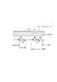
図1乃至図3に基づいて本発明の金属膜作製装置及び金属膜作製方法の第1実施形態例を説明する。図1には本発明の第1実施形態例に係る金属膜作製方法を実施する金属膜作製装置の概略側面、図2には図1中のII-II 線矢視、図3には図2中のIII-III 線矢視を示してある。また、図4には被エッチング部材の他の実施形態例を表す平面視状況を示してある。
【0014】
図に示すように、円筒状に形成された、金属製(例えば、アルミ製)のチャンバ1の底部近傍には支持台2が設けられ、支持台2には基板3が載置される。支持台2にはヒータ4及び冷媒流通手段5を備えた温度制御手段6が設けられ、支持台2は温度制御手段6により所定温度(例えば、基板3が100℃乃至200℃に維持される温度)に制御されるようになっている。
【0015】
チャンバ1の上面は開口部とされ、開口部は絶縁材製(例えば、セラミックス製)の天井部材である円盤状の天井板7によって塞がれている。天井板7によって塞がれたチャンバ1の内部は真空装置8により所定の圧力に維持される。支持台2の上方におけるチャンバ1の筒部には、チャンバ1の内部にハロゲンとしての塩素を含有する原料ガス(He,Ar等で塩素濃度が≦50% 、好ましくは10% 程度に希釈されたCl2ガス)を供給するノズル12が接続されている。ノズル12は天井板7に向けて開口し、ノズル12には流量制御器13を介して原料ガスが送られる。尚、原料ガスに含有されるハロゲンとしては、フッ素(F)、臭素(Br)及びヨウ素(I)等を適用することが可能である。
【0016】
尚、ノズル12を円周方向に複数設け、円周方向でノズル12の開口方向を2方向以上に変更して設け、開口方向が異なるノズル12を使い分けることにより、原料ガスの供給状況(プラズマの発生状況)を制御することが可能である。また、ノズル12を設ける場所は、チャンバ1の上部に水平方向に設けたり、チャンバ1の上下に2段に設ける等が可能であり、図示例の状態に限定されるものではない。
【0017】
チャンバ1の上面の開口部と天井板7との間には金属製(Cu製)の被エッチング部材18が挟持されている。図1、図2に示すように、被エッチング部材18は、チャンバ1の上面の開口部に挟持されるリング部19が備えられ、リング部19の内周側にはチャンバ1の径方向中心部近傍まで延び同一幅となっている突起部20が円周方向に複数(図示例では12個)設けられている。突起部20は、リング部19に対して一体、もしくは、取り外し自在に取り付けられている。天井板7とチャンバ1の内部との間には突起部20の間で形成される切欠部35(空間)が存在した状態になっている。リング部19はアースされており、複数の突起部20は電気的につながれて同電位に維持されている(同電位維持手段)。
【0018】
尚、図4に示したように、突起部20の間に突起部20よりも径方向に短い第2突起部36を配置することも可能であり、更に、突起部20と第2突起部36との間に短い突起部を配置することも可能である。このようにすると、誘導電流を抑制しつつエッチング対象となる銅の面積を確保することができる。
【0019】
天井板7の上方にはチャンバ1の内部をプラズマ化するためのアンテナ部材としてのプラズマアンテナ9が設けられ、プラズマアンテナ9は天井板7の面と平行な平面リング状に形成されている。プラズマアンテナ9にはプラズマ発生手段としての整合器10及び電源11が接続されて給電が行われる。被エッチング部材18は、リング部19の内周側に突起部20が円周方向に複数設けられ、突起部20の間で形成される切欠部35(空間)が存在しているので、プラズマアンテナ9の電気の流れ方向に対して不連続な状態で基板3と天井部材との間に突起部20が配置された状態になっている。
【0020】
上述した金属膜作製装置では、チャンバ1の内部にノズル12から原料ガスを供給し、プラズマアンテナ9から電磁波をチャンバ1の内部に入射することで、Cl2ガスがイオン化されてCl2ガスプラズマ(原料ガスプラズマ)14が発生する。プラズマアンテナ9の下部には導電体である被エッチング部材18が存在しているが、以下の作用により被エッチング部材18と基板3との間、即ち、被エッチング部材18の下側にCl2ガスプラズマ14が安定して発生するようになっている。
【0021】
被エッチング部材18に下側にCl2ガスプラズマ14が発生する作用について説明する。図3に示すように、平面リング状のプラズマアンテナ9の電気の流れAは突起部20を横切る方向となり、このとき、突起部20のプラズマアンテナ9との対向面には誘導電流bが発生する。被エッチング部材18には切欠部35(空間)が存在している状態になっているので、誘導電流bはそれぞれの突起部20の下面に流れてプラズマアンテナ9の電気の流れAと同一方向の流れaとなる(ファラデーシールド)。
【0022】
このため、基板3側から被エッチング部材18を見た場合、プラズマアンテナ9の電気の流れAを打ち消す方向の流れが存在しない状態になり、しかも、リング部19がアースされて突起部20が同電位に維持されている。これにより、導電体である被エッチング部材18が存在していても、プラズマアンテナ9から電磁波がチャンバ1内に確実に入射し、被エッチング部材18の下側にCl2ガスプラズマ14が安定して発生するようになっている。
【0023】
尚、突起部20をリング部19につなげずに原料ガスの供給を制御することで電位の違いによるプラズマの不安定をなくすようにすることも可能である。
【0024】
Cl2ガスプラズマ14により、銅製の被エッチング部材18にエッチング反応が生じ、前駆体(CuxCly)15が生成される。このとき、被エッチング部材18はCl2ガスプラズマ14により基板3の温度よりも高い所定温度(例えば、200℃乃至400℃)に維持されている。チャンバ1の内部で生成された前駆体(CuxCly)15は、被エッチング部材18よりも低い温度に制御された基板3に運ばれる。基板3に運ばれる前駆体(CuxCly)15は還元反応によりCuイオンのみとされて基板3に当てられ、基板3の表面にCu薄膜16が生成される。
【0025】
このときの反応は、次式で表すことができる。
2Cu+Cl2→2CuCl→2Cu↓+Cl2↑
反応に関与しないガス及びエッチング生成物は排気口17から排気される。
【0026】
尚、原料ガスとして、He,Ar等で希釈されたCl2 ガスを例に挙げて説明したが、Cl2 ガスを単独で用いることも可能である。また、被エッチング部材18の材質は、銅(Cu)に限らず、ハロゲン化物形成金属、好ましくは塩化物形成金属であるAg,Au,Pt,Ta,Ti, W等を用いることが可能である。この場合、前駆体はAg,Au,Pt,Ta,Ti, W等のハロゲン化物(塩化物)となり、基板3の表面に生成される薄膜はAg,Au,Pt,Ta,Ti, W等になる。
【0027】
上記構成の金属膜作製装置は、Cl2ガスプラズマ(原料ガスプラズマ)14を用いているため、反応効率が大幅に向上して成膜速度が速くなる。また、原料ガスとしてCl2ガスを用いているため、コストを大幅に減少させることができる。また、温度制御手段6を用いて基板3を被エッチング部材18よりも低い温度に制御しているので、Cu薄膜16中に塩素等の不純物の残留を少なくすることができ、高品質なCu薄膜16を生成することが可能になる。
【0028】
また、被エッチング部材18は、リング部19の内周側に突起部20が円周方向に複数設けられ、突起部20の間で形成される切欠部35(空間)が存在しているので、被エッチング部材18に生じる誘導電流は基板3側からみてプラズマアンテナ9の電気の流れと同一方向の流れとなる。これにより、導電体である被エッチング部材18がプラズマアンテナ9の下に存在していても、プラズマアンテナ9から電磁波がチャンバ1内に確実に入射し、被エッチング部材18の下側にCl2ガスプラズマ14を安定して発生させることが可能となる。
【0029】
エッチング部材18(突起部20)の下側に多数の溝や窪み等を形成して表面を凹側に不連続な状態にすることで、Cl2ガスプラズマ14によりエッチングされて生成された前駆体15から、突起部20の下側に銅が成長しても真下に成長することがない。
【0030】
尚、ノズル12の下方で、基板3が配されるチャンバ1を絶縁物の仕切部材で仕切り、仕切部材に多数の孔をあけて孔を介してエッチングにより生成された前駆体(CuxCly)15を基板3に運ぶようにすることも可能である。即ち、多数の孔があけられた仕切部材によってチャンバ1内をCl2ガスプラズマ14が発生する部位とノズル12の下部の基板3が設置される部位とに隔絶することも可能である。基板3をCl2ガスプラズマ23から隔絶することにより、基板3がCl2ガスプラズマ14に晒されることがなくなり、プラズマによる損傷が生じることがなくなる。
【0031】
図5に基づいて本発明の第2実施形態例に係る金属膜作製装置及び金属膜作製方法を説明する。図5には発明の第2実施形態例に係る金属膜作製方法を実施する金属膜作製装置の概略側面を示してある。尚、図1に示した部材と同一部材には同一符号を付して重複する説明は省略してある。
【0032】
図5に示した第2実施形態例に係る金属膜作製装置は、図1に示した金属膜作製装置に対して、被エッチング部材の形状を変更したものである。即ち、チャンバ1の上面の開口部と天井板7との間には金属製(Cu製)の被エッチング部材21が挟持されている。被エッチング部材21は、チャンバ1の上面の開口部に挟持されるリング部22が備えられ、リング部22はチャンバ1と同径の短い筒状となっている。
【0033】
リング部22の内周側にはチャンバ1の径方向中心部近傍まで延び同一幅で下面が上方に傾斜して厚さが漸次小さくなる突起部23が円周方向に複数設けられている。例えば、リング部22の厚さに対して突起部23の先端の厚さが1/4 乃至1/5 程度に設定されている。リング部22はアースされており、複数の突起部23は電気的につながれて同電位に維持されている(同電位維持手段)。そして、突起部23の間には第1実施形態例と同様に切欠部(空間)が存在する状態となっている。
【0034】
突起部23にはシースヒータ24が設けられ、熱電対25(センサー)により突起部23の温度が基板3の温度よりも高い所定温度に制御される(温度制御手段)。尚、シースヒータ24及び熱電対25は全ての突起部23に設けてもよく、また、交互に配置される突起部23に設けてもよい。更に、シースヒータ24及び熱電対25はリング部22に設けることも可能である。
【0035】
上述した金属膜作製装置では、チャンバ1の内部にノズル12から原料ガスを供給し、プラズマアンテナ9から電磁波をチャンバ1の内部に入射することで、Cl2ガスがイオン化されてCl2ガスプラズマ(原料ガスプラズマ)14が発生する。プラズマアンテナ9の下部には導電体である被エッチング部材21が存在しているが、切欠部(空間)が存在するため、第1実施形態例と同様に、基板3側から被エッチング部材21を見た場合、プラズマアンテナ9の電気の流れを打ち消す方向の流れが存在しない状態になり、しかも、リング部22がアースされて突起部23が同電位に維持される。これにより、導電体である被エッチング部材22が存在していても、プラズマアンテナ9から電磁波がチャンバ1内に確実に入射し、被エッチング部材21の下側にCl2ガスプラズマ14が安定して発生するようになっている。
【0036】
Cl2ガスプラズマ14により、銅製の被エッチング部材21にエッチング反応が生じ、前駆体(CuxCly)15が生成される。このとき、被エッチング部材21は、Cl2ガスプラズマ14及びシースヒータ24により基板3の温度よりも高い所定温度(例えば、200℃乃至400℃)に維持されている。チャンバ1の内部で生成された前駆体(CuxCly)15は、被エッチング部材21よりも低い温度に制御された基板3に運ばれる。基板3に運ばれる前駆体(CuxCly)15は還元反応によりCuイオンのみとされて基板3に当てられ、基板3の表面にCu薄膜16が生成される。
【0037】
上記構成の金属膜作製装置は、シースヒータ24及び熱電対25により被エッチング部材21が基板3の温度よりも高い所定温度に制御されているので、温度制御手段6による基板3の温度制御と相俟って、被エッチング部材21及び基板3の温度関係を前駆体(CuxCly)15の還元反応に最適な温度条件に制御することが可能となる。また、突起部23のリング部22側が厚くなっているので、下方部のCl2ガスプラズマ14を有効に使用してエッチング反応を効率よく実施することが可能となる。
【0038】
尚、被エッチング部材21(突起部23)の下側に多数の溝や窪み等を形成して表面を凹側に不連続な状態にすることで、Cl2ガスプラズマ14によりエッチングされて生成された前駆体15から、突起部23の下側に銅が成長しても真下に成長することがない。
【0039】
図6に基づいて本発明の第3実施形態例に係る金属膜作製装置及び金属膜作製方法を説明する。図6には本発明の第3実施形態例に係る金属膜作製方法を実施する金属膜作製装置の概略側面を示してある。尚、図1に示した部材と同一部材には同一符号を付して重複する説明は省略してある。
【0040】
図6に示した第3実施形態例に係る金属膜作製装置は、図1に示した金属膜作製装置に対し、チャンバ1の下方のノズル12及び流量制御器13が設けられていない。そして、突起部20の中心にはガス通路26が形成され、突起部20の先端及び下方の適宜位置にはガス通路26に連通するガス噴出穴27が形成されている。ガス通路26には流量制御器13から原料ガスが供給される。
【0041】
上述した金属膜作製装置では、チャンバ1の内部に突起部20のガス噴出穴27から原料ガスを供給し、プラズマアンテナ9から電磁波をチャンバ1の内部に入射することで、Cl2ガスがイオン化されてCl2ガスプラズマ(原料ガスプラズマ)14が発生する。プラズマアンテナ9の下部には導電体である被エッチング部材18が存在しているが、第1実施形態例と同様に、基板3側から被エッチング部材18を見た場合、プラズマアンテナ9の電気の流れを打ち消す方向の流れが存在しない状態になり、しかも、リング部19がアースされて突起部20が同電位に維持される。これにより、導電体である被エッチング部材18が存在していても、プラズマアンテナ9から電磁波がチャンバ1内に確実に入射し、被エッチング部材18の下側にCl2ガスプラズマ14が安定して発生するようになっている。
【0042】
Cl2ガスプラズマ14により、銅製の被エッチング部材18にエッチング反応が生じ、前駆体(CuxCly)15が生成される。このとき、被エッチング部材18は、Cl2ガスプラズマ14により基板3の温度よりも高い所定温度(例えば、200℃乃至400℃)に維持されている。チャンバ1の内部で生成された前駆体(CuxCly)15は、被エッチング部材18よりも低い温度に制御された基板3に運ばれる。基板3に運ばれる前駆体(CuxCly)15は還元反応によりCuイオンのみとされて基板3に当てられ、基板3の表面にCu薄膜16が生成される。
【0043】
上記構成の金属膜作製装置は、突起部20のガス噴出穴27から原料ガスをチャンバ1の内部に供給するようにしているので、別途設置するノズルが不要になると共に所望の部位に所望量の原料ガスを供給することができ、被エッチング部材18の下側のCl2ガスプラズマ14の安定化を促進することが可能になる。
【0044】
尚、上述したガス通路26及びガス噴出穴27を備えた第3実施形態例の突起部20と、シースヒータ24及び熱電対25を備えた第2実施形態例の突起部23とを周方向に交互に備えた被エッチング部材とすることも可能である。これにより、基板3と被エッチング部材との温度関係の最適制御とCl2ガスプラズマ14の安定化促進とを両立させることが可能になる。
【0045】
図7に基づいて本発明の第4実施形態例に係る金属膜作製装置及び金属膜作製方法を説明する。図7には本発明の第4実施形態例に係る金属膜作製方法を実施する金属膜作製装置の概略側面を示してある。尚、図1に示した部材と同一部材には同一符号を付して重複する説明は省略してある。
【0046】
図7に示した第4実施形態例に係る金属膜作製装置は、図1に示した金属膜作製装置に対して、天井部材、プラズマアンテナ及び被エッチング部材の形状が異なっている。即ち、チャンバ1の上部開口には絶縁材(セラミックス等)の外方に凸状となる碗型(ドーム形状)の天井部材28が固定されている。
【0047】
チャンバ1の上面の開口部と天井部材28との間には金属製(Cu製)の被エッチング部材29が挟持されている。被エッチング部材29は、チャンバ1の上面の開口部に挟持されるリング部30が備えられ、リング部30の内周側にはチャンバ1の径方向中心部近傍まで延び天井部材28の内側の碗型形状に沿って延びる突起部31が円周方向に複数設けられている。リング部30はアースされており、複数の突起部31は電気的につながれて同電位に維持されている(同電位維持手段)。
【0048】
尚、被エッチング部材29の突起部31に、第2実施形態例で示したシースヒータ24及び熱電対25を設けたり、第3実施形態例に示したガス通路26及びガス噴出穴27を備えることも可能である。また、突起部31の下側に多数の溝や窪み等を形成して表面を凹側に不連続な状態にすることで、Cl2ガスプラズマ14によりエッチングされて生成された前駆体15から、突起部23の下側に銅が成長しても真下に成長することがない。
【0049】
一方、天井部材28の上方周囲にはチャンバ1の内部をプラズマ化するためのアンテナ部材としてのプラズマアンテナ32が設けられ、プラズマアンテナ32は天井部材28の碗型形状に沿って円錐リング状に形成されている。プラズマアンテナ32にはプラズマ発生手段としての整合器10及び電源11が接続されて給電が行われる。被エッチング部材29は、リング部30の内周側に突起部31が天井部材28の碗型形状に沿って円周方向に複数設けられ、突起部31の間で形成される切欠部(空間)が存在する。このため、プラズマアンテナ32の電気の流れ方向に対して不連続な状態で基板3と天井部材28との間に突起部31が配置された状態になっている。
【0050】
上述した金属膜作製装置では、チャンバ1の内部にノズル12から原料ガスを供給し、プラズマアンテナ32から電磁波をチャンバ1の内部に入射することで、Cl2ガスがイオン化されてCl2ガスプラズマ(原料ガスプラズマ)14が発生する。天井部材28を挟んでプラズマアンテナ32に対向するチャンバ1内には導電体である被エッチング部材29が存在しているが、切欠部(空間)が存在している状態のため、第1実施形態例と同様に、基板3側から被エッチング部材29を見た場合、プラズマアンテナ32の電気の流れを打ち消す方向の流れが存在しない状態になり、しかも、リング部30がアースされて突起部31が同電位に維持される。これにより、導電体である被エッチング部材29が存在していても、プラズマアンテナ32から電磁波がチャンバ1内に確実に入射し、被エッチング部材29の内側にCl2ガスプラズマ14が安定して発生するようになっている。
【0051】
Cl2ガスプラズマ14により、銅製の被エッチング部材29にエッチング反応が生じ、前駆体(CuxCly)15が生成される。このとき、被エッチング部材29は、Cl2ガスプラズマ14により基板3の温度よりも高い所定温度(例えば、200℃乃至400℃)に維持されている。チャンバ1の内部で生成された前駆体(CuxCly)15は、被エッチング部材29よりも低い温度に制御された基板3に運ばれる。基板3に運ばれる前駆体(CuxCly)15は還元反応によりCuイオンのみとされて基板3に当てられ、基板3の表面にCu薄膜16が生成される。
【0052】
上記構成の金属膜作製装置は、天井部材28が碗型に形成され、プラズマアンテナ32が天井部材28の碗型形状に沿って円錐リング状に形成されているので、天井部材28の周囲から電磁波を入射してCl2ガスプラズマ14を発生させることができ、天井部材28の内側のCl2ガスプラズマ14を安定させることが可能になる。このため、一つの電源によりチャンバ1の内部のCl2ガスプラズマ14の均一化を図ることができる。
【0053】
図8に基づいて本発明の第5実施形態例に係る金属膜作製装置及び金属膜作製方法を説明する。図8には本発明の第5実施形態例に係る金属膜作製方法を実施する金属膜作製装置の概略側面を示してある。尚、図1に示した部材と同一部材には同一符号を付して重複する説明は省略してある。
【0054】
図8に示した第5実施形態例に係る金属膜作製装置は、図1に示した金属膜作製装置に対して、天井部材、プラズマアンテナ及び被エッチング部材の形状が異なっている。即ち、チャンバ1の上部開口には絶縁材(セラミックス等)の天井部材38が固定されている。天井部材38は円盤状の天井部39と筒部40とで構成されている。尚、天井部39だけで天井部材を構成し、チャンバ1の上部筒部を絶縁材として筒部として構成することも可能である。
【0055】
チャンバ1の上面の開口部と天井部材38との間には金属製(Cu製)の被エッチング部材33が設けられている。被エッチング部材33は、筒部40の内周側に配される筒状のリング部34が備えられ、リング部34の内周側にはチャンバ1の径方向中心部近傍まで延び同一幅で下面が上方に傾斜して厚さが漸次小さくなる突起部37が円周方向に複数設けられている。リング部34はアースされており、複数の突起部37は電気的につながれて同電位に維持されている(同電位維持手段)。
【0056】
尚、被エッチング部材33の突起部37に、第2実施形態例で示したシースヒータ24及び熱電対25を設けたり、第3実施形態例に示したガス通路26及びガス噴出穴27を備えることも可能である。また、突起部37の下側に多数の溝や窪み等を形成して表面を凹側に不連続な状態にすることで、Cl2ガスプラズマ14によりエッチングされて生成された前駆体15から、突起部23の下側に銅が成長しても真下に成長することがない。
【0057】
一方、天井部材38の天井部39の上方にはチャンバ1の内部をプラズマ化するためのアンテナ部材としてのプラズマアンテナ9が設けられ、プラズマアンテナ9は天井部39の面と平行な平面リング状に形成されている。プラズマアンテナ9にはプラズマ発生手段としての整合器10及び電源11が接続されて給電が行われる。また、筒部40の周囲にはチャンバ1の内部をプラズマ化するためのコイルアンテナ部材としてのコイルアンテナ41が設けられ、コイルアンテナ41にはプラズマ発生手段としての第2整合器42及び第2電源43が接続されて給電が行われる。
【0058】
被エッチング部材33は、リング部34の内周側に突起部37が円周方向に複数設けられ、突起部37の間で切欠部(空間)が存在している。このため、プラズマアンテナ9及びコイルアンテナ41の電気の流れ方向に対して不連続な状態で基板3と天井部材38との間に突起部37が配置された状態になっている。
【0059】
上述した金属膜作製装置では、チャンバ1の内部にノズル12から原料ガスを供給し、プラズマアンテナ9及びコイルアンテナ41から電磁波をチャンバ1の内部に入射することで、Cl2ガスがイオン化されてCl2ガスプラズマ(原料ガスプラズマ)14が発生する。天井部材38を挟んでプラズマアンテナ9及びコイルアンテナ41に対向するチャンバ1内には導電体である被エッチング部材33が存在しているが、切欠部(空間)が存在している状態のため、第1実施形態例と同様に、基板3側から被エッチング部材29を見た場合、プラズマアンテナ9及びコイルアンテナ41の電気の流れを打ち消す方向の流れが存在しない状態になり、しかも、リング部34がアースされて突起部37が同電位に維持される。これにより、導電体である被エッチング部材33が存在していても、プラズマアンテナ9及びコイルアンテナ41から電磁波がチャンバ1内に確実に入射し、被エッチング部材33の内側にCl2ガスプラズマ14が安定して発生するようになっている。
【0060】
Cl2ガスプラズマ14により、銅製の被エッチング部材29にエッチング反応が生じ、前駆体(CuxCly)15が生成される。このとき、被エッチング部材29は、Cl2ガスプラズマ14により基板3の温度よりも高い所定温度(例えば、200℃乃至400℃)に維持されている。チャンバ1の内部で生成された前駆体(CuxCly)15は、被エッチング部材29よりも低い温度に制御された基板3に運ばれる。基板3に運ばれる前駆体(CuxCly)15は還元反応によりCuイオンのみとされて基板3に当てられ、基板3の表面にCu薄膜16が生成される。
【0061】
上記構成の金属膜作製装置は、天井部材38が天井部39と筒部40とで構成され、プラズマアンテナ9及びコイルアンテナ41が天井部材38の外方に配置されているので、天井部材38の周囲から電磁波を入射してCl2ガスプラズマ14を発生させることができ、天井部材38の内側のCl2ガスプラズマ14を安定させることが可能になる。また、プラズマアンテナ9及びコイルアンテナ41に個別に給電を行っているので、チャンバ1の内部のCl2ガスプラズマ14の状態を制御して均一化を図ることができる。尚、プラズマアンテナ9及びコイルアンテナ41を一体化して一つの電源により給電を行うことも可能である。
【0062】
尚、上述した実施形態例では、チャンバの天井側に被エッチング部材を配置し下側に基板を配置した例を挙げて説明したが、被エッチング部材と基板の上下関係は逆でもよく、場合によっては、左右に被エッチング部材と基板を配置することも可能である。
【0063】
【発明の効果】
本発明の金属膜作製装置は、基板を収容するチャンバと、チャンバ内にハロゲンと希ガスからなる原料ガスを供給する原料ガス供給手段と、チャンバ内に原料ガスプラズマを発生させて、原料ガスプラズマで被エッチング部材をエッチングすることにより、被エッチング部材に含まれる金属成分とハロゲンとの前駆体を生成するプラズマ発生手段と、基板側の温度を被エッチング部材側の温度よりも低くする温度制御手段とを備え、前記前駆体が基板に運ばれる過程において、該前駆体中のハロゲン同士の還元反応により、該前駆体から金属成分のみを生成し、該金属成分のみを前記基板に成膜させるようにしたので、又、基板が収容され上部が開口されたチャンバと、チャンバ内にハロゲンと希ガスからなる原料ガスを供給する原料ガス供給手段と、チャンバの上部の開口を密閉する絶縁材製の天井部材と、天井部材の外方に設けられチャンバの内部を給電によりプラズマ化するためのアンテナ部材と、アンテナ部材の電気の流れ方向に対して不連続状態で基板と天井部材との間に複数配置される金属製の被エッチング部材と、アンテナ部材に給電を行い被エッチング部材の基板側にアンテナ部材の電気の流れ方向と同一方向の電気の流れを生じさせることによりチャンバの内部をプラズマ化して原料ガスプラズマを発生させ原料ガスプラズマで被エッチング部材をエッチングすることにより被エッチング部材に含まれる金属成分とハロゲンとの前駆体を生成するプラズマ発生手段と、基板側の温度を被エッチング部材側の温度よりも低くして前駆体の金属成分をハロゲンの還元により基板に成膜させる温度制御手段とを備えたので、成膜速度が速く、安価な原料を用いることができ、膜中に不純物が残留しない金属膜を成膜することができる金属膜作製装置とすることができ、しかも、被エッチング部材に生じる誘導電流は基板側からみてアンテナ部材の電気の流れと同一方向の流れとなり、導電体である被エッチング部材がアンテナ部材に対向して存在していても、アンテナ部材から電磁波がチャンバ内に確実に入射し、被エッチング部材を挟んで原料ガスプラズマを安定して発生させることが可能となる。
【0064】
また、本発明の金属膜作製装置は、基板が収容されると共に一端側が開口する円筒状のチャンバと、チャンバの開口を密閉する絶縁材製の円盤状の天井部材と、チャンバ内にハロゲンと希ガスからなる原料ガスを供給する原料ガス供給手段と、天井部材の外方に設けられチャンバの内部を給電によりプラズマ化するための平面リング形状のアンテナ部材と、基板と天井部材との間におけるチャンバの径方向に延びると共に周方向に複数配置されアンテナ部材の電気の流れ方向に対して不連続状態となる金属製の被エッチング部材と、アンテナ部材に給電を行い被エッチング部材の基板側にアンテナ部材の電気の流れ方向と同一方向の電気の流れを生じさせることでチャンバの内部をプラズマ化して原料ガスプラズマを発生させ原料ガスプラズマで被エッチング部材をエッチングすることにより被エッチング部材に含まれる金属成分とハロゲンとの前駆体を生成するプラズマ発生手段と、基板側の温度を被エッチング部材側の温度よりも低くして前駆体の金属成分をハロゲンの還元により基板に成膜させる温度制御手段とを備えたので、成膜速度が速く、安価な原料を用いることができ、膜中に不純物が残留しない金属膜を成膜することができる金属膜作製装置とすることができ、しかも、被エッチング部材に生じる誘導電流は基板側からみて平面リング状のアンテナ部材の電気の流れと同一方向の流れとなり、導電体である被エッチング部材が平面リング状のアンテナ部材に対向して存在していても、アンテナ部材から電磁波がチャンバ内に確実に入射し、被エッチング部材を挟んで原料ガスプラズマを安定して発生させることが可能となる。
【0065】
また、本発明の金属膜作製装置は、基板が収容されると共に一端側が開口する円筒状のチャンバと、チャンバの開口を密閉する絶縁材製の外方側に湾曲した凸形状の天井部材と、チャンバ内にハロゲンと希ガスからなる原料ガスを供給する原料ガス供給手段と、天井部材の外方周囲に設けられチャンバの内部を給電によりプラズマ化するための円錐リング状のアンテナ部材と、基板と天井部材との間におけるチャンバの径方向に延びると共に周方向に複数配置されアンテナ部材の電気の流れ方向に対して不連続状態となる金属製の被エッチング部材と、アンテナ部材に給電を行い被エッチング部材の基板側にアンテナ部材の電気の流れ方向と同一方向の電気の流れを生じさせることでチャンバの内部をプラズマ化して原料ガスプラズマを発生させ原料ガスプラズマで被エッチング部材をエッチングすることにより被エッチング部材に含まれる金属成分とハロゲンとの前駆体を生成するプラズマ発生手段と、基板側の温度を被エッチング部材側の温度よりも低くして前駆体の金属成分をハロゲンの還元により基板に成膜させる温度制御手段とを備えたので、成膜速度が速く、安価な原料を用いることができ、膜中に不純物が残留しない金属膜を成膜することができる金属膜作製装置とすることができ、しかも、被エッチング部材に生じる誘導電流は基板側からみて円錐リング状のアンテナ部材の電気の流れと同一方向の流れとなり、導電体である被エッチング部材が円錐リング状のアンテナ部材に対向して存在していても、アンテナ部材から電磁波がチャンバ内に確実に入射し、被エッチング部材の内側に原料ガスプラズマを安定して発生させることが可能となる。
【0066】
また、本発明の金属膜作製装置は、基板が収容されると共に一端側が開口する円筒状のチャンバと、チャンバの開口を密閉する絶縁材製の円盤状の天井部材と、チャンバの一端側に設けられる絶縁材製の筒部と、チャンバ内にハロゲンと希ガスからなる原料ガスを供給する原料ガス供給手段と、天井部材の外方に設けられチャンバの内部を給電によりプラズマ化するための平面リング形状のアンテナ部材と、筒部の周囲に設けられチャンバの内部を給電によりプラズマ化するための円筒コイル状のコイルアンテナ部材と、基板と天井部材との間におけるチャンバの径方向に延びると共に周方向に複数配置されアンテナ部材及びコイルアンテナ部材の電気の流れ方向に対して不連続状態となる金属製の被エッチング部材と、アンテナ部材及びコイルアンテナ部材に給電を行い被エッチング部材の反アンテナ側にアンテナ部材の電気の流れ方向と同一方向の電気の流れを生じさせることでチャンバの内部をプラズマ化して原料ガスプラズマを発生させ原料ガスプラズマで被エッチング部材をエッチングすることにより被エッチング部材に含まれる金属成分とハロゲンとの前駆体を生成するプラズマ発生手段と、基板側の温度を被エッチング部材側の温度よりも低くして前駆体の金属成分をハロゲンの還元により基板に成膜させる温度制御手段とを備えたので、成膜速度が速く、安価な原料を用いることができ、膜中に不純物が残留しない金属膜を成膜することができる金属膜作製装置とすることができ、しかも、被エッチング部材に生じる誘導電流は基板側からみて平面リング形状のアンテナ部材及びコイルアンテナ部材の電気の流れと同一方向の流れとなり、導電体である被エッチング部材が平面リング形状のアンテナ部材及びコイルアンテナ部材に対向して存在していても、アンテナ部材から電磁波がチャンバ内に確実に入射し、被エッチング部材の内側に原料ガスプラズマを安定して発生させることが可能となる。
【0067】
基板をチャンバ内に収容し、チャンバ内にハロゲンと希ガスからなる原料ガスを供給し、本発明の金属膜作製方法は、チャンバ内に原料ガスプラズマを発生させて、原料ガスプラズマで被エッチング部材をエッチングすることにより、被エッチング部材に含まれる金属成分とハロゲンとの前駆体を生成し、基板側の温度を被エッチング部材側の温度よりも低くして、前記前駆体が基板に運ばれる過程において、該前駆体中のハロゲン同士の還元反応により、該前駆体から金属成分のみを生成し、該金属成分のみを前記基板に成膜させるようにしたので、又、アンテナ部材により基板が収容されたチャンバの内部を給電によりプラズマ化するに際し、アンテナ部材の電気の流れ方向に対して不連続状態で複数の金属製の被エッチング部材を配置し、アンテナ部材に給電を行い被エッチング部材の基板側にアンテナ部材の電気の流れ方向と同一方向の電気の流れを生じさせることによりチャンバの内部をプラズマ化してハロゲンと希ガスからなる原料ガスプラズマを発生させ原料ガスプラズマで被エッチング部材をエッチングすることにより被エッチング部材に含まれる金属成分とハロゲンとの前駆体を生成し、基板側の温度を被エッチング部材側の温度よりも低くして前駆体の金属成分をハロゲンの還元により基板に成膜させるようにしたので、成膜速度が速く、安価な原料を用いることができ、膜中に不純物が残留しない金属膜を成膜することができる金属膜作製方法とすることができ、しかも、被エッチング部材に生じる誘導電流は基板側からみてアンテナ部材の電気の流れと同一方向の流れとなり、導電体である被エッチング部材がアンテナ部材に対向して存在していても、アンテナ部材から電磁波がチャンバ内に確実に入射し、被エッチング部材を挟んで原料ガスプラズマを安定して発生させることが可能となる。
【図面の簡単な説明】
【図1】本発明の第1実施形態例に係る金属膜作製方法を実施する金属膜作製装置の概略側面図。
【図2】図1中のII-II 線矢視図。
【図3】図2中のIII-III 線矢視図。
【図4】被エッチング部材の他の実施形態例を表す平面図。
【図5】本発明の第2実施形態例に係る金属膜作製方法を実施する金属膜作製装置の概略側面図。
【図6】本発明の第3実施形態例に係る金属膜作製方法を実施する金属膜作製装置の概略側面図。
【図7】本発明の第4実施形態例に係る金属膜作製方法を実施する金属膜作製装置の概略側面図。
【図8】本発明の第5実施形態例に係る金属膜作製方法を実施する金属膜作製装置の概略側面図。
【符号の説明】
1 チャンバ
2 支持台
3 基板
4 ヒータ
5 冷媒流通手段
6 温度制御手段
7 天井板
8 真空装置
9,32 プラズマアンテナ
10 整合器
11 電源
12 ノズル
13 流量制御器
14 Cl2ガスプラズマ(原料ガスプラズマ)
15 前駆体(CuxCly)
16 Cu薄膜
17 排気口
18,21,29,33 被エッチング部材
19,22,30,34 リング部
20,23,31,37 突起部
24 シースヒータ
25 熱電対
26 ガス通路
27 ガス噴出穴
28,38 天井部材
35 切欠部
36 第2突起部
39 天井部
40 筒部
41 コイルアンテナ
42 第2整合器
43 第2電源[0001]
BACKGROUND OF THE INVENTION
The present invention relates to a metal film production apparatus and a metal film production method for producing a metal film on a surface of a substrate by a vapor deposition method.
[0002]
[Prior art]
Conventionally, when a metal film, for example, a copper thin film is produced by a vapor deposition method, for example, a liquid organometallic complex such as copper, hexafluoroacetylacetonate, trimethylvinylsilane or the like is used as a raw material, and a solid raw material is used as a solvent. It is dissolved in the gas and vaporized using a thermal reaction to form a film on the substrate.
[0003]
[Problems to be solved by the invention]
In the conventional technique, it is difficult to improve the film formation speed because the film is formed using a thermal reaction. In addition, the metal complex used as a raw material is expensive, and hexafluoroacetylacetonate and trimethylvinylsilane associated with copper remain as impurities in the copper thin film, making it difficult to improve the film quality. It was.
[0004]
The present invention has been made in view of the above situation, and an object of the present invention is to provide a metal film manufacturing apparatus and a metal film manufacturing method in which a film forming speed is high, inexpensive raw materials can be used, and no impurities remain in the film. And
[0005]
[Means for Solving the Problems]
In order to achieve the above object, the metal film manufacturing apparatus according to the present invention includes a chamber for containing a substrate, source gas supply means for supplying source gas consisting of halogen and rare gas in the chamber, and source gas in the chamber. Plasma generating means for generating a precursor of a metal component and a halogen contained in the member to be etched by generating plasma and etching the member to be etched with source gas plasma, and the temperature on the substrate side on the member to be etched side Temperature control means for lowering the temperature of the precursor, and in the process of transporting the precursor to the substrate, only a metal component is generated from the precursor by a reduction reaction between halogens in the precursor, and the metal component Only the film is formed on the substrate.
In order to achieve the above object, the metal film manufacturing apparatus of the present invention includes a chamber in which a substrate is accommodated and an upper portion is opened, and a halogen is contained in the chamber.And noble gasA raw material gas supply means for supplying a raw material gas, a ceiling member made of an insulating material that seals the opening at the top of the chamber, an antenna member that is provided outside the ceiling member and converts the inside of the chamber into plasma by feeding power; A plurality of metal members to be etched arranged between the substrate and the ceiling member in a discontinuous state with respect to the direction of electricity flow of the antenna member, and feeding the antenna member to the antenna member on the substrate side of the member to be etched A metal component contained in the member to be etched is generated by generating a source gas plasma by generating an electric flow in the same direction as the flow direction of electricity to generate a source gas plasma and etching the member to be etched with the source gas plasma.halogenAnd a plasma generating means for generating a precursor, and the temperature of the substrate side is made lower than the temperature of the member to be etched to change the metal component of the precursor.By reduction of halogenAnd a temperature control means for forming a film on the substrate.
[0006]
In addition, the configuration of the metal film manufacturing apparatus of the present invention for achieving the above object includes a cylindrical chamber in which a substrate is accommodated and one end side is open, and a disk-shaped ceiling made of an insulating material that seals the opening of the chamber. Components and halogen in the chamberAnd noble gasRadial direction of the chamber between the substrate and the ceiling member, the source gas supply means for supplying the source gas, the planar ring-shaped antenna member that is provided outside the ceiling member for plasmaizing the inside of the chamber by feeding power A plurality of circumferentially arranged metal members to be etched, which are discontinuous with respect to the direction of electricity flow of the antenna member, and a power supply to the antenna member to feed the antenna member to the substrate side of the member to be etched. A metal component contained in the member to be etched is generated by generating a source gas plasma by generating an electric flow in the same direction as the flow direction to generate a source gas plasma and etching the member to be etched with the source gas plasma.halogenAnd a plasma generating means for generating a precursor, and the temperature of the substrate side is made lower than the temperature of the member to be etched to change the metal component of the precursor.By reduction of halogenAnd a temperature control means for forming a film on the substrate.
[0007]
In addition, the configuration of the metal film manufacturing apparatus of the present invention for achieving the above object includes a cylindrical chamber in which a substrate is accommodated and one end side is open, and an outer side made of an insulating material that seals the opening of the chamber. Curved convex ceiling member and halogen in chamberAnd noble gasA source gas supply means for supplying a source gas, a conical ring-shaped antenna member provided around the outside of the ceiling member for converting the inside of the chamber into plasma by power feeding, and a chamber diameter between the substrate and the ceiling member A plurality of metal members to be etched, which are arranged in the circumferential direction and are discontinuous with respect to the direction of electricity flow of the antenna member, and the antenna member is electrically connected to the substrate side of the member to be etched by supplying power to the antenna member. A metal component contained in the member to be etched by generating a source gas plasma by generating an electric flow in the same direction as the flow direction of the gas, generating a source gas plasma, and etching the member to be etched with the source gas plasma;halogenAnd a plasma generating means for generating a precursor, and the temperature of the substrate side is made lower than the temperature of the member to be etched to change the metal component of the precursor.By reduction of halogenAnd a temperature control means for forming a film on the substrate.
[0008]
In addition, the configuration of the metal film manufacturing apparatus of the present invention for achieving the above object includes a cylindrical chamber in which a substrate is accommodated and one end side is open, and a disk-shaped ceiling made of an insulating material that seals the opening of the chamber. A member, a cylinder made of an insulating material provided at one end of the chamber, and a halogen in the chamberAnd noble gasSource gas supply means for supplying source gas, a planar ring-shaped antenna member that is provided outside the ceiling member to turn the inside of the chamber into plasma by feeding, and the inside of the chamber that is provided around the cylinder part feeds the inside of the chamber A cylindrical coil-shaped coil antenna member for generating plasma, and a plurality of antenna antennas and coil antenna members that extend in the radial direction of the chamber between the substrate and the ceiling member and are arranged in the circumferential direction. By feeding the metal member to be etched and the antenna member and the coil antenna member in a discontinuous state and generating an electric flow in the same direction as the electric flow direction of the antenna member on the opposite side of the member to be etched. The inside of the chamber is turned into plasma to generate source gas plasma, and the member to be etched is etched with source gas plasma. A metal component contained in the etched member by grayedhalogenAnd a plasma generating means for generating a precursor, and the temperature of the substrate side is made lower than the temperature of the member to be etched to change the metal component of the precursor.By reduction of halogenAnd a temperature control means for forming a film on the substrate.
[0009]
In addition, the same potential maintaining means for connecting the plurality of members to be etched to have the same potential is provided. Further, the temperature control means is a means that is provided in the member to be etched and holds the member to be etched at a temperature higher than the temperature on the substrate side. The source gas supply means is a gas supply passage provided in the member to be etched and a gas ejection hole communicating with the gas supply passage.
[0010]
In addition, a concave portion whose surface is discontinuous on the concave side is formed on the substrate side surface of the member to be etched. HalogenAnd noble gasThe source gas is a source gas containing chlorine. In addition, by making the member to be etched made of copper, CuxCly is generated as a precursor. Further, the member to be etched is tantalum, tungsten or titanium which is a halide forming metal.
[0011]
In order to achieve the above object, the metal film manufacturing method of the present invention accommodates a substrate in a chamber, supplies a source gas composed of a halogen and a rare gas in the chamber, generates a source gas plasma in the chamber, Etching the member to be etched with source gas plasma generates a precursor of the metal component and halogen contained in the member to be etched, and lowers the temperature on the substrate side to be lower than the temperature on the member to be etched side. In the process of transferring the body to the substrate, only a metal component is generated from the precursor by a reduction reaction between halogens in the precursor, and only the metal component is formed on the substrate.
In order to achieve the above object, the metal film manufacturing method of the present invention has a plurality of discontinuous states with respect to the electric flow direction of the antenna member when the inside of the chamber in which the substrate is accommodated by the antenna member is turned into plasma by feeding. The metal member to be etched is arranged, and the antenna member is supplied with power to generate a flow of electricity in the same direction as the flow direction of the antenna member on the substrate side of the member to be etched.Consists of halogen and rare gasA metal component contained in the member to be etched is generated by generating a source gas plasma and etching the member to be etched with the source gas plasma.halogenAnd the precursor metal component is made lower by lowering the temperature on the substrate side than the temperature on the etched member side.By reduction of halogenA film is formed on a substrate.
[0012]
And halogenAnd noble gasThe source gas is a source gas containing chlorine. In addition, by making the member to be etched made of copper, CuxCly is generated as a precursor. Further, the member to be etched is tantalum, tungsten or titanium which is a halide forming metal.
[0013]
DETAILED DESCRIPTION OF THE INVENTION
A first embodiment of a metal film production apparatus and a metal film production method according to the present invention will be described with reference to FIGS. FIG. 1 is a schematic side view of a metal film production apparatus for performing the metal film production method according to the first embodiment of the present invention, FIG. 2 is a view taken along line II-II in FIG. 1, and FIG. The III-III arrow in the middle is shown. FIG. 4 shows a plan view showing another embodiment of the member to be etched.
[0014]
As shown in the drawing, a support base 2 is provided in the vicinity of the bottom of a metal (for example, aluminum) chamber 1 formed in a cylindrical shape, and a substrate 3 is placed on the support base 2. The support base 2 is provided with a temperature control means 6 including a heater 4 and a refrigerant flow means 5, and the support base 2 is set to a predetermined temperature (for example, a temperature at which the substrate 3 is maintained at 100 ° C. to 200 ° C.) by the temperature control means 6. ) To be controlled.
[0015]
The upper surface of the chamber 1 is an opening, and the opening is closed by a disk-shaped ceiling plate 7 that is a ceiling member made of an insulating material (for example, made of ceramics). The inside of the chamber 1 closed by the ceiling plate 7 is maintained at a predetermined pressure by the vacuum device 8. In the cylindrical portion of the chamber 1 above the support 2, a source gas containing chlorine as a halogen inside the chamber 1 (the chlorine concentration is diluted to about 10% with He, Ar, etc., preferably about 10%) Cl2Nozzle 12 for supplying gas) is connected. The
[0016]
In addition, by providing a plurality of
[0017]
A metal (Cu)
[0018]
As shown in FIG. 4, it is also possible to arrange a
[0019]
Above the ceiling plate 7, a plasma antenna 9 is provided as an antenna member for converting the inside of the chamber 1 into plasma, and the plasma antenna 9 is formed in a planar ring shape parallel to the surface of the ceiling plate 7. The plasma antenna 9 is connected to a
[0020]
In the metal film manufacturing apparatus described above, the source gas is supplied from the
[0021]
The
[0022]
For this reason, when the
[0023]
It is also possible to eliminate plasma instability due to potential differences by controlling the supply of the source gas without connecting the
[0024]
Cl2The gas plasma 14 causes an etching reaction in the member to be etched 18 made of copper, and a precursor (CuxCly) 15 is generated. At this time, the
[0025]
The reaction at this time can be expressed by the following formula.
2Cu + Cl2→ 2CuCl → 2Cu ↓ + Cl2↑
Gases and etching products not involved in the reaction are exhausted from the
[0026]
Note that Cl2 gas diluted with He, Ar, etc. has been described as an example of source gas, but Cl2 gas is used alone.HaveIt is also possible. MaIn addition, the material of the
[0027]
The metal film manufacturing apparatus having the above-described configuration is Cl2Since the gas plasma (raw material gas plasma) 14 is used, the reaction efficiency is greatly improved and the film forming speed is increased. In addition, as source gas Cl2Since gas is used, the cost can be greatly reduced. Further, since the temperature of the substrate 3 is controlled to be lower than that of the member to be etched 18 by using the temperature control means 6, the residue of impurities such as chlorine can be reduced in the Cu
[0028]
Further, the
[0029]
By forming a large number of grooves and depressions on the lower side of the etching member 18 (protrusion 20) and making the surface discontinuous on the concave side, Cl2Even if copper grows below the
[0030]
Below the
[0031]
A metal film manufacturing apparatus and a metal film manufacturing method according to a second embodiment of the present invention will be described with reference to FIG. FIG. 5 shows a schematic side view of a metal film production apparatus for performing the metal film production method according to the second embodiment of the invention. In addition, the same code | symbol is attached | subjected to the same member as the member shown in FIG. 1, and the overlapping description is abbreviate | omitted.
[0032]
The metal film manufacturing apparatus according to the second embodiment shown in FIG. 5 is obtained by changing the shape of the member to be etched with respect to the metal film manufacturing apparatus shown in FIG. That is, a metal (Cu) member to be etched 21 is sandwiched between the opening on the upper surface of the chamber 1 and the ceiling plate 7. The member to be etched 21 is provided with a
[0033]
On the inner peripheral side of the
[0034]
The
[0035]
In the metal film manufacturing apparatus described above, the source gas is supplied from the
[0036]
Cl2The gas plasma 14 causes an etching reaction in the member to be etched 21 made of copper, and a precursor (CuxCly) 15 is generated. At this time, the member 21 to be etched is Cl2The gas plasma 14 and the
[0037]
In the metal film manufacturing apparatus having the above configuration, the member 21 to be etched is controlled to a predetermined temperature higher than the temperature of the substrate 3 by the
[0038]
In addition, by forming a number of grooves and depressions on the lower side of the member to be etched 21 (projection 23) and making the surface discontinuous on the concave side, Cl2Even if copper grows below the
[0039]
A metal film manufacturing apparatus and a metal film manufacturing method according to a third embodiment of the present invention will be described with reference to FIG. FIG. 6 shows a schematic side view of a metal film production apparatus for performing the metal film production method according to the third embodiment of the present invention. In addition, the same code | symbol is attached | subjected to the same member as the member shown in FIG. 1, and the overlapping description is abbreviate | omitted.
[0040]
The metal film production apparatus according to the third embodiment shown in FIG. 6 is not provided with the
[0041]
In the metal film manufacturing apparatus described above, the source gas is supplied into the chamber 1 from the
[0042]
Cl2The gas plasma 14 causes an etching reaction in the member to be etched 18 made of copper, and a precursor (CuxCly) 15 is generated. At this time, the
[0043]
In the metal film manufacturing apparatus having the above-described configuration, the source gas is supplied into the chamber 1 from the
[0044]
The
[0045]
A metal film manufacturing apparatus and a metal film manufacturing method according to a fourth embodiment of the present invention will be described with reference to FIG. FIG. 7 shows a schematic side view of a metal film production apparatus for performing the metal film production method according to the fourth embodiment of the present invention. In addition, the same code | symbol is attached | subjected to the same member as the member shown in FIG. 1, and the overlapping description is abbreviate | omitted.
[0046]
The metal film manufacturing apparatus according to the fourth embodiment shown in FIG. 7 differs from the metal film manufacturing apparatus shown in FIG. 1 in the shapes of the ceiling member, the plasma antenna, and the member to be etched. That is, a bowl-shaped (dome-shaped) ceiling member 28 that is convex outward from an insulating material (ceramics or the like) is fixed to the upper opening of the chamber 1.
[0047]
A member to be etched 29 made of metal (made of Cu) is sandwiched between the opening on the upper surface of the chamber 1 and the ceiling member 28. The member to be etched 29 is provided with a
[0048]
The
[0049]
On the other hand, a
[0050]
In the metal film manufacturing apparatus described above, the source gas is supplied from the
[0051]
Cl2The gas plasma 14 causes an etching reaction in the member to be etched 29 made of copper, and a precursor (CuxCly) 15 is generated. At this time, the member 29 to be etched is Cl2The gas plasma 14 maintains a predetermined temperature (for example, 200 ° C. to 400 ° C.) higher than the temperature of the substrate 3. The precursor (CuxCly) 15 generated inside the chamber 1 is transferred to the substrate 3 controlled to a temperature lower than that of the member 29 to be etched. The precursor (CuxCly) 15 carried to the substrate 3 is reduced to Cu ions only by the reduction reaction and applied to the substrate 3, and a Cu
[0052]
In the metal film manufacturing apparatus having the above configuration, the ceiling member 28 is formed in a bowl shape, and the
[0053]
A metal film manufacturing apparatus and a metal film manufacturing method according to a fifth embodiment of the present invention will be described with reference to FIG. FIG. 8 shows a schematic side view of a metal film production apparatus for performing the metal film production method according to the fifth embodiment of the present invention. In addition, the same code | symbol is attached | subjected to the same member as the member shown in FIG. 1, and the overlapping description is abbreviate | omitted.
[0054]
The metal film manufacturing apparatus according to the fifth embodiment shown in FIG. 8 differs from the metal film manufacturing apparatus shown in FIG. 1 in the shapes of the ceiling member, the plasma antenna, and the member to be etched. That is, a ceiling member 38 made of an insulating material (ceramics or the like) is fixed to the upper opening of the chamber 1. The ceiling member 38 includes a disk-shaped ceiling portion 39 and a
[0055]
Between the opening on the upper surface of the chamber 1 and the ceiling member 38, a member to be etched 33 made of metal (made of Cu) is provided. The member 33 to be etched is provided with a
[0056]
The
[0057]
On the other hand, a plasma antenna 9 as an antenna member for converting the inside of the chamber 1 into plasma is provided above the ceiling portion 39 of the ceiling member 38, and the plasma antenna 9 is formed in a planar ring shape parallel to the surface of the ceiling portion 39. Is formed. The plasma antenna 9 is connected to a
[0058]
In the member 33 to be etched, a plurality of
[0059]
In the metal film manufacturing apparatus described above, the source gas is supplied from the
[0060]
Cl2The gas plasma 14 causes an etching reaction in the member to be etched 29 made of copper, and a precursor (CuxCly) 15 is generated. At this time, the member 29 to be etched is Cl2The gas plasma 14 maintains a predetermined temperature (for example, 200 ° C. to 400 ° C.) higher than the temperature of the substrate 3. The precursor (CuxCly) 15 generated inside the chamber 1 is transferred to the substrate 3 controlled to a temperature lower than that of the member 29 to be etched. The precursor (CuxCly) 15 carried to the substrate 3 is reduced to Cu ions only by the reduction reaction and applied to the substrate 3, and a Cu
[0061]
In the metal film manufacturing apparatus having the above configuration, the ceiling member 38 is configured by the ceiling portion 39 and the
[0062]
In the above-described embodiment, the example in which the member to be etched is disposed on the ceiling side of the chamber and the substrate is disposed on the lower side is described. However, the vertical relationship between the member to be etched and the substrate may be reversed. It is also possible to arrange the member to be etched and the substrate on the left and right.
[0063]
【The invention's effect】
The metal film production apparatus of the present invention isA chamber containing the substrate, a source gas supply means for supplying a source gas composed of a halogen and a rare gas into the chamber, a source gas plasma is generated in the chamber, and the member to be etched is etched with the source gas plasma. A plasma generating means for generating a precursor of a metal component and a halogen contained in the member to be etched, and a temperature control means for lowering the temperature on the substrate side than the temperature on the member to be etched, wherein the precursor is a substrate In the process of being transported to the substrate, only a metal component is generated from the precursor by a reduction reaction between halogens in the precursor, and only the metal component is deposited on the substrate.A chamber in which the substrate is accommodated and the top is opened, and a halogen in the chamberAnd noble gasA raw material gas supply means for supplying a raw material gas, a ceiling member made of an insulating material that seals the opening at the top of the chamber, an antenna member that is provided outside the ceiling member and converts the inside of the chamber into plasma by feeding power; A plurality of metal members to be etched arranged between the substrate and the ceiling member in a discontinuous state with respect to the direction of electricity flow of the antenna member, and feeding the antenna member to the antenna member on the substrate side of the member to be etched A metal component contained in the member to be etched is generated by generating a source gas plasma by generating an electric flow in the same direction as the flow direction of electricity to generate a source gas plasma and etching the member to be etched with the source gas plasma.halogenAnd a plasma generating means for generating a precursor, and the temperature of the substrate side is made lower than the temperature of the member to be etched to change the metal component of the precursor.By reduction of halogenA temperature control means for forming a film on a substrate, and a metal film manufacturing apparatus capable of forming a metal film with a high film formation speed, using an inexpensive raw material, and having no impurities remaining in the film; In addition, the induced current generated in the member to be etched is in the same direction as the electric flow of the antenna member when viewed from the substrate side, and the member to be etched, which is a conductor, exists facing the antenna member. However, the electromagnetic wave is reliably incident on the chamber from the antenna member, and the source gas plasma can be stably generated with the member to be etched interposed therebetween.
[0064]
In addition, the metal film manufacturing apparatus of the present invention includes a cylindrical chamber in which a substrate is accommodated and one end side is open, a disk-shaped ceiling member made of an insulating material that seals the opening of the chamber, and a halogen in the chamber.And noble gasRadial direction of the chamber between the substrate and the ceiling member, the source gas supply means for supplying the source gas, the planar ring-shaped antenna member that is provided outside the ceiling member for plasmaizing the inside of the chamber by feeding power A plurality of circumferentially arranged metal members to be etched, which are discontinuous with respect to the direction of electricity flow of the antenna member, and a power supply to the antenna member to feed the antenna member to the substrate side of the member to be etched. A metal component contained in the member to be etched is generated by generating a source gas plasma by generating an electric flow in the same direction as the flow direction to generate a source gas plasma and etching the member to be etched with the source gas plasma.halogenAnd a plasma generating means for generating a precursor, and the temperature of the substrate side is made lower than the temperature of the member to be etched to change the metal component of the precursor.By reduction of halogenA temperature control means for forming a film on a substrate, and a metal film manufacturing apparatus capable of forming a metal film with a high film formation speed, using an inexpensive raw material, and having no impurities remaining in the film; In addition, the induced current generated in the member to be etched is in the same direction as the electric flow of the planar ring-shaped antenna member when viewed from the substrate side, and the member to be etched, which is a conductor, is the planar ring-shaped antenna member. Even if it exists in opposition, the electromagnetic wave reliably enters the chamber from the antenna member, and the source gas plasma can be stably generated with the member to be etched interposed therebetween.
[0065]
In addition, the metal film manufacturing apparatus of the present invention includes a cylindrical chamber in which a substrate is accommodated and one end side is open, a convex ceiling member that is curved outwardly and is made of an insulating material that seals the opening of the chamber, Halogen in chamberAnd noble gasA source gas supply means for supplying a source gas, a conical ring-shaped antenna member provided around the outside of the ceiling member for converting the inside of the chamber into plasma by power feeding, and a chamber diameter between the substrate and the ceiling member A plurality of metal members to be etched, which are arranged in the circumferential direction and are discontinuous with respect to the direction of electricity flow of the antenna member, and the antenna member is electrically connected to the substrate side of the member to be etched by supplying power to the antenna member. A metal component contained in the member to be etched by generating a source gas plasma by generating an electric flow in the same direction as the flow direction of the gas, generating a source gas plasma, and etching the member to be etched with the source gas plasma;halogenAnd a plasma generating means for generating a precursor, and the temperature of the substrate side is made lower than the temperature of the member to be etched to change the metal component of the precursor.By reduction of halogenA temperature control means for forming a film on a substrate, and a metal film manufacturing apparatus capable of forming a metal film with a high film formation speed, using an inexpensive raw material, and having no impurities remaining in the film; In addition, the induced current generated in the member to be etched is a flow in the same direction as the electric flow of the conical ring-shaped antenna member as viewed from the substrate side, and the member to be etched, which is a conductor, is the conical ring-shaped antenna member. Even if it exists in opposition, the electromagnetic wave is reliably incident on the chamber from the antenna member, and the source gas plasma can be stably generated inside the member to be etched.
[0066]
In addition, the metal film manufacturing apparatus of the present invention includes a cylindrical chamber that accommodates a substrate and opens at one end, a disk-shaped ceiling member made of an insulating material that seals the opening of the chamber, and one end of the chamber. Cylinder made of insulating material and halogen in the chamberAnd noble gasSource gas supply means for supplying source gas, a planar ring-shaped antenna member that is provided outside the ceiling member to turn the inside of the chamber into plasma by feeding, and the inside of the chamber that is provided around the cylinder part feeds the inside of the chamber A cylindrical coil-shaped coil antenna member for generating plasma, and a plurality of antenna antennas and coil antenna members that extend in the radial direction of the chamber between the substrate and the ceiling member and are arranged in the circumferential direction. By feeding the metal member to be etched and the antenna member and the coil antenna member in a discontinuous state and generating an electric flow in the same direction as the electric flow direction of the antenna member on the opposite side of the member to be etched. The inside of the chamber is turned into plasma to generate source gas plasma, and the member to be etched is etched with source gas plasma. A metal component contained in the etched member by grayedhalogenAnd a plasma generating means for generating a precursor, and the temperature of the substrate side is made lower than the temperature of the member to be etched to change the metal component of the precursor.By reduction of halogenA temperature control means for forming a film on a substrate, and a metal film manufacturing apparatus capable of forming a metal film with a high film formation speed, using an inexpensive raw material, and having no impurities remaining in the film; In addition, the induced current generated in the member to be etched is a flow in the same direction as the electric flow of the planar ring-shaped antenna member and the coil antenna member as viewed from the substrate side, and the member to be etched, which is a conductor, is a planar ring. Even when the antenna member and the coil antenna member having a shape are opposed to each other, an electromagnetic wave is reliably incident on the chamber from the antenna member, and the source gas plasma can be stably generated inside the member to be etched. Become.
[0067]
The substrate is accommodated in the chamber, and a source gas composed of halogen and a rare gas is supplied into the chamberThe metal film production method of the present invention comprises:A source gas plasma is generated in the chamber, and the member to be etched is etched with the source gas plasma to generate a precursor of a metal component and a halogen contained in the member to be etched, and the temperature on the substrate side is set to the member to be etched. In the process where the precursor is transported to the substrate at a temperature lower than the temperature on the side, only a metal component is generated from the precursor by a reduction reaction between halogens in the precursor, and only the metal component is transferred to the substrate. Because it was made to form a film,When the inside of the chamber in which the substrate is accommodated by the antenna member is turned into plasma by power feeding, a plurality of metal members to be etched are arranged in a discontinuous state with respect to the direction of electricity flow of the antenna member, and power is fed to the antenna member. The inside of the chamber is converted into plasma by generating an electric flow in the same direction as the electric flow direction of the antenna member on the substrate side of the member to be etched.Consists of halogen and rare gasA metal component contained in the member to be etched is generated by generating a source gas plasma and etching the member to be etched with the source gas plasma.halogenAnd the precursor metal component is made lower by lowering the temperature on the substrate side than the temperature on the etched member side.By reduction of halogenSince the film is formed on the substrate, it is possible to provide a metal film manufacturing method that can form a metal film that has a high film formation speed, can use inexpensive raw materials, and no impurities remain in the film. Moreover, the induced current generated in the member to be etched is in the same direction as the electric flow of the antenna member when viewed from the substrate side, and even if the member to be etched, which is a conductor, faces the antenna member, the antenna member Thus, the electromagnetic wave is reliably incident on the chamber, and the source gas plasma can be stably generated with the member to be etched interposed therebetween.
[Brief description of the drawings]
FIG. 1 is a schematic side view of a metal film production apparatus for performing a metal film production method according to a first embodiment of the present invention.
FIG. 2 is a view taken along the line II-II in FIG.
3 is a view taken along line III-III in FIG.
FIG. 4 is a plan view illustrating another embodiment of a member to be etched.
FIG. 5 is a schematic side view of a metal film production apparatus for performing a metal film production method according to a second embodiment of the present invention.
FIG. 6 is a schematic side view of a metal film production apparatus for performing a metal film production method according to a third embodiment of the present invention.
FIG. 7 is a schematic side view of a metal film production apparatus for performing a metal film production method according to a fourth embodiment of the present invention.
FIG. 8 is a schematic side view of a metal film production apparatus for performing a metal film production method according to a fifth embodiment of the present invention.
[Explanation of symbols]
1 chamber
2 Support stand
3 Substrate
4 Heater
5 Refrigerant distribution means
6 Temperature control means
7 Ceiling board
8 Vacuum equipment
9,32 Plasma antenna
10 Matching device
11 Power supply
12 nozzles
13 Flow controller
14 Cl2Gas plasma (raw material gas plasma)
15 Precursor (CuxCly)
16 Cu thin film
17 Exhaust port
18, 21, 29, 33 Member to be etched
19, 22, 30, 34 Ring part
20, 23, 31, 37 Protrusion
24 Sheath heater
25 Thermocouple
26 Gas passage
27 Gas ejection hole
28,38 Ceiling members
35 Notch
36 Second protrusion
39 Ceiling
40 tube
41 Coil antenna
42 Second matcher
43 Second power supply
Claims (17)
Translated fromJapaneseチャンバ内にハロゲンと希ガスからなる原料ガスを供給する原料ガス供給手段と、Source gas supply means for supplying source gas consisting of halogen and rare gas into the chamber;
チャンバ内に原料ガスプラズマを発生させて、原料ガスプラズマで被エッチング部材をエッチングすることにより、被エッチング部材に含まれる金属成分とハロゲンとの前駆体を生成するプラズマ発生手段と、Plasma generating means for generating a precursor of a metal component and a halogen contained in the member to be etched by generating a source gas plasma in the chamber and etching the member to be etched with the source gas plasma;
基板側の温度を被エッチング部材側の温度よりも低くする温度制御手段とを備え、Temperature control means for lowering the temperature on the substrate side to be lower than the temperature on the etched member side,
前記前駆体が基板に運ばれる過程において、該前駆体中のハロゲン同士の還元反応により、該前駆体から金属成分のみを生成し、該金属成分のみを前記基板に成膜させるようにしたことを特徴とする金属膜作製装置。In the process of transporting the precursor to the substrate, only a metal component is generated from the precursor by a reduction reaction between halogens in the precursor, and only the metal component is deposited on the substrate. A metal film production apparatus.
チャンバ内にハロゲンと希ガスからなる原料ガスを供給する原料ガス供給手段と、
チャンバの上部の開口を密閉する絶縁材製の天井部材と、
天井部材の外方に設けられチャンバの内部を給電によりプラズマ化するためのアンテナ部材と、
アンテナ部材の電気の流れ方向に対して不連続状態で基板と天井部材との間に複数配置される金属製の被エッチング部材と、
アンテナ部材に給電を行い被エッチング部材の基板側にアンテナ部材の電気の流れ方向と同一方向の電気の流れを生じさせることによりチャンバの内部をプラズマ化して原料ガスプラズマを発生させ原料ガスプラズマで被エッチング部材をエッチングすることにより被エッチング部材に含まれる金属成分とハロゲンとの前駆体を生成するプラズマ発生手段と、基板側の温度を被エッチング部材側の温度よりも低くして前駆体の金属成分をハロゲンの還元により基板に成膜させる温度制御手段とを備えたことを特徴とする金属膜作製装置。A chamber containing a substrate and having an open top;
Source gas supply means for supplying source gascomprising halogenand rare gas into the chamber;
A ceiling member made of insulating material that seals the upper opening of the chamber;
An antenna member provided on the outside of the ceiling member for converting the inside of the chamber into plasma by feeding,
A plurality of metal members to be etched disposed between the substrate and the ceiling member in a discontinuous state with respect to the direction of electricity flow of the antenna member;
By supplying power to the antenna member and generating an electric flow in the same direction as the electric flow direction of the antenna member on the substrate side of the member to be etched, the inside of the chamber is turned into plasma to generate a raw material gas plasma, which is covered with the raw material gas plasma. Plasma generating means for generating a precursor of a metal component and ahalogen contained in the member to be etched by etching the etching member, and a metal component of the precursor by setting the temperature on the substrate side lower than the temperature on the member to be etched And a temperature control means for forming a film on the substrateby reduction of halogen .
チャンバの開口を密閉する絶縁材製の円盤状の天井部材と、
チャンバ内にハロゲンと希ガスからなる原料ガスを供給する原料ガス供給手段と、
天井部材の外方に設けられチャンバの内部を給電によりプラズマ化するための平面リング形状のアンテナ部材と、
基板と天井部材との間におけるチャンバの径方向に延びると共に周方向に複数配置されアンテナ部材の電気の流れ方向に対して不連続状態となる金属製の被エッチング部材と、
アンテナ部材に給電を行い被エッチング部材の基板側にアンテナ部材の電気の流れ方向と同一方向の電気の流れを生じさせることでチャンバの内部をプラズマ化して原料ガスプラズマを発生させ原料ガスプラズマで被エッチング部材をエッチングすることにより被エッチング部材に含まれる金属成分とハロゲンとの前駆体を生成するプラズマ発生手段と、
基板側の温度を被エッチング部材側の温度よりも低くして前駆体の金属成分をハロゲンの還元により基板に成膜させる温度制御手段とを備えたことを特徴とする金属膜作製装置。A cylindrical chamber in which a substrate is accommodated and one end side is open;
A disk-shaped ceiling member made of an insulating material that seals the opening of the chamber;
Source gas supply means for supplying source gascomprising halogenand rare gas into the chamber;
A planar ring-shaped antenna member provided on the outside of the ceiling member for converting the inside of the chamber into plasma by power feeding;
A member to be etched made of metal that extends in the radial direction of the chamber between the substrate and the ceiling member and is disposed in the circumferential direction and is discontinuous with respect to the direction of electricity flow of the antenna member;
By supplying power to the antenna member and generating an electric flow in the same direction as the electric flow direction of the antenna member on the substrate side of the member to be etched, the inside of the chamber is turned into a plasma to generate a raw material gas plasma, which is covered with the raw material gas plasma. Plasma generating means for generating a precursor of a metal component and ahalogen contained in the member to be etched by etching the etching member;
An apparatus for producing a metal film, comprising: temperature control means for lowering the temperature on the substrate side than the temperature on the member to be etched and forming a metal component of the precursor on the substrateby reduction of halogen .
チャンバの開口を密閉する絶縁材製の外方側に湾曲した凸形状の天井部材と、
チャンバ内にハロゲンと希ガスからなる原料ガスを供給する原料ガス供給手段と、
天井部材の外方周囲に設けられチャンバの内部を給電によりプラズマ化するための円錐リング状のアンテナ部材と、
基板と天井部材との間におけるチャンバの径方向に延びると共に周方向に複数配置されアンテナ部材の電気の流れ方向に対して不連続状態となる金属製の被エッチング部材と、
アンテナ部材に給電を行い被エッチング部材の基板側にアンテナ部材の電気の流れ方向と同一方向の電気の流れを生じさせることでチャンバの内部をプラズマ化して原料ガスプラズマを発生させ原料ガスプラズマで被エッチング部材をエッチングすることにより被エッチング部材に含まれる金属成分とハロゲンとの前駆体を生成するプラズマ発生手段と、
基板側の温度を被エッチング部材側の温度よりも低くして前駆体の金属成分をハロゲンの還元により基板に成膜させる温度制御手段とを備えたことを特徴とする金属膜作製装置。A cylindrical chamber in which a substrate is accommodated and one end side is open;
A convex ceiling member curved outwardly made of an insulating material that seals the opening of the chamber;
Source gas supply means for supplying source gascomprising halogenand rare gas into the chamber;
A conical ring-shaped antenna member, which is provided around the outside of the ceiling member and converts the inside of the chamber into plasma by power feeding;
A member to be etched made of metal that extends in the radial direction of the chamber between the substrate and the ceiling member and is disposed in the circumferential direction and is discontinuous with respect to the direction of electricity flow of the antenna member;
By supplying power to the antenna member and generating an electric flow in the same direction as the electric flow direction of the antenna member on the substrate side of the member to be etched, the inside of the chamber is turned into a plasma to generate a raw material gas plasma, which is covered with the raw material gas plasma. Plasma generating means for generating a precursor of a metal component and ahalogen contained in the member to be etched by etching the etching member;
An apparatus for producing a metal film, comprising: temperature control means for lowering the temperature on the substrate side than the temperature on the member to be etched and forming a metal component of the precursor on the substrateby reduction of halogen .
チャンバの開口を密閉する絶縁材製の円盤状の天井部材と、
チャンバの一端側に設けられる絶縁材製の筒部と、
チャンバ内にハロゲンと希ガスからなる原料ガスを供給する原料ガス供給手段と、
天井部材の外方に設けられチャンバの内部を給電によりプラズマ化するための平面リング形状のアンテナ部材と、
筒部の周囲に設けられチャンバの内部を給電によりプラズマ化するための円筒コイル状のコイルアンテナ部材と、
基板と天井部材との間におけるチャンバの径方向に延びると共に周方向に複数配置されアンテナ部材及びコイルアンテナ部材の電気の流れ方向に対して不連続状態となる金属製の被エッチング部材と、
アンテナ部材及びコイルアンテナ部材に給電を行い被エッチング部材の反アンテナ側にアンテナ部材の電気の流れ方向と同一方向の電気の流れを生じさせることでチャンバの内部をプラズマ化して原料ガスプラズマを発生させ原料ガスプラズマで被エッチング部材をエッチングすることにより被エッチング部材に含まれる金属成分とハロゲンとの前駆体を生成するプラズマ発生手段と、基板側の温度を被エッチング部材側の温度よりも低くして前駆体の金属成分をハロゲンの還元により基板に成膜させる温度制御手段とを備えたことを特徴とする金属膜作製装置。A cylindrical chamber in which a substrate is accommodated and one end side is open;
A disk-shaped ceiling member made of an insulating material that seals the opening of the chamber;
A cylinder made of an insulating material provided at one end of the chamber;
Source gas supply means for supplying source gascomprising halogenand rare gas into the chamber;
A planar ring-shaped antenna member provided on the outside of the ceiling member for converting the inside of the chamber into plasma by power feeding;
A coil antenna member in the form of a cylindrical coil provided around the cylindrical portion for converting the inside of the chamber into plasma by feeding;
A member to be etched made of metal that extends in the radial direction of the chamber between the substrate and the ceiling member and is discontinuous with respect to the flow direction of electricity of the antenna member and the coil antenna member that is arranged in the circumferential direction;
Electric power is supplied to the antenna member and the coil antenna member, and an electric flow in the same direction as the electric flow direction of the antenna member is generated on the opposite side of the member to be etched, so that the inside of the chamber is turned into plasma to generate source gas plasma. Plasma generating means for generating a precursor of a metal component and ahalogen contained in the member to be etched by etching the member to be etched with source gas plasma, and the temperature on the substrate side is made lower than the temperature on the member to be etched An apparatus for producing a metal film, comprising: temperature control means for forming a metal component of the precursor on a substrateby reducing halogen .
複数の被エッチング部材を電気的につないで同電位にする同電位維持手段を備えたことを特徴とする金属膜作製装置。In any one of Claims2 thru | or5 ,
An apparatus for producing a metal film, comprising: a same potential maintaining means for electrically connecting a plurality of members to be etched so as to have the same potential.
温度制御手段は、被エッチング部材に設けられ被エッチング部材を基板側の温度よりも高温に保持する手段であることを特徴とする金属膜作製装置。In any one of Claims 1 thru | or6 ,
The temperature control means is a means that is provided on the member to be etched, and is a means for holding the member to be etched at a temperature higher than the temperature on the substrate side.
原料ガス供給手段は、被エッチング部材に設けられたガス供給通路及びガス供給通路に連通するガス噴出穴であることを特徴とする金属膜作製装置。In any one of Claims 1 thru | or6 ,
The apparatus for producing a metal film, wherein the source gas supply means is a gas supply passage provided in the member to be etched and a gas ejection hole communicating with the gas supply passage.
被エッチング部材の基板側の面に表面が凹側に不連続となる凹部を形成したことを特徴とする金属膜作製装置。In any one of Claims 1 thru | or8 ,
An apparatus for producing a metal film, characterized in that a concave portion whose surface is discontinuous on the concave side is formed on the substrate side surface of the member to be etched.
ハロゲンと希ガスからなる原料ガスは、塩素を含有する原料ガスであることを特徴とする金属膜作製装置。In any one of Claims 1 thru | or9 ,
A metal film manufacturing apparatus, wherein the source gascomprising halogenand rare gas is a source gas containing chlorine.
被エッチング部材を銅製とすることにより、前駆体としてCuxClyを生成することを特徴とする金属膜作製装置。In claim10 ,
An apparatus for producing a metal film, characterized in that CuxCly is generated as a precursor by making a member to be etched made of copper.
被エッチング部材は、ハロゲン化物形成金属であるタンタルもしくはタングステンもしくはチタンであることを特徴とする金属膜作製装置。In any one of Claims 1 to10 ,
A metal film manufacturing apparatus characterized in that the member to be etched is tantalum, tungsten or titanium which is a halide forming metal.
チャンバ内にハロゲンと希ガスからなる原料ガスを供給し、Supply the source gas consisting of halogen and rare gas into the chamber,
チャンバ内に原料ガスプラズマを発生させて、原料ガスプラズマで被エッチング部材をエッチングすることにより、被エッチング部材に含まれる金属成分とハロゲンとの前駆体を生成し、By generating a source gas plasma in the chamber and etching the member to be etched with the source gas plasma, a precursor of a metal component and a halogen contained in the member to be etched is generated,
基板側の温度を被エッチング部材側の温度よりも低くして、The temperature on the substrate side is lower than the temperature on the etched member side,
前記前駆体が基板に運ばれる過程において、該前駆体中のハロゲン同士の還元反応により、該前駆体から金属成分のみを生成し、該金属成分のみを前記基板に成膜させることを特徴とする金属膜作製方法。 In the process of transporting the precursor to the substrate, only a metal component is generated from the precursor by a reduction reaction between halogens in the precursor, and only the metal component is formed on the substrate. Metal film production method.
アンテナ部材の電気の流れ方向に対して不連続状態で複数の金属製の被エッチング部材を配置し、
アンテナ部材に給電を行い被エッチング部材の基板側にアンテナ部材の電気の流れ方向と同一方向の電気の流れを生じさせることによりチャンバの内部をプラズマ化してハロゲンと希ガスからなる原料ガスプラズマを発生させ原料ガスプラズマで被エッチング部材をエッチングすることにより被エッチング部材に含まれる金属成分とハロゲンとの前駆体を生成し、
基板側の温度を被エッチング部材側の温度よりも低くして前駆体の金属成分をハロゲンの還元により基板に成膜させることを特徴とする金属膜作製方法。When the inside of the chamber in which the substrate is accommodated by the antenna member is turned into plasma by feeding,
A plurality of members to be etched are arranged in a discontinuous state with respect to the direction of electricity flow of the antenna member,
By supplying power to the antenna member and generating an electric flow in the same direction as the electric flow direction of the antenna member on the substrate side of the member to be etched, the inside of the chamber is turned into plasma to generate a source gas plasmacomposed of halogen and a rare gas. Etching the member to be etched with source gas plasma to generate a precursor of a metal component and ahalogen contained in the member to be etched,
A method for producing a metal film, wherein the temperature on the substrate side is made lower than the temperature on the member to be etched, and the metal component of the precursor is deposited on the substrateby reduction of halogen .
ハロゲンと希ガスからなる原料ガスは、塩素を含有する原料ガスであることを特徴とする金属膜作製方法。In claim13 or claim 14 ,
A method for producing a metal film, wherein the source gascomprising halogenand a rare gas is a source gas containing chlorine.
被エッチング部材を銅製とすることにより、前駆体としてCuxClyを生成することを特徴とする金属膜作製方法。In claim13 or claim 14 ,
A method for producing a metal film, characterized in that CuxCly is generated as a precursor by making a member to be etched made of copper.
被エッチング部材は、ハロゲン化物形成金属であるタンタルもしくはタングステンもしくはチタンであることを特徴とする金属膜作製方法。In claim13 or claim 14 ,
A method for producing a metal film, wherein the member to be etched is tantalum, tungsten or titanium which is a halide forming metal.
Priority Applications (9)
| Application Number | Priority Date | Filing Date | Title |
|---|---|---|---|
| JP2001348315AJP3727878B2 (en) | 2001-11-14 | 2001-11-14 | Metal film production equipment |
| US10/277,207US20030089315A1 (en) | 2001-11-14 | 2002-10-22 | Metal film production apparatus |
| EP08021946AEP2051282A3 (en) | 2001-11-14 | 2002-11-05 | Metal film production apparatus |
| EP02024599AEP1313127B1 (en) | 2001-11-14 | 2002-11-05 | Metal film production apparatus |
| DE60231100TDE60231100D1 (en) | 2001-11-14 | 2002-11-05 | Apparatus for producing a metal film |
| TW091132789ATW582052B (en) | 2001-11-14 | 2002-11-07 | Metal film production apparatus |
| KR10-2002-0070328AKR100493799B1 (en) | 2001-11-14 | 2002-11-13 | Metal film production apparatus |
| US11/319,458US7588799B2 (en) | 2001-11-14 | 2005-12-29 | Metal film production apparatus |
| US12/511,891US20090324848A1 (en) | 2001-11-14 | 2009-07-29 | Metal film production apparatus |
Applications Claiming Priority (1)
| Application Number | Priority Date | Filing Date | Title |
|---|---|---|---|
| JP2001348315AJP3727878B2 (en) | 2001-11-14 | 2001-11-14 | Metal film production equipment |
Publications (2)
| Publication Number | Publication Date |
|---|---|
| JP2003147534A JP2003147534A (en) | 2003-05-21 |
| JP3727878B2true JP3727878B2 (en) | 2005-12-21 |
Family
ID=19161154
Family Applications (1)
| Application Number | Title | Priority Date | Filing Date |
|---|---|---|---|
| JP2001348315AExpired - Fee RelatedJP3727878B2 (en) | 2001-11-14 | 2001-11-14 | Metal film production equipment |
Country Status (6)
| Country | Link |
|---|---|
| US (3) | US20030089315A1 (en) |
| EP (2) | EP2051282A3 (en) |
| JP (1) | JP3727878B2 (en) |
| KR (1) | KR100493799B1 (en) |
| DE (1) | DE60231100D1 (en) |
| TW (1) | TW582052B (en) |
Families Citing this family (17)
| Publication number | Priority date | Publication date | Assignee | Title |
|---|---|---|---|---|
| TWI253478B (en)* | 2001-11-14 | 2006-04-21 | Mitsubishi Heavy Ind Ltd | Barrier metal film production apparatus, barrier metal film production method, metal film production method, and metal film production apparatus |
| US7659209B2 (en) | 2001-11-14 | 2010-02-09 | Canon Anelva Corporation | Barrier metal film production method |
| US20030145790A1 (en)* | 2002-02-05 | 2003-08-07 | Hitoshi Sakamoto | Metal film production apparatus and metal film production method |
| EP1512771A1 (en)* | 2002-03-08 | 2005-03-09 | Mitsubishi Heavy Industries, Ltd. | Method and apparatus for production of metal film |
| US20100062602A1 (en)* | 2005-04-28 | 2010-03-11 | Phyzchemix Corporation | Etching method, method for producing dielectric film of low dielectric constant, method for producing porous member, etching system and thin film forming equipment |
| JP4852261B2 (en)* | 2005-05-17 | 2012-01-11 | キヤノンアネルバ株式会社 | Method for forming silicon compound |
| JP2007046127A (en)* | 2005-08-11 | 2007-02-22 | Angstrom Technologies:Kk | Method for producing thin film, and thin film production device |
| JP4845455B2 (en) | 2005-09-01 | 2011-12-28 | キヤノンアネルバ株式会社 | Thin film production apparatus and thin film production method |
| JP4401338B2 (en) | 2005-09-06 | 2010-01-20 | キヤノンアネルバ株式会社 | Thin film production apparatus and thin film production method |
| JP4401340B2 (en) | 2005-09-14 | 2010-01-20 | キヤノンアネルバ株式会社 | Thin film production apparatus and thin film production method |
| US9157152B2 (en)* | 2007-03-29 | 2015-10-13 | Tokyo Electron Limited | Vapor deposition system |
| US8298338B2 (en)* | 2007-12-26 | 2012-10-30 | Samsung Electronics Co., Ltd. | Chemical vapor deposition apparatus |
| WO2009102056A1 (en) | 2008-02-15 | 2009-08-20 | Canon Anelva Corporation | Process for embedding metal and equipment for depositing metal in recesses |
| CN102027811B (en)* | 2008-05-22 | 2015-12-09 | Emd株式会社 | Plasma generating device and plasma processing device |
| JP2009191365A (en)* | 2009-03-19 | 2009-08-27 | Canon Anelva Corp | Metal film production apparatus and metal film production method |
| JP2009191366A (en)* | 2009-03-19 | 2009-08-27 | Canon Anelva Corp | Metal film manufacturing apparatus, capacitor manufacturing apparatus, ferroelectric memory manufacturing apparatus, and metal film manufacturing method |
| JP7590081B2 (en)* | 2021-06-10 | 2024-11-26 | 東京エレクトロン株式会社 | Shower head and substrate processing apparatus |
Family Cites Families (13)
| Publication number | Priority date | Publication date | Assignee | Title |
|---|---|---|---|---|
| EP0322466A1 (en)* | 1987-12-24 | 1989-07-05 | Ibm Deutschland Gmbh | PECVD (plasma enhanced chemical vapor deposition) method for deposition of tungsten or layers containing tungsten by in situ formation of tungsten fluorides |
| US5531834A (en)* | 1993-07-13 | 1996-07-02 | Tokyo Electron Kabushiki Kaisha | Plasma film forming method and apparatus and plasma processing apparatus |
| KR100264445B1 (en)* | 1993-10-04 | 2000-11-01 | 히가시 데쓰로 | Plasma Treatment Equipment |
| US6368469B1 (en)* | 1996-05-09 | 2002-04-09 | Applied Materials, Inc. | Coils for generating a plasma and for sputtering |
| US6308654B1 (en)* | 1996-10-18 | 2001-10-30 | Applied Materials, Inc. | Inductively coupled parallel-plate plasma reactor with a conical dome |
| US6280563B1 (en)* | 1997-12-31 | 2001-08-28 | Lam Research Corporation | Plasma device including a powered non-magnetic metal member between a plasma AC excitation source and the plasma |
| US6040248A (en)* | 1998-06-24 | 2000-03-21 | Taiwan Semiconductor Manufacturing Company | Chemistry for etching organic low-k materials |
| TW582050B (en)* | 1999-03-03 | 2004-04-01 | Ebara Corp | Apparatus and method for processing substrate |
| US6474258B2 (en)* | 1999-03-26 | 2002-11-05 | Tokyo Electron Limited | Apparatus and method for improving plasma distribution and performance in an inductively coupled plasma |
| EP1199378A4 (en)* | 2000-03-27 | 2006-09-20 | Mitsubishi Heavy Ind Ltd | METHOD AND APPARATUS FOR FORMING METALLIC FILM |
| JP4150488B2 (en) | 2000-04-07 | 2008-09-17 | 花王株式会社 | Hair dye composition |
| US6494998B1 (en)* | 2000-08-30 | 2002-12-17 | Tokyo Electron Limited | Process apparatus and method for improving plasma distribution and performance in an inductively coupled plasma using an internal inductive element |
| US6471830B1 (en)* | 2000-10-03 | 2002-10-29 | Veeco/Cvc, Inc. | Inductively-coupled-plasma ionized physical-vapor deposition apparatus, method and system |
- 2001
- 2001-11-14JPJP2001348315Apatent/JP3727878B2/ennot_activeExpired - Fee Related
- 2002
- 2002-10-22USUS10/277,207patent/US20030089315A1/ennot_activeAbandoned
- 2002-11-05DEDE60231100Tpatent/DE60231100D1/ennot_activeExpired - Lifetime
- 2002-11-05EPEP08021946Apatent/EP2051282A3/ennot_activeWithdrawn
- 2002-11-05EPEP02024599Apatent/EP1313127B1/ennot_activeExpired - Lifetime
- 2002-11-07TWTW091132789Apatent/TW582052B/enactive
- 2002-11-13KRKR10-2002-0070328Apatent/KR100493799B1/ennot_activeExpired - Fee Related
- 2005
- 2005-12-29USUS11/319,458patent/US7588799B2/ennot_activeExpired - Fee Related
- 2009
- 2009-07-29USUS12/511,891patent/US20090324848A1/ennot_activeAbandoned
Also Published As
| Publication number | Publication date |
|---|---|
| TW582052B (en) | 2004-04-01 |
| US20060110535A1 (en) | 2006-05-25 |
| DE60231100D1 (en) | 2009-03-26 |
| US7588799B2 (en) | 2009-09-15 |
| EP2051282A3 (en) | 2011-12-21 |
| EP1313127A1 (en) | 2003-05-21 |
| KR100493799B1 (en) | 2005-06-08 |
| JP2003147534A (en) | 2003-05-21 |
| KR20030040131A (en) | 2003-05-22 |
| US20030089315A1 (en) | 2003-05-15 |
| TW200300267A (en) | 2003-05-16 |
| EP1313127B1 (en) | 2009-02-11 |
| EP2051282A2 (en) | 2009-04-22 |
| US20090324848A1 (en) | 2009-12-31 |
Similar Documents
| Publication | Publication Date | Title |
|---|---|---|
| JP3727878B2 (en) | Metal film production equipment | |
| JP4306403B2 (en) | Shower head structure and film forming apparatus using the same | |
| KR20140102154A (en) | Method of making a gas distribution member for a plasma processing chamber | |
| JP2000144421A (en) | Film forming device and formation of film | |
| JP3771864B2 (en) | Metal film production apparatus and metal film production method | |
| JP3771865B2 (en) | Metal film production apparatus and metal film production method | |
| JP3649687B2 (en) | Metal film production apparatus and metal film production method | |
| JP3771879B2 (en) | Cleaning method and metal film manufacturing apparatus using the same | |
| JP3771882B2 (en) | Metal film production apparatus and metal film production method | |
| JP3820195B2 (en) | Metal film manufacturing method and metal film manufacturing apparatus | |
| JP3649697B2 (en) | Barrier metal film manufacturing apparatus and barrier metal film manufacturing method | |
| JP3692326B2 (en) | Metal film production apparatus and metal film production method | |
| JP4317120B2 (en) | Metal film production apparatus and metal film production method | |
| JP3706572B2 (en) | Method for cleaning metal film manufacturing apparatus and metal film manufacturing apparatus | |
| JP4317156B2 (en) | Metal film production equipment | |
| JP2008081757A (en) | Treatment apparatus | |
| JP3653038B2 (en) | Metal film manufacturing method and metal film manufacturing apparatus | |
| JP2008081755A (en) | Treatment apparatus and treatment method | |
| JP3801548B2 (en) | Cleaning method for metal film production apparatus | |
| JP4401340B2 (en) | Thin film production apparatus and thin film production method | |
| JP2009174057A (en) | Metal film production apparatus and metal film production method | |
| JP4387333B2 (en) | Vacuum processing equipment | |
| JP2003213415A (en) | Device and method of metallic film forming | |
| JP2003328128A (en) | Method for producing metallic film and apparatus for producing metallic film | |
| JP2007016299A (en) | Apparatus for producing thin film, and method for producing thin film |
Legal Events
| Date | Code | Title | Description |
|---|---|---|---|
| A621 | Written request for application examination | Free format text:JAPANESE INTERMEDIATE CODE: A621 Effective date:20041109 | |
| A871 | Explanation of circumstances concerning accelerated examination | Free format text:JAPANESE INTERMEDIATE CODE: A871 Effective date:20050609 | |
| A975 | Report on accelerated examination | Free format text:JAPANESE INTERMEDIATE CODE: A971005 Effective date:20050615 | |
| A131 | Notification of reasons for refusal | Free format text:JAPANESE INTERMEDIATE CODE: A131 Effective date:20050621 | |
| A521 | Written amendment | Free format text:JAPANESE INTERMEDIATE CODE: A523 Effective date:20050822 | |
| TRDD | Decision of grant or rejection written | ||
| A01 | Written decision to grant a patent or to grant a registration (utility model) | Free format text:JAPANESE INTERMEDIATE CODE: A01 Effective date:20050920 | |
| A61 | First payment of annual fees (during grant procedure) | Free format text:JAPANESE INTERMEDIATE CODE: A61 Effective date:20050929 | |
| S111 | Request for change of ownership or part of ownership | Free format text:JAPANESE INTERMEDIATE CODE: R313111 | |
| R350 | Written notification of registration of transfer | Free format text:JAPANESE INTERMEDIATE CODE: R350 | |
| S111 | Request for change of ownership or part of ownership | Free format text:JAPANESE INTERMEDIATE CODE: R313111 | |
| R350 | Written notification of registration of transfer | Free format text:JAPANESE INTERMEDIATE CODE: R350 | |
| FPAY | Renewal fee payment (event date is renewal date of database) | Free format text:PAYMENT UNTIL: 20091007 Year of fee payment:4 | |
| S531 | Written request for registration of change of domicile | Free format text:JAPANESE INTERMEDIATE CODE: R313531 | |
| S111 | Request for change of ownership or part of ownership | Free format text:JAPANESE INTERMEDIATE CODE: R313113 | |
| FPAY | Renewal fee payment (event date is renewal date of database) | Free format text:PAYMENT UNTIL: 20091007 Year of fee payment:4 | |
| R350 | Written notification of registration of transfer | Free format text:JAPANESE INTERMEDIATE CODE: R350 | |
| A711 | Notification of change in applicant | Free format text:JAPANESE INTERMEDIATE CODE: A711 Effective date:20081126 | |
| RD03 | Notification of appointment of power of attorney | Free format text:JAPANESE INTERMEDIATE CODE: A7423 Effective date:20081126 | |
| FPAY | Renewal fee payment (event date is renewal date of database) | Free format text:PAYMENT UNTIL: 20091007 Year of fee payment:4 | |
| R350 | Written notification of registration of transfer | Free format text:JAPANESE INTERMEDIATE CODE: R350 | |
| FPAY | Renewal fee payment (event date is renewal date of database) | Free format text:PAYMENT UNTIL: 20101007 Year of fee payment:5 | |
| FPAY | Renewal fee payment (event date is renewal date of database) | Free format text:PAYMENT UNTIL: 20111007 Year of fee payment:6 | |
| FPAY | Renewal fee payment (event date is renewal date of database) | Free format text:PAYMENT UNTIL: 20121007 Year of fee payment:7 | |
| FPAY | Renewal fee payment (event date is renewal date of database) | Free format text:PAYMENT UNTIL: 20131007 Year of fee payment:8 | |
| R250 | Receipt of annual fees | Free format text:JAPANESE INTERMEDIATE CODE: R250 | |
| R250 | Receipt of annual fees | Free format text:JAPANESE INTERMEDIATE CODE: R250 | |
| R250 | Receipt of annual fees | Free format text:JAPANESE INTERMEDIATE CODE: R250 | |
| LAPS | Cancellation because of no payment of annual fees |