JP3726906B2 - Semiconductor device and manufacturing method thereof, circuit board, and electronic apparatus - Google Patents
Semiconductor device and manufacturing method thereof, circuit board, and electronic apparatusDownload PDFInfo
- Publication number
- JP3726906B2 JP3726906B2JP2003073925AJP2003073925AJP3726906B2JP 3726906 B2JP3726906 B2JP 3726906B2JP 2003073925 AJP2003073925 AJP 2003073925AJP 2003073925 AJP2003073925 AJP 2003073925AJP 3726906 B2JP3726906 B2JP 3726906B2
- Authority
- JP
- Japan
- Prior art keywords
- electrode
- resin layer
- semiconductor device
- semiconductor substrate
- semiconductor
- Prior art date
- Legal status (The legal status is an assumption and is not a legal conclusion. Google has not performed a legal analysis and makes no representation as to the accuracy of the status listed.)
- Expired - Fee Related
Links
- 239000004065semiconductorSubstances0.000titleclaimsdescription117
- 238000004519manufacturing processMethods0.000titleclaimsdescription13
- 239000011347resinSubstances0.000claimsdescription73
- 229920005989resinPolymers0.000claimsdescription73
- 239000000758substrateSubstances0.000claimsdescription51
- 238000002161passivationMethods0.000claimsdescription25
- 230000002093peripheral effectEffects0.000claimsdescription8
- 239000010410layerSubstances0.000description75
- 238000000034methodMethods0.000description11
- 238000010586diagramMethods0.000description5
- 239000011247coating layerSubstances0.000description4
- 229910000679solderInorganic materials0.000description4
- 229920001721polyimidePolymers0.000description3
- 239000009719polyimide resinSubstances0.000description3
- UMIVXZPTRXBADB-UHFFFAOYSA-NbenzocyclobuteneChemical compoundC1=CC=C2CCC2=C1UMIVXZPTRXBADB-UHFFFAOYSA-N0.000description2
- 230000015572biosynthetic processEffects0.000description2
- 230000000694effectsEffects0.000description2
- 239000003822epoxy resinSubstances0.000description2
- 229920002577polybenzoxazolePolymers0.000description2
- 229920000647polyepoxidePolymers0.000description2
- 229910004298SiO 2Inorganic materials0.000description1
- 239000000654additiveSubstances0.000description1
- 230000000996additive effectEffects0.000description1
- 229910045601alloyInorganic materials0.000description1
- 239000000956alloySubstances0.000description1
- 238000007772electroless platingMethods0.000description1
- 238000005530etchingMethods0.000description1
- 239000000155meltSubstances0.000description1
- 239000012528membraneSubstances0.000description1
- 239000002184metalSubstances0.000description1
- 238000000206photolithographyMethods0.000description1
- 238000004544sputter depositionMethods0.000description1
- 230000009466transformationEffects0.000description1
Images


Classifications
- H—ELECTRICITY
- H01—ELECTRIC ELEMENTS
- H01L—SEMICONDUCTOR DEVICES NOT COVERED BY CLASS H10
- H01L23/00—Details of semiconductor or other solid state devices
- H01L23/28—Encapsulations, e.g. encapsulating layers, coatings, e.g. for protection
- H01L23/31—Encapsulations, e.g. encapsulating layers, coatings, e.g. for protection characterised by the arrangement or shape
- H01L23/3157—Partial encapsulation or coating
- H—ELECTRICITY
- H01—ELECTRIC ELEMENTS
- H01L—SEMICONDUCTOR DEVICES NOT COVERED BY CLASS H10
- H01L23/00—Details of semiconductor or other solid state devices
- H01L23/28—Encapsulations, e.g. encapsulating layers, coatings, e.g. for protection
- H01L23/31—Encapsulations, e.g. encapsulating layers, coatings, e.g. for protection characterised by the arrangement or shape
- H01L23/3107—Encapsulations, e.g. encapsulating layers, coatings, e.g. for protection characterised by the arrangement or shape the device being completely enclosed
- H01L23/3114—Encapsulations, e.g. encapsulating layers, coatings, e.g. for protection characterised by the arrangement or shape the device being completely enclosed the device being a chip scale package, e.g. CSP
- H—ELECTRICITY
- H01—ELECTRIC ELEMENTS
- H01L—SEMICONDUCTOR DEVICES NOT COVERED BY CLASS H10
- H01L23/00—Details of semiconductor or other solid state devices
- H01L23/28—Encapsulations, e.g. encapsulating layers, coatings, e.g. for protection
- H01L23/31—Encapsulations, e.g. encapsulating layers, coatings, e.g. for protection characterised by the arrangement or shape
- H01L23/3157—Partial encapsulation or coating
- H01L23/3192—Multilayer coating
- H—ELECTRICITY
- H01—ELECTRIC ELEMENTS
- H01L—SEMICONDUCTOR DEVICES NOT COVERED BY CLASS H10
- H01L2924/00—Indexing scheme for arrangements or methods for connecting or disconnecting semiconductor or solid-state bodies as covered by H01L24/00
- H01L2924/0001—Technical content checked by a classifier
- H01L2924/0002—Not covered by any one of groups H01L24/00, H01L24/00 and H01L2224/00
Landscapes
- Engineering & Computer Science (AREA)
- Microelectronics & Electronic Packaging (AREA)
- Physics & Mathematics (AREA)
- Condensed Matter Physics & Semiconductors (AREA)
- General Physics & Mathematics (AREA)
- Computer Hardware Design (AREA)
- Power Engineering (AREA)
- Structures Or Materials For Encapsulating Or Coating Semiconductor Devices Or Solid State Devices (AREA)
- Internal Circuitry In Semiconductor Integrated Circuit Devices (AREA)
Description
Translated fromJapanese【0001】
【発明の属する技術分野】
本発明は、半導体装置及びその製造方法、回路基板並びに電子機器に関する。
【0002】
【発明の背景】
半導体装置のパッケージとして、CSP(チップスケール/サイズパッケージ)の普及率が高まってきている。また、パッケージをウエハレベルで製造する技術(ウエハレベルパッケージ)が開発されている。この方法で製造されたパッケージ(例えばウエハレベルCSP)は、外部寸法が半導体チップ寸法になっているため、配線の引き回しの自由度を高めることで実装性を向上させることが重要である。また、従来のパッケージとは構造が異なっているが、従来のパッケージと同等又はそれ以上の信頼性が要求される。
【0003】
本発明の目的は、実装性及び信頼性の高い半導体装置及びその製造方法、回路基板並びに電子機器を提供することにある。
【0004】
【課題を解決するための手段】
(1)本発明に係る半導体装置は、集積回路が形成されており、電極を有する半導体基板と、
前記半導体基板の前記電極が形成された面に設けられた樹脂層と、
前記電極から前記樹脂層上に形成された配線と、
を有し、
前記電極は、前記半導体基板の周縁側の第1の端部と、前記半導体基板の中央側の第2の端部と、を有し、
前記樹脂層は、前記半導体基板の周縁から前記電極の前記第1の端部までの領域を避けて、前記第2の端部とオーバーラップするように形成されてなる。本発明によれば、樹脂層は、電極の一部とオーバーラップするように設けられる。そのため、電極における電気的な導通を図る部分に近接する位置まで樹脂層を形成することが可能となり、樹脂層の平面面積を大きくすることができる。また、樹脂層は、電極よりも外側の領域には形成されない。そのため、電極における電気的な導通を図る部分に近接する位置に樹脂層を形成した場合でも、樹脂の収縮によって樹脂層が電極における電気的な導通を図る部分上に配置されることを防止することができる。そのため、実装性及び電気的な接続信頼性の高い半導体装置を提供することができる。
(2)この半導体装置において、
前記半導体基板の前記電極が形成された面には、前記電極の一部を露出する開口を有するパッシベーション膜が形成されてなり、
前記樹脂層は、前記パッシベーション膜上に形成されていてもよい。
(3)この半導体装置において、
前記樹脂層は、前記電極の前記開口からの露出部を避けて形成されていてもよい。これによれば、電極における電気的な導通を図る部分上に樹脂層が配置されない。そのため、電気的な接続信頼性の高い半導体装置を提供することができる。
(4)この半導体装置において、
前記開口の中心は、前記電極の中心から前記半導体基板の外方向へずれた位置に形成されていてもよい。これによれば、樹脂層の形成領域をさらに広くすることができるため、配線の引き回しの自由度がさらに高い半導体装置を提供することができる。
(5)本発明に係る回路基板には、上記半導体装置が実装されてなる。
(6)本発明に係る電子機器は、上記半導体装置を有する。
(7)本発明に係る半導体装置の製造方法は、電極を有し集積回路が形成された半導体基板の前記電極が設けられた面に樹脂層を形成すること、及び、
前記電極から前記樹脂層上に配線を形成すること、
を含み、
前記電極は、前記半導体基板の周縁側の第1の端部と、前記半導体基板の中央側の第2の端部と、を有し、
前記樹脂層を、前記半導体基板の周縁から前記電極の前記第1の端部までの領域を避けて、前記第2の端部とオーバーラップするように形成する。本発明によれば、樹脂層は、電極の一部とオーバーラップするように形成される。そのため、電極における電気的な導通を図る部分に近接する位置まで樹脂層を形成することが可能となり、樹脂層の平面面積を大きくすることができる。また、樹脂層は、電極よりも外側の領域には形成されない。そのため、電極における電気的な導通を図る部分に近接する位置に樹脂層を形成した場合でも、樹脂の収縮によって樹脂層が電極における電気的な導通を図る部分上に配置されることを防止することができる。そのため、実装性及び電気的な接続信頼性の高い半導体装置を製造することができる。
(8)この半導体装置の製造方法において、
前記半導体基板の前記電極が形成された面には、前記電極の一部を露出する開口を有するパッシベーション膜が形成されてなり、
前記樹脂層を、前記パッシベーション膜上に形成してもよい。
(9)この半導体装置の製造方法において、
前記樹脂層を、前記電極の前記開口からの露出部を避けて形成してもよい。これによれば、電極における電気的な導通を図る部分上に樹脂層が配置されない。そのため、電気的な接続信頼性の高い半導体装置を製造することができる。
(10)この半導体装置の製造方法において、
前記開口の中心は、前記電極の中心から前記半導体基板の外方向へずれた位置に形成されていてもよい。これによれば、樹脂層の形成領域をさらに広くすることができるため、配線の引き回しの自由度がさらに高い半導体装置を製造することができる。
【0005】
【発明の実施の形態】
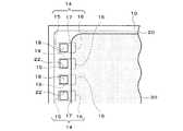
以下、本発明の実施の形態について図面を参照して説明する。ただし、本発明は、以下の実施の形態に限定されるものではない。なお、図1は、本発明の実施の形態に係る半導体装置の断面図である。また、図2は、本実施の形態に係る半導体装置から、配線40、レジスト層50、被覆層60及び外部端子46を取り除いたものを、平面図で示したものである。
【0006】
半導体装置は、半導体基板10を有する。半導体基板10は、半導体チップであってもよいし、半導体ウエハであってもよい。半導体基板10には、1つ又は複数の集積回路12が形成されている。半導体チップには1つの集積回路12が形成され、半導体ウエハには複数の集積回路12が形成されている。半導体基板10は、複数の電極(例えばパッド)14を有する。電極14は、例えばAlで形成されてもよい。電極14は、集積回路12に電気的に接続されていてもよい。あるいは、集積回路12に電気的に接続されていない電極を、電極14としてもよい。電極14は、半導体基板10の周縁側の第1の端部15と、半導体基板10の中央側の第2の端部16とを有する。また、電極14は、第1の端部15と第2の端部16とによって挟まれた中間部17を含む。
【0007】
半導体基板10の電極14が形成された面には、パッシベーション膜20が形成されていてもよい。この場合、パッシベーション膜20は、電極14の一部を露出する開口22を有する。開口22が電極14の中間部17に配置されるように、パッシベーション膜20が形成されてもよい。また、開口22の中心が電極14の中心から半導体基板10の外方向へずれた位置に配置されるように、パッシベーション膜20が形成されてもよい。パッシベーション膜20は、SiN、SiO2、ポリイミド樹脂等によって形成されてもよい。
【0008】
半導体装置は、樹脂層30を有する。樹脂層30は、半導体基板10の電極14が形成された面に設けられてなる。樹脂層30は、半導体基板10の周縁から電極14の第1の端部15までの領域を避けて、電極14の第2の端部16とオーバーラップするように形成されてなる。樹脂層30は、電極14の中間部17の中央部を避けて形成されてもよい。樹脂層30は、電極14の中間部17における端部19とオーバーラップするように形成されてもよい。あるいは、樹脂層30は、端部19とオーバーラップしないように形成されてもよい。半導体基板10がパッシベーション膜20を有する場合、樹脂層30は、パッシベーション膜20上に形成されてなる。そして、樹脂層30は、パッシベーション膜20を介して、第2の端部16とオーバーラップする。このとき、樹脂層30は、電極14のパッシベーション膜20の開口22からの露出部18を避けて形成されてもよい。樹脂層30は、応力緩和機能を有していてもよい。樹脂層30は、ポリイミド樹脂、シリコーン変性ポリイミド樹脂、エポキシ樹脂、シリコーン変性エポキシ樹脂、ベンゾシクロブテン(BCB;Benzocyclobutene)、ポリベンゾオキサゾール(PBO;Polybenzoxazole)等の樹脂で形成することができる。樹脂層30は、半導体基板10と外部端子46との間に形成されてもよい。
【0009】
上述したように、本実施の形態に係る半導体装置の樹脂層30は、電極14の一部とオーバーラップするように設けられる。そのため、電極14における電気的な導通を図る部分(例えば露出部18)に近接する位置まで樹脂層30を形成することが可能となる。そのため、樹脂層30の平面面積を大きくとることができ、配線の引き回しの自由度を高めることができる。また、樹脂層30は電極14よりも外側の領域(詳しくは、半導体基板10の周縁から電極14の第1の端部15までの領域)には形成されない。そのため、樹脂が収縮した場合でも、樹脂層30が、電極14における電気的な導通を図る部分上に配置されることを防止することができ、電気的な接続信頼性を高めることができる。すなわち、本発明によって実装性及び電気的な接続信頼性の高い半導体装置を提供することができる。なお、パッシベーション膜20が、開口22の中心が電極14の中心から半導体基板10の外方向へずれた位置に配置されるように形成されている場合、樹脂層30の平面面積をさらに大きくすることができるため、さらに実装性に優れた半導体装置を提供することができる。
【0010】
半導体装置は、1つ又は複数の配線40を有する。各配線40は、1層又は複数層で形成されてもよい。配線40は、電極14における開口22からの露出部18の全てを覆っていてもよい。配線40は、電極14から樹脂層30の上面(パッシベーション膜20側とは反対側の面)に至るように形成されてなる。図1に示すように、配線40は、樹脂層30の側面を通るように形成されてもよい。
【0011】
半導体装置は、複数の外部端子46を有してもよい。外部端子46は、配線40に電気的に接続されている。外部端子46は、配線40のランド48の上に形成されてもよい。外部端子46は、導電性を有する金属(例えば合金)であって、溶融させて電気的な接続を図るもの(例えばハンダ)である。外部端子46は、軟ろう(soft solder)又は硬ろう(hard solder)のいずれで形成されてもよい。外部端子46は、球状をなしてもよく、例えばハンダボールであってもよい。
【0012】
半導体装置は、レジスト層50を有してもよい。レジスト層50は、配線40の少なくとも一部を覆っている。配線40の、外部端子46が設けられた部分を除いた部分を全てレジスト層50で覆うことで、配線40の酸化、腐食を防止し、電気的な不良を防止することができる。レジスト層50は、配線40のランド48の少なくとも中央部を除いて形成されてもよい。レジスト層50は、ランド48の周縁部を覆ってもよい。
【0013】
半導体装置は、被覆層60を有してもよい。被覆層60はレジスト層50上に形成されてもよい。被覆層60は、外部端子46の根本部(下端部)を覆うように形成してもよい。被覆層60は、レジスト層50上に形成された部分と、この部分から立ち上がって外部端子46の根本部を覆う部分とを有してもよい(図1参照)。被覆層60によって外部端子46の少なくとも根元部を補強することができる。そのため、半導体装置が回路基板に実装された後に、被覆層60によって外部端子46への応力の集中を分散させることができる。
【0014】
半導体基板10が半導体チップである場合、半導体装置は、そのパッケージサイズが半導体チップにほぼ等しくなり、CSPに分類することができる。あるいは、応力緩和機能を備えるフリップチップであるということもできる。
【0015】
本実施の形態に係る半導体装置は、以上のように形成されてなり、以下その製造方法を説明する。本実施の形態に係る半導体装置の製造方法は、電極14を有し集積回路12が形成されてなる半導体基板10に、樹脂層30を形成することを含む。樹脂層30は、半導体基板10の電極14が形成された面に形成する。なお、電極14は、半導体基板10の周縁側の第1の端部15と、半導体基板10の中央側の第2の端部16とを有する。また、電極14は、第1の端部15と第2の端部16とによって挟まれた中間部17を有してもよい。半導体基板10には、パッシベーション膜20が形成されていてもよく、このとき、樹脂層をパッシベーション膜20上に形成してもよい。なお、パッシベーション膜20は、先に説明した内容を適用してもよい。半導体基板10は、半導体チップであってもよく、半導体ウエハであってもよい。半導体ウエハを半導体基板10とした場合、複数の半導体装置を一括で製造することが可能なため、効率よく半導体装置を製造することができる。
【0016】
本実施の形態では、樹脂層30を、半導体基板10の周縁から電極14の第1の端部15までの領域を避けて、電極14の第2の端部16とオーバーラップするように形成する。樹脂層30を、電極14の中間部17の中央部を避けて形成してもよい。樹脂層30を、電極14の中間部17における端部19とオーバーラップするように形成してもよい。あるいは、樹脂層30を、端部19とオーバーラップしないように形成してもよい。半導体基板10がパッシベーション膜20を有する場合、樹脂層30を、電極14の露出部18を避けて形成してもよい。例えば、予め定めた領域にのみ樹脂を形成することで、樹脂層30を形成してもよい。また、半導体基板10の電極が形成された面の全面に樹脂層を形成し、その後不要な部分を除去することで樹脂層30を形成してもよい。このとき、例えばフォトリソグラフィ技術や、エッチングによって、樹脂層の一部を除去してもよい。
【0017】
次に、配線40を形成する。配線40は、電極14から樹脂層30上に至るように形成する。既に公知となっているいずれの方法によって、配線40を形成してもよい。例えば、スパッタリングを利用して配線40を形成してもよいし、無電解メッキで配線40を形成するアディティブ法を適用してもよい。あるいは、インクジェット方式で導電ペーストを塗布することで、配線40を形成してもよい。
【0018】
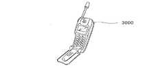
最後に、外部端子46、レジスト層50、被覆層60等を形成し、半導体基板10が半導体ウエハである場合、個々の半導体装置1に切り出す工程を経て、本実施の形態に係る半導体装置1を製造することができる。なお、図3には、本実施の形態に係る半導体装置1が実装された回路基板1000を示す。また、半導体装置1を有する電子機器として、図4にはノート型パーソナルコンピュータ2000を、図5には携帯電話3000を、それぞれ示す。
【0019】
なお、本発明は、上述した実施の形態に限定されるものではなく、種々の変形が可能である。例えば、本発明は、実施の形態で説明した構成と実質的に同一の構成(例えば、機能、方法及び結果が同一の構成、あるいは目的及び効果が同一の構成)を含む。また、本発明は、実施の形態で説明した構成の本質的でない部分を置き換えた構成を含む。また、本発明は、実施の形態で説明した構成と同一の作用効果を奏する構成又は同一の目的を達成することができる構成を含む。また、本発明は、実施の形態で説明した構成に公知技術を付加した構成を含む。
【図面の簡単な説明】
【図1】 図1は、本発明を適用した実施の形態に係る半導体装置を示す図である。
【図2】 図2は、本発明を適用した実施の形態に係る半導体装置を示す図である。
【図3】 図3は、本発明を適用した実施の形態に係る半導体装置が実装された回路基板を示す図である。
【図4】 図4は、本発明を適用した実施の形態に係る半導体装置を有する電子機器を示す図である。
【図5】 図5は、本発明を適用した実施の形態に係る半導体装置を有する電子機器を示す図である。
【符号の説明】
10 半導体基板、 12 集積回路、 14 電極、 15 第1の端部、 16 第2の端部、 20 パッシベーション膜、 30 樹脂層、 40配線[0001]
BACKGROUND OF THE INVENTION
The present invention relates to a semiconductor device, a manufacturing method thereof, a circuit board, and an electronic device.
[0002]
BACKGROUND OF THE INVENTION
The spread rate of CSP (chip scale / size package) is increasing as a package of a semiconductor device. In addition, a technique for manufacturing a package at a wafer level (wafer level package) has been developed. A package (for example, wafer level CSP) manufactured by this method has a semiconductor chip size as an external dimension. Therefore, it is important to improve mountability by increasing the degree of freedom of wiring. In addition, the structure is different from that of the conventional package, but the same or higher reliability as that of the conventional package is required.
[0003]
An object of the present invention is to provide a highly mountable and reliable semiconductor device, a manufacturing method thereof, a circuit board, and an electronic apparatus.
[0004]
[Means for Solving the Problems]
(1) In a semiconductor device according to the present invention, an integrated circuit is formed, a semiconductor substrate having electrodes,
A resin layer provided on a surface of the semiconductor substrate on which the electrode is formed;
Wiring formed on the resin layer from the electrodes;
Have
The electrode has a first end on the peripheral side of the semiconductor substrate, and a second end on the center side of the semiconductor substrate,
The resin layer is formed so as to overlap the second end portion, avoiding a region from the periphery of the semiconductor substrate to the first end portion of the electrode. According to the present invention, the resin layer is provided so as to overlap with a part of the electrode. Therefore, the resin layer can be formed up to a position close to the portion where electrical conduction is made in the electrode, and the planar area of the resin layer can be increased. Further, the resin layer is not formed in a region outside the electrode. Therefore, even when the resin layer is formed at a position close to the portion where electrical conduction is made in the electrode, the resin layer is prevented from being placed on the portion where electrical conduction is made in the electrode due to the shrinkage of the resin. Can do. Therefore, a semiconductor device with high mountability and high electrical connection reliability can be provided.
(2) In this semiconductor device,
A passivation film having an opening exposing a part of the electrode is formed on the surface of the semiconductor substrate on which the electrode is formed,
The resin layer may be formed on the passivation film.
(3) In this semiconductor device,
The resin layer may be formed to avoid an exposed portion from the opening of the electrode. According to this, the resin layer is not disposed on the portion of the electrode where electrical conduction is intended. Therefore, a semiconductor device with high electrical connection reliability can be provided.
(4) In this semiconductor device,
The center of the opening may be formed at a position shifted from the center of the electrode toward the outside of the semiconductor substrate. According to this, since the formation region of the resin layer can be further widened, it is possible to provide a semiconductor device having a higher degree of freedom in wiring.
(5) The above-described semiconductor device is mounted on the circuit board according to the present invention.
(6) An electronic apparatus according to the present invention includes the semiconductor device.
(7) A method for manufacturing a semiconductor device according to the present invention includes forming a resin layer on a surface of asemiconductor substrate having an electrode and an integrated circuit, on which the electrode is provided, and
Forming a wiring on the resin layer from the electrode;
Including
The electrode has a first end on the peripheral side of the semiconductor substrate, and a second end on the center side of the semiconductor substrate,
The resin layer is formed so as to overlap the second end portion, avoiding a region from the periphery of the semiconductor substrate to the first end portion of the electrode. According to the present invention, the resin layer is formed so as to overlap a part of the electrode. Therefore, the resin layer can be formed up to a position close to the portion where electrical conduction is made in the electrode, and the planar area of the resin layer can be increased. Further, the resin layer is not formed in a region outside the electrode. Therefore, even when the resin layer is formed at a position close to the portion where electrical conduction is made in the electrode, the resin layer is prevented from being placed on the portion where electrical conduction is made in the electrode due to the shrinkage of the resin. Can do. Therefore, a semiconductor device with high mountability and high electrical connection reliability can be manufactured.
(8) In this method of manufacturing a semiconductor device,
A passivation film having an opening exposing a part of the electrode is formed on the surface of the semiconductor substrate on which the electrode is formed,
The resin layer may be formed on the passivation film.
(9) In this method of manufacturing a semiconductor device,
The resin layer may be formed avoiding an exposed portion from the opening of the electrode. According to this, the resin layer is not disposed on the portion of the electrode where electrical conduction is intended. Therefore, a semiconductor device with high electrical connection reliability can be manufactured.
(10) In this method of manufacturing a semiconductor device,
The center of the opening may be formed at a position shifted from the center of the electrode toward the outside of the semiconductor substrate. According to this, since the formation region of the resin layer can be further widened, a semiconductor device having a higher degree of freedom in wiring routing can be manufactured.
[0005]
DETAILED DESCRIPTION OF THE INVENTION
Hereinafter, embodiments of the present invention will be described with reference to the drawings. However, the present invention is not limited to the following embodiments. FIG. 1 is a cross-sectional view of a semiconductor device according to an embodiment of the present invention. FIG. 2 is a plan view of the semiconductor device according to the present embodiment in which the
[0006]
The semiconductor device has a
[0007]
A
[0008]
The semiconductor device has a
[0009]
As described above, the
[0010]
The semiconductor device has one or a plurality of
[0011]
The semiconductor device may have a plurality of
[0012]
The semiconductor device may have a resist
[0013]
The semiconductor device may have a
[0014]
When the
[0015]
The semiconductor device according to the present embodiment is formed as described above, and the manufacturing method thereof will be described below. The method for manufacturing a semiconductor device according to the present embodiment includes forming a
[0016]
In the present embodiment, the
[0017]
Next, the
[0018]
Finally, when the
[0019]
In addition, this invention is not limited to embodiment mentioned above, A various deformation | transformation is possible. For example, the present invention includes configurations that are substantially the same as the configurations described in the embodiments (for example, configurations that have the same functions, methods, and results, or configurations that have the same objects and effects). In addition, the invention includes a configuration in which a non-essential part of the configuration described in the embodiment is replaced. In addition, the present invention includes a configuration that exhibits the same operational effects as the configuration described in the embodiment or a configuration that can achieve the same object. Further, the invention includes a configuration in which a known technique is added to the configuration described in the embodiment.
[Brief description of the drawings]
FIG. 1 is a diagram illustrating a semiconductor device according to an embodiment to which the present invention is applied.
FIG. 2 is a diagram illustrating a semiconductor device according to an embodiment to which the present invention is applied.
FIG. 3 is a diagram showing a circuit board on which a semiconductor device according to an embodiment to which the present invention is applied is mounted.
FIG. 4 is a diagram showing an electronic apparatus having a semiconductor device according to an embodiment to which the invention is applied.
FIG. 5 is a diagram illustrating an electronic apparatus including the semiconductor device according to the embodiment to which the invention is applied.
[Explanation of symbols]
DESCRIPTION OF
Claims (6)
Translated fromJapanese前記半導体基板の前記電極が形成された面に設けられた樹脂層と、
前記電極から前記樹脂層上に形成された配線と、
を有し、
前記電極は、前記半導体基板の周縁側の第1の端部と、前記半導体基板の中央側の第2の端部と、を有し、
前記半導体基板の前記電極が形成された面には、前記電極の一部を露出する開口を有するパッシベーション膜が形成されてなり、
前記樹脂層は、前記パッシベーション膜上に、前記半導体基板の周縁から前記電極の前記第1の端部までの領域を避けて、前記第2の端部とオーバーラップするように形成されてなり、
前記パッシベーション膜の前記開口の中心は、前記電極の中心から前記半導体基板の外方向へずれた位置に配置されてなる半導体装置。An integrated circuit is formed, and a semiconductor substrate having electrodes;
A resin layer provided on a surface of the semiconductor substrate on which the electrode is formed;
Wiring formed on the resin layer from the electrodes;
Have
The electrode has a first end on the peripheral side of the semiconductor substrate, and a second end on the center side of the semiconductor substrate,
A passivation film having an opening exposing a part of the electrode is formed on the surface of the semiconductor substrate on which the electrode is formed,
The resin layer is formed on the passivation film so as to avoid the region from the periphery of the semiconductor substrate to the first end of the electrode, and to overlap the second end,
A semiconductor device in which a center of the opening of the passivation film is arranged at a position shifted outward from the center of the electrode.
前記樹脂層は、前記電極の前記開口からの露出部を避けて形成されてなる半導体装置。The semiconductor device according to claim 1,
The said resin layer is a semiconductor device formed by avoiding the exposed part from the said opening of the said electrode.
前記電極から前記樹脂層上に配線を形成すること、
を含み、
前記電極は、前記半導体基板の周縁側の第1の端部と、前記半導体基板の中央側の第2の端部と、を有し、
前記半導体基板の前記電極が形成された面には、前記電極の一部を露出する開口を有するパッシベーション膜が形成されてなり、
前記開口の中心は、前記電極の中心から前記半導体基板の外方向へずれた位置に配置されてなり、
前記樹脂層を、前記パッシベーション膜上に、前記半導体基板の周縁から前記電極の前記第1の端部までの領域を避けて、前記第2の端部とオーバーラップするように形成する半導体装置の製造方法。Forming a resin layer on a surface of the semiconductor device having an electrode and an integrated circuit formed with the electrode; and
Forming a wiring on the resin layer from the electrode;
Including
The electrode has a first end on the peripheral side of the semiconductor substrate, and a second end on the center side of the semiconductor substrate,
A passivation film having an opening exposing a part of the electrode is formed on the surface of the semiconductor substrate on which the electrode is formed,
The center of the opening is arranged at a position shifted from the center of the electrode to the outside of the semiconductor substrate,
In the semiconductor device, the resin layer is formed on the passivation film so as to avoid the region from the periphery of the semiconductor substrate to the first end of the electrode and to overlap the second end. Production method.
前記樹脂層を、前記電極の前記開口からの露出部を避けて形成する半導体装置の製造方法。In the manufacturing method of the semiconductor device according to claim 5,
A method of manufacturing a semiconductor device, wherein the resin layer is formed so as to avoid an exposed portion from the opening of the electrode.
Priority Applications (2)
| Application Number | Priority Date | Filing Date | Title |
|---|---|---|---|
| JP2003073925AJP3726906B2 (en) | 2003-03-18 | 2003-03-18 | Semiconductor device and manufacturing method thereof, circuit board, and electronic apparatus |
| US10/802,668US7057282B2 (en) | 2003-03-18 | 2004-03-17 | Semiconductor device and method for manufacturing the same, circuit board and electronic equipment |
Applications Claiming Priority (1)
| Application Number | Priority Date | Filing Date | Title |
|---|---|---|---|
| JP2003073925AJP3726906B2 (en) | 2003-03-18 | 2003-03-18 | Semiconductor device and manufacturing method thereof, circuit board, and electronic apparatus |
Publications (3)
| Publication Number | Publication Date |
|---|---|
| JP2004281896A JP2004281896A (en) | 2004-10-07 |
| JP2004281896A5 JP2004281896A5 (en) | 2005-08-25 |
| JP3726906B2true JP3726906B2 (en) | 2005-12-14 |
Family
ID=33289703
Family Applications (1)
| Application Number | Title | Priority Date | Filing Date |
|---|---|---|---|
| JP2003073925AExpired - Fee RelatedJP3726906B2 (en) | 2003-03-18 | 2003-03-18 | Semiconductor device and manufacturing method thereof, circuit board, and electronic apparatus |
Country Status (2)
| Country | Link |
|---|---|
| US (1) | US7057282B2 (en) |
| JP (1) | JP3726906B2 (en) |
Families Citing this family (3)
| Publication number | Priority date | Publication date | Assignee | Title |
|---|---|---|---|---|
| JP2007115957A (en) | 2005-10-21 | 2007-05-10 | Seiko Epson Corp | Semiconductor device and manufacturing method thereof |
| JP2007115958A (en)* | 2005-10-21 | 2007-05-10 | Seiko Epson Corp | Semiconductor device |
| US10483132B2 (en) | 2012-12-28 | 2019-11-19 | Taiwan Semiconductor Manufacturing Company, Ltd. | Post-passivation interconnect structure and method of forming the same |
Family Cites Families (11)
| Publication number | Priority date | Publication date | Assignee | Title |
|---|---|---|---|---|
| JP2730492B2 (en) | 1994-10-25 | 1998-03-25 | 日本電気株式会社 | Semiconductor device |
| JP3618212B2 (en) | 1998-01-08 | 2005-02-09 | 松下電器産業株式会社 | Semiconductor device and manufacturing method thereof |
| JPH11224885A (en) | 1998-02-06 | 1999-08-17 | Matsushita Electron Corp | Semiconductor device |
| US6396145B1 (en)* | 1998-06-12 | 2002-05-28 | Hitachi, Ltd. | Semiconductor device and method for manufacturing the same technical field |
| US6940160B1 (en) | 1999-03-16 | 2005-09-06 | Seiko Epson Corporation | Semiconductor device and method of manufacture thereof, circuit board, and electronic instrument |
| JP3729680B2 (en) | 1999-06-03 | 2005-12-21 | 株式会社ルネサステクノロジ | Semiconductor device manufacturing method and semiconductor device |
| JP4015787B2 (en) | 1999-09-03 | 2007-11-28 | 松下電器産業株式会社 | Manufacturing method of semiconductor device |
| JP3452043B2 (en) | 1999-10-29 | 2003-09-29 | 株式会社日立製作所 | Semiconductor device and manufacturing method thereof |
| JP3399456B2 (en) | 1999-10-29 | 2003-04-21 | 株式会社日立製作所 | Semiconductor device and manufacturing method thereof |
| TW515064B (en) | 2000-03-23 | 2002-12-21 | Seiko Epson Corp | Semiconductor device and its manufacturing method, circuit board and electronic machine |
| JP2004104102A (en)* | 2002-08-21 | 2004-04-02 | Seiko Epson Corp | Semiconductor device and its manufacturing method, circuit board, and electronic equipment |
- 2003
- 2003-03-18JPJP2003073925Apatent/JP3726906B2/ennot_activeExpired - Fee Related
- 2004
- 2004-03-17USUS10/802,668patent/US7057282B2/ennot_activeExpired - Lifetime
Also Published As
| Publication number | Publication date |
|---|---|
| US20040245629A1 (en) | 2004-12-09 |
| US7057282B2 (en) | 2006-06-06 |
| JP2004281896A (en) | 2004-10-07 |
Similar Documents
| Publication | Publication Date | Title |
|---|---|---|
| US6528881B1 (en) | Semiconductor device utilizing a side wall to prevent deterioration between electrode pad and barrier layer | |
| JP2001110831A (en) | External connection projection and method of forming the same, semiconductor chip, circuit board, and electronic device | |
| JP2004158827A (en) | Semiconductor wafer, semiconductor device and its manufacturing method, circuit board, and electronic equipment | |
| JP3678239B2 (en) | Semiconductor device and manufacturing method thereof, circuit board, and electronic apparatus | |
| JP3804797B2 (en) | Semiconductor device and manufacturing method thereof | |
| JP2004281898A (en) | Semiconductor device and its manufacturing method, circuit board, and electronic equipment | |
| JP2004327480A (en) | Semiconductor device and its manufacturing method, electronic device and its manufacturing method, and electronic equipment | |
| JP3726906B2 (en) | Semiconductor device and manufacturing method thereof, circuit board, and electronic apparatus | |
| JP2003282790A (en) | Semiconductor device and its manufacturing method, circuit board, and electronic equipment | |
| JP4061506B2 (en) | Manufacturing method of semiconductor device | |
| JP2004260074A (en) | Semiconductor device, method of manufacturing semiconductor device and method of mounting the same, circuit board, and electronic device | |
| JP4145902B2 (en) | Semiconductor device and manufacturing method thereof | |
| JP2006287094A (en) | Semiconductor device and manufacturing method thereof | |
| JP2004172163A (en) | Semiconductor device and manufacturing method thereof | |
| JP4352263B2 (en) | Semiconductor device and manufacturing method thereof, circuit board, and electronic apparatus | |
| JP3928729B2 (en) | Semiconductor device | |
| JP3666495B2 (en) | Semiconductor device and manufacturing method thereof, circuit board, and electronic apparatus | |
| JP4058630B2 (en) | Semiconductor device and manufacturing method thereof, circuit board, and electronic apparatus | |
| JP2004281897A (en) | Semiconductor device and its manufacturing method, circuit board, and electronic equipment | |
| JP2005026299A (en) | Semiconductor device and manufacturing method thereof, circuit board, and electronic apparatus | |
| JP4240226B2 (en) | Semiconductor device and manufacturing method thereof, circuit board, and electronic apparatus | |
| JP4038691B2 (en) | Semiconductor device and manufacturing method thereof, circuit board, and electronic apparatus | |
| JP4016276B2 (en) | Semiconductor device and manufacturing method thereof, circuit board, and electronic apparatus | |
| JP2007142481A (en) | Semiconductor device, circuit board and electronic equipment | |
| JP4359785B2 (en) | Semiconductor device |
Legal Events
| Date | Code | Title | Description |
|---|---|---|---|
| A521 | Written amendment | Free format text:JAPANESE INTERMEDIATE CODE: A523 Effective date:20050215 | |
| A621 | Written request for application examination | Free format text:JAPANESE INTERMEDIATE CODE: A621 Effective date:20050215 | |
| A871 | Explanation of circumstances concerning accelerated examination | Free format text:JAPANESE INTERMEDIATE CODE: A871 Effective date:20050215 | |
| A975 | Report on accelerated examination | Free format text:JAPANESE INTERMEDIATE CODE: A971005 Effective date:20050311 | |
| A977 | Report on retrieval | Free format text:JAPANESE INTERMEDIATE CODE: A971007 Effective date:20050518 | |
| A131 | Notification of reasons for refusal | Free format text:JAPANESE INTERMEDIATE CODE: A131 Effective date:20050614 | |
| A521 | Written amendment | Free format text:JAPANESE INTERMEDIATE CODE: A523 Effective date:20050811 | |
| TRDD | Decision of grant or rejection written | ||
| A01 | Written decision to grant a patent or to grant a registration (utility model) | Free format text:JAPANESE INTERMEDIATE CODE: A01 Effective date:20050907 | |
| A61 | First payment of annual fees (during grant procedure) | Free format text:JAPANESE INTERMEDIATE CODE: A61 Effective date:20050920 | |
| R150 | Certificate of patent or registration of utility model | Free format text:JAPANESE INTERMEDIATE CODE: R150 | |
| FPAY | Renewal fee payment (event date is renewal date of database) | Free format text:PAYMENT UNTIL: 20091007 Year of fee payment:4 | |
| FPAY | Renewal fee payment (event date is renewal date of database) | Free format text:PAYMENT UNTIL: 20101007 Year of fee payment:5 | |
| FPAY | Renewal fee payment (event date is renewal date of database) | Free format text:PAYMENT UNTIL: 20101007 Year of fee payment:5 | |
| FPAY | Renewal fee payment (event date is renewal date of database) | Free format text:PAYMENT UNTIL: 20111007 Year of fee payment:6 | |
| FPAY | Renewal fee payment (event date is renewal date of database) | Free format text:PAYMENT UNTIL: 20121007 Year of fee payment:7 | |
| FPAY | Renewal fee payment (event date is renewal date of database) | Free format text:PAYMENT UNTIL: 20121007 Year of fee payment:7 | |
| FPAY | Renewal fee payment (event date is renewal date of database) | Free format text:PAYMENT UNTIL: 20131007 Year of fee payment:8 | |
| S531 | Written request for registration of change of domicile | Free format text:JAPANESE INTERMEDIATE CODE: R313531 | |
| R350 | Written notification of registration of transfer | Free format text:JAPANESE INTERMEDIATE CODE: R350 | |
| LAPS | Cancellation because of no payment of annual fees |