JP3726898B2 - Data transfer control device, electronic device, and data transfer control method - Google Patents
Data transfer control device, electronic device, and data transfer control methodDownload PDFInfo
- Publication number
- JP3726898B2 JP3726898B2JP2002126880AJP2002126880AJP3726898B2JP 3726898 B2JP3726898 B2JP 3726898B2JP 2002126880 AJP2002126880 AJP 2002126880AJP 2002126880 AJP2002126880 AJP 2002126880AJP 3726898 B2JP3726898 B2JP 3726898B2
- Authority
- JP
- Japan
- Prior art keywords
- transfer
- data
- controller
- sof
- packet
- Prior art date
- Legal status (The legal status is an assumption and is not a legal conclusion. Google has not performed a legal analysis and makes no representation as to the accuracy of the status listed.)
- Expired - Fee Related
Links
Images


Classifications
- G—PHYSICS
- G06—COMPUTING OR CALCULATING; COUNTING
- G06F—ELECTRIC DIGITAL DATA PROCESSING
- G06F13/00—Interconnection of, or transfer of information or other signals between, memories, input/output devices or central processing units
- G06F13/38—Information transfer, e.g. on bus
- G06F13/42—Bus transfer protocol, e.g. handshake; Synchronisation
- G06F13/4282—Bus transfer protocol, e.g. handshake; Synchronisation on a serial bus, e.g. I2C bus, SPI bus
- G06F13/4286—Bus transfer protocol, e.g. handshake; Synchronisation on a serial bus, e.g. I2C bus, SPI bus using a handshaking protocol, e.g. RS232C link
Landscapes
- Engineering & Computer Science (AREA)
- Theoretical Computer Science (AREA)
- Physics & Mathematics (AREA)
- General Engineering & Computer Science (AREA)
- General Physics & Mathematics (AREA)
- Information Transfer Systems (AREA)
- Bus Control (AREA)
- Small-Scale Networks (AREA)
- Communication Control (AREA)
Description
Translated fromJapanese【0001】
【発明の属する技術分野】
本発明は、データ転送制御装置、電子機器及びデータ転送制御方法に関する。
【0002】
【背景技術及び発明が解決しようとする課題】
USB(Universal Serial Bus)2.0の市場が順調に拡大しているなか、USB Implementers Forum(USB−IF)によって、USB On−The−Go(OTG)と呼ばれるインターフェース規格が策定された。USB2.0を拡張する形で策定されたOTG規格(OTG1.0)は、USBインターフェースの新たな付加価値を生む可能性を秘めており、その特質を生かしたアプリケーションの登場が待たれている。
【0003】
このOTGによれば、これまでUSBを介してホスト(パーソナルコンピュータ等)に接続されていたペリフェラル(周辺機器)に、ホスト機能を持たせることができる。これにより、ペリフェラル同士をUSBで接続してデータを転送することが可能になり、例えばデジタルカメラとプリンタとをダイレクトに接続して、デジタルカメラの画像を印刷することが可能になる。また、デジタルカメラやデジタルビデオカメラをストレージ装置に接続して、データを保存することが可能になる。
【0004】
しかしながら、OTGによりホスト機能を持たせるペリフェラルには、低性能のCPU(処理部)が組み込まれているのが一般的である。従って、ホスト機能の追加により、ペリフェラルが有するCPU(ファームウェア)の処理負荷が重くなったり、処理が複雑化すると、他の処理に支障が生じたり、機器の設計期間が長期化するなどの問題が生じる。
【0005】
また、USB1.1、USB2.0、OTGなどのUSB規格では、アイソクロナス転送、バルク転送、コントロール転送、インタラプト転送という4種類の転送タイプが定義されている。USBのホストは、これらの各転送タイプのパケットの転送順序を管理し、フレームの残り時間を考慮しながら、各転送タイプのパケットを転送する。このために、USBではホストがフレーム管理を行い、FS(Full Speed)、LS(Low Speed)では1ms毎に、HS(High Speed)では125μs毎に、SOF(Start Of Frame)パケットをホストがペリフェラル(デバイス)に転送する。
【0006】
しかしながら、バルク転送やコントロール転送などの非周期転送では、このようなSOFパケットの転送はバス帯域を狭める結果となり、転送効率が低下してしまうという課題があることが判明した。
【0007】
本発明は、以上のような技術的課題に鑑みてなされたものであり、その目的とするところは、非周期転送時の転送効率を向上できるデータ転送制御装置、電子機器及びデータ転送制御方法を提供することにある。
【0008】
【課題を解決するための手段】
本発明は、バスを介したデータ転送のためのデータ転送制御装置であって、転送データを記憶するパケットバッファのアクセス制御を行うバッファコントローラと、パケットバッファのデータの転送を制御する転送コントローラとを含み、前記転送コントローラが、第1のモードが設定された場合には、SOF(Start Of Frame)パケットをフレーム周期で転送しながらデータ転送を行い、第2のモードが設定され且つ非周期転送を行う場合には、SOFパケットの周期転送を無効にして、非周期データの転送を行うデータ転送制御装置に関係する。
【0009】
本発明では、第1のモードの設定時には、SOFパケットがフレーム周期で転送されながら、データ転送が行われる。これにより、例えばアイソクロナス転送等の周期転送を適正に行うことが可能になる。一方、第2のモードの設定時には、SOFパケットの転送が無効にされて、非周期データの転送が行われる。これにより、複数のフレームの境界をまたがったトランザクションの発生等が可能になり、例えばバルク転送、コントロール転送等の非周期転送の転送効率を向上できる。
【0010】
また本発明では、前記転送コントローラが、転送すべき非周期データが無い場合には、第2のモードが設定された場合にも、SOFパケットをフレーム周期で転送するようにしてもよい。
【0011】
このようにすれば、バスに接続される他の機器が不適切なステートに移行してしまう事態等を防止できる。なお、転送すべき非周期データが有るか無いかは、例えば、転送開始指示信号や、パケットバッファのフル、エンプティ信号等により判断できる。
【0012】
また本発明では、ホストの役割として動作するホスト動作のステートと、ペリフェラルの役割として動作するペリフェラル動作のステートを含む複数のステートの制御を行うステートコントローラを含み、前記パケットバッファには、各エンドポイントとの間で転送されるデータが各パイプ領域に記憶される複数のパイプ領域が確保され、前記転送コントローラが、ホスト動作時において、ホストとしてのデータ転送を行うホストコントローラと、ペリフェラル動作時において、ペリフェラルとしてのデータ転送を行うペリフェラルコントローラとを含み、前記ホストコントローラが、エンドポイントに対するトランザクションを自動発生し、パイプ領域と、そのパイプ領域に対応するエンドポイントとの間で、データを自動転送するようにしてもよい。
【0013】
本発明によれば、例えば、ステートコントローラにより制御されるステートが、ホスト動作のステートになると、ホストコントローラにより、ホストの役割としてのデータ転送が行われる。また、ステートコントローラにより制御されるステートが、ペリフェラル動作のステートになると、ペリフェラルコントローラにより、ペリフェラルの役割としてのデータ転送が行われる。これにより、いわゆるデュアルロール・デバイス機能を実現できるようになる。
【0014】
そして本発明では、ホスト動作時において、パケットバッファに対して複数のパイプ領域が確保(allocate)され、確保されたパイプ領域とエンドポイントとの間で、データが自動転送される。これにより、デュアルロール・デバイス機能を実現できると共に、ホスト動作時における処理部の処理負荷を軽減できる。
【0015】
また本発明では、前記ホストコントローラが、第2のモードが設定された場合には、パイプ領域とそのパイプ領域に対応する非周期転送のエンドポイントとの間で、SOFパケットの周期転送を無効にしながら、非周期データを自動転送するようにしてもよい。
【0016】
このようにすれば、パイプ領域を用いて、非周期転送のエンドポイントとの間で、非周期データの自動転送が可能になり、データ転送を効率化できる。そして、この時に本発明では、SOFパケットの周期転送が無効になるため、データ転送を更に効率化できる。なお、SOFパケットの転送を無効にする場合(第2のモードに設定する場合)には、パケットバッファに確保されるパイプ領域に、周期転送(アイソクロナス転送等)以外の転送種別のエンドポイントを割り当てることが望ましい。
【0017】
また本発明では、前記ホストコントローラが、パイプ領域の自動転送指示信号が全て非アクティブの場合には、第2のモードが設定された場合にも、SOFパケットをフレーム周期で自動転送するようにしてもよい。
【0018】
このようにすれば、転送すべきデータが有るか無いかを、自動転送指示信号に基づいて判断できるため、判断処理を簡素化できる。そして、自動転送指示信号が全て非アクティブの場合(転送すべきデータが無い場合)に、SOFパケットを転送することで、バスに接続される他の機器が不適切なステートに移行してしまう事態等を防止できる。
【0019】
また本発明では、前記ホストコントローラが、フレーム周期毎にSOF転送開始トリガをアクティブにし、SOFパケットの転送が完了した場合に前記SOF転送開始トリガを非アクティブにするSOF転送開始トリガ生成回路と、パイプ領域の自動転送指示信号と、ステートコントローラからのステート情報信号と、第1又は第2のモードを指示する信号を受け、前記SOF転送開始トリガを無効にする信号を生成するSOF無効信号生成回路とを含んでもよい。
【0020】
このようにすれば、SOFパケットの転送を無効にする処理等を簡素な回路で実現できる。なお、例えば、ステート情報信号が示すステートがホスト動作であり、第2のモードが指示され、自動転送指示信号の少なくとも1つがアクティブの場合には、SOF転送開始トリガの無効信号をアクティブにして、SOF転送開始トリガの生成を無効にすることができる。一方、ステート情報信号が示すステートがホスト動作であり、第2のモードが指示された場合にも、自動転送指示信号が全て非アクティブの場合(転送すべきデータが無い場合)には、SOF転送開始トリガの無効信号を非アクティブにして、SOF転送開始トリガの生成が無効にされないようにすることができる。
【0021】
また本発明では、ペリフェラル動作時には、ホストとの間で転送されるデータが各エンドポイント領域に記憶される複数のエンドポイント領域が、パケットバッファに確保され、前記ペリフェラルコントローラが、エンドポイント領域とホストとの間でデータを転送するようにしてもよい。
【0022】
このようにすれば、パケットバッファのバッファ領域を、ホスト動作時にはパイプ領域として使用し、ペリフェラル動作時にはエンドポイント領域として使用できるようになる。これにより、パケットバッファのリソースの有効利用や、処理部の処理負荷の軽減化を図れる。
【0023】
また本発明では、前記非周期転送がUSB(Universal Serial Bus)規格のバルク転送又はコントロール転送であり、前記非周期データがバルクデータ又はコントロールデータであってもよい。
【0024】
また本発明では、USB(Universal Serial Bus)のOTG(On−The−Go)規格に準拠したデータ転送を行うようにしてもよい。
【0025】
また本発明は、上記のいずれかのデータ転送制御装置と、前記データ転送制御装置及びバスを介して転送されるデータの出力処理又は取り込み処理又は記憶処理を行う装置と、前記データ転送制御装置のデータ転送を制御する処理部とを含む電子機器に関係する。
【0026】
また本発明は、バスを介したデータ転送のためのデータ転送制御方法であって、転送データを記憶するパケットバッファのアクセス制御を行い、パケットバッファのデータの転送を制御すると共に、第1のモードが設定された場合には、SOF(Start Of Frame)パケットをフレーム周期で転送しながらデータ転送を行い、第2のモードが設定され且つ非周期転送を行う場合には、SOFパケットの周期転送を無効にして、非周期データの転送を行うデータ転送制御方法に関係する。
【0027】
【発明の実施の形態】
以下、本実施形態について説明する。
【0028】
なお、以下に説明する本実施形態は、特許請求の範囲に記載された本発明の内容を不当に限定するものではない。また本実施形態で説明される構成の全てが本発明の解決手段として必須であるとは限らない。
【0029】
1.OTG
まず、OTG(USB On−The−Go)について簡単に説明する。
【0030】
1.1 Aデバイス、Bデバイス
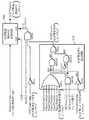
OTGでは、コネクタの規格として、図1(A)に示すようなMini-Aプラグ、Mini-Bプラグが定義されている。また、これらのMini-Aプラグ、Mini−Bプラグ(広義にはケーブルの第1、第2のプラグ)の両方を接続できるコネクタとして、Mini-ABレセプタクル(receptacle)が定義されている。
【0031】
そして例えば図1(B)のように、USBケーブルのMini-Aプラグに電子機器Pが接続され、Mini-Bプラグに電子機器Qが接続されると、電子機器PはAデバイスに設定され、電子機器QはBデバイスに設定される。一方、図1(C)に示すように、Mini-Bプラグ、Mini-Aプラグが電子機器P、Qに接続されると、電子機器P、Qは、各々、Bデバイス、Aデバイスに設定される。
【0032】
Mini-Aプラグ内ではIDピンがGNDに接続されており、Mini-Bプラグ内ではIDピンはフローティング状態になっている。電子機器は、内蔵するプルアップ抵抗回路を用いて、このIDピンの電圧レベルを検出することで、自身がMini-Aプラグに接続されたのか、或いはMini-Bプラグに接続されたのかを判断する。
【0033】
OTGでは、Aデバイス(マスター)が、電源(VBUS)を供給する側(供給元)になり、Bデバイス(スレイブ)が、電源の供給を受ける側(供給先)になる。また、Aデバイスは、デフォルトのステートがホストになり、Bデバイスは、デフォルトのステートがペリフェラル(周辺機器)になる。
【0034】
1.2 デュアルロール・デバイス
OTGでは、ホスト(簡易ホスト)としての役割とペリフェラルとしての役割の両方を持つことができるデュアルロール・デバイス(Dual-Role Device)が定義されている。
【0035】
デュアルロール・デバイスは、ホストにもペリフェラルにもなれる。そして、デュアルロール・デバイスに接続された相手が、従来のUSB規格におけるホストやペリフェラルである場合には、デュアルロール・デバイスの役割は一意に定まる。つまり、接続相手がホストであれば、デュアルロール・デバイスはペリフェラルになり、接続相手がペリフェラルであれば、デュアルロール・デバイスはホストになる。
【0036】
一方、接続相手がデュアルロール・デバイスである場合には、両方のデュアルロール・デバイスは、お互いにホストとペリフェラルの役割を交換できる。
【0037】
1.3 SRP、HNP
デュアルロール・デバイスは、図2(A)、(B)に示すようなセッション開始要求手順SRP(Session Request Protocol)やホスト交換手順HNP(Host Negotiation Protocol)の機能を持つ。
【0038】
ここでセッション開始要求手順SRPは、BデバイスがAデバイスに対して、VBUS(電源)の供給を要求するプロトコルである。
【0039】
バスを使用しない場合にOTGでは、AデバイスはVBUSの供給を停止できる。これにより、Aデバイスが例えば小型の携帯機器であった場合に、無駄な電力消費を防止できる。そして、AデバイスがVBUSの供給を停止した後に、BデバイスがVBUSを供給してもらいたい場合には、このSRPを使用して、Aデバイスに対してVBUSの供給の再開を要求する。
【0040】
図2(A)にSRPの流れを示す。図2(A)に示すように、Bデバイスは、データ・ライン・パルシングとVBUSパルシングを行うことで、Aデバイスに対してVBUSの供給を要求する。そして、AデバイスによるVBUSの供給の開始後に、Bデバイスのペリフェラル動作(peripheral operation)と、Aデバイスのホスト動作(host operation)が開始する。
【0041】
図1(A)〜図1(C)で説明したように、デュアルロール・デバイス同士の接続では、Mini-Aプラグが接続された側であるAデバイスがデフォルトのホストとなり、Mini-Bプラグが接続された側であるBデバイスがデフォルトのペリフェラルになる。そして、OTGでは、プラグの抜き差しを行わなくても、ホストとペリフェラルの役割を交換できる。HNPは、このホストとペリフェラルの役割を交換するためのプロトコルである。
【0042】
HNPの流れを図2(B)に示す。デフォルトのホストとして動作するAデバイスが、バスの使用を終了すると、バスがアイドル状態になる。その後に、Bデバイスがデータ信号線DP(D+)のプルアップ抵抗を無効にすると、AデバイスがDPのプルアップ抵抗を有効にする。これにより、Aデバイスの役割はホストからペリフェラルに変わり、ペリフェラルとしての動作を開始する。また、Bデバイスの役割はペリフェラルからホストに変わり、ホストとしての動作を開始する。
【0043】
その後、Bデバイスが、バスの使用を終了し、AデバイスがDPのプルアップ抵抗を無効にすると、Bデバイスが、DPのプルアップ抵抗を有効にする。これにより、Bデバイスの役割はホストからペリフェラルに戻り、ペリフェラルとしての動作を再開する。また、Aデバイスの役割はペリフェラルからホストに戻り、ホストとしての動作を再開する。
【0044】
以上に説明したOTGによれば、携帯電話やデジタルカメラなどの携帯機器をUSBのホストとして動作させ、携帯機器同士をピア・ツー・ピアで接続してデータ転送を行うことが可能になる。これにより、USBインターフェースに新たな付加価値を生むことができ、これまでには存在しなかったアプリケーションを創出できる。
【0045】
2.OHCI
さて、従来のUSBでは、ホストであるパーソナルコンピュータが有するデータ転送制御装置(ホストコントローラ)は、マイクロソフト社が提唱したOHCI(Open Host Controller Interface)や、UHCI(Universal Host Controller Interface)といった規格に準拠していた。また、使用されるOS(Operating System)も、マイクロソフト社のWindowsやアップル社のマッキントッシュのOSなどに限定されていた。
【0046】
しかしながら、OTGのターゲット・アプリケーションである小型携帯機器では、組み込まれるCPUのアーキテクチャや、使用されるOSは千差万別である。更に、パーソナルコンピュータのホストコントローラ向けに規格化されたOHCIやUHCIは、USBホストとしての機能をフルに実装することを前提としており、小型携帯機器への実装に最適であるとは言い難い。
【0047】
例えば、図3(A)に、OHCIで使用されるリスト構造のディスクリプタの一例を示す。
【0048】
図3(A)において、エンドポイントディスクリプタED1、ED2、ED3は、リンクポインタによりリンクされており、エンドポイント1、2、3とのコミュニケーションに必要な情報が含まれている。そして、これらのED1、ED2、ED3には、転送ディスクリプタTD11〜TD13、TD21、TD31〜TD32がリンクポインタにより更にリンクされている。そして、これらの転送ディスクリプタには、エンドポイント1、2、3との間で転送するパケットデータに必要な情報が含まれている。
【0049】
図3(A)のリスト構造のディスクリプタは、図3(B)のCPU610(広義には処理部)上で動作するファームウェア(ホストコントローラ・ドライバ)が作成し、システムメモリ620に書き込む。即ち、ファームウェアは、システム中のエンドポイントに対してエンドポイントディスクリプタを割り当て、エンドポイント情報等に基づいてエンドポイントディスクリプタ、転送ディスクリプタを作成する。そして、これらのディスクリプタをリンクポインタでリンクさせて、システムメモリ620に書き込む。
【0050】
データ転送制御装置600(ホストコントローラ)は、システムメモリ620に書き込まれたリスト構造のディスクリプタを読み出し、エンドポイントディスクリプタや転送ディスクリプタに記述される情報に基づいて、データ転送を実行する。
【0051】
具体的には、データ転送制御装置600(ホストコントローラ)は、ED1に基づいてエンドポイント1の情報を設定し、ED1にリンクされるTD11に基づいて、エンドポイント1との間でデータ転送を行う。次に、ED2に基づいてエンドポイント2の情報を設定し、ED2にリンクされるTD21に基づいて、エンドポイント2との間でデータ転送を行う。同様にして、データ転送制御装置600は、TD31、TD12、TD32、TD13に基づいてデータ転送を実行する。
【0052】
以上のように、OHCI準拠のデータ転送制御装置(ホストコントローラ)では、CPU上で動作するファームウェア(ホストコントローラ・ドライバ)が、図3(A)に示すような複雑な構造のディスクリプタを作成しなければならない。従って、CPUの処理負荷が非常に重い。
【0053】
この場合、従来のUSBでは、ホストの役割が割り当てられるのはパーソナルコンピュータだけであり、このパーソナルコンピュータは高性能のCPUを有している。従って、図3(A)に示すような複雑な構造のディスクリプタの作成も、余裕を持って行うことが可能であった。
【0054】
ところが、OTGのターゲットアプリケーションである小型携帯機器(デジタルカメラ、携帯電話等)に組み込まれるCPU(embedded CPU)は、パーソナルコンピュータのCPUに比べて、性能が格段に低いのが一般的である。従って、携帯機器にOTGのホスト動作を行わせると、携帯機器に組み込まれるCPUに過大な負荷がかかり、他の処理に支障が生じたり、データ転送のパフォーマンスが低下するなどの問題が生じる。
【0055】
3.構成例
図4に、以上のような問題を解決できる本実施形態のデータ転送制御装置の構成例を示す。なお、本実施形態のデータ転送制御装置は、図4の全ての回路ブロックを含む必要はなく、その一部の回路ブロックを省略してもよい。
【0056】
トランシーバ10(以下、適宜Xcvrと呼ぶ)は、差動データ信号DP、DMを用いてUSB(広義にはバス)のデータを送受信する回路であり、USBの物理層(PHY)回路12を含む。より具体的にはトランシーバ10は、DP、DMのラインステート(J、K、SE0等)の生成、シリアル/パラレル変換、パラレル/シリアル変換、ビットスタッフィング、ビットアンスタッフィング、NRZIデコード、NRZIエンコードなどを行う。なお、トランシーバ10をデータ転送制御装置の外部に設けるようにしてもよい。
【0057】
OTGコントローラ20(広義にはステートコントローラ。以下、適宜OTGCと呼ぶ)は、OTGのSRP機能やHNP機能(図2(A)、(B)参照)を実現するための種々の処理を行う。即ち、OTGコントローラ20は、ホストの役割として動作するホスト動作のステートや、ペリフェラルの役割として動作するペリフェラル動作のステートなどを含む複数のステートの制御を行う。
【0058】
より具体的には、OTG規格には、デュアルロール・デバイスのAデバイス時(図1(B)、(C)参照)のステート遷移やBデバイス時のステート遷移が定義されている。OTGコントローラ20は、これらのステート遷移を実現するためのステートマシーンを含む。また、OTGコントローラ20は、USBのデータラインステートや、VBUSレベルや、IDピンのステートを検出(監視)する回路を含む。そして、OTGコントローラ20が含むステートマシーンは、これらの検出情報に基づいて、そのステート(例えば、ホスト、ペリフェラル、サスペンド又はアイドルなどのステート)を変化させる。この場合のステートの遷移は、ハードウェア回路により実現してもよいし、ファームウェアがステートコマンドをレジスタに設定することで実現してもよい。そして、ステートが遷移すると、OTGコントローラ20は、遷移後のステートに基づいて、VBUSを制御したり、DP、DMのプルアップ抵抗/プルダウン抵抗の接続/非接続を制御する。また、ホストコントローラ50(以下、適宜HCと呼ぶ)、ペリフェラルコントローラ60(以下、適宜PCと呼ぶ)のイネーブル/ディスエーブルを制御する。
【0059】
HC/PC切り替え回路30(HC/PC・コモン回路)は、トランシーバ10と、ホストコントローラ50又はペリフェラルコントローラ60との間の接続の切り替え制御を行う。また、USBのデータ(DP、DM)のラインステートの生成の指示をトランシーバ10に対して行う。なお、接続の切り替え制御は、HC/PCセレクタ32により実現され、ラインステートの生成指示は、ラインステートコントローラ34により実現される。
【0060】
例えばOTGコントローラ20が、ホスト動作時(ホストステート時)にHCイネーブル信号をアクティブにすると、HC/PC切り替え回路30(HC/PCセレクタ32)は、トランシーバ10とホストコントローラ50を接続する。一方、OTGコントローラ20が、ペリフェラル動作時(ペリフェラルステート時)にPCイネーブル信号をアクティブにすると、HC/PC切り替え回路30は、トランシーバ10とペリフェラルコントローラ60を接続する。このようにすることで、ホストコントローラ50とペリフェラルコントローラ60とを排他的に動作させることが可能になる。
【0061】
転送コントローラ40は、USB(広義にはバス)を介したデータ転送を制御する回路であり、ホストコントローラ50(HC)とペリフェラルコントローラ60(PC)を含む。
【0062】
ここでホストコントローラ50は、ホスト動作時(OTGコントローラ20からのHCイネーブル信号のアクティブ時)に、ホストの役割としてのデータ転送制御を行う回路である。
【0063】
即ち、ホストコントローラ50は、ホスト動作時に、HC/PC切り替え回路30によりトランシーバ10に接続される。そしてホストコントローラ50は、レジスタ部70の転送条件レジスタ部72に設定された転送条件情報に基づいて、エンドポイントに対するトランザクションを自動発生する。そして、パケットバッファ100に確保(allocate)されたパイプ領域(PIPE0〜PIPEe。以下、適宜PIPEと呼ぶ)と、そのパイプ領域に対応するエンドポイントとの間で、データ(パケット)の自動転送(処理部が介在しないハードウェア回路によるデータ転送)を行う。
【0064】
より具体的にはホストコントローラ50は、複数のパイプ転送間の調停、フレームにおける時間管理、転送のスケジューリング、再送の管理などを行う。また、パイプ転送の転送条件情報(オペレーション情報)をレジスタ部70を介して管理する。また、トランザクションの管理を行ったり、パケットを生成/分解したり、サスペンド/レジューム/リセット状態生成の指示を行う。
【0065】
一方、ペリフェラルコントローラ60は、ペリフェラル動作時(OTGコントローラ20からのPCイネーブル信号のアクティブ時)に、ペリフェラルの役割としてのデータ転送制御を行う回路である。
【0066】
即ち、ペリフェラルコントローラ60は、ペリフェラル動作時に、HC/PC切り替え回路30によりトランシーバ10に接続される。そして、レジスタ部70の転送条件レジスタ部72に設定された転送条件情報に基づいて、パケットバッファ100に確保されたエンドポイント領域(EP0〜EPe。以下適宜EPと呼ぶ)とホストとの間でデータを転送する。
【0067】
より具体的には、ペリフェラルコントローラ60は、エンドポイント転送の転送条件情報(オペレーション情報)をレジスタ部70を介して管理する。また、トランザクションの管理を行ったり、パケットを生成/分解したり、リモート・ウェイクアップ信号生成の指示を行う。
【0068】
なお、エンドポイントは、ユニークなアドレスを割り当てることができる、ペリフェラル(デバイス)上のポイント(部分)である。ホストとペリフェラル(デバイス)との間でのデータ転送は、全て、このエンドポイントを経由して行われる。また、トランザクションは、トークンパケットと、オプショナルなデータパケットと、オプショナルなハンドシェークパケットにより構成される。
【0069】
レジスタ部70は、データ転送(パイプ転送、エンドポイント転送)制御、バッファアクセス制御、バッファ管理、割り込み制御、ブロック制御、或いはDMA制御などを行うための種々のレジスタを含む。なお、レジスタ部70が含むレジスタは、RAMなどのメモリにより実現してもよいし、Dフリップフロップなどにより実現してもよい。また、レジスタ部70のレジスタは、1つにまとめずに、各ブロック(HC、PC、OTGC、Xcvr等)に分散して配置してもよい。
【0070】
レジスタ部70は、転送条件レジスタ部72を含む。そして、この転送条件レジスタ部72は、ホスト動作時にパケットバッファ100に確保されるパイプ領域(PIPE0〜PIPEe)とエンドポイントとの間でのデータ転送の転送条件情報(転送制御情報)を記憶するレジスタを含む。これらの各転送条件レジスタは、パケットバッファ100の各パイプ領域に対応して設けられる。
【0071】
なお、ペリフェラル動作時には、パケットバッファ100にはエンドポイント領域(EP0〜EPe)が確保される。そして、転送条件レジスタ部72に設定された転送条件情報に基づいて、データ転送制御装置とホストとの間でのデータ転送が行われる。
【0072】
バッファコントローラ80(FIFOマネージャ)は、パケットバッファ100に対するアクセス(リード/ライト)制御や領域管理を行う。より具体的には、CPU(広義には処理部)、DMA(Direct Memory Access)、USBによるパケットバッファ100へのアクセス・アドレスを生成・管理する。また、CPU、DMA、USBによるパケットバッファ100へのアクセスの調停を行う。
【0073】
例えば、ホスト動作時には、バッファコントローラ80は、インターフェース回路110(CPU又はDMA)とパケットバッファ100の間のデータ転送経路と、パケットバッファ100とホストコントローラ50(USB)の間のデータ転送経路を設定(確立)する。
【0074】
一方、ペリフェラル動作時には、バッファコントローラ80は、インターフェース回路110(CPU又はDMA)とパケットバッファ100の間のデータ転送経路と、パケットバッファ100とペリフェラルコントローラ60(USB)の間のデータ転送経路を設定する。
【0075】
パケットバッファ100(FIFO、パケットメモリ、バッファ)は、USBを介して転送されるデータ(送信データ又は受信データ)を一時的に記憶(バッファリング)するものである。このパケットバッファ100は、例えばRAM(Random Access Memory)などにより構成できる。なお、パケットバッファ100をデータ転送制御装置の外部に設けてもよい(外付けメモリにしてもよい)。
【0076】
ホスト動作時には、パケットバッファ100はパイプ転送用のFIFO(First-In First-Out)として使用される。即ち、パケットバッファ100には、USB(バス)の各エンドポイントに対応するように、パイプ領域PIPE0〜PIPEe(広義にはバッファ領域)が確保される。また、各パイプ領域PIPE0〜PIPEeには、それに対応する各エンドポイントとの間で転送されるデータ(送信データ又は受信データ)が記憶される。
【0077】
一方、ペリフェラル動作時には、パケットバッファ100はエンドポイント転送用のFIFOとして使用される。即ち、パケットバッファ100には、エンドポイント領域EP0〜EPe(広義にはバッファ領域)が確保される。また、各エンドポイント領域EP0〜EPeには、ホストとの間で転送されるデータ(送信データ又は受信データ)が記憶される。
【0078】
なお、パケットバッファ100に確保されるバッファ領域(ホスト動作時にパイプ領域に設定され、ペリフェラル動作時にエンドポイント領域に設定される領域)は、先に入力された情報が先に出力されるような記憶領域(FIFO領域)に設定されている。
【0079】
また、PIPE0は、コントロール転送用のエンドポイント0に専用のパイプ領域であり、PIPEa〜PIPEeは、任意のエンドポイントに割り当て可能な汎用のパイプ領域である。
【0080】
即ち、USBでは、エンドポイント0がコントロール転送に専用のエンドポイントに設定される。従って、本実施形態のようにPIPE0をコントロール転送に専用のパイプ領域にすることで、ユーザが混乱するのを防止できる。また、PIPEa〜PIPEeを、任意のエンドポイントに割り当て可能なパイプ領域にすることで、エンドポイントに対応するパイプ領域を動的に変化させることが可能になる。これにより、パイプ転送のスケジューリングの自由度を向上でき、データ転送の効率化を図れる。
【0081】
なお本実施形態では、バッファ領域(パイプ領域又はエンドポイント領域)は、マックスパケットサイズMaxPktSize(広義にはページサイズ)とページ数BufferPageにより、その領域サイズRSizeが設定される(RSize=MaxPktSize×BufferPage)。このようにすることで、バッファ領域の領域サイズや面数(ページ数)を任意に設定できるようになり、パケットバッファ100のリソースの有効利用を図れる。
【0082】
インターフェース回路110は、USBとは異なる他のバスであるDMA(システムメモリ)バスやCPUバスと、パケットバッファ100との間でのデータ転送を行うための回路である。このインターフェース回路110は、パケットバッファ100と外部のシステムメモリとの間で、DMA転送を行うためのDMAハンドラ回路112を含む。また、パケットバッファ100と外部のCPUとの間で、PIO(Parallel I/O)転送を行うためのCPUインターフェース回路114を含む。なお、CPU(処理部)をデータ転送制御装置に内蔵させてもよい。
【0083】
クロックコントローラ120は、内蔵PLL又は外部入力クロックに基づいて、データ転送制御装置の内部で使用する各種のクロックを生成する。
【0084】
4.パイプ領域
本実施形態では図5(A)に示すように、ホスト動作時に、パケットバッファ100にパイプ領域PIPE0〜PIPEeが確保(allocate)される。そして、この各パイプ領域PIPE0〜PIPEeとペリフェラルの各エンドポイントの間で、データが転送される。
【0085】
ここで、本実施形態のパイプ領域の「パイプ」は、USBで定義される「パイプ」(デバイス上のエンドポイントとホスト上のソフトウェアとの間の関連を表す論理的な抽象化、論理的な経路)とは若干意味合いが異なる。
【0086】
本実施形態のパイプ領域は、図5(A)に示すように、USB(バス)に接続されるペリフェラルが有する各エンドポイントに対応して、パケットバッファ100上に確保される。例えば図5(A)において、パイプ領域PIPEaはペリフェラル1のエンドポイント1(バルクIN)に対応し、PIPEbはペリフェラル1のエンドポイント2(バルクOUT)に対応する。また、PIPEcはペリフェラル2のエンドポイント1(バルクIN)に対応し、PIPEdはペリフェラル2のエンドポイント2(バルクOUT)に対応する。また、PIPEeはペリフェラル3のエンドポイント1(インタラプトIN)に対応する。なお、PIPE0は、コントロール転送のエンドポイント0に専用のパイプ領域である。
【0087】
そして図5(A)の例では、パイプ領域PIPEaとペリフェラル1のエンドポイント1との間でUSBのバルクIN転送が行われ、PIPEbとペリフェラル1のエンドポイント2との間ではバルクOUT転送が行われる。また、PIPEcとペリフェラル2のエンドポイント1との間ではバルクIN転送が行われ、PIPEdとペリフェラル2のエンドポイント2との間ではバルクOUT転送が行われる。また、PIPEeとペリフェラル3のエンドポイント1との間ではインタラプトIN転送が行われる。
【0088】
このように本実施形態では、パイプ領域(汎用)とそれに対応するエンドポイントとの間では、任意のデータ転送(アイソクロナス転送、バルク転送、インタラプト転送)を行うことができる。
【0089】
そして本実施形態では、パイプ領域とそれに対応するエンドポイントの間では、所与のデータ単位(トータルサイズで指定されるデータ単位)のデータが転送される。この場合のデータ単位としては、例えばIRP(I/Oリクエストパケット)により転送要求されるデータ単位又はそれを適当なサイズに分割したデータ単位などを考えることができる。エンドポイントに対するこのデータ単位のデータ転送(一連のトランザクション)を、本実施形態における「パイプ」と呼ぶことができる。そして、そのような「パイプ」のデータ(送信データ、受信データ)を記憶する領域がパイプ領域になる。
【0090】
パイプ領域を用いた所与のデータ単位の転送が終了すると、そのパイプ領域は解放することができる。そして、解放されたパイプ領域は、任意のエンドポイントに割り当てることができる。このように本実施形態では、パイプ領域とエンドポイントとの対応づけを、動的に変化させることができる。
【0091】
また本実施形態では図5(B)に示すように、ペリフェラル動作時には、パケットバッファ100にエンドポイント領域EP0〜EPeが確保(設定)される。そして、この各エンドポイント領域EP0〜EPeとホスト(ホストコントローラ、システムメモリ)との間で、データが転送される。
【0092】
このように本実施形態では、パケットバッファ100のバッファ領域を、ホスト動作時にはパイプ領域に割り当て、ペリフェラル動作時にはエンドポイント領域に割り当てている。これにより、ホスト動作時とペリフェラル動作時とでパケットバッファ100のリソースを共用(兼用)することが可能になり、パケットバッファ100の使用記憶容量を節約できる。
【0093】
なおパイプ領域、エンドポイント領域の個数は6個に限定されず任意である。
【0094】
5.SOF無しモード(SOF無しバルクのみ転送モード)
さて、USB規格(USB1.1、USB2.0、OTG等)では、4種類の転送タイプ(アイソクロナス、バルク、コントロール、インタラプト)が定義されている。USBホストは、これらの各転送タイプのパケットの転送順序を制御、管理し、各転送タイプのパケットの転送を指示する。このために、USBではホストがフレーム管理を行い、図6(A)に示すように、フレーム(1ms、125μs)毎に、SOF(Start Of Frame)パケットをペリフェラルに発行する。
【0095】
なお、SOFは、フレームの先頭を示すためのトークンパケットであり、PIDとフレーム番号とCRCを含む。このSOFはホストが送信する。ホストは、1つのトランザクションが複数のフレームにまたがらないようにスケジューリング管理を行う。また、フレームは、SOFと次のSOFとの間のインターバルである。また、バルク転送は、印刷データや画像データなどの大量のデータを、非周期的に転送する方式である。
【0096】
周期(同期)転送であるアイソクロナス転送、インタラプト転送では、フレームタイミングやフレーム番号などの情報が重要な意味を持つ。従って、これらの情報を伝達するためにSOFパケットが必要になる。
【0097】
一方、非周期転送であるバルク転送、コントロール転送では、これらの情報は特に必要ではないと考えられるが、USBでは、このような非周期転送の場合にも、ホストがSOFパケットを転送することを要求している。
【0098】
しかしながら、バルク転送などの非周期転送においてSOFパケットを転送すると、このSOFパケットの転送自体によりバス帯域を消費してしまう。更に、図6(B)に示すように、USBでは、このSOFパケットがあることで、フレーム終端に転送禁止期間(転送禁止領域)が生じ、バス帯域が更に狭まってしまう。
【0099】
そしてUSBは、プリンタの印刷データの転送、デジタルカメラの画像データの転送、ストレージ装置の記憶データの転送などに広く利用されており、これらのデータの転送には、バルク転送が用いられる。従って、このバルク転送において、本来は必要でないSOFパケットによりバス帯域が狭まってしまうと、リソースの無駄な消費になってしまう。
【0100】
そこで本実施形態では、バルク転送などの非周期転送において、SOFパケット(フレーム開始を指示するパケット)の転送を無効(cancel)にする手法を採用している。
【0101】
より具体的には、SOF有りモード(広義には第1のモード)が設定された場合には、SOFパケット(SOFトークンパケット)をフレーム周期で転送しながらデータ転送を行う。一方、SOF無しモード(広義には第2のモード)が設定され且つ非周期転送(バルク転送又はコントロール転送等)を行う場合には、SOFパケットの周期転送を無効にして、非同期データ(バルクデータ又はコントロールデータ等)を転送する。
【0102】
図7、図8、図9に、本実施形態の手法によるデータ転送の信号波形例を示す。
【0103】
例えば図7において、自動トランザクションの開始指示がファームウェア(処理部)により行われると、C1に示すように、PipeXTranGo(PipeXについてのファームウェアからの転送要求信号)がアクティブになる。これにより、そのPipeX(X=0〜e)についての、ホストコントローラ50による自動トランザクション処理が開始する。
【0104】
ここで、図7では、EnNoSOFMode(SOF無しモード指定、SOF無しバルクのみ転送モード指定)が非アクティブ(Lレベル)になっており、SOF有りモード(第1のモード)に設定されている。従って、この場合には、ホストコントローラ50(広義には転送コントローラ。以下の説明でも同様)は、C2に示すようにSOFパケットを生成して、ペリフェラルに転送する。
【0105】
次に、C3に示すようにPipeTranGo(ホストコントローラ50内のHCシーケンス管理回路からの転送要求信号)がアクティブになり、C4に示すようにホストコントローラ50がトランザクションを自動発生してパケットを転送する。このトランザクションは、トークンパケットと、オプショナルなデータパケットと、オプショナルなハンドシェークパケットにより構成される。そして、トランザクションが完了すると、C5に示すようにTranCmpACKがアクティブになる。次に、C6に示すようにPipeTranGoがアクティブになり、C7に示すように次のトランザクションが行われ、トランザクションが終了するとC8に示すようにTranCmpACKがアクティブになる。
【0106】
以上のようにしてホストコントローラ50は、トランザクションを次々と自動発生して、そのトランザクションを構成するパケットを自動転送する。そして、残りフレーム時間が少なくなり、C9に示すように転送禁止期間になると、当該フレームでのトランザクションの発生を終了する。
【0107】
即ち、USBでは、フレーム終端に転送禁止期間が規定されており、この期間においてはパケットの転送が禁止される。このため、ホストコントローラ50は、この転送禁止期間ではトランザクションを発生しない。そして、C2に示す前回のSOFの転送から1フレーム(1ms)のインターバルが経過した後に、C10に示すように次のSOFを転送する。これにより、次のフレームが開始し、ホストコントローラ50は、C11に示すようにこの次のフレームでのトランザクションを自動発生する。
【0108】
このように本実施形態では、SOF有りモードの設定時には、C2、C10に示すようにSOFパケットをフレーム毎に周期的に発生してペリフェラルに転送する。これにより、アイソクロナス転送などの周期転送を適正に行うことが可能になる。
【0109】
一方、本実施形態では図8に示すように、EnNoSOFModeがアクティブ(Hレベル)になると、SOF無しモード(第2のモード)に設定される。すると、ホストコントローラ50は、D1、D2、D3に示すように、SOFパケットの周期転送を行わないようになる。そして、D4〜D15に示すように、バルク転送のトランザクションを間断なく連続実行する。
【0110】
即ち図7のSOF有りモードでは、C9に示す転送禁止期間において、トランザクションは実行されない(パケットは転送されない)。
【0111】
これに対して図8のSOF無しモード(SOF無しバルクのみ転送モード)では、D7に示すように、転送禁止期間においても、トランザクションを実行する。また、D2に示すフレーム開始タイミングでSOFパケットを転送せずに、D8に示すようにSOF転送期間においてもトランザクションを実行する。
【0112】
このようにすれば、図7、図8を比較すれば明らかなように、バルク転送時(バルクのみの転送時)において、SOFパケットの転送期間とフレーム終端の転送禁止期間(禁止領域)を合わせた期間(帯域)を、バルク転送に割り当てることが可能になる。即ち、複数フレームにまたがったトランザクションを発生できる。これにより、バス帯域が広がり、転送効率の向上を図れる。
【0113】
なお、SOF無しモードの設定時には、図5(A)のパイプ領域の転送種別を、バルク転送(非周期転送)に設定しておくことが望ましい。即ち、ファームウェア等が、パイプ領域の転送種別を、アイソクロナス転送やインタラプト転送などの周期転送に設定しないようにする。これにより適正な周期転送を実現できる。
【0114】
6.転送データが無い場合のSOF発行
さて、アプリケーションの状況によっては、図8に示すような間断の無い連続的なバルク転送を実行できない場合があり、転送すべきデータが一定期間存在しない事態も生じる。
【0115】
このような場合に、SOF無しモードが設定されていると、バス・アクティビティが無くなってしまい、ペリフェラル(デバイス)のステートがサスペンドなどに移行してしまうおそれがある。
【0116】
そこで本実施形態では、転送すべきバルク(非周期)データが無い場合には、SOF無しモード(第2のモード)が設定された場合にも、SOFパケットをフレーム周期で転送するようにしている。
【0117】
即ち図9では、EnNoBulkModeがアクティブ(Hレベル)になっており、SOF無しモードに設定されている。従って、E1、E2に示すようにSOFパケットは発行されず、E3〜E6に示すようにバルク転送のトランザクションが連続実行されている。
【0118】
ところが図9のE7では、トランザクションを連続実行したことにより、転送すべきデータ(実行すべきトランザクション)が無くなっている。このような場合に本実施形態では、SOF無しモードに設定されているのにもかかわらず、E8、E9、E10に示すように、ホストコントローラ50がSOFパケットをペリフェラルに自動転送する。このSOFパケットの転送により、バス・アクティビティが生じ、ペリフェラルがサスペンドに移行してしまう事態を防止でき、適正なデータ転送を実現できる。
【0119】
なお、転送すべきデータがあるか否かの検出は、例えば、自動トランザクションの開始指示信号により判断したり、パケットバッファ100の状態(フル、エンプティ信号)を監視することなどにより判断できる。
【0120】
より具体的には例えば図5(A)において、パイプ領域PIPE0〜PIPEeの自動転送の開始指示信号(PipeXTranGo:X=0〜e)が、全て非アクティブの時に、転送すべきデータが無いと判断する。そして、このように判断した場合には、SOF無しモードに設定されていてもSOFパケットを自動転送する。このようにすれば、転送すべきデータが有るか無いかを、少ない負荷の処理で簡素に判断できる。
【0121】
7.回路例
図10に、SOFパケットの周期転送を無効にする回路の具体例を示す。この図10の回路は、図4のホストコントローラ50に含まれる。
【0122】
SOF転送開始トリガ生成回路200は、フレーム周期毎にSOFTranGo(SOF転送開始トリガ)をアクティブ(論理値「1」=Hレベル)にし、SOFパケットの転送が完了した場合にSOFTranGoを非アクティブ(論理値「0」=Lレベル)にする回路である。
【0123】
具体的には、SOF転送開始トリガ生成回路200は、図4のOTGコントローラ20(ステートコントローラ)からのRemainCount(フレーム残り時間カウント値)とCLK(クロック信号)を受ける。また、論理積回路AND1を介してSOFTranComp(SOF転送完了信号)を受ける。そして、RemainCountに基づいてフレーム周期毎にSOFTranGoをアクティブ(「1」)にする。そして、SOFTranCompがアクティブになり、論理積回路AND1の出力であるCLR(クリア信号)がアクティブ(「0」)になると、SOFTranGoを非アクティブ(「0」)にする。これにより、フレーム周期毎にアクティブになるパルス状のトリガ信号SOFTranGoを生成できる。
【0124】
SOF無効信号生成回路210(SOF無しモード条件判断回路)は、Pipe0TranGo〜PipeeTranGo(パイプ領域PIPE0〜PIPEeの転送開始指示信号)と、HCState[1],[0](OTGコントローラ20からのステート情報信号)と、EnNoSOFMode(SOF無しモード指示信号、SOF無しバルク転送のみモード指示信号。広義には第1又は第2のモードを指示する信号)を受ける。そして、SOFTranGoを無効にする信号(SOFTranGoが常に非アクティブになるように設定する信号)であるSOFCancelを生成する。このSOF無効信号生成回路210は、論理和回路OR1、OR2、論理積回路AND2、AND3、AND4、インバータ回路INV2、INV3を含む。
【0125】
ここで、OR1にはPipe0TranGo〜PipeeTranGoが入力される。このPipeXTran(X=0〜e)は、図7のC1、C12に示すように、ファームウェア(処理部)が各パイプ領域の自動転送の開始を指示した時にアクティブ(「1」)になり、そのパイプ領域についてのホストコントローラ50による自動転送が完了した時に非アクティブ(「0」)になる信号である。
【0126】
AND2にはHCState[1],[0]が入力される。このHCState[1],[0]は、図11(A)に示すように、図4のOTGコントローラ20により制御されるデータ転送制御装置のステート(Aデバイス、BデバイスのOTGステート)が、サスペンド、リセット、レジューム、ホスト動作(Host Operation)の時に、各々、「00」、「01」、「10」、「11」になる信号である。
【0127】
INV2にはEnNoSOFModeが入力される。このEnNoSOFModeは、図7のC13に示すようにSOF有りモード(第1のモード)の時に非アクティブ(「0」)になり、図8のD16に示すようにSOF無しモード(第2のモード)の時にアクティブ(「1」)になる信号である。
【0128】
AND3には、OR1、AND2、INV2の出力Q1、Q2、Q3が入力され、INV3にはQ1が入力される。AND4には、INV3の出力Q4とAND2の出力Q2が入力される。OR2には、AND3、AND4の出力Q5、Q6が入力され、SOFCancelを出力する。
【0129】
図11(B)に、SOF無効信号生成回路210の真理値表を示す。
【0130】
図11(B)のF1に示すように、HCState[1],[0]が、「00」、「01」、又は「10」の場合には、SOFCancelが「0」になる。即ち、データ転送制御装置(ホストコントローラ50)のステートがサスペンド、リセット、又はレジュームの場合には、SOFCancelが「0」になり、SOFTranGoが常に「0」になることで、SOFパケットの周期転送が無効になる。
【0131】
図11(B)のF2に示すように、HCState[1],[0]が「11」で、EnNoSOFModeが「0」の場合には、SOFCancelが「1」になる。即ち、ステートがホスト動作(Host Operation)であり、SOF有りモード(EnNoSOFMode=「0」)に設定されている場合には、図7のC2、C10に示すようにSOFパケットがフレーム周期で転送されながら、データ転送が行われる。
【0132】
図11(B)のF3に示すように、HCState[1],[0]が「11」で、EnNoSOFModeが「1」で、且つ、Pipe0TranGo〜PipeeTranGoの少なくとも1つが「1」の場合には、SOFCancelが「0」になる。即ち、ステートがホスト動作であり、SOF無しモード(EnNoSOFMode=「1」)に設定され、且つ、転送すべきデータが有る場合には、図8のD1、D2、D3に示すようにSOFパケットの周期転送が無効になる。そして図8のD4〜D15に示すように、バルクデータのトランザクションがフレーム間にまたがって間断無く連続実行される。即ちホストコントローラ50は、パイプ領域とそのパイプ領域に対応するバルク(非周期)転送のエンドポイントの間で、SOFパケットの周期転送を無効にしながら、バルクデータ(パケット)を自動転送する。
【0133】
図11(B)のF4に示すように、HCState[1],[0]が「11」で、EnNoSOFModeが「1」で、且つ、Pipe0TranGo〜PipeeTranGoの全てが「0」の場合には、SOFCancelが「1」になる。即ち、ステートがホスト動作であり、SOF無しモード(EnNoSOFMode=「1」)に設定されている場合にも、転送すべきデータが無い場合(Pipe0TranGo〜PipeeTranGo=「0」)には、図9のE8、E9、E10に示すように、SOFパケットが周期転送される。即ちホストコントローラ50は、パイプ領域の自動転送開始指示信号Pipe0TranGo〜PipeeTranGoが全て非アクティブ(「0」)の場合には、転送すべきデータが無いと判断する。そして、この場合には、SOF無しモードが設定されていても、SOFパケットをフレーム周期で自動転送する。これにより、ペリフェラルが誤ってサスペンドステートに移行してしまう事態を防止できる。
【0134】
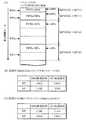
8.転送条件レジスタ(共用レジスタ)
本実施形態では図12に示すように、ホスト動作時には、パイプ領域PIPE0〜PIPEeとエンドポイントとの間で行われるデータ転送の転送条件情報(転送方向、転送種別、マックスパケットサイズ又はページ数等)が、転送条件レジスタTREG0〜TREGeに設定される。即ち、PIPE0、PIPEa、PIPEb、PIPEc、PIPEd、PIPEeの転送条件情報は、各々、TREG0、TREGa、TREGb、TREGc、TREGd、TREGeに設定(記憶)される。この設定は、例えばファームウェア(CPU)により行われる。
【0135】
そしてホストコントローラ50(広義には転送コントローラ)は、転送条件レジスタTREG0〜TREGeに設定された転送条件情報に基づいて、エンドポイントに対するトランザクションを発生する。そして、パイプ領域とそれに対応するエンドポイントとの間で、データ(パケット)を自動転送する。
【0136】
このように本実施形態では、各パイプ領域(バッファ領域)に対応して各転送条件レジスタが設けられ、この各転送条件レジスタに設定された転送条件情報に基づいて、各パイプ領域のパイプ転送(所与のデータ単位の転送)がホストコントローラ50により自動的に行われる。従って、ファームウェア(ドライバ、ソフトウェア)は、転送条件レジスタに転送条件情報を設定した後は、データ転送が完了するまで、データ転送制御に関わらなくて済むようになる。そして、所与のデータ単位のパイプ転送が完了すると割り込みが発生し、転送の完了がファームウェアに伝えられる。これにより、ファームウェア(CPU)の処理負荷を格段に低減できる。
【0137】
なお、本実施形態では図13に示すようにペリフェラル動作時には、エンドポイント領域EP0〜EPeとホストとの間で行われるデータ転送の転送条件情報(転送方向、転送種別、マックスパケットサイズ又はページ数等)が、転送条件レジスタTREG0〜TREGeに設定される。そしてペリフェラルコントローラ60(広義には転送コントローラ)は、転送条件レジスタTREG0〜TREGeに設定された転送条件情報に基づいて、エンドポイント領域とホストとの間でのデータ転送を行う。
【0138】
このように本実施形態では、転送条件レジスタTREG0〜TREGeが、ホスト動作時とペリフェラル動作時とで共用(兼用)される。これにより、レジスタ部70のリソースを節約でき、データ転送制御装置を小規模化できる。
【0139】
図14に、レジスタ部70のレジスタ構成例を示す。なお、レジスタ部70のレジスタの一部を、各ブロック(OTGC、HC、PC、Xcvr等)内に含ませてもよい。
【0140】
図14に示すように、レジスタ部70の転送条件レジスタ(TREG0〜TREGeの各々)は、ホスト動作時(HC、PIPE)とペリフェラル動作時(PC、EP)で共用されるHC/PC共用レジスタ(共用転送条件レジスタ)を含む。また、ホスト動作時にのみ使用されるHC(PIPE)用レジスタ(ホスト用転送条件レジスタ)を含む。また、ペリフェラル動作時にのみ使用されるPC(EP)用レジスタ(ペリフェラル用転送条件レジスタ)を含む。また、パケットバッファ(FIFO)のアクセス制御などを行うためのレジスタであり、ホスト動作時とペリフェラル動作時で共用されるアクセス制御レジスタを含む。
【0141】
例えば、デュアルロール・デバイスのホスト動作時に、ホストコントローラ50(HC)は、HC/PC共用レジスタとHC用レジスタに設定される転送条件情報に基づいて、データ(パケット)を転送する。
【0142】
一方、ペリフェラル動作時には、ペリフェラルコントローラ60(PC)は、HC/PC共用レジスタとPC用レジスタに設定される転送条件情報に基づいて、データ(パケット)を転送する。
【0143】
また、ホスト動作時、ペリフェラル動作時の両方において、バッファコントローラ80は、共用アクセス制御レジスタに基づいて、パケットバッファ100へのアクセス制御(リード/ライト・アドレスの発生、データのリード/ライト、アクセスの調停等)を行うことになる。
【0144】
図14のHC/PC共用レジスタには、データの転送方向(IN、OUT又はSETUP等)、転送種別(アイソクロナス、バルク、インタラプト、コントロールなどのトランザクションの種別)、エンドポイント番号(各USBデバイスのエンドポイントに関連づけられる番号)、マックスパケットサイズ(エンドポイントが送信又は受信可能なパケットの最大ペイロードサイズ。ページサイズ)が設定される。また、バッファ領域(パイプ領域、エンドポイント領域)のページ数(バッファ領域の面数)が設定される。また、DMA接続の有無(DMAハンドラ回路112によるDMA転送の使用の有無)を指示する情報が設定される。
【0145】
HC(PIPE)用レジスタには、インタラプト転送のトークン発行周期(インタラプト・トランザクションを起動する周期、インターバル)が設定される。また、トランザクションの連続実行回数(パイプ領域間の転送比率を設定する情報。各パイプ領域のトランザクションの連続実行回数)が設定される。また、ファンクションアドレス(エンドポイントを有するファンクションのUSBアドレス)、転送データのトータルサイズ(各パイプ領域を介して転送されるデータのトータルサイズ。IRPなどのデータ単位)が設定される。また、自動トランザクションの開始指示(ホストコントローラに対する自動トランザクション処理の開始指示)が設定される。また、自動コントロール転送モードの指示(コントロール転送のセットアップステージ、データステージ、ステータスステージのトランザクションを自動発生するモードの指示)が設定される。
【0146】
PC(EP)用レジスタには、エンドポイントイネーブル(エンドポイントのイネーブルやディスエーブルの指示)、ハンドシェーク指定(各トランザクションで行われるハンドシェークの指定)が設定される。
【0147】
パケットバッファ(FIFO)用の共用アクセス制御レジスタには、バッファ・I/Oポート(CPUによりPIO転送を行う場合のI/Oポート)が設定される。また、バッファ・フル/エンプティ(各バッファ領域のフル、エンプティの通知)、バッファ・残りデータサイズ(各バッファ領域の残りデータサイズ)が設定される。
【0148】
レジスタ部70は、インタラプト系レジスタ、ブロック系レジスタ、DMA制御レジスタなども含む。
【0149】
インタラプト系レジスタは、割り込みのステータス(要因)をCPUに対して示すためのインタラプト・ステータスレジスタ、割り込みのイネーブル、ディスエーブル(非マスク、マスク)を設定するインタラプト・イネーブルレジスタを含む。なお、割り込みには、OTGコントローラ20系、ホストコントローラ50系、ペリフェラルコントローラ60系の割り込みがある。
【0150】
ブロック系レジスタは、ブロック間で共用されるブロック間共用レジスタや、各ブロック(Xcvr、OTGC、HC、PC)内で使用されるブロック用レジスタを含む。
【0151】
ブロック間共用レジスタには、各ブロックのリセットを指示するレジスタなどがある。ブロック用レジスタには、トランシーバ10(Xcvr)を制御するためのレジスタや、OTGコントローラ20(OTGC)のステートコマンドレジスタや、ホストコントローラ50(HC)のステートコマンドレジスタや、フレーム番号を設定するレジスタなどがある。
【0152】
以上のように本実施形態では、ホスト動作時とペリフェラル動作時で共用されるレジスタ(HC/PC共用レジスタ、共用アクセス制御レジスタ)をレジスタ部70に設けている。これにより、ホスト動作時用のレジスタとペリフェラル動作時用のレジスタを全く別個に設ける場合に比べて、レジスタ部70を小規模化できる。また、CPU上で動作するファームウェア(ドライバ)から見た共用レジスタのアクセスアドレスを、ホスト動作時とペリフェラル動作時とで同一にできる。従って、ファームウェアは、これらの共用レジスタを同一アドレスで管理できるようになり、ファームウェア処理を簡素化できる。
【0153】
また、HC用レジスタや、PC用レジスタを設けることで、ホスト動作時(PIPE)の転送やペリフェラル動作時(EP)の転送に特有の転送条件を設定できる。例えば、トークン発行周期を設定することで、ホスト動作時にインタラプト転送のトークンを所望の周期で発行することが可能になる。また、連続実行回数を設定することで、ホスト動作時にパイプ領域間の転送比率を任意に設定できる。また、トータルサイズを設定することで、ホスト動作時にパイプ領域を介して自動転送されるデータのサイズを任意に設定できる。またファームウェアは、ホスト動作時に、自動トランザクションの開始を指示したり、自動コントロール転送モードのオン/オフを指示できるようになる。
【0154】
9.自動トランザクション
図15に、ホストコントローラ50の自動トランザクション(IN、OUT)処理時におけるファームウェア処理のフローチャート例を示す。
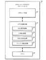
【0155】
まず、ファームウェア(処理部、ドライバ)は、図14等で説明した転送条件レジスタに転送条件情報(パイプ情報)を設定する(ステップS1)。より具体的には、転送データのトータルサイズ、マックスパケットサイズ(MaxPktSize)、ページ数(BufferPage)、転送方向(IN、OUT又はSETUP)、転送種別(アイソクロナス、バルク、コントロール、インタラプト)、エンドポイント番号、パイプ領域のトランザクションの連続実行回数(転送比率)、インタラプト転送のトークン発行周期などを、転送条件レジスタに設定する。
【0156】
次に、外部のシステムメモリとパケットバッファ100の間に転送経路を設定する(ステップS2)。即ち図4のDMAハンドラ回路112を介したDMA転送経路を設定する。
【0157】
次に、ファームウェアは、DMA転送の開始指示を行う(ステップS3)。即ち、図14のDMA制御レジスタのDMA転送開始指示ビットをアクティブにする。なお、CPUによる転送では、図14のバッファ・I/Oポートにアクセスすることで、パケットバッファ100にアクセスすることが可能になる。
【0158】
次に、ファームウェアは、自動トランザクションの開始指示を行う(ステップS4)。即ち、図14のHC用レジスタ(パイプレジスタ)の自動トランザクション開始指示ビットをアクティブにする。これにより、ホストコントローラ50による、自動トランザクション処理、パケット処理(パケットの生成、分解)、スケジューリング処理が行われる。即ち、ホストコントローラ50は、トータルサイズで指定されるデータを、マックスパケットサイズのペイロードのパケットを用いて、転送方向で指定される方向(IN、OUT)で、自動転送する。
【0159】
なお、ステップS3、S4の処理の順序は問わず、自動トランザクション開始指示の後にDMA転送の開始指示を行ってもよい。
【0160】
次に、ファームウェアは、パイプ転送の完了を知らせる割り込みが発生するのを待つ(ステップS5)。そして、割り込みが発生すると、ファームウェアは、図14のインタラプト系レジスタの割り込みステータス(要因)を調べる。そして、処理が正常完了又はエラー終了する(ステップS6)。
【0161】
このように本実施形態によれば、ファームウェアは、各パイプ領域毎に転送条件情報を設定し(ステップS1)、DMA転送開始の指示(ステップS3)と自動トランザクション開始の指示(ステップS4)を行うだけで、その後のデータ転送処理はホストコントローラ50のハードウェア回路により自動的に行われるようになる。従って、図3(A)、(B)で説明したOHCI準拠の手法に比べて、ファームウェアの処理負荷が軽減され、低性能のCPUが組み込まれる携帯機器に最適なデータ転送制御装置を提供できる。
【0162】
10.各ブロックの詳細な構成例
次に各ブロックの詳細な構成例について説明する。
【0163】
10.1 OTGコントローラ
図16に、OTGコントローラ20の構成例を示す。
【0164】
OTGコントローラ20は、OTGレジスタ部22を含む。このOTGレジスタ部22は、OTGコントローラ20のモニタレジスタや制御レジスタを含む。またファームウェア(CPU)により書き込まれるOTGステートコマンドをデコードする回路を含む。
【0165】
またOTGコントローラ20はOTG制御回路23を含む。そして、このOTG制御回路23は、OTGステートの管理を行うOTG管理回路24、IDピンの電圧レベルを検出するID検出回路25、VBUSの電圧レベルを検出するVBUS検出回路26、DP及びDMのラインステートを検出するラインステート検出回路27を含む。
【0166】
またOTGコントローラ20は、OTGステートの遷移判断条件の1つである時間を計測するタイマ28を含む。
【0167】
OTGステートを遷移させるために検出すべき情報は、ID、VBUSの電圧レベル、DP/DMのラインステートである。本実施形態のOTGコントローラ20は、これらの情報を検出し、モニタレジスタを介してファームウェア(CPU)に伝える。
【0168】
ファームウェアは、これらの検出情報に基づいて自身のステートを遷移させると共に、次に遷移すべきステートを、OTGステートコマンドを用いてOTGコントローラ20に伝える。
【0169】
OTGコントローラ20は、OTGステートコマンドをデコードし、そのデコード結果に基づいて、VBUSのドライブ制御、プルアップ/プルダウン抵抗の接続制御等を行い、図2(A)、(B)で説明したSRPやHNPを実現する。
【0170】
このように本実施形態では、ステート毎のOTG制御はOTGコントローラ20が担当し、ファームウェアはステートの遷移管理に専念できる。この結果、全てのステート制御をファームウェアで実現する場合に比べて、ファームウェア(CPU)の処理負荷を軽減できると共に、効率的なファームウェア開発が可能になる。
【0171】
なお、OTGのステート遷移の判断を、ファームウェアが行わずに、ハードウェア回路が行うようにしてもよい。或いは、OTGコントローラ20のほとんど全ての処理(例えばVBUS制御、プルアップ/プルダウン抵抗制御、ID検出、VBUS検出、ラインステート検出以外の処理)をファームウェア(ソフトウェア)により実現してもよい。
【0172】
10.2 ホストコントローラ、ペリフェラルコントローラ
図17(A)に、ホストコントローラ50の構成例を示す。
【0173】
ホストコントローラ50はHCシーケンス管理回路52を含む。このHCシーケンス管理回路52は、パイプ転送(パイプ領域を用いたデータ転送)の調停、時間管理、パイプ転送のスケジューリング、再送管理などを行う。
【0174】
より具体的にはHCシーケンス管理回路52は、フレーム番号のカウントや、SOF(Start-Of-Frame)パケットの送信指示を行う。また、アイソクロナス転送を各フレームの先頭で優先的に実行するための処理を行ったり、インタラプト転送をアイソクロナス転送の次に優先的に取り扱うための処理を行う。また、パイプ転送の順序に従って各パイプ転送を指示する処理を行う。また、トランザクションの連続実行回数を管理したり、残りフレーム時間の確認処理を行う。また、ペリフェラルから返ってきたハンドシェークパケット(ACK、NAK)に対する処理を行う。また、トランザクション実行時のエラー処理を行う。
【0175】
ホストコントローラ50はターゲットパイプ管理回路54を含む。このターゲットパイプ管理回路54は、レジスタ部70の転送条件レジスタに設定された転送条件情報のハンドリング処理などを行う。
【0176】
より具体的にはターゲットパイプ管理回路54は、転送条件情報の選択処理や、割り込み信号の生成処理を行う。また自動トランザクションの開始が指示された場合に、そのパイプ領域の転送データのトータルサイズをロードする。そして、残り転送データサイズのカウント(デクリメント)処理を行う。また、バッファコントローラ80へのデータの送受信の際にバッファ(FIFO)領域の状態を確認する処理を行う。また、トランザクション管理回路56への転送指示を行う。また、予期しないショートパケットの受信の判断処理や、マックスパケットサイズ以上のパケットの受信の判断処理を行う。また、零長パケットを自動転送するモードが設定されている場合には、最後の零長パケットの送信をトランザクション管理回路56に指示する。また、自動コントロール転送モードでのシーケンス管理を行う。
【0177】
ホストコントローラ50はトランザクション管理回路56を含む。このトランザクション管理回路56は、転送パケットの種類や転送順序の管理(トランザクションのシーケンス管理)を行う。また、タイムアウトの監視処理を行う。また、トランザクション終了の通知処理を行う。
【0178】
ホストコントローラ50はパケットハンドラ回路58を含む。このパケットハンドラ回路58は、パケットの生成、分解処理を行う。また、PIDのチェックやCRCのデコード、エンコードを行う。また、バッファ領域のパケットのペイロードのリード、ライト処理や、SOFパケットの送信処理を行う。また、送受信データのカウント処理を行う。
【0179】
図17(B)にペリフェラルコントローラ60の構成例を示す。
【0180】
ペリフェラルコントローラ60は、トランザクション管理回路62、パケットハンドラ回路64を含む。これらのトランザクション管理回路62、パケットハンドラ回路64は、ホストコントローラ50のトランザクション管理回路56、パケットハンドラ回路58とほぼ同様の処理を行う。
【0181】
10.3 バッファコントローラ
図18にバッファコントローラ80の構成例を示す。
【0182】
バッファコントローラ80は領域確保(allocation)回路82を含む。この領域確保回路82は、パケットバッファ100に、バッファ領域(ホスト動作時にパイプ領域に設定され、ペリフェラル動作時にエンドポイント領域に設定される領域)を確保する回路である。
【0183】
領域確保回路82は領域計算回路83を含む。この領域計算回路83は、マックスパケットサイズ(広義にはページサイズ)やページ数に基づいて、バッファ領域の領域サイズ、スタートアドレス、エンドアドレスなどを計算する回路である。
【0184】
例えば図19(A)に示すバッファ領域PIPE0/EP0、PIPEa/EPa、PIPEb/EPb、PIPEc/EPcでは、マックスパケットサイズ(MaxPktSize)が、各々、32、64、64、64バイトに設定され、ページ数(BufferPage)が、各々、1、1、3、2ページに設定されている。領域計算回路83は、これらのマックスパケットサイズ、ページ数などに基づいて、バッファ領域PIPE0/EP0〜PIPEc/EPcの領域サイズ、スタートアドレス、エンドアドレスを計算する。例えば図19(A)において、PIPE0/EP0、PIPEa/EPa、PIPEb/EPb、PIPEc/EPcの領域サイズは、各々、32(=32×1)、64(=64×1)、192(=64×3)、128(=64×2)バイトと計算されることになる。
【0185】
ポインタ割り当て回路84は、各バッファ領域の書き込みポインタWP(WP0、WPa、WPb、WPc)、読み出しポインタRP(RP0、RPa、RPb、RPc)を、DMA用ポインタ、CPU用ポインタ、USB用ポインタに割り当てる回路である。
【0186】
例えば図19(B)に示すように、データ送信時(DMA又はCPUからパケットバッファ100を介してUSB側にデータが転送される時)であり、且つ、DMA転送使用時には、そのバッファ領域の書き込みポインタWPはDMA(DMAアクセス)用のポインタに割り当てられ、読み出しポインタRPはUSB(USBアクセス)用のポインタに割り当てられる。また、データ送信時であり且つCPU(PIO)転送使用時には、そのバッファ領域の書き込みポインタWPはCPU(CPUアクセス)用のポインタに割り当てられ、読み出しポインタRPはUSB用のポインタに割り当てられる。
【0187】
一方、図19(C)に示すように、データ受信時(USBからパケットバッファ100を介してDMA又はCPU側にデータが転送される時)であり、且つ、DMA転送使用時には、そのバッファ領域の書き込みポインタWPはUSB用ポインタに割り当てられ、読み出しポインタRPはDMA用ポインタに割り当てられる。また、データ受信時であり且つCPU転送使用時には、そのバッファ領域の書き込みポインタWPはUSB用ポインタに割り当てられ、読み出しポインタRPはCPU用ポインタに割り当てられる。
【0188】
なお、各バッファ領域の書き込みポインタWP、読み出しポインタRPのポインタ情報(位置情報)は、レジスタ部70の各転送条件レジスタ(PIPE/EPレジスタ)に保持される。
【0189】
ポインタ管理回路86は、ポインタの更新を行いながら、パケットバッファ100にアクセスするための実アドレスを生成する回路である。
【0190】
ポインタ管理回路86は、CPU用アドレス生成回路87、DMA用アドレス生成回路88、USB用アドレス生成回路89を含む。これらの生成回路87、88、89は、各々、ポインタ割り当て回路84により割り当てられたCPU用ポインタ、DMA用ポインタ、USB用ポインタに基づいて、CPU用アドレス、DMA用アドレス、USB用アドレスを生成する。また、CPU(CPUインターフェース回路)、DMA(DMAハンドラ回路)からのアクセス毎に、或いはUSB(HC又はPC)のトランザクション終了(ACK、NAKなどのハンドシェーク送受信)毎に、ポインタを更新する処理を行う。なお、更新後のポインタの情報は、領域確保回路82を介してレジスタ部70の各転送条件レジスタに書き戻される。
【0191】
バッファ管理回路90は、パケットバッファ100へのアクセスを管理する回路である。
【0192】
バッファ管理回路90はバッファインターフェース回路92を含む。このバッファインターフェース回路92は、ポインタ管理回路86からのCPU用アドレス、DMA用アドレス、USB用アドレスなどを受け、パケットバッファ100へのデータの入出力や、アドレス、出力イネーブル、ライトイネーブル、リードイネーブルなどの出力を行う。
【0193】
バッファ管理回路90は調停回路93を含む。この調停回路93は、CPU(CPUインターフェース回路)、DMA(DMAハンドラ回路)、USB(ホストコントローラ又はペリフェラルコントローラ)からのアクセスを調停する回路である。この調停結果に基づいて、CPU用アドレス、DMA用アドレス、USB用アドレスのいずれかが、パケットバッファ100のアクセス・アドレスとして出力され、CPU、DMA又はUSBとパケットバッファ100との間のデータ転送経路が設定される。
【0194】
HC/PCセレクタ94は、バッファ管理回路90(バッファコントローラ80)とホストコントローラ50(HC)又はペリフェラルコントローラ60(PC)との間の接続の切り替え制御を行う。例えばホスト動作時には、ホストコントローラ50とバッファ管理回路90を接続し、ペリフェラル動作時には、ペリフェラルコントローラ60とバッファ管理回路90を接続する。なお、この接続の切り替え制御は、OTGコントローラ20(OTGC)からのHC/PCイネーブル信号に基づいて行う。
【0195】
11.電子機器
次に、本実施形態のデータ転送制御装置を含む電子機器の例について説明する。
【0196】
例えば図20(A)に電子機器の1つであるプリンタの内部ブロック図を示し、図21(A)にその外観図を示す。CPU510(処理部)はシステム全体の制御などを行う。操作部511はプリンタをユーザが操作するためのものである。ROM516には、制御プログラム、フォントなどが格納され、RAM517(システムメモリ)はCPU510のワーク領域として機能する。DMAC518は、CPU510を介さずにデータ転送を行うためのDMAコントローラである。表示パネル519はプリンタの動作状態をユーザに知らせるためのものである。
【0197】
USBを介してパーソナルコンピュータ、デジタルカメラ、デジタルビデオカメラなどの他の機器から送られてきたシリアルの印刷データ(印字データ、画像データ)は、データ転送制御装置500によりパラレルの印刷データに変換される。そして、変換後のパラレル印刷データは、CPU510又はDMAC518により、印刷処理部(プリンタエンジン)512に送られる。そして、印刷処理部512においてパラレル印刷データに対して所与の処理が施され、プリントヘッダなどからなる印刷部(データの出力処理を行う装置)514により紙に印刷されて出力される。
【0198】
図20(B)に電子機器の1つであるデジタルカメラの内部ブロック図を示し、図21(B)にその外観図を示す。CPU520はシステム全体の制御などを行う。操作部521(シャッターボタン、操作ボタン等)はデジタルカメラをユーザが操作するためのものである。ROM526には制御プログラムなどが格納され、RAM527はCPU520のワーク領域として機能する。DMAC528はDMAコントローラである。
【0199】
CCD、レンズなどからなる撮像部(データの取り込み処理を行う装置)522により画像が撮像され、撮像された画像のデータは画像処理部524により処理される。そして、処理後の画像データは、CPU520又はDMAC528によりデータ転送制御装置500に送られる。データ転送制御装置500は、このパラレルの画像データをシリアルデータに変換し、USBを介してプリンタ、ストレージ装置、パーソナルコンピュータなどの他の機器に送信する。
【0200】
図20(C)に電子機器の1つであるCD−RWドライブ(ストレージ装置)の内部ブロック図を示し、図21(C)にその外観図を示す。CPU530はシステム全体の制御などを行う。操作部531はCD−RWをユーザが操作するためのものである。ROM536には制御プログラムなどが格納され、RAM537はCPU530のワーク領域として機能する。DMAC538はDMAコントローラである。
【0201】
レーザ、モータ、光学系などからなる読み取り&書き込み部(データの取り込み処理を行う装置又はデータの記憶処理を行うための装置)533によりCD−RW532から読み取られたデータは、信号処理部534に入力され、エラー訂正処理などの所与の信号処理が施される。そして、信号処理が施されたデータが、CPU530又はDMAC538によりデータ転送制御装置500に送られる。データ転送制御装置500は、このパラレルのデータをシリアルデータに変換し、USBを介して他の機器に送信する。
【0202】
一方、USBを介して他の機器から送られてきたシリアルのデータは、データ転送制御装置500によりパラレルのデータに変換される。そして、このパラレルデータは、CPU530又はDMAC538により信号処理部534に送られる。そして、信号処理部534においてこのパラレルデータに対して所与の信号処理が施され、読み取り&書き込み部533によりCD−RW532に記憶される。
【0203】
なお、図20(A)、(B)、(C)において、CPU510、520、530の他に、データ転送制御装置500でのデータ転送制御のためのCPUを別に設けるようにしてもよい。
【0204】
本実施形態のデータ転送制御装置を電子機器に用いれば、OTG機能を有する電子機器を実現できる。即ち、電子機器にホストとしての役割を持たせたり、デバイスとしての役割を持たせることが可能になり、これまでに存在しなかったアプリケーションを創出できる。
【0205】
また本実施形態のデータ転送制御装置を電子機器に用いれば、電子機器に組み込まれるCPU(処理部)の処理負荷が軽減され、安価なCPUを用いることが可能になる。また、CPUが、データ転送制御処理以外の他の処理を余裕を持って行うことが可能になり、電子機器の性能向上や低コスト化を図れる。また、CPU上で動作するファームウェアのプログラムを簡素化でき、電子機器の開発期間の短縮化を図れる。
【0206】
なお本実施形態のデータ転送制御装置を適用できる電子機器としては、上記以外にも例えば、種々の光ディスクドライブ(CD−ROM、DVD)、光磁気ディスクドライブ(MO)、ハードディスクドライブ、デジタルビデオカメラ、携帯電話、スキャナ、TV、VTR、オーディオ機器、電話機、プロジェクタ、パーソナルコンピュータ、電子手帳、或いはワードプロセッサなど種々のものを考えることができる。
【0207】
なお、本発明は本実施形態に限定されず、本発明の要旨の範囲内で種々の変形実施が可能である。
【0208】
例えば、本発明のデータ転送制御装置の構成は、図4等で説明した構成に限定されるものではなく、種々の変形実施が可能である。
【0209】
また、データ転送制御装置の各ブロック(HC、PC、OTGC等)の構成も、本実施形態で説明したものに限定されず、種々の変形実施が可能である。
【0210】
また、SOFパケットの周期転送を無効にする回路も、図10に示す構成に限定されず、種々の変形実施が可能である。
【0211】
また、本発明のSOFパケットは、その名称は問わず、SOFパケットと同等の機能を有するパケット(フレーム開始を指示、管理するパケット)であればよい。
【0212】
また、明細書中の記載において広義な用語(非周期転送、周期転送、第1のモード、第2のモード、ステートコントローラ、処理部、転送コントローラ、バス、バッファ領域等)として引用された用語(バルク転送、アイソクロナス転送、SOF有りモード、SOF無しモード、OTGコントローラ、CPU・ファームウェア、ホストコントローラ・ペリフェラルコントローラ、USB、パイプ領域・エンドポイント領域等)は、明細書中の他の記載においても広義な用語に置き換えることができる。
【0213】
また、本発明のうち従属請求項に係る発明においては、従属先の請求項の構成要件の一部を省略する構成とすることもできる。また、本発明の1の独立請求項に係る発明の要部を、他の独立請求項に従属させることもできる。
【0214】
また、本実施形態ではUSBのOTG規格への適用例を説明したが、本発明が適用されるのはOTG規格に限定されない。即ち、USBのOTGのみならず、従来のUSB1.1、USB2.0や、これらの規格を発展させた規格におけるデータ転送にも本発明は適用できる。
【図面の簡単な説明】
【図1】図1(A)、(B)、(C)は、USBのOTG規格について説明するための図である。
【図2】図2(A)、(B)は、SRPやHNPの手順について説明するための図である。
【図3】図3(A)、(B)は、OHCIのリスト構造のディスクリプタなどについて説明するための図である。
【図4】本実施形態のデータ転送制御装置の構成例を示す図である。
【図5】図5(A)、(B)は、パイプ領域、エンドポイント領域について説明するための図である。
【図6】図6(A)、(B)は、SOFパケットについて説明するための図である。
【図7】SOF有りモード(第1のモード)設定時の信号波形例である。
【図8】SOF無しモード(第2のモード)設定時の信号波形例である。
【図9】SOF無しモードに設定され、且つ、転送すべきデータが無い場合の信号波形例である。
【図10】SOFパケットの周期転送を無効にする回路の構成例である。
【図11】図11(A)、(B)は、図10の回路の動作を説明するための真理値表である。
【図12】データ転送制御装置のホスト時の動作について説明するための図である。
【図13】データ転送制御装置のペリフェラル時の動作について説明するための図である。
【図14】レジスタ部について説明するための図である。
【図15】ファームウェアの処理例を説明するためのフローチャートである。
【図16】OTGコントローラの詳細な構成例を示す図である。
【図17】図17(A)、(B)は、ホストコントローラ、ペリフェラルコントローラの詳細な構成例を示す図である。
【図18】バッファコントローラの詳細な構成例を示す図である。
【図19】図19(A)、(B)、(C)は、領域確保手法やポインタ割り当て手法について説明するための図である。
【図20】図20(A)、(B)、(C)は、種々の電子機器の内部ブロック図の例である。
【図21】図21(A)、(B)、(C)は、種々の電子機器の外観図の例である。
【符号の説明】
PIPE0〜PIPEe パイプ(バッファ)領域
EP0〜EPe エンドポイント(バッファ)領域
TREG0〜TREGe 転送条件レジスタ(共用レジスタ)
10 トランシーバ
12 物理層回路
20 OTGコントローラ(ステートコントローラ)
30 HC/PC切り替え回路
32 HC/PCセレクタ
34 ラインステートコントローラ
40 転送コントローラ
50 ホストコントローラ
60 ペリフェラルコントローラ
70 レジスタ部
72 転送条件レジスタ部(共用レジスタ)
80 バッファコントローラ
100 パケットバッファ(FIFO、RAM)
110 インターフェース回路
112 DMAハンドラ回路
114 CPUインターフェース回路
120 クロックコントローラ[0001]
BACKGROUND OF THE INVENTION
The present invention relates to a data transfer control device, an electronic device, and a data transfer control method.
[0002]
[Background Art and Problems to be Solved by the Invention]
While the USB (Universal Serial Bus) 2.0 market is steadily expanding, an interface standard called USB On-The-Go (OTG) has been formulated by the USB Implementers Forum (USB-IF). The OTG standard (OTG1.0) formulated in the form of extending USB 2.0 has the potential to create new added value of the USB interface, and the appearance of applications that take advantage of its characteristics is awaited.
[0003]
According to this OTG, a peripheral (peripheral device) that has been connected to a host (personal computer or the like) via a USB can be provided with a host function. As a result, it is possible to transfer data by connecting peripherals to each other via USB. For example, it is possible to directly connect a digital camera and a printer to print an image of the digital camera. In addition, data can be stored by connecting a digital camera or digital video camera to the storage device.
[0004]
However, a peripheral having a host function by OTG generally incorporates a low-performance CPU (processing unit). Therefore, if the CPU (firmware) processing load of the peripheral becomes heavy due to the addition of the host function or the processing becomes complicated, other processing may be hindered or the device design period may be prolonged. Arise.
[0005]
The USB standards such as USB 1.1, USB 2.0, and OTG define four transfer types: isochronous transfer, bulk transfer, control transfer, and interrupt transfer. The USB host manages the transfer order of these transfer type packets, and transfers the transfer type packets in consideration of the remaining frame time. For this purpose, in USB, the host performs frame management, and the host generates a SOF (Start Of Frame) packet every 1 ms for FS (Full Speed) and LS (Low Speed), and every 125 μs for HS (High Speed). Transfer to (device).
[0006]
However, in non-periodic transfer such as bulk transfer and control transfer, it has been found that the transfer of such SOF packets results in narrowing the bus bandwidth, resulting in a decrease in transfer efficiency.
[0007]
The present invention has been made in view of the technical problems as described above, and an object of the present invention is to provide a data transfer control device, an electronic device, and a data transfer control method capable of improving transfer efficiency during non-periodic transfer. It is to provide.
[0008]
[Means for Solving the Problems]
The present invention is a data transfer control device for data transfer via a bus, comprising: a buffer controller that controls access to a packet buffer that stores transfer data; and a transfer controller that controls transfer of data in the packet buffer. And when the first mode is set, the transfer controller performs data transfer while transferring a SOF (Start Of Frame) packet at a frame period, and the second mode is set and an aperiodic transfer is performed. When performing, it relates to a data transfer control device that disables periodic transfer of SOF packets and transfers aperiodic data.
[0009]
In the present invention, when the first mode is set, data transfer is performed while the SOF packet is transferred in a frame cycle. This makes it possible to properly perform periodic transfer such as isochronous transfer. On the other hand, when the second mode is set, the transfer of the SOF packet is invalidated and the transfer of aperiodic data is performed. As a result, it is possible to generate a transaction across the boundaries of a plurality of frames, and the transfer efficiency of aperiodic transfer such as bulk transfer and control transfer can be improved.
[0010]
In the present invention, when there is no aperiodic data to be transferred, the transfer controller may transfer the SOF packet at the frame period even when the second mode is set.
[0011]
In this way, it is possible to prevent a situation in which another device connected to the bus shifts to an inappropriate state. Whether or not there is aperiodic data to be transferred can be determined by, for example, a transfer start instruction signal, a packet buffer full, an empty signal, or the like.
[0012]
Further, the present invention includes a state controller that controls a plurality of states including a host operation state that operates as a host role and a peripheral operation state that operates as a peripheral role, and the packet buffer includes each endpoint. A plurality of pipe areas in which data transferred between each of the pipe areas is stored are secured, and when the transfer controller is in host operation, a host controller that performs data transfer as a host, and in peripheral operation, A peripheral controller that transfers data as a peripheral, and the host controller automatically generates a transaction for an endpoint and automatically transfers data between the pipe area and the endpoint corresponding to the pipe area. In It may be.
[0013]
According to the present invention, for example, when the state controlled by the state controller becomes the host operation state, the host controller performs data transfer as the role of the host. When the state controlled by the state controller becomes a peripheral operation state, the peripheral controller performs data transfer as a role of the peripheral. As a result, a so-called dual-role device function can be realized.
[0014]
In the present invention, during host operation, a plurality of pipe areas are allocated to the packet buffer, and data is automatically transferred between the reserved pipe areas and the endpoints. As a result, a dual-role device function can be realized and the processing load on the processing unit during host operation can be reduced.
[0015]
In the present invention, when the second mode is set, the host controller invalidates the periodic transfer of the SOF packet between the pipe area and the aperiodic transfer end point corresponding to the pipe area. However, the aperiodic data may be automatically transferred.
[0016]
In this way, it is possible to automatically transfer aperiodic data to / from an aperiodic transfer end point using the pipe region, and the data transfer can be made more efficient. At this time, according to the present invention, since the periodic transfer of the SOF packet becomes invalid, the data transfer can be made more efficient. When disabling SOF packet transfer (when setting to the second mode), an endpoint of a transfer type other than periodic transfer (such as isochronous transfer) is allocated to the pipe area reserved in the packet buffer. It is desirable.
[0017]
In the present invention, when the automatic transfer instruction signal of the pipe area is all inactive, the host controller automatically transfers the SOF packet at the frame period even when the second mode is set. Also good.
[0018]
In this way, since it can be determined based on the automatic transfer instruction signal whether there is data to be transferred, the determination process can be simplified. Then, when all the automatic transfer instruction signals are inactive (when there is no data to be transferred), other devices connected to the bus shift to an inappropriate state by transferring the SOF packet. Etc. can be prevented.
[0019]
In the present invention, the host controller activates an SOF transfer start trigger for each frame period, and deactivates the SOF transfer start trigger when the SOF packet transfer is completed, and a pipe An SOF invalid signal generation circuit for receiving an automatic transfer instruction signal for a region, a state information signal from the state controller, and a signal for instructing the first or second mode, and generating a signal for invalidating the SOF transfer start trigger; May be included.
[0020]
In this way, processing for invalidating the transfer of the SOF packet can be realized with a simple circuit. For example, when the state indicated by the state information signal is the host operation, the second mode is instructed, and at least one of the automatic transfer instruction signals is active, the invalid signal of the SOF transfer start trigger is activated, Generation of the SOF transfer start trigger can be disabled. On the other hand, when the state indicated by the state information signal is a host operation and the second mode is instructed, if all the automatic transfer instruction signals are inactive (there is no data to be transferred), SOF transfer is performed. The start trigger invalid signal can be deactivated to prevent the generation of the SOF transfer start trigger from being invalidated.
[0021]
Also, in the present invention, during the peripheral operation, a plurality of endpoint areas where data transferred to and from the host is stored in each endpoint area are secured in the packet buffer, and the peripheral controller is connected to the endpoint area and the host. You may make it transfer data between.
[0022]
In this way, the buffer area of the packet buffer can be used as a pipe area during a host operation, and can be used as an endpoint area during a peripheral operation. As a result, it is possible to effectively use the resource of the packet buffer and reduce the processing load of the processing unit.
[0023]
In the present invention, the aperiodic transfer may be USB (Universal Serial Bus) standard bulk transfer or control transfer, and the aperiodic data may be bulk data or control data.
[0024]
In the present invention, data transfer conforming to the USB (Universal Serial Bus) OTG (On-The-Go) standard may be performed.
[0025]
According to another aspect of the present invention, there is provided a data transfer control device according to any one of the above, an apparatus that performs an output process, a capture process, or a storage process of data transferred via the data transfer control apparatus and a bus, and the data transfer control apparatus. The present invention relates to an electronic device including a processing unit that controls data transfer.
[0026]
The present invention also relates to a data transfer control method for data transfer via a bus, wherein access control of a packet buffer for storing transfer data is performed to control transfer of data in the packet buffer, and the first mode Is set, the data transfer is performed while transferring the SOF (Start Of Frame) packet at the frame period. When the second mode is set and the non-periodic transfer is performed, the SOF packet is periodically transferred. The present invention relates to a data transfer control method for invalidating and transferring aperiodic data.
[0027]
DETAILED DESCRIPTION OF THE INVENTION
Hereinafter, this embodiment will be described.
[0028]
In addition, this embodiment demonstrated below does not unduly limit the content of this invention described in the claim. Further, not all of the configurations described in the present embodiment are essential as a solution means of the present invention.
[0029]
1. OTG
First, OTG (USB On-The-Go) will be briefly described.
[0030]
1.1 A device, B device
In OTG, a Mini-A plug and a Mini-B plug as shown in FIG. 1A are defined as connector standards. In addition, a Mini-AB receptacle is defined as a connector that can connect both of these Mini-A plugs and Mini-B plugs (first and second plugs of the cable in a broad sense).
[0031]
For example, as shown in FIG. 1B, when the electronic device P is connected to the Mini-A plug of the USB cable and the electronic device Q is connected to the Mini-B plug, the electronic device P is set to the A device, The electronic device Q is set as the B device. On the other hand, as shown in FIG. 1C, when the Mini-B plug and Mini-A plug are connected to the electronic devices P and Q, the electronic devices P and Q are set to the B device and the A device, respectively. The
[0032]
In the Mini-A plug, the ID pin is connected to GND, and in the Mini-B plug, the ID pin is in a floating state. The electronic device detects whether it is connected to the Mini-A plug or the Mini-B plug by detecting the voltage level of this ID pin using the built-in pull-up resistor circuit. To do.
[0033]
In OTG, the A device (master) is the side (supplier) that supplies power (VBUS), and the B device (slave) is the side that receives power (supplier). The default state of the A device is a host, and the default state of the B device is a peripheral (peripheral device).
[0034]
1.2 Dual-role device
In OTG, a dual-role device is defined which can have both a role as a host (simple host) and a role as a peripheral.
[0035]
Dual-role devices can be either hosts or peripherals. When the partner connected to the dual-role device is a host or peripheral in the conventional USB standard, the role of the dual-role device is uniquely determined. That is, if the connection partner is a host, the dual-role device becomes a peripheral, and if the connection partner is a peripheral, the dual-role device becomes a host.
[0036]
On the other hand, if the connection partner is a dual-role device, both dual-role devices can exchange host and peripheral roles with each other.
[0037]
1.3 SRP, HNP
The dual-role device has functions of a session start request procedure SRP (Session Request Protocol) and a host exchange procedure HNP (Host Negotiation Protocol) as shown in FIGS.
[0038]
Here, the session start request procedure SRP is a protocol in which the B device requests the A device to supply VBUS (power).
[0039]
In the case of not using the bus, in the OTG, the A device can stop supplying the VBUS. Thereby, when the A device is, for example, a small portable device, wasteful power consumption can be prevented. Then, when the B device wants the V device to supply the VBUS after the A device stops supplying the VBUS, this SRP is used to request the A device to resume the supply of the VBUS.
[0040]
FIG. 2A shows the flow of SRP. As shown in FIG. 2A, the B device requests the A device to supply VBUS by performing data line pulsing and VBUS pulsing. Then, after the supply of VBUS by the A device, the peripheral operation of the B device (peripheral operation) and the host operation of the A device (host operation) start.
[0041]
As described in FIGS. 1 (A) to 1 (C), in the connection between dual-role devices, the A device on the side to which the Mini-A plug is connected becomes the default host, and the Mini-B plug is The connected B device becomes the default peripheral. In OTG, the roles of the host and the peripheral can be exchanged without plugging and unplugging. HNP is a protocol for exchanging the roles of this host and peripheral.
[0042]
The flow of HNP is shown in FIG. When the A device operating as the default host finishes using the bus, the bus becomes idle. After that, when the B device disables the pull-up resistor of the data signal line DP (D +), the A device enables the DP pull-up resistor. As a result, the role of the A device is changed from the host to the peripheral, and the operation as the peripheral is started. In addition, the role of the B device is changed from the peripheral to the host, and the operation as the host is started.
[0043]
After that, when the B device finishes using the bus and the A device disables the DP pull-up resistor, the B device enables the DP pull-up resistor. Thereby, the role of the B device returns from the host to the peripheral, and the operation as the peripheral is resumed. Also, the role of the A device returns from the peripheral to the host and resumes the operation as the host.
[0044]
According to the OTG described above, a portable device such as a cellular phone or a digital camera can be operated as a USB host, and data can be transferred by connecting the portable devices with each other in a peer-to-peer manner. As a result, a new added value can be created in the USB interface, and an application that has not existed before can be created.
[0045]
2. OHCI
In the conventional USB, the data transfer control device (host controller) of the personal computer that is the host complies with standards such as OHCI (Open Host Controller Interface) and UHCI (Universal Host Controller Interface) proposed by Microsoft. It was. Also, the OS (Operating System) used is limited to Microsoft Windows and Apple Macintosh OS.
[0046]
However, in a small portable device that is a target application of OTG, the architecture of the CPU to be incorporated and the OS used are various. Furthermore, OHCI and UHCI standardized for a host controller of a personal computer are premised on full implementation of functions as a USB host, and are not optimal for mounting on small portable devices.
[0047]
For example, FIG. 3A shows an example of a descriptor having a list structure used in OHCI.
[0048]
In FIG. 3A, endpoint descriptors ED1, ED2, and ED3 are linked by link pointers, and contain information necessary for communication with
[0049]
The descriptor having the list structure in FIG. 3A is created by firmware (host controller / driver) operating on the CPU 610 (processor in a broad sense) in FIG. 3B and written in the
[0050]
The data transfer control device 600 (host controller) reads the descriptor having the list structure written in the
[0051]
Specifically, the data transfer control device 600 (host controller) sets information on the
[0052]
As described above, in an OHCI-compliant data transfer control device (host controller), firmware (host controller / driver) operating on the CPU must create a descriptor having a complicated structure as shown in FIG. I must. Therefore, the processing load on the CPU is very heavy.
[0053]
In this case, in the conventional USB, only a personal computer is assigned the host role, and this personal computer has a high-performance CPU. Therefore, it is possible to create a descriptor having a complicated structure as shown in FIG.
[0054]
However, a CPU (embedded CPU) incorporated in a small portable device (digital camera, mobile phone, etc.), which is an OTG target application, generally has a significantly lower performance than a personal computer CPU. Accordingly, if the OTG host operation is performed in the portable device, an excessive load is applied to the CPU incorporated in the portable device, which causes problems such as troubles in other processes and a decrease in data transfer performance.
[0055]
3. Configuration example
FIG. 4 shows a configuration example of the data transfer control device of this embodiment that can solve the above-described problems. Note that the data transfer control device of this embodiment does not have to include all the circuit blocks in FIG. 4, and some of the circuit blocks may be omitted.
[0056]
The transceiver 10 (hereinafter referred to as Xcvr as appropriate) is a circuit that transmits and receives USB (bus in a broad sense) data using differential data signals DP and DM, and includes a USB physical layer (PHY)
[0057]
The OTG controller 20 (state controller in a broad sense, hereinafter referred to as OTGC as appropriate) performs various processes for realizing the STG function and the HNP function (see FIGS. 2A and 2B) of the OTG. That is, the
[0058]
More specifically, the OTG standard defines a state transition at the time of the A device of the dual role device (see FIGS. 1B and 1C) and a state transition at the time of the B device. The
[0059]
The HC / PC switching circuit 30 (HC / PC / common circuit) controls switching of connection between the
[0060]
For example, when the
[0061]
The
[0062]
Here, the
[0063]
That is, the
[0064]
More specifically, the
[0065]
On the other hand, the
[0066]
That is, the
[0067]
More specifically, the
[0068]
An end point is a point (part) on a peripheral (device) to which a unique address can be assigned. All data transfer between the host and the peripheral (device) is performed via this endpoint. The transaction is composed of a token packet, an optional data packet, and an optional handshake packet.
[0069]
The
[0070]
The
[0071]
During the peripheral operation, the endpoint area (EP0 to EPe) is secured in the
[0072]
The buffer controller 80 (FIFO manager) performs access (read / write) control and area management for the
[0073]
For example, during host operation, the
[0074]
On the other hand, during the peripheral operation, the
[0075]
The packet buffer 100 (FIFO, packet memory, buffer) temporarily stores (buffers) data (transmission data or reception data) transferred via the USB. The
[0076]
During host operation, the
[0077]
On the other hand, during the peripheral operation, the
[0078]
Note that the buffer area secured in the packet buffer 100 (the area set in the pipe area during the host operation and the end point area during the peripheral operation) is stored such that the previously input information is output first. It is set in the area (FIFO area).
[0079]
PIPE0 is a pipe area dedicated to the
[0080]
That is, in USB, the
[0081]
In this embodiment, the buffer area (pipe area or endpoint area) is set by the maximum packet size MaxPktSize (page size in a broad sense) and the number of pages BufferPage (RSize = MaxPktSize × BufferPage). . In this way, the area size and the number of pages (number of pages) of the buffer area can be arbitrarily set, and the resources of the
[0082]
The
[0083]
The
[0084]
4). Pipe area
In this embodiment, as shown in FIG. 5A, pipe areas PIPE0 to PIPEe are allocated in the
[0085]
Here, the “pipe” in the pipe area of this embodiment is a “pipe” defined by USB (a logical abstraction representing a relationship between an endpoint on a device and software on a host, a logical Route) is slightly different in meaning.
[0086]
As shown in FIG. 5A, the pipe area of the present embodiment is secured on the
[0087]
In the example of FIG. 5A, USB bulk IN transfer is performed between the pipe region PIPEa and the
[0088]
As described above, in the present embodiment, arbitrary data transfer (isochronous transfer, bulk transfer, interrupt transfer) can be performed between a pipe area (general-purpose) and the corresponding endpoint.
[0089]
In this embodiment, data in a given data unit (a data unit specified by the total size) is transferred between the pipe area and the corresponding endpoint. As a data unit in this case, for example, a data unit requested to be transferred by an IRP (I / O request packet) or a data unit obtained by dividing the data unit into an appropriate size can be considered. This data unit data transfer (a series of transactions) to the endpoint can be called a “pipe” in the present embodiment. An area for storing such “pipe” data (transmission data, reception data) is a pipe area.
[0090]
When the transfer of a given data unit using the pipe area is completed, the pipe area can be released. The released pipe area can be assigned to an arbitrary endpoint. As described above, in this embodiment, the association between the pipe region and the end point can be dynamically changed.
[0091]
In the present embodiment, as shown in FIG. 5B, the endpoint areas EP0 to EPe are secured (set) in the
[0092]
As described above, in this embodiment, the buffer area of the
[0093]
The number of pipe regions and endpoint regions is not limited to six and is arbitrary.
[0094]
5. No SOF mode (Transfer only bulk without SOF mode)
Now, in the USB standard (USB1.1, USB2.0, OTG, etc.), four types of transfer types (isochronous, bulk, control, interrupt) are defined. The USB host controls and manages the transfer order of these transfer type packets, and instructs transfer of each transfer type packet. For this purpose, in USB, the host performs frame management, and, as shown in FIG. 6A, issues an SOF (Start Of Frame) packet to the peripheral for each frame (1 ms, 125 μs).
[0095]
The SOF is a token packet for indicating the head of the frame, and includes a PID, a frame number, and a CRC. This SOF is transmitted by the host. The host performs scheduling management so that one transaction does not extend over a plurality of frames. The frame is an interval between the SOF and the next SOF. Bulk transfer is a method for aperiodically transferring a large amount of data such as print data and image data.
[0096]
In isochronous transfer and interrupt transfer, which are periodic (synchronous) transfers, information such as frame timing and frame number is important. Therefore, an SOF packet is required to transmit these pieces of information.
[0097]
On the other hand, in bulk transfer and control transfer, which are non-periodic transfers, it is considered that these pieces of information are not particularly necessary. However, in USB, in the case of such non-periodic transfer, the host transfers the SOF packet. Demands.
[0098]
However, when an SOF packet is transferred in aperiodic transfer such as bulk transfer, the bus bandwidth is consumed by the transfer of the SOF packet itself. Furthermore, as shown in FIG. 6B, in the USB, the presence of this SOF packet causes a transfer prohibition period (transfer prohibition area) at the end of the frame, which further narrows the bus bandwidth.
[0099]
The USB is widely used for transfer of print data of a printer, transfer of image data of a digital camera, transfer of storage data of a storage device, etc. Bulk transfer is used for transferring these data. Therefore, in this bulk transfer, if the bus bandwidth is narrowed by an SOF packet that is not originally required, resources are wasted.
[0100]
Therefore, in the present embodiment, a technique is adopted in which the transfer of the SOF packet (packet instructing the start of the frame) is canceled in aperiodic transfer such as bulk transfer.
[0101]
More specifically, when the mode with SOF (first mode in a broad sense) is set, data transfer is performed while transferring the SOF packet (SOF token packet) at the frame period. On the other hand, when the non-SOF mode (second mode in a broad sense) is set and aperiodic transfer (bulk transfer or control transfer) is performed, the periodic transfer of the SOF packet is disabled and asynchronous data (bulk data (Or control data).
[0102]
7, 8, and 9 show examples of signal waveforms for data transfer according to the method of the present embodiment.
[0103]
For example, in FIG. 7, when an instruction to start an automatic transaction is issued by the firmware (processing unit), PipeXTranGo (transfer request signal from the firmware for PipeX) becomes active as indicated by C1. As a result, automatic transaction processing by the
[0104]
Here, in FIG. 7, EnNoSOFMode (mode specification without SOF, transfer mode specification only for bulk without SOF) is inactive (L level), and the mode with SOF (first mode) is set. Therefore, in this case, the host controller 50 (transfer controller in a broad sense; the same applies to the following description) generates an SOF packet and transfers it to the peripheral as indicated by C2.
[0105]
Next, PipeTranGo (transfer request signal from the HC sequence management circuit in the host controller 50) becomes active as indicated by C3, and the
[0106]
As described above, the
[0107]
That is, in USB, a transfer prohibition period is defined at the end of the frame, and packet transfer is prohibited during this period. Therefore, the
[0108]
As described above, in the present embodiment, when the SOF presence mode is set, SOF packets are periodically generated for each frame and transferred to the peripheral as indicated by C2 and C10. This makes it possible to properly perform periodic transfer such as isochronous transfer.
[0109]
On the other hand, in this embodiment, as shown in FIG. 8, when EnNoSOFMode becomes active (H level), the SOF-less mode (second mode) is set. Then, the
[0110]
That is, in the SOF present mode in FIG. 7, no transaction is executed (packet is not transferred) during the transfer prohibition period indicated by C9.
[0111]
On the other hand, in the SOF-less mode (bulk-only transfer mode without SOF) in FIG. Also, the transaction is executed during the SOF transfer period as shown in D8 without transferring the SOF packet at the frame start timing shown in D2.
[0112]
In this way, as is apparent from a comparison between FIGS. 7 and 8, the SOF packet transfer period and the frame end transfer prohibition period (prohibition area) are combined during bulk transfer (in the case of bulk-only transfer). The period (bandwidth) can be allocated to bulk transfer. That is, a transaction extending over a plurality of frames can be generated. As a result, the bus bandwidth is widened and the transfer efficiency can be improved.
[0113]
When the SOF-less mode is set, it is desirable to set the transfer type of the pipe area in FIG. 5A to bulk transfer (non-periodic transfer). That is, the firmware or the like does not set the transfer type of the pipe area to periodic transfer such as isochronous transfer or interrupt transfer. This makes it possible to realize proper periodic transfer.
[0114]
6). Issuing SOF when there is no transfer data
Now, depending on the situation of the application, there may be a case where continuous bulk transfer without interruption as shown in FIG. 8 cannot be executed, and there is a situation in which data to be transferred does not exist for a certain period.
[0115]
In such a case, if the SOF-less mode is set, there is a possibility that the bus activity is lost and the peripheral (device) state shifts to suspend or the like.
[0116]
Therefore, in this embodiment, when there is no bulk (non-periodic) data to be transferred, the SOF packet is transferred at the frame period even when the SOF-less mode (second mode) is set. .
[0117]
That is, in FIG. 9, EnNoBulkMode is active (H level) and is set to the no SOF mode. Accordingly, SOF packets are not issued as indicated by E1 and E2, and bulk transfer transactions are continuously executed as indicated by E3 to E6.
[0118]
However, in E7 of FIG. 9, there is no data to be transferred (transaction to be executed) due to continuous execution of transactions. In such a case, in this embodiment, the
[0119]
Whether or not there is data to be transferred can be determined by, for example, an automatic transaction start instruction signal or by monitoring the state of the packet buffer 100 (full or empty signal).
[0120]
More specifically, for example, in FIG. 5A, when all of the automatic transfer start instruction signals (PipeXTranGo: X = 0 to e) of the pipe areas PIPE0 to PIPEe are inactive, it is determined that there is no data to be transferred. To do. If such a determination is made, the SOF packet is automatically transferred even if the SOF-less mode is set. In this way, it is possible to simply determine whether or not there is data to be transferred by processing with a small load.
[0121]
7. Circuit example
FIG. 10 shows a specific example of a circuit that invalidates periodic transfer of SOF packets. The circuit of FIG. 10 is included in the
[0122]
The SOF transfer start
[0123]
Specifically, the SOF transfer start
[0124]
SOF invalid signal generation circuit 210 (non-SOF mode condition determination circuit) includes Pipe0TranGo to PipeeTranGo (transfer start instruction signals for pipe areas PIPE0 to PIPEe) and HCState [1], [0] (state information signals from
[0125]
Here, Pipe0TranGo to PipeTranGo are input to OR1. This PipeXTran (X = 0 to e) becomes active (“1”) when the firmware (processing unit) instructs the start of automatic transfer of each pipe area, as indicated by C1 and C12 in FIG. This signal becomes inactive (“0”) when automatic transfer by the
[0126]
HCState [1] and [0] are input to AND2. As shown in FIG. 11A, these HCState [1] and [0] indicate that the state of the data transfer control device controlled by the
[0127]
EnNoSOFMode is input to INV2. This EnNoSOFMode becomes inactive (“0”) when in the SOF present mode (first mode) as indicated by C13 in FIG. 7, and the SOF absent mode (second mode) as indicated by D16 in FIG. This signal becomes active (“1”) at the time of.
[0128]
Outputs Q1, Q2, and Q3 of OR1, AND2, and INV2 are input to AND3, and Q1 is input to INV3. The output Q4 of INV3 and the output Q2 of AND2 are input to AND4. Outputs Q5 and Q6 of AND3 and AND4 are input to OR2, and SOFCancel is output.
[0129]
FIG. 11B shows a truth table of the SOF invalid
[0130]
As indicated by F1 in FIG. 11B, when HCState [1], [0] is “00”, “01”, or “10”, SOFCancel is “0”. That is, when the state of the data transfer control device (host controller 50) is suspend, reset, or resume, SOFCancel is set to “0” and SOFTranGo is always set to “0”, so that the SOF packet can be transferred periodically. become invalid.
[0131]
As indicated by F2 in FIG. 11B, when HCState [1], [0] is “11” and EnNoSOFMode is “0”, SOFCancel is “1”. That is, when the state is the host operation (Host Operation) and the SOF present mode (EnNoSOFMode = “0”) is set, the SOF packet is transferred at the frame period as shown in C2 and C10 of FIG. However, data transfer is performed.
[0132]
As shown in F3 of FIG. 11B, when HCState [1], [0] is “11”, EnNoSOFMode is “1”, and at least one of Pipe0TranGo to PipeeTranGo is “1”, SOFCancel becomes “0”. That is, when the state is the host operation, the SOF-less mode (EnNoSOFMode = “1”) is set, and there is data to be transferred, as shown in D1, D2, and D3 in FIG. Periodic transfer is disabled. Then, as indicated by D4 to D15 in FIG. 8, bulk data transactions are continuously executed without interruption between frames. In other words, the
[0133]
As indicated by F4 in FIG. 11B, when HCState [1], [0] is “11”, EnNoSOFMode is “1”, and Pipe0TranGo to PipeeTranGo are all “0”, SOFCancel Becomes “1”. That is, when there is no data to be transferred (Pipe0TranGo to PipeeTranGo = “0”) even when the state is the host operation and the SOF-less mode (EnNoSOFMode = “1”) is set, FIG. As indicated by E8, E9, and E10, the SOF packet is periodically transferred. That is, the
[0134]
8). Transfer condition register (shared register)
In this embodiment, as shown in FIG. 12, transfer condition information (transfer direction, transfer type, max packet size, number of pages, etc.) of data transfer performed between the pipe areas PIPE0 to PIPEe and the endpoint during host operation. Are set in the transfer condition registers TREG0 to TREGe. That is, the transfer condition information of PIPE0, PIPEa, PIPEb, PIPEc, PIPEd, and PIPEe is set (stored) in TREG0, TREGa, TREGb, TREGc, TREGd, and TREGe, respectively. This setting is performed by, for example, firmware (CPU).
[0135]
Then, the host controller 50 (transfer controller in a broad sense) generates a transaction for the endpoint based on the transfer condition information set in the transfer condition registers TREG0 to TREGe. Then, data (packets) is automatically transferred between the pipe area and the corresponding endpoint.
[0136]
As described above, in this embodiment, each transfer condition register is provided corresponding to each pipe area (buffer area), and the pipe transfer (pipe transfer of each pipe area (based on the transfer condition information set in each transfer condition register) Transfer of a given data unit) is automatically performed by the
[0137]
In this embodiment, as shown in FIG. 13, during the peripheral operation, transfer condition information (transfer direction, transfer type, maximum packet size, number of pages, etc.) of data transfer performed between the endpoint areas EP0 to EPe and the host is performed. ) Is set in the transfer condition registers TREG0 to TREGe. The peripheral controller 60 (transfer controller in a broad sense) performs data transfer between the endpoint area and the host based on the transfer condition information set in the transfer condition registers TREG0 to TREGe.
[0138]
As described above, in the present embodiment, the transfer condition registers TREG0 to TREGe are shared (shared) by the host operation and the peripheral operation. Thereby, the resource of the
[0139]
FIG. 14 shows a register configuration example of the
[0140]
As shown in FIG. 14, the transfer condition registers (each of TREG0 to TREGe) of the
[0141]
For example, during host operation of the dual role device, the host controller 50 (HC) transfers data (packets) based on transfer condition information set in the HC / PC shared register and the HC register.
[0142]
On the other hand, during the peripheral operation, the peripheral controller 60 (PC) transfers data (packets) based on transfer condition information set in the HC / PC shared register and the PC register.
[0143]
Further, in both the host operation and the peripheral operation, the
[0144]
The HC / PC shared register in FIG. 14 includes data transfer direction (IN, OUT, SETUP, etc.), transfer type (isochronous, bulk, interrupt, control, etc. transaction type), and endpoint number (end of each USB device). The number associated with the point) and the maximum packet size (maximum payload size of the packet that can be transmitted or received by the endpoint, page size) are set. In addition, the number of pages (the number of buffer areas) in the buffer area (pipe area, endpoint area) is set. Information indicating whether or not there is a DMA connection (whether or not DMA transfer is used by the DMA handler circuit 112) is set.
[0145]
In the HC (PIPE) register, a token issuing period (interrupt transaction start period, interval) for interrupt transfer is set. In addition, the number of continuous executions of a transaction (information for setting a transfer ratio between pipe areas. The number of continuous executions of transactions in each pipe area) is set. In addition, a function address (USB address of a function having an end point) and a total size of transfer data (total size of data transferred through each pipe area, data unit such as IRP) are set. In addition, an automatic transaction start instruction (an instruction to start automatic transaction processing for the host controller) is set. Also, an instruction for an automatic control transfer mode (an instruction for a mode for automatically generating a control transfer setup stage, data stage, and status stage transaction) is set.
[0146]
In the PC (EP) register, endpoint enable (endpoint enable / disable instruction) and handshake designation (handshake designation performed in each transaction) are set.
[0147]
In the shared access control register for the packet buffer (FIFO), a buffer I / O port (I / O port when PIO transfer is performed by the CPU) is set. Also, buffer full / empty (full notification of each buffer area, notification of empty) and buffer / remaining data size (remaining data size of each buffer area) are set.
[0148]
The
[0149]
The interrupt system registers include an interrupt status register for indicating an interrupt status (factor) to the CPU, and an interrupt enable register for setting interrupt enable / disable (non-mask, mask). The interrupt includes interrupts of the
[0150]
The block system register includes an inter-block shared register shared between blocks and a block register used in each block (Xcvr, OTGC, HC, PC).
[0151]
The inter-block shared register includes a register that instructs resetting of each block. The block register includes a register for controlling the transceiver 10 (Xcvr), a state command register of the OTG controller 20 (OTGC), a state command register of the host controller 50 (HC), a register for setting a frame number, etc. There is.
[0152]
As described above, in this embodiment, the
[0153]
Also, by providing an HC register or a PC register, transfer conditions specific to host operation (PIPE) transfer and peripheral operation (EP) transfer can be set. For example, by setting a token issuing period, it is possible to issue interrupt transfer tokens at a desired period during host operation. Also, by setting the number of continuous executions, the transfer ratio between pipe areas can be arbitrarily set during host operation. Also, by setting the total size, it is possible to arbitrarily set the size of data that is automatically transferred through the pipe area during host operation. In addition, the firmware can instruct the start of an automatic transaction or the on / off of the automatic control transfer mode during host operation.
[0154]
9. Automatic transaction
FIG. 15 shows a flowchart example of firmware processing during automatic transaction (IN, OUT) processing of the
[0155]
First, the firmware (processing unit, driver) sets transfer condition information (pipe information) in the transfer condition register described with reference to FIG. 14 (step S1). More specifically, the total size of transfer data, the maximum packet size (MaxPktSize), the number of pages (BufferPage), the transfer direction (IN, OUT or SETUP), the transfer type (isochronous, bulk, control, interrupt), the endpoint number The number of consecutive executions (transfer ratio) of the transactions in the pipe area, the interrupt issue token issuing period, and the like are set in the transfer condition register.
[0156]
Next, a transfer path is set between the external system memory and the packet buffer 100 (step S2). That is, a DMA transfer path through the
[0157]
Next, the firmware issues a DMA transfer start instruction (step S3). That is, the DMA transfer start instruction bit of the DMA control register of FIG. 14 is made active. In the transfer by the CPU, the
[0158]
Next, the firmware gives an instruction to start an automatic transaction (step S4). That is, the automatic transaction start instruction bit of the HC register (pipe register) in FIG. 14 is activated. Thus, automatic transaction processing, packet processing (packet generation and decomposition), and scheduling processing are performed by the
[0159]
Note that the order of processing in steps S3 and S4 is not limited, and a DMA transfer start instruction may be issued after an automatic transaction start instruction.
[0160]
Next, the firmware waits for an interrupt to notify completion of pipe transfer (step S5). Then, when an interrupt occurs, the firmware checks the interrupt status (factor) of the interrupt register in FIG. Then, the process is completed normally or ends with an error (step S6).
[0161]
Thus, according to the present embodiment, the firmware sets transfer condition information for each pipe area (step S1), and issues a DMA transfer start instruction (step S3) and an automatic transaction start instruction (step S4). Thus, the subsequent data transfer processing is automatically performed by the hardware circuit of the
[0162]
10. Detailed configuration example of each block
Next, a detailed configuration example of each block will be described.
[0163]
10.1 OTG controller
FIG. 16 shows a configuration example of the
[0164]
The
[0165]
The
[0166]
The
[0167]
Information to be detected in order to change the OTG state is ID, VBUS voltage level, and DP / DM line state. The
[0168]
The firmware changes its own state based on the detection information, and informs the
[0169]
The
[0170]
As described above, in this embodiment, the
[0171]
The determination of the OTG state transition may be performed by a hardware circuit without the firmware. Alternatively, almost all the processing of the OTG controller 20 (for example, processing other than VBUS control, pull-up / pull-down resistance control, ID detection, VBUS detection, and line state detection) may be realized by firmware (software).
[0172]
10.2 Host controller and peripheral controller
FIG. 17A shows a configuration example of the
[0173]
The
[0174]
More specifically, the HC
[0175]
The
[0176]
More specifically, the target
[0177]
The
[0178]
The
[0179]
FIG. 17B shows a configuration example of the
[0180]
The
[0181]
10.3 Buffer controller
FIG. 18 shows a configuration example of the
[0182]
The
[0183]
The
[0184]
For example, in the buffer areas PIPE0 / EP0, PIPEa / EPa, PIPEb / EPb, and PIPEc / EPc shown in FIG. 19A, the maximum packet size (MaxPktSize) is set to 32, 64, 64, and 64 bytes, respectively. The number (BufferPage) is set to 1, 1, 3, 2 pages, respectively. The area calculation circuit 83 calculates the area size, start address, and end address of the buffer areas PIPE0 / EP0 to PIPEc / EPc based on the maximum packet size and the number of pages. For example, in FIG. 19A, the area sizes of PIPE0 / EP0, PIPEa / EPa, PIPEb / EPb, and PIPEc / EPc are 32 (= 32 × 1), 64 (= 64 × 1), and 192 (= 64, respectively. × 3) and 128 (= 64 × 2) bytes.
[0185]
The pointer assignment circuit 84 assigns the write pointer WP (WP0, WPa, WPb, WPc) and the read pointer RP (RP0, RPa, RPb, RPc) of each buffer area to the DMA pointer, CPU pointer, and USB pointer. Circuit.
[0186]
For example, as shown in FIG. 19B, when data is transmitted (when data is transferred from the DMA or CPU to the USB side via the packet buffer 100), and when DMA transfer is used, the buffer area is written. The pointer WP is assigned to a DMA (DMA access) pointer, and the read pointer RP is assigned to a USB (USB access) pointer. When data is transmitted and the CPU (PIO) transfer is used, the write pointer WP of the buffer area is assigned to a CPU (CPU access) pointer, and the read pointer RP is assigned to a USB pointer.
[0187]
On the other hand, as shown in FIG. 19C, when data is received (when data is transferred from the USB to the DMA or CPU via the packet buffer 100) and when DMA transfer is used, the buffer area The write pointer WP is assigned to the USB pointer, and the read pointer RP is assigned to the DMA pointer. When data is received and CPU transfer is used, the write pointer WP of the buffer area is assigned to the USB pointer, and the read pointer RP is assigned to the CPU pointer.
[0188]
Note that pointer information (position information) of the write pointer WP and the read pointer RP of each buffer area is held in each transfer condition register (PIPE / EP register) of the
[0189]
The
[0190]
The
[0191]
The
[0192]
The
[0193]
The
[0194]
The HC / PC selector 94 performs switching control of connection between the buffer management circuit 90 (buffer controller 80) and the host controller 50 (HC) or the peripheral controller 60 (PC). For example, the
[0195]
11. Electronics
Next, an example of an electronic device including the data transfer control device of this embodiment will be described.
[0196]
For example, FIG. 20A shows an internal block diagram of a printer which is one of electronic devices, and FIG. 21A shows an external view thereof. A CPU 510 (processing unit) controls the entire system. An
[0197]
Serial print data (print data, image data) sent from another device such as a personal computer, a digital camera, or a digital video camera via USB is converted into parallel print data by the data
[0198]
FIG. 20B shows an internal block diagram of a digital camera which is one of electronic devices, and FIG. 21B shows an external view thereof. The
[0199]
An image is picked up by an image pickup unit (an apparatus that performs data acquisition processing) 522 including a CCD, a lens, and the like, and data of the picked up image is processed by an
[0200]
FIG. 20C shows an internal block diagram of a CD-RW drive (storage device) which is one of electronic devices, and FIG. 21C shows an external view thereof. The
[0201]
Data read from the CD-
[0202]
On the other hand, serial data sent from another device via the USB is converted into parallel data by the data
[0203]
20A, 20B, and 20C, in addition to the
[0204]
If the data transfer control device of this embodiment is used in an electronic device, an electronic device having an OTG function can be realized. In other words, it becomes possible to give the electronic device a role as a host or a role as a device, and an application that has not existed before can be created.
[0205]
If the data transfer control device of this embodiment is used in an electronic device, the processing load on a CPU (processing unit) incorporated in the electronic device is reduced, and an inexpensive CPU can be used. Further, the CPU can perform processing other than the data transfer control processing with a margin, and the performance of the electronic device can be improved and the cost can be reduced. In addition, the firmware program operating on the CPU can be simplified, and the development period of the electronic device can be shortened.
[0206]
In addition to the above, the electronic apparatus to which the data transfer control device of this embodiment can be applied includes, for example, various optical disk drives (CD-ROM, DVD), magneto-optical disk drives (MO), hard disk drives, digital video cameras, Various things such as a mobile phone, a scanner, a TV, a VTR, an audio device, a telephone, a projector, a personal computer, an electronic notebook, or a word processor can be considered.
[0207]
In addition, this invention is not limited to this embodiment, A various deformation | transformation implementation is possible within the range of the summary of this invention.
[0208]
For example, the configuration of the data transfer control device of the present invention is not limited to the configuration described with reference to FIG. 4 and the like, and various modifications can be made.
[0209]
Further, the configuration of each block (HC, PC, OTGC, etc.) of the data transfer control device is not limited to that described in the present embodiment, and various modifications can be made.
[0210]
Also, the circuit that invalidates the periodic transfer of the SOF packet is not limited to the configuration shown in FIG. 10, and various modifications can be made.
[0211]
The SOF packet of the present invention is not limited in its name, and may be a packet having a function equivalent to that of the SOF packet (a packet for instructing and managing the start of a frame).
[0212]
In addition, terms cited as broad terms in the description (non-periodic transfer, periodic transfer, first mode, second mode, state controller, processing unit, transfer controller, bus, buffer area, etc.) (Bulk transfer, isochronous transfer, SOF mode, SOF mode, OTG controller, CPU / firmware, host controller / peripheral controller, USB, pipe area / endpoint area, etc.) are broadly defined in other descriptions in the specification. Can be replaced with terms.
[0213]
In the invention according to the dependent claims of the present invention, a part of the constituent features of the dependent claims can be omitted. Moreover, the principal part of the invention according to one independent claim of the present invention may be made dependent on another independent claim.
[0214]
In this embodiment, the application example to the USB OTG standard has been described. However, the present invention is not limited to the OTG standard. That is, the present invention can be applied not only to USB OTG but also to data transfer in the conventional USB 1.1, USB 2.0, and standards developed from these standards.
[Brief description of the drawings]
FIGS. 1A, 1B, and 1C are diagrams for explaining a USB OTG standard. FIG.
FIGS. 2A and 2B are diagrams for explaining procedures of SRP and HNP.
FIGS. 3A and 3B are diagrams for explaining a descriptor having an OHCI list structure. FIG.
FIG. 4 is a diagram illustrating a configuration example of a data transfer control device of the present embodiment.
FIGS. 5A and 5B are diagrams for explaining a pipe area and an endpoint area. FIG.
6A and 6B are diagrams for explaining an SOF packet. FIG.
FIG. 7 is a signal waveform example when a mode with SOF (first mode) is set.
FIG. 8 is a signal waveform example when an SOF-less mode (second mode) is set.
FIG. 9 is a signal waveform example when the SOF-less mode is set and there is no data to be transferred.
FIG. 10 is a configuration example of a circuit that invalidates periodic transfer of SOF packets;
11A and 11B are truth tables for explaining the operation of the circuit of FIG.
FIG. 12 is a diagram for explaining an operation at the time of hosting of the data transfer control device;
FIG. 13 is a diagram for explaining an operation at the time of a peripheral of the data transfer control device;
FIG. 14 is a diagram for explaining a register unit;
FIG. 15 is a flowchart for explaining an example of firmware processing;
FIG. 16 is a diagram illustrating a detailed configuration example of an OTG controller.
FIGS. 17A and 17B are diagrams illustrating detailed configuration examples of a host controller and a peripheral controller.
FIG. 18 is a diagram illustrating a detailed configuration example of a buffer controller.
FIGS. 19A, 19B, and 19C are diagrams for explaining an area securing method and a pointer allocation method. FIG.
20A, 20B, and 20C are examples of internal block diagrams of various electronic devices.
FIGS. 21A, 21B, and 21C are examples of external views of various electronic devices.
[Explanation of symbols]
PIPE0 to PIPEe Pipe (buffer) area
EP0 to EPe Endpoint (buffer) area
TREG0 to TREGe Transfer condition register (shared register)
10 Transceiver
12 Physical layer circuit
20 OTG controller (state controller)
30 HC / PC switching circuit
32 HC / PC selector
34 Line state controller
40 Transfer controller
50 Host controller
60 Peripheral controller
70 Register section
72 Transfer condition register section (shared register)
80 Buffer controller
100 packet buffer (FIFO, RAM)
110 Interface circuit
112 DMA handler circuit
114 CPU interface circuit
120 clock controller
Claims (11)
Translated fromJapanese転送データを記憶するパケットバッファのアクセス制御を行うバッファコントローラと、
パケットバッファのデータの転送を制御する転送コントローラとを含み、
前記転送コントローラが、
第1のモードが設定された場合には、SOF(Start Of Frame)パケットをフレーム周期で転送しながらデータ転送を行い、第2のモードが設定され且つ非周期転送を行う場合には、SOFパケットの周期転送を無効にして、非周期データの転送を行うことを特徴とするデータ転送制御装置。A data transfer control device for data transfer via a bus,
A buffer controller for controlling access to a packet buffer for storing transfer data;
A transfer controller for controlling the transfer of data in the packet buffer,
The transfer controller is
When the first mode is set, data transfer is performed while transferring an SOF (Start Of Frame) packet at the frame period, and when the second mode is set and non-periodic transfer is performed, the SOF packet is transferred. A data transfer control device, wherein the periodic transfer is invalidated and aperiodic data is transferred.
前記転送コントローラが、
転送すべき非周期データが無い場合には、第2のモードが設定された場合にも、SOFパケットをフレーム周期で転送することを特徴とするデータ転送制御装置。In claim 1,
The transfer controller is
A data transfer control device for transferring an SOF packet in a frame cycle even when the second mode is set when there is no aperiodic data to be transferred.
ホストの役割として動作するホスト動作のステートと、ペリフェラルの役割として動作するペリフェラル動作のステートを含む複数のステートの制御を行うステートコントローラを含み、
前記パケットバッファには、
各エンドポイントとの間で転送されるデータが各パイプ領域に記憶される複数のパイプ領域が確保され、
前記転送コントローラが、
ホスト動作時において、ホストとしてのデータ転送を行うホストコントローラと、
ペリフェラル動作時において、ペリフェラルとしてのデータ転送を行うペリフェラルコントローラとを含み、
前記ホストコントローラが、
エンドポイントに対するトランザクションを自動発生し、パイプ領域と、そのパイプ領域に対応するエンドポイントとの間で、データを自動転送することを特徴とするデータ転送制御装置。In claim 1 or 2,
It includes a state controller that controls multiple states including the host operation state that operates as the host role and the peripheral operation state that operates as the peripheral role.
In the packet buffer,
A plurality of pipe areas are secured in which data transferred to and from each endpoint is stored in each pipe area,
The transfer controller is
A host controller that transfers data as a host during host operation;
Including a peripheral controller that transfers data as a peripheral during peripheral operation,
The host controller is
A data transfer control device that automatically generates a transaction for an endpoint and automatically transfers data between a pipe area and an endpoint corresponding to the pipe area.
前記ホストコントローラが、
第2のモードが設定された場合には、パイプ領域とそのパイプ領域に対応する非周期転送のエンドポイントとの間で、SOFパケットの周期転送を無効にしながら、非周期データを自動転送することを特徴とするデータ転送制御装置。In claim 3,
The host controller is
When the second mode is set, the aperiodic data is automatically transferred between the pipe area and the aperiodic transfer endpoint corresponding to the pipe area while invalidating the periodic transfer of the SOF packet. A data transfer control device.
前記ホストコントローラが、
パイプ領域の自動転送指示信号が全て非アクティブの場合には、第2のモードが設定された場合にも、SOFパケットをフレーム周期で自動転送することを特徴とするデータ転送制御装置。In claim 3 or 4,
The host controller is
A data transfer control device for automatically transferring an SOF packet at a frame period even when the second mode is set when all of the automatic transfer instruction signals in the pipe area are inactive.
前記ホストコントローラが、
フレーム周期毎にSOF転送開始トリガをアクティブにし、SOFパケットの転送が完了した場合に前記SOF転送開始トリガを非アクティブにするSOF転送開始トリガ生成回路と、
パイプ領域の自動転送指示信号と、ステートコントローラからのステート情報信号と、第1又は第2のモードを指示する信号を受け、前記SOF転送開始トリガを無効にする信号を生成するSOF無効信号生成回路とを含むことを特徴とするデータ転送制御装置。In any of claims 3 to 5,
The host controller is
An SOF transfer start trigger generating circuit that activates an SOF transfer start trigger for each frame period and deactivates the SOF transfer start trigger when the transfer of the SOF packet is completed;
An SOF invalid signal generation circuit which receives a pipe area automatic transfer instruction signal, a state information signal from the state controller, and a signal indicating the first or second mode, and generates a signal for invalidating the SOF transfer start trigger. And a data transfer control device.
ペリフェラル動作時には、
ホストとの間で転送されるデータが各エンドポイント領域に記憶される複数のエンドポイント領域が、パケットバッファに確保され、前記ペリフェラルコントローラが、エンドポイント領域とホストとの間でデータを転送することを特徴とするデータ転送制御装置。In any one of Claims 3 thru | or 6.
During peripheral operation,
A plurality of endpoint areas where data transferred between hosts is stored in each endpoint area are secured in the packet buffer, and the peripheral controller transfers data between the endpoint area and the host. A data transfer control device.
前記非周期転送がUSB(Universal Serial Bus)規格のバルク転送又はコントロール転送であり、前記非周期データがバルクデータ又はコントロールデータであることを特徴とするデータ転送制御装置。In any one of Claims 1 thru | or 7,
A data transfer control device, wherein the aperiodic transfer is USB (Universal Serial Bus) standard bulk transfer or control transfer, and the aperiodic data is bulk data or control data.
USB(Universal Serial Bus)のOTG(On−The−Go)規格に準拠したデータ転送を行うことを特徴とするデータ転送制御装置。In any one of Claims 1 thru | or 8.
A data transfer control device that performs data transfer conforming to a USB (Universal Serial Bus) OTG (On-The-Go) standard.
前記データ転送制御装置及びバスを介して転送されるデータの出力処理又は取り込み処理又は記憶処理を行う装置と、
前記データ転送制御装置のデータ転送を制御する処理部と、
を含むことを特徴とする電子機器。A data transfer control device according to any one of claims 1 to 9,
An apparatus for performing an output process or a capture process or a storage process of data transferred via the data transfer control device and the bus;
A processing unit for controlling data transfer of the data transfer control device;
An electronic device comprising:
転送データを記憶するパケットバッファのアクセス制御を行い、
パケットバッファのデータの転送を制御すると共に、
第1のモードが設定された場合には、SOF(Start Of Frame)パケットをフレーム周期で転送しながらデータ転送を行い、第2のモードが設定され且つ非周期転送を行う場合には、SOFパケットの周期転送を無効にして、非周期データの転送を行うことを特徴とするデータ転送制御方法。A data transfer control method for data transfer via a bus, comprising:
Performs access control of the packet buffer that stores transfer data,
Control the transfer of packet buffer data,
When the first mode is set, data transfer is performed while transferring an SOF (Start Of Frame) packet at a frame period. When the second mode is set and non-periodic transfer is performed, an SOF packet is transferred. A data transfer control method characterized by invalidating periodic transfer and transferring aperiodic data.
Priority Applications (2)
| Application Number | Priority Date | Filing Date | Title |
|---|---|---|---|
| JP2002126880AJP3726898B2 (en) | 2002-04-26 | 2002-04-26 | Data transfer control device, electronic device, and data transfer control method |
| US10/377,673US7409471B2 (en) | 2002-04-26 | 2003-03-04 | Data transfer control device for data transfer over a bus, electronic equipment and method for data transfer over a bus |
Applications Claiming Priority (1)
| Application Number | Priority Date | Filing Date | Title |
|---|---|---|---|
| JP2002126880AJP3726898B2 (en) | 2002-04-26 | 2002-04-26 | Data transfer control device, electronic device, and data transfer control method |
Related Child Applications (1)
| Application Number | Title | Priority Date | Filing Date |
|---|---|---|---|
| JP2003041563ADivisionJP2003323399A (en) | 2003-02-19 | 2003-02-19 | Data transfer control device, electronic device, and data transfer control method |
Publications (2)
| Publication Number | Publication Date |
|---|---|
| JP2003318926A JP2003318926A (en) | 2003-11-07 |
| JP3726898B2true JP3726898B2 (en) | 2005-12-14 |
Family
ID=29541167
Family Applications (1)
| Application Number | Title | Priority Date | Filing Date |
|---|---|---|---|
| JP2002126880AExpired - Fee RelatedJP3726898B2 (en) | 2002-04-26 | 2002-04-26 | Data transfer control device, electronic device, and data transfer control method |
Country Status (2)
| Country | Link |
|---|---|
| US (1) | US7409471B2 (en) |
| JP (1) | JP3726898B2 (en) |
Families Citing this family (17)
| Publication number | Priority date | Publication date | Assignee | Title |
|---|---|---|---|---|
| JP2005209057A (en) | 2004-01-26 | 2005-08-04 | Matsushita Electric Ind Co Ltd | Data communication method |
| US20050251589A1 (en)* | 2004-05-04 | 2005-11-10 | Jung-Chung Wang | Method of authenticating universal serail bus on-the-go device |
| JP2005328280A (en)* | 2004-05-13 | 2005-11-24 | Canon Inc | Data processing device |
| TWM267773U (en)* | 2004-12-08 | 2005-06-11 | Cheng-Chun Chang | Digital image capturing device having master control function |
| CN1791178A (en)* | 2004-12-17 | 2006-06-21 | 张成君 | Digital image capture device with main control function |
| JP4293141B2 (en)* | 2005-02-18 | 2009-07-08 | セイコーエプソン株式会社 | Data transfer control device and electronic device |
| US7818350B2 (en) | 2005-02-28 | 2010-10-19 | Yahoo! Inc. | System and method for creating a collaborative playlist |
| US7631097B2 (en)* | 2005-07-21 | 2009-12-08 | National Instruments Corporation | Method and apparatus for optimizing the responsiveness and throughput of a system performing packetized data transfers using a transfer count mark |
| US7818603B2 (en)* | 2007-03-28 | 2010-10-19 | Microsoft Corporation | Deriving accurate media position information |
| US7769015B2 (en)* | 2007-09-11 | 2010-08-03 | Liquid Computing Corporation | High performance network adapter (HPNA) |
| CN101911017A (en)* | 2007-12-31 | 2010-12-08 | 数据逻辑移动公司 | Systems and methods for configuring, updating, and booting an alternate operating system on a portable data reader |
| US9237034B2 (en)* | 2008-10-21 | 2016-01-12 | Iii Holdings 1, Llc | Methods and systems for providing network access redundancy |
| JP5383564B2 (en)* | 2010-03-10 | 2014-01-08 | ルネサスエレクトロニクス株式会社 | Data transfer circuit and method |
| US9009380B2 (en)* | 2010-12-02 | 2015-04-14 | Via Technologies, Inc. | USB transaction translator with SOF timer and USB transaction translation method for periodically sending SOF packet |
| TWI512478B (en) | 2011-01-18 | 2015-12-11 | Asmedia Technology Inc | Bus host controller and associated method |
| JP6232604B2 (en)* | 2014-02-10 | 2017-11-22 | サイレックス・テクノロジー株式会社 | Device server and its control method |
| US11263165B2 (en)* | 2016-12-31 | 2022-03-01 | Intel Corporation | Apparatuses for periodic universal serial bus (USB) transaction scheduling at fractional bus intervals |
Family Cites Families (1)
| Publication number | Priority date | Publication date | Assignee | Title |
|---|---|---|---|---|
| US6801959B1 (en)* | 2001-05-16 | 2004-10-05 | Lexmark International, Inc. | Relaxed-timing universal serial bus with a start of frame packet generator |
- 2002
- 2002-04-26JPJP2002126880Apatent/JP3726898B2/ennot_activeExpired - Fee Related
- 2003
- 2003-03-04USUS10/377,673patent/US7409471B2/ennot_activeExpired - Fee Related
Also Published As
| Publication number | Publication date |
|---|---|
| US7409471B2 (en) | 2008-08-05 |
| US20030236932A1 (en) | 2003-12-25 |
| JP2003318926A (en) | 2003-11-07 |
Similar Documents
| Publication | Publication Date | Title |
|---|---|---|
| JP3636157B2 (en) | Data transfer control device, electronic device, and data transfer control method | |
| JP3649226B2 (en) | Data transfer control device, electronic device, and data transfer control method | |
| US7349973B2 (en) | Data transfer control device, electronic equipment, and data transfer control method | |
| JP3632695B2 (en) | Data transfer control device, electronic device, and data transfer control method | |
| JP3726898B2 (en) | Data transfer control device, electronic device, and data transfer control method | |
| JP3870717B2 (en) | Data transfer control device and electronic device | |
| US7337382B2 (en) | Data transfer control device, electronic instrument, and data transfer control method | |
| JP3755594B2 (en) | Data transfer control device and electronic device | |
| JP3636158B2 (en) | Data transfer control device and electronic device | |
| JP3636160B2 (en) | Data transfer control device, electronic device, and data transfer control method | |
| JP3614161B2 (en) | Data transfer control device, electronic device, and data transfer control method | |
| JP4127069B2 (en) | Data transfer control device, electronic device, and data transfer control method | |
| JP4127071B2 (en) | Data transfer control device, electronic device, and data transfer control method | |
| JP2003323399A (en) | Data transfer control device, electronic device, and data transfer control method | |
| JP2003323391A (en) | Data transfer control device, electronic device, and data transfer control method | |
| JP2003316734A (en) | Data transfer control device, electronic device, and data transfer control method | |
| JP2005122303A (en) | Data transfer controller, electronic equipment and data transfer control method | |
| JP2004021976A (en) | Data transfer control device, electronic device, and data transfer control method | |
| CN119829515A (en) | Master-slave integrated machine based on I2C communication protocol on SoC |
Legal Events
| Date | Code | Title | Description |
|---|---|---|---|
| A977 | Report on retrieval | Free format text:JAPANESE INTERMEDIATE CODE: A971007 Effective date:20050826 | |
| TRDD | Decision of grant or rejection written | ||
| A01 | Written decision to grant a patent or to grant a registration (utility model) | Free format text:JAPANESE INTERMEDIATE CODE: A01 Effective date:20050907 | |
| A61 | First payment of annual fees (during grant procedure) | Free format text:JAPANESE INTERMEDIATE CODE: A61 Effective date:20050920 | |
| R150 | Certificate of patent or registration of utility model | Free format text:JAPANESE INTERMEDIATE CODE: R150 | |
| FPAY | Renewal fee payment (event date is renewal date of database) | Free format text:PAYMENT UNTIL: 20091007 Year of fee payment:4 | |
| FPAY | Renewal fee payment (event date is renewal date of database) | Free format text:PAYMENT UNTIL: 20101007 Year of fee payment:5 | |
| FPAY | Renewal fee payment (event date is renewal date of database) | Free format text:PAYMENT UNTIL: 20101007 Year of fee payment:5 | |
| FPAY | Renewal fee payment (event date is renewal date of database) | Free format text:PAYMENT UNTIL: 20111007 Year of fee payment:6 | |
| FPAY | Renewal fee payment (event date is renewal date of database) | Free format text:PAYMENT UNTIL: 20121007 Year of fee payment:7 | |
| FPAY | Renewal fee payment (event date is renewal date of database) | Free format text:PAYMENT UNTIL: 20121007 Year of fee payment:7 | |
| FPAY | Renewal fee payment (event date is renewal date of database) | Free format text:PAYMENT UNTIL: 20131007 Year of fee payment:8 | |
| LAPS | Cancellation because of no payment of annual fees |