JP3724954B2 - Electronic device and semiconductor package - Google Patents
Electronic device and semiconductor packageDownload PDFInfo
- Publication number
- JP3724954B2 JP3724954B2JP20400298AJP20400298AJP3724954B2JP 3724954 B2JP3724954 B2JP 3724954B2JP 20400298 AJP20400298 AJP 20400298AJP 20400298 AJP20400298 AJP 20400298AJP 3724954 B2JP3724954 B2JP 3724954B2
- Authority
- JP
- Japan
- Prior art keywords
- semiconductor package
- wiring film
- device hole
- main surface
- thermal expansion
- Prior art date
- Legal status (The legal status is an assumption and is not a legal conclusion. Google has not performed a legal analysis and makes no representation as to the accuracy of the status listed.)
- Expired - Fee Related
Links
Images


Classifications
- H—ELECTRICITY
- H01—ELECTRIC ELEMENTS
- H01L—SEMICONDUCTOR DEVICES NOT COVERED BY CLASS H10
- H01L23/00—Details of semiconductor or other solid state devices
- H—ELECTRICITY
- H01—ELECTRIC ELEMENTS
- H01L—SEMICONDUCTOR DEVICES NOT COVERED BY CLASS H10
- H01L23/00—Details of semiconductor or other solid state devices
- H01L23/28—Encapsulations, e.g. encapsulating layers, coatings, e.g. for protection
- H01L23/31—Encapsulations, e.g. encapsulating layers, coatings, e.g. for protection characterised by the arrangement or shape
- H01L23/3107—Encapsulations, e.g. encapsulating layers, coatings, e.g. for protection characterised by the arrangement or shape the device being completely enclosed
- H01L23/3121—Encapsulations, e.g. encapsulating layers, coatings, e.g. for protection characterised by the arrangement or shape the device being completely enclosed a substrate forming part of the encapsulation
- H01L23/3128—Encapsulations, e.g. encapsulating layers, coatings, e.g. for protection characterised by the arrangement or shape the device being completely enclosed a substrate forming part of the encapsulation the substrate having spherical bumps for external connection
- H—ELECTRICITY
- H01—ELECTRIC ELEMENTS
- H01L—SEMICONDUCTOR DEVICES NOT COVERED BY CLASS H10
- H01L23/00—Details of semiconductor or other solid state devices
- H01L23/02—Containers; Seals
- H01L23/10—Containers; Seals characterised by the material or arrangement of seals between parts, e.g. between cap and base of the container or between leads and walls of the container
- H—ELECTRICITY
- H01—ELECTRIC ELEMENTS
- H01L—SEMICONDUCTOR DEVICES NOT COVERED BY CLASS H10
- H01L23/00—Details of semiconductor or other solid state devices
- H01L23/28—Encapsulations, e.g. encapsulating layers, coatings, e.g. for protection
- H01L23/31—Encapsulations, e.g. encapsulating layers, coatings, e.g. for protection characterised by the arrangement or shape
- H01L23/3157—Partial encapsulation or coating
- H01L23/3171—Partial encapsulation or coating the coating being directly applied to the semiconductor body, e.g. passivation layer
- H—ELECTRICITY
- H01—ELECTRIC ELEMENTS
- H01L—SEMICONDUCTOR DEVICES NOT COVERED BY CLASS H10
- H01L23/00—Details of semiconductor or other solid state devices
- H01L23/34—Arrangements for cooling, heating, ventilating or temperature compensation ; Temperature sensing arrangements
- H01L23/36—Selection of materials, or shaping, to facilitate cooling or heating, e.g. heatsinks
- H01L23/373—Cooling facilitated by selection of materials for the device or materials for thermal expansion adaptation, e.g. carbon
- H01L23/3736—Metallic materials
- H—ELECTRICITY
- H01—ELECTRIC ELEMENTS
- H01L—SEMICONDUCTOR DEVICES NOT COVERED BY CLASS H10
- H01L23/00—Details of semiconductor or other solid state devices
- H01L23/48—Arrangements for conducting electric current to or from the solid state body in operation, e.g. leads, terminal arrangements ; Selection of materials therefor
- H01L23/488—Arrangements for conducting electric current to or from the solid state body in operation, e.g. leads, terminal arrangements ; Selection of materials therefor consisting of soldered or bonded constructions
- H01L23/495—Lead-frames or other flat leads
- H01L23/49572—Lead-frames or other flat leads consisting of thin flexible metallic tape with or without a film carrier
- H—ELECTRICITY
- H01—ELECTRIC ELEMENTS
- H01L—SEMICONDUCTOR DEVICES NOT COVERED BY CLASS H10
- H01L23/00—Details of semiconductor or other solid state devices
- H01L23/48—Arrangements for conducting electric current to or from the solid state body in operation, e.g. leads, terminal arrangements ; Selection of materials therefor
- H01L23/488—Arrangements for conducting electric current to or from the solid state body in operation, e.g. leads, terminal arrangements ; Selection of materials therefor consisting of soldered or bonded constructions
- H01L23/495—Lead-frames or other flat leads
- H01L23/49579—Lead-frames or other flat leads characterised by the materials of the lead frames or layers thereon
- H01L23/49582—Metallic layers on lead frames
- H—ELECTRICITY
- H01—ELECTRIC ELEMENTS
- H01L—SEMICONDUCTOR DEVICES NOT COVERED BY CLASS H10
- H01L2224/00—Indexing scheme for arrangements for connecting or disconnecting semiconductor or solid-state bodies and methods related thereto as covered by H01L24/00
- H01L2224/01—Means for bonding being attached to, or being formed on, the surface to be connected, e.g. chip-to-package, die-attach, "first-level" interconnects; Manufacturing methods related thereto
- H01L2224/10—Bump connectors; Manufacturing methods related thereto
- H01L2224/15—Structure, shape, material or disposition of the bump connectors after the connecting process
- H01L2224/16—Structure, shape, material or disposition of the bump connectors after the connecting process of an individual bump connector
- H—ELECTRICITY
- H01—ELECTRIC ELEMENTS
- H01L—SEMICONDUCTOR DEVICES NOT COVERED BY CLASS H10
- H01L2224/00—Indexing scheme for arrangements for connecting or disconnecting semiconductor or solid-state bodies and methods related thereto as covered by H01L24/00
- H01L2224/01—Means for bonding being attached to, or being formed on, the surface to be connected, e.g. chip-to-package, die-attach, "first-level" interconnects; Manufacturing methods related thereto
- H01L2224/42—Wire connectors; Manufacturing methods related thereto
- H01L2224/47—Structure, shape, material or disposition of the wire connectors after the connecting process
- H01L2224/48—Structure, shape, material or disposition of the wire connectors after the connecting process of an individual wire connector
- H01L2224/4805—Shape
- H01L2224/4809—Loop shape
- H01L2224/48091—Arched
- H—ELECTRICITY
- H01—ELECTRIC ELEMENTS
- H01L—SEMICONDUCTOR DEVICES NOT COVERED BY CLASS H10
- H01L2224/00—Indexing scheme for arrangements for connecting or disconnecting semiconductor or solid-state bodies and methods related thereto as covered by H01L24/00
- H01L2224/01—Means for bonding being attached to, or being formed on, the surface to be connected, e.g. chip-to-package, die-attach, "first-level" interconnects; Manufacturing methods related thereto
- H01L2224/42—Wire connectors; Manufacturing methods related thereto
- H01L2224/47—Structure, shape, material or disposition of the wire connectors after the connecting process
- H01L2224/48—Structure, shape, material or disposition of the wire connectors after the connecting process of an individual wire connector
- H01L2224/481—Disposition
- H01L2224/48151—Connecting between a semiconductor or solid-state body and an item not being a semiconductor or solid-state body, e.g. chip-to-substrate, chip-to-passive
- H01L2224/48221—Connecting between a semiconductor or solid-state body and an item not being a semiconductor or solid-state body, e.g. chip-to-substrate, chip-to-passive the body and the item being stacked
- H01L2224/48245—Connecting between a semiconductor or solid-state body and an item not being a semiconductor or solid-state body, e.g. chip-to-substrate, chip-to-passive the body and the item being stacked the item being metallic
- H01L2224/48247—Connecting between a semiconductor or solid-state body and an item not being a semiconductor or solid-state body, e.g. chip-to-substrate, chip-to-passive the body and the item being stacked the item being metallic connecting the wire to a bond pad of the item
- H—ELECTRICITY
- H01—ELECTRIC ELEMENTS
- H01L—SEMICONDUCTOR DEVICES NOT COVERED BY CLASS H10
- H01L2224/00—Indexing scheme for arrangements for connecting or disconnecting semiconductor or solid-state bodies and methods related thereto as covered by H01L24/00
- H01L2224/73—Means for bonding being of different types provided for in two or more of groups H01L2224/10, H01L2224/18, H01L2224/26, H01L2224/34, H01L2224/42, H01L2224/50, H01L2224/63, H01L2224/71
- H01L2224/732—Location after the connecting process
- H01L2224/73251—Location after the connecting process on different surfaces
- H01L2224/73253—Bump and layer connectors
- H—ELECTRICITY
- H01—ELECTRIC ELEMENTS
- H01L—SEMICONDUCTOR DEVICES NOT COVERED BY CLASS H10
- H01L24/00—Arrangements for connecting or disconnecting semiconductor or solid-state bodies; Methods or apparatus related thereto
- H01L24/01—Means for bonding being attached to, or being formed on, the surface to be connected, e.g. chip-to-package, die-attach, "first-level" interconnects; Manufacturing methods related thereto
- H01L24/42—Wire connectors; Manufacturing methods related thereto
- H01L24/47—Structure, shape, material or disposition of the wire connectors after the connecting process
- H01L24/48—Structure, shape, material or disposition of the wire connectors after the connecting process of an individual wire connector
- H—ELECTRICITY
- H01—ELECTRIC ELEMENTS
- H01L—SEMICONDUCTOR DEVICES NOT COVERED BY CLASS H10
- H01L2924/00—Indexing scheme for arrangements or methods for connecting or disconnecting semiconductor or solid-state bodies as covered by H01L24/00
- H01L2924/0001—Technical content checked by a classifier
- H01L2924/00014—Technical content checked by a classifier the subject-matter covered by the group, the symbol of which is combined with the symbol of this group, being disclosed without further technical details
- H—ELECTRICITY
- H01—ELECTRIC ELEMENTS
- H01L—SEMICONDUCTOR DEVICES NOT COVERED BY CLASS H10
- H01L2924/00—Indexing scheme for arrangements or methods for connecting or disconnecting semiconductor or solid-state bodies as covered by H01L24/00
- H01L2924/01—Chemical elements
- H01L2924/01019—Potassium [K]
- H—ELECTRICITY
- H01—ELECTRIC ELEMENTS
- H01L—SEMICONDUCTOR DEVICES NOT COVERED BY CLASS H10
- H01L2924/00—Indexing scheme for arrangements or methods for connecting or disconnecting semiconductor or solid-state bodies as covered by H01L24/00
- H01L2924/01—Chemical elements
- H01L2924/01079—Gold [Au]
- H—ELECTRICITY
- H01—ELECTRIC ELEMENTS
- H01L—SEMICONDUCTOR DEVICES NOT COVERED BY CLASS H10
- H01L2924/00—Indexing scheme for arrangements or methods for connecting or disconnecting semiconductor or solid-state bodies as covered by H01L24/00
- H01L2924/15—Details of package parts other than the semiconductor or other solid state devices to be connected
- H01L2924/151—Die mounting substrate
- H01L2924/1515—Shape
- H01L2924/15153—Shape the die mounting substrate comprising a recess for hosting the device
- H—ELECTRICITY
- H01—ELECTRIC ELEMENTS
- H01L—SEMICONDUCTOR DEVICES NOT COVERED BY CLASS H10
- H01L2924/00—Indexing scheme for arrangements or methods for connecting or disconnecting semiconductor or solid-state bodies as covered by H01L24/00
- H01L2924/15—Details of package parts other than the semiconductor or other solid state devices to be connected
- H01L2924/151—Die mounting substrate
- H01L2924/1517—Multilayer substrate
- H—ELECTRICITY
- H01—ELECTRIC ELEMENTS
- H01L—SEMICONDUCTOR DEVICES NOT COVERED BY CLASS H10
- H01L2924/00—Indexing scheme for arrangements or methods for connecting or disconnecting semiconductor or solid-state bodies as covered by H01L24/00
- H01L2924/15—Details of package parts other than the semiconductor or other solid state devices to be connected
- H01L2924/151—Die mounting substrate
- H01L2924/153—Connection portion
- H01L2924/1531—Connection portion the connection portion being formed only on the surface of the substrate opposite to the die mounting surface
- H01L2924/15311—Connection portion the connection portion being formed only on the surface of the substrate opposite to the die mounting surface being a ball array, e.g. BGA
- H—ELECTRICITY
- H01—ELECTRIC ELEMENTS
- H01L—SEMICONDUCTOR DEVICES NOT COVERED BY CLASS H10
- H01L2924/00—Indexing scheme for arrangements or methods for connecting or disconnecting semiconductor or solid-state bodies as covered by H01L24/00
- H01L2924/15—Details of package parts other than the semiconductor or other solid state devices to be connected
- H01L2924/151—Die mounting substrate
- H01L2924/153—Connection portion
- H01L2924/1532—Connection portion the connection portion being formed on the die mounting surface of the substrate
- H—ELECTRICITY
- H01—ELECTRIC ELEMENTS
- H01L—SEMICONDUCTOR DEVICES NOT COVERED BY CLASS H10
- H01L2924/00—Indexing scheme for arrangements or methods for connecting or disconnecting semiconductor or solid-state bodies as covered by H01L24/00
- H01L2924/15—Details of package parts other than the semiconductor or other solid state devices to be connected
- H01L2924/181—Encapsulation
Landscapes
- Engineering & Computer Science (AREA)
- Microelectronics & Electronic Packaging (AREA)
- Physics & Mathematics (AREA)
- Condensed Matter Physics & Semiconductors (AREA)
- General Physics & Mathematics (AREA)
- Computer Hardware Design (AREA)
- Power Engineering (AREA)
- Chemical & Material Sciences (AREA)
- Materials Engineering (AREA)
- Wire Bonding (AREA)
- Cooling Or The Like Of Semiconductors Or Solid State Devices (AREA)
- Structures For Mounting Electric Components On Printed Circuit Boards (AREA)
Description
Translated fromJapanese【0001】
【発明の属する技術分野】
本発明は、電子装置および半導体パッケージに係わり、さらに詳しくは、半導体パッケージをマザーボードである配線基板に搭載した信頼性の高い電子装置、およびマザーボードである配線基板に搭載したときに、信頼性の高い構造を有する半導体パッケージに関する。
【0002】
【従来の技術】
電子機器の小型化や回路機構のコンパクト化を目的とし、セラミック等の多層配線基板上に半導体素子(例えばICチップ)を搭載・実装し、さらにその実装領域を、金属製等のキャップで封止するか、あるいはモールド樹脂で被覆・封止した半導体装置が広く実用化されている。
【0003】
特にCPU等の高パワーの消費を伴う半導体装置では、放熱体(ヒートシンク)を付設し、動作時に発生する熱を放熱体から放出させる構成を採っている。
【0004】
さらに、コストの低減および構成の簡略化等を目的とし、インナーリード等の配線を有するキャリアテープに半導体素子を搭載し実装する一方、スティフナーと呼ばれる形状保持板を付設し、さらに放熱性を有するカバーを備えたTCP(テープキャリアパッケージ)も知られている。そしてこのようなTCPでは、入出力端子数の増加、外形の小型化、実装の容易性等の観点から、外部回路との接続用端子(外部接続端子)である接続パッド上に、はんだボール等のバンプを配設し、これらのバンプを格子状に配列した、ボールグリッドアレイ(以下、BGAと示す。)と呼ばれる構造が採られている。
【0005】
図4は、このような Tape-BGA型半導体パッケージの構造の一例を示す斜視図である。図において、符号1は、デバイスホールを有する絶縁樹脂フィルム(例えば、ポリイミド樹脂フィルム)、2は、この絶縁樹脂フィルム1の一主面(図では下面)に配設され先端がデバイスホールに突出したインナーリードをそれぞれ示す。ここで、インナーリード2は、搭載される半導体素子の電極端子群に対応して配設され、その後端側には、信号線等の配線(図示を省略。)が延設されている。そして、各配線の端部には、外部接続端子である接続パッド(図示を省略。)が配設されている。また符号3は、デバイスホール内にフェースダウンに配置された半導体素子を示し、この半導体素子3の各電極端子は、対応するインナーリード2の先端部に電気的に接続(インナーリードボンディング)されている。さらに、符号4は、半導体素子3の接続領域を被覆し封止する樹脂封止層、5は、接続パッド上に設けられるはんだボール等のバンプをそれぞれ示す。またさらに、符号6は、絶縁樹脂フィルム1の他主面(図では上面)に、接着剤層7を介して接着された枠形の形状保持板(スティフナー)を示し、8は、スティフナー6と半導体素子3の他主面(図では上面)側に配設され、接着剤層9を介して接着された放熱性を有するカバープレートを示す。
【0006】
このような半導体パッケージは、ホスト側の配線基板(マザーボード)に搭載・実装されて電子装置を構成する。すなわち、マザーボードの一主面には、半導体パッケージの外部接続端子(接続パッド)と対応して接続パッドが配設されており、このマザーボードの接続パッドと半導体パッケージの外部接続端子とが、はんだボール5等のバンプにより接続される。
【0007】
【発明が解決しようとする課題】
しかしながら、このように半導体パッケージが搭載された電子装置においては、搭載時や実際の使用環境下で印加される熱負荷等に起因する応力が、半導体パッケージの外部接続端子とマザーボードの接続パッドとを接合するはんだボール5に集中し、歪みが発生するという問題があった。
【0008】
すなわち、マザーボードとしては、通常、ガラスクロス−エポキシ樹脂含浸層と銅配線層とを積層したガラスエポキシ配線基板が使用されており、この配線基板の熱膨脹率(線膨脹率)は、配線密度や配線方向によっても異なるが、平均して13×10-6〜18×10-6/℃(/K)の範囲にある。
【0009】
これに対して、図4に示した半導体パッケージでは、厚さの点で最も大きな割合を占め、したがってパッケージ全体の熱膨脹率を決定しているスティフナー6が、17×10-6(/K)を越える大きな熱膨脹率を有するステンレス鋼(例えばSUS304;熱膨脹率17.3×10-6)により構成されているため、半導体パッケージとマザーボードとの間に熱的な物性の不整合が生じている。
【0010】
そして、このように物性が大きく異なる場合、QFP(Quad Flat Package)では、ガルウィング形状に成形されたアウターリード部が弾性変形することにより、応力集中による歪みを吸収し緩和するようになっているが、BGA型の半導体パッケージでは、そのような歪みを吸収緩和する部分がないため、周期的な温度変化により、半導体パッケージとマザーボードとの接続部であるはんだボール5等のバンプに、繰り返し応力が働き、ついにはバンプが疲労して破壊に至るという問題があった。
【0011】
なお、QFPをガラスエポキシ配線基板に搭載し実装した電子装置を、図5に示す。この図において、符号10はリードフレームのベッド部、11aはインナーリード部、11bはアウターリード部、12は半導体素子、13は半導体素子12の電極端子(図示を省略。)とインナーリード部11aとを結線するボンディングワイヤ、14はエポキシ樹脂等のモールド樹脂層、15はマザーボードであるガラスエポキシ配線基板、16は、QFPのアウターリード部11bをガラスエポキシ配線基板15の所定の配線部(図示を省略。)に接合するはんだフィレットをそれぞれ示している。
【0012】
本発明は、このような問題を解決するためになされたもので、半導体パッケージとマザーボードとの接続部の信頼性の高い電子装置を提供することを目的とする。また、マザーボードへの搭載により、信頼性の高い電子装置を得ることができる半導体パッケージを提供することを目的とする。
【0013】
【課題を解決するための手段】
本発明の第1の発明の電子装置は、一主面に接続端子が配設された配線基板と、デバイスホールを有し、一主面に外部接続端子および前記デバイスホールに突出したインナーリードがそれぞれ配設された配線フィルムと、この配線フィルムの前記デバイスホール内に配置され、前記インナーリードに電気的に接続された半導体素子と、前記配線基板の熱膨脹率とほぼ等しい熱膨脹率を有する金属により構成されており、前記配線フィルムの他主面の前記デバイスホールを囲む領域に配設された枠形の形状保持板とを有する半導体パッケージと、前記半導体パッケージの外部接続端子と前記配線基板の接続端子とを電気的・機械的に接続するバンプとを備えた電子装置であって、前記形状保持板が、25Cr−20Niステンレス鋼、または0.01〜0.03重量%のZrを含む銅合金により構成されていることを特徴とする。
【0014】
ここで、半導体パッケージの外部接続端子とマザーボードである配線基板の接続端子とを電気的・機械的に接続するバンプは、Pb−Sn系などのはんだから成るボール状のバンプとすることができる。はんだバンプの形成は、例えば、予め整形されたはんだボールを、配線フィルムの外部接続端子である接続パッド上に配置し、加熱してはんだを溶融させる(リフローする)ことにより行なわれる。
【0015】
また、半導体パッケージの半導体素子の外側に、放熱性を有する被覆部材を配設することができる。放熱性を有する被覆部材としては、例えば、銅やアルミニウムのような熱伝導率の高い金属から成る板や、アルミナ(酸化アルミニウム)や窒化アルミニウムのようなセラミックから成る板、またはこれらの板材の複数枚を積層的に配置した構成のものが使用される。被覆部材の厚さや形状などは、半導体素子の容量や熱放出性などを考慮して適宜選択される。
【0016】
さらに、配線基板として、ガラスクロス−エポキシ樹脂含浸層と銅配線層とを積層一体化した構造のガラスエポキシ配線基板を用いるとともに、形状保持板を、このガラスエポキシ配線基板の熱膨脹率(13×10-6〜18×10-6/K)とほぼ等しい、13×10-6〜17×10-6/Kの熱膨脹率を有する金属により構成することができる。そして、13×10-6〜17×10-6/Kの熱膨脹率を有する金属としては、25Cr−20Niステンレス鋼(例えばSUS310 S;熱膨脹率15.9×10⁻⁶/K)、または 0.01〜0.03重量%のZrを含む銅合金(例えばCDAAlloy C15150;熱膨脹率16.7×10⁻⁶/K)を使用することができる。特にCDAAlloy C15150は、熱伝導率が15〜20W・m/Kと極めて高く、放熱性に優れているので、形状保持板の構成材料として好適している。またSUS310 Sは、入手が容易で比較的低価格であるうえ、耐食性が良好である。
【0017】
また、本発明の第2の発明の電子装置は、一主面に接続端子が配設された配線基板と、デバイスホールを有し、一主面に外部接続端子および前記デバイスホールに突出したインナーリードがそれぞれ配設された配線フィルムと、この配線フィルムの前記デバイスホール内に配置され、前記インナーリードに電気的に接続された半導体素子と、前記配線基板の熱膨脹率とほぼ等しい熱膨脹率を有する金属により構成されており、前記半導体素子の外側を覆って配置されかつ前記配線フィルムの他主面に接着された形状保持性を有する被覆部材とを有する半導体パッケージと、前記半導体パッケージの外部接続端子と前記配線基板の接続端子とを電気的・機械的に接続するバンプとを備えた電子装置であって、前記した形状保持性を有する被覆部材が、25Cr−20Niステンレス鋼、または0.01〜0.03重量%のZrを含む銅合金により構成されていることを特徴とする。
【0018】
ここで、半導体パッケージの外部接続端子とマザーボードである配線基板の接続端子とを電気的・機械的に接続するバンプは、Pb−Sn系などのはんだから成るボール状のバンプとすることができる。
【0019】
また、配線基板として、前記したガラスエポキシ配線基板を用いるとともに、形状保持性を有する被覆部材を、このガラスエポキシ配線基板の熱膨脹率とほぼ等しい、13×10-6〜17×10-6/Kの熱膨脹率を有する金属により構成することができる。このような範囲の熱膨脹率を有する金属としては、例えばSUS310 Sのような25Cr−20Niステンレス鋼や、CDAAlloy C15150のような銅合金を使用することができる。
【0020】
さらに、本発明の第3の発明の半導体パッケージは、デバイスホールを有し、一主面に外部接続端子および前記デバイスホールに突出したインナーリードがそれぞれ配設された配線フィルムと、この配線フィルムの前記デバイスホール内に配置され、前記インナーリードに電気的に接続された半導体素子と、13×10−6〜17×10−6(/K)の熱膨脹率を有する金属により構成され、前記配線フィルムの他主面の前記デバイスホールを囲む領域に配設された枠形の形状保持板とを備えた半導体パッケージであり、前記形状保持板が、25Cr−20Niステンレス鋼、または0.01〜0.03重量%のZrを含む銅合金により構成されていることを特徴とする。
【0021】
また、本発明の第4の発明の半導体パッケージは、デバイスホールを有し、一主面に外部接続端子および前記デバイスホールに突出したインナーリードがそれぞれ配設された配線フィルムと、この配線フィルムの前記デバイスホール内に配置され、前記インナーリードに電気的に接続された半導体素子と、13×10−6〜17×10−6(/K)の熱膨脹率を有する金属により構成されており、前記半導体素子の外側を覆って配置されかつ前記配線フィルムの他主面に接着された形状保持性を有する被覆部材とを備えた半導体パッケージであり、前記した形状保持性を有する被覆部材が、25Cr−20Niステンレス鋼、または0.01〜0.03重量%のZrを含む銅合金により構成されていることを特徴とする。
【0022】
ここで、形状保持板または形状保持性を有する被覆部材を構成する13×10-6〜17×10-6(/K)の熱膨脹率を有する金属としては、例えばSUS310 Sのような25Cr−20Niステンレス鋼や、CDAAlloy C15150のような銅合金を使用することができる。
【0023】
また、外部接続端子上に、Pb−Sn系などのはんだから成るボール状のバンプを配設し、このはんだバンプを介して、マザーボードの接続端子との電気的・機械的接続を行なうように構成することができる。
【0024】
本発明の半導体パッケージおよび電子装置において、デバイスホールを有する配線フィルムの基材としては、例えばポリイミド樹脂フィルムなどの絶縁樹脂フィルムを使用することができる。絶縁樹脂フィルムの厚さは、半導体パッケージの品種、形状、大きさ等にもよるが、50〜 125μm 程度とすることが好ましい。デバイスホールの大きさと平面形状は、搭載・実装する半導体素子の平面的なサイズや形状等に対応して設定される。
【0025】
そして、このような絶縁樹脂フィルムの一方の主面に、信号線等の配線と、一端がデバイスホールに突出し他端が信号線等に接続されたインナーリードが、それぞれ配設されている。また、配線の端部には、外部接続端子である接続パッドが配設されている。インナーリードを含むこのような配線は、いずれも、Cu、Cu系合金、42アロイのようなNi系合金等から構成され、絶縁樹脂フィルムへの蒸着パターニング、または絶縁樹脂フィルムの片面に設けられたCu箔または前記合金層をフォトパターニングすることにより形成される。なお、インナーリードのピッチや配列は、搭載・実装される半導体素子の電極端子のピッチや配列に対応して設定される。
【0026】
このような配線フィルムに搭載・実装される半導体素子は、例えばCPU、DSP、各種メモリ等の素子であり、特にチップ型のものに限定されない。このような半導体素子は、フェースダウンでデバイスホール内に配置され、Al等から成る電極端子が対応するインナーリードの先端部に、金バンプ等を介して接合されることにより、電気的に接続される。また、半導体素子を外界の水分や不純物などに対してあるいは機械的に保護するために、このような半導体素子の接続領域を、樹脂層により被覆し封止することができる。ここで樹脂としては、エポキシ樹脂やスルフォン酸樹脂のような、通常半導体素子の封止に使用されている樹脂を使用することができる。
【0027】
本発明の電子装置においては、半導体パッケージに設けられた形状保持板または形状保持性を有する被覆部材が、マザーボードと近似した熱膨脹率を有する金属により構成されており、パッケージ全体の熱膨脹率がマザーボードの熱膨脹率とほぼ等しくなっているので、搭載時や使用環境下で周期的な温度変化が印加されたとき、半導体パッケージとマザーボードとの接合部であるはんだボール等のバンプに、応力が集中することがない。したがって、熱負荷に起因する歪みおよび疲労破壊の発生が抑制され、半導体パッケージとマザーボードとの接続の信頼性が向上する。
【0028】
また、形状保持板または形状保持性を有する被覆部材を構成する金属は、他の剛性材料であるセラミック等に比べて、高い熱伝導率を有し、放熱性が良好であるうえに、成形・加工性が良好であり、さらに平坦性が良く、反り等が生じても元の平坦面に戻しやすいという多くの利点を有している。さらに、材料の選択性が良好で、各種の金属材料の中から、マザーボードの熱膨脹率にできるだけ近い熱膨脹率を有する材料を選択して使用することができるので、形状保持板等の構成材料として好適しており、特性に優れた電子装置を生産性良く得ることができる。
【0029】
さらに、形状保持性を有する被覆部材を備えた半導体パッケージ、およびこの半導体パッケージを搭載した電子装置においては、パッケージおよび装置全体を薄くすることが可能であるうえに、部品点数をより少なくすることができる。また、キャップ形状等を有する被覆部材の成形は、金属を使用してはじめて可能であり、簡略化された工程で容易に成形を行なうことができる。
【0030】
【発明の実施の形態】
以下、本発明の実施例を図面に基づいて説明する。
【0031】
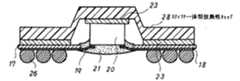
図1は、本発明の電子装置の第1の実施例の要部を断面的に示したものであり、 Tape-BGA型の半導体パッケージをマザーボードに搭載したものである。
【0032】
図において、符号17は、デバイスホール17aを有するポリイミド樹脂フィルムのような絶縁樹脂フィルムを示し、この絶縁樹脂フィルム17の一方の主面(図では下面)には、信号線等の配線18と、後端部が信号線等の配線18に接続され先端部がデバイスホール17aに突出したインナーリード19が、それぞれ配設されている。また、信号線等の配線18の他端部には、外部接続端子である接続パッド(図示を省略。)が、格子状のパターンで配設されている。また、このような配線フィルムのデバイスホール17a内には、半導体素子20がフェースダウンに配置されており、この半導体素子20の各電極端子(図示を省略。)は、対応するインナーリード19の先端部に、金バンプ20a等を介して電気的に接続されている。さらに、このような半導体素子20の電極端子とインナーリード19との接合部の外側には、半導体素子の保護および補強のために、エポキシ樹脂等の樹脂封止層21が被覆されている。
【0033】
また、絶縁樹脂フィルム17の配線形成面と反対側の面(図では上面)のデバイスホール17aを囲む領域には、SUS310 S(熱膨脹率15.9×10⁻⁶/K)やCDAAlloy C15150(熱膨脹率16.7×10⁻⁶/K)のような、13×10-6〜17×10-6/Kの熱膨脹率を有する金属から構成された枠形の形状保持板(スティフナー)22が、熱可塑性のポリエステル系樹脂のような熱可塑性樹脂から成る接着剤層23を介して接着されており、さらにこのスティフナー22の上面および半導体素子20の上面(電極端子形成面と反対側の面)には、銅、アルミニウム等の放熱性を有する金属からなる板状のカバー(カバープレート)24が配設され、熱可塑性ポリエステル系樹脂等から成る接着剤層25を介して接着されている。なお、カバープレート24は、半導体素子20の上面には全面的に接着されているが、スティフナー22の上面には、下側に突出形成された凹部24aのみが接着されている。
【0034】
さらに、配線フィルムの外部接続端子(接続パッド)上には、それぞれボール状のはんだバンプ26が設けられ、半導体パッケージが構成されている。
【0035】
一方、符号27は、マザーボードであるガラスエポキシ配線基板を示し、その一方の主面(図では上面)には、配線の一部として接続パッド(図示を省略。)が配設されている。そして、このガラスエポキシ配線基板27上に前記した半導体パッケージが搭載され、半導体パッケージの外部接続端子(接続パッド)とガラスエポキシ配線基板27の接続パッドとが、はんだバンプ26により電気的・機械的に接続されている。
【0036】
このように構成される第1の実施例の電子装置においては、スティフナー22が、SUS310 SやCDAAlloy C15150のような13×10-6〜17×10-6/Kの熱膨脹率を有する金属から構成されており、半導体パッケージ全体の熱膨脹率が、マザーボードであるガラスエポキシ配線基板27の熱膨脹率と近似した値となっているので、周期的な熱負荷が加えられたときに、半導体パッケージとマザーボードとを接続するはんだバンプ26の歪みが 3%以下と小さく、接続部が高い信頼性を有する。
【0037】
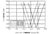
次に、具体的な効果をより明らかにするために、図1に示す構造の電子装置において、スティフナーを熱膨脹率の異なる種々の金属により構成した構造をシミュレーションし、温度サイクル試験( -65℃〜 120℃)を行なった。すなわち、スティフナーの厚さを 250μm 、接着剤層の厚さを 100μm とし、スティフナーを構成する金属材料の熱膨脹率を変えた半導体パッケージ(パッケージサイズ35mm×35mm)を、13×10-6 /K(13ppm/K)、15ppm/Kおよび18ppm/Kの熱膨脹率を有するガラスエポキシ配線基板上にそれぞれ搭載・実装した電子装置において、 -65℃×30分次いで 120℃×30分の温度サイクルを繰り返した後のはんだバンプの変形量を、シミュレーションにより求めた。結果を図2に示す。
【0038】
この結果から、スティフナをSUS310 SやCDAAlloy C15150のような熱膨脹率が13〜17ppm/Kの金属により構成した実施例の電子装置では、マザーボードであるガラスエポキシ配線基板の熱膨脹率が、13ppm/K、15ppm/Kあるいは18ppm/Kのいずれであっても、17ppm/K以上の熱膨脹率を有する金属(SUS304)によりスティフナーが構成された従来の電子装置に比べて、はんだバンプの変形量が著しく小さくなっていることがわかる。したがって、実施例の電子装置は、従来の電子装置に比べて、数倍から10数倍の回数の温度サイクルに耐え得ることがわかる。
【0039】
実際に、スティフナーの構成材料としてCDAAlloy C15150を使用し、図1に示す電子装置を作製して温度サイクル試験( -65℃〜 120℃)を行なったところ、1000サイクルを越えた時点でも、はんだバンプに疲労破壊の発生が認められず、信頼性の高い接続が保持されていることが確認された。
【0040】
また、第1の実施例に使用した半導体パッケージにおいては、スティフナーを構成する剛性材料として金属が使用されているが、金属は、他の剛性材料(例えばセラミック)に比べて、高い熱伝導率を有し、放熱性が良好であるうえに、成形・加工性が良好で曲げ加工や切断加工が容易であり、さらに平坦性が良く、反り等が生じても元の平坦面に戻しやすいという種々の利点を有している。したがって、平坦性が良好なスティフナーを容易に成形することができ、放熱性の良好な半導体パッケージを得ることができる。
【0041】
スティフナーを構成する剛性材料として、金属(例えば、CDAAlloy C15150)とセラミック(例えば、アルミナ)とをそれぞれ選択し、それらの特性を比較したものを、以下の表1に示す。
【0042】
【表1】
【0043】
図3は、本発明の第2の実施例に係る半導体パッケージの要部を断面的に示したものである。なお、図3において、図1と同一の部分には同一の符号を付して、説明を省略する。
【0044】
この実施例の半導体パッケージでは、半導体素子20および絶縁フィルム17の上側に、形状保持性を有する放熱キャップ(スティフナ一体型放熱キャップ)28が配置され、この放熱キャップ28が、熱可塑性ポリエステル系樹脂等から成る接着剤層23を介して、半導体素子20の上面および絶縁フィルム17の上面に接着されている。そして、このスティフナ一体型放熱キャップ28が、SUS310 SやCDAAlloy C15150のような、13×10-6〜17×10-6/Kの熱膨脹率を有する金属により構成されている。
【0045】
この実施例の半導体パッケージにおいても、これをガラスエポキシ配線基板27上に搭載し、はんだバンプ26を介して所要の接続を行なうことで、信頼性の高い接続が得られる。すなわち、第2の実施例の半導体パッケージの外部接続端子(接続パッド)と、マザーボードであるガラスエポキシ配線基板27の接続パッドとを、はんだバンプ26により電気的・機械的に接続した電子装置では、熱サイクル時にはんだバンプ26に応力集中による歪みが生じにくく、信頼性の高い接続が保持される。
【0046】
また、第2の実施例の半導体パッケージでは、スティフナーと放熱性のカバープレートとが重ねて配置される代わりに、これらの機能を併せ持ったスティフナ一体型放熱キャップ28が配設され、かつこれがSUS310 SやCDAAlloy C15150のような金属から構成されているので、半導体パッケージおよびパッケージが搭載された電子装置全体を薄くすることが可能であるうえに、放熱キャップの成形が容易であり、製造工程が簡略化される。また、部品点数が少なくて済む。さらに、スティフナ一体型放熱キャップ28と絶縁フィルム17との接着面積が大きく、放熱経路の断面積が大きくなっているので、放熱性が良好である。
【0047】
なお、本発明は、前記した第1および第2の実施例の半導体パッケージおよび電子装置に限定されるものではなく、発明の趣旨を逸脱しない範囲でいろいろに変形させることができる。例えばマザーボードとして、ガラスエポキシ配線基板以外に、ガラスポリイミド配線基板やガラスBT樹脂配線基板のようなガラス樹脂配線基板、あるいはアルミナや窒化アルミニウムのようなセラミックを絶縁基材とするセラミック配線基板を使用することができる。
【0048】
【発明の効果】
以上の説明から明らかなように、本発明の電子装置によれば、形状保持板または形状保持性を有する被覆部材の構成材料として、マザーボードと近似した熱膨脹率を有する金属が使用されており、半導体パッケージ全体の熱膨脹率がマザーボードの熱膨脹率とほぼ等しくなっているので、実際の使用環境等において、周期的に印加される熱的な負荷に起因して接続部に生じる応力を緩和することができる。したがって、半導体パッケージとマザーボードとの接続の信頼性が向上される。
【0049】
また、本発明の半導体パッケージによれば、これをマザーボードに搭載した場合に、形状保持板または形状保持性を有する被覆部材の熱膨張率とマザーボードの熱膨張率との差に起因して生じる応力を緩和することができるので、接続部であるはんだボール等のバンプの歪み等が抑制され、疲労破壊が生じにくくなる。したがって、電子装置の接続信頼性を大きく向上させることができる。
【図面の簡単な説明】
【図1】本発明の第1の実施例に係る電子装置の要部の構成を示す断面図。
【図2】図1に示す電子装置において、スティフナーを熱膨脹率の異なる金属により構成して、シミュレーションにより温度サイクル試験を行なった結果を示すグラフ。
【図3】本発明の第2の実施例に係る半導体パッケージの要部の構成を示す断面図。
【図4】従来からの Tape-BGA型半導体パッケージの構成を示す斜視図。
【図5】QFPをマザーボードに実装した電子装置の断面図。
【符号の説明】
17………絶縁樹脂フィルム
17a………デバイスホール
19………インナーリード
20………半導体素子
21………樹脂封止層
22………スティフナー
23………接着剤層
24………カバープレート
26………はんだバンプ
27………ガラスエポキシ配線基板
28………スティフナ一体型放熱キャップ[0001]
BACKGROUND OF THE INVENTION
The present invention relates to an electronic device and a semiconductor package. More specifically, the present invention relates to a highly reliable electronic device in which a semiconductor package is mounted on a wiring board that is a mother board, and high reliability when mounted on a wiring board that is a mother board. The present invention relates to a semiconductor package having a structure.
[0002]
[Prior art]
For the purpose of downsizing electronic devices and circuit structures, mounting and mounting semiconductor elements (for example, IC chips) on multilayer wiring boards such as ceramics, and sealing the mounting area with metal caps Alternatively, semiconductor devices coated or sealed with a mold resin have been widely put into practical use.
[0003]
In particular, a semiconductor device with high power consumption, such as a CPU, has a configuration in which a heat radiating body (heat sink) is attached to release heat generated during operation from the heat radiating body.
[0004]
Furthermore, for the purpose of reducing costs and simplifying the configuration, a semiconductor element is mounted and mounted on a carrier tape having wiring such as an inner lead, and a shape retaining plate called a stiffener is attached, and further a heat-radiating cover Also known is a TCP (tape carrier package) comprising: In such a TCP, from the viewpoint of increase in the number of input / output terminals, downsizing of the outer shape, ease of mounting, etc., solder balls or the like are formed on connection pads that are terminals for connection to external circuits (external connection terminals). A structure called a ball grid array (hereinafter referred to as BGA) is adopted in which bumps are arranged and these bumps are arranged in a lattice pattern.
[0005]
FIG. 4 is a perspective view showing an example of the structure of such a Tape-BGA type semiconductor package. In the figure,
[0006]
Such a semiconductor package is mounted and mounted on a wiring board (motherboard) on the host side to constitute an electronic device. That is, on one main surface of the motherboard, connection pads are arranged corresponding to the external connection terminals (connection pads) of the semiconductor package, and the connection pads of the motherboard and the external connection terminals of the semiconductor package are solder balls. Connected by bumps such as 5.
[0007]
[Problems to be solved by the invention]
However, in an electronic device mounted with a semiconductor package in this way, stress caused by a thermal load applied during mounting or in an actual use environment causes the external connection terminal of the semiconductor package and the connection pad of the motherboard to There is a problem that the
[0008]
That is, as a motherboard, a glass epoxy wiring board in which a glass cloth-epoxy resin impregnated layer and a copper wiring layer are laminated is usually used. The thermal expansion rate (linear expansion rate) of this wiring board is the wiring density or wiring. 13 × 10 on average, depending on direction-6~ 18 × 10-6/ C (/ K) range.
[0009]
On the other hand, in the semiconductor package shown in FIG. 4, the stiffener 6 which occupies the largest proportion in terms of thickness and thus determines the thermal expansion coefficient of the entire package is 17 × 10 6.-6(/ K) stainless steel having a large thermal expansion coefficient (for example, SUS304; thermal expansion coefficient 17.3 × 10⁻⁶), There is a thermal property mismatch between the semiconductor package and the motherboard.
[0010]
When the physical properties are greatly different in this way, in the QFP (Quad Flat Package), the outer lead portion formed into a gull wing shape is elastically deformed to absorb and relieve strain due to stress concentration. In the BGA type semiconductor package, since there is no part that absorbs and relaxes such strain, cyclic stress changes, and the stress acts repeatedly on the bumps of the
[0011]
An electronic device in which QFP is mounted on a glass epoxy wiring board and mounted is shown in FIG. In this figure,
[0012]
The present invention has been made to solve such a problem, and an object of the present invention is to provide an electronic device with high reliability of a connection portion between a semiconductor package and a mother board. It is another object of the present invention to provide a semiconductor package capable of obtaining a highly reliable electronic device by mounting on a mother board.
[0013]
[Means for Solving the Problems]
The electronic device of the first invention of the present invention isA wiring board having connection terminals disposed on one main surface, a wiring film having a device hole, and having an external connection terminal and an inner lead protruding from the device hole on one main surface, and the wiring film A semiconductor element disposed in the device hole and electrically connected to the inner lead, and a metal having a thermal expansion coefficient substantially equal to a thermal expansion coefficient of the wiring board, and the other main surface of the wiring film And a bump that electrically and mechanically connects an external connection terminal of the semiconductor package and a connection terminal of the wiring board. An electronic device comprising: the shape retaining plate,twenty fiveCr-20Ni stainless steel, or0.01~0.03By copper alloy containing Zr in weight%It is configured.
[0014]
Here, the bump for electrically and mechanically connecting the external connection terminal of the semiconductor package and the connection terminal of the wiring board as the motherboard can be a ball-shaped bump made of solder such as Pb-Sn. The formation of the solder bump is performed, for example, by placing a pre-shaped solder ball on a connection pad that is an external connection terminal of the wiring film and heating (melting) the solder by heating.
[0015]
In addition, a heat-dissipating coating member can be disposed outside the semiconductor element of the semiconductor package. As a covering member having heat dissipation, for example, a plate made of a metal having high thermal conductivity such as copper or aluminum, a plate made of ceramic such as alumina (aluminum oxide) or aluminum nitride, or a plurality of these plate materials The thing of the structure which has arrange | positioned the sheet | seat laminated | stacked is used. The thickness, shape, and the like of the covering member are appropriately selected in consideration of the capacity of the semiconductor element and heat release properties.
[0016]
Further, as the wiring board, a glass epoxy wiring board having a structure in which a glass cloth-epoxy resin impregnated layer and a copper wiring layer are laminated and integrated is used, and the shape retention plate is used as a thermal expansion coefficient (13 × 10 6) of the glass epoxy wiring board.-6~ 18 × 10-6/ K), approximately equal to 13 × 10-6~ 17 × 10-6It can be composed of a metal having a coefficient of thermal expansion of / K. And 13 × 10-6~ 17 × 10-6As a metal having a thermal expansion coefficient of / K, 25Cr-20Ni stainless steel (for example, SUS310 S; thermal expansion coefficient 15.9 × 10⁻⁶/ K), or a copper alloy containing 0.01 to 0.03% by weight of Zr (eg CDA Alloy C15150; coefficient of thermal expansion 16.7 × 10⁻⁶/ K) can be used. In particular, CDAAlloy C15150 has a very high thermal conductivity of 15 to 20 W · m / K and is excellent in heat dissipation, and is therefore suitable as a constituent material for the shape holding plate. SUS310 S is easy to obtain, is relatively inexpensive, and has good corrosion resistance.
[0017]
The electronic device of the second invention of the present invention isA wiring board having connection terminals disposed on one main surface, a wiring film having a device hole, and having an external connection terminal and an inner lead protruding from the device hole on one main surface, and the wiring film A semiconductor element disposed in the device hole and electrically connected to the inner lead, and a metal having a thermal expansion coefficient substantially equal to the thermal expansion coefficient of the wiring board, and covers the outside of the semiconductor element. And a semiconductor package having a shape-retaining covering member bonded to the other main surface of the wiring film, an external connection terminal of the semiconductor package, and a connection terminal of the wiring board. An electronic device including a bump connected to the covering member having the shape retaining property described above,twenty fiveCr-20Ni stainless steel, or0.01~0.03By copper alloy containing Zr in weight%It is configured.
[0018]
Here, the bump for electrically and mechanically connecting the external connection terminal of the semiconductor package and the connection terminal of the wiring board as the motherboard can be a ball-shaped bump made of solder such as Pb-Sn.
[0019]
In addition, the above-described glass epoxy wiring board is used as the wiring board, and the covering member having shape retaining property is approximately equal to the thermal expansion coefficient of the glass epoxy wiring board, 13 × 10.-6~ 17 × 10-6It can be composed of a metal having a coefficient of thermal expansion of / K. As a metal having a thermal expansion coefficient in such a range, for example, 25Cr-20Ni stainless steel such as SUS310 S or a copper alloy such as CDAAlloy C15150 can be used.
[0020]
Furthermore, the semiconductor package of the third invention of the present invention has a device hole, a wiring film in which an external connection terminal and an inner lead protruding into the device hole are arranged on one main surface, and the wiring film A semiconductor element disposed in the device hole and electrically connected to the inner lead;13×Ten-6~17×Ten-6(/ K) composed of a metal having a coefficient of thermal expansion,A frame-shaped shape holding plate disposed in a region surrounding the device hole on the other main surface of the wiring film.Semiconductor packageThe shape retaining plate istwenty fiveCr-20Ni stainless steel, or0.01~0.03By copper alloy containing Zr in weight%It is configured.
[0021]
According to a fourth aspect of the present invention, there is provided a semiconductor package having a device hole, a wiring film having an external connection terminal and an inner lead projecting from the device hole on one main surface, and the wiring film A semiconductor element disposed in the device hole and electrically connected to the inner lead;13×Ten-6~17×Ten-6(/ K) made of a metal having a coefficient of thermal expansion,Arranged to cover the outside of the semiconductor elementAndAnd a covering member having a shape retaining property adhered to the other main surface of the wiring film.Semiconductor packageThe covering member having the shape retaining property described above istwenty fiveCr-20Ni stainless steel, or0.01~0.03By copper alloy containing Zr in weight%It is configured.
[0022]
Here, 13 × 10 constituting the shape-retaining plate or the covering member having shape-retaining properties-6~ 17 × 10-6As the metal having a thermal expansion coefficient of (/ K), for example, a 25Cr-20Ni stainless steel such as SUS310 S or a copper alloy such as CDAAlloy C15150 can be used.
[0023]
Also, a ball-shaped bump made of Pb—Sn solder or the like is disposed on the external connection terminal, and an electrical / mechanical connection with the connection terminal of the motherboard is performed via the solder bump. can do.
[0024]
In the semiconductor package and the electronic device of the present invention, an insulating resin film such as a polyimide resin film can be used as the substrate of the wiring film having device holes. The thickness of the insulating resin film is preferably about 50 to 125 μm, although it depends on the type, shape, size, etc. of the semiconductor package. The size and planar shape of the device hole are set corresponding to the planar size and shape of the semiconductor element to be mounted / mounted.
[0025]
On one main surface of such an insulating resin film, wiring such as a signal line and inner leads having one end protruding into the device hole and the other end connected to the signal line or the like are disposed. In addition, connection pads that are external connection terminals are disposed at the ends of the wiring. Such wiring including the inner lead is composed of Cu, Cu alloy, Ni alloy such as 42 alloy, etc., and is provided on one side of the insulating resin film by vapor deposition patterning on the insulating resin film. It is formed by photo-patterning the Cu foil or the alloy layer. The pitch and arrangement of the inner leads are set corresponding to the pitch and arrangement of the electrode terminals of the semiconductor element to be mounted / mounted.
[0026]
The semiconductor elements mounted and mounted on such a wiring film are elements such as a CPU, a DSP, and various memories, and are not particularly limited to chip-type elements. Such a semiconductor element is disposed in a device hole face down, and is electrically connected by bonding an electrode terminal made of Al or the like to the tip of the corresponding inner lead via a gold bump or the like. The In addition, in order to protect the semiconductor element against moisture or impurities in the outside world or mechanically, the connection region of such a semiconductor element can be covered and sealed with a resin layer. Here, as the resin, a resin usually used for sealing a semiconductor element, such as an epoxy resin or a sulfonic acid resin, can be used.
[0027]
In the electronic device of the present invention, the shape retaining plate or the shape retaining covering member provided in the semiconductor package is made of a metal having a thermal expansion coefficient similar to that of the mother board, and the thermal expansion coefficient of the entire package is that of the mother board. Since it is almost equal to the thermal expansion coefficient, stress is concentrated on bumps such as solder balls, which are the joints between the semiconductor package and the motherboard, when a periodic temperature change is applied during mounting or usage. There is no. Therefore, the occurrence of distortion and fatigue failure due to the thermal load is suppressed, and the reliability of the connection between the semiconductor package and the mother board is improved.
[0028]
In addition, the metal that forms the shape-retaining plate or the covering member having shape-retaining properties has higher thermal conductivity and better heat dissipation than other rigid materials such as ceramics. It has many advantages such as good workability, good flatness, and easy return to the original flat surface even if warpage occurs. Furthermore, since the material selectivity is good, a material having a thermal expansion coefficient as close as possible to that of the motherboard can be selected and used from various metal materials. An electronic device that is suitable and excellent in characteristics can be obtained with high productivity.
[0029]
Furthermore, in a semiconductor package provided with a covering member having shape retention and an electronic device equipped with this semiconductor package, the package and the entire device can be made thin, and the number of components can be reduced. it can. The covering member having a cap shape or the like can be formed only by using a metal, and can be easily formed by a simplified process.
[0030]
DETAILED DESCRIPTION OF THE INVENTION
Embodiments of the present invention will be described below with reference to the drawings.
[0031]
FIG. 1 is a cross-sectional view of a main part of a first embodiment of an electronic device according to the present invention, in which a tape-BGA type semiconductor package is mounted on a mother board.
[0032]
In the figure,
[0033]
Further, in the region surrounding the device hole 17a on the surface opposite to the wiring forming surface of the insulating resin film 17 (upper surface in the figure), SUS310 S (thermal expansion coefficient 15.9 × 10⁻⁶/ K) and CDAAlloy C15150 (thermal expansion coefficient 16.7 × 10⁻⁶/ K), 13 × 10-6~ 17 × 10-6A frame-shaped shape holding plate (stiffener) 22 made of a metal having a thermal expansion coefficient of / K is bonded via an
[0034]
Furthermore, ball-shaped solder bumps 26 are provided on the external connection terminals (connection pads) of the wiring film to constitute a semiconductor package.
[0035]
On the other hand,
[0036]
In the electronic apparatus of the first embodiment constructed as described above, the stiffener 22 is 13 × 10 6 such as SUS310 S or CDA Alloy C15150.-6~ 17 × 10-6Since the thermal expansion coefficient of the entire semiconductor package is a value that approximates the thermal expansion coefficient of the glass
[0037]
Next, in order to clarify the specific effect, in the electronic device having the structure shown in FIG. 1, a structure in which the stiffener is made of various metals having different coefficients of thermal expansion is simulated, and a temperature cycle test (from −65 ° C. to 120 ° C.). In other words, a semiconductor package (package size 35 mm x 35 mm) with a stiffener thickness of 250 μm and an adhesive layer thickness of 100 μm and varying the coefficient of thermal expansion of the metal material constituting the stiffener is 13 x 10-6 -65 ° C x 30 minutes, then 120 ° C x 30 minutes temperature cycle in electronic devices mounted and mounted on glass epoxy wiring boards with thermal expansion rates of 15K / K (13ppm / K), 15ppm / K and 18ppm / K, respectively The deformation amount of the solder bump after repeating the above was obtained by simulation. The results are shown in FIG.
[0038]
From this result, in the electronic device of the example in which the stiffener is made of a metal having a thermal expansion coefficient of 13 to 17 ppm / K, such as SUS310 S or CDA Alloy C15150, the thermal expansion coefficient of the glass epoxy wiring board as the motherboard is 13 ppm / K, At 15 ppm / K or 18 ppm / K, the amount of solder bump deformation is significantly smaller than conventional electronic devices that have a stiffener made of metal (SUS304) with a coefficient of thermal expansion of 17 ppm / K or higher. You can see that Therefore, it can be seen that the electronic device of the example can withstand a temperature cycle several times to 10 times as many times as the conventional electronic device.
[0039]
Actually, CDAAlloy C15150 was used as a stiffener component, and the electronic device shown in FIG. 1 was manufactured and subjected to a temperature cycle test (-65 ° C. to 120 ° C.). No fatigue failure was observed, and it was confirmed that a highly reliable connection was maintained.
[0040]
In the semiconductor package used in the first embodiment, a metal is used as a rigid material constituting the stiffener. However, the metal has a higher thermal conductivity than other rigid materials (for example, ceramic). In addition to having good heat dissipation, forming and workability are good, bending and cutting are easy, flatness is good, and it is easy to return to the original flat surface even if warpage occurs. Has the advantage of Therefore, a stiffener with good flatness can be easily formed, and a semiconductor package with good heat dissipation can be obtained.
[0041]
Table 1 below shows a comparison of the properties of metals (for example, CDA Alloy C15150) and ceramics (for example, alumina) selected as the rigid material constituting the stiffener.
[0042]
[Table 1]
[0043]
FIG. 3 is a sectional view showing a main part of a semiconductor package according to the second embodiment of the present invention. In FIG. 3, the same parts as those in FIG.
[0044]
In the semiconductor package of this embodiment, a heat dissipating cap (stiffener integrated heat dissipating cap) 28 having shape retaining property is disposed above the
[0045]
Also in the semiconductor package of this embodiment, a highly reliable connection can be obtained by mounting it on the glass
[0046]
In the semiconductor package of the second embodiment, instead of the stiffener and the heat-dissipating cover plate being stacked, a stiffener-integrated heat dissipating cap 28 having these functions is provided, and this is made of SUS310 S And CDAAlloy C15150, it is possible to reduce the thickness of the entire semiconductor package and the electronic device on which the package is mounted, and the heat dissipation cap can be easily molded, thus simplifying the manufacturing process. Is done. Also, the number of parts can be reduced. Furthermore, since the bonding area between the stiffener integrated heat dissipation cap 28 and the insulating
[0047]
The present invention is not limited to the semiconductor packages and electronic devices of the first and second embodiments described above, and can be variously modified without departing from the spirit of the invention. For example, as the motherboard, in addition to the glass epoxy wiring board, a glass resin wiring board such as a glass polyimide wiring board or a glass BT resin wiring board, or a ceramic wiring board using a ceramic such as alumina or aluminum nitride as an insulating base is used. be able to.
[0048]
【The invention's effect】
As is clear from the above description, according to the electronic device of the present invention, a metal having a thermal expansion coefficient similar to that of a mother board is used as a constituent material of a shape-retaining plate or a covering member having shape-retaining properties. Since the thermal expansion coefficient of the entire package is almost equal to the thermal expansion coefficient of the motherboard, it is possible to relieve the stress generated in the connection portion due to a periodically applied thermal load in an actual use environment or the like. . Therefore, the reliability of the connection between the semiconductor package and the mother board is improved.
[0049]
Further, according to the semiconductor package of the present invention, when this is mounted on a mother board, the stress caused by the difference between the thermal expansion coefficient of the shape retaining plate or the covering member having shape retainability and the thermal expansion coefficient of the mother board. Therefore, distortion of bumps such as solder balls as connection portions is suppressed, and fatigue failure is less likely to occur. Therefore, the connection reliability of the electronic device can be greatly improved.
[Brief description of the drawings]
FIG. 1 is a cross-sectional view showing a configuration of a main part of an electronic device according to a first embodiment of the invention.
2 is a graph showing a result of a temperature cycle test performed by simulation in the electronic device shown in FIG. 1 in which stiffeners are made of metals having different thermal expansion coefficients.
FIG. 3 is a cross-sectional view showing a configuration of a main part of a semiconductor package according to a second embodiment of the present invention.
FIG. 4 is a perspective view showing a configuration of a conventional Tape-BGA type semiconductor package.
FIG. 5 is a cross-sectional view of an electronic device in which QFP is mounted on a motherboard.
[Explanation of symbols]
17 ……… Insulating resin film
17a ... Device Hall
19 ……… Inner Lead
20 ......... Semiconductor element
21 ... …… Resin sealing layer
22 ……… Stiffener
23 .... Adhesive layer
24 ... …… Cover plate
26 ………… Solder bump
27 ………… Glass epoxy wiring board
28 ......... Stiffener integrated heat dissipation cap
Claims (6)
Translated fromJapaneseデバイスホールを有し、一主面に外部接続端子および前記デバイスホールに突出したインナーリードがそれぞれ配設された配線フィルムと、この配線フィルムの前記デバイスホール内に配置され、前記インナーリードに電気的に接続された半導体素子と、前記配線基板の熱膨脹率とほぼ等しい熱膨脹率を有する金属により構成されており、前記配線フィルムの他主面の前記デバイスホールを囲む領域に配設された枠形の形状保持板とを有する半導体パッケージと、
前記半導体パッケージの外部接続端子と前記配線基板の接続端子とを電気的・機械的に接続するバンプとを備えた電子装置であって、
前記形状保持板が、25Cr−20Niステンレス鋼、または0.01〜0.03重量%のZrを含む銅合金により構成されていることを特徴とする電子装置。A wiring board having connection terminals on one main surface;
A wiring film having a device hole and having an external connection terminal and an inner lead protruding into the device hole on one main surface, and the wiring film disposed in the device hole of the wiring film, electrically connected to the inner lead And a metal element having a thermal expansion coefficient substantially equal to the thermal expansion coefficient of the wiring board, and a frame-shaped element disposed in a region surrounding the device hole on the other main surface of the wiring film. A semiconductor package having a shape retaining plate;
An electronic device comprising a bump for electrically and mechanically connecting an external connection terminal of the semiconductor package and a connection terminal of the wiring board,
An electronic device, wherein the shape retaining plate is made of 25Cr-20Ni stainless steel or a copper alloy containing 0.01 to 0.03% by weight of Zr.
デバイスホールを有し、一主面に外部接続端子および前記デバイスホールに突出したインナーリードがそれぞれ配設された配線フィルムと、この配線フィルムの前記デバイスホール内に配置され、前記インナーリードに電気的に接続された半導体素子と、前記配線基板の熱膨脹率とほぼ等しい熱膨脹率を有する金属により構成されており、前記半導体素子の外側を覆って配置されかつ前記配線フィルムの他主面に接着された形状保持性を有する被覆部材とを有する半導体パッケージと、
前記半導体パッケージの外部接続端子と前記配線基板の接続端子とを電気的・機械的に接続するバンプとを備えた電子装置であって、
前記した形状保持性を有する被覆部材が、25Cr−20Niステンレス鋼、または0.01〜0.03重量%のZrを含む銅合金により構成されていることを特徴とする電子装置。A wiring board having connection terminals on one main surface;
A wiring film having a device hole and having an external connection terminal and an inner lead protruding into the device hole on one main surface, and the wiring film disposed in the device hole of the wiring film, electrically connected to the inner lead And a metal having a thermal expansion coefficient substantially equal to the thermal expansion coefficient of the wiring board, arranged to cover the outside of the semiconductor element and bonded to the other main surface of the wiring film A semiconductor package having a covering member having shape retention;
An electronic device comprising a bump for electrically and mechanically connecting an external connection terminal of the semiconductor package and a connection terminal of the wiring board,
An electronic device, wherein the covering member having shape retention described above is made of 25Cr-20Ni stainless steel or a copper alloy containing 0.01 to 0.03% by weight of Zr.
前記形状保持板が、25Cr−20Niステンレス鋼、または0.01〜0.03重量%のZrを含む銅合金により構成されていることを特徴とする半導体パッケージ。A wiring film having a device hole and having an external connection terminal and an inner lead protruding into the device hole on one main surface, and the wiring film disposed in the device hole of the wiring film, electrically connected to the inner lead And a metal element having a thermal expansion coefficient of 13 × 10−6 to 17 × 10−6 (/ K) and disposed in a region surrounding the device hole on the other main surface of the wiring film. A semiconductor package having a frame-shaped shape holding plate,
A semiconductor package, wherein the shape retaining plate is made of 25Cr-20Ni stainless steel or a copper alloy containing 0.01 to 0.03% by weight of Zr.
前記した形状保持性を有する被覆部材が、25Cr−20Niステンレス鋼、または0.01〜0.03重量%のZrを含む銅合金により構成されていることを特徴とする半導体パッケージ。A wiring film having a device hole and having an external connection terminal and an inner lead protruding into the device hole on one main surface, and the wiring film disposed in the device hole of the wiring film, electrically connected to the inner lead And a metal element having a coefficient of thermal expansion of 13 × 10−6 to 17 × 10−6 (/ K), disposed outside the semiconductor element, and formed of the wiring film. It is a semiconductor package provided with a covering member having a shape retaining property bonded to another main surface,
A semiconductor package characterized in that the covering member having the shape retaining property described above is made of 25Cr-20Ni stainless steel or a copper alloy containing 0.01 to 0.03% by weight of Zr.
Priority Applications (4)
| Application Number | Priority Date | Filing Date | Title |
|---|---|---|---|
| JP20400298AJP3724954B2 (en) | 1997-08-29 | 1998-07-17 | Electronic device and semiconductor package |
| TW087113727ATW466718B (en) | 1997-08-29 | 1998-08-20 | Electronic device and semiconductor package |
| US09/140,541US6097085A (en) | 1997-08-29 | 1998-08-26 | Electronic device and semiconductor package |
| KR1019980034779AKR100308137B1 (en) | 1997-08-29 | 1998-08-27 | Electronics and Semiconductor Packages |
Applications Claiming Priority (3)
| Application Number | Priority Date | Filing Date | Title |
|---|---|---|---|
| JP9-233695 | 1997-08-29 | ||
| JP23369597 | 1997-08-29 | ||
| JP20400298AJP3724954B2 (en) | 1997-08-29 | 1998-07-17 | Electronic device and semiconductor package |
Publications (3)
| Publication Number | Publication Date |
|---|---|
| JPH11135679A JPH11135679A (en) | 1999-05-21 |
| JPH11135679A5 JPH11135679A5 (en) | 2005-04-07 |
| JP3724954B2true JP3724954B2 (en) | 2005-12-07 |
Family
ID=26514231
Family Applications (1)
| Application Number | Title | Priority Date | Filing Date |
|---|---|---|---|
| JP20400298AExpired - Fee RelatedJP3724954B2 (en) | 1997-08-29 | 1998-07-17 | Electronic device and semiconductor package |
Country Status (4)
| Country | Link |
|---|---|
| US (1) | US6097085A (en) |
| JP (1) | JP3724954B2 (en) |
| KR (1) | KR100308137B1 (en) |
| TW (1) | TW466718B (en) |
Families Citing this family (18)
| Publication number | Priority date | Publication date | Assignee | Title |
|---|---|---|---|---|
| US5719440A (en) | 1995-12-19 | 1998-02-17 | Micron Technology, Inc. | Flip chip adaptor package for bare die |
| US6861290B1 (en) | 1995-12-19 | 2005-03-01 | Micron Technology, Inc. | Flip-chip adaptor package for bare die |
| USRE43112E1 (en) | 1998-05-04 | 2012-01-17 | Round Rock Research, Llc | Stackable ball grid array package |
| US6117797A (en)* | 1998-09-03 | 2000-09-12 | Micron Technology, Inc. | Attachment method for heat sinks and devices involving removal of misplaced encapsulant |
| US6198166B1 (en)* | 1999-07-01 | 2001-03-06 | Intersil Corporation | Power semiconductor mounting package containing ball grid array |
| KR100377471B1 (en)* | 1999-12-10 | 2003-03-26 | 앰코 테크놀로지 코리아 주식회사 | semiconductor package and its manufacturing method |
| JP2002057252A (en)* | 2000-08-07 | 2002-02-22 | Hitachi Ltd | Semiconductor device and manufacturing method thereof |
| KR100680731B1 (en)* | 2000-09-01 | 2007-02-09 | 삼성전자주식회사 | Semiconductor Package and Manufacturing Method |
| JP2002270717A (en)* | 2001-03-12 | 2002-09-20 | Rohm Co Ltd | Semiconductor device |
| US20030218246A1 (en)* | 2002-05-22 | 2003-11-27 | Hirofumi Abe | Semiconductor device passing large electric current |
| JP4143609B2 (en)* | 2003-05-23 | 2008-09-03 | 富士通株式会社 | Wiring board manufacturing method |
| TWI246760B (en)* | 2004-12-22 | 2006-01-01 | Siliconware Precision Industries Co Ltd | Heat dissipating semiconductor package and fabrication method thereof |
| US7851904B2 (en)* | 2006-12-06 | 2010-12-14 | Panasonic Corporation | Semiconductor device, method for manufacturing the same, and semiconductor device mounting structure |
| DE102008006390A1 (en)* | 2008-01-28 | 2009-07-30 | Tesa Ag | Method for bonding flexible printed circuit boards with polymer materials for partial or complete stiffening |
| US8804339B2 (en) | 2011-02-28 | 2014-08-12 | Toyota Motor Engineering & Manufacturing North America, Inc. | Power electronics assemblies, insulated metal substrate assemblies, and vehicles incorporating the same |
| CN102790034A (en)* | 2011-05-17 | 2012-11-21 | 飞思卡尔半导体公司 | Semiconductor apparatus with radiator |
| KR101432486B1 (en)* | 2012-10-08 | 2014-08-21 | 에스티에스반도체통신 주식회사 | Method for manufacturing of integrated circuit package |
| US20210043466A1 (en)* | 2019-08-06 | 2021-02-11 | Texas Instruments Incorporated | Universal semiconductor package molds |
Family Cites Families (6)
| Publication number | Priority date | Publication date | Assignee | Title |
|---|---|---|---|---|
| JPH08213497A (en)* | 1995-02-03 | 1996-08-20 | Fujitsu Ltd | Semiconductor device and manufacturing method thereof |
| SG45122A1 (en)* | 1995-10-28 | 1998-01-16 | Inst Of Microelectronics | Low cost and highly reliable chip-sized package |
| JPH09181209A (en)* | 1995-12-26 | 1997-07-11 | Hitachi Ltd | Semiconductor device and manufacturing method thereof |
| US5760465A (en)* | 1996-02-01 | 1998-06-02 | International Business Machines Corporation | Electronic package with strain relief means |
| US5900312A (en)* | 1996-11-08 | 1999-05-04 | W. L. Gore & Associates, Inc. | Integrated circuit chip package assembly |
| US5835355A (en)* | 1997-09-22 | 1998-11-10 | Lsi Logic Corporation | Tape ball grid array package with perforated metal stiffener |
- 1998
- 1998-07-17JPJP20400298Apatent/JP3724954B2/ennot_activeExpired - Fee Related
- 1998-08-20TWTW087113727Apatent/TW466718B/ennot_activeIP Right Cessation
- 1998-08-26USUS09/140,541patent/US6097085A/ennot_activeExpired - Fee Related
- 1998-08-27KRKR1019980034779Apatent/KR100308137B1/ennot_activeExpired - Fee Related
Also Published As
| Publication number | Publication date |
|---|---|
| KR100308137B1 (en) | 2001-12-17 |
| US6097085A (en) | 2000-08-01 |
| JPH11135679A (en) | 1999-05-21 |
| TW466718B (en) | 2001-12-01 |
| KR19990023924A (en) | 1999-03-25 |
Similar Documents
| Publication | Publication Date | Title |
|---|---|---|
| JP3724954B2 (en) | Electronic device and semiconductor package | |
| JP2881575B2 (en) | Ball grid array semiconductor package with heat sink | |
| KR100268205B1 (en) | Attaching heat sinks directly to flip chips and ceramic chip carriers | |
| JPH10163386A (en) | Semiconductor device, semiconductor package and mounting circuit device | |
| JP3134815B2 (en) | Semiconductor device | |
| JP2001520460A (en) | Method and structure for improving heat dissipation characteristics of package for microelectronic device | |
| JPH1117064A (en) | Semiconductor package | |
| JP2007158279A (en) | Semiconductor device and electronic control device using the same | |
| US6992380B2 (en) | Package for semiconductor device having a device-supporting polymeric material covering a solder ball array area | |
| JP3569585B2 (en) | Semiconductor device | |
| JP3339881B2 (en) | Semiconductor integrated circuit device and method of manufacturing the same | |
| JPH11220055A (en) | BGA type semiconductor device and stiffener used in the device | |
| JP2010219554A (en) | Semiconductor device and electronic controller using the same | |
| JPH10116936A (en) | Semiconductor package | |
| JPH09331004A (en) | Semiconductor device | |
| JP4130277B2 (en) | Semiconductor device and manufacturing method of semiconductor device | |
| JPH07111278A (en) | Resin sealed package and electronic circuit device | |
| US20240079366A1 (en) | Semiconductor package | |
| KR200292794Y1 (en) | Flexible Circuit Boards and Semiconductor Packages Using the Same | |
| KR19980025877A (en) | Ball grid array package with a heat sink attached to the chip | |
| JP2000058716A (en) | Semiconductor device | |
| JP4175339B2 (en) | Manufacturing method of semiconductor device | |
| TWM545363U (en) | Chip package structure | |
| TWI607540B (en) | Chip package structure and manufacturing method thereof | |
| JPS60200545A (en) | Mounting substrate |
Legal Events
| Date | Code | Title | Description |
|---|---|---|---|
| A521 | Written amendment | Free format text:JAPANESE INTERMEDIATE CODE: A523 Effective date:20040506 | |
| A621 | Written request for application examination | Free format text:JAPANESE INTERMEDIATE CODE: A621 Effective date:20040506 | |
| A977 | Report on retrieval | Free format text:JAPANESE INTERMEDIATE CODE: A971007 Effective date:20050909 | |
| TRDD | Decision of grant or rejection written | ||
| A01 | Written decision to grant a patent or to grant a registration (utility model) | Free format text:JAPANESE INTERMEDIATE CODE: A01 Effective date:20050913 | |
| A61 | First payment of annual fees (during grant procedure) | Free format text:JAPANESE INTERMEDIATE CODE: A61 Effective date:20050920 | |
| FPAY | Renewal fee payment (event date is renewal date of database) | Free format text:PAYMENT UNTIL: 20080930 Year of fee payment:3 | |
| FPAY | Renewal fee payment (event date is renewal date of database) | Free format text:PAYMENT UNTIL: 20090930 Year of fee payment:4 | |
| FPAY | Renewal fee payment (event date is renewal date of database) | Free format text:PAYMENT UNTIL: 20090930 Year of fee payment:4 | |
| FPAY | Renewal fee payment (event date is renewal date of database) | Free format text:PAYMENT UNTIL: 20100930 Year of fee payment:5 | |
| FPAY | Renewal fee payment (event date is renewal date of database) | Free format text:PAYMENT UNTIL: 20110930 Year of fee payment:6 | |
| LAPS | Cancellation because of no payment of annual fees |