JP3724725B2 - Manufacturing method of display device - Google Patents
Manufacturing method of display deviceDownload PDFInfo
- Publication number
- JP3724725B2 JP3724725B2JP2002059040AJP2002059040AJP3724725B2JP 3724725 B2JP3724725 B2JP 3724725B2JP 2002059040 AJP2002059040 AJP 2002059040AJP 2002059040 AJP2002059040 AJP 2002059040AJP 3724725 B2JP3724725 B2JP 3724725B2
- Authority
- JP
- Japan
- Prior art keywords
- panel
- organic electroluminescent
- sealing
- electrode
- light
- Prior art date
- Legal status (The legal status is an assumption and is not a legal conclusion. Google has not performed a legal analysis and makes no representation as to the accuracy of the status listed.)
- Expired - Lifetime
Links
- 238000004519manufacturing processMethods0.000titledescription8
- 238000007789sealingMethods0.000claimsdescription74
- 239000010410layerSubstances0.000claimsdescription67
- 239000000758substrateSubstances0.000claimsdescription46
- 229920005989resinPolymers0.000claimsdescription36
- 239000011347resinSubstances0.000claimsdescription36
- 239000012790adhesive layerSubstances0.000claimsdescription32
- 239000012044organic layerSubstances0.000claimsdescription15
- 229920001187thermosetting polymerPolymers0.000claimsdescription14
- 238000010030laminatingMethods0.000claimsdescription4
- 230000001678irradiating effectEffects0.000claimsdescription2
- 239000010408filmSubstances0.000description29
- 230000005525hole transportEffects0.000description12
- 239000000463materialSubstances0.000description12
- 238000002347injectionMethods0.000description11
- 239000007924injectionSubstances0.000description11
- 238000000034methodMethods0.000description11
- 230000002093peripheral effectEffects0.000description10
- 230000031700light absorptionEffects0.000description9
- 239000010409thin filmSubstances0.000description8
- 238000001228spectrumMethods0.000description6
- 230000002238attenuated effectEffects0.000description4
- 239000011651chromiumSubstances0.000description4
- 238000005401electroluminescenceMethods0.000description4
- 239000007788liquidSubstances0.000description4
- 230000003287optical effectEffects0.000description4
- VYPSYNLAJGMNEJ-UHFFFAOYSA-NSilicium dioxideChemical compoundO=[Si]=OVYPSYNLAJGMNEJ-UHFFFAOYSA-N0.000description3
- 239000000956alloySubstances0.000description3
- 229910045601alloyInorganic materials0.000description3
- 230000000694effectsEffects0.000description3
- 239000011521glassSubstances0.000description3
- 229910052751metalInorganic materials0.000description3
- 239000002184metalSubstances0.000description3
- BASFCYQUMIYNBI-UHFFFAOYSA-NplatinumChemical compound[Pt]BASFCYQUMIYNBI-UHFFFAOYSA-N0.000description3
- 238000002834transmittanceMethods0.000description3
- STTGYIUESPWXOW-UHFFFAOYSA-N2,9-dimethyl-4,7-diphenyl-1,10-phenanthrolineChemical compoundC=12C=CC3=C(C=4C=CC=CC=4)C=C(C)N=C3C2=NC(C)=CC=1C1=CC=CC=C1STTGYIUESPWXOW-UHFFFAOYSA-N0.000description2
- YLYPIBBGWLKELC-RMKNXTFCSA-N2-[2-[(e)-2-[4-(dimethylamino)phenyl]ethenyl]-6-methylpyran-4-ylidene]propanedinitrileChemical compoundC1=CC(N(C)C)=CC=C1\C=C\C1=CC(=C(C#N)C#N)C=C(C)O1YLYPIBBGWLKELC-RMKNXTFCSA-N0.000description2
- -18-quinolinol aluminumChemical compound0.000description2
- VYZAMTAEIAYCRO-UHFFFAOYSA-NChromiumChemical compound[Cr]VYZAMTAEIAYCRO-UHFFFAOYSA-N0.000description2
- XUMBMVFBXHLACL-UHFFFAOYSA-NMelaninChemical compoundO=C1C(=O)C(C2=CNC3=C(C(C(=O)C4=C32)=O)C)=C2C4=CNC2=C1CXUMBMVFBXHLACL-UHFFFAOYSA-N0.000description2
- 229910004298SiO 2Inorganic materials0.000description2
- BQCADISMDOOEFD-UHFFFAOYSA-NSilverChemical compound[Ag]BQCADISMDOOEFD-UHFFFAOYSA-N0.000description2
- WGLPBDUCMAPZCE-UHFFFAOYSA-NTrioxochromiumChemical compoundO=[Cr](=O)=OWGLPBDUCMAPZCE-UHFFFAOYSA-N0.000description2
- 238000005229chemical vapour depositionMethods0.000description2
- 229910052804chromiumInorganic materials0.000description2
- 239000011248coating agentSubstances0.000description2
- 238000000576coating methodMethods0.000description2
- 230000007797corrosionEffects0.000description2
- 238000005260corrosionMethods0.000description2
- 239000010931goldSubstances0.000description2
- 238000010438heat treatmentMethods0.000description2
- 239000011777magnesiumSubstances0.000description2
- 239000011159matrix materialSubstances0.000description2
- 239000000203mixtureSubstances0.000description2
- 239000011368organic materialSubstances0.000description2
- 238000000059patterningMethods0.000description2
- 239000000049pigmentSubstances0.000description2
- 229910052709silverInorganic materials0.000description2
- 239000004332silverSubstances0.000description2
- 238000004544sputter depositionMethods0.000description2
- 238000007740vapor depositionMethods0.000description2
- FYYHWMGAXLPEAU-UHFFFAOYSA-NMagnesiumChemical compound[Mg]FYYHWMGAXLPEAU-UHFFFAOYSA-N0.000description1
- XUIMIQQOPSSXEZ-UHFFFAOYSA-NSiliconChemical compound[Si]XUIMIQQOPSSXEZ-UHFFFAOYSA-N0.000description1
- GWEVSGVZZGPLCZ-UHFFFAOYSA-NTitan oxideChemical compoundO=[Ti]=OGWEVSGVZZGPLCZ-UHFFFAOYSA-N0.000description1
- 239000000853adhesiveSubstances0.000description1
- 230000001070adhesive effectEffects0.000description1
- QVGXLLKOCUKJST-UHFFFAOYSA-Natomic oxygenChemical compound[O]QVGXLLKOCUKJST-UHFFFAOYSA-N0.000description1
- HFACYLZERDEVSX-UHFFFAOYSA-NbenzidineChemical compoundC1=CC(N)=CC=C1C1=CC=C(N)C=C1HFACYLZERDEVSX-UHFFFAOYSA-N0.000description1
- 230000015572biosynthetic processEffects0.000description1
- 229910000423chromium oxideInorganic materials0.000description1
- 239000003086colorantSubstances0.000description1
- 150000001875compoundsChemical class0.000description1
- 239000004020conductorSubstances0.000description1
- 238000000151depositionMethods0.000description1
- 230000008021depositionEffects0.000description1
- 238000010586diagramMethods0.000description1
- 238000007599dischargingMethods0.000description1
- 239000003822epoxy resinSubstances0.000description1
- 239000000284extractSubstances0.000description1
- PCHJSUWPFVWCPO-UHFFFAOYSA-NgoldChemical compound[Au]PCHJSUWPFVWCPO-UHFFFAOYSA-N0.000description1
- 229910052737goldInorganic materials0.000description1
- 229910052738indiumInorganic materials0.000description1
- APFVFJFRJDLVQX-UHFFFAOYSA-Nindium atomChemical compound[In]APFVFJFRJDLVQX-UHFFFAOYSA-N0.000description1
- 239000011810insulating materialSubstances0.000description1
- 238000009413insulationMethods0.000description1
- 239000004973liquid crystal related substanceSubstances0.000description1
- 238000001459lithographyMethods0.000description1
- 229910052749magnesiumInorganic materials0.000description1
- 229910044991metal oxideInorganic materials0.000description1
- 150000004706metal oxidesChemical class0.000description1
- 238000012986modificationMethods0.000description1
- 230000004048modificationEffects0.000description1
- IBHBKWKFFTZAHE-UHFFFAOYSA-Nn-[4-[4-(n-naphthalen-1-ylanilino)phenyl]phenyl]-n-phenylnaphthalen-1-amineChemical compoundC1=CC=CC=C1N(C=1C2=CC=CC=C2C=CC=1)C1=CC=C(C=2C=CC(=CC=2)N(C=2C=CC=CC=2)C=2C3=CC=CC=C3C=CC=2)C=C1IBHBKWKFFTZAHE-UHFFFAOYSA-N0.000description1
- 239000010955niobiumSubstances0.000description1
- 229910000484niobium oxideInorganic materials0.000description1
- URLJKFSTXLNXLG-UHFFFAOYSA-Nniobium(5+);oxygen(2-)Chemical compound[O-2].[O-2].[O-2].[O-2].[O-2].[Nb+5].[Nb+5]URLJKFSTXLNXLG-UHFFFAOYSA-N0.000description1
- 150000004767nitridesChemical class0.000description1
- 229910052760oxygenInorganic materials0.000description1
- 239000001301oxygenSubstances0.000description1
- 230000010363phase shiftEffects0.000description1
- 239000005011phenolic resinSubstances0.000description1
- 238000000206photolithographyMethods0.000description1
- 229910052697platinumInorganic materials0.000description1
- 229920000647polyepoxidePolymers0.000description1
- 229920005749polyurethane resinPolymers0.000description1
- 230000001681protective effectEffects0.000description1
- 238000007650screen-printingMethods0.000description1
- 229910052710siliconInorganic materials0.000description1
- 239000010703siliconSubstances0.000description1
- 235000012239silicon dioxideNutrition0.000description1
- 239000000377silicon dioxideSubstances0.000description1
- 229910052814silicon oxideInorganic materials0.000description1
- 238000004528spin coatingMethods0.000description1
- JBQYATWDVHIOAR-UHFFFAOYSA-NtellanylidenegermaniumChemical compound[Te]=[Ge]JBQYATWDVHIOAR-UHFFFAOYSA-N0.000description1
- WFKWXMTUELFFGS-UHFFFAOYSA-NtungstenChemical compound[W]WFKWXMTUELFFGS-UHFFFAOYSA-N0.000description1
- 229910052721tungstenInorganic materials0.000description1
- 239000010937tungstenSubstances0.000description1
- 229920006337unsaturated polyester resinPolymers0.000description1
Images


Classifications
- H—ELECTRICITY
- H05—ELECTRIC TECHNIQUES NOT OTHERWISE PROVIDED FOR
- H05B—ELECTRIC HEATING; ELECTRIC LIGHT SOURCES NOT OTHERWISE PROVIDED FOR; CIRCUIT ARRANGEMENTS FOR ELECTRIC LIGHT SOURCES, IN GENERAL
- H05B33/00—Electroluminescent light sources
- H05B33/02—Details
- H05B33/04—Sealing arrangements, e.g. against humidity
- H—ELECTRICITY
- H10—SEMICONDUCTOR DEVICES; ELECTRIC SOLID-STATE DEVICES NOT OTHERWISE PROVIDED FOR
- H10K—ORGANIC ELECTRIC SOLID-STATE DEVICES
- H10K59/00—Integrated devices, or assemblies of multiple devices, comprising at least one organic light-emitting element covered by group H10K50/00
- H10K59/30—Devices specially adapted for multicolour light emission
- H10K59/38—Devices specially adapted for multicolour light emission comprising colour filters or colour changing media [CCM]
- H—ELECTRICITY
- H10—SEMICONDUCTOR DEVICES; ELECTRIC SOLID-STATE DEVICES NOT OTHERWISE PROVIDED FOR
- H10H—INORGANIC LIGHT-EMITTING SEMICONDUCTOR DEVICES HAVING POTENTIAL BARRIERS
- H10H20/00—Individual inorganic light-emitting semiconductor devices having potential barriers, e.g. light-emitting diodes [LED]
- H10H20/80—Constructional details
- H10H20/81—Bodies
- H10H20/813—Bodies having a plurality of light-emitting regions, e.g. multi-junction LEDs or light-emitting devices having photoluminescent regions within the bodies
- H—ELECTRICITY
- H10—SEMICONDUCTOR DEVICES; ELECTRIC SOLID-STATE DEVICES NOT OTHERWISE PROVIDED FOR
- H10K—ORGANIC ELECTRIC SOLID-STATE DEVICES
- H10K50/00—Organic light-emitting devices
- H—ELECTRICITY
- H10—SEMICONDUCTOR DEVICES; ELECTRIC SOLID-STATE DEVICES NOT OTHERWISE PROVIDED FOR
- H10K—ORGANIC ELECTRIC SOLID-STATE DEVICES
- H10K50/00—Organic light-emitting devices
- H10K50/10—OLEDs or polymer light-emitting diodes [PLED]
- H10K50/11—OLEDs or polymer light-emitting diodes [PLED] characterised by the electroluminescent [EL] layers
- H—ELECTRICITY
- H10—SEMICONDUCTOR DEVICES; ELECTRIC SOLID-STATE DEVICES NOT OTHERWISE PROVIDED FOR
- H10K—ORGANIC ELECTRIC SOLID-STATE DEVICES
- H10K50/00—Organic light-emitting devices
- H10K50/80—Constructional details
- H10K50/805—Electrodes
- H10K50/81—Anodes
- H10K50/818—Reflective anodes, e.g. ITO combined with thick metallic layers
- H—ELECTRICITY
- H10—SEMICONDUCTOR DEVICES; ELECTRIC SOLID-STATE DEVICES NOT OTHERWISE PROVIDED FOR
- H10K—ORGANIC ELECTRIC SOLID-STATE DEVICES
- H10K50/00—Organic light-emitting devices
- H10K50/80—Constructional details
- H10K50/805—Electrodes
- H10K50/82—Cathodes
- H10K50/828—Transparent cathodes, e.g. comprising thin metal layers
- H—ELECTRICITY
- H10—SEMICONDUCTOR DEVICES; ELECTRIC SOLID-STATE DEVICES NOT OTHERWISE PROVIDED FOR
- H10K—ORGANIC ELECTRIC SOLID-STATE DEVICES
- H10K50/00—Organic light-emitting devices
- H10K50/80—Constructional details
- H10K50/84—Passivation; Containers; Encapsulations
- H—ELECTRICITY
- H10—SEMICONDUCTOR DEVICES; ELECTRIC SOLID-STATE DEVICES NOT OTHERWISE PROVIDED FOR
- H10K—ORGANIC ELECTRIC SOLID-STATE DEVICES
- H10K50/00—Organic light-emitting devices
- H10K50/80—Constructional details
- H10K50/84—Passivation; Containers; Encapsulations
- H10K50/842—Containers
- H10K50/8426—Peripheral sealing arrangements, e.g. adhesives, sealants
- H—ELECTRICITY
- H10—SEMICONDUCTOR DEVICES; ELECTRIC SOLID-STATE DEVICES NOT OTHERWISE PROVIDED FOR
- H10K—ORGANIC ELECTRIC SOLID-STATE DEVICES
- H10K50/00—Organic light-emitting devices
- H10K50/80—Constructional details
- H10K50/85—Arrangements for extracting light from the devices
- H—ELECTRICITY
- H10—SEMICONDUCTOR DEVICES; ELECTRIC SOLID-STATE DEVICES NOT OTHERWISE PROVIDED FOR
- H10K—ORGANIC ELECTRIC SOLID-STATE DEVICES
- H10K50/00—Organic light-emitting devices
- H10K50/80—Constructional details
- H10K50/85—Arrangements for extracting light from the devices
- H10K50/852—Arrangements for extracting light from the devices comprising a resonant cavity structure, e.g. Bragg reflector pair
- H—ELECTRICITY
- H10—SEMICONDUCTOR DEVICES; ELECTRIC SOLID-STATE DEVICES NOT OTHERWISE PROVIDED FOR
- H10K—ORGANIC ELECTRIC SOLID-STATE DEVICES
- H10K50/00—Organic light-emitting devices
- H10K50/80—Constructional details
- H10K50/86—Arrangements for improving contrast, e.g. preventing reflection of ambient light
- H10K50/865—Arrangements for improving contrast, e.g. preventing reflection of ambient light comprising light absorbing layers, e.g. light-blocking layers
- H—ELECTRICITY
- H10—SEMICONDUCTOR DEVICES; ELECTRIC SOLID-STATE DEVICES NOT OTHERWISE PROVIDED FOR
- H10K—ORGANIC ELECTRIC SOLID-STATE DEVICES
- H10K59/00—Integrated devices, or assemblies of multiple devices, comprising at least one organic light-emitting element covered by group H10K50/00
- H10K59/10—OLED displays
- H10K59/12—Active-matrix OLED [AMOLED] displays
- H10K59/127—Active-matrix OLED [AMOLED] displays comprising two substrates, e.g. display comprising OLED array and TFT driving circuitry on different substrates
- H—ELECTRICITY
- H10—SEMICONDUCTOR DEVICES; ELECTRIC SOLID-STATE DEVICES NOT OTHERWISE PROVIDED FOR
- H10K—ORGANIC ELECTRIC SOLID-STATE DEVICES
- H10K59/00—Integrated devices, or assemblies of multiple devices, comprising at least one organic light-emitting element covered by group H10K50/00
- H10K59/80—Constructional details
- H10K59/87—Passivation; Containers; Encapsulations
- H10K59/871—Self-supporting sealing arrangements
- H10K59/8722—Peripheral sealing arrangements, e.g. adhesives, sealants
- H—ELECTRICITY
- H10—SEMICONDUCTOR DEVICES; ELECTRIC SOLID-STATE DEVICES NOT OTHERWISE PROVIDED FOR
- H10K—ORGANIC ELECTRIC SOLID-STATE DEVICES
- H10K59/00—Integrated devices, or assemblies of multiple devices, comprising at least one organic light-emitting element covered by group H10K50/00
- H10K59/80—Constructional details
- H10K59/875—Arrangements for extracting light from the devices
- H10K59/876—Arrangements for extracting light from the devices comprising a resonant cavity structure, e.g. Bragg reflector pair
- H—ELECTRICITY
- H10—SEMICONDUCTOR DEVICES; ELECTRIC SOLID-STATE DEVICES NOT OTHERWISE PROVIDED FOR
- H10K—ORGANIC ELECTRIC SOLID-STATE DEVICES
- H10K59/00—Integrated devices, or assemblies of multiple devices, comprising at least one organic light-emitting element covered by group H10K50/00
- H10K59/80—Constructional details
- H10K59/8791—Arrangements for improving contrast, e.g. preventing reflection of ambient light
- H10K59/8792—Arrangements for improving contrast, e.g. preventing reflection of ambient light comprising light absorbing layers, e.g. black layers
- H—ELECTRICITY
- H10—SEMICONDUCTOR DEVICES; ELECTRIC SOLID-STATE DEVICES NOT OTHERWISE PROVIDED FOR
- H10K—ORGANIC ELECTRIC SOLID-STATE DEVICES
- H10K71/00—Manufacture or treatment specially adapted for the organic devices covered by this subclass
- H—ELECTRICITY
- H10—SEMICONDUCTOR DEVICES; ELECTRIC SOLID-STATE DEVICES NOT OTHERWISE PROVIDED FOR
- H10K—ORGANIC ELECTRIC SOLID-STATE DEVICES
- H10K71/00—Manufacture or treatment specially adapted for the organic devices covered by this subclass
- H10K71/40—Thermal treatment, e.g. annealing in the presence of a solvent vapour
- H—ELECTRICITY
- H10—SEMICONDUCTOR DEVICES; ELECTRIC SOLID-STATE DEVICES NOT OTHERWISE PROVIDED FOR
- H10K—ORGANIC ELECTRIC SOLID-STATE DEVICES
- H10K2102/00—Constructional details relating to the organic devices covered by this subclass
- H10K2102/301—Details of OLEDs
- H10K2102/302—Details of OLEDs of OLED structures
- H10K2102/3023—Direction of light emission
- H10K2102/3026—Top emission
- H—ELECTRICITY
- H10—SEMICONDUCTOR DEVICES; ELECTRIC SOLID-STATE DEVICES NOT OTHERWISE PROVIDED FOR
- H10K—ORGANIC ELECTRIC SOLID-STATE DEVICES
- H10K59/00—Integrated devices, or assemblies of multiple devices, comprising at least one organic light-emitting element covered by group H10K50/00
- H10K59/30—Devices specially adapted for multicolour light emission
- H10K59/35—Devices specially adapted for multicolour light emission comprising red-green-blue [RGB] subpixels
- H—ELECTRICITY
- H10—SEMICONDUCTOR DEVICES; ELECTRIC SOLID-STATE DEVICES NOT OTHERWISE PROVIDED FOR
- H10K—ORGANIC ELECTRIC SOLID-STATE DEVICES
- H10K71/00—Manufacture or treatment specially adapted for the organic devices covered by this subclass
- H10K71/50—Forming devices by joining two substrates together, e.g. lamination techniques
Landscapes
- Physics & Mathematics (AREA)
- Optics & Photonics (AREA)
- Engineering & Computer Science (AREA)
- Manufacturing & Machinery (AREA)
- Microelectronics & Electronic Packaging (AREA)
- Electroluminescent Light Sources (AREA)
Description
Translated fromJapanese【0001】
【発明の属する技術分野】
本発明は、駆動用基板に有機電界発光素子(有機EL;Electroluminescence 素子)が設けられた駆動パネルと、封止パネルとを、接着層を介して貼り合わせた表示装置の製造方法に関する。
【0002】
【従来の技術】
近年、液晶ディスプレイに代わる表示装置として、有機電界発光素子を用いた有機ELディスプレイが注目されている。有機ELディスプレイは、自発光型であるので視野角が広く、消費電力が低いという特性を有し、また、高精細度の高速ビデオ信号に対しても十分な応答性を有するものと考えられており、実用化に向けて開発が進められている。
【0003】
有機電界発光素子としては、例えば、駆動用基板の上に、第1電極,発光層を含む有機層および第2電極が順に積層されたものが知られている。この有機電界発光素子は、例えば、紫外線硬化型樹脂よりなる接着層を介して、駆動用基板と対向配置された封止用基板により封止されている(例えば、特開平5−182759号公報、特開平11−40345号公報、特開平11−297476号公報、特開2000−68049公報など)。また、有機電界発光素子は、無発光領域(ダークスポット)の発生防止などのため、例えば無機保護膜で覆われているのが通常である(例えば、特開平11−40345号公報、特開平11−297476号公報、特開2000−68049公報、特許第3170542号公報など)。このような有機電界発光素子では、発光層で発生した光は、ディスプレイのタイプにより駆動用基板の側から取り出される場合もあるが、第2電極の側から取り出される場合もある。
【0004】
ところで、このような有機電界発光素子を用いた有機ELディスプレイでは、有機電界発光素子および素子間の配線電極における外光反射が大きく、ディスプレイとしてのコントラストが低下してしまうという問題があった。そこで、カラーフィルターあるいは反射光吸収膜を配設することにより、外光反射を防止する方法が考えられている。ここで、光を駆動用基板の側から取り出すタイプのディスプレイでは、駆動用基板にカラーフィルターなどを配設し、その上に紫外線硬化型樹脂の層を形成し、硬化させたのち、有機電界発光素子を形成するものが報告されている(特開平11−260562号公報)。また、駆動用基板に有機電界発光素子を形成したのち、有機電界発光素子を紫外線硬化型樹脂の層および封止用基板により封止するとともに、駆動用基板の側にカラーフィルターなどを設けた補助基板を配設し、駆動用基板と補助基板とを周縁部のみに配設した紫外線硬化型樹脂の層により接着するものが報告されている(特開平11−345688号公報)。
【0005】
【発明が解決しようとする課題】
これに対して、光を第2電極の側から取り出すタイプのディスプレイでは、有機電界発光素子を封止する封止用基板の側にカラーフィルターが設けられる。しかし、このタイプのディスプレイでは、カラーフィルターおよび反射光吸収膜の、波長が430nm以下の紫外線の透過率が低いことから、光を駆動用基板の側から取り出す従来のタイプのように紫外線硬化型樹脂により有機電界発光素子を覆い封止用基板を貼り合わせることは困難でああった。
【0006】
本発明はかかる問題点に鑑みてなされたもので、その目的は、光を第2電極の側から取り出すタイプであって、有機電界発光素子を有する駆動パネルと、カラーフィルターを有する封止パネルとの貼り合わせが容易な表示装置の製造方法を提供することにある。
【0007】
【課題を解決するための手段】
本発明による表示装置の製造方法は、駆動用基板に、第1電極,発光層を含む1層以上の有機層および第2電極を順次積層して複数の有機電界発光素子を設け、発光層で発生した光を第2電極の側から取り出す駆動パネルを形成する工程と、封止用基板にカラーフィルターを配設して封止パネルを形成する工程と、駆動パネルの複数の有機電界発光素子を覆うように接着層としての熱硬化型樹脂を設ける工程と、熱硬化型樹脂を間にして駆動パネルと封止パネルとを貼り合わせる工程と、封止パネルを移動させて駆動パネルとの相対位置を整合させたのち、熱硬化型樹脂の周縁部の少なくとも一部に、封止パネルおよび駆動パネルの両方にまたがって紫外線硬化型樹脂を設け、紫外線硬化型樹脂に封止パネルの側から紫外線を照射して仮固定部を形成する工程と、仮固定部を形成したのち、熱硬化型樹脂を硬化させる工程とを含むものである。
【0008】
本発明による表示装置の製造方法では、駆動用基板に、第1電極,発光層を含む1層以上の有機層および第2電極が順次積層されて複数の有機電界発光素子が設けられ、発光層で発生した光を第2電極の側から取り出す駆動パネルが形成される。また、封止用基板にカラーフィルターが配設され、封止パネルが形成される。次いで、駆動パネルの複数の有機電界発光素子を覆うように接着層としての熱硬化型樹脂が設けられ、この熱硬化型樹脂を間にして駆動パネルと封止パネルとが貼り合わせられる。続いて、封止パネルが移動して駆動パネルとの相対位置が整合されたのち、熱硬化型樹脂の周縁部の少なくとも一部に、封止パネルおよび駆動パネルの両方にまたがって紫外線硬化型樹脂が設けられ、紫外線硬化型樹脂に封止パネルの側から紫外線が照射されることにより、仮固定部が形成される。最後に、仮固定部が形成されたのち、熱硬化型樹脂が硬化する。
【0009】
【発明の実施の形態】
以下、本発明の実施の形態について図面を参照して詳細に説明する。
【0010】
[第1の実施の形態]
図1は本発明の第1の実施の形態に係る表示装置の断面構造を表すものである。この表示装置は、極薄型の有機ELカラーディスプレイ装置などとして用いられるものであり、例えば、駆動パネル10と封止パネル20とが対向配置され、接着層30により全面が貼り合わされている。駆動パネル10は、例えば、ガラスなどの絶縁材料よりなる駆動用基板11の上に、赤色の光を発生する有機電界発光素子10Rと、緑色の光を発生する有機電界発光素子10Gと、青色の光を発生する有機電界発光素子10Bとが、順に全体としてマトリクス状に設けられている。
【0011】
有機電界発光素子10R,10G,10Bは、例えば、駆動用基板11の側から、第1電極としての陽極12、絶縁層13、有機層14、および第2電極としての陰極15がこの順に積層された構造を有している。陽極12および陰極15は、互いに直交する方向において有機電界発光素子10R,10G,10Bで共通となっており、有機電界発光素子10R,10G,10Bに電流を供給する配線としての機能も有している。
【0012】
陽極12は、例えば、積層方向の厚み(以下、単に厚みと言う)が200nm程度であり、白金(Pt),金(Au),銀(Ag),クロム(Cr)あるいはタングステン(W)などの金属、またはその合金により構成されている。
【0013】
絶縁層13は、陽極12と陰極15との絶縁性を確保すると共に、有機電界発光素子10R,10G,10Bにおける発光領域の形状を正確に所望の形状とするためのものである。絶縁層13は、例えば、厚みが600nm程度であり、二酸化ケイ素(SiO2)などの絶縁材料により構成され、発光領域に対応して開口部13Aが設けられている。
【0014】
有機層14は、有機電界発光素子10R,10G,10Bごとに構成が異なっている。図2は、有機電界発光素子10R,10Gにおける有機層14の構成を拡大して表すものである。有機電界発光素子10R,10Gでは、有機層14は、有機材料よりそれぞれなる正孔注入層14A、正孔輸送層14Bおよび発光層14Cが陽極12の側からこの順に積層された構造を有している。正孔注入層14Aおよび正孔輸送層14Bは発光層14Cへの正孔注入効率を高めるためのものである。発光層14Cは電流の注入により光を発生するものであり、絶縁層13の開口部13Aに対応した領域で発光するようになっている。
【0015】
有機電界発光素子10Rでは、正孔注入層14Aは、例えば、厚みが30nm程度であり、4,4’,4”−トリス(3−メチルフェニルフェニルアミノ)トリフェニルアミン(MTDATA)により構成されている。正孔輸送層14Bは、例えば、厚みが30nm程度であり、ビス[(N−ナフチル)−N−フェニル]ベンジジン(α−NPD)により構成されている。発光層14Cは、例えば、厚みが40nm程度であり、8−キノリノールアルミニウム錯体(Alq)に4−ジシアノメチレン−6−(p−ジメチルアミノスチリル)−2−メチルー4H−ピラン(DCM)を2体積%混合したものにより構成されている。
【0016】
有機電界発光素子10Gでは、正孔注入層14Aおよび正孔輸送層14Bは、有機電界発光素子10Rと同様の材料により構成されており、正孔輸送層14Aの厚みは例えば30nm程度であり、正孔輸送層14Bの厚みは例えば20nm程度である。発光層14Cは、例えば、厚みが50nm程度であり、8−キノリノールアルミニウム錯体(Alq)により構成されている。
【0017】
図3は、有機電界発光素子10Bにおける有機層14の構成を拡大して示すものである。有機電界発光素子10Bでは、有機層14は、有機材料よりそれぞれなる正孔注入層14A、正孔輸送層14B、発光層14Cおよび電子輸送層14Dが陽極12の側からこの順に積層された構造を有している。電子輸送層14Dは発光層14Cへの電子注入効率を高めるためのものである。
【0018】
有機電界発光素子10Bでは、正孔注入層14Aおよび正孔輸送層14Bは、有機電界発光素子10R,10Gと同様の材料により構成されており、正孔輸送層14Aの厚みは例えば30nm程度であり、正孔輸送層14Bの厚みは例えば30nm程度である。発光層14Cは、例えば、厚みが15nm程度であり、バソクプロイン(BCP)により構成されている。電子輸送層14Dは、例えば、厚みが30nm程度であり、Alqにより構成されている。
【0019】
陰極15は、図2および図3に示したように、発光層14Cで発生した光に対して半透過性を有する半透過性電極15Aと、発光層14Cで発生した光に対して透過性を有する透明電極15Bとが有機層14の側からこの順に積層された構造を有している。これにより、この駆動パネル10では、図1ないし図3において破線の矢印で示したように、発光層14Cで発生した光を陰極15の側から取り出すようになっている。
【0020】
半透過性電極15Aは、例えば、厚みが10nm程度であり、マグネシウム(Mg)と銀との合金(MgAg合金)により構成されている。半透過性電極15Aは、発光層14Cで発生した光を陽極12との間で反射させるためのものである。すなわち、半透過性電極15Aと陽極12とにより、発光層14Cで発生した光を共振させる共振器の共振部を構成している。このように共振器を構成するようにすれば、発光層14Cで発生した光が多重干渉を起こし、一種の狭帯域フィルタとして作用することにより、取り出される光のスペクトルの半値幅が減少し、色純度を向上させることができるので好ましい。また、封止パネル20から入射した外光についても多重干渉により減衰させることができ、後述するカラーフィルター22(図1参照)との組合せにより有機電界発光素子10R,10G,10Bにおける外光の反射率を極めて小さくすることができるので好ましい。
【0021】
そのためには、狭帯域フィルタのピーク波長と、取り出したい光のスペクトルのピーク波長とを一致させるようにすることが好ましい。すなわち、陽極12および半透過性電極15Aで生じる反射光の位相シフトをΦ(rad)、陽極12と半透過性電極15Aとの間の光学的距離をL、陰極15の側から取り出したい光のスペクトルのピーク波長をλとすると、この光学的距離Lは数2を満たすようにすることが好ましく、実際には、数2を満たす正の最小値となるように選択することが好ましい。なお、数2においてLおよびλは単位が共通すればよいが、例えば(nm)を単位とする。
【0022】
【数2】
2L/λ+Φ/2π=q (qは整数)
【0023】
透明電極15Bは、半透過性電極15Aの電気抵抗を下げるためのものであり、発光層14Cで発生した光に対して十分な透光性を有する導電性材料により構成されている。透明電極15Bを構成する材料としては、例えば、インジウムと亜鉛(Zn)と酸素とを含む化合物が好ましい。室温で成膜しても良好な導電性を得ることができるからである。透明電極15Bの厚みは、例えば200nm程度とすることが好ましい。
【0024】
封止パネル20は、図1に示したように、駆動パネル10の陰極15の側に位置しており、接着層30と共に有機電界発光素子10R,10G,10Bを封止する封止用基板21を有している。封止用基板21は、有機電界発光素子10R,10G,10Bで発生した光に対して透明なガラスなどの材料により構成されている。封止用基板21には、例えば、カラーフィルター22およびブラックマトリクスとしての反射光吸収膜23が設けられており、有機電界発光素子10R,10G,10Bで発生した光を取り出すと共に、有機電界発光素子10R,10G,10B並びにその間に配線として位置する陽極12および陰極15において反射された外光を吸収し、コントラストを改善するようになっている。
【0025】
これらカラーフィルター22および反射光吸収膜23は、封止用基板21のどちら側の面に設けられてもよいが、駆動パネル10の側に設けられることが好ましい。カラーフィルター22および反射光吸収膜23が表面に露出せず、接着層30により保護することができるからである。カラーフィルター22は、赤色フィルター22R,緑色フィルター22Gおよび青色フィルター22Bを有しており、有機電界発光素子10R,10G,10Bに対応して順に配置されている。
【0026】
図4は駆動パネル10の側から見たカラーフィルター22の平面構成を表すものである。なお、図4では、赤色フィルター22R,緑色フィルター22Gおよび青色フィルター22Bの識別を容易とするために、赤色フィルター22Rには縦線を、緑色フィルター22Gには斜線を、青色フィルター22Bには横線をそれぞれ付している。
【0027】
赤色フィルター22R,緑色フィルター22Gおよび青色フィルター22Bは、それぞれ例えば矩形形状で隙間なく形成されている。これら赤色フィルター22R,緑色フィルター22Gおよび青色フィルター22Bは、顔料を混入した樹脂によりそれぞれ構成されており、顔料を選択することにより目的とする赤,緑あるいは青の波長域における光透過率が高く、他の波長域における光透過率が低くなるように調整されている。
【0028】
反射光吸収膜23は、図1および図4に示したように、赤色フィルター22R,緑色フィルター22Gおよび青色フィルター22Bの境界に沿って設けられている。反射光吸収膜23は、例えば黒色の着色剤を混入した光学濃度が1以上の黒色の樹脂膜、または薄膜の干渉を利用した薄膜フィルターにより構成されている。このうち黒色の樹脂膜により構成するようにすれば、安価で容易に形成することができるので好ましい。薄膜フィルターは、例えば、金属,金属窒化物あるいは金属酸化物よりなる薄膜を1層以上積層し、薄膜の干渉を利用して光を減衰させるものである。薄膜フィルターとしては、具体的には、クロムと酸化クロム(III)(Cr2O3)とを交互に積層したものが挙げられる。
【0029】
接着層30は、図1に示したように、駆動パネル10の有機電界発光素子10R,10G,10Bが設けられた側の全面を覆うことにより、有機電界発光素子10R,10G,10Bの腐食および破損をより効果的に防止するようになっている。接着層30は、少なくとも熱により硬化するものである。すなわち、接着層30の少なくとも一部、具体的には、少なくとも有機電界発光素子10R,10G,10Bを覆う部分が、熱により硬化した部分30Bとなっている。熱により硬化した部分30Bは、例えば、フェノール樹脂,メラニン樹脂,不飽和ポリエステル樹脂,エポキシ樹脂,ケイ素樹脂,ポリウレタン樹脂などの熱硬化性樹脂により構成されている。
【0030】
接着層30の周縁部の一部には、仮固定部30Aが形成されている。この仮固定部30Aは、例えば紫外線硬化型樹脂からなり、封止パネル20および駆動パネル10の両方にまたがるように形成されている。仮固定部30Aは、封止パネル20の相対位置を駆動パネル10に対して整合させているものである。
【0031】
この表示装置は、例えば、次のようにして製造することができる。
【0032】
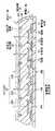
図5ないし図7はこの表示装置の製造方法を工程順に表すものである。まず、図5(A)に示したように、例えば、上述した材料よりなる封止用基板21の上に、上述した材料よりなる反射光吸収膜23を成膜し、図4のような形状にパターニングする。次いで、図5(B)に示したように、封止用基板21の上に、赤色フィルター22Rの材料をスピンコートなどにより塗布し、フォトリソグラフィ技術によりパターニングして焼成することにより赤色フィルター22Rを形成する。パターニングの際には、赤色フィルター22Rの周縁部が反射光吸収膜23にかかるようにすることが好ましい。反射光吸収膜23にかからないように高精度にパターニングすることは難しく、また反射光吸収膜23の上に重なった部分は画像表示に影響を与えないからである。続いて、図5(C)に示したように、赤色フィルター22Rと同様にして、青色フィルター22Bおよび緑色フィルター22Gを順次形成する。これにより封止パネル20が作製される。
【0033】
また、図6(A)に示したように、例えば、上述した材料よりなる駆動用基板11の上に、例えば直流スパッタリングにより、上述した材料よりなる複数の陽極12を並列に形成する。次いで、陽極12の上に、例えばCVD(Chemical Vapor Deposition ;化学的気相成長)法により絶縁層13を上述した厚みで成膜し、例えばリソグラフィー技術を用いて発光領域に対応する部分を選択的に除去して開口部13Aを形成する。
【0034】
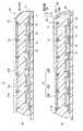
続いて、図6(B)に示したように、例えば蒸着法により図示しないエリアマスクを用い、絶縁層13の開口部13Aに対応して、上述した厚みおよび材料よりなる正孔注入層14A,正孔輸送層14B,発光層14Cおよび電子輸送層14Dを順次成膜する。その際、有機電界発光素子10R,10G,10Bにより用いるエリアマスクを代え、有機電界発光素子10R,10G,10Bごとに成膜をする。また、開口部13Aにのみ高精度に蒸着することは難しいので、開口部13A全体を覆い、絶縁層13の縁に少しかかるように成膜することが好ましい。有機層14を形成したのち、例えば蒸着法により図示しないエリアマスクを用い、上述した厚みおよび材料よりなる複数の半透過性電極15Aを、陽極12に対して垂直な方向に並列に形成する。そののち、半透過性電極15Aの上に、例えば直流スパッタリングにより、半透過性電極15Aと同じエリアマスクを用いて透明電極15Bを成膜する。これにより、駆動パネル10が形成される。
【0035】
封止パネル20および駆動パネル10を形成したのち、図6(C)に示したように、駆動用基板11の有機電界発光素子10R,10G,10Bを形成した側に、例えば熱硬化型樹脂を塗布することにより、接着層30のうち熱により硬化する部分30Bを形成する。塗布は、例えば、スリットノズル型ディスペンサーから樹脂を吐出させて行うようにしてもよく、ロールコートあるいはスクリーン印刷などにより行うようにしてもよい。接着層30の熱により硬化する部分30Bは、1液のみにより、または、2液の組合せにより、硬化を開始するものを用いることができる。なお、2液以上の組合せによる場合、塗布は同時に行っても良いし、別々に行っても良く、塗布の順序も任意である。塗布を同時に行う場合には、混合されたものを塗布するようにしてもよいし、同時に塗布されることにより混合されるようにしてもよい。別々に行う場合には、1液ずつ順次塗布した後に、例えば封止パネル20と駆動パネル10との貼合せによる圧力を加えることにより混合されるようにしてもよい。
【0036】
次いで、図7(A)に示したように、駆動パネル10と封止パネル20とを接着層30を介して貼り合わせる。その際、封止パネル20のうちカラーフィルタ22および反射光吸収膜23を形成した側の面を、駆動パネル10と対向させて配置することが好ましい。また、接着層30に気泡などが混入しないようにすることが好ましい。
【0037】
続いて、図7(B)に示したように、例えば封止パネル20を矢印で示したように移動させることにより、封止パネル20と駆動パネル10との相対位置を整合させる。すなわち、有機電界発光素子10R,10G,10Bとカラーフィルター22との位置を整合させる。このとき、接着層30はまだ未硬化であり、封止パネル20と駆動パネル10との相対位置を数百μm程度動かすことができる状態である。封止パネル20と駆動パネル10との相対位置を整合させて封止パネル20を仮固定する。この仮固定は、例えば、接着層30の周縁部の少なくとも一部に、封止パネル20および駆動パネル10の両方にまたがるように紫外線硬化型樹脂を塗布し、封止パネル20の側から紫外線UVを照射して紫外線硬化型樹脂を硬化させて仮固定部30Aを形成することにより行うことができる。
【0038】
最後に、図8に示したように、適切な温度に加熱することにより、接着層30を硬化させ、駆動パネル10と封止パネル20とを接着させる。硬化温度は、例えば80℃なら2時間、60℃なら4時間というように、加熱時間に応じて適切に定めることができる。以上により、図1ないし図4に示した表示装置が完成する。
【0039】
このようにして作製された表示装置では、陽極12と陰極15との間に所定の電圧が印加されると、発光層14Cに電流が注入され、正孔と電子とが再結合することにより、主として発光層14C側の界面において発光が起こる。この光は、陽極12と半透過性電極15Aとの間で多重反射し、陰極15,接着層30,カラーフィルター22および封止用基板21を透過して、封止パネル20の側から取り出される。本実施の形態では、封止パネル20にカラーフィルター22および反射光吸収膜23が設けられているので、封止パネル20から入射した外光が有機電界発光素子10R,10G,10Bなどで反射して封止パネル20から射出することが防止され、コントラストが向上する。
【0040】
また、本実施の形態では、有機電界発光素子10R,10G,10Bに、半透過性電極15Aと陽極12とを共振部とする共振器が構成されているので、多重干渉することにより、取り出される光のスペクトルの半値幅が小さくなり、色純度が向上すると共に、外光は減衰し、カラーフィルター22との組合せにより外光の反射率はより小さくなる。すなわち、よりコントラストが向上する。
【0041】
このように本実施の形態によれば、封止用基板21にカラーフィルター22を設け、有機電界発光素子10R,10G,10Bを覆うように設けた接着層30により、封止パネル20と駆動パネル10とを接着させるようにしたので、封止パネル20から入射した外光が有機電界発光素子10R,10G,10Bなどで反射し、封止パネル20から射出することを防止することができる。よって、コントラストを向上させることができる。また、接着層30により有機電界発光素子10R,10G,10Bを確実に封止することができ、有機電界発光素子10R,10G,10Bの腐食および破損を有効に防止することができる。更に、接着層30は熱により硬化するものであるので、接着力が強く安定な接着層30によって、駆動パネル10と封止パネル20とをカラーフィルター22の有無にかかわらず簡単に貼り合わせることができる。
【0042】
さらに、接着層30の周縁部の一部に仮固定部30Aを形成し、封止パネル20の相対位置を駆動パネル10に対して整合させるようにしたので、精度よいアラインメントが可能となる。また、仮固定部30Aは紫外線硬化型樹脂により構成されているため、低温で短時間硬化が可能であり、簡単かつ精確に仮固定を行うことができる。
【0043】
また、有機電界発光素子10R,10G,10Bが半透過性電極15Aと陽極12とを共振部とする共振器を有するようにすれば、発光層14Cで発生した光を多重干渉させ、一種の狭帯域フィルタとして作用させることにより、取り出す光のスペクトルの半値幅を減少させることができ、色純度を向上させることができる。更に、封止パネル20から入射した外光についても多重干渉により減衰させることができ、カラーフィルター22との組合せにより有機電界発光素子10R,10G,10Bにおける外光の反射率を極めて小さくすることができる。よって、コントラストをより向上させることができる。
【0044】
[第2の実施の形態]
図9は本発明の第2の実施の形態に係る表示装置を表すものである。この表示装置は、反射防止膜24を封止用基板21の駆動パネル10と反対側の表面に設けたことを除き、第1の実施の形態で説明した表示装置と同一である。したがって、同一の構成要素には同一の符号を付して、その詳細な説明を省略する。
【0045】
反射防止膜24は、封止用基板21における外光の表面反射を防止するためのものである。封止用基板21を例えばガラスにより構成した場合その表面反射は4%程度であるが、カラーフィルタ22および反射光吸収膜23などにより表示装置内部での外光反射を抑制すると、封止用基板21における表面反射も無視できなくなるからである。
【0046】
反射防止膜24は、例えば、酸化ケイ素(SiO2)と酸化チタン(TiO2)あるいは酸化ニオブ(Nb2O5)とを積層した薄膜フィルターにより構成することが好ましい。
【0047】
このように本実施の形態によれば、第1の実施の形態において説明した効果に加えて、封止用基板21に反射防止膜24を設けるようにしたので、封止用基板21における外光の表面反射を小さくすることができ、コントラストを更に向上させることができる。なお、接着層30は熱により硬化すること、およびその効果については上記実施の形態と同様である。
【0048】
以上、実施の形態を挙げて本発明を説明したが、本発明は上記実施の形態に限定されるものではなく、種々変形が可能である。例えば、上記実施の形態では、封止用基板21にカラーフィルター22および反射光吸収膜23を設ける場合について説明したが、反射光吸収膜23は必要に応じて設ければよく、設けなくてもよい。
【0049】
また、上記実施の形態では、接着層30を駆動パネル10の全面に設けるようにしたが、接着層30は、少なくとも有機電界発光素子10R,10G,10Bを覆うように設けられていればよい。さらに、上記実施の形態では、仮固定部30Aを、接着層30の周縁部の一部に設けるようにしたが、仮固定部30Aを、例えば接着層30の周縁部全体に、接着層30を取り囲むように形成してもよい。
【0050】
加えて、上記実施の形態では、有機電界発光素子10R,10G,10Bの構成を具体的に挙げて説明したが、絶縁層13あるいは透明電極15Bなどの全ての層を備える必要はなく、また、他の層を更に備えていてもよい。なお、半透過性電極15Aを備えない場合についても本発明を適用することができるが、上記実施の形態においても説明したように、半透過性電極15Aと陽極12とを共振部とする共振器を有するようにした方が、有機電界発光素子10R,10G,10Bにおける外光の反射率を小さくすることができ、コントラストをより向上させることができるので好ましい。
【0051】
更にまた、上記実施の形態では、第1電極を陽極とし第2電極を陰極としたが、第1電極を陰極とし第2電極を陽極とするようにしてもよい。この場合、陽極の側から光を取り出すようになり、陽極が半透過性電極あるいは透明電極などにより構成される。
【0052】
加えてまた、上記実施の形態では、有機層14の材料を変えることにより赤色,緑色および青色の光を発生させるようにしたが、本発明は、色変換層(color changing mediams;CCM)を組み合わせることにより、またはカラーフィルターを組み合わせることによりこれらの光を発生させるようにした表示装置についても、適用することができる。
【0053】
【発明の効果】
以上説明したように請求項1記載の表示装置の製造方法によれば、有機電界発光素子を有する駆動基板と、カラーフィルターを有する封止用基板とを少なくとも熱により硬化する接着層により接着させるようにしたので、接着力が強く安定な接着層によって、駆動パネルと封止パネルとを簡単に貼り合わせることができ、第2電極側から光を取り出すタイプの表示装置を容易に実現することができる。
【0054】
特に、接着層の周縁部の少なくとも一部に仮固定部を形成し、この仮固定部が封止パネルおよび駆動パネルの両方にまたがるように形成され、封止パネルの相対位置を駆動パネルに対して整合させるようにしたので、精度よいアラインメントが可能となる。
【0055】
また、仮固定部は紫外線硬化型樹脂により構成されているので、低温で短時間硬化が可能であり、簡単かつ精確に仮固定を行うことができる。
【0056】
加えて、封止用基板に反射防止膜を設けるようにすれば、封止用基板における外光の表面反射を小さくすることができ、コントラストを更に向上させることができる。
【0057】
更に、半透過性電極と第1電極とが共振器の共振部を構成するようにすれば、発光層で発生した光を多重干渉させ、一種の狭帯域フィルタとして作用させることにより、取り出す光のスペクトルの半値幅を減少させることができ、色純度を向上させることができる。加えて、封止パネルから入射した外光についても多重干渉により減衰させることができ、カラーフィルターとの組合せにより有機電界発光素子における外光の反射率を極めて小さくすることができる。よって、コントラストをより向上させることができる。
【図面の簡単な説明】
【図1】本発明の第1の実施の形態に係る表示装置の構成を表す断面図である。
【図2】図1に示した表示装置における有機電界発光素子の構成を拡大して表す断面図である。
【図3】図1に示した表示装置における有機電界発光素子の構成を拡大して表す断面図である。
【図4】図1に示した表示装置におけるカラーフィルターの構成を表す駆動パネルの側から見た平面図である。
【図5】図1に示した表示装置の製造方法を工程順に表す断面図である。
【図6】図5に続く工程を表す断面図である。
【図7】図6に続く工程を表す断面図である。
【図8】図7に続く工程を表す断面図である。
【図9】本発明の第2の実施の形態に係る表示装置の構成を表す断面図である。
【符号の説明】
10…駆動パネル、10R,10G,10B…有機電界発光素子、11…駆動用基板、12…陽極(第1電極)、13…絶縁層、13A…開口部、14…有機層、14A…正孔注入層、14B…正孔輸送層、14C…発光層、14D…電子輸送層、15…陰極(第2電極)、15A…半透過性電極、15B…透明電極、20…封止パネル、21…封止用基板、22…カラーフィルター、22R…赤色フィルター、22G…緑色フィルター、22B…青色フィルター、23…反射光吸収膜、24…反射防止膜、30…接着層、30A…仮固定部(紫外線硬化型樹脂)、30B…熱により硬化した部分[0001]
BACKGROUND OF THE INVENTION
The present invention relates to a display device in which a driving panel in which an organic electroluminescence element (organic EL; electroluminescence element) is provided on a driving substrate and a sealing panel are bonded together via an adhesive layer.of It relates to a manufacturing method.
[0002]
[Prior art]
In recent years, organic EL displays using organic electroluminescent elements have attracted attention as display devices that replace liquid crystal displays. Organic EL displays are self-luminous and have a wide viewing angle and low power consumption. Also, they are considered to have sufficient response to high-definition high-speed video signals. Development is underway for practical application.
[0003]
As an organic electroluminescent element, for example, a device in which a first electrode, an organic layer including a light emitting layer, and a second electrode are sequentially laminated on a driving substrate is known. The organic electroluminescent element is sealed by a sealing substrate disposed opposite to the driving substrate via an adhesive layer made of, for example, an ultraviolet curable resin (for example, Japanese Patent Laid-Open No. 5-182759, JP-A-11-40345, JP-A-11-297476, JP-A-2000-68049, etc.). Further, the organic electroluminescent element is usually covered with, for example, an inorganic protective film in order to prevent the occurrence of a non-light emitting region (dark spot) (for example, Japanese Patent Laid-Open Nos. 11-40345 and 11). No. -297476, JP 2000-68049 A, Japanese Patent No. 3170542, etc.). In such an organic electroluminescent element, the light generated in the light emitting layer may be extracted from the driving substrate side depending on the type of display, but may be extracted from the second electrode side.
[0004]
By the way, in the organic EL display using such an organic electroluminescent element, there is a problem that external light reflection is large in the organic electroluminescent element and the wiring electrode between the elements, and the contrast as a display is lowered. Therefore, a method of preventing external light reflection by arranging a color filter or a reflected light absorbing film has been considered. Here, in a display of a type in which light is extracted from the side of the driving substrate, a color filter or the like is disposed on the driving substrate, an ultraviolet curable resin layer is formed on the driving substrate, cured, and then organic electroluminescence An element forming element has been reported (Japanese Patent Laid-Open No. 11-260562). In addition, after the organic electroluminescent element is formed on the driving substrate, the organic electroluminescent element is sealed with an ultraviolet curable resin layer and a sealing substrate, and a color filter is provided on the driving substrate side. It has been reported that a substrate is disposed and a driving substrate and an auxiliary substrate are bonded by a layer of an ultraviolet curable resin disposed only at the peripheral portion (Japanese Patent Laid-Open No. 11-345688).
[0005]
[Problems to be solved by the invention]
On the other hand, in the type of display in which light is extracted from the second electrode side, a color filter is provided on the sealing substrate side for sealing the organic electroluminescent element. However, in this type of display, the color filter and the reflected light absorbing film have a low transmittance of ultraviolet light having a wavelength of 430 nm or less, so that an ultraviolet curable resin is used as in the conventional type in which light is extracted from the driving substrate side. Therefore, it was difficult to cover the organic electroluminescent element and attach the sealing substrate together.
[0006]
The present invention has been made in view of such problems, and its purpose is to extract light from the second electrode side, a drive panel having an organic electroluminescent element, a sealing panel having a color filter, and the like. Display device for easy bondingof It is to provide a manufacturing method.
[0007]
[Means for Solving the Problems]
In the method for manufacturing a display device according to the present invention, a plurality of organic electroluminescent elements are provided by sequentially laminating a first electrode, one or more organic layers including a light emitting layer, and a second electrode on a driving substrate. A step of forming a driving panel for extracting generated light from the second electrode side, a step of forming a sealing panel by disposing a color filter on a sealing substrate, and a driving panelMultiple of le A step of providing a thermosetting resin as an adhesive layer so as to cover the organic electroluminescence device, a step of bonding the driving panel and the sealing panel with the thermosetting resin in between, and a driving by moving the sealing panel After aligning the relative position with the panel, at least part of the peripheral edge of the thermosetting resin is provided with UV curable resin across both the sealing panel and the drive panel, and the UV curable resin is sealed with the sealing panel. Irradiating ultraviolet rays from the side to form a temporary fixing part,After forming the temporary fixing part, And a step of curing the thermosetting resin.
[0008]
In the method for manufacturing a display device according to the present invention, a plurality of organic electroluminescent elements are provided by sequentially laminating a first electrode, one or more organic layers including a light emitting layer, and a second electrode on a driving substrate, and the light emitting layer is provided. A drive panel for taking out the light generated in
[0009]
DETAILED DESCRIPTION OF THE INVENTION
Hereinafter, embodiments of the present invention will be described in detail with reference to the drawings.
[0010]
[First Embodiment]
FIG. 1 shows a cross-sectional structure of a display device according to a first embodiment of the present invention. This display device is used as an ultra-thin organic EL color display device or the like. For example, the
[0011]
In the organic
[0012]
The
[0013]
The
[0014]
The
[0015]
In the
[0016]
In the
[0017]
FIG. 3 shows an enlarged configuration of the
[0018]
In the
[0019]
As shown in FIGS. 2 and 3, the
[0020]
The
[0021]
For this purpose, it is preferable to match the peak wavelength of the narrow band filter with the peak wavelength of the spectrum of light to be extracted. That is, the phase shift of the reflected light generated at the
[0022]
[Expression 2]
2L / λ + Φ / 2π = q (q is an integer)
[0023]
The transparent electrode 15B is for lowering the electric resistance of the
[0024]
As shown in FIG. 1, the sealing
[0025]
The
[0026]
FIG. 4 shows a planar configuration of the
[0027]
The
[0028]
As shown in FIGS. 1 and 4, the reflected
[0029]
As shown in FIG. 1, the
[0030]
A
[0031]
This display device can be manufactured, for example, as follows.
[0032]
5 to 7 show the manufacturing method of this display device in the order of steps. First, as shown in FIG. 5A, for example, a reflected
[0033]
Also, as shown in FIG. 6A, for example, a plurality of
[0034]
Subsequently, as shown in FIG. 6B, the
[0035]
After forming the sealing
[0036]
Next, as shown in FIG. 7A, the
[0037]
Subsequently, as illustrated in FIG. 7B, for example, the sealing
[0038]
Finally, as shown in FIG. 8, the
[0039]
In the display device thus manufactured, when a predetermined voltage is applied between the
[0040]
In the present embodiment, the
[0041]
Thus, according to the present embodiment, the
[0042]
Furthermore, since the
[0043]
In addition, if the
[0044]
[Second Embodiment]
FIG. 9 shows a display device according to the second embodiment of the present invention. This display device is the same as the display device described in the first embodiment, except that the
[0045]
The
[0046]
The
[0047]
As described above, according to the present embodiment, in addition to the effects described in the first embodiment, the
[0048]
While the present invention has been described with reference to the embodiment, the present invention is not limited to the above embodiment, and various modifications can be made. For example, in the above embodiment, the case where the
[0049]
In the above embodiment, the
[0050]
In addition, in the above-described embodiment, the configuration of the
[0051]
Furthermore, in the above embodiment, the first electrode is an anode and the second electrode is a cathode. However, the first electrode may be a cathode and the second electrode may be an anode. In this case, light is extracted from the anode side, and the anode is constituted by a semi-transmissive electrode or a transparent electrode.
[0052]
In addition, in the above-described embodiment, red, green and blue light is generated by changing the material of the
[0053]
【The invention's effect】
As described above, the display device according to claim 1of According to the manufacturing method, the driving substrate having the organic electroluminescent element and the sealing substrate having the color filter are adhered to each other by the adhesive layer that is cured at least by heat. The drive panel and the sealing panel can be easily pasted together, and a display device of the type that extracts light from the second electrode side can be easily realized.
[0054]
SpecialTo A temporary fixing part is formed on at least a part of the peripheral edge of the deposition layer, and the temporary fixing part is formed so as to extend over both the sealing panel and the driving panel, and the relative position of the sealing panel is aligned with the driving panel. As a result, it is possible to perform accurate alignment.
[0055]
MaTentative Since the fixing portion is made of an ultraviolet curable resin, it can be cured at a low temperature for a short time, and temporary fixing can be performed easily and accurately.
[0056]
In additionSeal An anti-reflection film is provided on the stop substrateif The surface reflection of external light on the sealing substrate can be reduced, and the contrast can be further improved.
[0057]
FurtherHalf The transmissive electrode and the first electrode constitute a resonance part of the resonator.if By causing multiple interference of the light generated in the light emitting layer and acting as a kind of narrow band filter, the half width of the spectrum of the extracted light can be reduced, and the color purity can be improved. In addition, the external light incident from the sealing panel can also be attenuated by multiple interference, and the reflectance of the external light in the organic electroluminescent element can be extremely reduced by combining with the color filter. Therefore, the contrast can be further improved.
[Brief description of the drawings]
FIG. 1 is a cross-sectional view illustrating a configuration of a display device according to a first embodiment of the invention.
2 is an enlarged cross-sectional view showing a configuration of an organic electroluminescent element in the display device shown in FIG.
3 is an enlarged cross-sectional view showing a configuration of an organic electroluminescent element in the display device shown in FIG.
4 is a plan view showing a configuration of a color filter in the display device shown in FIG. 1 as viewed from the drive panel side.
5 is a cross-sectional view illustrating a method of manufacturing the display device illustrated in FIG. 1 in the order of steps.
6 is a cross-sectional diagram illustrating a process following the process in FIG. 5. FIG.
7 is a cross-sectional view illustrating a process following the process in FIG. 6. FIG.
8 is a cross-sectional view illustrating a process following FIG.
FIG. 9 is a cross-sectional view illustrating a configuration of a display device according to a second embodiment of the invention.
[Explanation of symbols]
DESCRIPTION OF
Claims (1)
Translated fromJapanese封止用基板にカラーフィルターを配設して封止パネルを形成する工程と、
前記駆動パネルの前記複数の有機電界発光素子を覆うように接着層としての熱硬化型樹脂を設ける工程と、
前記熱硬化型樹脂を間にして前記駆動パネルと前記封止パネルとを貼り合わせる工程と、
前記封止パネルを移動させて前記駆動パネルとの相対位置を整合させたのち、前記熱硬化型樹脂の周縁部の少なくとも一部に、前記封止パネルおよび前記駆動パネルの両方にまたがって紫外線硬化型樹脂を設け、前記紫外線硬化型樹脂に前記封止パネルの側から紫外線を照射して仮固定部を形成する工程と、
前記仮固定部を形成したのち、前記熱硬化型樹脂を硬化させる工程と
を含むことを特徴とする表示装置の製造方法。A plurality of organic electroluminescent elements are provided by sequentially laminating a first electrode, one or more organic layers including a light emitting layer, and a second electrode on a driving substrate, and light generated in the light emitting layer is emitted from the second electrode. Forming a drive panel to be taken out from the side;
A step of arranging a color filter on the sealing substrate to form a sealing panel;
A step of providing a thermosetting resin as an adhesive layer to coverthe plurality of organic electroluminescent elementsof the drivepanel,
Bonding the drive panel and the sealing panel with the thermosetting resin in between,
After moving the sealing panel and aligning the relative position with the drive panel, at least part of the periphery of the thermosetting resin is UV cured across both the sealing panel and the drive panel. Providing a mold resin, and irradiating the ultraviolet curable resin with ultraviolet rays from the sealing panel side to form a temporary fixing part;
And a step of curing the thermosetting resinafter forming the temporary fixing portion .
Priority Applications (24)
| Application Number | Priority Date | Filing Date | Title |
|---|---|---|---|
| JP2002059040AJP3724725B2 (en) | 2001-11-01 | 2002-03-05 | Manufacturing method of display device |
| KR1020027012906AKR20040044065A (en) | 2001-11-01 | 2002-05-13 | Display apparatus |
| US10/240,358US7071619B2 (en) | 2001-11-01 | 2002-05-13 | Display apparatus comprising temporary fixing portion adjacent an adhesive layer |
| DE60226993TDE60226993D1 (en) | 2001-11-01 | 2002-05-13 | Display |
| CN200710111866XACN101080117B (en) | 2001-11-01 | 2002-05-13 | Display apparatus |
| TW091109891ATWI279162B (en) | 2001-11-01 | 2002-05-13 | Display apparatus |
| CNB028002032ACN100350624C (en) | 2001-11-01 | 2002-05-13 | Display device |
| KR1020097000490AKR100921285B1 (en) | 2001-11-01 | 2002-05-13 | Display apparatus |
| PCT/JP2002/004611WO2003039203A1 (en) | 2001-11-01 | 2002-05-13 | Display |
| KR1020097000496AKR100921284B1 (en) | 2001-11-01 | 2002-05-13 | Manufacturing method of display apparatus |
| EP02724771AEP1441571B1 (en) | 2001-11-01 | 2002-05-13 | Display |
| US11/441,874US7282856B2 (en) | 2001-11-01 | 2006-05-26 | Electroluminescent display having an adhesive layer comprised of two or more liquids |
| US11/899,489US7828617B2 (en) | 2001-11-01 | 2007-09-06 | Display apparatus |
| US12/873,983US8179038B2 (en) | 2001-11-01 | 2010-09-01 | Display apparatus |
| US13/456,320US8519622B2 (en) | 2001-11-01 | 2012-04-26 | Display apparatus |
| US13/707,194US20130099217A1 (en) | 2001-11-01 | 2012-12-06 | Display apparatus |
| US14/185,574US8896203B2 (en) | 2001-11-01 | 2014-02-20 | Display apparatus including a plurality of organic electroluminescent devices |
| US14/498,349US9425427B2 (en) | 2001-11-01 | 2014-09-26 | Display apparatus including organic electroluminescent devices |
| US15/221,204US9653699B2 (en) | 2001-11-01 | 2016-07-27 | Method of manufacturing a display apparatus |
| US15/221,197US9716246B2 (en) | 2001-11-01 | 2016-07-27 | Display apparatus |
| US15/637,514US10008688B2 (en) | 2001-11-01 | 2017-06-29 | Display apparatus including organic electroluminescence devices |
| US15/993,026US10249841B2 (en) | 2001-11-01 | 2018-05-30 | Display apparatus |
| US16/276,155US10930877B2 (en) | 2001-11-01 | 2019-02-14 | Display apparatus including organic electroluminescence devices |
| US17/151,215US11258036B2 (en) | 2001-11-01 | 2021-01-18 | Display apparatus including organic electroluminescence devices |
Applications Claiming Priority (3)
| Application Number | Priority Date | Filing Date | Title |
|---|---|---|---|
| JP2001336772 | 2001-11-01 | ||
| JP2001-336772 | 2001-11-01 | ||
| JP2002059040AJP3724725B2 (en) | 2001-11-01 | 2002-03-05 | Manufacturing method of display device |
Publications (2)
| Publication Number | Publication Date |
|---|---|
| JP2003203762A JP2003203762A (en) | 2003-07-18 |
| JP3724725B2true JP3724725B2 (en) | 2005-12-07 |
Family
ID=26624292
Family Applications (1)
| Application Number | Title | Priority Date | Filing Date |
|---|---|---|---|
| JP2002059040AExpired - LifetimeJP3724725B2 (en) | 2001-11-01 | 2002-03-05 | Manufacturing method of display device |
Country Status (8)
| Country | Link |
|---|---|
| US (14) | US7071619B2 (en) |
| EP (1) | EP1441571B1 (en) |
| JP (1) | JP3724725B2 (en) |
| KR (3) | KR100921285B1 (en) |
| CN (2) | CN101080117B (en) |
| DE (1) | DE60226993D1 (en) |
| TW (1) | TWI279162B (en) |
| WO (1) | WO2003039203A1 (en) |
Families Citing this family (70)
| Publication number | Priority date | Publication date | Assignee | Title |
|---|---|---|---|---|
| TW468283B (en) | 1999-10-12 | 2001-12-11 | Semiconductor Energy Lab | EL display device and a method of manufacturing the same |
| TW471011B (en) | 1999-10-13 | 2002-01-01 | Semiconductor Energy Lab | Thin film forming apparatus |
| JP3804858B2 (en)* | 2001-08-31 | 2006-08-02 | ソニー株式会社 | Organic electroluminescent device and manufacturing method thereof |
| JP3724725B2 (en)* | 2001-11-01 | 2005-12-07 | ソニー株式会社 | Manufacturing method of display device |
| JP3705264B2 (en)* | 2001-12-18 | 2005-10-12 | セイコーエプソン株式会社 | Display device and electronic device |
| US7242140B2 (en)* | 2002-05-10 | 2007-07-10 | Seiko Epson Corporation | Light emitting apparatus including resin banks and electronic device having same |
| US6911772B2 (en)* | 2002-06-12 | 2005-06-28 | Eastman Kodak Company | Oled display having color filters for improving contrast |
| JP3703028B2 (en)* | 2002-10-04 | 2005-10-05 | ソニー株式会社 | Display element and display device using the same |
| US7336029B2 (en)* | 2003-07-31 | 2008-02-26 | Optrex Corporation | Organic EL display having convex portion with color layers |
| US6905788B2 (en)* | 2003-09-12 | 2005-06-14 | Eastman Kodak Company | Stabilized OLED device |
| JP4895490B2 (en)* | 2003-09-30 | 2012-03-14 | 三洋電機株式会社 | Organic EL panel |
| JP4595955B2 (en)* | 2003-10-23 | 2010-12-08 | セイコーエプソン株式会社 | Organic EL device manufacturing method, organic EL device, and electronic apparatus |
| CN100489569C (en) | 2003-10-28 | 2009-05-20 | 株式会社半导体能源研究所 | Method of manufacturing optical film |
| WO2005052893A1 (en) | 2003-11-28 | 2005-06-09 | Semiconductor Energy Laboratory Co., Ltd. | Method of manufacturing display device |
| US7019331B2 (en)* | 2004-01-22 | 2006-03-28 | Eastman Kodak Company | Green light-emitting microcavity OLED device using a yellow color filter element |
| KR101087567B1 (en)* | 2004-03-23 | 2011-11-28 | 엘지디스플레이 주식회사 | Organic electroluminescent device and manufacturing method thereof |
| KR101127061B1 (en)* | 2004-04-08 | 2012-03-26 | 글로벌 오엘이디 테크놀러지 엘엘씨 | Oled with color change media |
| US7057339B2 (en)* | 2004-04-08 | 2006-06-06 | Eastman Kodak Company | OLED with color change media |
| US7915822B2 (en)* | 2004-08-04 | 2011-03-29 | Samsung Electronics Co., Ltd. | Display device and method and apparatus for manufacturing the same |
| US20060049751A1 (en)* | 2004-09-07 | 2006-03-09 | Jiun-Haw Lee | Display device with dual display areas |
| US20080068849A1 (en)* | 2004-10-28 | 2008-03-20 | Polaris Industries Inc. | ATV worklight |
| JP4238822B2 (en)* | 2004-12-03 | 2009-03-18 | セイコーエプソン株式会社 | Pattern-formed substrate, electro-optical device, pattern-formed substrate manufacturing method, and electro-optical device manufacturing method |
| KR100638040B1 (en)* | 2004-12-06 | 2006-10-23 | 엘지전자 주식회사 | Cap for Organic Electroluminescent Device |
| JP2006245010A (en)* | 2005-01-31 | 2006-09-14 | Tdk Corp | Panel |
| JP2006236996A (en)* | 2005-01-31 | 2006-09-07 | Tdk Corp | panel |
| JP4017007B2 (en)* | 2005-03-29 | 2007-12-05 | エプソンイメージングデバイス株式会社 | Electro-optical device and electronic apparatus including the electro-optical device |
| GB0510282D0 (en)* | 2005-05-20 | 2005-06-29 | Cambridge Display Tech Ltd | Top-electroluminescent devices comprising cathode bus bars |
| US20060290276A1 (en)* | 2005-06-22 | 2006-12-28 | Eastman Kodak Company | OLED device having spacers |
| JP5046521B2 (en)* | 2006-01-18 | 2012-10-10 | 株式会社半導体エネルギー研究所 | Light emitting device |
| KR100645705B1 (en)* | 2006-01-27 | 2006-11-15 | 삼성에스디아이 주식회사 | Organic light emitting display device and manufacturing method |
| JP2007287669A (en)* | 2006-03-23 | 2007-11-01 | Canon Inc | Organic light emitting device and method for manufacturing organic light emitting device |
| CN101083275B (en)* | 2006-05-30 | 2010-12-01 | 奇美电子股份有限公司 | Display image system |
| US7659664B2 (en) | 2006-05-30 | 2010-02-09 | Tpo Displays Corp. | System for displaying image |
| JP4337852B2 (en) | 2006-08-30 | 2009-09-30 | セイコーエプソン株式会社 | ORGANIC ELECTROLUMINESCENT DEVICE, ITS MANUFACTURING METHOD, AND ELECTRONIC DEVICE |
| JP2008066216A (en)* | 2006-09-11 | 2008-03-21 | Seiko Epson Corp | ORGANIC ELECTROLUMINESCENT DEVICE, ITS MANUFACTURING METHOD, AND ELECTRONIC DEVICE |
| JP4752714B2 (en)* | 2006-10-13 | 2011-08-17 | セイコーエプソン株式会社 | LIGHT EMITTING DEVICE AND ELECTRONIC DEVICE |
| KR100829750B1 (en) | 2006-12-06 | 2008-05-15 | 삼성에스디아이 주식회사 | Organic light emitting display |
| KR100829753B1 (en) | 2007-03-02 | 2008-05-15 | 삼성에스디아이 주식회사 | Organic light emitting display |
| JP5470689B2 (en)* | 2007-08-30 | 2014-04-16 | ソニー株式会社 | Display device |
| DE102008019902A1 (en)* | 2007-12-21 | 2009-06-25 | Osram Opto Semiconductors Gmbh | Optoelectronic component and production method for an optoelectronic component |
| JP2010080224A (en) | 2008-09-25 | 2010-04-08 | Sony Corp | Method of manufacturing optical component, and optical component, as well as method of manufacturing display device, and display device |
| US9070900B2 (en)* | 2008-11-13 | 2015-06-30 | Joled Inc | Method of manufacturing display, and display |
| TWI477592B (en)* | 2008-11-28 | 2015-03-21 | Mitsui Chemicals Inc | Organic EL surface sealant, display device manufacturing method, and display device |
| WO2010131171A2 (en)* | 2009-05-14 | 2010-11-18 | Koninklijke Philips Electronics N.V. | Short circuit prevention in electroluminescent devices |
| US8246867B2 (en)* | 2009-10-16 | 2012-08-21 | Corning Incorporated | Method for assembling an optoelectronic device |
| KR101084179B1 (en) | 2009-12-28 | 2011-11-17 | 삼성모바일디스플레이주식회사 | Sealing method of organic light emitting display device |
| TWI514916B (en)* | 2010-03-17 | 2015-12-21 | Innolux Corp | Image display system |
| CN102194851B (en)* | 2010-03-17 | 2016-01-20 | 群创光电股份有限公司 | Image display system |
| JP5654590B2 (en)* | 2010-06-16 | 2015-01-14 | パナソニック株式会社 | EL display panel, EL display device provided with EL display panel, organic EL display device, and method of manufacturing EL display panel |
| KR101356871B1 (en)* | 2010-06-16 | 2014-01-28 | 파나소닉 주식회사 | El display panel, el display device provided with el display panel, organic el display device, and method for manufacturing el display panel |
| JP5459142B2 (en)* | 2010-08-11 | 2014-04-02 | セイコーエプソン株式会社 | ORGANIC EL DEVICE, METHOD FOR MANUFACTURING ORGANIC EL DEVICE, AND ELECTRONIC DEVICE |
| CN104409021B (en)* | 2010-10-14 | 2017-01-18 | 上海聚然智能科技有限公司 | layered electroluminescent material screen |
| CN102446456B (en)* | 2010-10-14 | 2015-03-04 | 上海本星电子科技有限公司 | Layered electroluminescence display screen and stereoscopic display based on layered electroluminescence |
| CN102456297B (en)* | 2010-10-14 | 2016-07-06 | 上海科斗电子科技有限公司 | Laminated LED displays and stereoscopic displays based on LED technology |
| CN104282233B (en)* | 2010-10-14 | 2017-05-31 | 上海本星电子科技有限公司 | Hybrid display device and its application |
| JP5720887B2 (en)* | 2011-03-30 | 2015-05-20 | ソニー株式会社 | Display device and electronic device |
| KR101271413B1 (en)* | 2011-12-09 | 2013-06-05 | 한국과학기술원 | High contrast organic light emitting device and display apparatus comprising the same |
| CN103247236A (en)* | 2012-02-08 | 2013-08-14 | 上海科斗电子科技有限公司 | Dot-matrix LED (light-emitting diode) display screen and stereoscopic displayer based on LED technology |
| CN103296053A (en)* | 2012-03-05 | 2013-09-11 | 联胜(中国)科技有限公司 | Organic electroluminescence display device |
| US9155135B2 (en) | 2012-04-18 | 2015-10-06 | Joled Inc. | Display device and method for manufacturing display device |
| KR101945202B1 (en)* | 2012-08-14 | 2019-02-08 | 삼성디스플레이 주식회사 | Organic light emitting display device |
| JP2014153425A (en)* | 2013-02-05 | 2014-08-25 | Sony Corp | Display device, method for manufacturing display device, and electronic device |
| WO2014136213A1 (en)* | 2013-03-06 | 2014-09-12 | 株式会社 日立製作所 | Light source apparatus and method for manufacturing same |
| KR101466832B1 (en) | 2013-06-28 | 2014-11-28 | 코닝정밀소재 주식회사 | Oled |
| JP6191287B2 (en)* | 2013-07-05 | 2017-09-06 | ソニー株式会社 | Display device |
| JP6520065B2 (en)* | 2014-11-19 | 2019-05-29 | 大日本印刷株式会社 | Organic LED display device with color filter, method of manufacturing the same, and color filter with antireflective layer |
| JP2016133590A (en) | 2015-01-19 | 2016-07-25 | ソニー株式会社 | Display device and electronic apparatus |
| KR102354969B1 (en) | 2015-02-05 | 2022-01-25 | 삼성디스플레이 주식회사 | Organic light emitting display apparatus |
| KR101797018B1 (en)* | 2015-11-30 | 2017-11-13 | 엘지디스플레이 주식회사 | Organic light emitting display device and head mounted display including the same |
| CN109148706B (en)* | 2018-08-29 | 2021-10-26 | 京东方科技集团股份有限公司 | Light emitting device, method of manufacturing the same, and display apparatus |
Family Cites Families (52)
| Publication number | Priority date | Publication date | Assignee | Title |
|---|---|---|---|---|
| JPS63105493A (en)* | 1986-10-22 | 1988-05-10 | アルプス電気株式会社 | Thin film el panel |
| JPH04212287A (en)* | 1990-05-29 | 1992-08-03 | Toppan Printing Co Ltd | Organic thin film EL device |
| JPH05182759A (en) | 1991-12-26 | 1993-07-23 | Pioneer Video Corp | Organic EL element |
| JP2002000885A (en) | 1993-05-20 | 2002-01-08 | Le Tekku:Kk | Microcomputer chip for gaming machine control |
| JPH07142173A (en) | 1993-11-22 | 1995-06-02 | Toshiba Electron Eng Corp | Organic dispersion type EL panel |
| JP3170542B2 (en) | 1993-12-08 | 2001-05-28 | 出光興産株式会社 | Organic EL device |
| JP2589290Y2 (en) | 1993-12-24 | 1999-01-27 | オリンパス光学工業株式会社 | Parts mounting screw structure |
| JPH07320865A (en) | 1994-05-23 | 1995-12-08 | Matsushita Electric Ind Co Ltd | Organic thin film EL device and manufacturing method thereof |
| US5757127A (en)* | 1994-06-10 | 1998-05-26 | Nippondenso Co., Ltd. | Transparent thin-film EL display apparatus with ambient light adaptation means |
| JP3962436B2 (en)* | 1995-02-14 | 2007-08-22 | 出光興産株式会社 | Multicolor light emitting device |
| US5909081A (en)* | 1995-02-06 | 1999-06-01 | Idemitsu Kosan Co., Ltd. | Multi-color light emission apparatus with organic electroluminescent device |
| JP2838063B2 (en)* | 1995-09-20 | 1998-12-16 | 出光興産株式会社 | Organic electroluminescence device |
| US5780174A (en)* | 1995-10-27 | 1998-07-14 | Kabushiki Kaisha Toyota Chuo Kenkyusho | Micro-optical resonator type organic electroluminescent device |
| US5869929A (en)* | 1997-02-04 | 1999-02-09 | Idemitsu Kosan Co., Ltd. | Multicolor luminescent device |
| JP3743876B2 (en)* | 1997-07-16 | 2006-02-08 | カシオ計算機株式会社 | Electroluminescent device and manufacturing method thereof |
| JP3354444B2 (en) | 1997-07-16 | 2002-12-09 | 三洋電機株式会社 | Organic electroluminescence device |
| JP2845239B1 (en)* | 1997-12-17 | 1999-01-13 | 日本電気株式会社 | Organic thin film EL device and manufacturing method thereof |
| JPH11185955A (en)* | 1997-12-22 | 1999-07-09 | Tdk Corp | Organic EL color display |
| JPH11260562A (en) | 1998-03-09 | 1999-09-24 | Tdk Corp | Organic el color display |
| TW459032B (en)* | 1998-03-18 | 2001-10-11 | Sumitomo Bakelite Co | An anisotropic conductive adhesive and method for preparation thereof and an electronic apparatus using said adhesive |
| JP3775048B2 (en) | 1998-04-14 | 2006-05-17 | 松下電器産業株式会社 | Organic light emitting device |
| JPH11327448A (en)* | 1998-05-12 | 1999-11-26 | Idemitsu Kosan Co Ltd | Display device |
| JPH11345688A (en) | 1998-06-01 | 1999-12-14 | Tdk Corp | Organic el display |
| JP4037546B2 (en)* | 1998-10-26 | 2008-01-23 | シャープ株式会社 | Method for bonding translucent substrate |
| US6111357A (en)* | 1998-07-09 | 2000-08-29 | Eastman Kodak Company | Organic electroluminescent display panel having a cover with radiation-cured perimeter seal |
| JP2000068069A (en)* | 1998-08-13 | 2000-03-03 | Idemitsu Kosan Co Ltd | Organic electroluminescence device and method of manufacturing the same |
| JP2000068049A (en) | 1998-08-24 | 2000-03-03 | Casio Comput Co Ltd | Electroluminescent device and method of manufacturing the same |
| US6103541A (en)* | 1998-10-29 | 2000-08-15 | Industrial Technology Research Institute | Encapsulation method of an organic electroluminescent device |
| JP2000294369A (en)* | 1999-04-05 | 2000-10-20 | Chisso Corp | Organic EL device |
| JP2001035653A (en)* | 1999-07-21 | 2001-02-09 | Nec Corp | Organic EL panel and its filter |
| JP2001068271A (en)* | 1999-08-24 | 2001-03-16 | Fuji Photo Film Co Ltd | Light emitting element |
| TW522453B (en)* | 1999-09-17 | 2003-03-01 | Semiconductor Energy Lab | Display device |
| JP4942867B2 (en)* | 1999-09-17 | 2012-05-30 | 株式会社半導体エネルギー研究所 | EL display device and electronic device |
| US6624570B1 (en)* | 1999-09-29 | 2003-09-23 | Sanyo Electric Co., Ltd. | Electroluminescent display device and method for its fabrication |
| JP2001100668A (en)* | 1999-09-29 | 2001-04-13 | Sanyo Electric Co Ltd | Electroluminescence display device |
| TW466889B (en)* | 1999-11-22 | 2001-12-01 | Sony Corp | Display device |
| TW465122B (en)* | 1999-12-15 | 2001-11-21 | Semiconductor Energy Lab | Light-emitting device |
| TW493152B (en)* | 1999-12-24 | 2002-07-01 | Semiconductor Energy Lab | Electronic device |
| TW494447B (en) | 2000-02-01 | 2002-07-11 | Semiconductor Energy Lab | Semiconductor device and manufacturing method thereof |
| JP2001230072A (en)* | 2000-02-18 | 2001-08-24 | Denso Corp | Organic el display device |
| JP2001267070A (en)* | 2000-03-22 | 2001-09-28 | Sharp Corp | Method for manufacturing color EL display device |
| US7579203B2 (en)* | 2000-04-25 | 2009-08-25 | Semiconductor Energy Laboratory Co., Ltd. | Light emitting device |
| JP4327334B2 (en) | 2000-05-29 | 2009-09-09 | 三菱電機株式会社 | Heating control device, heat storage system, heating control method, and computer-readable recording medium recording a program for causing a computer to execute the method |
| JP2002008853A (en) | 2000-06-16 | 2002-01-11 | Nippon Seiki Co Ltd | Organic EL panel |
| JP4433577B2 (en) | 2000-06-20 | 2010-03-17 | 日本精機株式会社 | Organic EL panel |
| US6517958B1 (en)* | 2000-07-14 | 2003-02-11 | Canon Kabushiki Kaisha | Organic-inorganic hybrid light emitting devices (HLED) |
| JP2002059040A (en) | 2000-08-22 | 2002-02-26 | Yamaho Giken Kk | Pressure accumulation type spraying apparatus |
| JP4798322B2 (en)* | 2001-01-26 | 2011-10-19 | ソニー株式会社 | Display device and manufacturing method of display device |
| TW517356B (en)* | 2001-10-09 | 2003-01-11 | Delta Optoelectronics Inc | Package structure of display device and its packaging method |
| JP3724725B2 (en)* | 2001-11-01 | 2005-12-07 | ソニー株式会社 | Manufacturing method of display device |
| JP2003234186A (en)* | 2001-12-06 | 2003-08-22 | Sony Corp | Display device and method of manufacturing the same |
| TW515062B (en)* | 2001-12-28 | 2002-12-21 | Delta Optoelectronics Inc | Package structure with multiple glue layers |
- 2002
- 2002-03-05JPJP2002059040Apatent/JP3724725B2/ennot_activeExpired - Lifetime
- 2002-05-13KRKR1020097000490Apatent/KR100921285B1/ennot_activeExpired - Lifetime
- 2002-05-13CNCN200710111866XApatent/CN101080117B/ennot_activeExpired - Lifetime
- 2002-05-13KRKR1020027012906Apatent/KR20040044065A/ennot_activeCeased
- 2002-05-13CNCNB028002032Apatent/CN100350624C/ennot_activeExpired - Lifetime
- 2002-05-13USUS10/240,358patent/US7071619B2/ennot_activeExpired - Fee Related
- 2002-05-13WOPCT/JP2002/004611patent/WO2003039203A1/enactiveIP Right Grant
- 2002-05-13DEDE60226993Tpatent/DE60226993D1/ennot_activeExpired - Lifetime
- 2002-05-13EPEP02724771Apatent/EP1441571B1/ennot_activeExpired - Lifetime
- 2002-05-13KRKR1020097000496Apatent/KR100921284B1/ennot_activeExpired - Lifetime
- 2002-05-13TWTW091109891Apatent/TWI279162B/ennot_activeIP Right Cessation
- 2006
- 2006-05-26USUS11/441,874patent/US7282856B2/ennot_activeExpired - Lifetime
- 2007
- 2007-09-06USUS11/899,489patent/US7828617B2/ennot_activeExpired - Lifetime
- 2010
- 2010-09-01USUS12/873,983patent/US8179038B2/ennot_activeExpired - Fee Related
- 2012
- 2012-04-26USUS13/456,320patent/US8519622B2/ennot_activeExpired - Fee Related
- 2012-12-06USUS13/707,194patent/US20130099217A1/ennot_activeAbandoned
- 2014
- 2014-02-20USUS14/185,574patent/US8896203B2/ennot_activeExpired - Fee Related
- 2014-09-26USUS14/498,349patent/US9425427B2/ennot_activeExpired - Fee Related
- 2016
- 2016-07-27USUS15/221,204patent/US9653699B2/ennot_activeExpired - Fee Related
- 2016-07-27USUS15/221,197patent/US9716246B2/ennot_activeExpired - Fee Related
- 2017
- 2017-06-29USUS15/637,514patent/US10008688B2/ennot_activeExpired - Fee Related
- 2018
- 2018-05-30USUS15/993,026patent/US10249841B2/ennot_activeExpired - Fee Related
- 2019
- 2019-02-14USUS16/276,155patent/US10930877B2/ennot_activeExpired - Fee Related
- 2021
- 2021-01-18USUS17/151,215patent/US11258036B2/ennot_activeExpired - Lifetime
Also Published As
Similar Documents
| Publication | Publication Date | Title |
|---|---|---|
| JP3724725B2 (en) | Manufacturing method of display device | |
| TWI223969B (en) | Display and method of manufacturing the same | |
| JP4483245B2 (en) | ORGANIC LIGHT-EMITTING ELEMENT, ITS MANUFACTURING METHOD, AND DISPLAY DEVICE | |
| JP4736284B2 (en) | Display device and manufacturing method thereof | |
| JP4333333B2 (en) | Display device and manufacturing method thereof |
Legal Events
| Date | Code | Title | Description |
|---|---|---|---|
| A131 | Notification of reasons for refusal | Free format text:JAPANESE INTERMEDIATE CODE: A131 Effective date:20041201 | |
| A521 | Request for written amendment filed | Free format text:JAPANESE INTERMEDIATE CODE: A821 Effective date:20050131 Free format text:JAPANESE INTERMEDIATE CODE: A523 Effective date:20050131 | |
| A02 | Decision of refusal | Free format text:JAPANESE INTERMEDIATE CODE: A02 Effective date:20050329 | |
| A521 | Request for written amendment filed | Free format text:JAPANESE INTERMEDIATE CODE: A523 Effective date:20050524 | |
| A911 | Transfer to examiner for re-examination before appeal (zenchi) | Free format text:JAPANESE INTERMEDIATE CODE: A911 Effective date:20050613 | |
| A131 | Notification of reasons for refusal | Free format text:JAPANESE INTERMEDIATE CODE: A131 Effective date:20050720 | |
| A521 | Request for written amendment filed | Free format text:JAPANESE INTERMEDIATE CODE: A523 Effective date:20050728 | |
| TRDD | Decision of grant or rejection written | ||
| A01 | Written decision to grant a patent or to grant a registration (utility model) | Free format text:JAPANESE INTERMEDIATE CODE: A01 Effective date:20050902 | |
| A61 | First payment of annual fees (during grant procedure) | Free format text:JAPANESE INTERMEDIATE CODE: A61 Effective date:20050915 | |
| R151 | Written notification of patent or utility model registration | Ref document number:3724725 Country of ref document:JP Free format text:JAPANESE INTERMEDIATE CODE: R151 | |
| FPAY | Renewal fee payment (event date is renewal date of database) | Free format text:PAYMENT UNTIL: 20080930 Year of fee payment:3 | |
| FPAY | Renewal fee payment (event date is renewal date of database) | Free format text:PAYMENT UNTIL: 20090930 Year of fee payment:4 | |
| FPAY | Renewal fee payment (event date is renewal date of database) | Free format text:PAYMENT UNTIL: 20100930 Year of fee payment:5 | |
| FPAY | Renewal fee payment (event date is renewal date of database) | Free format text:PAYMENT UNTIL: 20100930 Year of fee payment:5 | |
| FPAY | Renewal fee payment (event date is renewal date of database) | Free format text:PAYMENT UNTIL: 20110930 Year of fee payment:6 | |
| R250 | Receipt of annual fees | Free format text:JAPANESE INTERMEDIATE CODE: R250 | |
| FPAY | Renewal fee payment (event date is renewal date of database) | Free format text:PAYMENT UNTIL: 20110930 Year of fee payment:6 | |
| FPAY | Renewal fee payment (event date is renewal date of database) | Free format text:PAYMENT UNTIL: 20120930 Year of fee payment:7 | |
| R250 | Receipt of annual fees | Free format text:JAPANESE INTERMEDIATE CODE: R250 | |
| FPAY | Renewal fee payment (event date is renewal date of database) | Free format text:PAYMENT UNTIL: 20120930 Year of fee payment:7 | |
| FPAY | Renewal fee payment (event date is renewal date of database) | Free format text:PAYMENT UNTIL: 20130930 Year of fee payment:8 | |
| R250 | Receipt of annual fees | Free format text:JAPANESE INTERMEDIATE CODE: R250 | |
| R250 | Receipt of annual fees | Free format text:JAPANESE INTERMEDIATE CODE: R250 | |
| R250 | Receipt of annual fees | Free format text:JAPANESE INTERMEDIATE CODE: R250 | |
| S531 | Written request for registration of change of domicile | Free format text:JAPANESE INTERMEDIATE CODE: R313531 | |
| R350 | Written notification of registration of transfer | Free format text:JAPANESE INTERMEDIATE CODE: R350 | |
| S111 | Request for change of ownership or part of ownership | Free format text:JAPANESE INTERMEDIATE CODE: R313111 | |
| R350 | Written notification of registration of transfer | Free format text:JAPANESE INTERMEDIATE CODE: R350 | |
| R250 | Receipt of annual fees | Free format text:JAPANESE INTERMEDIATE CODE: R250 | |
| R250 | Receipt of annual fees | Free format text:JAPANESE INTERMEDIATE CODE: R250 | |
| R250 | Receipt of annual fees | Free format text:JAPANESE INTERMEDIATE CODE: R250 | |
| R250 | Receipt of annual fees | Free format text:JAPANESE INTERMEDIATE CODE: R250 | |
| R250 | Receipt of annual fees | Free format text:JAPANESE INTERMEDIATE CODE: R250 | |
| R250 | Receipt of annual fees | Free format text:JAPANESE INTERMEDIATE CODE: R250 | |
| R250 | Receipt of annual fees | Free format text:JAPANESE INTERMEDIATE CODE: R250 | |
| EXPY | Cancellation because of completion of term |