JP3716467B2 - Recording medium, information reproducing apparatus, information recording apparatus, and information recording / reproducing apparatus - Google Patents
Recording medium, information reproducing apparatus, information recording apparatus, and information recording / reproducing apparatusDownload PDFInfo
- Publication number
- JP3716467B2 JP3716467B2JP31429295AJP31429295AJP3716467B2JP 3716467 B2JP3716467 B2JP 3716467B2JP 31429295 AJP31429295 AJP 31429295AJP 31429295 AJP31429295 AJP 31429295AJP 3716467 B2JP3716467 B2JP 3716467B2
- Authority
- JP
- Japan
- Prior art keywords
- information
- recording medium
- fixed electrode
- recording
- conductive layer
- Prior art date
- Legal status (The legal status is an assumption and is not a legal conclusion. Google has not performed a legal analysis and makes no representation as to the accuracy of the status listed.)
- Expired - Fee Related
Links
- 238000003860storageMethods0.000claimsdescription30
- 239000000758substrateSubstances0.000claimsdescription21
- 239000003990capacitorSubstances0.000claimsdescription18
- 238000001514detection methodMethods0.000claimsdescription13
- 230000008859changeEffects0.000claimsdescription9
- 238000007599dischargingMethods0.000claimsdescription3
- 238000009413insulationMethods0.000claimsdescription2
- 239000010410layerSubstances0.000description114
- 229910052751metalInorganic materials0.000description31
- 239000002184metalSubstances0.000description31
- 238000010586diagramMethods0.000description21
- 238000010894electron beam technologyMethods0.000description19
- 230000001681protective effectEffects0.000description19
- 229910052782aluminiumInorganic materials0.000description12
- XAGFODPZIPBFFR-UHFFFAOYSA-NaluminiumChemical compound[Al]XAGFODPZIPBFFR-UHFFFAOYSA-N0.000description12
- 230000006870functionEffects0.000description8
- 230000000694effectsEffects0.000description6
- 230000004048modificationEffects0.000description6
- 238000012986modificationMethods0.000description6
- 230000007723transport mechanismEffects0.000description6
- 239000011888foilSubstances0.000description5
- 238000000034methodMethods0.000description5
- 239000004065semiconductorSubstances0.000description5
- 238000004519manufacturing processMethods0.000description4
- VYPSYNLAJGMNEJ-UHFFFAOYSA-NSilicium dioxideChemical compoundO=[Si]=OVYPSYNLAJGMNEJ-UHFFFAOYSA-N0.000description3
- 238000003780insertionMethods0.000description3
- 230000037431insertionEffects0.000description3
- 230000005415magnetizationEffects0.000description3
- 229910052814silicon oxideInorganic materials0.000description3
- 238000006243chemical reactionMethods0.000description2
- 230000008878couplingEffects0.000description2
- 238000010168coupling processMethods0.000description2
- 238000005859coupling reactionMethods0.000description2
- 238000002347injectionMethods0.000description2
- 239000007924injectionSubstances0.000description2
- 230000007246mechanismEffects0.000description2
- 230000003287optical effectEffects0.000description2
- 230000010287polarizationEffects0.000description2
- 238000003825pressingMethods0.000description2
- 239000011241protective layerSubstances0.000description2
- 230000005374Kerr effectEffects0.000description1
- 229910001069Ti alloyInorganic materials0.000description1
- 238000010521absorption reactionMethods0.000description1
- 230000009471actionEffects0.000description1
- 230000008901benefitEffects0.000description1
- 239000004020conductorSubstances0.000description1
- 230000007423decreaseEffects0.000description1
- 230000001066destructive effectEffects0.000description1
- 239000000428dustSubstances0.000description1
- 238000000605extractionMethods0.000description1
- 230000010365information processingEffects0.000description1
- 230000005381magnetic domainEffects0.000description1
- 239000000463materialSubstances0.000description1
- 239000011159matrix materialSubstances0.000description1
- 229920003023plasticPolymers0.000description1
- 239000004417polycarbonateSubstances0.000description1
- 229920000515polycarbonatePolymers0.000description1
- 239000011347resinSubstances0.000description1
- 229920005989resinPolymers0.000description1
- 230000000630rising effectEffects0.000description1
- 230000009466transformationEffects0.000description1
- WFKWXMTUELFFGS-UHFFFAOYSA-NtungstenChemical compound[W]WFKWXMTUELFFGS-UHFFFAOYSA-N0.000description1
- 229910052721tungstenInorganic materials0.000description1
- 239000010937tungstenSubstances0.000description1
- 238000007740vapor depositionMethods0.000description1
Images


Classifications
- G—PHYSICS
- G11—INFORMATION STORAGE
- G11B—INFORMATION STORAGE BASED ON RELATIVE MOVEMENT BETWEEN RECORD CARRIER AND TRANSDUCER
- G11B23/00—Record carriers not specific to the method of recording or reproducing; Accessories, e.g. containers, specially adapted for co-operation with the recording or reproducing apparatus ; Intermediate mediums; Apparatus or processes specially adapted for their manufacture
- G11B23/0014—Record carriers not specific to the method of recording or reproducing; Accessories, e.g. containers, specially adapted for co-operation with the recording or reproducing apparatus ; Intermediate mediums; Apparatus or processes specially adapted for their manufacture record carriers not specifically of filamentary or web form
- G11B23/0021—Record carriers not specific to the method of recording or reproducing; Accessories, e.g. containers, specially adapted for co-operation with the recording or reproducing apparatus ; Intermediate mediums; Apparatus or processes specially adapted for their manufacture record carriers not specifically of filamentary or web form discs
- G—PHYSICS
- G11—INFORMATION STORAGE
- G11B—INFORMATION STORAGE BASED ON RELATIVE MOVEMENT BETWEEN RECORD CARRIER AND TRANSDUCER
- G11B11/00—Recording on or reproducing from the same record carrier wherein for these two operations the methods are covered by different main groups of groups G11B3/00 - G11B7/00 or by different subgroups of group G11B9/00; Record carriers therefor
- G11B11/08—Recording on or reproducing from the same record carrier wherein for these two operations the methods are covered by different main groups of groups G11B3/00 - G11B7/00 or by different subgroups of group G11B9/00; Record carriers therefor using recording by electric charge or by variation of electric resistance or capacitance
- G—PHYSICS
- G11—INFORMATION STORAGE
- G11B—INFORMATION STORAGE BASED ON RELATIVE MOVEMENT BETWEEN RECORD CARRIER AND TRANSDUCER
- G11B23/00—Record carriers not specific to the method of recording or reproducing; Accessories, e.g. containers, specially adapted for co-operation with the recording or reproducing apparatus ; Intermediate mediums; Apparatus or processes specially adapted for their manufacture
- G11B23/02—Containers; Storing means both adapted to cooperate with the recording or reproducing means
- G11B23/03—Containers for flat record carriers
- G11B23/0301—Details
- G11B23/0313—Container cases
- G11B23/0316—Constructional details, e.g. shape
- G—PHYSICS
- G11—INFORMATION STORAGE
- G11B—INFORMATION STORAGE BASED ON RELATIVE MOVEMENT BETWEEN RECORD CARRIER AND TRANSDUCER
- G11B9/00—Recording or reproducing using a method not covered by one of the main groups G11B3/00 - G11B7/00; Record carriers therefor
- G11B9/08—Recording or reproducing using a method not covered by one of the main groups G11B3/00 - G11B7/00; Record carriers therefor using electrostatic charge injection; Record carriers therefor
- G—PHYSICS
- G11—INFORMATION STORAGE
- G11B—INFORMATION STORAGE BASED ON RELATIVE MOVEMENT BETWEEN RECORD CARRIER AND TRANSDUCER
- G11B9/00—Recording or reproducing using a method not covered by one of the main groups G11B3/00 - G11B7/00; Record carriers therefor
- G11B9/10—Recording or reproducing using a method not covered by one of the main groups G11B3/00 - G11B7/00; Record carriers therefor using electron beam; Record carriers therefor
- G—PHYSICS
- G11—INFORMATION STORAGE
- G11B—INFORMATION STORAGE BASED ON RELATIVE MOVEMENT BETWEEN RECORD CARRIER AND TRANSDUCER
- G11B33/00—Constructional parts, details or accessories not provided for in the other groups of this subclass
- G11B33/14—Reducing influence of physical parameters, e.g. temperature change, moisture, dust
Landscapes
- Physics & Mathematics (AREA)
- Engineering & Computer Science (AREA)
- Plasma & Fusion (AREA)
- Optical Recording Or Reproduction (AREA)
Description
Translated fromJapanese【0001】
【発明の属する技術分野】
本発明は、ディジタル情報を記録した記録媒体及び不揮発性メモリとして機能する記録媒体並びにそれらの情報再生装置、情報記録装置及び情報記録再生装置に関するものである。
【0002】
【従来の技術及び発明が解決しようとする課題】
従来、ディジタル情報のROM(Read Only Memory)記録媒体およびその情報再生装置としては、CD(Compact Disk)とそのプレーヤがある。
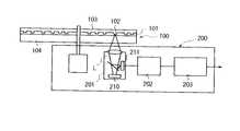
図28は、その装置を概略的に示すブロック図である。
【0003】
図28において、符号100がCDであり、符号200がプレーヤである。
CD100は、信号層101にディジタル情報としてのピット102が凹設されており、この信号層101の上面と下面とに、保護層103と透明プラスチック基板104とが貼り付けられている。
【0004】
このようなCD100においては、トラックピッチが1.6μm、最短ピット長が0.9μmに設定されている。
プレーヤ200は、ピット102の有無を検出して、CD100の情報を再生する装置であり、光ピックアップ201と、RFアンプ202と、ディジタル信号処理回路203等を備えている。
【0005】
すなわち、光ピックアップ201のレーザダイオード210から波長780nmのレーザ光LをCD100側に照射し、反射してきたレーザ光Lをフォトダイオード211で検出する。そして、そのRF信号をRFアンプ202で増幅した後、ディジタル信号処理回路203でディジタル処理等して、CD100の情報を再生するようになっている。
【0006】
しかし、上記したCD100およびそのプレーヤ200では、レーザ光Lを使用して、CD100のピット102を光学的に検知する構造となっているので、その光の波長の限界があり、検知精度が低い。このため、ピット102の大きさを小さくすることができず、CD100に多量の情報量を記録することができない。たとえば、直径12cmのCD100では、記録可能なディジタル情報量は、650メガバイト程度である。
【0007】
また、他の記録媒体およびその情報再生装置として、最近話題のDVD(Digital Video Disk)およびそのプレーヤがある。
この装置は、DVDのトラックピッチを0.84μm、最短ピット長を0.451μmに設定し、波長が635nm以内のレーザ光でピットの有無を検出することができるようになっている。したがって、CD100に比べて、高密度で多量の情報をDVDに記録することができる。しかしながら、それでも、直径12cmのDVDに記録可能なディジタル情報は、3.9ギガバイト程度である。
【0008】
これに対して、波長が青色レーザのレーザ光を用い、CDやDVDの情報を検知すると、検知精度は向上する。しかし、光を用いてピットを検出する以上、そこには限界があり、せいぜい、0.45μm〜0.3μm程度の大きさのものしか検知することができない。
【0009】
したがって、CDやDVD等、従来の記録媒体およびその情報再生装置では、動画情報や音声情報等、多量の情報を記録、再生することが要求されるマルチメディア用の機器として、不十分であった。
一方、半導体の不揮発性メモリのように記録再生ができる記録媒体及びその情報記録再生装置としては、いわゆるミニディスクとそのプレーヤーがある。
【0010】
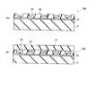
ミニディスクの記録媒体300は、光磁気ディスクであり、図29に示すように、ポリカーボネート基板301にコルゲート状に磁性層302が形成され、その磁性層302の上に保護層303が設けられた構造を有する。
記録するときは、外部磁界をかけながらレーザー光を当てて熱を加え、磁化を反転させ、磁区の向きによって“1”“0”の情報を記録する。そして、再生するときは、磁性層の磁化の向きに対応して、レーザーの反射光の偏光面が、正、逆方向にわずかに回転する(カー効果)ことを利用し、レーザーを照射して、磁化の向きを読みとるものである。
【0011】
しかしながら、ミニディスクにおいても、光を感知媒体に用いているので、光の波長の限界に逆らえることはできず、図29に示すように、記録幅のピッチは、1.1μm+0.5μmで、約1.6μmである。
本発明は、上述した課題を解決するためになされたもので、情報の大容量化と情報読取の高精度化とを可能にしたROM記録媒体、及び不揮発性メモリとして機能する記録媒体、並びにそれらの情報再生装置、情報記録装置及び情報記録再生装置を提供することを目的としている。
【0012】
上記目的を達成するため、本発明の記録媒体は、電子を保持することによって情報を記録可能な記録媒体であって、基板と、前記基板に形成された導電層と、前記導電層に積層された絶縁層と、周囲から電気的に絶縁されるように前記絶縁層に形成された固定電極とを有し、前記固定電極は、前記電子を保持し、前記導電層は、電圧が印加されることによって前記固定電極が保持する前記電子を放電させて前記情報を消去する。
【0013】
上記目的を達成するため、本発明の情報記録装置は、導電層と、前記導電層に形成された絶縁層と、周囲から電気的に絶縁されるように前記絶縁層に形成され、電子を保持する固定電極とを有する記録媒体に情報を記録する情報記録装置であって、前記記録媒体の前記固定電極に電子を注入することによって前記情報を記録させる電子銃を有する。
【0014】
上記目的を達成するため、本発明の情報再生装置は、導電層と、前記導電層に形成された絶縁層と、周囲から電気的に絶縁されるように前記絶縁層に形成され、電子を保持する固定電極とを有する記録媒体に記録された情報を再生する情報再生装置であって、前記固定電極に対向することによりコンデンサを構成する対向電極と、前記固定電極と前記対向電極との間の静電容量の変化を検出する検知器と、前記検知器の検知結果に基づいて、前記情報を再生する再生回路とを有する。
【0015】
上記目的を達成するため、本発明の情報記録再生装置は、導電層と、前記導電層に形成された絶縁層と、周囲から電気的に絶縁されるように前記絶縁層に形成され、電子を保持する固定電極とを有する記録媒体に情報を記録すると共に、前記記憶媒体に記録された情報を再生する情報記録再生装置であって、前記記録媒体の前記固定電極に電子を注入し保持させることによって前記情報を記録させる電子銃と、前記固定電極に対向することによりコンデンサを構成する対向電極と、前記固定電極と前記対向電極との間の静電容量の変化を検出する検知器と、前記検知器の検知結果に基づいて、前記情報を再生する再生回路とを有する。
【0030】
【発明の実施の形態】
以下、本発明の実施形態について図面を参照して説明する。
(第1および第2発明の実施形態)
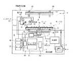
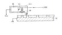
図1は、第1および第2発明の一実施形態に係る記録媒体およびその情報再生装置を示す概略図である。
【0031】
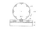
本実施形態の情報再生装置は、ディスク1(記録媒体)を収納する収納室Aと種々の機器を収納した機器室Bとに区画されている。
そして、機器室Bに、収納室A内を真空にする真空ポンプ2が取り付けられ、収納室Aと機器室Bとに、ディスク1の保護板13を取り出しおよび取り付けるためのディスク搬送機構3が組み付けられている。また、収納室Aには、ディスク1の情報読取を行うピックアップ4−1が装着されている。さらに、機器室Bには、ピックアップ4−1で読み取られた情報を再生する再生回路5と、真空ポンプ2やディスク搬送機構3を制御すると共にディスク1の信号層12に所定電圧VDDを印加する制御部6とが設けられている。
【0032】
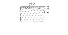
ディスク1は、図2に示すように、中心部に軸孔10を有した直径12cmの大きさの円板体であり、基板11と信号層12と保護板13との三構造になっている。
具体的には、基板11は、下面(図2下側面)にラベル等が貼り付け可能であり、その厚さは、1000μm〜1200μmに設定されている。
【0033】
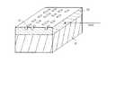
信号層12は、厚さが1μmのアルミニウムで形成されており、基板11の上にコーティングされている。そして、信号層12の上面側には、図3および図4に示すように、複数のピット14がトラックに沿って凹設されている。なお、基板11をアルミニウムで構成し、信号層12を省略することも可能である。
【0034】
ピット14は、信号層12の所要箇所をプレスして、表面を凹ませることにより形成されている。ここで、信号層12が柔らかいアルミニウムであるので、プレス作業によって、ピット14を容易且つ高精度で形成することができる。すなわち、信号層12をアルミニウム製にすることで、製作作業工数と製品コストの低減化を図っている。
【0035】
保護板13は、信号層12のピット14等にゴミが侵入するのを防止するための薄いアルミニウム板であり、信号層12の上面に真空チャックされている。
すなわち、信号層12のピット14内を真空にし、保護板13を信号層12に吸着させた状態にしておくことで、ディスク1の保存時における損傷の防止と、使用時における保護板13の取り外しとを容易にしている。
【0036】
このようなディスク1は、図1に示す情報再生装置のディスク挿入/引抜口9を介して、収納室A内に挿入することができるようになっている。
真空ポンプ2は、ディスク1の挿入時に、制御部6の制御で作動し、収納室A内の空気を装置外部に排出して、収納室A内を真空にするポンプである。また、この真空ポンプ2は、ディスク1の引抜時に、逆作動して、装置外部の空気を収納室A内に送り込むように、制御部6によって制御される。
【0037】
ディスク搬送機構3は、ディスク1の保護板13の取外および取付を行い、また、サーボ71で制御されるモータ7の回転軸70にディスク1を装着する機構であり、収納室Aの上面に取り付けられた固定吸着アーム30と、アクチュエータ31で上下動される可動吸着アーム32とを有している。
【0038】
具体的には、固定吸着アーム30および可動吸着アーム32は、その先端にゴム等の可撓性素材で形成された吸盤を有している。またアクチュエータ31は、制御部6の制御によって、ディスク1の挿入後で真空ポンプ2の作動終了時に、可動吸着アーム32を上昇させた後、下降させるように作動する。また、このアクチュエータ31は、ディスク1の引抜時に、可動吸着アーム32を上昇させ、真空ポンプ2の逆作動終了時に、可動吸着アーム32を下降させるように作動する。
【0039】
このようなディスク搬送機構3によって搬送されるディスク1の情報を読み取るためのピックアップ4−1は、電子銃40と検知器42とを備えている。
電子銃40は、ディスク1の信号層12の所定箇所に、電子線Eを打ち出すための機器であり、電子線Eは、電子銃40の出力側に配置された集束コイル41によって、集束されるようになっている。
【0040】
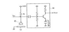
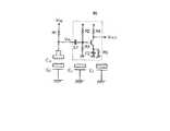
検知器42は、信号層12から反射してきた電子線Eを捉えて、その強弱を検知する機器である。
図5は、この検知器42を示す回路図である。
図5に示すように、この検知器42は、ディスク1の信号層12で反射した電子線Eの電子を捉えるアルミニウム等の金属箔43と、出力電圧生成回路44とを有している。
【0041】
具体的には、金属箔43には、負荷R1を介して制御部6からの電圧VDDが印加されている。
また、出力電圧生成回路44は、金属箔43と負荷R1との接続点に入力端が接続された直流除去用のコンデンサC1を有している。そして、このコンデンサC1の出力端に、トランジスタQの動作電圧を確保するためのバイアス用抵抗R2,R3の接続点が接続されている。そして、この抵抗R2,R3の接続点には、トランジスタQのベースが接続されている。このトランジスタQのコレクタは、抵抗R4を介して電圧VDDに接続され、エミッタは、並列なバイパスコンデンサC2と抵抗R5とに接続されている。
【0042】
これにより、金属箔43が電子線Eを捉えると、電子線Eに対応した入力電圧Vinが生じ、この入力電圧VinがトランジスタQによって、デルタ関数状の電圧パルスである出力電圧Voutに変換されるようになっている。
このような検知器42と電子銃40とを有したピックアップ4−1の動きは、図1に示すトラッキング用およびフォーカス用のサーボ49によって制御されるようになっている。
【0043】
再生回路5は、CDのプレーヤ等で用いられている周知の回路であり、RFアンプ50、ディジタル信号処理部51、D/A変換部52等を備え、ピックアップ4−1からの出力電圧Voutに基づいて、ディスク1の情報を再生する。
次に、本実施形態の情報再生装置が示す動作について説明する。
【0044】
図1に示すように、保護板13側を上にしたディスク1を収納室A内に挿入すると、真空ポンプ2が作動し、収納室A内の空気が装置外部に排出されて、収納室A内が真空になる。
すると、ディスク搬送機構3のアクチュエータ31が作動し、可動吸着アーム32が上昇して、ディスク1の上面を固定吸着アーム30が押し付ける。これにより、ディスク1の基板11が可動吸着アーム32に吸着され、保護板13が固定吸着アーム30に吸着された状態となる。しかる後、アクチュエータ31が逆作動し、可動吸着アーム32が下降する。この結果、実線で示すように、固定吸着アーム30に吸着された保護板13が信号層12から剥がされ、信号層12を露出させたディスク1がモータ7の回転軸70に嵌められる。
【0045】
この状態で、再生回路5を作動させると、ディスク1が回転すると共に、ピックアップ4−1がディスク1上の所定位置まで移動し、信号層12に電圧VDDが印加された状態で、ピックアップ4−1による走査が行われる。
すなわち、ピックアップ4−1の電子銃40が、ディスク1のトラックに沿って、信号層12に電子線Eを打ち出す。この電子線Eは、集束コイル41によって、集束され、電圧VDDによって正極となった信号層12に効率良く当たる。
【0046】
このとき、電子線Eが信号層12の凹状のピット14に当たると、電子線Eはピット14で散乱されるので、電子線Eは、検知器42によってほとんど検知されない。逆に、電子線Eがピット14以外の平面部分に当たると、電子線Eは検知器42方向に反射されるので、電子線Eは、検知器42で検知される。
【0047】
したがって、電子銃40で信号層12のトラックに沿って走査して行くと、ピット14の有無によって、図5に示す金属箔43に捉えられる電子線Eの電子量が増減するので、入力電圧Vinがそれに応じて変化する。
具体的には、図6の(a)に示すように、ピット14部分の走査では、入力電圧Vinがほぼ一定電圧を保持し、ピット14以外の平面部分を走査すると、入力電圧Vinに大きな立上り部aが生じる。したがって、たとえば、平面部分を二値の「0」、ピット14を「1」と設定しておくことで、信号層12に記録されている二値化ディジタル信号が電子銃40および検知器42の作用によって読み取られ、その内容を示す入力電圧Vinが出力電圧生成回路44に入力される。
【0048】
出力電圧生成回路44に入力された入力電圧Vinは、トランジスタQによって増幅変換される。この結果、図6の(b)に示すように、入力電圧Vinの立上り部aに対応した極めて低レベルの電圧パルスbを有した出力電圧Voutが、出力電圧生成回路44から再生回路5へと出力され、再生回路5によって、音声再生または画像再生される。
【0049】
再生が終了すると、図1に示すディスク搬送機構3の可動吸着アーム32が上昇し、ディスク1を持上げて、固定吸着アーム30に吸着されている保護板13と信号層12とを合致させる。これと同時に、真空ポンプ2が逆作動し、装置外部の空気が収納室A内に送り込まれる。この結果、収納室A内が正圧状態になり、ピット14内のみが真空状態になるので、保護板13が信号層12に吸着され、ディスク1が挿入前の状態に復元される。この状態で、ディスク1を収納室Aから引き抜いて保存する。
【0050】
このように、本実施形態によれば、走査電子顕微鏡のように、電子銃40から電子線Eをディスク1の信号層12に打ちながら走査して、信号層12に記録された情報を読み取る構造であるので、次のような効果を得ることができる。
すなわち、電子線Eによる検出精度は、図14に示したCDのようにレーザ光Lによる検出精度に比べると、2桁以上も検出精度が高い。したがって、ディスク1の信号層12に形成するピット14の大きさを非常に小さくすることができる。この結果、従来のCDやDVDに比べると、桁単位で大きい情報を記録することができるディスク1を提供することができ、しかも、その情報を高速で読み取ることができる。
【0051】
また、ピックアップ4−1による読取動作の原理は、上記したように、走査電子顕微鏡とほぼ同様であるが、ピックアップ4−1では、電子顕微鏡のように、対物コイル、接眼コイル、偏極板等を必要としないので、構造が簡単になり、その分、電子顕微鏡に比べて、製造コストを低く抑えることができる。さらに、ピックアップ4−1とディスク1との距離はほぼ一定であり、このため、電子銃40の電子線Eの強度が小さくて済み、この結果、電力消費の低減化と装置の長寿命化とを図ることができる。
【0052】
図7は、ピックアップ4−1に適用された検知器の変形例を示す回路図である。
この検知器は、出力電圧生成回路44のコンデンサC1の入力端に、ダイオードDを接続して、接地した構造となっている。具体的には、ダイオードDのN層のコンデンサC1の入力端に接続され、P層が接地されている。
【0053】
これにより、電圧VDDに雷等の高電圧がかかったときに、多量の電子をN層に流して、このダイオードDが保護ダイオードとして機能するようになっている。また、N層とP層間の容量によって、コンデンサC1以降の回路の容量とのカップリング調整を図ることができるようになっている。
【0054】
なお、本発明は、上記実施形態に限定されるものではなく、発明の要旨の範囲内において種々の変形や変更が可能である。
たとえば、本実施形態では、信号層11および基板12をアルミニウムで形成したが、金属であるならば、これに限るものではなく、プレスの容易なチタン合金等をも用いることができる。
【0055】
また、本実施形態では、ディスク1挿入時に収納室Aを真空にしたが、読取精度の許容範囲で、収納室Aの真空度を弱くすることができる。
(第3発明の実施形態)
次いで、第3発明の一実施形態に係る情報再生装置について説明する。
【0056】
図8は、本実施形態の要部を示す概略図である。なお、図1ないし図7の部材と同一部材については、同一符号を付して説明する。
本実施形態のピックアップ4−2には、制御部6から5ボルトの電圧VDDが印加された金属体45が設けられている。そして、この金属体45には、図8および図9に示すように、検知回路としての出力電圧生成回路44が接続されている。また、ディスク1の信号層12は接地されており、この信号層12に金属体45を対向近接させた状態で、ピックアップ4−2を走査するようになっている。
【0057】
これにより、金属体45がピット14以外の平面部分に至ると、金属体45と信号層12との距離が著しく短くなるので、金属体45と信号層12との間で、放電が発生する。したがって、金属体45で信号層12のトラックに沿って走査して行くと、ピット14の有無によって、放電が生じたり、生じなかったりする。この結果、図10の(a)に示すように、ピット14部分の走査では、入力電圧Vinがほぼ電圧VDDを保持し、ピット14以外の平面部分を走査すると、入力電圧Vinに大きな立下り部cが生じる。
【0058】
そして、この入力電圧Vinが出力電圧生成回路44に入力されると、トランジスタQによって増幅変換され、図10の(b)に示すように、立下り部cに対応した極めて高レベルの電圧パルスdを有した出力電圧Voutが出力される。この出力Voutは、出力電圧生成回路44から再生回路5に入力される。
【0059】
このように、本実施形態の情報再生装置によれば、電子銃や集束コイル等を用いず、金属体45のみでピット14の有無を検出することができるので、構造が簡単になり、この結果、製造作業工数と製品コストをさらに低減化することができる。
【0060】
この他の構成、作用効果は上記第1および第2発明の実施形態と同様であるので、その記載は省略する。
(第3発明の他の実施形態)
次に、第3発明の他の実施形態に係る情報再生装置について説明する。
【0061】
図11は、本実施形態の要部を示す概略図である。なお、図8の部材と同一部材については、同一符号を付して説明する。
本実施形態のピックアップ4−3は、電圧VDDが印加された金属体45に、検知回路としての出力電圧生成回路46が接続されている。しかし、このピックアップ4−3は、金属体45を信号層12に対して放電しない距離だけ離した状態で、信号層12のトラックに沿って走査するようになっている。
【0062】
したがって、金属体45と信号層12とは、ピット14の有無によって静電容量が変化する可変コンデンサとして機能するようになっている。このため、出力電圧生成回路46は、図12に示すように、上記出力電圧生成回路44からコンデンサC1を取り除いた構造となっている。
【0063】
このような構成により、金属体45がピット14以外の平面部分に至ると、金属体45と信号層12との距離が短くなるので、静電容量が増大する。したがって、金属体45で信号層12のトラックに沿って走査して行くと、ピット14の有無によって、金属体45と信号層12で構成されるコンデンサの静電容量が大きくなったり、小さくなったりする。この結果、図13の(a)に示すように、ピット14部分の走査では、入力電圧Vinがほぼ電圧VDDを保持し、ピット14以外の平面部分を走査すると、入力電圧Vinに小さな立下り部eが生じる。
【0064】
そして、この入力電圧Vinが出力電圧生成回路46に入力されると、トランジスタQによって増幅変換され、図13の(b)に示すように、立下り部eに対応したレベルの電圧パルスfを有した出力電圧Voutが出力される。この出力電圧Voutは、出力電圧生成回路46から再生回路5に入力される。
【0065】
このように、本実施形態の情報再生装置によれば、放電現象を用いず、金属体45と信号層12との間の容量変化でピット14の有無を検出することができるので、金属体45や信号層12の耐久性の向上を図ることができる。
その他の構成、作用効果は上記実施形態と同様であるので、その記載は省略する。
(第4発明の実施形態)
第1発明〜第3発明にかかる記録媒体は、読み出し専用の記録媒体(ROM)であったが、以下の実施形態の記録媒体は、半導体メモリのいわゆるフラッシュメモリに相当する不揮発性メモリとして機能する記録媒体である。
【0066】
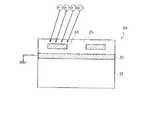
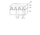
この第2記録媒体20は、例えば図14、図15に示すように、基板21の上にアルミニウムなどの金属などで構成される導電層22が設けられ、この導電層22の上には酸化シリコンなどで構成される絶縁層23が設けられ、更に、この絶縁層の上には、図15(B)に示すように、トラックに沿って所定のピッチでアルミニウムなどの金属で構成される固定電極24が島状に形成されており、これらの固定電極24は、保護絶縁層25で被覆された構造を有する。
【0067】
この構造においては、それぞれの固定電極24は、図15(A)に示すように、絶縁層23と保護絶縁層25とに被覆されて、周囲から絶縁されている。固定電極24の長さは、0.01μm、すなわち100Å程度にすることができる。これは、光を媒体としたDVD等の限度が0.3μm程度であるのに比べて、数百倍の記録密度が可能であることを示す。
【0068】
この記録媒体20に書き込むときは、図16に示すように、真空中で、導電層22をGNDに設定し、電子銃などをスキャンさせながら電子を所定の固定電極24に保護絶縁層25を通して打ち込み、マイナスに帯電させて、情報の蓄積を行う。これにより、図17に示すように、固定電極24は、その下の導電層22(GND)との間の容量C0に帯電することになる。上記電子銃で電子を固定電極24に打ち込む際、固定電極24に打ち込まれなかった電子は、GNDに設定された下層の導電層22に吸収され、絶縁膜23、25の電子帯電を防止することができる。
【0069】
このように、固定電極24に注入された電子は、固定電極24が周囲から絶縁されているので、半導体メモリのEEPROM(Electrically Erasable Programmable ROM)のフローティングゲートのように、そのまま電子を保持し、不揮発性メモリとして機能する。
【0070】
また、固定電極に注入された電子を放電させて、情報を消去するには、次の2つの方法が考えられる。まず第1に、図18(A)に示すように、固定電極24の下の導電層22の電圧をVDDに上げることにより、固定電極24の電子を導電層22に吸い取ることができ、これによりフラッシュメモリのように一括消去することができる。この電子の吸い取りは、フラッシュメモリのF−N電流と同じ原理で、絶縁膜を通過するトンネル電流によって行われる。このため、この消去方法を採用する場合、固定電極24と導電層22を隔てている絶縁層23の厚さは薄くする。
【0071】
もう一つの消去方法は、図18(B)に示すように、消去ヘッドとしての導電板80を記録媒体20の表面に密着させ、この導電板80にVDDを印加することにより、固定電極24の電子を導電板80に吸い取ることができる。この場合は、導電層22と固定電極24を隔てている絶縁層23の厚さを薄くする必要がない。
【0072】
また、読み出しは、第3発明の他の実施形態と同様に、静電容量の変化を検知することにより行うことができる。この検知機構について、図19〜図21で説明する。なお、図11の部材と同一部材については、同一符号を付して説明する。
【0073】
図19に示すように、ピックアップ4を構成する対向電極45−1は、電圧VDDが印加され、検知回路としての出力電圧生成回路46が接続されている。このピックアップ4は、対向電極45−1を固定電極24のトラックに沿って走査するようになっている。なお、図面では、対向電極24は記録媒体20の表面から離間した状態としているが、対向電極45−1の面を記録媒体20の表面に密着させていても良い。
【0074】
対向電極45−1を固定電極24に近接させると、近接効果により、図19に示すように、固定電極24と対向電極45−1との間には近接静電効果(容量結合)が生じる。この概念図を図20に示す。
このような構成により、対向電極45−1が帯電した固定電極24と対向しているときには、対向電極45−1が帯電していない固定電極24と対向しているときと比較して静電容量が増大する。したがって、対向電極45−1で固定電極24のトラックに沿って走査して行くと、固定電極24の帯電の有無によって、固定電極24と対向電極45−1で構成されるコンデンサの静電容量が大きくなったり、小さくなったりする。この結果、図21(a)に示すように、帯電していない固定電極24の走査では、入力電圧Vinがほぼ電圧VDDを保持し、帯電した固定電極24と近接すると、入力電圧Vinに小さな立下り部gが生じる。
【0075】
そして、この入力電圧Vinが、例えば図20に示すような出力電圧生成回路46に入力されると、トランジスタQによって増幅変換され、図21(b)に示すように、立下り部gに対応したレベルの電圧パルスhを有する出力電圧Voutが出力される。この出力電圧Voutは、出力電圧生成回路46から再生回路に入力される。
【0076】
このように、本記録媒体は、電子を感知媒体に用いているため、光の波長の限界を超えた多量の情報の書き込み読込が可能である。固定電極に電子を注入することにより書き込みができ、そして、一括消去できるため、半導体のフラッシュメモリと同様の不揮発性メモリとして機能する。半導体のフラッシュメモリにおいては、X−Y平面にX−デコーダー回路/Y−デコーダー回路を装備し、マトリックス状に配置されたメモリセルを電気的に任意選択するが、本記録媒体では、例えばディスクの回転と半径方向の位置移動(一般的には、電子銃と対向電極を装備したピックアップの直接的なメカニカルな位置移動)により特定するものである。
【0077】
この場合、書き込み、読み出し、消去は、記録媒体の物理的な形状に変化を与えないので、書き込み、読み出し、消去の回数に制限はない。
このような記録媒体の製造方法は、例えば基板21を樹脂などで円盤状に成形し、この円盤状基板21に蒸着などでアルミニウムなどの金属を堆積して導電層22を形成する。次に、CVD法などで例えば酸化シリコンなどの絶縁層を堆積する。この絶縁層22にプレスなどで固定電極用の凹部を型押しし、この凹部にアルミニウムなどの溶融金属を流し込み、凹部を金属で埋め、固定電極を形成する。その後、CVD等で酸化シリコンなどの保護絶縁層を形成し、固定電極を絶縁層で被覆し、本記録媒体を製造することができる。
(第5〜7発明の実施形態)
次に、上記不揮発性メモリとして機能する記録媒体の情報記録装置と情報再生装置を兼備した情報記録再生装置の一例について図22で説明する。
【0078】
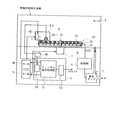
この情報記録再生装置は、円盤状の記録媒体20を収納する収納室Aと種々の機器を収納した機器室Bとに区画されている。機器室Bに、収納室A内を真空にする真空ポンプ2が取り付けられ、収納室Aには、記録媒体20に書き込み、読み出しを行うピックアップ4−4と記録媒体を装着させる回転ディスク70が設けられている。さらに、機器室Bには、ピックアップ4−4で情報の書き込みを行うと共に、読み取られた情報を再生する処理回路5と、真空ポンプ2を制御すると共に記録媒体20の導電層22に所定電圧VDDを印加する制御部6とが設けられている。
真空ポンプ2は、記録媒体20の挿入時に、制御部6の制御で作動し、収納室A内の空気を装置外部に排出して、収納室A内を真空にする。記録媒体を取り出すときは、制御部6の制御で収納室Aを大気圧に戻すようになっている。
【0079】
また、ピックアップ4−4は、電子銃40と対向電極45−1とを備えている。なお、電子銃と対向電極とをそれぞれ別のピックアップを構成するようにしても良い。
電子銃40は、ディジタル信号処理部51で所定の固定電極に電子線を打ち出すように制御される。
【0080】
対向電極45−1には、図19、図20に示したように、電圧VDDが印加され、また、検知回路としての出力電圧生成回路46が接続されている。この出力電圧生成回路46は、図20に一例を示したように、対向電極45−1と負荷R1との接続点に入力端が接続された直流除去用のコンデンサC1を有している。このコンデンサC1の出力端に、トランジスタQの動作電圧を確保するためのバイアス用抵抗R2,R3の接続点が接続されている。そして、この抵抗R2,R3の接続点には、トランジスタQのベースが接続されている。このトランジスタQのコレクタは、抵抗R4を介して電圧VDDに接続され、エミッタは、並列なバイパスコンデンサC2と抵抗R5とに接続されている。
【0081】
これにより、対向電極からの入力電圧VinがトランジスタQによって、デルタ関数状の電圧パルスである出力電圧Voutに変換されるようになっている。このような電子銃40と対向電極45−1を備えるピックアップ4−4の動きは、図22に示すトラッキング用およびフォーカス用のサーボ49によって制御されるようになっている。
【0082】
また、回転ディスク70は、サーボ71により制御されるモータ7で回転される。そして、回転ディスクに装着される記録媒体20の導電層22には、必要により制御部6からVDDが印加されるようになっている。
処理回路5は、RFアンプ50、ディジタル信号処理部51、D/A変換部52等を備え、ピックアップ4−4の電子銃での電子の注入の制御、及び出力電圧生成回路を介して対向電極45−1からの出力電圧Voutに基づいて、記録媒体20の情報を再生する。
【0083】
このような情報記録再生装置における書き込み操作について説明すると、記録媒体20を装置内の回転ディスク70に装着すると、真空ポンプ2が作動して、収納室A内が真空にされる。そして、記録媒体20の導電層22に電圧VDDが印加される。これにより、図18(A)に示すような記録の一括消去が行われる。
【0084】
次に、処理回路5が作動して回転ディスク70が回転すると共に、ピックアップ4−4が記録媒体20の所定位置まで移動する。次いで、ピックアップ4−4が、記録媒体20の半径方向に移動しつつ、トラックに沿って固定電極24を走査しながら、処理回路5の制御で電子銃40から所定の固定電極24に電子を打ち込む。書き込みが終了した後、制御部6の制御で収納室A内が大気圧に戻され、記録媒体20を情報処理装置から取り出せる状態となる。
【0085】
また、読み出し操作は、情報を記録した記録媒体20を回転ディスク70に装着した後、処理回路5が作動して回転ディスク70が回転すると共に、ピックアップ4−4が記録媒体20の所定位置まで移動する。次いで、ピックアップ4−4が、記録媒体20の半径方向に移動しつつ、対向電極45−1が固定電極24を走査しながら、図19〜図21に示したように、書き込まれた情報を読み出す。
【0086】
このように本情報記録再生装置は、上記記録媒体20の情報の書き込み、消去、読み出しを1台で行える構成となっている。勿論、情報の書き込みと消去を行う情報記録装置と情報の読み出しを行う情報再生装置とを別々に構成しても良い。
【0087】
次に、上記記録媒体及び情報再生装置の変形について説明する。図23は、基板21を例えばアルミニウムなどの導電性の材料で構成し、図14に示した記録媒体20の導電層22を省略し、基板21と導電層22を兼用した構造の記録媒体20aを示す。これにより、単純化した構造となり、コストの低減が可能となる。
【0088】
また、図24は、基板21の上に積層した導電層22に更に絶縁層26を設け、この絶縁層26に形成した凹部に固定電極24を絶縁層26の表面からわずかに凹むように埋め込んだ構造の記録媒体20bである。この構造では、固定電極24の表面は露出しているので、固定電極24に注入した電子が時間の経過と共に、固定電極24の露出面から放電するおそれがある。このため、固定電極24の露出面は、真空状態として絶縁する必要がある。そのため、保護板27が必要となり、図1に示したような装置を用いて真空中で保護板27を記録媒体20bの上に被せ、図24(B)に示すように、固定電極24と保護板27との間の空隙28の真空を利用して大気圧で保護板27を記録媒体20bに吸着させ、固定電極24の露出面を真空と接触させて固定電極24を周囲から絶縁する必要がある。書き込み、再生をするときには、図1に示したような装置を用いて、真空中で保護板27を剥離させて行う。したがって、真空中で保管するときには、このような保護板27は必要ではない。
【0089】
図25に示す記録媒体20cは、基板21の上の導電層22と、その導電層22の上に積層された絶縁層23の上に、固定電極24がトラックに沿ってブロック状に固着した構造である。この構造の記録媒体21cの保存方法は、固定電極24を真空中で保存する必要があるので、同図に示すように、保存時には真空中で被せた保護板27cを記録媒体20cに吸着させておく。
【0090】
また、図26に示す記録媒体20dは、固定電極24とその下の絶縁層23dとを同一形状の積層体として導電層22の上にトラックに沿って配置した構造となっている。この構造の利点は、電子銃40で電子を固定電極24に注入する際に、固定電極24に注入されなかった電子が直接導電層22に取り込まれ、絶縁層23aの電子帯電を可及的に防止できることである。その他は、保存時には真空中で保管するために保護板27dを必要とするなど、図25に示す記録媒体21cと同様である。
【0091】
これらの記録媒体20c、20dの一括消去は、固定電極24が記録媒体21c、21dの表面から突出しているので、例えば金属板を固定電極24に密着させることにより、その金属板の電圧(V0)に固定電極24を瞬間的にチャージさせることができる。この場合、金属板は、単に接触するだけでよいので、固定電極24を破損させるおそれは少ない。その他の電子の注入、書き出しは、上記と同様にできる。
【0092】
また、これらの記録媒体21c、21dのような固定電極24が記録媒体表面から突出している構造においては、破壊読み出しも可能である。すなわち、対向電極45−1を固定電極24と接触させ、直接固定電極24の電子を対向電極45−1に吸い上げ、その際、検知した「1」又は「0」の情報を順次、再度書き込む手法で情報を保存することができる。
【0093】
図27は、再生用のピックアップの変形例を示すもので、記録媒体のトラックの幅とほぼ同一の幅の車輪に複数の対向電極を固定電極のピッチと同じピッチで埋め込んだ構造のピックアップ4−5を用いる。再生するときは、このピックアップをトラックに沿って転がして走査し、対向電極45−1と固定電極24とを正確に対向させるものである。この場合、記録媒体の表面には、例えばタングステンなどでレール状のものをトラック間に作っておき、車輪状ピックアップが正確にトラックをいわばトロッコのように転がることができるようにしておくことができる。
【0094】
【発明の効果】
以上のように、本発明は、情報の大容量化と情報読取の高精度化とを可能にした記録媒体、並びにそれらの情報再生装置、情報記録装置及び情報記録再生装置を提供することができる。
【図面の簡単な説明】
【図1】第1および第2発明の一実施形態に係る記録媒体およびその情報再生装置を示す概略図である。
【図2】図1の記録媒体を示す斜視図である。
【図3】図2の記録媒体の部分断面図である。
【図4】図2の記録媒体のピットの構造と電圧印加状態を一部破断して示す斜視図である。
【図5】図1の検知器を示す回路図である。
【図6】図5の検知器による読取時の信号波形図であり、図6の(a)は入力信号を示し、図6の(b)は出力信号を示す。
【図7】図1の検知器の変形例を示す回路図である。
【図8】第3発明の一実施形態に係る情報再生装置の要部を示す概略図である。
【図9】図8のピックアップの出力電圧生成回路を示す回路図である。
【図10】図8のピックアップによる読取時の信号波形図であり、図10の(a)は入力信号を示し、図10の(b)は出力信号を示す。
【図11】第3発明の他の実施形態の要部を示す概略図である。
【図12】図11のピックアップの出力電圧生成回路を示す回路図である。
【図13】図11のピックアップによる読取時の信号波形図であり、図13の(a)の入力信号を示し、図13の(b)は出力信号を示す。
【図14】第4発明の記録媒体の一例を示す部分断面図である。
【図15】第4発明の記録媒体を示すもので、(A)は断面図、(B)は平面図である。
【図16】第4発明の記録媒体に書き込む様子を説明する概念図である。
【図17】第4発明の記録媒体に書き込む状態を説明する概念図である。
【図18】(A)、(B)は、第4発明の記録媒体のそれぞれ一括消去を説明する概念図である。
【図19】第4発明の記録媒体の読み出しを行う状態を説明する概念図である。
【図20】第4発明の記録媒体の読み出しを行う状態を説明する概念図である。
【図21】図19のピックアップによる読取時の信号波形図であり、(a)は入力信号を示し、(b)は出力信号を示す。
【図22】第7発明の情報記録再生装置の構成を示す概略図である。
【図23】第4発明の記録媒体の変形例を示す断面図である。
【図24】第4発明の記録媒体の他の変形例を示すもので、(A)は記録媒体、(B)は保護板を被せた状態を示すそれぞれ断面図である。
【図25】第4発明の記録媒体の更に他の変形例を示す断面図である。
【図26】大発明の記録媒体のまた更に他の変形例を示す断面図である。
【図27】再生用のピックアップの変形例を示す断面図である。
【図28】従来例に係る記録媒体およびその情報再生装置を示すブロック図である。
【図29】いわゆるミニディスクの断面構造を示す断面図である。
【符号の説明】
1 ディスク
5 再生回路
11 基板
12 信号層
13 保護板
14 ピット
40 電子銃
42 検知器
20 記録媒体
21 基板
22 導電層
23 絶縁層
24 固定電極
25 保護絶縁層
45−1 対向電極[0001]
BACKGROUND OF THE INVENTION
The present invention relates to a recording medium that records digital information, a recording medium that functions as a nonvolatile memory, an information reproducing apparatus, an information recording apparatus, and an information recording / reproducing apparatus.
[0002]
[Prior art and problems to be solved by the invention]
Conventionally, a ROM (Read Only Memory) recording medium for digital information and an information reproducing apparatus thereof include a CD (Compact Disk) and its player.
FIG. 28 is a block diagram schematically showing the apparatus.
[0003]
In FIG. 28,
In the
[0004]
In such a
The
[0005]
That is, a laser beam L having a wavelength of 780 nm is emitted from the
[0006]
However, since the
[0007]
As other recording media and information reproducing apparatuses there are recently-discussed DVDs (Digital Video Disks) and their players.
In this apparatus, the track pitch of DVD is set to 0.84 μm, the shortest pit length is set to 0.451 μm, and the presence or absence of pits can be detected with a laser beam having a wavelength of 635 nm or less. Therefore, a larger amount of information can be recorded on the DVD than the
[0008]
On the other hand, detection accuracy is improved when information on CDs or DVDs is detected using laser light having a blue laser wavelength. However, as long as pits are detected using light, there is a limit, and only pits having a size of about 0.45 μm to 0.3 μm can be detected.
[0009]
Therefore, conventional recording media such as CDs and DVDs and information reproducing apparatuses thereof are insufficient as multimedia devices that are required to record and reproduce a large amount of information such as moving image information and audio information. .
On the other hand, as a recording medium capable of recording / reproducing such as a semiconductor non-volatile memory and an information recording / reproducing apparatus thereof, there are a so-called mini-disc and its player.
[0010]
A
When recording, a laser beam is applied while applying an external magnetic field, heat is applied, magnetization is reversed, and information of “1” and “0” is recorded according to the direction of the magnetic domain. And when reproducing, the laser beam is irradiated using the fact that the polarization plane of the reflected light of the laser rotates slightly in the forward and reverse directions (Kerr effect) according to the direction of magnetization of the magnetic layer. The direction of magnetization is read.
[0011]
However, even in the mini-disc, since light is used as a sensing medium, it is impossible to counter the limit of the wavelength of light. As shown in FIG. 29, the recording width pitch is 1.1 μm + 0.5 μm. About 1.6 μm.
The present invention has been made to solve the above-described problems, and includes a ROM recording medium capable of increasing the capacity of information and increasing the accuracy of information reading, a recording medium functioning as a nonvolatile memory, and those An information reproducing apparatus, an information recording apparatus, and an information recording / reproducing apparatus are provided.
[0012]
In order to achieve the above object, a recording medium of the present invention is a recording medium capable of recording information by holding electrons, and is laminated on a substrate, a conductive layer formed on the substrate, and the conductive layer.Absurd An edge layer and a fixed electrode formed on the insulating layer so as to be electrically insulated from the surroundings; the fixed electrode holds the electrons; and the conductive layer is applied with a voltage. To erase the information by discharging the electrons held by the fixed electrode.
[0013]
In order to achieve the above object, an information recording apparatus of the present invention is formed on a conductive layer, an insulating layer formed on the conductive layer, and the insulating layer so as to be electrically insulated from the surroundings, and holds electrons. An information recording apparatus for recording information on a recording medium having a fixed electrode that has an electron gun that records the information by injecting electrons into the fixed electrode of the recording medium.
[0014]
In order to achieve the above object, an information reproducing apparatus according to the present invention is formed on a conductive layer, an insulating layer formed on the conductive layer, and the insulating layer so as to be electrically insulated from the surroundings, and holds electrons. An information reproducing apparatus for reproducing information recorded on a recording medium having a fixed electrode, wherein a counter electrode constituting a capacitor by facing the fixed electrode, and between the fixed electrode and the counter electrode A detector for detecting a change in capacitance; and a reproducing circuit for reproducing the information based on a detection result of the detector.
[0015]
In order to achieve the above object, an information recording / reproducing apparatus of the present invention comprises a conductive layer, an insulating layer formed on the conductive layer, and an insulating layer formed on the insulating layer so as to be electrically insulated from the surroundings. An information recording / reproducing apparatus for recording information on a recording medium having a fixed electrode for holding and reproducing information recorded on the storage medium, injecting and holding electrons into the fixed electrode of the recording medium An electron gun that records the information by: a counter electrode that constitutes a capacitor by facing the fixed electrode; a detector that detects a change in capacitance between the fixed electrode and the counter electrode; And a reproducing circuit for reproducing the information based on the detection result of the detector.
[0030]
DETAILED DESCRIPTION OF THE INVENTION
Embodiments of the present invention will be described below with reference to the drawings.
(Embodiments of the first and second inventions)
FIG. 1 is a schematic diagram showing a recording medium and an information reproducing apparatus thereof according to one embodiment of the first and second inventions.
[0031]
The information reproducing apparatus according to the present embodiment is divided into a storage chamber A for storing the disc 1 (recording medium) and a device chamber B for storing various devices.
A
[0032]
As shown in FIG. 2, the
Specifically, the
[0033]
The
[0034]
The
[0035]
The
That is, the inside of the
[0036]
Such a
The
[0037]
The
[0038]
Specifically, the fixed
[0039]
The pickup 4-1 for reading information on the
The
[0040]
The
FIG. 5 is a circuit diagram showing the
As shown in FIG. 5, the
[0041]
Specifically, the voltage VDD from the control unit 6 is applied to the
The output
[0042]
Thus, when the
The movement of the pickup 4-1 having the
[0043]
The
Next, the operation shown by the information reproducing apparatus of this embodiment will be described.
[0044]
As shown in FIG. 1, when the
Then, the
[0045]
When the reproducing
That is, the
[0046]
At this time, when the electron beam E hits the
[0047]
Therefore, when the
Specifically, as shown in FIG. 6A, when the
[0048]
The input voltage Vin input to the output
[0049]
When the reproduction is completed, the
[0050]
As described above, according to the present embodiment, as in a scanning electron microscope, the
That is, the detection accuracy by the electron beam E is higher by two digits or more than the detection accuracy by the laser beam L as in the CD shown in FIG. Therefore, the size of the
[0051]
The principle of the reading operation by the pickup 4-1 is almost the same as that of the scanning electron microscope as described above. However, in the pickup 4-1, the objective coil, the eyepiece coil, the polarization plate, etc. Therefore, the structure is simplified, and the manufacturing cost can be reduced as compared with the electron microscope. Further, the distance between the pickup 4-1 and the
[0052]
FIG. 7 is a circuit diagram showing a modification of the detector applied to the pickup 4-1.
This detector has a structure in which a diode D is connected to the input terminal of the capacitor C1 of the output
[0053]
As a result, when a high voltage such as lightning is applied to the voltage VDD, a large amount of electrons flow through the N layer, and this diode D functions as a protective diode. In addition, the coupling between the capacitors after the capacitor C1 can be adjusted by the capacitance between the N layer and the P layer.
[0054]
In addition, this invention is not limited to the said embodiment, A various deformation | transformation and change are possible within the range of the summary of invention.
For example, in this embodiment, the
[0055]
In this embodiment, the storage chamber A is evacuated when the
(Embodiment of the third invention)
Next, an information reproducing apparatus according to an embodiment of the third invention will be described.
[0056]
FIG. 8 is a schematic view showing a main part of the present embodiment. The same members as those in FIGS. 1 to 7 are described with the same reference numerals.
The pickup 4-2 of the present embodiment is provided with a
[0057]
Thereby, when the
[0058]
When this input voltage Vin is input to the output
[0059]
As described above, according to the information reproducing apparatus of the present embodiment, since the presence or absence of the
[0060]
Other configurations and operational effects are the same as those of the first and second inventions, and the description thereof is omitted.
(Another embodiment of the third invention)
Next, an information reproducing apparatus according to another embodiment of the third invention will be described.
[0061]
FIG. 11 is a schematic view showing a main part of the present embodiment. In addition, about the same member as the member of FIG. 8, the same code | symbol is attached | subjected and demonstrated.
In the pickup 4-3 of the present embodiment, an output
[0062]
Therefore, the
[0063]
With such a configuration, when the
[0064]
When the input voltage Vin is input to the output
[0065]
As described above, according to the information reproducing apparatus of the present embodiment, the presence or absence of the
Since other configurations and operational effects are the same as those of the above-described embodiment, description thereof is omitted.
(Embodiment of 4th invention)
The recording medium according to the first to third inventions is a read-only recording medium (ROM), but the recording medium of the following embodiment functions as a non-volatile memory corresponding to a so-called flash memory of a semiconductor memory. It is a recording medium.
[0066]
In the
[0067]
In this structure, as shown in FIG. 15A, each fixed
[0068]
When writing to the
[0069]
In this way, the electrons injected into the fixed
[0070]
The following two methods are conceivable for erasing information by discharging electrons injected into the fixed electrode. First, as shown in FIG. 18A, by raising the voltage of the
[0071]
In another erasing method, as shown in FIG. 18B, a
[0072]
Further, the reading can be performed by detecting a change in capacitance, as in the other embodiments of the third invention. This detection mechanism will be described with reference to FIGS. In addition, about the same member as the member of FIG. 11, the same code | symbol is attached | subjected and demonstrated.
[0073]
As shown in FIG. 19, a voltage VDD is applied to the counter electrode 45-1 constituting the pickup 4, and an output
[0074]
When the counter electrode 45-1 is brought close to the fixed
With such a configuration, when the counter electrode 45-1 is opposed to the charged fixed
[0075]
When this input voltage Vin is input to an output
[0076]
As described above, since the present recording medium uses electrons as the sensing medium, a large amount of information exceeding the limit of the wavelength of light can be written and read. Since writing can be performed by injecting electrons into the fixed electrode and batch erasing can be performed, it functions as a nonvolatile memory similar to a semiconductor flash memory. In a semiconductor flash memory, an X-decoder circuit / Y-decoder circuit is provided on an XY plane, and memory cells arranged in a matrix are electrically selected arbitrarily. It is specified by rotation and radial position movement (generally, direct mechanical position movement of a pickup equipped with an electron gun and a counter electrode).
[0077]
In this case, since writing, reading, and erasing do not change the physical shape of the recording medium, there is no limit to the number of times of writing, reading, and erasing.
In such a manufacturing method of the recording medium, for example, the
(Embodiments of the fifth to seventh inventions)
Next, an example of an information recording / reproducing apparatus having both an information recording apparatus and an information reproducing apparatus for a recording medium functioning as the nonvolatile memory will be described with reference to FIG.
[0078]
This information recording / reproducing apparatus is partitioned into a storage chamber A for storing the disc-shaped
The
[0079]
The pickup 4-4 includes an
The
[0080]
As shown in FIGS. 19 and 20, the voltage VDD is applied to the counter electrode 45-1, and an output
[0081]
As a result, the input voltage Vin from the counter electrode is converted by the transistor Q into the output voltage Vout which is a delta function voltage pulse. The movement of the pickup 4-4 including the
[0082]
The
The
[0083]
The writing operation in such an information recording / reproducing apparatus will be described. When the
[0084]
Next, the
[0085]
Further, in the reading operation, after the
[0086]
As described above, the information recording / reproducing apparatus is configured to be able to write, erase, and read information on the
[0087]
Next, modifications of the recording medium and the information reproducing apparatus will be described. 23, the
[0088]
In FIG. 24, an insulating
[0089]
A
[0090]
In addition, the recording medium 20d shown in FIG. 26 has a structure in which the fixed
[0091]
In the batch erasure of these
[0092]
Further, in the structure in which the fixed
[0093]
FIG. 27 shows a modified example of the reproduction pickup. A pickup having a structure in which a plurality of counter electrodes are embedded at the same pitch as the fixed electrodes in a wheel having a width substantially the same as the track width of the recording medium. 5 is used. When reproducing, the pickup is rolled along the track and scanned, so that the counter electrode 45-1 and the fixed
[0094]
【The invention's effect】
As described above, the present invention can provide a recording medium that can increase the capacity of information and increase the accuracy of information reading, and the information reproducing apparatus, information recording apparatus, and information recording / reproducing apparatus thereof. .
[Brief description of the drawings]
FIG. 1 is a schematic diagram showing a recording medium and an information reproducing apparatus thereof according to one embodiment of the first and second inventions.
FIG. 2 is a perspective view showing the recording medium of FIG.
FIG. 3 is a partial cross-sectional view of the recording medium of FIG.
4 is a perspective view showing a partially broken pit structure and voltage application state of the recording medium of FIG. 2. FIG.
FIG. 5 is a circuit diagram showing the detector of FIG. 1;
6 is a signal waveform diagram at the time of reading by the detector of FIG. 5, FIG. 6 (a) shows an input signal, and FIG. 6 (b) shows an output signal.
FIG. 7 is a circuit diagram showing a modification of the detector of FIG.
FIG. 8 is a schematic view showing a main part of an information reproducing apparatus according to an embodiment of the third invention.
9 is a circuit diagram showing an output voltage generation circuit of the pickup shown in FIG. 8;
10 is a signal waveform diagram at the time of reading by the pickup of FIG. 8, FIG. 10 (a) shows an input signal, and FIG. 10 (b) shows an output signal.
FIG. 11 is a schematic view showing a main part of another embodiment of the third invention.
12 is a circuit diagram showing an output voltage generation circuit of the pickup shown in FIG. 11;
13 is a signal waveform diagram at the time of reading by the pickup of FIG. 11, showing the input signal of FIG. 13 (a), and FIG. 13 (b) showing the output signal.
FIG. 14 is a partial cross-sectional view showing an example of a recording medium of a fourth invention.
FIGS. 15A and 15B show a recording medium of a fourth invention, wherein FIG. 15A is a cross-sectional view and FIG. 15B is a plan view.
FIG. 16 is a conceptual diagram illustrating a state of writing on the recording medium of the fourth invention.
FIG. 17 is a conceptual diagram illustrating a state of writing on a recording medium according to a fourth aspect of the invention.
FIGS. 18A and 18B are conceptual diagrams for explaining batch erasure of the recording medium of the fourth invention.
FIG. 19 is a conceptual diagram illustrating a state in which the recording medium of the fourth invention is read.
FIG. 20 is a conceptual diagram illustrating a state in which the recording medium of the fourth invention is read.
FIG. 21 is a signal waveform diagram at the time of reading by the pickup of FIG. 19, in which (a) shows an input signal and (b) shows an output signal.
FIG. 22 is a schematic diagram showing a configuration of an information recording / reproducing apparatus according to a seventh invention.
FIG. 23 is a cross-sectional view showing a modification of the recording medium of the fourth invention.
FIGS. 24A and 24B show another modified example of the recording medium of the fourth invention, wherein FIG. 24A is a cross-sectional view showing a state in which the recording medium is covered and FIG.
FIG. 25 is a cross-sectional view showing still another modification of the recording medium of the fourth invention.
FIG. 26 is a cross-sectional view showing still another modification of the recording medium of the large invention.
FIG. 27 is a cross-sectional view showing a modified example of a reproduction pickup.
FIG. 28 is a block diagram showing a recording medium and its information reproducing apparatus according to a conventional example.
FIG. 29 is a sectional view showing a sectional structure of a so-called mini-disc.
[Explanation of symbols]
1 disc
5 Playback circuit
11 Substrate
12 Signal layer
13 Protection plate
14 pits
40 electron gun
42 Detector
20 recording media
21 Substrate
22 Conductive layer
23 Insulating layer
24 Fixed electrode
25 Protective insulation layer
45-1 Counter electrode
Claims (5)
Translated fromJapanese基板と、
前記基板に形成された導電層と、
前記導電層に積層された絶縁層と、
周囲から電気的に絶縁されるように前記絶縁層に形成された固定電極と
を有し、
前記固定電極は、前記電子を保持し、
前記導電層は、電圧が印加されることによって前記固定電極が保持する前記電子を放電させて前記情報を消去する
記録媒体。A recording medium capable of recording information by holding electrons,
A substrate,
A conductive layer formed on the substrate;
Andinsulation layer laminated on the conductive layer,
A fixed electrode formed on the insulating layer so as to be electrically insulated from the surroundings,
The fixed electrode holds the electrons;
The conductive layer erases the information by discharging the electrons held by the fixed electrode when a voltage is applied thereto.
前記記録媒体の前記固定電極に電子を注入することによって前記情報を記録させる電子銃
を有する
情報記録装置。Information recording for recording information on a recording medium having a conductive layer, an insulating layer formed on the conductive layer, and a fixed electrode formed on the insulating layer so as to be electrically insulated from the surroundings and holding electrons A device,
An information recording apparatus comprising: an electron gun that records the information by injecting electrons into the fixed electrode of the recording medium.
請求項2に記載の情報記録装置。The information recording apparatus according to claim2 , wherein a voltage is applied to the conductive layer of the recording medium to discharge the electrons injected into the fixed electrode of the recording medium to erase the information.
前記固定電極に対向することによりコンデンサを構成する対向電極と、
前記固定電極と前記対向電極との間の静電容量の変化を検出する検知器と、
前記検知器の検知結果に基づいて、前記情報を再生する再生回路と
を有する
情報再生装置。Information recorded on a recording medium having a conductive layer, an insulating layer formed on the conductive layer, and a fixed electrode that holds electrons and is electrically insulated from the surroundings is reproduced. An information reproducing apparatus that
A counter electrode constituting a capacitor by facing the fixed electrode;
A detector for detecting a change in capacitance between the fixed electrode and the counter electrode;
An information reproducing apparatus comprising: a reproducing circuit that reproduces the information based on a detection result of the detector.
前記記録媒体の前記固定電極に電子を注入し保持させることによって前記情報を記録させる電子銃と、
前記固定電極に対向することによりコンデンサを構成する対向電極と、
前記固定電極と前記対向電極との間の静電容量の変化を検出する検知器と、
前記検知器の検知結果に基づいて、前記情報を再生する再生回路と
を有する
情報記録再生装置。Recording information on a recording medium having a conductive layer, an insulating layer formed on the conductive layer, and a fixed electrode formed on the insulating layer so as to be electrically insulated from the surroundings and holding electrons; An information recording / reproducing apparatus for reproducing information recorded on the storage medium,
An electron gun that records the information by injecting and holding electrons into the fixed electrode of the recording medium;
A counter electrode constituting a capacitor by facing the fixed electrode;
A detector for detecting a change in capacitance between the fixed electrode and the counter electrode;
An information recording / reproducing apparatus comprising: a reproduction circuit that reproduces the information based on a detection result of the detector.
Priority Applications (6)
| Application Number | Priority Date | Filing Date | Title |
|---|---|---|---|
| JP31429295AJP3716467B2 (en) | 1995-07-19 | 1995-12-01 | Recording medium, information reproducing apparatus, information recording apparatus, and information recording / reproducing apparatus |
| PCT/JP1996/002017WO1997004452A1 (en) | 1995-07-19 | 1996-07-19 | Recording medium, information reproducing device, information recording device, and information recording/reproducing device |
| EP96924155AEP0840308A4 (en) | 1995-07-19 | 1996-07-19 | Recording medium, information reproducing device, information recording device, and information recording/reproducing device |
| US09/000,353US6157610A (en) | 1995-07-19 | 1996-07-19 | Recording medium, information reproducing apparatus, information recording device, and information recording and reproducing apparatus |
| US09/704,560US6483796B1 (en) | 1995-07-19 | 2000-11-03 | Recording medium, information reproducing apparatus, information recording apparatus, and information recording and reproducing apparatus |
| US10/260,345US6697317B2 (en) | 1995-07-19 | 2002-10-01 | Recording medium, information reproducing apparatus, information recording apparatus, and information recording and reproducing apparatus |
Applications Claiming Priority (3)
| Application Number | Priority Date | Filing Date | Title |
|---|---|---|---|
| JP7-183057 | 1995-07-19 | ||
| JP18305795 | 1995-07-19 | ||
| JP31429295AJP3716467B2 (en) | 1995-07-19 | 1995-12-01 | Recording medium, information reproducing apparatus, information recording apparatus, and information recording / reproducing apparatus |
Publications (2)
| Publication Number | Publication Date |
|---|---|
| JPH0991777A JPH0991777A (en) | 1997-04-04 |
| JP3716467B2true JP3716467B2 (en) | 2005-11-16 |
Family
ID=26501631
Family Applications (1)
| Application Number | Title | Priority Date | Filing Date |
|---|---|---|---|
| JP31429295AExpired - Fee RelatedJP3716467B2 (en) | 1995-07-19 | 1995-12-01 | Recording medium, information reproducing apparatus, information recording apparatus, and information recording / reproducing apparatus |
Country Status (4)
| Country | Link |
|---|---|
| US (3) | US6157610A (en) |
| EP (1) | EP0840308A4 (en) |
| JP (1) | JP3716467B2 (en) |
| WO (1) | WO1997004452A1 (en) |
Families Citing this family (21)
| Publication number | Priority date | Publication date | Assignee | Title |
|---|---|---|---|---|
| JP4058195B2 (en)* | 1999-05-31 | 2008-03-05 | パイオニア株式会社 | Disc master, disc master forming apparatus, and disc master forming method |
| JP4771324B2 (en)* | 2001-09-10 | 2011-09-14 | パイオニア株式会社 | Dielectric information apparatus, tape-shaped medium recording / reproducing apparatus, and disk-shaped medium recording / reproducing apparatus |
| US7218600B2 (en)* | 2001-09-10 | 2007-05-15 | Pioneer Corporation | Dielectric constant measuring apparatus, dielectric constant measuring method, and information recording/reproducing apparatus |
| JP4141745B2 (en)* | 2002-06-06 | 2008-08-27 | 康雄 長 | Dielectric recording / reproducing head, dielectric recording medium unit, and dielectric recording / reproducing apparatus |
| WO2004006258A1 (en)* | 2002-07-08 | 2004-01-15 | Koninklijke Philips Electronics N.V. | Disc comprising a substrate having a support plate and a registration layer connected to the support plate |
| JP4082947B2 (en)* | 2002-07-09 | 2008-04-30 | パイオニア株式会社 | Recording / reproducing head and manufacturing method thereof |
| JP4017104B2 (en)* | 2002-07-09 | 2007-12-05 | パイオニア株式会社 | Dielectric recording / reproducing head and tracking method |
| JP3954456B2 (en)* | 2002-07-09 | 2007-08-08 | パイオニア株式会社 | Pickup device |
| JP4098689B2 (en) | 2002-09-11 | 2008-06-11 | 康雄 長 | Dielectric reproducing apparatus, dielectric recording apparatus, and dielectric recording / reproducing apparatus |
| JP3701268B2 (en)* | 2002-09-11 | 2005-09-28 | 康雄 長 | Dielectric recording apparatus, dielectric reproducing apparatus, and dielectric recording / reproducing apparatus |
| JP2004101491A (en)* | 2002-09-13 | 2004-04-02 | Pioneer Electronic Corp | Micropitch measuring method and its apparatus |
| US8551162B2 (en) | 2002-12-20 | 2013-10-08 | Medtronic, Inc. | Biologically implantable prosthesis |
| JP4058367B2 (en)* | 2003-03-24 | 2008-03-05 | Tdk株式会社 | Energy beam irradiation device |
| WO2004097822A1 (en)* | 2003-05-01 | 2004-11-11 | Pioneer Corporation | Recording/reproduction head and recording/reproduction device |
| JP2005004890A (en) | 2003-06-12 | 2005-01-06 | Yasuo Cho | Data recording/reproducing device using needle-like member, and data recording/reproducing method |
| CN100379688C (en)* | 2003-08-22 | 2008-04-09 | Fmc福瑞特股份有限公司 | Method, device and reagent for wastewater purification |
| EP1667139A4 (en) | 2003-08-25 | 2008-12-10 | Yasuo Cho | Signal detection method and device, and information reproduction device and method |
| JP4145773B2 (en)* | 2003-11-06 | 2008-09-03 | パイオニア株式会社 | Information recording / reproducing apparatus and recording medium |
| US20060018238A1 (en)* | 2004-07-21 | 2006-01-26 | Trepl John A Ii | Fabrication of digital media using electron beam technology |
| JP4405451B2 (en)* | 2005-09-05 | 2010-01-27 | 株式会社東芝 | Information recording device |
| US8018820B2 (en)* | 2008-08-15 | 2011-09-13 | Seagate Technology, Llc | Magnetic recording system using e-beam deflection |
Family Cites Families (30)
| Publication number | Priority date | Publication date | Assignee | Title |
|---|---|---|---|---|
| GB535472A (en)* | 1939-10-04 | 1941-04-10 | Richard Stewart Walde | Improvements in or relating to means for loading goods into vehicles and elsewhere |
| GB538472A (en)* | 1939-12-28 | 1941-08-05 | Kollsman Paul | Apparatus for the reproduction of oscillations |
| GB535328A (en)* | 1939-12-28 | 1941-04-04 | Wallace Cranston Fairweather | Method for the recording of oscillations |
| GB538328A (en)* | 1940-06-20 | 1941-07-29 | Harold Holmyard Beasley | Improved method of and means for sealing cartons |
| US2972082A (en)* | 1955-02-14 | 1961-02-14 | Research Corp | Data storage method and apparatus |
| US3226696A (en)* | 1962-03-23 | 1965-12-28 | John F Dove | Data storage and retrieval system |
| DE1181275B (en)* | 1962-09-19 | 1964-11-12 | Grammophon Ges Mit Beschraenkt | Arrangement for scanning recordings on tape or plate-shaped recording media |
| DE2257946C3 (en)* | 1972-11-25 | 1981-07-23 | Basf Ag, 6700 Ludwigshafen | Container for a disk-shaped recording medium and a drive device for its use |
| GB1527124A (en)* | 1975-03-07 | 1978-10-04 | Emi Ltd | Modulated groove records |
| US4038663A (en)* | 1975-09-23 | 1977-07-26 | U.S. Philips Corporation | Method of writing information with a modulated radiation beam onto an information storage medium and information storage medium particularly adapted to the method |
| DE3013099A1 (en)* | 1980-04-03 | 1981-10-08 | Battelle-Institut E.V., 6000 Frankfurt | Radiation reflective film - has metallised information layer, typically silver or aluminium on base layer and thin plastic coating read by laser |
| JPS57147145A (en)* | 1981-03-06 | 1982-09-10 | Toshiba Corp | Information recorder and reproducer |
| JPS58141452A (en)* | 1982-02-17 | 1983-08-22 | Toshiba Corp | Recording system |
| JPS59112451A (en)* | 1983-11-14 | 1984-06-28 | Canon Inc | Information recording and playback method |
| JPS60120097A (en)* | 1983-12-05 | 1985-06-27 | Canon Inc | Optical information recording medium |
| JPS60179958A (en)* | 1984-02-28 | 1985-09-13 | Toshiba Corp | Erasion system |
| JPS61110351A (en)* | 1984-11-05 | 1986-05-28 | Fuji Photo Film Co Ltd | Information recording method |
| JPS63119042A (en)* | 1986-11-06 | 1988-05-23 | Canon Inc | Information recording and reproducing method and information recording and reproducing device |
| US4888758A (en)* | 1987-11-23 | 1989-12-19 | Scruggs David M | Data storage using amorphous metallic storage medium |
| JPH01235048A (en)* | 1988-03-15 | 1989-09-20 | Fujitsu Ltd | Electron beam disk recording device |
| EP0342967B1 (en)* | 1988-05-17 | 1996-01-17 | Dai Nippon Printing Co., Ltd. | Electrostatic information recording medium and electrostatic information recording and reproducing method |
| JP2880180B2 (en)* | 1989-03-28 | 1999-04-05 | キヤノン株式会社 | Storage media |
| JPH03119042A (en) | 1989-09-30 | 1991-05-21 | Yokohama Rubber Co Ltd:The | Rubber composition for tire tread |
| JPH0536128A (en)* | 1990-12-20 | 1993-02-12 | Hitachi Ltd | High density information recording medium and recording device using the same |
| JPH05325276A (en)* | 1992-05-21 | 1993-12-10 | Jeol Ltd | Charged particle beam recorder |
| JP3246987B2 (en)* | 1992-09-10 | 2002-01-15 | キヤノン株式会社 | Information processing device with multi-probe control circuit |
| US5557596A (en)* | 1995-03-20 | 1996-09-17 | Gibson; Gary | Ultra-high density storage device |
| JP3566791B2 (en) | 1995-10-18 | 2004-09-15 | 松下電器産業株式会社 | Hermetic compressor |
| US6473388B1 (en)* | 2000-08-31 | 2002-10-29 | Hewlett Packard Company | Ultra-high density information storage device based on modulated cathodoconductivity |
| US6507552B2 (en)* | 2000-12-01 | 2003-01-14 | Hewlett-Packard Company | AFM version of diode-and cathodoconductivity-and cathodoluminescence-based data storage media |
- 1995
- 1995-12-01JPJP31429295Apatent/JP3716467B2/ennot_activeExpired - Fee Related
- 1996
- 1996-07-19EPEP96924155Apatent/EP0840308A4/ennot_activeCeased
- 1996-07-19USUS09/000,353patent/US6157610A/ennot_activeExpired - Lifetime
- 1996-07-19WOPCT/JP1996/002017patent/WO1997004452A1/ennot_activeApplication Discontinuation
- 2000
- 2000-11-03USUS09/704,560patent/US6483796B1/ennot_activeExpired - Fee Related
- 2002
- 2002-10-01USUS10/260,345patent/US6697317B2/ennot_activeExpired - Fee Related
Also Published As
| Publication number | Publication date |
|---|---|
| US20030021213A1 (en) | 2003-01-30 |
| US6483796B1 (en) | 2002-11-19 |
| US6697317B2 (en) | 2004-02-24 |
| WO1997004452A1 (en) | 1997-02-06 |
| US6157610A (en) | 2000-12-05 |
| JPH0991777A (en) | 1997-04-04 |
| EP0840308A4 (en) | 1999-07-14 |
| EP0840308A1 (en) | 1998-05-06 |
Similar Documents
| Publication | Publication Date | Title |
|---|---|---|
| JP3716467B2 (en) | Recording medium, information reproducing apparatus, information recording apparatus, and information recording / reproducing apparatus | |
| EP1516338B1 (en) | Device for scanning and cleaning an information carrier | |
| JPH03292690A (en) | optical recording medium | |
| KR19980084908A (en) | Optical disk device for using optical disk having nonvolatile memory and optical disk having nonvolatile memory and control method thereof | |
| US20080310052A1 (en) | Apparatus and method for a ferroelectric disk and ferroelectric disk drive | |
| JPH02218031A (en) | Optical tape medium | |
| KR19990061736A (en) | Hard disk drive with hard disk with table information recorded by model | |
| US8018818B2 (en) | Systems and methods for storing and reading data in a data storage system | |
| JP3077385B2 (en) | Cleaning disk and method of cleaning magneto-optical recording / reproducing device | |
| JP2854191B2 (en) | recoding media | |
| JPS59101048A (en) | Information recording and reproducing device | |
| JPH0490186A (en) | Information recording and reproducing device | |
| JP2002123981A (en) | Optical information recording medium, optical information recording / reproducing method, and optical information recording / reproducing device | |
| CN2399802Y (en) | Cleaning device | |
| JPH06150414A (en) | Magneto-optical recording medium | |
| CN2399801Y (en) | Cleaning device | |
| JP2565214B2 (en) | Magneto-optical disk recorder | |
| JPH0212680A (en) | Optical floppy disk | |
| JP2002288878A (en) | Optical recording medium, optical head, and optical recording / reproducing device | |
| JP2004348927A (en) | Optical recorder, optical player, optically recording method and optically playing method | |
| KR0117204Y1 (en) | Mini Disk Cleaner | |
| KR100425339B1 (en) | A method for driving a multi-numeration high-density recorder using oxidation | |
| JPH0652652A (en) | Optical information recording and reproducing device | |
| JP2001184631A (en) | Magnetic disk, method of manufacturing the same, and magnetic disk device | |
| JPS6383923A (en) | Optical information recording and reproducing device |
Legal Events
| Date | Code | Title | Description |
|---|---|---|---|
| A131 | Notification of reasons for refusal | Free format text:JAPANESE INTERMEDIATE CODE: A131 Effective date:20040831 | |
| A521 | Written amendment | Free format text:JAPANESE INTERMEDIATE CODE: A523 Effective date:20041006 | |
| A131 | Notification of reasons for refusal | Free format text:JAPANESE INTERMEDIATE CODE: A131 Effective date:20050201 | |
| A521 | Written amendment | Free format text:JAPANESE INTERMEDIATE CODE: A523 Effective date:20050304 | |
| A131 | Notification of reasons for refusal | Free format text:JAPANESE INTERMEDIATE CODE: A131 Effective date:20050628 | |
| A521 | Written amendment | Free format text:JAPANESE INTERMEDIATE CODE: A523 Effective date:20050708 | |
| TRDD | Decision of grant or rejection written | ||
| A01 | Written decision to grant a patent or to grant a registration (utility model) | Free format text:JAPANESE INTERMEDIATE CODE: A01 Effective date:20050809 | |
| A61 | First payment of annual fees (during grant procedure) | Free format text:JAPANESE INTERMEDIATE CODE: A61 Effective date:20050822 | |
| FPAY | Renewal fee payment (event date is renewal date of database) | Free format text:PAYMENT UNTIL: 20080909 Year of fee payment:3 | |
| FPAY | Renewal fee payment (event date is renewal date of database) | Free format text:PAYMENT UNTIL: 20090909 Year of fee payment:4 | |
| FPAY | Renewal fee payment (event date is renewal date of database) | Free format text:PAYMENT UNTIL: 20090909 Year of fee payment:4 | |
| FPAY | Renewal fee payment (event date is renewal date of database) | Free format text:PAYMENT UNTIL: 20100909 Year of fee payment:5 | |
| FPAY | Renewal fee payment (event date is renewal date of database) | Free format text:PAYMENT UNTIL: 20110909 Year of fee payment:6 | |
| FPAY | Renewal fee payment (event date is renewal date of database) | Free format text:PAYMENT UNTIL: 20110909 Year of fee payment:6 | |
| FPAY | Renewal fee payment (event date is renewal date of database) | Free format text:PAYMENT UNTIL: 20120909 Year of fee payment:7 | |
| FPAY | Renewal fee payment (event date is renewal date of database) | Free format text:PAYMENT UNTIL: 20130909 Year of fee payment:8 | |
| LAPS | Cancellation because of no payment of annual fees |