JP3715723B2 - Cartridge connector, process cartridge, and electrophotographic image forming apparatus - Google Patents
Cartridge connector, process cartridge, and electrophotographic image forming apparatusDownload PDFInfo
- Publication number
- JP3715723B2 JP3715723B2JP21422496AJP21422496AJP3715723B2JP 3715723 B2JP3715723 B2JP 3715723B2JP 21422496 AJP21422496 AJP 21422496AJP 21422496 AJP21422496 AJP 21422496AJP 3715723 B2JP3715723 B2JP 3715723B2
- Authority
- JP
- Japan
- Prior art keywords
- main body
- cartridge
- connector
- socket
- memory member
- Prior art date
- Legal status (The legal status is an assumption and is not a legal conclusion. Google has not performed a legal analysis and makes no representation as to the accuracy of the status listed.)
- Expired - Fee Related
Links
Images


Classifications
- H—ELECTRICITY
- H01—ELECTRIC ELEMENTS
- H01R—ELECTRICALLY-CONDUCTIVE CONNECTIONS; STRUCTURAL ASSOCIATIONS OF A PLURALITY OF MUTUALLY-INSULATED ELECTRICAL CONNECTING ELEMENTS; COUPLING DEVICES; CURRENT COLLECTORS
- H01R33/00—Coupling devices specially adapted for supporting apparatus and having one part acting as a holder providing support and electrical connection via a counterpart which is structurally associated with the apparatus, e.g. lamp holders; Separate parts thereof
- H01R33/74—Devices having four or more poles, e.g. holders for compact fluorescent lamps
- H01R33/76—Holders with sockets, clips, or analogous contacts adapted for axially-sliding engagement with parallely-arranged pins, blades, or analogous contacts on counterpart, e.g. electronic tube socket
- G—PHYSICS
- G03—PHOTOGRAPHY; CINEMATOGRAPHY; ANALOGOUS TECHNIQUES USING WAVES OTHER THAN OPTICAL WAVES; ELECTROGRAPHY; HOLOGRAPHY
- G03G—ELECTROGRAPHY; ELECTROPHOTOGRAPHY; MAGNETOGRAPHY
- G03G21/00—Arrangements not provided for by groups G03G13/00 - G03G19/00, e.g. cleaning, elimination of residual charge
- G03G21/16—Mechanical means for facilitating the maintenance of the apparatus, e.g. modular arrangements
- G03G21/18—Mechanical means for facilitating the maintenance of the apparatus, e.g. modular arrangements using a processing cartridge, whereby the process cartridge comprises at least two image processing means in a single unit
- G03G21/1875—Mechanical means for facilitating the maintenance of the apparatus, e.g. modular arrangements using a processing cartridge, whereby the process cartridge comprises at least two image processing means in a single unit provided with identifying means or means for storing process- or use parameters, e.g. lifetime of the cartridge
- G03G21/1878—Electronically readable memory
- G03G21/1882—Electronically readable memory details of the communication with memory, e.g. wireless communication, protocols
- G03G21/1885—Electronically readable memory details of the communication with memory, e.g. wireless communication, protocols position of the memory; memory housings; electrodes
- H—ELECTRICITY
- H01—ELECTRIC ELEMENTS
- H01R—ELECTRICALLY-CONDUCTIVE CONNECTIONS; STRUCTURAL ASSOCIATIONS OF A PLURALITY OF MUTUALLY-INSULATED ELECTRICAL CONNECTING ELEMENTS; COUPLING DEVICES; CURRENT COLLECTORS
- H01R13/00—Details of coupling devices of the kinds covered by groups H01R12/70 or H01R24/00 - H01R33/00
- H01R13/648—Protective earth or shield arrangements on coupling devices, e.g. anti-static shielding
- H—ELECTRICITY
- H01—ELECTRIC ELEMENTS
- H01R—ELECTRICALLY-CONDUCTIVE CONNECTIONS; STRUCTURAL ASSOCIATIONS OF A PLURALITY OF MUTUALLY-INSULATED ELECTRICAL CONNECTING ELEMENTS; COUPLING DEVICES; CURRENT COLLECTORS
- H01R13/00—Details of coupling devices of the kinds covered by groups H01R12/70 or H01R24/00 - H01R33/00
- H01R13/66—Structural association with built-in electrical component
- H01R13/665—Structural association with built-in electrical component with built-in electronic circuit
- G—PHYSICS
- G03—PHOTOGRAPHY; CINEMATOGRAPHY; ANALOGOUS TECHNIQUES USING WAVES OTHER THAN OPTICAL WAVES; ELECTROGRAPHY; HOLOGRAPHY
- G03G—ELECTROGRAPHY; ELECTROPHOTOGRAPHY; MAGNETOGRAPHY
- G03G2221/00—Processes not provided for by group G03G2215/00, e.g. cleaning or residual charge elimination
- G03G2221/16—Mechanical means for facilitating the maintenance of the apparatus, e.g. modular arrangements and complete machine concepts
- G03G2221/18—Cartridge systems
- G03G2221/1823—Cartridges having electronically readable memory
- G—PHYSICS
- G03—PHOTOGRAPHY; CINEMATOGRAPHY; ANALOGOUS TECHNIQUES USING WAVES OTHER THAN OPTICAL WAVES; ELECTROGRAPHY; HOLOGRAPHY
- G03G—ELECTROGRAPHY; ELECTROPHOTOGRAPHY; MAGNETOGRAPHY
- G03G2221/00—Processes not provided for by group G03G2215/00, e.g. cleaning or residual charge elimination
- G03G2221/16—Mechanical means for facilitating the maintenance of the apparatus, e.g. modular arrangements and complete machine concepts
- G03G2221/18—Cartridge systems
- G03G2221/183—Process cartridge
- G03G2221/1838—Autosetting of process parameters
Landscapes
- Engineering & Computer Science (AREA)
- Computer Networks & Wireless Communication (AREA)
- Computer Vision & Pattern Recognition (AREA)
- Physics & Mathematics (AREA)
- General Physics & Mathematics (AREA)
- Microelectronics & Electronic Packaging (AREA)
- Electrophotography Configuration And Component (AREA)
- Coupling Device And Connection With Printed Circuit (AREA)
- Control Or Security For Electrophotography (AREA)
- Connecting Device With Holders (AREA)
Description
Translated fromJapanese【0001】
【発明の属する技術分野】
本発明は、例えばEEPROMなどのICを備え、電気回路を結合或は分離するのに使用するカートリッジコネクタ、並びに、このコネクタを有したプロセスカートリッジ及び電子写真画像形成装置に関するものである。又、このコネクタは、画像形成装置本体に着脱可能に形成された、プロセスカートリッジ以外の定着ユニット、中間転写ユニットなどにも好適に採用し得る。
【0002】
ここで画像形成装置としては、例えば電子写真複写機、電子写真プリンタ(例えば、LEDプリンタ、レーザービームプリンタ等)、電子写真ファクシミリ装置、及び、電子写真ワードプロセッサー等が含まれる。
【0003】
また、プロセスカートリッジとは、帯電手段、現像手段又はクリーニング手段と、電子写真感光体とを一体的にカートリッジ化し、このカートリッジを画像形成装置本体に対して着脱可能とするものであるか、又は帯電手段、現像手段、クリーニング手段の少なくとも一つと、電子写真感光体とを一体的にカートリッジ化して電子写真画像形成装置本体に着脱可能とするものであるか、更に、少なくとも現像手段と電子写真感光体とを一体的にカートリッジ化して電子写真画像形成装置本体に着脱可能とするものをいう。
【0004】
【従来の技術】
従来、電子写真画像形成プロセスを用いた画像形成装置においては、電子写真感光体及び前記電子写真感光体に作用するプロセス手段を一体的にカートリッジ化して、このカートリッジを画像形成装置本体に着脱可能とするプロセスカートリッジ方式が採用されている。このプロセスカートリッジ方式によれば、装置のメンテナンスをサービスマンによらずにユーザー自身で行なうことができるので、格段に操作性を向上させることができた。そこで、このプロセスカートリッジ方式は、画像形成装置において広く用いられている。
【0005】
又、特に、カラーレーザービームプリンタでは電子写真感光体、クリーニングユニット及び廃トナー容器が一体となったプロセスカートリッジ(感光ドラムカートリッジ)と、マゼンタ、シアン、イエロー、ブラック色のトナーが入った各色の現像カートリッジを画像形成装置本体に着脱可能とすることでメンテナンスフリーを実現している。
【0006】
このような画像形成装置では、例えば長期使用によりプロセスカートリッジに組込まれた構成部品の機能が低下した場合プロセスカートリッジ全体が交換されている。この交換作業はワンタッチで画像形成装置本体を開放して装置本体内部から古いプロセスカートリッジを取り出し、装置本体に新品のプロセスカートリッジを装着するといった極めて簡単な作業であり、操作者自身で容易に実施し得るものである。
【0007】
更に、最近では上述の従来技術をさらに発展させ、画像形成装置の利用者のユーザビリティーを向上するために以下の様な機能、つまり、
(1)プロセスカートリッジにメモリ等の電子デバイスを搭載することにより製造出荷時に製造条件等のデータを書き込み、このプロセスカートリッジを画像形成装置本体に装着した際、画像形成装置側がこのデータを参照し、そのプロセスカートリッジの最適条件での画像形成動作を行わせる機能。
(2)感光ドラム残寿命を画像形成動作中に検知し、このデータをメモリに保持することにより、感光ドラム残寿命の逐次参照を可能とする機能。
(3)画像形成装置本体の診断データをプロセスカートリッジのメモリに保持し、異常発生時、或はメンテナンス時にサービス提供者がこの内容を参照することにより迅速なサービス対応を可能とする画像形成装置の自己診断機能。
を付加する試みがなされている。
【0008】
上述の機能を画像形成装置に付加する場合、プロセスカートリッジ等の着脱可能なユニットに例えばEEPROM等の電子デバイスを搭載する必要がある。これら電子デバイスを搭載した従来のプロセスカートリッジでは、メモリ等の電子デバイス及びコネクタをプリント基板上に設け、このプリント基板をプロセスカートリッジに装着していた。
【0009】
又、このように装置本体に着脱可能なプロセスカートリッジに対し電気部品を実装する場合には、プリント基板上に、例えば不揮発性メモリのようなIC、更に、ICを外部からのサージパルスから保護するためのダイオード、抵抗、コンデンサ、コネクタ等の電子部品及び機能部品がプリント基板上に実装されるのが一般的である。
【0010】
コネクタとして、基板実装タイプではなく、ケーブルにて引き出す構成としたものである。
【0011】
【発明が解決しようとする課題】
本発明は、詳しくは後述される従来の技術を更に発展させたものである。
【0012】
本発明の目的は、電子デバイス、例えばEEPROMなどのようなICを備えた安価で且つ小型であり、又、装置本体に着脱可能なプロセスカートリッジなどが装置本体に装着されたか否かの有無し判別を追加部品なしで実現できるカートリッジコネクタ、並びに、このようなコネクタを有したプロセスカートリッジ及び電子写真画像形成装置を提供することである。
【0013】
本発明の他の目的は、より耐ノイズ性に優れた上記コネクタ、並びに、このようなコネクタを有したプロセスカートリッジ及び電子写真画像形成装置を提供することである。
【0014】
本発明の更に他の目的は、装置本体に着脱可能なプロセスカートリッジ或はその他のユニットが外される際には、電子デバイスへの電源の供給をOFFして、且つ、電子デアイスのアクセスをしないことで、電子デバイスに保存されている内容を保護し、より信頼性を高めることのできるカートリッジコネクタ、並びに、このようなコネクタを有したプロセスカートリッジ及び電子写真画像形成装置を提供することである。
【0015】
【課題を解決するための手段】
上記諸目的は本発明に係るカートリッジコネクタ、プロセスカートリッジ及び電子写真画像形成装置にて達成される。本発明の一態様によれば、電子写真画像形成装置本体に着脱可能なカートリッジに用いられる、前記装置本体に設けられた本体コネクタと嵌合可能なカートリッジコネクタにおいて、
(i)複数のリード端子を有する、前記カートリッジに関する情報を記憶するメモリ部材と、
(ii)前記メモリ部材を装着したソケットであって、一端側に前記複数のリード端子うちの一つと電気的に接続したメモリ部材接続部と、他端側に前記カートリッジを前記装置本体に装着した際に前記本体コネクタと電気的に接続する本体コネクタ接続部と、を有する接触端子を前記ソケットの内部に複数設けたソケットと、
を有し、
前記複数の接触端子のうち一つは、前記メモリ部材接続部が途中で別れて二つの前記本体コネクタ接続部と接続して、前記二つの前記本体コネクタ接続部を短絡する、前記ソケットの内部に設けられた短絡接触端子であって、前記カートリッジを前記装置本体に装着した際に、前記装置本体から前記メモリ部材に供給する電源信号を短絡する短絡接触端子であることを特徴とするカートリッジコネクタが提供される。
【0016】
本発明の他の態様によれば、電子写真画像形成装置本体に着脱可能なカートリッジに用いられる、前記装置本体に設けられた本体コネクタと嵌合可能なカートリッジコネクタにおいて、
(i)複数のリード端子を有する、前記カートリッジに関する情報を記憶するメモリ部材と、
(ii)前記メモリ部材を装着したソケットであって、一端側に前記複数のリード端子うちの一つと電気的に接続したメモリ部材接続部と、他端側に前記カートリッジを前記装置本体に装着した際に前記本体コネクタと電気的に接続する本体コネクタ接続部と、を有する接触端子を前記ソケットの内部に複数設けたソケットと、
を有し、
前記複数の接触端子のうち一つは、前記メモリ部材接続部が途中で別れて二つの前記本体コネクタ接続部と接続して、前記二つの前記本体コネクタ接続部を短絡する、前記ソケットの内部に設けられた短絡接触端子であって、前記カートリッジを前記装置本体に装着した際に、前記メモリ部材を接地するためのGND信号を短絡する短絡接触端子であることを特徴とするカートリッジコネクタが提供される。
【0017】
本発明の他の態様によれば、電子写真画像形成装置本体に着脱可能なプロセスカートリッジであって、
(i)電子写真感光体と、
(ii)前記電子写真感光体に作用するプロセス手段と、
(iii)前記プロセスカートリッジを前記装置本体に装着した際に、前記装置本体に設けられた本体コネクタと嵌合するカートリッジコネクタであって、複数のリード端子を有する、前記プロセスカートリッジに関する情報を記憶するメモリ部材と、前記メモリ部材を装着したソケットであって、一端側に前記複数のプロセスカートリッジを前記装置本体に装着した際に前記本体コネクタと電気的に接続する本体コネクタ接続部と、を有する接触端子を前記ソケットの内部に複数設けたソケットと、を有し、前記複数の接触端子のうち一つは、前記メモリ部材接続部が途中で別れて二つの前記本体コネクタ接続部と接続して、前記二つの前記本体コネクタ接続部を短絡する、前記ソケットの内部に設けられた短絡接触端子であって、前記カートリッジを前記装置本体に装着した際に、前記装置本体から前記メモリ部材に供給する電源信号を短絡する短絡接触端子であるカートリッジコネクタと、
を有することを特徴とするプロセスカートリッジが提供される。
【0018】
本発明の他の態様によれば、電子写真画像形成装置本体に着脱可能なプロセスカートリッジであって、
(i)電子写真感光体と、
(ii)前記電子写真感光体に作用するプロセス手段と、
(iii)前記プロセスカートリッジを前記装置本体に装着した際に、前記装置本体に設けられた本体コネクタと嵌合するカートリッジコネクタであって、複数のリード端子を有する、前記プロセスカートリッジに関する情報を記憶するメモリ部材と、前記メモリ部材を装着したソケットであって、一端側に前記複数のプロセスカートリッジを前記装置本体に装着した際に前記本体コネクタと電気的に接続する本体コネクタ接続部と、を有する接触端子を前記ソケットの内部に複数設けたソケットと、を有し、前記複数の接触端子のうち一つは、前記メモリ部材接続部が途中で別れて二つの前記本体コネクタ接続部と接続して、前記二つの前記本体コネクタ接続部を短絡する、前記ソケットの内部に設けられた短絡接触端子であって、前記カートリッジを前記装置本体に装着した際に、前記メモリ部材を接地するためのGND信号を短絡する短絡接触端子であるカートリッジコネクタと、
を有することを特徴とするプロセスカートリッジが提供される。
【0019】
本発明の他の態様によれば、プロセスカートリッジを着脱可能であって、記録媒体に画像を形成するための電子写真画像形成装置において、
(i)本体コネクタと、
(ii)電子写真感光体と、前記電子写真感光体に作用するプロセス手段と、前記プロセスカートリッジを前記電子写真画像形成装置の装置本体に装着した際に、前記本体コネクタと嵌合するカートリッジコネクタであって、複数のリード端子を有する、前記プロセスカートリッジに関する情報を記憶するメモリ部材と、前記メモリ部材を装着したソケットであって、一端側に前記複数のプロセスカートリッジを前記装置本体に装着した際に前記本体コネクタと電気的に接続する本体コネクタ接続部と、を有する接触端子を前記ソケットの内部に複数設けたソケットと、を有し、前記複数の接触端子のうち一つは、前記メモリ部材接続部が途中で別れて二つの前記本体コネクタ接続部と接続して、前記二つの前記本体コネクタ接続部を短絡する、前記ソケットの内部に設けられた短絡接触端子であって、前記カートリッジを前記装置本体に装着した際に、前記装置本体から前記メモリ部材に供給する電源信号を短絡する短絡接触端子であるカートリッジコネクタと、を有するプロセスカートリッジを取り外し可能に装着する装着手段と、
(iii)前記記録媒体を搬送する搬送手段と、
を有することを特徴とする電子写真画像形成装置が提供される。
【0020】
本発明の他の態様によれば、プロセスカートリッジを着脱可能であって、記録媒体に画像を形成するための電子写真画像形成装置において、
(i)本体コネクタと、
(ii)電子写真感光体と、前記電子写真感光体に作用するプロセス手段と、前記プロセスカートリッジを前記電子写真画像形成装置の装置本体に装着した際に、前記本体コネクタと嵌合するカートリッジコネクタであって、複数のリード端子を有する、前記プロセスカートリッジに関する情報を記憶するメモリ部材と、前記メモリ部材を装着したソケットであって、一端側に前記複数のプロセスカートリッジを前記装置本体に装着した際に前記本体コネクタと電気的に接続する本体コネクタ接続部と、を有する接触端子を前記ソケットの内部に複数設けたソケットと、を有し、前記複数の接触端子のうち一つは、前記メモリ部材接続部が途中で別れて二つの前記本体コネクタ接続部と接続して、前記二つの前記本体コネクタ接続部を短絡する、前記ソケットの内部に設けられた短絡接触端子であって、前記カートリッジを前記装置本体に装着した際に、前記メモリ部材を接地するためのGND信号を短絡する短絡接触端子であるカートリッジコネクタと、を有するプロセスカートリッジを取り外し可能に装着する装着手段と、
(iii)前記記録媒体を搬送する搬送手段と、
を有することを特徴とする電子写真画像形成装置が提供される。
【0021】
【発明の実施の形態】
以下添付図面を参照して、本発明のカートリッジコネクタ、並びに、このようなコネクタを有したプロセスカートリッジ及び電子写真画像形成装置の好適な実施例を詳細に説明する。
【0022】
実施例1
図1は、本発明の画像形成装置の代表的な実施例である600ドット/インチ(dpi)の解像度を有し、各色成分各画素が8ビットで表現された多値データに基づいて画像記録を行うカラーレーザビームプリンタ(以下、単に「プリンタ」という。)1の概略構成を示す側面断面図である。以下に説明するいくつかの実施例では、図1に示す装置を共通実施例として用いる。
【0023】
図1に示す画像形成装置において、給紙部101から搬送手段102などにより給紙された転写紙Pはその先端をグリッパ103fにより挟持されて、転写ドラム103の外周に保持される。このとき、転写紙Pの先端を検出器8が検出して、その検出信号によって垂直同期信号(後述)が生成される。光学ユニット107より、像担持体(以下、「感光ドラム」という。)100に形成された各色の潜像は、各色現像器Dy、Dc、Db、Dmにより現像化されて、転写ドラム外周の用紙に複数回転写されて、多色画像が形成される。その後、転写紙Pは転写ドラム103より分離されて定着ユニット104で定着され、搬送手段としての排紙部105より排紙トレー部106に排出される。
【0024】
ここで、各色の現像器Dy、Dc、Db、Dmは、その両端に回転支軸を有し、各々がその軸を中心に回転可能に現像器選択機構部108に保持される。これによって、各現像器Dy、Dc、Db、Dmは、図1に示すように、現像器選択のために現像器選択機構部108が回転軸110を中心にして回転しても、その姿勢を一定に維持できる。選択された現像器が現像位置に移動後、現像器選択機構部108は、現像器と一体で支点109bを中心にして、選択機構保持フレーム109がソレノイド109aにより感光ドラム100方向へ引っ張られ、感光ドラム100方向へと移動する。
【0025】
次に、上記構成のカラーレーザビームプリンタのカラー画像形成動作について具体的に説明する。
【0026】
先ず、帯電器111によって感光ドラム100が所定の極性に均一に帯電され、レーザビーム光Lによる露光によって感光ドラム100上に、例えば、M(マゼンタ)色の潜像がM(マゼンタ)色の現像器Dmにより現像され、感光体ドラム100上にM(マゼンタ)色の第1のトナー像が形成される。一方、所定のタイミングで転写紙Pが給紙され、トナーと反対極性(例えばプラス極性)の転写バイアス電圧(+1.8kV)が転写ドラム103に印加され、感光体ドラム100上の第1トナー像が転写紙Pに転写されると共に、転写紙Pが転写ドラム103の表面に静電吸着される。その後、感光ドラム100はクリーナ112によって残留するM(マゼンタ)色トナーが除去され、廃トナー容器180に送られ、次の色の潜像形成及び現像工程に備える。本実施例にて、廃トナー容器180と感光ドラム100と帯電器111とは同一ユニットに配備され、プロセスカートリッジ(感光ドラムカートリッジ)199を構成している。このプロセスカートリッジ199は装着手段80を介して装置本体に着脱自在に取付けられている。
【0027】
次に、感光体ドラム100上にレーザビーム光LによりC(シアン)色の第2の潜像が形成され、次いでC(シアン)色の現像器Dcにより感光体ドラム1上の第2の潜像が現像されてC(シアン)色の第2のトナー像が形成される。そして、C(シアン)色の第2のトナー像は、先に転写紙Pに転写されたM(マゼンタ)色の第1のトナー像の位置に合わせて転写紙Pに転写される。この2色目のトナー像の転写においては、転写紙Pが転写部に達する直前に、転写ドラム103に+2.1kVバイアス電圧が印加される。
【0028】
同様にして、Y(イエロ)色、Bk(ブラック)色の第3、第4の潜像が感光体ドラム100上に順次形成され、それぞれが現像器Dy、Dbによって順次現像され、転写紙Pに先に転写されたトナー像と位置合わせされてY(イエロ)色、Bk(ブラック)色の第3、第4の各トナー像が順次転写される。このようにして転写紙P上に4色のトナー像が重なった状態で形成されることになる。これら3色目、4色目のトナー像の転写においては、転写紙が転写部に達する直前に転写ドラム103にそれぞれ+2.5kV、+3.0kVのバイアス電圧が印加される。
【0029】
このように各色のトナー像の転写を行うごとに転写バイアス電圧を高くしていくのは、転写効率の低下を防止するためのものである。この転写効率の低下の主な原因は、転写紙が転写後に感光ドラム100から離れる時に、気中放電により転写紙の表面が転写バイアス電圧と逆極性に帯電し(転写紙を担持している転写ドラム表面も若干帯電する)、この帯電電荷が転写ごとに蓄積されて転写バイアス電圧が一定であると転写ごとに転写電界が低下していくことにある。
【0030】
上記4色目の転写の際に、転写紙先端が転写開始位置に達したときに(直前直後を含む)、実効交流電圧5.5kV(周波数は500HZ )に、第4のトナー像の転写時に印加された転写バイアスと同極性でかつ同電位の直流バイアス電圧+3.0kVを重畳させて帯電器111に印加する。このように4色目の転写の際に、転写紙先端が転写開始位置に達したときに帯電器111を動作させるのは転写ムラを防止するためのものである。特に、フルカラー画像の転写においては僅かな転写ムラが発生しても色の違いとして目立ちやすいので、上述したように帯電器111に所要のバイアス電圧を印加して放電動作を行わせることが必要となる。
【0031】
この後、4色のトナー像が重畳転写された転写紙Pの先端部が分離位置に近づくと、分離爪113が接近してその先端が転写ドラム103の表面に接触し、転写紙Pを転写ドラム103から分離させる。分離爪113の先端は転写ドラム表面との接触状態を保ち、その後転写ドラム103から離れて元の位置に戻る。帯電器111は、上記のように転写紙の先端が最終色(第4色目)の転写開始位置に達したときから転写紙後端が転写ドラム111を離れるまで作動して転写紙上の蓄積電荷(トナーと反対極性)を除電し、分離爪113による転写紙の分離を容易にすると共に、分離時の気中放電を減少させる。なお、転写紙の後端が転写終了位置(感光ドラム100と転写ドラム103とが形成するニップ部の出口)に達したときに、転写ドラム103に印加する転写バイアス電圧をオフ(接地電位)にする。これと同時に、帯電器111に印加していたバイアス電圧をオフにする。次に、分離された転写紙Pは定着器104に搬送され、ここで転写紙上のトナー像が定着されて排紙トレイ106上に排出される。
【0032】
次に、レーザビーム走査による画像形成の動作を説明する。
【0033】
図1において、107は光学ユニットであり、検出器9、半導体レーザ120、ポリゴンミラー121、スキャナモータ122、レンズ123、ミラー125により構成されている。記録紙Pが給紙され、その先端が転写ドラム103に搬送されてきたら、それに同期して1ページ分の画像信号VDOが半導体レーザ120へと出力され、画像信号VDOにより変調された光ビームLが、スキャナモータ122により回転されるポリゴンミラー121に向けて射出され、その射出された光ビームLはレンズ123、ミラー125により感光ドラム100に導かれる。また光ビームLが射出されると主走査軸上に配置された検出器9により光ビームLが検出され、水平同期信号となるBD(ビーム検出)信号が出力される。その結果、光ビームLによりBD信号に同期して感光ドラム100が走査露光され、静電潜像が形成される。
【0034】
本実施例のカラーレーザビームプリンタは、以上のような画像形成過程を経て600ドット/インチ(dpi)の解像度で画像出力を行う。
【0035】
この装置の入力データとしては、ホストコンピュータ(以下、「ホスト」という。)で生成するカラー画像データ(例えば、RGB成分で表現されるデータ)や、他の画像データ生成装置(スチル画像レコーダなど)で生成し何らかの記憶媒体に格納した画像データなどが考えられる。このため、この装置には、図1に示すように、ホストからの画像情報を受信して画像データを生成するプリンタコントローラ2とその画像データを処理する信号処理部4が設けられている。
【0036】
以下に示すいくつかの実施例ではホストから送られてくるカラー画像データを入力データとして考える。
【0037】
図2は、本実施例に従うプリンタ1の機能構成を示すブロック図である。図2において、プリンタ1はホストコンピュータ(以下、ホストという)1000から送られてくる所定の記述言語の画像情報5を受信して展開し、これを各色成分が8ビット(D0〜D7)で構成されるYMCBk画像信号6として出力するプリンタコントローラ2とプリンタエンジン3とで構成される。或いは、ホスト1はイメージリーダ等で読み込んだRGB等のビットデータを画像情報5として送出することもあり、この場合にはプリンタコントローラ2はこれを解釈することなく処理する。
【0038】
プリンタコントローラ2とプリンタエンジン3との間には、画像信号6以外にも種々の画像信号がシリアル通信の形で授受される。これらの画像信号には、プリンタエンジン3からプリンタコントローラ2に送出するページ(副走査方向)同期信号(PSYNC)、主走査方向の同期信号(LSYNC)、データ転送用クロック(VCLK)がある。プリンタコントローラ2は、画像信号6を各色成分の8ビットの信号を、データ転送用クロック(VCLK)に同期して出力する。
【0039】
図3は、本実施例に従うプリンタエンジン3の機能構成を示すブロック図である。図3において、光学ユニット107に含まれる基準発振器10からの基準クロックは分周器11により分周され、分周クロックとスキャナモータ122からのフィードバック信号との位相差を所定位相差とするようにスキャナモータ122がモータ制御回路12(図示しない公知の位相制御回路を内蔵)により等速回転される。そして、スキャナモータ122の回転がポリゴンミラー121に伝達され、ポリゴンミラー121を等速回転させる。
【0040】
一方、転写ドラム103が駆動モータ(不図示)により等速回転され、転写ドラム103上の記録紙Pの先端が検出器8により検出され、垂直同期信号(VSYNC)が信号処理部4に出力される。そして、垂直同期信号(VSYNC)により、各色の画像先端が規定される。垂直同期信号(VSYNC)が出力された後、検出器9によって生成されるBD信号を水平同期信号(HSYNC)として、BD信号に同期して、画像信号(VDO)が順次、半導体レーザ120に送出される。
【0041】
又、信号処理部4が内蔵するCPU14はプリンタコントローラ2と通信ライン15を介してシリアル通信を行なって、制御信号を交換し、プリンタコントローラ2とプリンタエンジン3の動作を同期させる。またCPU14は、現像器メモリ203〜207と感光ドラムメモリ207と、バックアップメモリ230をシリアル通信ライン202を介して通信を行っている。前記現像器メモリは、各色の現像器に取り付けてあるEEPROMであり、感光ドラムメモリはプロセスカートリッジ、即ち、感光ドラムカートリッジに取り付けてあるEEPROMである。
【0042】
画像形成プロセスにおける上述の垂直同期信号(VSYNC)、水平同期信号(HSYNC)、及び画像信号(VDO)のタイミングは図4に示すようになる。
【0043】
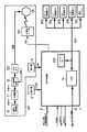
図5は、信号処理部4とブラック現像器メモリ206と、感光ドラムメモリ207の信号のやりとりに着目した図である。
【0044】
同図で、感光ドラムカートリッジ側(CRG側)のコネクタ(第1のコネクタ)196は、一方がコネクタ嵌合面とされ、他方がICソケット形状となっており、感光ドラムメモリ、即ち、EEPROM207が前記ソケットに挿入された状態で感光ドラムカートリッジ199に取り付けられる。そして、プリンタ本体に取り付けられた本体側コネクタ(第2のコネクタ)195と嵌合して、信号処理部4のCPU14に信号が送られる。
【0045】
EEPROM207に供給されるVccは、CPU14によりON/OFFできる構成となっていてCPUポートのVCCONが「LOW」で電源ON、「High」で電源OFFとなる。CPU14はEEPROMのリード動作或はライト動作のときに電源の供給をONして、リード時には、クロック信号182に同期してデータ信号184を読み込み、ライト時には、クロック信号182に同期してデータ信号183をEEPROMに送出してメモリに書き込む。信号186は感光ドラム有無検出信号であり、CPU14が監視して、「LOW」で感光ドラムカートリッジ無し、「High」で感光ドラムカートリッジ有りの判断をする。この有無検出信号は、感光ドラムカートリッジが本体に挿入されコネクタ同士が嵌合されると、EEPROMのVccがリターンされ、「High」となる。
【0046】
又、CRG側コネクタ198は、ブラック現像器メモリEEPROM206が挿入された状態でブラック色の現像カートリッジに取り付けられる。信号のやり取りについては、前述の感光ドラムカートリッジの場合と同様である。
【0047】
EEPROM207と206はいづれもDip形状のICであり、CRG側コネクタ196と198に直に接続される。図6は、Dip形状のEEPROM−ICのピン配置の一例である。
【0048】
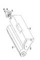
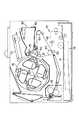
図7は、感光ドラムカートリッジ199と、前述のEEPROM207と、カートリッジ側コネクタ196との取り付け態様を示す。感光ドラムカートリッジ199は、主に感光ドラム100と、廃トナー容器180と、EEPROM207と、カートリッジ側コネクタ196と、前記コネクタ196とカートリッジとを接続するネジ360とにて構成される。
【0049】
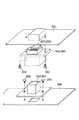
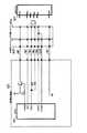
図8は、カートリッジ側コネクタ196(又は198)と本体側コネクタ195(又は197)とEEPROM207(又は206)の形状を示した図である。図のようにカートリッジ側コネクタ196は感光ドラムカートリッジ199のコネクタ取り付け部354にねじ360によって固定される。本体側コネクタ195は、本体の取り付け部358にねじ356によって固定される。
【0050】
図9は、図8に示すカートリッジ側コネクタ196(又は198)と本体側コネクタ195(又は197)の断面図である。
【0051】
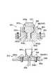
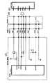
本発明のカートリッジ側コネクタ196は、その内部にコネクタのコンタクト(接触端子)352を有しIC207と接触を取る構成となっている。このカートリッジ側コネクタ196は、カートリッジに対し固定される。一方、これに相対する画像形成装置本体側コネクタ195は、画像形成装置本体の一部であるコネクタ取付部358に対して、小ねじ356で固定される。ただし、カートリッジ側に実装されたコネクタ196は、カートリッジに対して、確実に固定されているために、カートリッジと画像形成装置本体との嵌合時のずれがコネクタ196、195間にかからないようにする必要がある。画像形成装置本体側コネクタ195を可動(フローティング)なように画像形成装置本体のコネクタ取付部358に対して固定する必要がある。図9に記載した断面図は、それを考慮したものであり小ねじ356は、画像形成装置本体のコネクタ取付部358に対して固定されるものの、小ねじ356と画像形成装置本体側コネクタ195に設けられた小ねじ用穴357aには、先に説明したずれを吸収すべく余裕を有するように小ねじ356との間に隙間を生ずる大きさとしてある。従って、画像形成装置本体側コネクタ195は画像形成装置本体のコネクタ取付部358に対して移動可能な状態になるように小ねじ356を雌ねじ358aにねじ込んで取り付けられている。
【0052】
カートリッジ側コネクタ196は合成樹脂製であって、中空の方形断面の根本側外壁353aから先端が中空の嵌合部353bとなっている。カートリッジ側コネクタ196の中空部には対向する壁間を連結するIC取付部353cが一体形成されている。又は、嵌着により外壁部353a及び嵌合部353bに取り付けられている。その断面は図9に示すようにT字形をしている。そして、根本側外壁部353aと嵌合部353bの対向二辺とIC取付部353c間に図の上下で外部に通じている端子取付空間353dを設けている。IC取付部353cに沿ってコンタクト352が配され、コンタクト352の図9における下端はIC取付部353cから両側へ向って離れている。このコンタクト352は、画像形成装置本体側コンタクト355との接触を確実にするため、先端に外方へ向って変形させた接点部352aを備えている。IC207はチップ本体351aがIC取付部353cの直上で隙間を置いて配され、IC207のリード線351bは端子取付空間353dに上部から進入し、コンタクト352に圧接している。
【0053】
画像形成装置本体側コネクタ195は前述の小ねじ用穴357aを設ける取付部357bに一体に四角形箱形の嵌合部357cが設けられ、該画像形成装置本体側コネクタ195に固定されたコンタクト355に配線359が結合されている。該コンタクト355は嵌合部357cの対向内側面に接している。カートリッジを画像形成装置本体に装着する際、カートリッジ側コネクタ196の嵌合部353b内周は画像形成装置本体側コネクタ195の嵌合部357c外周に嵌合すると共に、カートリッジ側コンタクト352の接点部352aは画像形成装置側コンタクト355に圧接して先端が近寄る方向に変形して該コネクタに導通する。
【0054】
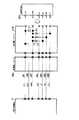
図10は、カートリッジ側コネクタ196の断面図であり、図9の断面図を90°回転したものである。同図は、EEPROM−ICの5ピンから8ピンを結ぶ面での断面図である。図のように、ICの7ピンにはコンタクト352は接続されない。そして、ICの8ピン(電源Vcc)に接するコンタクト352が途中で二股に分かれて(361の部分)嵌合部353bまでコンタクトが延びている。
【0055】
又、ICに5ピンのGND信号は、コネクタ嵌合時に他のピンに先じて接続され、コネクタを抜くときには最後に離れるように、他のピンよりも長いコンタクトにしてある。これにより、EEPROMに静電気が蓄積されている場合でもGNDピンを介して電荷が放出されるので、嵌合時に静電気でEEPROMの入力出ポートを破壊することが防げる。
【0056】
本実施例では、プロセスカートリッジである感光ドラムカートリッジ199を例にとって説明したが、マゼンタ、シアン、イエロー、ブラックトナーの入っている現像トナーカートリッジについても同様にしてEEPROMを取り付けてもよい。又、感光ドラムと、現像剤を収容した現像器と、廃トナー容器とが一体となっているプロセスカートリッジに、上述のコネクタとメモリを搭載してもよい。
【0057】
又、本実施例ではメモリICをEEPROMであるとして説明したが、他の不揮発性メモリでもよい。
【0058】
更に、本実施例では、EEPROMに供給されるVccを本体側へリターンさせたが、同じ様にEEPROMに供給されるGND信号やEEPROM制御信号を本体側へリターンさせてもよい。図11にEEPROM制御信号であるチップセレクト信号CSをリターンして感光ドラムカートリッジの有無を検出する場合の構成を示す。
【0059】
実施例2
図12に本発明の第2の実施例を示す。同図は感光ドラムカートリッジ有無検出を行うための本体側CPUとEEPROMの配線について示した図である。
【0060】
本実施例では、EEPROMの制御信号はリターンせずに、独立した2本の信号線をカートリッジ側コネクタ409に加えて、例えば、カートリッジ側コネクタ409が嵌合していない場合には、抵抗R6によってプルアップされて「High」レベルであり、カートリッジ側コネクタ409が嵌合されたときには、「LOW」レベルが有無検出信号410に表れるように構成される。
【0061】
図14に、本実施例のカートリッジ側コネクタ413の外形図を示す。図のようにICソケットの5ピン(GNDピン)から金属板414を延長して、この金属板と1ピンにはダイオードD3を、2ピンにはダイオードD2を、3ピンにはダイオードD1を、8ピンにはコンデンサC1を接続する。金属板414とD1〜D3とC1の接続には、例えば半田付けを行う。この状態で、同図の上方向からICソケットめがけて、EEPROMを挿入する。
【0062】
本実施例により、低コストのまま、より信頼性を高めることが可能となる。
【0063】
実施例3
図13に本発明の第3の実施例を示す。本図は、プリンタ本体の信号処理部4とカートリッジ上のEEPROMの配線について示した図である。本実施例では、感光ドラムカートリッジのEEPROMについてのみ説明されるが、他の各色の現像カートリッジも同様に考えてよい。
【0064】
信号処理部4と本体側コネクタ195とEEPROM207と信号181〜187については実施例1と同様である。本実施例ではカートリッジ側コネクタ413に図示するようにコンデンサC1とダイオードD1〜D3が実装してある。コンデンサC1は、EEPROMのプログラム時にEEPROMから発生するVccへのノイズを平滑する機能と、Vccラインへ外部から印加される静電気を吸収し、EEPROMに影響を及ぼさない様にする機能がある。ダイオードD1〜D3は、CSライン、SKライン、DIラインへ外部から印加される静電気をGNDラインに逃がしてEEPROMに影響を及ぼさない様にする機能がある。
【0065】
実施例4
図15に本発明の第4の実施例の電気ブロック図を示し、図16にCPU14の制御フローチャートを示す。図15において、第1実施例と同じ機能を有する部材については同じ番号が付されている。
【0066】
図15にて、感光ドラムドアセンサ416は、感光ドラムカートリッジを交換若しくは取り外す際のドアの開閉を検出するスイッチである。本センサの出力信号418がドア開をしめした場合にはCPU14は、感光ドラムカートリッジがユーザによって交換若しくは取り外されると判断して、感光ドラムメモリ207の内容を更新する。感光ドラムドアセンサ416がドア開を検出してからユーザが感光ドラムカートリッジを取り外すまで、つまり感光ドラムメモリの各I/Oがプリンタ本体から切り外されるまでは、約1秒以上ある。現像器ドア開センサ415は、各色の現像器を交換もしくは取り外す際のドアの開閉を検出するスイッチである。本センサの出力信号417がドア開を示した場合にはCPU14は各色いずれかの現像器がユーザによって交換もしくは取り外されると判断して、現像器メモリ203、204、205、206の内容を更新する。現像器ドア開センサ415がドア開を検出してから、現像器がユーザによって取り外されるまでは、約1秒以上はある。
【0067】
図16に、感光ドラムメモリを例にとったフローチャートを示す。
【0068】
先ず、プリンタ本体の電源を投入すると(419)、感光ドラムカートリッジドアが閉まっていることを確認する(420)。感光ドラムカートリッジドアが閉まっている場合には、感光ドラムメモリ207にVccを供給(421)して、感光ドラムカートリッジが有ることを確認する(422)。この確認方法は、実施例1で説明したように、カートリッジ側コネクタのVccのリターン信号の論理レベルで判断を行う。カートリッジ無しの場合には表示パネル又はホストコンピュータを介してユーザに報知して、カートリッジ有りの場合には感光ドラムメモリであるEEPROMから所望の情報をリードする(423)。この状態でプリンタはスタンバイ状態となり、印字を行える状態となる。そして、印字を行った後に、感光ドラムカートリッジドアが開いていなければ(425)、次にプリンタ本体のメインスイッチの状態を参照して(426)メインスイッチがONのままであれば、印字動作まちの状態(424)に戻る。
【0069】
一方、感光ドラムカートリッジドアが開である場合には(425)、感光ドラムメモリ207の内容を更新して(429)、VccをOFF(428)する。また、メインスイッチがOFFした場合には(426)、感光ドラムメモリ207の内容を更新して(430)、VccをOFF(431)して、プリンタ全体の電源をOFFする(432)。
【0070】
なお、感光ドラムメモリ207の更新する情報とは、例えば、感光ドラムの残寿命データや印字枚数等のデータである。
【0071】
実施例5
実施例1〜4においては、感光ドラム100に形成されたトナー像を転写ドラム103に担持された転写紙Pに転写するカラーレーザビームプリンタに本発明を適用した場合について説明したが、実施例5においては、本発明は、図17に示すように、感光ドラム71に形成されたトナー像を一旦中間転写ユニットに転写し、その後中間転写ユニットから転写紙Pにトナー像を一括転写するカラーレーザビームプリンタに適用される。
【0072】
つまり、図17において、感光ドラム71は、不図示の駆動手段によって図示矢印方向に駆動され、ローラー帯電器72により所定の電位に均一に帯電される。次いで、イエローの画像模様に従った信号が入力された露光装置73により、レーザ光が感光ドラム71に照射され、感光ドラム71上に潜像が形成される。
【0073】
更に感光ドラム71が矢印方向に進むと支持体75に支持された現像装置74a、74b、74c、74dのうち、例えばイエロートナーが収容された現像装置74aが感光ドラム71に対向するように支持体5が回転され、上記の潜像は現像装置74aによって可視化される。次いで、現像されたトナー像は中間転写体である中間転写ベルト66上に転写される。
【0074】
中間転写ベルト66は3本の支持ローラー61、62、63上に張設され、不図示の駆動源に連結された支持ローラー62が回転することにより、図中矢印方向に移動する。又、中間転写ベルト66の内側の感光ドラム対向部には、一次転写ローラ64が設けられ、不図示の高圧電源から所定のバイアスが印加され、感光ドラム71上のトナーは中間転写ベルト66上に転写される。
【0075】
以上の工程を更に例えばマゼンタ、シアン、黒の順に現像装置74b、74c、74dにより実施することによって中間転写ベルト66上に4色のトナー像が形成される。
【0076】
この4色のトナー像は、中間転写ベルト66の移動と同期をとって給紙装置76から搬送手段77を介して搬送された転写紙P上に、2次転写ローラー65により一括転写される。更に、転写紙は、加熱・加圧定着装置78によって溶融固着されカラー画像が得られる。
【0077】
感光ドラム71上の転写残トナーはブレード手段を備えたクリーニング装置79によって清掃される。
【0078】
又、本実施例においては、帯電ローラー72、感光ドラム71、及びクリーニング装置79が一体のプロセスカートリッジ90として構成され、装置本体に対して装着ガイド手段80により脱着自在とされている。更に、上記各実施例と同様に、第1及び第2のコネクタを備えたメモリICを備え、同様に機能する本発明のコネクタ84を備えている。
【0079】
尚、4色の各現像器74a〜74dもプロセスカートリッジと同様に、装置本体と脱着可能な構成とされている。これらの構成により、従来サービスマンが行なっていた上記部材の交換、メンテナンスをユーザが簡単に行なうことができる。
【0080】
上記のような構成のフルカラー画像形成装置に、実施例1、2、3及び4にて説明した本発明を適用することにより、上記と同様の作用効果を得ることができる。
【0081】
【発明の効果】
以上説明したように、本発明では、カートリッジコネクタが有するソケットがメモリ部材を直接保持し、さらに前記ソケットの内部に、カートリッジを装置本体に装着した際に、装置本体からメモリ部材に供給する電源信号を短絡するか、或いは、メモリ部材を接地するためのGND信号を短絡する短絡接触端子を設けたことによって、カートリッジ、または、プロセスカートリッジ、及び、電子写真画像形成装置を小型化することができるとともに、カートリッジ、または、プロセスカートリッジの装着の有無を判別するための部品を格別設けることなく、カートリッジ、または、プロセスカートリッジの装着の有無を判別することができる。
【図面の簡単な説明】
【図1】本発明の画像形成装置の一実施例のカラーレーザビームプリンタの概略構成側面断面図である。
【図2】図1のカラーレーザビームプリンタの機能構成を説明するブロック図である。
【図3】図1のカラーレーザビームプリンタのプリンタエンジンの機能構成を説明するブロック図である。
【図4】画像形成プロセスにおける垂直同期信号(VSYNC)、水平同期信号(HSYNC)及び画像信号(VDO)のタイミングを示す図である。
【図5】コネクタを介して行なう信号処理部と、ブラック現像器メモリ及び感光ドラムメモリとの間の信号の送受信の一実施例を説明する図である。
【図6】Dip形状のEEPROM−ICのピン配置を示す図である。
【図7】プロセスカートリッジ(感光ドラムカートリッジ)の斜視図である。
【図8】カートリッジ側コネクタと本体側コネクタとを備えた本発明のコネクタの一実施例の分解斜視図である。
【図9】図8のコネクタの断面図である。
【図10】カートリッジ側コネクタの拡大断面図である。
【図11】コネクタを介して行なう信号処理部と感光ドラムメモリとの間の信号の送受信の他の実施例を説明する図である。
【図12】コネクタを介して行なう信号処理部と感光ドラムメモリとの間の信号の送受信の他の実施例を説明する図である。
【図13】コネクタを介して行なう信号処理部と感光ドラムメモリとの間の信号の送受信の他の実施例を説明する図である。
【図14】カートリッジ側コネクタの一実施例の外形図である。
【図15】カラーレーザビームプリンタのプリンタエンジンの他の実施例の機能構成を説明するブロック図である。
【図16】CPUの制御態様の一実施例を示すフローチャートである。
【図17】本発明の画像形成装置の他の実施例のカラーレーザビームプリンタの概略構成側面断面図である。
【符号の説明】
1 画像形成装置
4 信号処理部
14 CPU
77、102 搬送手段
80 装着手段
71、100 感光ドラム
111 帯電器
112 クリーニングブレード
180 廃トナー容器
195、197、403、408 本体側コネクタ
196、198、404、409、413 カートリッジ側コネクタ
199 プロセスカートリッジ(感光ドラムカートリッジ)
203〜206 EEPROM(現像器メモリ)
206、207 EEPROM(感光ドラムメモリ)[0001]
BACKGROUND OF THE INVENTION
The present invention comprises an IC such as an EEPROM and is used to couple or separate electrical circuits.cartridgeConnector, process cartridge having the connector, andElectronic photographyImage formationEquipmentIt is related. This connector can also be suitably used for a fixing unit other than the process cartridge, an intermediate transfer unit, and the like that are detachably formed on the main body of the image forming apparatus.
[0002]
Here, examples of the image forming apparatus include an electrophotographic copying machine, an electrophotographic printer (for example, an LED printer, a laser beam printer, etc.), an electrophotographic facsimile apparatus, and an electrophotographic word processor.
[0003]
The process cartridge is a cartridge in which a charging unit, a developing unit or a cleaning unit and an electrophotographic photosensitive member are integrally formed, and the cartridge can be attached to and detached from the image forming apparatus main body. Or at least one of developing means, developing means, and cleaning means, and an electrophotographic photosensitive member are integrated into a cartridge so as to be removable from the main body of the electrophotographic image forming apparatus, or at least the developing means and the electrophotographic photosensitive member. Are integrated into a cartridge so as to be detachable from the main body of the electrophotographic image forming apparatus.
[0004]
[Prior art]
Conventionally, in an image forming apparatus using an electrophotographic image forming process, the electrophotographic photosensitive member and the process means acting on the electrophotographic photosensitive member are integrally formed into a cartridge, and the cartridge can be attached to and detached from the image forming apparatus main body. The process cartridge method is adopted. According to this process cartridge system, the maintenance of the apparatus can be performed by the user himself / herself without depending on the service person, so that the operability can be remarkably improved. Therefore, this process cartridge system is widely used in image forming apparatuses.
[0005]
In particular, in a color laser beam printer, a process cartridge (photosensitive drum cartridge) in which an electrophotographic photosensitive member, a cleaning unit, and a waste toner container are integrated, and development of each color containing magenta, cyan, yellow, and black toners. Maintenance-free is realized by making the cartridge detachable from the main body of the image forming apparatus.
[0006]
In such an image forming apparatus, for example, when the functions of the components incorporated in the process cartridge deteriorate due to long-term use, the entire process cartridge is replaced. This replacement operation is an extremely simple operation in which the image forming apparatus main body is opened with one touch, an old process cartridge is taken out from the inside of the apparatus main body, and a new process cartridge is attached to the apparatus main body. To get.
[0007]
Furthermore, recently, in order to further improve the above-described conventional technology and improve the usability of the user of the image forming apparatus, the following functions, that is,
(1) By mounting an electronic device such as a memory on a process cartridge, data such as manufacturing conditions is written at the time of manufacture and shipment. When this process cartridge is mounted on the image forming apparatus body, the image forming apparatus refers to this data, A function to perform an image forming operation under the optimum conditions of the process cartridge.
(2) A function that makes it possible to sequentially refer to the remaining life of the photosensitive drum by detecting the remaining life of the photosensitive drum during the image forming operation and holding this data in a memory.
(3) The diagnostic data of the main body of the image forming apparatus is held in the memory of the process cartridge, and the service provider can quickly respond to the service by referring to the contents when an abnormality occurs or during maintenance. Self-diagnosis function.
Attempts have been made to add.
[0008]
When the above function is added to the image forming apparatus, an electronic device such as an EEPROM needs to be mounted on a detachable unit such as a process cartridge. In a conventional process cartridge equipped with these electronic devices, an electronic device such as a memory and a connector are provided on a printed circuit board, and the printed circuit board is mounted on the process cartridge.
[0009]
In addition, when mounting electrical components on a process cartridge that can be attached to and detached from the apparatus body in this way, an IC such as a non-volatile memory on the printed circuit board, and an IC from an external surgepulseIn general, electronic parts and functional parts such as diodes, resistors, capacitors, connectors, and the like for protection from the like are mounted on a printed circuit board.
[0010]
The connector is not a board-mounted type, but is drawn out with a cable.
[0011]
[Problems to be solved by the invention]
The present invention is a further development of the conventional technology described in detail later.
[0012]
It is an object of the present invention to determine whether or not a process cartridge or the like that is inexpensive and compact with an electronic device, for example, an IC such as an EEPROM, is attached to the apparatus body. Can be realized without additional partscartridgeConnector, process cartridge having such a connector, andElectronic photographyImage formationEquipmentIs to provide.
[0013]
Another object of the present invention is to provide the above-described connector with better noise resistance, a process cartridge having such a connector, andElectronic photographyImage formationEquipmentIs to provide.
[0014]
Still another object of the present invention is to turn off the power supply to the electronic device and not to access the electronic device when a process cartridge or other unit that can be attached to and detached from the apparatus main body is removed. Can protect the content stored in the electronic device and increase its reliability.cartridgeConnector, process cartridge having such a connector, andElectronic photographyImage formationEquipmentIs to provide.
[0015]
[Means for Solving the Problems]
The above objects are achieved by the cartridge connector, the process cartridge, and the electrophotographic image forming apparatus according to the present invention. According to one aspect of the present invention, in a cartridge connector that can be fitted to a main body connector provided in the apparatus main body, which is used in a cartridge that is detachable from the electrophotographic image forming apparatus main body,
(I) a memory member having a plurality of lead terminals and storing information relating to the cartridge;
(Ii) A socket in which the memory member is mounted, wherein a memory member connecting portion electrically connected to one of the plurality of lead terminals on one end side and the cartridge on the other end side is mounted on the apparatus main body. A socket provided with a plurality of contact terminals inside the socket, and a main body connector connecting portion electrically connected to the main body connector,
Have
The plurality of contact terminals;One of themThe memory member connection part is separated in the middle and connected to the two main body connector connection parts to short-circuit the two main body connector connection parts.And a short-circuit contact terminal for short-circuiting a power signal supplied from the apparatus main body to the memory member when the cartridge is mounted on the apparatus main body.A cartridge connector featuringIs done.
[0016]
According to another aspect of the present invention, a cartridge that can be attached to and detached from the electrophotographic image forming apparatus main body.In the cartridge connector that can be fitted to the main body connector provided in the apparatus main body,
(iA memory member having a plurality of lead terminals for storing information relating to the cartridge;
(ii) When the memory member is attached to the socket, the memory member connecting portion electrically connected to one of the lead terminals on one end side, and the cartridge on the other end side when the cartridge is attached to the apparatus main body. A main body connector connecting portion electrically connected to the main body connector, and a socket provided with a plurality of contact terminals inside the socket;
Have
One of the plurality of contact terminals is connected to the two main body connector connection parts by separating the memory member connection part in the middle, and shorts the two main body connector connection parts. A short-circuit contact terminal provided, which is a short-circuit contact terminal for short-circuiting a GND signal for grounding the memory member when the cartridge is mounted on the apparatus main body.Provided byIs done.
[0017]
The present inventionAccording to another aspect ofA process cartridge that can be attached to and detached from the electrophotographic image forming apparatus main body,
(i) An electrophotographic photoreceptor;
(ii) Process means acting on the electrophotographic photoreceptor;
(iiiA memory member for storing information relating to the process cartridge, the cartridge connector being fitted to a main body connector provided in the apparatus main body when the process cartridge is mounted on the apparatus main body, and having a plurality of lead terminals. And a socket having the memory member attached thereto, and a contact terminal having a body connector connection portion electrically connected to the body connector when the plurality of process cartridges are attached to the apparatus body on one end side. A plurality of sockets provided inside the socket, wherein one of the plurality of contact terminals is connected to the two main body connector connection parts by separating the memory member connection part in the middle, A short-circuit contact terminal provided inside the socket for short-circuiting the two main body connector connection portions, When mounted on the apparatus main body, a cartridge connector is short-circuited contact terminals for short-circuiting the power signal supplied to the memory element from the apparatus main body,
Process cartridge characterized by havingProvided byIs done.
[0018]
According to another aspect of the present invention, a process cartridge that can be attached to and detached from an electrophotographic image forming apparatus main body,
(i) An electrophotographic photoreceptor;
(ii) Process means acting on the electrophotographic photoreceptor;
(iiiA memory member for storing information relating to the process cartridge, the cartridge connector being fitted to a main body connector provided in the apparatus main body when the process cartridge is mounted on the apparatus main body, and having a plurality of lead terminals. And a socket having the memory member attached thereto, and a contact terminal having a body connector connection portion electrically connected to the body connector when the plurality of process cartridges are attached to the apparatus body on one end side. A plurality of sockets provided inside the socket, wherein one of the plurality of contact terminals is connected to the two main body connector connection parts by separating the memory member connection part in the middle, A short-circuit contact terminal provided inside the socket for short-circuiting the two main body connector connection portions, When mounted on the apparatus main body, a cartridge connector is short-circuited contact terminals for short-circuiting the GND signal for grounding the memory member,
A process cartridge is provided.
[0019]
According to another aspect of the present invention, in an electrophotographic image forming apparatus for detaching a process cartridge and forming an image on a recording medium,
(i) Body connector,
(ii) An electrophotographic photosensitive member; process means acting on the electrophotographic photosensitive member; and a cartridge connector that fits into the main body connector when the process cartridge is mounted on a main body of the electrophotographic image forming apparatus. A memory member having a plurality of lead terminals for storing information relating to the process cartridge, and a socket in which the memory member is attached, wherein the main body when the plurality of process cartridges are attached to the apparatus main body on one end side A socket provided with a plurality of contact terminals in the socket, the main body connector connection portion electrically connected to the connector, wherein one of the plurality of contact terminals is the memory member connection portion In the middle, connect with the two main body connector connection parts and short-circuit the two main body connector connection parts. A cartridge connector which is a short-circuit contact terminal provided in the socket, and which is a short-circuit contact terminal for short-circuiting a power signal supplied from the device main body to the memory member when the cartridge is mounted on the device main body; Mounting means for detachably mounting a process cartridge having
(iii) Conveying means for conveying the recording medium;
An electrophotographic image forming apparatus is provided.
[0020]
According to another aspect of the present invention, in an electrophotographic image forming apparatus for detaching a process cartridge and forming an image on a recording medium,
(i) Body connector,
(ii) An electrophotographic photosensitive member; process means acting on the electrophotographic photosensitive member; and a cartridge connector that fits into the main body connector when the process cartridge is mounted on a main body of the electrophotographic image forming apparatus. A memory member having a plurality of lead terminals for storing information relating to the process cartridge, and a socket in which the memory member is attached, wherein the main body when the plurality of process cartridges are attached to the apparatus main body on one end side A socket provided with a plurality of contact terminals in the socket, the main body connector connection portion electrically connected to the connector, wherein one of the plurality of contact terminals is the memory member connection portion In the middle, connect with the two main body connector connection parts and short-circuit the two main body connector connection parts. A short-circuit contact terminal provided in a socket, and a cartridge connector that is a short-circuit contact terminal for short-circuiting a GND signal for grounding the memory member when the cartridge is mounted on the apparatus main body. Mounting means for detachably mounting the process cartridge;
(iii) Conveying means for conveying the recording medium;
An electrophotographic image forming apparatus is provided.
[0021]
DETAILED DESCRIPTION OF THE INVENTION
The present invention will be described below with reference to the accompanying drawings.cartridgeConnector, process cartridge having such a connector, andElectronic photographyImage formationEquipmentA preferred embodiment will be described in detail.
[0022]
Example 1
FIG. 1 shows a typical example of an image forming apparatus according to the present invention, which has a resolution of 600 dots / inch (dpi), and records an image based on multi-value data in which each pixel of each color component is expressed by 8 bits. 1 is a side sectional view showing a schematic configuration of a color laser beam printer (hereinafter simply referred to as “printer”) 1 that performs the above. In some embodiments described below, the apparatus shown in FIG. 1 is used as a common embodiment.
[0023]
In the image forming apparatus illustrated in FIG. 1, the transfer paper P fed from the
[0024]
Here, the developing devices Dy, Dc, Db, and Dm of the respective colors have rotation support shafts at both ends, and each is held by the developing device
[0025]
Next, the color image forming operation of the color laser beam printer configured as described above will be specifically described.
[0026]
First, the
[0027]
Next, a second latent image of C (cyan) color is formed on the
[0028]
Similarly, third and fourth latent images of Y (yellow) color and Bk (black) color are sequentially formed on the
[0029]
The reason why the transfer bias voltage is increased every time the toner image of each color is transferred is to prevent a decrease in transfer efficiency. The main cause of this decrease in transfer efficiency is that when the transfer paper is separated from the
[0030]
During the transfer of the fourth color, when the leading edge of the transfer paper reaches the transfer start position (including immediately before and after), an effective AC voltage of 5.5 kV (frequency is 500H).Z And a DC bias voltage +3.0 kV having the same polarity and the same potential as the transfer bias applied at the time of transferring the fourth toner image is applied to the charger 111. Thus, when transferring the fourth color, the charger 111 is operated when the leading edge of the transfer paper reaches the transfer start position in order to prevent uneven transfer. In particular, in the transfer of a full color image, even if slight transfer unevenness occurs, it is easy to notice the difference in color. Therefore, as described above, it is necessary to apply a required bias voltage to the charger 111 to perform a discharge operation. Become.
[0031]
Thereafter, when the leading edge of the transfer paper P onto which the four color toner images are superimposed and transferred approaches the separation position, the
[0032]
Next, an image forming operation by laser beam scanning will be described.
[0033]
In FIG. 1,
[0034]
The color laser beam printer of the present embodiment outputs an image with a resolution of 600 dots / inch (dpi) through the image forming process as described above.
[0035]
As input data of this apparatus, color image data (for example, data expressed by RGB components) generated by a host computer (hereinafter referred to as “host”), and other image data generation apparatuses (still image recorder, etc.) For example, image data generated in the above and stored in some storage medium can be considered. For this reason, as shown in FIG. 1, this apparatus is provided with a
[0036]
In some embodiments described below, color image data sent from a host is considered as input data.
[0037]
FIG. 2 is a block diagram illustrating a functional configuration of the
[0038]
Various image signals other than the
[0039]
FIG. 3 is a block diagram showing a functional configuration of the
[0040]
On the other hand, the transfer drum 103 is rotated at a constant speed by a drive motor (not shown), the leading end of the recording paper P on the transfer drum 103 is detected by the
[0041]
The
[0042]
FIG. 4 shows the timing of the vertical synchronizing signal (VSYNC), horizontal synchronizing signal (HSYNC), and image signal (VDO) described above in the image forming process.
[0043]
FIG. 5 is a diagram focusing on the exchange of signals between the
[0044]
In the figure, one of the connectors (first connector) 196 on the photosensitive drum cartridge side (CRG side) has a connector fitting surface and the other has an IC socket shape, and the photosensitive drum memory, that is, the
[0045]
The Vcc supplied to the
[0046]
The
[0047]
The
[0048]
FIG. 7 shows how the
[0049]
FIG. 8 is a diagram showing the shapes of the cartridge side connector 196 (or 198), the main body side connector 195 (or 197), and the EEPROM 207 (or 206). As shown in the figure, the
[0050]
9 is a cross-sectional view of the cartridge side connector 196 (or 198) and the main body side connector 195 (or 197) shown in FIG.
[0051]
The cartridge-
[0052]
The cartridge-
[0053]
The image forming apparatus main
[0054]
FIG. 10 is a cross-sectional view of the cartridge-
[0055]
In addition, the 5-pin GND signal is connected to the IC prior to the other pins when the connector is fitted, and the contact is longer than the other pins so that it is finally removed when the connector is removed. As a result, even when static electricity is accumulated in the EEPROM, charges are discharged through the GND pin, so that it is possible to prevent the input / output port of the EEPROM from being destroyed by static electricity during fitting.
[0056]
In this embodiment, the
[0057]
In the present embodiment, the memory IC is described as being an EEPROM, but other nonvolatile memories may be used.
[0058]
Further, in this embodiment, Vcc supplied to the EEPROM is returned to the main body side. However, a GND signal and an EEPROM control signal supplied to the EEPROM may be similarly returned to the main body side. FIG. 11 shows a configuration for detecting the presence or absence of a photosensitive drum cartridge by returning a chip select signal CS which is an EEPROM control signal.
[0059]
Example 2
FIG. 12 shows a second embodiment of the present invention. This figure shows the wiring between the main body side CPU and the EEPROM for detecting the presence or absence of the photosensitive drum cartridge.
[0060]
In this embodiment, the EEPROM control signal does not return, and two independent signal lines are added to the
[0061]
FIG. 14 shows an external view of the
[0062]
According to the present embodiment, it is possible to further improve the reliability while keeping the cost low.
[0063]
Example 3
FIG. 13 shows a third embodiment of the present invention. This figure is a diagram showing the wiring of the
[0064]
The
[0065]
Example 4
FIG. 15 shows an electric block diagram of the fourth embodiment of the present invention, and FIG. 16 shows a control flowchart of the
[0066]
In FIG. 15, a photosensitive
[0067]
FIG. 16 shows a flowchart of the photosensitive drum memory as an example.
[0068]
First, when the printer main body is turned on (419), it is confirmed that the photosensitive drum cartridge door is closed (420). If the photosensitive drum cartridge door is closed, Vcc is supplied to the photosensitive drum memory 207 (421), and it is confirmed that there is a photosensitive drum cartridge (422). In this confirmation method, as described in the first embodiment, the determination is made based on the logical level of the Vcc return signal of the cartridge side connector. When there is no cartridge, the user is notified through the display panel or the host computer, and when there is a cartridge, desired information is read from the EEPROM which is a photosensitive drum memory (423). In this state, the printer enters a standby state and is ready for printing. After printing, if the photosensitive drum cartridge door is not open (425), referring to the state of the main switch of the printer main body (426), if the main switch remains ON, the printing operation Return to state (424).
[0069]
On the other hand, when the photosensitive drum cartridge door is open (425), the contents of the
[0070]
The information to be updated in the
[0071]
Example 5
In the first to fourth embodiments, the case where the present invention is applied to the color laser beam printer that transfers the toner image formed on the
[0072]
That is, in FIG. 17, the
[0073]
Further, when the
[0074]
The intermediate transfer belt 66 is stretched on three
[0075]
The above process is further performed by developing
[0076]
The four color toner images are collectively transferred by the secondary transfer roller 65 onto the transfer paper P conveyed from the
[0077]
Transfer residual toner on the
[0078]
In this embodiment, the charging
[0079]
Each of the four color developing devices 74a to 74d is configured to be detachable from the apparatus main body in the same manner as the process cartridge. With these configurations, the user can easily perform replacement and maintenance of the above-described members, which have been conventionally performed by service personnel.
[0080]
By applying the present invention described in the first, second, third, and fourth embodiments to the full-color image forming apparatus having the above-described configuration, the same operational effects as described above can be obtained.
[0081]
【The invention's effect】
As described above, in the present invention, the socket of the cartridge connector directly holds the memory member, and further inside the socket,When the cartridge is mounted on the apparatus main body, the power signal supplied from the apparatus main body to the memory member is short-circuited, or the GND signal for grounding the memory member is short-circuited.By providing the short-circuit contact terminal, the cartridge, the process cartridge, and the electrophotographic image forming apparatus can be reduced in size, and the parts for determining whether the cartridge or the process cartridge is mounted are special. Without being provided, it is possible to determine whether or not a cartridge or process cartridge is mounted.
[Brief description of the drawings]
FIG. 1 is a side sectional view of a schematic configuration of a color laser beam printer according to an embodiment of an image forming apparatus of the present invention.
2 is a block diagram illustrating a functional configuration of the color laser beam printer of FIG. 1. FIG.
3 is a block diagram illustrating a functional configuration of a printer engine of the color laser beam printer of FIG. 1. FIG.
FIG. 4 is a diagram illustrating timings of a vertical synchronization signal (VSYNC), a horizontal synchronization signal (HSYNC), and an image signal (VDO) in an image forming process.
FIG. 5 is a diagram illustrating an example of signal transmission / reception between a signal processing unit, a black developing device memory, and a photosensitive drum memory performed via a connector.
FIG. 6 is a diagram showing a pin arrangement of a Dip-shaped EEPROM-IC.
FIG. 7 is a perspective view of a process cartridge (photosensitive drum cartridge).
FIG. 8 is an exploded perspective view of an embodiment of the connector of the present invention including a cartridge side connector and a main body side connector.
9 is a cross-sectional view of the connector of FIG.
FIG. 10 is an enlarged cross-sectional view of a cartridge side connector.
FIG. 11 is a diagram for explaining another embodiment of signal transmission / reception between the signal processing unit and the photosensitive drum memory via the connector.
FIG. 12 is a diagram for explaining another embodiment of signal transmission / reception between the signal processing unit and the photosensitive drum memory performed via the connector.
FIG. 13 is a diagram for explaining another embodiment of signal transmission / reception between a signal processing unit and a photosensitive drum memory via a connector.
FIG. 14 is an external view of an embodiment of the cartridge side connector.
FIG. 15 is a block diagram illustrating a functional configuration of another embodiment of a printer engine of a color laser beam printer.
FIG. 16 is a flowchart illustrating an example of a control mode of a CPU.
FIG. 17 is a side sectional view of a schematic configuration of a color laser beam printer according to another embodiment of the image forming apparatus of the present invention.
[Explanation of symbols]
1 Image forming device
4 Signal processor
14 CPU
77, 102 Conveying means
80 Wearing means
71, 100 Photosensitive drum
111 charger
112 Cleaning blade
180 Waste toner container
195, 197, 403, 408 Body side connector
196, 198, 404, 409, 413 Cartridge side connector
199 Process cartridge (photosensitive drum cartridge)
203-206 EEPROM (developer memory)
206, 207 EEPROM (photosensitive drum memory)
Claims (6)
Translated fromJapanese(i)複数のリード端子を有する、前記カートリッジに関する情報を記憶するメモリ部材と、
(ii)前記メモリ部材を装着したソケットであって、一端側に前記複数のリード端子うちの一つと電気的に接続したメモリ部材接続部と、他端側に前記カートリッジを前記装置本体に装着した際に前記本体コネクタと電気的に接続する本体コネクタ接続部と、を有する接触端子を前記ソケットの内部に複数設けたソケットと、
を有し、
前記複数の接触端子のうち一つは、前記メモリ部材接続部が途中で別れて二つの前記本体コネクタ接続部と接続して、前記二つの前記本体コネクタ接続部を短絡する、前記ソケットの内部に設けられた短絡接触端子であって、前記カートリッジを前記装置本体に装着した際に、前記装置本体から前記メモリ部材に供給する電源信号を短絡する短絡接触端子であることを特徴とするカートリッジコネクタ。In a cartridge connector that can be fitted to a main body connector provided in the apparatus main body, which is used for a cartridge that can be attached to and detached from the electrophotographic image forming apparatus main body,
(I) a memory member having a plurality of lead terminals and storing information relating to the cartridge;
(Ii) A socket in which the memory member is mounted, wherein a memory member connecting portion electrically connected to one of the plurality of lead terminals on one end side and the cartridge on the other end side is mounted on the apparatus main body. A socket provided with a plurality of contact terminals inside the socket, and a main body connector connecting portion electrically connected to the main body connector,
Have
One of the plurality of contact terminalsis connected to the two main body connector connection parts by separating the memory member connection part in the middle, and short-circuits the two main body connector connection parts. A cartridge connector, wherein the cartridge connectoris a short-circuit contact terminal that short-circuits a power signal supplied from the device main body to the memory member when the cartridge is mounted on the device main body .
(i)複数のリード端子を有する、前記カートリッジに関する情報を記憶するメモリ部材と、
(ii)前記メモリ部材を装着したソケットであって、一端側に前記複数のリード端子うちの一つと電気的に接続したメモリ部材接続部と、他端側に前記カートリッジを前記装置本体に装着した際に前記本体コネクタと電気的に接続する本体コネクタ接続部と、を有する接触端子を前記ソケットの内部に複数設けたソケットと、
を有し、
前記複数の接触端子のうち一つは、前記メモリ部材接続部が途中で別れて二つの前記本体コネクタ接続部と接続して、前記二つの前記本体コネクタ接続部を短絡する、前記ソケットの内部に設けられた短絡接触端子であって、前記カートリッジを前記装置本体に装着した際に、前記メモリ部材を接地するためのGND信号を短絡する短絡接触端子であることを特徴とするカートリッジコネクタ。In a cartridge connector that can be fitted to a main body connector provided in the apparatus main body, which is used for a cartridge that can be attached to and detached from the electrophotographic image forming apparatus main body,
(I) a memory member having a plurality of lead terminals and storing information relating to the cartridge;
(Ii) A socket in which the memory member is mounted, wherein a memory member connecting portion electrically connected to one of the plurality of lead terminals on one end side and the cartridge on the other end side is mounted on the apparatus main body. A socket provided with a plurality of contact terminals inside the socket, and a main body connector connecting portion electrically connected to the main body connector,
Have
One of the plurality of contact terminalsis connected to the two main body connector connection parts by separating the memory member connection part in the middle, and short-circuits the two main body connector connection parts. A cartridge connector, wherein the cartridge connectoris a short-circuit contact terminal that short-circuits a GND signal for grounding the memory member when the cartridge is mounted on the apparatus main body .
(i)電子写真感光体と、
(ii)前記電子写真感光体に作用するプロセス手段と、
(iii)前記プロセスカートリッジを前記装置本体に装着した際に、前記装置本体に設けられた本体コネクタと嵌合するカートリッジコネクタであって、複数のリード端子を有する、前記プロセスカートリッジに関する情報を記憶するメモリ部材と、前記メモリ部材を装着したソケットであって、一端側に前記複数のプロセスカートリッジを前記装置本体に装着した際に前記本体コネクタと電気的に接続する本体コネクタ接続部と、を有する接触端子を前記ソケットの内部に複数設けたソケットと、を有し、前記複数の接触端子のうち一つは、前記メモリ部材接続部が途中で別れて二つの前記本体コネクタ接続部と接続して、前記二つの前記本体コネクタ接続部を短絡する、前記ソケットの内部に設けられた短絡接触端子であって、前記カートリッジを前記装置本体に装着した際に、前記装置本体から前記メモリ部材に供給する電源信号を短絡する短絡接触端子であるカートリッジコネクタと、
を有することを特徴とするプロセスカートリッジ。A process cartridge that can be attached to and detached from the electrophotographic image forming apparatus main body,
(I) an electrophotographic photoreceptor;
(Ii) process means acting on the electrophotographic photoreceptor;
(Iii) A cartridge connector that fits with a main body connector provided in the apparatus main body when the process cartridge is attached to the apparatus main body, and stores information related to the process cartridge having a plurality of lead terminals. A contact having a memory member and a socket in which the memory member is mounted, and having a main body connector connecting portion electrically connected to the main body connector when the plurality of process cartridges are mounted in the apparatus main body on one end side A socket provided with a plurality of terminals inside the socket, andone of the plurality of contact terminals is connected to the two main body connector connection parts by separating the memory member connection part in the middle, shorting the two said main connector part, saida short circuit contact terminals provided in the interior of thesocket, the cart The Tsu di when mounted on the apparatus main body, a cartridge connectoris short-circuited contact terminals for short-circuiting the power signal supplied to the memory element from the apparatus main body,
A process cartridge comprising:
(i)電子写真感光体と、
(ii)前記電子写真感光体に作用するプロセス手段と、
(iii)前記プロセスカートリッジを前記装置本体に装着した際に、前記装置本体に設けられた本体コネクタと嵌合するカートリッジコネクタであって、複数のリード端子を有する、前記プロセスカートリッジに関する情報を記憶するメモリ部材と、前記メモリ部材を装着したソケットであって、一端側に前記複数のプロセスカートリッジを前記装置本体に装着した際に前記本体コネクタと電気的に接続する本体コネクタ接続部と、を有する接触端子を前記ソケットの内部に複数設けたソケットと、を有し、前記複数の接触端子のうち一つは、前記メモリ部材接続部が途中で別れて二つの前記本体コネクタ接続部と接続して、前記二つの前記本体コネクタ接続部を短絡する、前記ソケットの内部に設けられた短絡接触端子であって、前記カートリッジを前記装置本体に装着した際に、前記メモリ部材を接地するためのGND信号を短絡する短絡接触端子であるカートリッジコネクタと、
を有することを特徴とするプロセスカートリッジ。A process cartridge that can be attached to and detached from the electrophotographic image forming apparatus main body,
(I) an electrophotographic photoreceptor;
(Ii) process means acting on the electrophotographic photoreceptor;
(Iii) A cartridge connector that fits with a main body connector provided in the apparatus main body when the process cartridge is attached to the apparatus main body, and stores information related to the process cartridge having a plurality of lead terminals. A contact having a memory member and a socket in which the memory member is mounted, and having a main body connector connecting portion electrically connected to the main body connector when the plurality of process cartridges are mounted in the apparatus main body on one end side A socket provided with a plurality of terminals inside the socket, andone of the plurality of contact terminals is connected to the two main body connector connection parts by separating the memory member connection part in the middle, shorting the two said main connector part, saida short circuit contact terminals provided in the interior of thesocket, the cart The Tsu di when mounted on the apparatus main body, a cartridge connectoris short-circuited contact terminals for short-circuiting the GND signal for grounding the memory member,
A process cartridge comprising:
(i)本体コネクタと、
(ii)電子写真感光体と、前記電子写真感光体に作用するプロセス手段と、前記プロセスカートリッジを前記電子写真画像形成装置の装置本体に装着した際に、前記本体コネクタと嵌合するカートリッジコネクタであって、複数のリード端子を有する、前記プロセスカートリッジに関する情報を記憶するメモリ部材と、前記メモリ部材を装着したソケットであって、一端側に前記複数のプロセスカートリッジを前記装置本体に装着した際に前記本体コネクタと電気的に接続する本体コネクタ接続部と、を有する接触端子を前記ソケットの内部に複数設けたソケットと、を有し、前記複数の接触端子のうち一つは、前記メモリ部材接続部が途中で別れて二つの前記本体コネクタ接続部と接続して、前記二つの前記本体コネクタ接続部を短絡する、前記ソケットの内部に設けられた短絡接触端子であって、前記カートリッジを前記装置本体に装着した際に、前記装置本体から前記メモリ部材に供給する電源信号を短絡する短絡接触端子であるカートリッジコネクタと、を有するプロセスカートリッジを取り外し可能に装着する装着手段と、
(iii)前記記録媒体を搬送する搬送手段と、
を有することを特徴とする電子写真画像形成装置。In an electrophotographic image forming apparatus for detaching a process cartridge and forming an image on a recording medium,
(I) the body connector;
(Ii) an electrophotographic photosensitive member, process means acting on the electrophotographic photosensitive member, and a cartridge connector that fits into the main body connector when the process cartridge is attached to the main body of the electrophotographic image forming apparatus. A memory member having a plurality of lead terminals for storing information on the process cartridge, and a socket in which the memory member is attached, wherein the plurality of process cartridges are attached to the apparatus main body on one end side. anda socket provided with a plurality of contact terminals inside the socket having a body connector connecting portion for connecting the main body connector electrically,one of the plurality of contact terminals, the memory member connected The part is separated in the middle and connected to the two main body connector connection parts, and the two main body connector connection parts are short-circuited. Whereina short-circuit contact terminals provided in the interior of thesocket, upon mounting the cartridge to the apparatus main body, a cartridge connector anda shorting contact terminals for short-circuiting the power signal supplied to the memory member from the main assembly of the apparatus Mounting means for detachably mounting a process cartridge having
(Iii) conveying means for conveying the recording medium;
An electrophotographic image forming apparatus comprising:
(i)本体コネクタと、
(ii)電子写真感光体と、前記電子写真感光体に作用するプロセス手段と、前記プロセスカートリッジを前記電子写真画像形成装置の装置本体に装着した際に、前記本体コネクタと嵌合するカートリッジコネクタであって、複数のリード端子を有する、前記プロセスカートリッジに関する情報を記憶するメモリ部材と、前記メモリ部材を装着したソケットであって、一端側に前記複数のプロセスカートリッジを前記装置本体に装着した際に前記本体コネクタと電気的に接続する本体コネクタ接続部と、を有する接触端子を前記ソケットの内部に複数設けたソケットと、を有し、前記複数の接触端子のうち一つは、前記メモリ部材接続部が途中で別れて二つの前記本体コネクタ接続部と接続して、前記二つの前記本体コネクタ接続部を短絡する、前記ソケットの内部に設けられた短絡接触端子であって、前記カートリッジを前記装置本体に装着した際に、前記メモリ部材を接地するためのGND信号を短絡する短絡接触端子であるカートリッジコネクタと、を有するプロセスカートリッジを取り外し可能に装着する装着手段と、
(iii)前記記録媒体を搬送する搬送手段と、
を有することを特徴とする電子写真画像形成装置。In an electrophotographic image forming apparatus for detaching a process cartridge and forming an image on a recording medium,
(I) the body connector;
(Ii) an electrophotographic photosensitive member, process means acting on the electrophotographic photosensitive member, and a cartridge connector that fits into the main body connector when the process cartridge is attached to the main body of the electrophotographic image forming apparatus. A memory member having a plurality of lead terminals for storing information on the process cartridge, and a socket in which the memory member is attached, wherein the plurality of process cartridges are attached to the apparatus main body on one end side. anda socket provided with a plurality of contact terminals inside the socket having a body connector connecting portion for connecting the main body connector electrically,one of the plurality of contact terminals, the memory member connected The part is separated in the middle and connected to the two main body connector connection parts, and the two main body connector connection parts are short-circuited. Whereina short-circuit contact terminals provided in the interior of thesocket, upon mounting the cartridge to the apparatus main body, and a cartridge connectoris short-circuited contact terminals for short-circuiting the GND signal for grounding the memory member A mounting means for detachably mounting the process cartridge having,
(Iii) conveying means for conveying the recording medium;
An electrophotographic image forming apparatus comprising:
Priority Applications (8)
| Application Number | Priority Date | Filing Date | Title |
|---|---|---|---|
| JP21422496AJP3715723B2 (en) | 1996-07-24 | 1996-07-24 | Cartridge connector, process cartridge, and electrophotographic image forming apparatus |
| US08/898,575US5907748A (en) | 1996-07-24 | 1997-07-22 | Electrical connector, process cartridge and electrophotographic image forming apparatus |
| TW086110406ATW358171B (en) | 1996-07-24 | 1997-07-22 | Electrical connector, process cartridge and electrophotographic image forming apparatus |
| EP97305504AEP0821445B1 (en) | 1996-07-24 | 1997-07-23 | Electrical connector, process cartridge and electrophotographic image forming apparatus |
| DE69710394TDE69710394T2 (en) | 1996-07-24 | 1997-07-23 | Electrical connector, toner cartridge and printer |
| CN97115448ACN1074178C (en) | 1996-07-24 | 1997-07-24 | Electrical connector, process cartridge and electrophotographic image forming apparatus |
| KR1019970034641AKR100265021B1 (en) | 1996-07-24 | 1997-07-24 | Electrical connector, process cartridge and electrophotographic image forming apparatus |
| HK98105240.0AHK1005968B (en) | 1996-07-24 | 1998-06-12 | Electrical connector, process cartridge and electrophotographic image forming apparatus |
Applications Claiming Priority (1)
| Application Number | Priority Date | Filing Date | Title |
|---|---|---|---|
| JP21422496AJP3715723B2 (en) | 1996-07-24 | 1996-07-24 | Cartridge connector, process cartridge, and electrophotographic image forming apparatus |
Publications (2)
| Publication Number | Publication Date |
|---|---|
| JPH1039722A JPH1039722A (en) | 1998-02-13 |
| JP3715723B2true JP3715723B2 (en) | 2005-11-16 |
Family
ID=16652263
Family Applications (1)
| Application Number | Title | Priority Date | Filing Date |
|---|---|---|---|
| JP21422496AExpired - Fee RelatedJP3715723B2 (en) | 1996-07-24 | 1996-07-24 | Cartridge connector, process cartridge, and electrophotographic image forming apparatus |
Country Status (7)
| Country | Link |
|---|---|
| US (1) | US5907748A (en) |
| EP (1) | EP0821445B1 (en) |
| JP (1) | JP3715723B2 (en) |
| KR (1) | KR100265021B1 (en) |
| CN (1) | CN1074178C (en) |
| DE (1) | DE69710394T2 (en) |
| TW (1) | TW358171B (en) |
Families Citing this family (29)
| Publication number | Priority date | Publication date | Assignee | Title |
|---|---|---|---|---|
| JPH11110093A (en)* | 1997-10-02 | 1999-04-23 | Omron Corp | Information processor |
| JPH11242371A (en)* | 1997-10-31 | 1999-09-07 | Canon Inc | Connector, unit, process cartridge and electrophotographic image forming apparatus |
| DE19812106C2 (en)* | 1998-03-19 | 2003-08-28 | Oce Printing Systems Gmbh | Printer or copier with a sub-assembly that has an electromechanical identification arrangement |
| US6144812A (en)* | 1998-03-20 | 2000-11-07 | Canon Kabushiki Kaisha | Image formation system having a memory device located in an electrophotographic process cartridge for storing data relating to image formation |
| EP2179848A1 (en) | 1998-05-18 | 2010-04-28 | Seiko Epson Corporation | Ink-jet printing apparatus and ink cartridge therefor |
| US6724895B1 (en) | 1998-06-18 | 2004-04-20 | Supersensor (Proprietary) Limited | Electronic identification system and method with source authenticity verification |
| US7137000B2 (en) | 2001-08-24 | 2006-11-14 | Zih Corp. | Method and apparatus for article authentication |
| US6922534B2 (en) | 2001-12-28 | 2005-07-26 | Canon Kabushiki Kaisha | Process cartridge and electrophotographic image forming apparatus having electrical connection for memory |
| EP1326144B1 (en)* | 2001-12-28 | 2008-09-03 | Canon Kabushiki Kaisha | Process cartridge and electrophotographic image forming apparatus |
| EP1701224A1 (en)* | 2002-02-19 | 2006-09-13 | Seiko Epson Corporation | Connector, development cartridge, and image forming apparatus |
| JP4194298B2 (en)* | 2002-05-17 | 2008-12-10 | キヤノン株式会社 | Information storage medium, unit, process cartridge, developing cartridge, and electrophotographic image forming apparatus |
| US6973276B2 (en)* | 2002-07-12 | 2005-12-06 | Matsushita Electric Industrial Co., Ltd. | Image forming apparatus |
| JP2004333730A (en)* | 2003-05-06 | 2004-11-25 | Konica Minolta Business Technologies Inc | Image forming apparatus and image forming method |
| US20110110681A1 (en)* | 2003-12-19 | 2011-05-12 | Steven Miller | Method of Making an Electronic Circuit for an Imaging Machine |
| US9296214B2 (en) | 2004-07-02 | 2016-03-29 | Zih Corp. | Thermal print head usage monitor and method for using the monitor |
| JP4794892B2 (en)* | 2005-04-11 | 2011-10-19 | キヤノン株式会社 | Process cartridge and electrophotographic image forming apparatus |
| US8721203B2 (en)* | 2005-10-06 | 2014-05-13 | Zih Corp. | Memory system and method for consumables of a printer |
| JP4929671B2 (en)* | 2005-10-19 | 2012-05-09 | 富士ゼロックス株式会社 | Image forming apparatus and control method thereof |
| JP4712526B2 (en)* | 2005-10-31 | 2011-06-29 | 京セラミタ株式会社 | Image forming apparatus |
| US20080102674A1 (en)* | 2006-10-30 | 2008-05-01 | Lexmark International, Inc. | Electrical Connectors for Toner Cartridges In An Image Forming Device |
| US7742717B2 (en)* | 2007-09-11 | 2010-06-22 | Samsung Electronics Co., Ltd. | Developing device, memory unit thereof, and image forming apparatus |
| US8200126B2 (en) | 2007-11-30 | 2012-06-12 | Lexmark International, Inc. | Toner cartridges for an image forming device |
| JP2011069933A (en)* | 2009-09-25 | 2011-04-07 | Fuji Xerox Co Ltd | Image forming apparatus and process cartridge |
| JP5659702B2 (en)* | 2010-11-02 | 2015-01-28 | 富士ゼロックス株式会社 | Image forming apparatus |
| JP4921609B2 (en)* | 2011-09-16 | 2012-04-25 | キヤノン株式会社 | Cartridge and image forming apparatus |
| US9046868B2 (en)* | 2013-05-22 | 2015-06-02 | Lexmark International, Inc. | Interlock/connector system for a replaceable item for an image forming device |
| KR200482887Y1 (en)* | 2015-12-18 | 2017-03-15 | 주식회사 지알에스코리아 | Tonner-chip housing for razer print and copy machine |
| JP2020052333A (en)* | 2018-09-28 | 2020-04-02 | ブラザー工業株式会社 | Image forming apparatus |
| TWI688841B (en)* | 2018-11-30 | 2020-03-21 | 虹光精密工業股份有限公司 | Shift circuit operating by using a capacitor, a printing head and printing device thereof |
Family Cites Families (18)
| Publication number | Priority date | Publication date | Assignee | Title |
|---|---|---|---|---|
| US3408612A (en)* | 1966-09-26 | 1968-10-29 | Sperry Rand Corp | Connector design |
| US4084869A (en)* | 1976-11-10 | 1978-04-18 | Intel Corporation | Interconnector for integrated circuit package |
| US4510553A (en)* | 1983-01-24 | 1985-04-09 | Burroughs Corporation | Electromechanical assembly for aligning, discharging, and sequentially engaging conductors of a P.C. board with a backplane |
| US4702706A (en)* | 1983-08-16 | 1987-10-27 | Thomas & Betts Corporation | Electrical connecting device including socket therefor |
| US4746310A (en)* | 1986-11-03 | 1988-05-24 | Amphenol Corporation | Electrical connector having transient suppression and front removable terminals |
| GB8711796D0 (en)* | 1987-05-19 | 1987-06-24 | Cambridge Computer Ltd | Microcomputers |
| JPH01289078A (en)* | 1988-05-16 | 1989-11-21 | Toshiba Corp | Connection confirmation method for operating status setting terminals |
| US5028809A (en)* | 1989-03-07 | 1991-07-02 | Hewlett-Packard Company | Computer bus structure permitting replacement of modules during operation |
| US4961088A (en)* | 1989-04-20 | 1990-10-02 | Xerox Corporation | Monitor/warranty system for electrostatographic reproducing machines using replaceable cartridges |
| ATE227649T1 (en)* | 1989-08-05 | 2002-11-15 | Canon Kk | INK CARTRIDGE |
| DE4114921A1 (en)* | 1991-05-07 | 1992-11-12 | Ahlborn Mess Und Regelungstech | Electrical plug connector with multiple pins - has EEPROM memory that can be programmed with data defining specific configuration being used |
| US5208529A (en)* | 1991-07-03 | 1993-05-04 | Sym-Tek Systems, Inc. | Electric device contact assembly |
| JPH0635264A (en)* | 1992-07-14 | 1994-02-10 | Minolta Camera Co Ltd | Image forming method and its device |
| JPH0675442A (en)* | 1992-08-27 | 1994-03-18 | Minolta Camera Co Ltd | Image forming device |
| US5272503A (en)* | 1992-09-02 | 1993-12-21 | Xerox Corporation | Replaceable sub-assemblies for electrostatographic reproducing machines |
| JPH07130438A (en)* | 1993-11-02 | 1995-05-19 | Fujitsu Ltd | IC socket |
| KR0131958B1 (en)* | 1994-11-10 | 1998-10-01 | 김광호 | Process Cartridge Replacement Method and Device |
| US5699091A (en)* | 1994-12-22 | 1997-12-16 | Hewlett-Packard Company | Replaceable part with integral memory for usage, calibration and other data |
- 1996
- 1996-07-24JPJP21422496Apatent/JP3715723B2/ennot_activeExpired - Fee Related
- 1997
- 1997-07-22TWTW086110406Apatent/TW358171B/ennot_activeIP Right Cessation
- 1997-07-22USUS08/898,575patent/US5907748A/ennot_activeExpired - Lifetime
- 1997-07-23DEDE69710394Tpatent/DE69710394T2/ennot_activeExpired - Lifetime
- 1997-07-23EPEP97305504Apatent/EP0821445B1/ennot_activeExpired - Lifetime
- 1997-07-24KRKR1019970034641Apatent/KR100265021B1/ennot_activeExpired - Fee Related
- 1997-07-24CNCN97115448Apatent/CN1074178C/ennot_activeExpired - Fee Related
Also Published As
| Publication number | Publication date |
|---|---|
| TW358171B (en) | 1999-05-11 |
| EP0821445A1 (en) | 1998-01-28 |
| CN1074178C (en) | 2001-10-31 |
| HK1005968A1 (en) | 1999-02-05 |
| KR980012732A (en) | 1998-04-30 |
| KR100265021B1 (en) | 2000-09-01 |
| DE69710394D1 (en) | 2002-03-21 |
| DE69710394T2 (en) | 2002-08-14 |
| JPH1039722A (en) | 1998-02-13 |
| US5907748A (en) | 1999-05-25 |
| EP0821445B1 (en) | 2002-02-13 |
| CN1173748A (en) | 1998-02-18 |
Similar Documents
| Publication | Publication Date | Title |
|---|---|---|
| JP3715723B2 (en) | Cartridge connector, process cartridge, and electrophotographic image forming apparatus | |
| US6014533A (en) | Connector, processing unit or process cartridge, and electrophotographic image forming apparatus | |
| EP4063970B1 (en) | Toner cartridge electrical contacts | |
| JP5011160B2 (en) | Cartridge for image forming apparatus | |
| US6349182B2 (en) | Connector unit, process cartridge and electrophotographic image forming apparatus | |
| US20090035007A1 (en) | Image forming apparatus | |
| JPH0854817A (en) | Color printer | |
| JPH10198236A (en) | Color image forming equipment | |
| JPH02163761A (en) | Process cartridge | |
| JP2000019803A (en) | Consumable unit, image forming apparatus using the same, reuse system and method thereof | |
| US6253035B1 (en) | Image forming apparatus having means for detecting amount of developer used and means for detecting failure of used developer amount detecting means | |
| JPH1052964A (en) | Image forming apparatus and consumables management method for image forming apparatus | |
| JP3592060B2 (en) | Image recording device | |
| JP2003228210A (en) | Developing device and image forming apparatus using the same | |
| JP2005062752A (en) | Monitoring device, unit, and image forming apparatus | |
| JP4856416B2 (en) | Image forming apparatus and unit thereof | |
| HK1005968B (en) | Electrical connector, process cartridge and electrophotographic image forming apparatus | |
| JPH11175411A (en) | Image forming apparatus and control method thereof | |
| JP2004333890A (en) | Image forming device | |
| JP3925624B2 (en) | Developing device and image forming apparatus using the same | |
| HK40072269B (en) | Toner cartridge electrical contacts | |
| HK40072269A (en) | Toner cartridge electrical contacts | |
| JP2001215772A (en) | Image forming device | |
| HK40021645B (en) | Toner cartridge electrical contacts | |
| JP2003228207A (en) | Developing device and image forming apparatus using the same |
Legal Events
| Date | Code | Title | Description |
|---|---|---|---|
| A131 | Notification of reasons for refusal | Free format text:JAPANESE INTERMEDIATE CODE: A131 Effective date:20040601 | |
| A521 | Written amendment | Free format text:JAPANESE INTERMEDIATE CODE: A523 Effective date:20040802 | |
| A131 | Notification of reasons for refusal | Free format text:JAPANESE INTERMEDIATE CODE: A131 Effective date:20050510 | |
| A521 | Written amendment | Free format text:JAPANESE INTERMEDIATE CODE: A523 Effective date:20050708 | |
| TRDD | Decision of grant or rejection written | ||
| A01 | Written decision to grant a patent or to grant a registration (utility model) | Free format text:JAPANESE INTERMEDIATE CODE: A01 Effective date:20050816 | |
| A61 | First payment of annual fees (during grant procedure) | Free format text:JAPANESE INTERMEDIATE CODE: A61 Effective date:20050826 | |
| R150 | Certificate of patent or registration of utility model | Free format text:JAPANESE INTERMEDIATE CODE: R150 | |
| FPAY | Renewal fee payment (event date is renewal date of database) | Free format text:PAYMENT UNTIL: 20090902 Year of fee payment:4 | |
| FPAY | Renewal fee payment (event date is renewal date of database) | Free format text:PAYMENT UNTIL: 20090902 Year of fee payment:4 | |
| FPAY | Renewal fee payment (event date is renewal date of database) | Free format text:PAYMENT UNTIL: 20100902 Year of fee payment:5 | |
| FPAY | Renewal fee payment (event date is renewal date of database) | Free format text:PAYMENT UNTIL: 20110902 Year of fee payment:6 | |
| FPAY | Renewal fee payment (event date is renewal date of database) | Free format text:PAYMENT UNTIL: 20110902 Year of fee payment:6 | |
| FPAY | Renewal fee payment (event date is renewal date of database) | Free format text:PAYMENT UNTIL: 20120902 Year of fee payment:7 | |
| FPAY | Renewal fee payment (event date is renewal date of database) | Free format text:PAYMENT UNTIL: 20120902 Year of fee payment:7 | |
| FPAY | Renewal fee payment (event date is renewal date of database) | Free format text:PAYMENT UNTIL: 20130902 Year of fee payment:8 | |
| LAPS | Cancellation because of no payment of annual fees |