JP3711873B2 - Bumpless IC chip manufacturing method - Google Patents
Bumpless IC chip manufacturing methodDownload PDFInfo
- Publication number
- JP3711873B2 JP3711873B2JP2001042378AJP2001042378AJP3711873B2JP 3711873 B2JP3711873 B2JP 3711873B2JP 2001042378 AJP2001042378 AJP 2001042378AJP 2001042378 AJP2001042378 AJP 2001042378AJP 3711873 B2JP3711873 B2JP 3711873B2
- Authority
- JP
- Japan
- Prior art keywords
- conductive particles
- chip
- electrode pad
- bumpless
- particles
- Prior art date
- Legal status (The legal status is an assumption and is not a legal conclusion. Google has not performed a legal analysis and makes no representation as to the accuracy of the status listed.)
- Expired - Fee Related
Links
- 238000004519manufacturing processMethods0.000titleclaimsdescription10
- 239000002245particleSubstances0.000claimsdescription66
- 238000002161passivationMethods0.000claimsdescription13
- 229910052751metalInorganic materials0.000claimsdescription11
- 239000002184metalSubstances0.000claimsdescription11
- 238000007747platingMethods0.000claimsdescription10
- 239000011347resinSubstances0.000claimsdescription9
- 229920005989resinPolymers0.000claimsdescription9
- 239000011246composite particleSubstances0.000claimsdescription5
- 238000003825pressingMethods0.000claimsdescription2
- 239000004065semiconductorSubstances0.000description21
- 238000000034methodMethods0.000description15
- 239000000853adhesiveSubstances0.000description10
- 230000001070adhesive effectEffects0.000description10
- 239000010931goldSubstances0.000description9
- 239000010410layerSubstances0.000description9
- 229910000679solderInorganic materials0.000description8
- PCHJSUWPFVWCPO-UHFFFAOYSA-NgoldChemical compound[Au]PCHJSUWPFVWCPO-UHFFFAOYSA-N0.000description7
- 229910052737goldInorganic materials0.000description7
- PXHVJJICTQNCMI-UHFFFAOYSA-NNickelChemical compound[Ni]PXHVJJICTQNCMI-UHFFFAOYSA-N0.000description6
- 230000000052comparative effectEffects0.000description6
- 239000011521glassSubstances0.000description6
- 239000003795chemical substances by applicationSubstances0.000description4
- 238000010586diagramMethods0.000description4
- 239000011230binding agentSubstances0.000description3
- 238000007664blowingMethods0.000description3
- 230000004907fluxEffects0.000description3
- 239000002923metal particleSubstances0.000description3
- 238000001179sorption measurementMethods0.000description3
- GZVHEAJQGPRDLQ-UHFFFAOYSA-N6-phenyl-1,3,5-triazine-2,4-diamineChemical compoundNC1=NC(N)=NC(C=2C=CC=CC=2)=N1GZVHEAJQGPRDLQ-UHFFFAOYSA-N0.000description2
- 239000002313adhesive filmSubstances0.000description2
- 229910052782aluminiumInorganic materials0.000description2
- XAGFODPZIPBFFR-UHFFFAOYSA-NaluminiumChemical compound[Al]XAGFODPZIPBFFR-UHFFFAOYSA-N0.000description2
- 238000004140cleaningMethods0.000description2
- 239000004744fabricSubstances0.000description2
- 239000000463materialSubstances0.000description2
- 229910052759nickelInorganic materials0.000description2
- 229920000728polyesterPolymers0.000description2
- 238000003466weldingMethods0.000description2
- RYGMFSIKBFXOCR-UHFFFAOYSA-NCopperChemical compound[Cu]RYGMFSIKBFXOCR-UHFFFAOYSA-N0.000description1
- 239000004593EpoxySubstances0.000description1
- 239000004642PolyimideSubstances0.000description1
- 239000002390adhesive tapeSubstances0.000description1
- 239000012141concentrateSubstances0.000description1
- 229910052802copperInorganic materials0.000description1
- 239000010949copperSubstances0.000description1
- 239000007771core particleSubstances0.000description1
- 230000007423decreaseEffects0.000description1
- 230000000694effectsEffects0.000description1
- 230000005611electricityEffects0.000description1
- 238000005516engineering processMethods0.000description1
- 238000005429filling processMethods0.000description1
- 238000010438heat treatmentMethods0.000description1
- 238000002844meltingMethods0.000description1
- 230000008018meltingEffects0.000description1
- 229920001721polyimidePolymers0.000description1
- 238000007639printingMethods0.000description1
- 230000035939shockEffects0.000description1
- 239000002356single layerSubstances0.000description1
- 230000003068static effectEffects0.000description1
- 239000000758substrateSubstances0.000description1
- 229920001187thermosetting polymerPolymers0.000description1
Images


Classifications
- H—ELECTRICITY
- H01—ELECTRIC ELEMENTS
- H01L—SEMICONDUCTOR DEVICES NOT COVERED BY CLASS H10
- H01L21/00—Processes or apparatus adapted for the manufacture or treatment of semiconductor or solid state devices or of parts thereof
- H01L21/02—Manufacture or treatment of semiconductor devices or of parts thereof
- H01L21/04—Manufacture or treatment of semiconductor devices or of parts thereof the devices having potential barriers, e.g. a PN junction, depletion layer or carrier concentration layer
- H01L21/50—Assembly of semiconductor devices using processes or apparatus not provided for in a single one of the groups H01L21/18 - H01L21/326 or H10D48/04 - H10D48/07 e.g. sealing of a cap to a base of a container
- H01L21/56—Encapsulations, e.g. encapsulation layers, coatings
- H01L21/563—Encapsulation of active face of flip-chip device, e.g. underfilling or underencapsulation of flip-chip, encapsulation preform on chip or mounting substrate
- H—ELECTRICITY
- H01—ELECTRIC ELEMENTS
- H01L—SEMICONDUCTOR DEVICES NOT COVERED BY CLASS H10
- H01L21/00—Processes or apparatus adapted for the manufacture or treatment of semiconductor or solid state devices or of parts thereof
- H01L21/02—Manufacture or treatment of semiconductor devices or of parts thereof
- H01L21/04—Manufacture or treatment of semiconductor devices or of parts thereof the devices having potential barriers, e.g. a PN junction, depletion layer or carrier concentration layer
- H01L21/48—Manufacture or treatment of parts, e.g. containers, prior to assembly of the devices, using processes not provided for in a single one of the groups H01L21/18 - H01L21/326 or H10D48/04 - H10D48/07
- H01L21/4814—Conductive parts
- H01L21/4846—Leads on or in insulating or insulated substrates, e.g. metallisation
- H01L21/4853—Connection or disconnection of other leads to or from a metallisation, e.g. pins, wires, bumps
- H—ELECTRICITY
- H01—ELECTRIC ELEMENTS
- H01L—SEMICONDUCTOR DEVICES NOT COVERED BY CLASS H10
- H01L21/00—Processes or apparatus adapted for the manufacture or treatment of semiconductor or solid state devices or of parts thereof
- H01L21/02—Manufacture or treatment of semiconductor devices or of parts thereof
- H01L21/04—Manufacture or treatment of semiconductor devices or of parts thereof the devices having potential barriers, e.g. a PN junction, depletion layer or carrier concentration layer
- H01L21/50—Assembly of semiconductor devices using processes or apparatus not provided for in a single one of the groups H01L21/18 - H01L21/326 or H10D48/04 - H10D48/07 e.g. sealing of a cap to a base of a container
- H01L21/60—Attaching or detaching leads or other conductive members, to be used for carrying current to or from the device in operation
- H—ELECTRICITY
- H01—ELECTRIC ELEMENTS
- H01L—SEMICONDUCTOR DEVICES NOT COVERED BY CLASS H10
- H01L24/00—Arrangements for connecting or disconnecting semiconductor or solid-state bodies; Methods or apparatus related thereto
- H01L24/01—Means for bonding being attached to, or being formed on, the surface to be connected, e.g. chip-to-package, die-attach, "first-level" interconnects; Manufacturing methods related thereto
- H01L24/10—Bump connectors ; Manufacturing methods related thereto
- H01L24/11—Manufacturing methods
- H—ELECTRICITY
- H01—ELECTRIC ELEMENTS
- H01L—SEMICONDUCTOR DEVICES NOT COVERED BY CLASS H10
- H01L24/00—Arrangements for connecting or disconnecting semiconductor or solid-state bodies; Methods or apparatus related thereto
- H01L24/01—Means for bonding being attached to, or being formed on, the surface to be connected, e.g. chip-to-package, die-attach, "first-level" interconnects; Manufacturing methods related thereto
- H01L24/10—Bump connectors ; Manufacturing methods related thereto
- H01L24/12—Structure, shape, material or disposition of the bump connectors prior to the connecting process
- H01L24/13—Structure, shape, material or disposition of the bump connectors prior to the connecting process of an individual bump connector
- H—ELECTRICITY
- H01—ELECTRIC ELEMENTS
- H01L—SEMICONDUCTOR DEVICES NOT COVERED BY CLASS H10
- H01L2224/00—Indexing scheme for arrangements for connecting or disconnecting semiconductor or solid-state bodies and methods related thereto as covered by H01L24/00
- H01L2224/01—Means for bonding being attached to, or being formed on, the surface to be connected, e.g. chip-to-package, die-attach, "first-level" interconnects; Manufacturing methods related thereto
- H01L2224/02—Bonding areas; Manufacturing methods related thereto
- H01L2224/04—Structure, shape, material or disposition of the bonding areas prior to the connecting process
- H01L2224/05—Structure, shape, material or disposition of the bonding areas prior to the connecting process of an individual bonding area
- H01L2224/0554—External layer
- H01L2224/0556—Disposition
- H01L2224/05571—Disposition the external layer being disposed in a recess of the surface
- H—ELECTRICITY
- H01—ELECTRIC ELEMENTS
- H01L—SEMICONDUCTOR DEVICES NOT COVERED BY CLASS H10
- H01L2224/00—Indexing scheme for arrangements for connecting or disconnecting semiconductor or solid-state bodies and methods related thereto as covered by H01L24/00
- H01L2224/01—Means for bonding being attached to, or being formed on, the surface to be connected, e.g. chip-to-package, die-attach, "first-level" interconnects; Manufacturing methods related thereto
- H01L2224/02—Bonding areas; Manufacturing methods related thereto
- H01L2224/04—Structure, shape, material or disposition of the bonding areas prior to the connecting process
- H01L2224/05—Structure, shape, material or disposition of the bonding areas prior to the connecting process of an individual bonding area
- H01L2224/0554—External layer
- H01L2224/05573—Single external layer
- H—ELECTRICITY
- H01—ELECTRIC ELEMENTS
- H01L—SEMICONDUCTOR DEVICES NOT COVERED BY CLASS H10
- H01L2224/00—Indexing scheme for arrangements for connecting or disconnecting semiconductor or solid-state bodies and methods related thereto as covered by H01L24/00
- H01L2224/01—Means for bonding being attached to, or being formed on, the surface to be connected, e.g. chip-to-package, die-attach, "first-level" interconnects; Manufacturing methods related thereto
- H01L2224/10—Bump connectors; Manufacturing methods related thereto
- H01L2224/11—Manufacturing methods
- H01L2224/11001—Involving a temporary auxiliary member not forming part of the manufacturing apparatus, e.g. removable or sacrificial coating, film or substrate
- H01L2224/11003—Involving a temporary auxiliary member not forming part of the manufacturing apparatus, e.g. removable or sacrificial coating, film or substrate for holding or transferring the bump preform
- H—ELECTRICITY
- H01—ELECTRIC ELEMENTS
- H01L—SEMICONDUCTOR DEVICES NOT COVERED BY CLASS H10
- H01L2224/00—Indexing scheme for arrangements for connecting or disconnecting semiconductor or solid-state bodies and methods related thereto as covered by H01L24/00
- H01L2224/01—Means for bonding being attached to, or being formed on, the surface to be connected, e.g. chip-to-package, die-attach, "first-level" interconnects; Manufacturing methods related thereto
- H01L2224/10—Bump connectors; Manufacturing methods related thereto
- H01L2224/11—Manufacturing methods
- H01L2224/113—Manufacturing methods by local deposition of the material of the bump connector
- H01L2224/1133—Manufacturing methods by local deposition of the material of the bump connector in solid form
- H01L2224/11332—Manufacturing methods by local deposition of the material of the bump connector in solid form using a powder
- H—ELECTRICITY
- H01—ELECTRIC ELEMENTS
- H01L—SEMICONDUCTOR DEVICES NOT COVERED BY CLASS H10
- H01L2224/00—Indexing scheme for arrangements for connecting or disconnecting semiconductor or solid-state bodies and methods related thereto as covered by H01L24/00
- H01L2224/01—Means for bonding being attached to, or being formed on, the surface to be connected, e.g. chip-to-package, die-attach, "first-level" interconnects; Manufacturing methods related thereto
- H01L2224/10—Bump connectors; Manufacturing methods related thereto
- H01L2224/12—Structure, shape, material or disposition of the bump connectors prior to the connecting process
- H01L2224/13—Structure, shape, material or disposition of the bump connectors prior to the connecting process of an individual bump connector
- H01L2224/13001—Core members of the bump connector
- H01L2224/13099—Material
- H01L2224/131—Material with a principal constituent of the material being a metal or a metalloid, e.g. boron [B], silicon [Si], germanium [Ge], arsenic [As], antimony [Sb], tellurium [Te] and polonium [Po], and alloys thereof
- H—ELECTRICITY
- H01—ELECTRIC ELEMENTS
- H01L—SEMICONDUCTOR DEVICES NOT COVERED BY CLASS H10
- H01L2224/00—Indexing scheme for arrangements for connecting or disconnecting semiconductor or solid-state bodies and methods related thereto as covered by H01L24/00
- H01L2224/73—Means for bonding being of different types provided for in two or more of groups H01L2224/10, H01L2224/18, H01L2224/26, H01L2224/34, H01L2224/42, H01L2224/50, H01L2224/63, H01L2224/71
- H01L2224/732—Location after the connecting process
- H01L2224/73201—Location after the connecting process on the same surface
- H01L2224/73203—Bump and layer connectors
- H—ELECTRICITY
- H01—ELECTRIC ELEMENTS
- H01L—SEMICONDUCTOR DEVICES NOT COVERED BY CLASS H10
- H01L2924/00—Indexing scheme for arrangements or methods for connecting or disconnecting semiconductor or solid-state bodies as covered by H01L24/00
- H01L2924/0001—Technical content checked by a classifier
- H—ELECTRICITY
- H01—ELECTRIC ELEMENTS
- H01L—SEMICONDUCTOR DEVICES NOT COVERED BY CLASS H10
- H01L2924/00—Indexing scheme for arrangements or methods for connecting or disconnecting semiconductor or solid-state bodies as covered by H01L24/00
- H01L2924/01—Chemical elements
- H01L2924/01004—Beryllium [Be]
- H—ELECTRICITY
- H01—ELECTRIC ELEMENTS
- H01L—SEMICONDUCTOR DEVICES NOT COVERED BY CLASS H10
- H01L2924/00—Indexing scheme for arrangements or methods for connecting or disconnecting semiconductor or solid-state bodies as covered by H01L24/00
- H01L2924/01—Chemical elements
- H01L2924/01005—Boron [B]
- H—ELECTRICITY
- H01—ELECTRIC ELEMENTS
- H01L—SEMICONDUCTOR DEVICES NOT COVERED BY CLASS H10
- H01L2924/00—Indexing scheme for arrangements or methods for connecting or disconnecting semiconductor or solid-state bodies as covered by H01L24/00
- H01L2924/01—Chemical elements
- H01L2924/01006—Carbon [C]
- H—ELECTRICITY
- H01—ELECTRIC ELEMENTS
- H01L—SEMICONDUCTOR DEVICES NOT COVERED BY CLASS H10
- H01L2924/00—Indexing scheme for arrangements or methods for connecting or disconnecting semiconductor or solid-state bodies as covered by H01L24/00
- H01L2924/01—Chemical elements
- H01L2924/01013—Aluminum [Al]
- H—ELECTRICITY
- H01—ELECTRIC ELEMENTS
- H01L—SEMICONDUCTOR DEVICES NOT COVERED BY CLASS H10
- H01L2924/00—Indexing scheme for arrangements or methods for connecting or disconnecting semiconductor or solid-state bodies as covered by H01L24/00
- H01L2924/01—Chemical elements
- H01L2924/01029—Copper [Cu]
- H—ELECTRICITY
- H01—ELECTRIC ELEMENTS
- H01L—SEMICONDUCTOR DEVICES NOT COVERED BY CLASS H10
- H01L2924/00—Indexing scheme for arrangements or methods for connecting or disconnecting semiconductor or solid-state bodies as covered by H01L24/00
- H01L2924/01—Chemical elements
- H01L2924/01033—Arsenic [As]
- H—ELECTRICITY
- H01—ELECTRIC ELEMENTS
- H01L—SEMICONDUCTOR DEVICES NOT COVERED BY CLASS H10
- H01L2924/00—Indexing scheme for arrangements or methods for connecting or disconnecting semiconductor or solid-state bodies as covered by H01L24/00
- H01L2924/01—Chemical elements
- H01L2924/01078—Platinum [Pt]
- H—ELECTRICITY
- H01—ELECTRIC ELEMENTS
- H01L—SEMICONDUCTOR DEVICES NOT COVERED BY CLASS H10
- H01L2924/00—Indexing scheme for arrangements or methods for connecting or disconnecting semiconductor or solid-state bodies as covered by H01L24/00
- H01L2924/01—Chemical elements
- H01L2924/01079—Gold [Au]
- H—ELECTRICITY
- H01—ELECTRIC ELEMENTS
- H01L—SEMICONDUCTOR DEVICES NOT COVERED BY CLASS H10
- H01L2924/00—Indexing scheme for arrangements or methods for connecting or disconnecting semiconductor or solid-state bodies as covered by H01L24/00
- H01L2924/013—Alloys
- H01L2924/014—Solder alloys
- H—ELECTRICITY
- H01—ELECTRIC ELEMENTS
- H01L—SEMICONDUCTOR DEVICES NOT COVERED BY CLASS H10
- H01L2924/00—Indexing scheme for arrangements or methods for connecting or disconnecting semiconductor or solid-state bodies as covered by H01L24/00
- H01L2924/06—Polymers
- H01L2924/078—Adhesive characteristics other than chemical
- H01L2924/07802—Adhesive characteristics other than chemical not being an ohmic electrical conductor
- H—ELECTRICITY
- H01—ELECTRIC ELEMENTS
- H01L—SEMICONDUCTOR DEVICES NOT COVERED BY CLASS H10
- H01L2924/00—Indexing scheme for arrangements or methods for connecting or disconnecting semiconductor or solid-state bodies as covered by H01L24/00
- H01L2924/06—Polymers
- H01L2924/078—Adhesive characteristics other than chemical
- H01L2924/0781—Adhesive characteristics other than chemical being an ohmic electrical conductor
- H01L2924/07811—Extrinsic, i.e. with electrical conductive fillers
- H—ELECTRICITY
- H01—ELECTRIC ELEMENTS
- H01L—SEMICONDUCTOR DEVICES NOT COVERED BY CLASS H10
- H01L2924/00—Indexing scheme for arrangements or methods for connecting or disconnecting semiconductor or solid-state bodies as covered by H01L24/00
- H01L2924/10—Details of semiconductor or other solid state devices to be connected
- H01L2924/11—Device type
- H01L2924/14—Integrated circuits
Landscapes
- Engineering & Computer Science (AREA)
- Computer Hardware Design (AREA)
- Microelectronics & Electronic Packaging (AREA)
- Power Engineering (AREA)
- Manufacturing & Machinery (AREA)
- Physics & Mathematics (AREA)
- Condensed Matter Physics & Semiconductors (AREA)
- General Physics & Mathematics (AREA)
- Ceramic Engineering (AREA)
- Wire Bonding (AREA)
Description
Translated fromJapanese【0001】
【発明の属する技術分野】
本発明は、バンプレスICチップの製造方法に関する。
【0002】
【従来の技術】
ベアICチップを回路基板にフリップチップ方式で接続する場合、パッシべーション膜で覆われていないスクライブラインでのショートの発生を防止するために、ICチップと回路基板と間を離す必要がある。このため、ICチップに高さ10μm〜80μm程度の接続用のバンプを形成することが広く行われている(図3〜図5)。
【0003】
図3の態様の場合には、スタッドバンプ法により形成された金バンプ31を有するICチップ32の当該金バンプ31と、回路基板33の接続端子34とを、導電性粒子35がバインダー36中に分散してなる異方性導電接着剤37(フィルム又はペースト)を介して熱圧着している。また、図4の態様の場合には、スタッドバンプ法により形成された金バンプ41を有するICチップ42の当該金バンプ41と、回路基板43の接続端子44とを、絶縁性接着材料45(フィルム又はペースト)を介して熱圧着している。
【0004】
なお、図3及び図4の態様において、ICチップと回路基板との間の密着力は、バンプ31(41)と接続端子34(44)とが互いに金属結合していないので、異方性導電接着剤中(絶縁性接着剤中)のバインダー(接着成分)の凝集力に依存している。
【0005】
また、図5の態様の場合には、半田ペースト印刷/リフロ−法等により半田バンプ51が形成されたICチップ52の当該半田バンプ51を、回路基板53のフラックス処理済み接続端子54に当接させ、半田の融点以上に加熱することにより半田バンプ51と接続端子54とを接続し、ICチップ52と回路基板53との間隙をアンダーフィル剤55で充填している。この場合、アンダーフィル剤55の充填前に、通常、フラックスを除去する洗浄操作が行われる。
【0006】
【発明が解決すべき課題】
しかしながら、図3〜図5の態様の場合、いずれもICチップに加工コストの高いバンプを形成することが前提となっているので、ICチップの形状的な自由度が低下し、しかもICチップと回路基板との間の接続コストを低減することが困難であるという問題がある。
【0007】
また、図3及び図4の態様において、バンプ31(41)と接続端子34(44)とは金属結合していないために、ICチップと回路基板との間の密着力は、異方性導電接着剤中(絶縁性接着剤中)のバインダー(接着成分)の凝集力に依存せざるを得ず、異方性導電接着剤を使用する図3の態様の場合は接続信頼性が確保できるが、使用しない図4の態様の場合には接続信頼性が金属結合した場合に比べ低くなるという問題がある。
【0008】
更に、図3の態様の場合、バンプピッチの微細化とバンプサイズの微小化に伴い、バンプ31と接続端子34との間に導電性粒子35を確実に存在せしめるために、異方性導電接着剤37中の導電性粒子35の含有割合を増大させると、ショートの発生の危険性が増大するという問題がある。また、導電性粒子35の入手コストが比較的高価なため、ICチップ32と回路基板33との間の接続コストも増大するという問題もある。図4の態様の場合、導電性粒子をバンプ41と接続端子44との間に介在させずに、バンプ41と接続端子44とをダイレクトに圧接するので、接続部にストレスが集中して接続信頼性が更に低下するという問題がある。また、圧着時の圧力を高くする必要があるので、ICチップや回路基板が比較的大きなダメージを受ける可能性がある。
【0009】
一方、図5の態様の場合には、半田バンプ51と接続端子54とが金属結合しており接続信頼性は比較的十分であるが、金属結合を形成するのに十分なバンプの大きさを確保すると、半田バンプ51のファインピッチ化が困難となるという問題がある。更に、フラックスFの洗浄工程及びアンダーフィル剤55の充填工程が増えるという問題がある。
【0010】
本発明は、以上の従来の技術の課題を解決しようとするものであり、ベアICチップなどの半導体装置を回路基板にフリップチップ方式で接続する際に、半導体装置にバンプを形成することなく、ショートの抑制、接続コストの低減、接続部へのストレス集中の抑制、及びICチップや回路基板に付加されるダメージの低減を図りつつ、高信頼性且つ低コストでICチップと回路基板とを接続可能とすることを目的とする。
【0011】
【課題を解決するための手段】
本発明者は、ガラス板などの平板に導電性粒子を静電気的にいったん吸着させ、その平板の導電性粒子吸着面を、半導体装置の電極パッド側表面に重ねて超音波圧着することにより、電極パッドにだけ導電性粒子を金属結合させることができることを見出し、本発明を完成させるに至った。
【0013】
即ち、本発明は、以下の工程(a)及び(b):
(a)平板の片面に導電性粒子を静電気的に吸着させる工程;及び(b)表面に電極パッドが設けられ、電極パッドの周囲にはパッシベーション膜が設けられているバンプレスICチップの電極パッド面に、該平板の導電性粒子吸着面を重ねて超音波圧着することにより、導電性粒子を電極パッドに金属結合させて該平板から電極パッドに転着させる工程を有することを特徴とするバンプレスICチップの製造方法を提供する。
【0015】
【発明の実施の形態】
以下、本発明を図面を参照しながら詳細に説明する。
【0016】
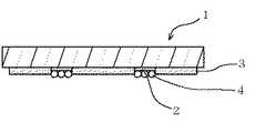
図1は、本発明のバンプレス半導体装置をICチップに適用した例である。このICチップ1の構造は、表面にアルミニウムなどの電極パッド2が設けられ、電極パッド2の周囲には電極パッド2の表面位置レベルよりも高い表面位置レベルのパッシベーション膜3が設けられているバンプレス構造を有する。そして、電極パッド2には、導電性粒子4が金属結合により接続されている。従って、電極パッド2と導電性粒子4との間の接続信頼性は、図3〜図5に示した従来のICチップに形成されたバンプに匹敵するものとなる。しかも、導電性粒子4を電極パッド2に金属結合させる場合、煩雑で高コストの従来のバンプ形成法ではなく、超音波圧着法等の比較的低コストの手法で金属結合させることができる。更に、導電性粒子4として存在しているので、導電性粒子4と回路基板の接続端子(被接続体)との間の接続信頼性も、従来の異方性導電接続法に匹敵するものとなる。
【0017】
本発明において、導電性粒子4としては、半田粒子、ニッケル粒子などの金属粒子や、ベンゾグアナミンなどの樹脂粒子(コア)の表面にニッケルや金等の金属メッキ層が形成された複合粒子を使用することができる。中でも、接続部分に加わる応力を緩和できる樹脂粒子をコアとする複合粒子を使用することが好ましい。
【0018】
導電性粒子4の粒径は、金属結合された導電性粒子4の少なくとも一部が、パッシべーション膜3の表面よりも外側に突出する大きさとすることが好ましい。即ち、パッシベーション膜3と電極パッド2との間の表面位置レベルの差よりも大きくすることが好ましい。これにより、スクライブラインにおけるショートの発生を抑制でき、しかも被接続体(回路基板)に対する接続信頼性を向上させることができる。この場合、導電性粒子4の粒径を、電極パッド2に金属結合可能な範囲で、電極パッド2の径よりも大きくしてもよいが、導電性粒子4同士の横方向のショートをより効率的に抑制するために、導電性粒子4の粒径を電極パッド2の径よりも小さくすることが好ましい。具体的には、導電性粒子4の粒径は、金属粒子である場合には好ましくは1〜50μm、より好ましくは3〜40μmであり、複合粒子の場合には樹脂粒子の直径が好ましくは1〜50μm、より好ましくは3〜40μmであり且つ金属メッキ層の厚みが好ましくは10nm〜1μm、より好ましくは15nm〜1μmである。
【0019】
また、導電性粒子4の最外層として、好ましくは5nm〜0.5μm厚程度の薄い金メッキ層を形成することが、接触抵抗を低減させる点から好ましい。
【0020】
なお、図1の態様におけるICチップ1、電極パッド2、パッシベーション膜3の具体的構成としては、それぞれ従来公知のものを採用することができる。
【0021】
次に、本発明のバンプレス半導体装置(ICチップ)の製造方法を工程毎に説明する。
【0022】
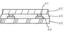
工程(a)
図2(a)に示すように、まず、ガラス平板などの平板21の片面に前述した導電性粒子4を静電気的に吸着させる。この場合、工程(b)における超音波圧着時の導電性粒子の転着を効率的に行うために、単層で吸着させることが好ましい。導電性粒子4を静電気的に平板21に吸着させる手法としては、平板21の表面をポリエステル布等で擦って静電気をチャージし、その面に導電性粒子4を散布すればよい。吸着しなかった導電性粒子については、平板21を傾けあるいは裏返し、平板21に軽く振動を与えることにより除去することができる。
【0023】
工程(b)
次に、図2(b)に示すように、表面に電極パッド2が設けられ、電極パッド2の周囲にはパッシベーション膜3が設けられているICチップ1の電極パッド面2に、平板21の導電性粒子吸着面を重ねて超音波圧着する(図2(c))。これにより、導電性粒子4を電極パッド2に金属結合させて該平板21から電極パッド2に転着させることができる。なお、絶縁膜であるパッシべーション膜3に対しては、導電性粒子4は金属結合しないので転着しない。
【0024】
超音波圧着条件としては、例えば10〜100KHzの周波数を1〜100MPa(電極パッド当たり)の圧力で、0.1〜20秒、印可する条件が挙げられる。使用できる具体的な装置としては、Ultrasonic Micro Welding System(SH40MP、ULTAX社製)が挙げられる。
【0025】
工程(c)
必要に応じて、パッシべーション膜3に付着した導電性粒子4を、市販の粘着テープに転着させるか、あるいはエアブロー処理により吹き飛ばすことにより除去すると、図2(d)に示すバンプレス半導体装置(ICチップ)1が得られる。
【0026】
図2(d)に示したバンプレス半導体装置(ICチップ)1は高い接続信頼性を有する接続構造体を与えることができる。具体的には、接続パッド2に金属結合した導電性粒子4が回路基板5の接続端子6に当接するように、バンプレス半導体装置1と回路基板5とを公知のフィルム状又はペースト状の絶縁性接着材料7で接合された接続構造体(図2(e))を挙げることができる。
【0027】
【実施例】
以下、本発明を実施例により具体的に説明する。
【0028】
実施例1〜8及び比較例1〜4
ガラス平板の片面をポリエステル布で擦った後、その面に表1の導電性粒子を散布して吸着させ、余分の導電性粒子は、ガラス平板を傾けて軽く振動させることにより除去した。但し、実施例6は、導電性粒子としてNiコアの表面にAuメッキ層が設けられた金属粒子を使用したが、その他の実施例及び比較例では、ベンゾグアナミン(コア樹脂粒子)の表面にNiメッキ層及びAuメッキ層が形成された複合粒子を使用した。
【0029】
このガラス平板の導電性粒子吸着面を、片面にアルミ電極パッドが80μmピッチで500個設けられた10mm角のICチップの電極パッド形成面に重ね、ガラス平板側から超音波圧着装置(Ultrasonic Micro Welding System(SH40MP、ULTAX社製))により超音波圧着処理(周波数10、50又は100kHz;圧力49MPa;処理時間10秒)した。これにより、導電性粒子をICチップの電極パッドに金属結合により転着した。パッシべーション膜に付着した余分の導電性粒子をエアブロー処理により吹き飛ばし、図1に示すバンプレス半導体装置(ICチップ)を得た。
【0030】
【表1】
次に、得られたバンプレス半導体装置の電極パッドを、25μm厚のポリイミド回路基板の接続端子(8μm高さの銅に金メッキを施した回路パターン(80μmピッチ))に対して位置合わせし、それらの間に熱硬化型エポキシ系絶縁性接着フィルム(異方性導電接着フィルム(FP16613、ソニーケミカル社製)から導電性粒子を除去したもの)を挟み込み、190℃、圧力1960kPa、10秒という条件で熱圧着し、接続構造体を得た。
【0032】
得られた続構造体について、−55℃←→125℃の間のサーマルショック(1000サイクル)試験を行ったところ、実施例1〜5、7〜8のバンプレス半導体装置を使用した接続構造体は、抵抗上昇がいずれも10mΩ以内であり、優れた接続信頼性を示した。また、実施例6のバンプレス半導体装置を使用した接続構造体は、抵抗上昇が200mΩ程度であったが、実用上問題のないレベルであった。
【0033】
一方、比較例1のバンプレス半導体装置を使用した接続構造体は、コア樹脂粒子径が小さすぎるために、抵抗上昇が1Ωを超えてしまった。比較例2のバンプレス半導体装置を使用した接続構造体は、コア樹脂粒子径が大きすぎるために、パッドに載らない粒子が出現し、初期抵抗値が高くなり使用に適さないものであった。比較例3のバンプレス半導体装置を使用した接続構造体は、コア樹脂粒子表面の金属メッキ層の厚みが薄すぎるために、導電性粒子が転着していない電極パッドが出現し、初期抵抗値が高くなり使用に適さないものであった。また、比較例4のバンプレス半導体装置を使用した接続構造体は、コア粒子表面の金属メッキ層の厚みが厚すぎるために、導電性粒子同士が凝集し、ショートが発生した。
【0034】
【発明の効果】
本発明によれば、ICチップなどの半導体装置を回路基板にフリップチップ方式で接続する際に、半導体装置にバンプを形成することなく、ショートの抑制、接続コストの低減、接続部へのストレス集中の抑制、及びICチップや回路基板に付加されるダメージの低減を図りつつ、高信頼性且つ低コストでICチップと回路基板とを接続することができる。
【図面の簡単な説明】
【図1】本発明のバンプレス半導体装置の概略断面図である。
【図2】本発明のバンプレス半導体装置及び接続構造体の製造工程図である。
【図3】ICチップと回路基板との従来の接続形態の説明図である。
【図4】ICチップと回路基板との従来の接続形態の説明図である。
【図5】ICチップと回路基板との従来の接続形態の説明図である。
【符号の説明】
1 バンプレス半導体装置(ICチップ)、2 電極パッド、3 パッシベーション膜、4 導電性粒子、5 回路基板、6 接続端子[0001]
BACKGROUND OF THE INVENTION
The present invention relates toamethod forproducing abus Npuresu IC chip.
[0002]
[Prior art]
When the bare IC chip is connected to the circuit board by the flip chip method, it is necessary to separate the IC chip from the circuit board in order to prevent occurrence of a short circuit in the scribe line not covered with the passivation film. For this reason, a bump for connection having a height of about 10 μm to 80 μm is widely formed on the IC chip (FIGS. 3 to 5).
[0003]
In the case of the embodiment of FIG. 3, the conductive particles 35 are placed in the binder 36 between the
[0004]
3 and 4, the adhesion force between the IC chip and the circuit board is such that the bump 31 (41) and the connection terminal 34 (44) are not metal-bonded to each other. It depends on the cohesive strength of the binder (adhesive component) in the adhesive (in the insulating adhesive).
[0005]
5, the
[0006]
[Problems to be Solved by the Invention]
However, in the cases of FIGS. 3 to 5, it is assumed that bumps having high processing costs are formed on the IC chip, so that the degree of freedom of the shape of the IC chip is reduced, and the IC chip There is a problem that it is difficult to reduce the connection cost with the circuit board.
[0007]
3 and 4, the bump 31 (41) and the connection terminal 34 (44) are not metal-bonded, so that the adhesion between the IC chip and the circuit board is anisotropically conductive. In the case of the embodiment of FIG. 3 using an anisotropic conductive adhesive, connection reliability can be ensured, depending on the cohesive strength of the binder (adhesive component) in the adhesive (in the insulating adhesive). In the case of the embodiment of FIG. 4 that is not used, there is a problem that the connection reliability is lower than that in the case of metal bonding.
[0008]
Further, in the case of the embodiment of FIG. 3, anisotropic conductive bonding is performed in order to ensure that the conductive particles 35 exist between the
[0009]
On the other hand, in the case of the embodiment of FIG. 5, the
[0010]
The present invention is intended to solve the above-described problems of the conventional technology, and when a semiconductor device such as a bare IC chip is connected to a circuit board by a flip chip method, without forming bumps on the semiconductor device, Connect IC chip and circuit board with high reliability and low cost while suppressing short circuit, reducing connection cost, reducing stress concentration on connection part, and reducing damage to IC chip and circuit board. The purpose is to make it possible.
[0011]
[Means for Solving the Problems]
The inventor once electrostatically adsorbs the conductive particles on a flat plate such as a glass plate, and superposes the conductive particle adsorption surface of the flat plate on the electrode pad side surface of the semiconductor device, thereby ultrasonically pressing the electrode. It has been found that the conductive particles can be metal-bonded only to the pad, and the present invention has been completed.
[0013]
That is , the present invention includes the following steps (a) and (b):
(A) a step of electrostatically adsorbing conductive particles on one surface of a flat plate; and (b) an electrode pad of a bumpless IC chip in which an electrode pad is provided on the surface and a passivation film is provided around the electrode pad. And a conductive particle adsorbing surface of the flat plate is superposed on the surface, and ultrasonic bonding is performed, whereby the conductive particles are metal-bonded to the electrode pad and transferred from the flat plate to the electrode pad. A method of manufacturing a press IC chip is provided.
[0015]
DETAILED DESCRIPTION OF THE INVENTION
Hereinafter, the present invention will be described in detail with reference to the drawings.
[0016]
FIG. 1 shows an example in which the bumpless semiconductor device of the present invention is applied to an IC chip. This IC chip 1 has a structure in which an electrode pad 2 such as aluminum is provided on the surface, and a
[0017]
In the present invention, as the
[0018]
The particle diameter of the
[0019]
Further, it is preferable to form a thin gold plating layer having a thickness of about 5 nm to 0.5 μm as the outermost layer of the
[0020]
In addition, as a specific configuration of the IC chip 1, the electrode pad 2, and the
[0021]
Next, a method for manufacturing a bumpless semiconductor device (IC chip) according to the present invention will be described step by step.
[0022]
Step (a)
As shown in FIG. 2A, first, the
[0023]
Step (b)
Next, as shown in FIG. 2B, the electrode pad 2 is provided on the surface and the
[0024]
Examples of the ultrasonic pressure bonding condition include a condition in which a frequency of 10 to 100 KHz is applied at a pressure of 1 to 100 MPa (per electrode pad) for 0.1 to 20 seconds. Specific devices that can be used include Ultrasonic Micro Welding System (SH40MP, manufactured by ULTAX).
[0025]
Step (c)
If necessary, the
[0026]
The bumpless semiconductor device (IC chip) 1 shown in FIG. 2D can provide a connection structure having high connection reliability. Specifically, the bumpless semiconductor device 1 and the circuit board 5 are insulated in a known film or paste form so that the
[0027]
【Example】
Hereinafter, the present invention will be specifically described by way of examples.
[0028]
Examples 1-8 and Comparative Examples 1-4
After rubbing one side of the glass flat plate with a polyester cloth, the conductive particles shown in Table 1 were sprayed and adsorbed on the surface, and excess conductive particles were removed by tilting the glass flat plate and gently vibrating. However, in Example 6, metal particles having an Au plating layer provided on the surface of a Ni core were used as conductive particles, but in other examples and comparative examples, the surface of benzoguanamine (core resin particles) was Ni plated. Composite particles on which a layer and an Au plating layer were formed were used.
[0029]
The conductive particle adsorption surface of the glass flat plate is overlapped with the electrode pad forming surface of a 10 mm square IC chip having 500 aluminum electrode pads with a pitch of 80 μm on one side, and an ultrasonic pressure bonding device (Ultrasonic Micro Welding) from the glass flat plate side. Ultrasonic pressure bonding (frequency 10, 50 or 100 kHz; pressure 49 MPa; treatment time 10 seconds) was performed using System (SH40MP, manufactured by ULTAX). As a result, the conductive particles were transferred to the electrode pads of the IC chip by metal bonding. Excess conductive particles adhering to the passivation film were blown off by an air blowing process to obtain a bumpless semiconductor device (IC chip) shown in FIG.
[0030]
[Table 1]
Next, the electrode pads of the obtained bumpless semiconductor device are aligned with the connection terminals of a polyimide circuit board having a thickness of 25 μm (a circuit pattern (80 μm pitch) obtained by gold plating on copper having a height of 8 μm). A thermosetting epoxy insulating adhesive film (an anisotropic conductive adhesive film (FP16613, manufactured by Sony Chemicals Co., Ltd.) is sandwiched between them, and the conditions are 190 ° C., pressure 1960 kPa, 10 seconds. A connection structure was obtained by thermocompression bonding.
[0032]
About the obtained continuation structure, when the thermal shock (1000 cycles) test between -55 degreeC ←-> 125 degreeC was done, the connection structure using the bumpless semiconductor device of Examples 1-5 and 7-8 The resistance increase was within 10 mΩ in all cases, indicating excellent connection reliability. Further, the connection structure using the bumpless semiconductor device of Example 6 had a resistance increase of about 200 mΩ, but it was at a level causing no practical problem.
[0033]
On the other hand, in the connection structure using the bumpless semiconductor device of Comparative Example 1, the increase in resistance exceeded 1Ω because the core resin particle diameter was too small. In the connection structure using the bumpless semiconductor device of Comparative Example 2, since the core resin particle diameter was too large, particles that could not be placed on the pad appeared and the initial resistance value was high, which was not suitable for use. In the connection structure using the bumpless semiconductor device of Comparative Example 3, since the thickness of the metal plating layer on the surface of the core resin particles is too thin, an electrode pad to which conductive particles are not transferred appears, and the initial resistance value Was high and unsuitable for use. Further, in the connection structure using the bumpless semiconductor device of Comparative Example 4, the thickness of the metal plating layer on the surface of the core particles was too thick, and the conductive particles aggregated to cause a short circuit.
[0034]
【The invention's effect】
According to the present invention, when a semiconductor device such as an IC chip is connected to a circuit board by a flip chip method, it is possible to suppress short circuit, reduce connection cost, and concentrate stress on the connection portion without forming bumps on the semiconductor device. It is possible to connect the IC chip and the circuit board with high reliability and low cost while suppressing the damage and reducing the damage applied to the IC chip and the circuit board.
[Brief description of the drawings]
FIG. 1 is a schematic cross-sectional view of a bumpless semiconductor device of the present invention.
FIG. 2 is a manufacturing process diagram of a bumpless semiconductor device and a connection structure according to the present invention.
FIG. 3 is an explanatory diagram of a conventional connection form between an IC chip and a circuit board.
FIG. 4 is an explanatory diagram of a conventional connection form between an IC chip and a circuit board.
FIG. 5 is an explanatory diagram of a conventional connection form between an IC chip and a circuit board.
[Explanation of symbols]
1 bumpless semiconductor device (IC chip), 2 electrode pads, 3 passivation film, 4 conductive particles, 5 circuit board, 6 connection terminals
Claims (4)
Translated fromJapanese(a)平板の片面に導電性粒子を静電気的に吸着させる工程;及び
(b)表面に電極パッドが設けられ、電極パッドの周囲にはパッシベーション膜が設けられているバンプレスICチップの電極パッド面に、該平板の導電性粒子吸着面を重ねて超音波圧着することにより、導電性粒子を電極パッドに金属結合させて該平板から電極パッドに転着させる工程
を有することを特徴とするバンプレスICチップの製造方法。The following steps (a) and (b):
(A) a step of electrostatically adsorbing conductive particles on one surface of a flat plate; and (b) an electrode pad of a bumpless IC chip in which an electrode pad is provided on the surface and a passivation film is provided around the electrode pad. the surface, superimposed conductive particles attracting surface of the plate by ultrasonic pressing, characterized in that the conductive particles to the electrode pads by metallic bonds having a step of transferred onto the electrode pad from the flat plateBas Npuresu IC chip manufacturing method of.
Priority Applications (8)
| Application Number | Priority Date | Filing Date | Title |
|---|---|---|---|
| JP2001042378AJP3711873B2 (en) | 2001-02-19 | 2001-02-19 | Bumpless IC chip manufacturing method |
| TW91101960ATW523841B (en) | 2001-02-19 | 2002-02-05 | Bumpless semiconductor device |
| CNB028084640ACN100342513C (en) | 2001-02-19 | 2002-02-18 | Bumpless semiconductor device |
| HK04107876.0AHK1065166B (en) | 2001-02-19 | 2002-02-18 | Bumpless semiconductor device |
| KR1020037010814AKR100973364B1 (en) | 2001-02-19 | 2002-02-18 | Bump Press Semiconductor Device |
| PCT/JP2002/001357WO2002067317A1 (en) | 2001-02-19 | 2002-02-18 | Bumpless semiconductor device |
| US10/467,638US7109058B2 (en) | 2001-02-19 | 2002-02-18 | Bumpless semiconductor device |
| US11/486,075US7638876B2 (en) | 2001-02-19 | 2006-07-14 | Bumpless semiconductor device |
Applications Claiming Priority (1)
| Application Number | Priority Date | Filing Date | Title |
|---|---|---|---|
| JP2001042378AJP3711873B2 (en) | 2001-02-19 | 2001-02-19 | Bumpless IC chip manufacturing method |
Related Child Applications (1)
| Application Number | Title | Priority Date | Filing Date |
|---|---|---|---|
| JP2005149542ADivisionJP2005286349A (en) | 2005-05-23 | 2005-05-23 | Bumpless semiconductor device |
Publications (2)
| Publication Number | Publication Date |
|---|---|
| JP2002246509A JP2002246509A (en) | 2002-08-30 |
| JP3711873B2true JP3711873B2 (en) | 2005-11-02 |
Family
ID=18904679
Family Applications (1)
| Application Number | Title | Priority Date | Filing Date |
|---|---|---|---|
| JP2001042378AExpired - Fee RelatedJP3711873B2 (en) | 2001-02-19 | 2001-02-19 | Bumpless IC chip manufacturing method |
Country Status (6)
| Country | Link |
|---|---|
| US (2) | US7109058B2 (en) |
| JP (1) | JP3711873B2 (en) |
| KR (1) | KR100973364B1 (en) |
| CN (1) | CN100342513C (en) |
| TW (1) | TW523841B (en) |
| WO (1) | WO2002067317A1 (en) |
Cited By (1)
| Publication number | Priority date | Publication date | Assignee | Title |
|---|---|---|---|---|
| KR100665363B1 (en)* | 2005-12-28 | 2007-01-09 | 삼성전기주식회사 | Semiconductor chip package using CMOS process and method for manufacturing same |
Families Citing this family (18)
| Publication number | Priority date | Publication date | Assignee | Title |
|---|---|---|---|---|
| US7045884B2 (en)* | 2002-10-04 | 2006-05-16 | International Rectifier Corporation | Semiconductor device package |
| JP2005108871A (en)* | 2003-09-26 | 2005-04-21 | Sekisui Chem Co Ltd | Metal bump, its forming method, semiconductor chip, and conductive connection structure |
| US20050110126A1 (en)* | 2003-11-25 | 2005-05-26 | Kai-Chiang Wu | Chip adhesive |
| US6993835B2 (en)* | 2003-12-04 | 2006-02-07 | Irvine Sensors Corp. | Method for electrical interconnection of angularly disposed conductive patterns |
| JP3997991B2 (en)* | 2004-01-14 | 2007-10-24 | セイコーエプソン株式会社 | Electronic equipment |
| US7438395B2 (en)* | 2004-09-24 | 2008-10-21 | Brother Kogyo Kabushiki Kaisha | Liquid-jetting apparatus and method for producing the same |
| US7754529B2 (en)* | 2005-02-03 | 2010-07-13 | Panasonic Corporation | Flip chip mounting body and method for mounting such flip chip mounting body and bump forming method |
| KR100801073B1 (en)* | 2005-10-06 | 2008-02-11 | 삼성전자주식회사 | Semiconductor chip provided with bump containing electroconductive particle, and its manufacturing method |
| US7550846B2 (en)* | 2005-12-21 | 2009-06-23 | Palo Alto Research Center | Conductive bump with a plurality of contact elements |
| KR101309319B1 (en)* | 2006-11-22 | 2013-09-13 | 삼성디스플레이 주식회사 | Driving circuit, method of manufacturing thereof and liquid crystal display apparatus having the same |
| TWI397978B (en)* | 2007-12-12 | 2013-06-01 | Ind Tech Res Inst | Structure of chip and process thereof and structure of flip chip package and process thereof |
| US8563357B2 (en)* | 2008-06-26 | 2013-10-22 | Infineon Technologies Ag | Method of packaging a die |
| TWI412107B (en)* | 2009-10-02 | 2013-10-11 | Ind Tech Res Inst | Bump structure, chip package structure including the bump structure, and method of manufacturing the bump sutructure |
| CN102053395B (en)* | 2009-10-28 | 2013-05-01 | 财团法人工业技术研究院 | Bump structure, chip packaging structure and method for preparing the bump structure |
| US20120228768A1 (en)* | 2011-03-07 | 2012-09-13 | Reza Argenty Pagaila | Integrated circuit packaging system using b-stage polymer and method of manufacture thereof |
| JP5614440B2 (en)* | 2011-10-26 | 2014-10-29 | 日立化成株式会社 | Circuit component and manufacturing method thereof |
| KR102847046B1 (en) | 2019-05-08 | 2025-08-18 | 삼성디스플레이 주식회사 | Display device and method of manufacturing for the display device |
| CN119451322B (en)* | 2025-01-09 | 2025-06-13 | 深圳市帝显电子有限公司 | Packaging structure and packaging method of Mini/Micro LED chips |
Family Cites Families (18)
| Publication number | Priority date | Publication date | Assignee | Title |
|---|---|---|---|---|
| JPS54152470A (en) | 1978-05-22 | 1979-11-30 | Nec Corp | Semiconductor device |
| US4618739A (en)* | 1985-05-20 | 1986-10-21 | General Electric Company | Plastic chip carrier package |
| JPH0740496B2 (en)* | 1989-03-01 | 1995-05-01 | シャープ株式会社 | Method of placing conductive particles on electrode |
| JPH0327542A (en) | 1989-06-23 | 1991-02-05 | Seiko Epson Corp | Structure for packaging semiconductor device |
| EP0413335B1 (en) | 1989-08-17 | 1996-05-15 | Canon Kabushiki Kaisha | Method of mutually connecting electrode terminals |
| JPH03185894A (en) | 1989-12-15 | 1991-08-13 | Canon Inc | Mutual connection of electrode terminal |
| JP2704033B2 (en) | 1990-07-23 | 1998-01-26 | キヤノン株式会社 | How to connect electrode terminals |
| JPH0547839A (en) | 1991-08-09 | 1993-02-26 | Seiko Epson Corp | Semiconductor integrated circuit device mounting method |
| JPH05110243A (en) | 1991-10-17 | 1993-04-30 | Fujitsu Ltd | Wire joining method |
| JPH0682749A (en)* | 1992-09-01 | 1994-03-25 | Seiko Epson Corp | Chip mounting method, chip mounting structure, and electro-optical device and electronic printing device using it |
| US5420520A (en)* | 1993-06-11 | 1995-05-30 | International Business Machines Corporation | Method and apparatus for testing of integrated circuit chips |
| JPH0737890A (en) | 1993-07-16 | 1995-02-07 | Matsushita Electric Ind Co Ltd | Solder ball joining apparatus and joining method thereof |
| JPH07297228A (en)* | 1994-04-22 | 1995-11-10 | Victor Co Of Japan Ltd | Method for connecting boards with each other |
| WO1996042107A1 (en)* | 1995-06-13 | 1996-12-27 | Hitachi Chemical Company, Ltd. | Semiconductor device, wiring board for mounting semiconductor and method of production of semiconductor device |
| US5917242A (en)* | 1996-05-20 | 1999-06-29 | Micron Technology, Inc. | Combination of semiconductor interconnect |
| US5677567A (en)* | 1996-06-17 | 1997-10-14 | Micron Technology, Inc. | Leads between chips assembly |
| KR100467897B1 (en) | 1996-12-24 | 2005-01-24 | 닛토덴코 가부시키가이샤 | A semiconductor device and a process for the production thereof |
| JP3660175B2 (en)* | 1998-11-25 | 2005-06-15 | セイコーエプソン株式会社 | Mounting structure and method of manufacturing liquid crystal device |
- 2001
- 2001-02-19JPJP2001042378Apatent/JP3711873B2/ennot_activeExpired - Fee Related
- 2002
- 2002-02-05TWTW91101960Apatent/TW523841B/ennot_activeIP Right Cessation
- 2002-02-18CNCNB028084640Apatent/CN100342513C/ennot_activeExpired - Fee Related
- 2002-02-18KRKR1020037010814Apatent/KR100973364B1/ennot_activeExpired - Fee Related
- 2002-02-18USUS10/467,638patent/US7109058B2/ennot_activeExpired - Fee Related
- 2002-02-18WOPCT/JP2002/001357patent/WO2002067317A1/enactiveApplication Filing
- 2006
- 2006-07-14USUS11/486,075patent/US7638876B2/ennot_activeExpired - Fee Related
Cited By (1)
| Publication number | Priority date | Publication date | Assignee | Title |
|---|---|---|---|---|
| KR100665363B1 (en)* | 2005-12-28 | 2007-01-09 | 삼성전기주식회사 | Semiconductor chip package using CMOS process and method for manufacturing same |
Also Published As
| Publication number | Publication date |
|---|---|
| JP2002246509A (en) | 2002-08-30 |
| WO2002067317A1 (en) | 2002-08-29 |
| US20040217460A1 (en) | 2004-11-04 |
| US7109058B2 (en) | 2006-09-19 |
| CN100342513C (en) | 2007-10-10 |
| US7638876B2 (en) | 2009-12-29 |
| KR20030081451A (en) | 2003-10-17 |
| KR100973364B1 (en) | 2010-07-30 |
| TW523841B (en) | 2003-03-11 |
| US20060249856A1 (en) | 2006-11-09 |
| CN1503988A (en) | 2004-06-09 |
| HK1065166A1 (en) | 2005-02-08 |
Similar Documents
| Publication | Publication Date | Title |
|---|---|---|
| JP3711873B2 (en) | Bumpless IC chip manufacturing method | |
| JP3921459B2 (en) | Mounting method and mounting apparatus for electrical parts | |
| JP3663938B2 (en) | Flip chip mounting method | |
| JP3420917B2 (en) | Semiconductor device | |
| JP3927759B2 (en) | Mounting electronic components on a circuit board | |
| CN101252093A (en) | Manufacturing method of electronic component and electronic device | |
| JP3727587B2 (en) | Mounting method of semiconductor device | |
| JP3687280B2 (en) | Chip mounting method | |
| JP2001332583A (en) | Semiconductor chip mounting method | |
| JPH09246319A (en) | Flip chip mounting method | |
| JP2005286349A (en) | Bumpless semiconductor device | |
| JP2007103953A (en) | Semiconductor chip having bumps containing conductive particles and method for manufacturing the same | |
| KR101753066B1 (en) | A film comprising conductive particle and the manufacturing method of flip chip package using the same | |
| JP4118974B2 (en) | IC chip mounting substrate and method of manufacturing IC chip mounting substrate | |
| JPH11135561A (en) | Anisotropic conductive adhesive film, its manufacture, flip-chip mounting method, and flip-chip packaging board | |
| JP3553246B2 (en) | Method of manufacturing IC module for IC card and method of manufacturing IC module | |
| HK1065166B (en) | Bumpless semiconductor device | |
| JPH06151507A (en) | Terminal electrode on circuit board, forming method thereof and mounted body | |
| KR20010069358A (en) | Semiconductor chip bonding by eutectic alloy balls embedded in anisotropic conducting film | |
| JP3702929B2 (en) | Wire bonding method | |
| JPH10256306A (en) | Preparation of circuit board | |
| JP3949402B2 (en) | Semiconductor device and manufacturing method thereof | |
| JP3383774B2 (en) | Semiconductor element mounting method | |
| JP3882967B2 (en) | Circuit board manufacturing method | |
| JP2005093600A (en) | Method for manufacturing circuit board having protruding electrode and method for connecting circuit board and semiconductor element |
Legal Events
| Date | Code | Title | Description |
|---|---|---|---|
| A131 | Notification of reasons for refusal | Free format text:JAPANESE INTERMEDIATE CODE: A131 Effective date:20040803 | |
| A521 | Written amendment | Free format text:JAPANESE INTERMEDIATE CODE: A523 Effective date:20041004 | |
| A131 | Notification of reasons for refusal | Free format text:JAPANESE INTERMEDIATE CODE: A131 Effective date:20041102 | |
| RD02 | Notification of acceptance of power of attorney | Free format text:JAPANESE INTERMEDIATE CODE: A7422 Effective date:20041228 | |
| A02 | Decision of refusal | Free format text:JAPANESE INTERMEDIATE CODE: A02 Effective date:20050322 | |
| A521 | Written amendment | Free format text:JAPANESE INTERMEDIATE CODE: A523 Effective date:20050523 | |
| A911 | Transfer to examiner for re-examination before appeal (zenchi) | Free format text:JAPANESE INTERMEDIATE CODE: A911 Effective date:20050704 | |
| TRDD | Decision of grant or rejection written | ||
| A01 | Written decision to grant a patent or to grant a registration (utility model) | Free format text:JAPANESE INTERMEDIATE CODE: A01 Effective date:20050726 | |
| A61 | First payment of annual fees (during grant procedure) | Free format text:JAPANESE INTERMEDIATE CODE: A61 Effective date:20050808 | |
| R150 | Certificate of patent or registration of utility model | Free format text:JAPANESE INTERMEDIATE CODE: R150 | |
| FPAY | Renewal fee payment (event date is renewal date of database) | Free format text:PAYMENT UNTIL: 20080826 Year of fee payment:3 | |
| FPAY | Renewal fee payment (event date is renewal date of database) | Free format text:PAYMENT UNTIL: 20090826 Year of fee payment:4 | |
| FPAY | Renewal fee payment (event date is renewal date of database) | Free format text:PAYMENT UNTIL: 20090826 Year of fee payment:4 | |
| FPAY | Renewal fee payment (event date is renewal date of database) | Free format text:PAYMENT UNTIL: 20100826 Year of fee payment:5 | |
| FPAY | Renewal fee payment (event date is renewal date of database) | Free format text:PAYMENT UNTIL: 20110826 Year of fee payment:6 | |
| FPAY | Renewal fee payment (event date is renewal date of database) | Free format text:PAYMENT UNTIL: 20110826 Year of fee payment:6 | |
| FPAY | Renewal fee payment (event date is renewal date of database) | Free format text:PAYMENT UNTIL: 20120826 Year of fee payment:7 | |
| FPAY | Renewal fee payment (event date is renewal date of database) | Free format text:PAYMENT UNTIL: 20120826 Year of fee payment:7 | |
| FPAY | Renewal fee payment (event date is renewal date of database) | Free format text:PAYMENT UNTIL: 20130826 Year of fee payment:8 | |
| R250 | Receipt of annual fees | Free format text:JAPANESE INTERMEDIATE CODE: R250 | |
| R250 | Receipt of annual fees | Free format text:JAPANESE INTERMEDIATE CODE: R250 | |
| R250 | Receipt of annual fees | Free format text:JAPANESE INTERMEDIATE CODE: R250 | |
| R250 | Receipt of annual fees | Free format text:JAPANESE INTERMEDIATE CODE: R250 | |
| LAPS | Cancellation because of no payment of annual fees |